Fully printed phased-array antenna for space communications Maggie Yihong Chen*a, Xuejun Lub, Harish Subbaramanc, Ray T. Chenc Omega optics Inc., 10435 Burnet Rd STE 108, Austin, TX, USA 78758; b University of Massachusetts Lowell, One University Avenue, Lowell, MA, USA 01854; c The University of Texas at Austin, 10100 Burnet Rd., Austin, TX, USA 78758 ABSTRACT We present a flexible active 2-bit 2-element phased-array antenna (PAA) fully fabricated using ink-jet printing technology. High speed carbon nanotube (CNT) based field effect transistors (FETs) function as switch in the true-time delay line of the PAA. The 2-bit 2-element active PAA is printed out at room temperature on 100μm thick Kapton substrate. The FET switch works well for 5GHz RF signals. An ON-OFF ratio of over 100 is obtained at a low Vds bias of 1.8V. The measured azimuth beamsteering angles of PAA agree well with simulation values. Keywords: Phased-array antenna, true-time delay, carbon-nanotube, field effect transistor, space communication
1. INTRODUCTION NASA’s future exploration missions focus on the manned exploration of the Moon, Mars and beyond, which will rely heavily on the development of a reliable communications infrastructure from planetary surface-to-surface, surface-toorbit and back to Earth. Different communication tasks require different antenna technologies. For example, proximity surface activity applications such as robotic rovers, human extravehicular activities (EVA), and probes will require small size, lightweight, and low power antennas in accommodating the desired frequencies and data services in a restricted space. While low profile, conformal antenna designs would be ideal for simple integration into/onto the EVA suit. While lightweight, conformal phased array antennas are significant in NASA’s space and interplanetary exploring missions, such technology is still in immature stage of development. The major deterrent to such systems is the lack of integrated electronics circuits on the flexible surface [1, 2]. To date, the major way to achieve flexible integrated circuits is to attach and interconnect electronics chips onto the antenna surface. The most recent research in conformal phased array antennas is the active membrane phased array radar developing by NASA Jet Propulsion Laboratory (JPL) research group [3]. However, the T/R module is assembled independently and attached to the membrane array, which greatly jeopardize the reliability. Current state-of-the-art flexible electronics are based on organic or polymer materials, such as regioregular poly (3hexylthiophene) derivatives and pentacene. While the organic material based flexible electronic circuits can be monolithically integrated with flexible antennas, the carrier (electron or hole) mobility of these materials is less than 0.1cm2/V·s. Amorphous silicon shows a higher carrier mobility of ~1cm2/Vs [4]. However, it is still two orders of magnitude lower than conventional single crystal silicon. Such low carrier mobility limits the operating frequency of the organic or polymer based flexible electronics circuit to a few kHz [4]. The low operating frequency makes this kind of electronics unsuitable for active PAA applications, where multi-GHz operating frequency is required for different communication bands [5-9]. Carbon nanotubes (CNTs), a material with exceptional aspect ratio and great mechanical flexibility, have been proposed for use to make high-speed FETs [10-18]. Extraordinary field-effect mobility as high as 79,000 cm2/Vs was reported in the FETs based on individual CNTs [11]. Due to the ultra-high field-effect mobility, CNT based flexible FET are capable of achieving high-speed (GHz) operation [19-21]. In the presented research work, ultra-pure electronic-grade CNT solutions are used in the ink-jet printing technology without using any photolithography fabrication steps. An ultra-high operating frequency of over 5 GHz is demonstrated with an ON-OFF ratio of over 100. 2-bit 2-element phased-array antenna is printed incorporating the FET switch based true-time delay lines. Both the theoretical values and measurement results are compared for -30˚ beamsteering of the PAA. *
[email protected]; phone 1 512 996-8833; fax 1 512 873-7744
Micro- and Nanotechnology Sensors, Systems, and Applications, edited by Thomas George, M. Saif Islam, Achyut K. Dutta, Proc. of SPIE Vol. 7318, 731814 · © 2009 SPIE · CCC code: 0277-786X/09/$18 · doi: 10.1117/12.819036
Proc. of SPIE Vol. 7318 731814-1
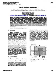
2. DESIGN OF FET AND 2-BIT 2-ELEMENT PAA 2.1 Design of high speed FET The schematic structure of the CNT based FET is shown in Fig. 1. The FET is in a top gated configuration. It consists of source (S) and drain (D) electrodes, a carrier transport layer based on an ultrapure, high density (> 1000 CNTs per μm2) carbon nanotube thin film, an ion-gel gate dielectric layer, and top gate electrode (G). The channel width and length are 200µm and 100 µm, respectively.
I
Gate ate dielectric
PrintaHe nanomaterials Plastic subatrse
I.
100pm
Fig. 1. The schematic structure of the CNT based FET.
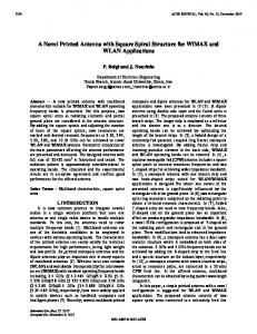
2.2 Design of 2-bit 2-element PAA Fig. 2 shows the layout of the 2-bit 2-element phased array antenna subsystem. First, the RF signal is applied through microwave probe on the coplanar waveguide. Then the signal is transited onto microstrip line. The signal then is split into two branches, with each branch split again by a 1x2 splitter. Then there are four paths with different lengths of delay lines controlled by the FET switch. The time delay between adjacent elements of a PAA can be calculated as
t=
d sin(θ ) c
(1)
Where d is the distance between adjacent element; c is the light velocity; and θ is the beam steering angle. In our design, d is equal to half wavelength to avoid grating effect. The length difference between delay lines can be calculated as
Ldiff =
tc n
(2)
Where n is the refractive index of the microwave propagation media. And here we assume it to be 1.5. Four possible azimuth steering angles are designed according to the above equations, which are -30˚, 0˚, 14.5˚, and 48.6˚. The working frequency is targeted at 5GHz (C-band). The corresponding delay lengths and the steering angles are listed in Table 1. Delay
FET
1
2 Two patch
3 Coplanar waveguide
4 Coplanar waveguide
Fig. 2. Layout of the 2-bit 2-element phased array antenna subsystem.
Proc. of SPIE Vol. 7318 731814-2
Table 1. Corresponding delay lengths and the steering angles of PAA. Line pair
delay
Steering angle
2, 4
0
0
2, 3
-1cm
-30˚
1, 3
0.5cm
14.5 ˚
1, 4
1.5cm
48.6 ˚
3. EXPERIMENTAL RESULTS The whole 2-bit 2-element PAA is printed using the Optomec's M3D Aerosol Jet® printing system [22] on a DuPont™ Kapton® FPC polyimide film [23], which is used in a wide variety of applications such as substrates for flexible printed circuits, transformer and capacitor insulation and bar code labels. During the printing of FET structures, the source and drain electrodes are first printed on the Kapton® FPC polyimide film using the silver nanoparticle ink, followed by the thermal annealing. The width of the source and drain electrodes are 50 µm, and the separation between the source and drain electrodes, i.e., channel length (l), is 100 µm. An active carrier transport layer is then printed using an ultrapure, electronic grade carbon nanotube solution (CJ-28) from Brewer Science Inc. A thin-layer of ion-gel is then printed on top of the CNT film as the gate dielectric [24]. The FET is finished by printing a conducting polymer poly (3, 4ethylenedioxythiophene) (PEDOT) layer as the top gate electrode [25]. 3.1 Characterization of high speed FET Fig. 3 shows the source-drain I-V characteristics (IDS vs. VDS) of the CNT-FET at different gate voltages (VG). The gate voltages vary from -1.0V to +1.5V. At the same source-drain voltage (VDS), lower source-drain currents (IDS) are observed as the gate voltage increases from negative to positive voltages. This indicates that the CNT network in this FET is a p-type carrier (hole) transport layer [26-27]. At the source-drain voltage (VDS) of 1.8V, a high source-drain current (IDS) of 221µA, and a low IDS of 1.6 µA are obtained at the gate voltage of -1.0V and +1.5V, respectively. The source-drain current (IDS) ON-OFF ratio is over 100. The large ON-OFF ratio reveals a high content of the semiconducting type of CNTs in the CNT active layer. The gate-source leakage current (IGS) is measured to be in the pA range. 250
VG =-1.OV
200 -
150-
/0.5
100 -
50
0.2
0.4
0.6
0.8
1
1.2
1.4
t6
1.8
2
V0 (V)
Fig. 3. Source-drain I-V characteristics (IDS vs. VDS) of the fabricated CNT-FET at different gate voltages (VG).
We also test the performance of the FET in an external circuit - a voltage buffer stage, which provides high input impedance and low output impedance. The gate and drain electrodes function, respectively, as the input and output terminals. As indicated in Fig. 4, a clean spectrum and excellent linearity is obtained. The left peak and the center peak of the spectrum are the DC and AC components of the output signal, respectively. These test results shows the FET is compatible with external circuits.
Proc. of SPIE Vol. 7318 731814-3
- -- - - -uuiuuuui I 'lull".', uuuiiii .iu.u.um
I'll'.".
uuauuu rriuu FtIIIU
ftJUUU 0
Fig. 4 Spectrum of the output signal; left peak: DC component of the output signal; right peak: AC component of the spectrum.
3.2 Characterization of 2-bit 2-element PAA Fig. 5 shows the entire measurement setup with the network analyzer, receiving horn and microwave signal analyzer. The 8510C HP network analyzer provides RF signal up to 50GHz. The radiation from the antenna array is received by a standard horn antenna which can be rotated to measure the far field pattern of the antenna array. The received signal from the standard horn antenna is read out using the microwave signal analyzer (MSA). The signal strength at various angles is measured to get the far field patterns. Network analyzer
Microwave signal analyzer
Fig. 5. Beamsteering measurement setup with RF source and microwave signal analyzer.
We measure all the four azimuth steering angles, and shown here is -30˚ beamsteering. The theoretical values and measurement results are compared, which are shown in Fig. 6. The measurement results agree well with simulation values.
1
-30 degree steering
0
Normalized Power (dB)
-50
-40
-30
-20
-10
0
10
20
-1 -2
Simulation Measurement
-3 -4 -5 -6 -7 -8 -9
Angle (Degrees)
Fig. 6. The theoretical values and measurement results of far field patterns for -30˚ steering.
Proc. of SPIE Vol. 7318 731814-4
4. CONCLUSION In summary, we demonstrate an all-ink-jet-printed 2-bit 2-element active PAA operating at 5GHz on a DuPont™ Kapton® FPC polyimide film by using an Optomec's M3D Aerosol Jet® printing system. Adopting electronic grade CNT network solution, we fabricate a high-speed (5 GHz) FET with a large high ON-OFF ratio of over 100. The true-time delay lines incorporated the high speed FET switches are proven to work well through the beamsteering experiments of PAA. All the fabrication processes are performed at room temperature. Such a low temperature processing method allows us to use virtually any flexible substrate such as a regular transparency as demonstrated in our fabrication. The fully printed active PAA technology will greatly benefit the development of space communication antennas. This research was supported by NASA under contract # NNX08CB39P. We acknowledge helpful discussions with Dr. Félix A. Miranda and Mr. James Nessel at Glenn Research Center.
REFERENCES [1] [2] [3]
[4] [5] [6] [7]
[8] [9] [10] [11] [12] [13] [14] [15]
[16]
[17]
James J. Komiak et al, “Design and Performance of Octave S/C-Band MMIC T/R Modules for Multi-Function Phased Arrays,” IEEE Trans. Microwave Theory Tech., Vol. 39, pp. 1955 (1991). Toshiharu Sasaki et al, “Ultra Small Size X band MMIC T/R Module for Active Phased Array,” IEEE MTT-S Digest, pp. 1531 (1992). A. Moussessian, L. Del Castillo, J. Huang, G. Sadowy, J. Hoffman, P. Smith, T. Hatake, C. Derksen, B. Lopez, E. Caro, “An Active Membrane Phased Array Radar,” The IEEE MTT-S International Microwave Symposium, Long Beach, CA, June (2005). H. Meiling and R. E. I. Schropp, “Stable amorphous-silicon thin-film transistors,” Applied Physics Letters, vol. 70, pp. 2681 (1997). S. Jeon, Young-Wan Kim, Deog-Gil Oh, “A new active phased array antenna for mobile direct broadcasting satellite reception,” IEEE Transactions on Broadcasting, Vol. 46, pp. 34 (2000). R. A. Flynt, F. Lu, J. A. Navarro, C. Kai, “Low cost and compact active integrated antenna transceiver for system applications,” IEEE Transactions on Microwave Theory and Techniques, Vol. 44, pp. 1642 (1996). A. Dreher, N. Niklasch, F. Klefenz, A. Schroth, “Antenna and receiver system with digital beamforming for satellite navigation and communications,” IEEE Transactions on Microwave Theory and Techniques, Vol. 51, pp. 1815 (2003). Huang, Lou, Feria, and Kim, “An inflatable L-band microstrip SAR array,” IEEE AP-S/URSI Symposium, Atlanta, GA, pp. 2100-2103, June (1998). J. Huang and A. Moussessian, “Thin-membrane aperturecoupled L-band patch antenna,” IEEE AP-S/URSI Symposium, Monterey, CA, June (2004). S. J. Tans, A. R. M. Verschueren, and C. Dekker, “Room temperature transistor based on a single carbon nanotube,” Nature, 393, pp. 49-52, 1998. T. Durkop, S. A. Getty, E. Cobas, and M. S. Fuhrer, “Extraordinary mobility in semiconducting carbon nanotubes,” Nano Letters, 4, 35-39 (2004). E. Artukovic, M. Kaempgen, D. S. Hecht, S. Roth, and G. Gruner, “Transparent and flexible carbon nanotube transistors,” Nano Letters, 5, 757-760 (2005). E. S. Snow, P. M. Campbell, M. G. Ancona, and J. P. Novak, “High-mobility carbon-nanotube thin-film transistors on a polymeric substrate,” Applied Physics Letters, 86, 033105, (2005). Y. Zhou, A. Gaur, S. Hur, C. Kocabas, M. A. Meitl, M. Shim, and J. A. Rogers, “p-channel, n-channel thin film transistors and p-n diodes based on single wall carbon nanotube networks,” Nano Letters, 4, 2031-2035 (2004). S. Hur, M. Yoon, A. Gaur, M. Shim, A. Facchetti, T. J. Marks, and J. A. Rogers, “Organic nanodielectrics for low voltage carbon nanotube thin film transistors and complementary logic gates,” Journal of the American Chemical Society, 127, 13808-13809 (2005). Q. Cao, M. Xia, M. Shim, and J. A. Rogers, “Bilayer organic-inorganic gate dielectrics for high-performance, lowvoltage, single-walled carbon nanotube thin-film transistors, complementary logic gates, and p-n diodes on plastic substrates,” Advanced Functional Materials, 16, 2355-2362 (2006). Q. Cao, S. Hur, Z. Zhu, Y. Sun, C. Wang, M. A. Meitl, M. Shim, and J. A. Rogers, “Highly-bendable, transparent thin-film transistors that use carbon-nanotube-based conductors and semiconductors with elastomeric dielectrics,” Advanced Materials, 18, 304-309 (2006).
Proc. of SPIE Vol. 7318 731814-5
[18]
[19] [20] [21] [22] [23] [24] [25] [26] [27]
D. R. Hines, S. Mezhenny, M. Breban, E. D. Williams, V. W. Ballarotto, G. Esen, A. Southard, and M. S. Fuhrer, “Nanotransfer printing of organic and carbon nanotube thin-film transistors on plastic substrates,” Applied Physics Letters, 86, 163101, (2005). S. Rosenblatt, H. Lin, V. Sazonova, S. Tiwari, and P. L. McEuen, “Mixing at 50 GHz using a single-walled carbon nanotube transistor,” Applied Physics Letters, 87, 153111, (2005). A. A. Pesetski, J. E. Baumgardner, E. Folk, J. X. Przybysz, John D. Adam, and Hong Zhang. “Carbon nanotube field-effect transistor operation at microwave frequencies,” Applied Physics Letters, 88, 113103, (2006). S. Li, Z. Yu, S. Yen, W. C. Tang, and P. J. Burke, “Carbon Nanotube Transistor Operation, at 2.6 GHz,” Nano Letters, 4, 753, (2004). Optomec product: (http://www.optomec.com/site/m3d_2). Dupont Kapton product data sheet: (http://www2.dupont.com/Kapton/en_US/assets/downloads/pdf/FPC_datasheet.pdf) J. Lee, M. J. Panzre, Y. He, T. Lodge, and C. D. Frisbie, “Ion Gel Gated Polymer Thin-film Transistors,” J. AM. Chem. Soc. 129, 4532-4533 (2007). H. Sirringhaus, T. Kawase, R. H. Friend, T. Shimoda, M. Inbasekaran, W. Wu, E. P. Woo, “High-resolution inkjet printing of all-polymer transistor circuits,” Science, 290, 2123-2126 (2000). J. Vaillancourt, X. Lu, X. Han, and D. C. Janzen, “A high-speed thin-film transistor on flexible substrate fabricated at room temperature,” IEE Electronic Letters, 42, 1365-1367 (2006). X. Han; D. Janzen, J. Vaillancourt, and X. Lu; “Printable High-Speed Thin-Film Transistor on Flexible Substrate Using Carbon Nanotube Solution,” Micro & Nano Letters, 2, pp. 96 (2007).
Proc. of SPIE Vol. 7318 731814-6