such as Verilog, or transform it to HDL description for further ASIC or FPGA ..... and LDD-to-Verilog interface has been tested on Intel Pentium-4 (1.6 GHz) ...
Automation and Remote Control, Vol. 65, No. 6, 2004, pp. 913–919. Translated from Avtomatika i Telemekhanika, No. 6, 2004, pp. 84–92. c 2004 by Wahid, Lu, Rahman. Original Russian Text Copyright �
DECISION DIAGRAMS
HDL Constructs in Linear Word-Level Decision Diagram Based Specification1 K. Wahid, D. C. Lu, and C. Rahman Department of Electrical and Computer Engineering, University of Calgary, Calgary, Canada Received December 16, 2003
Abstract—Linear Decision Diagrams (LDDs) are used in the paper as an intermediate format that allows us to quickly generate the circuit netlist from HDL (hardware description language), such as Verilog, or transform it to HDL description for further ASIC or FPGA synthesis and verification. The results of an extensive experimental study (on memory requirements, run time to convert LDD intermediate format to/from HDL, and verification via simulation) are reported here.
1. INTRODUCTION Hardware description languages, like VHDL and Verilog HDL [2], are used for describing the design at the register-transfer level, and software simulation of the design is the primary tool to do verification. However, input/output signal generation for simulation is impractical for large designs. Consequently, designers have been looking to formal methods, such as Binary Decision Diagrams (BDD). The formal description must allow for migration from one target technology to another, i.e., must be technology independent. The translating of a high-level description of the design into a specific implementation is provided by system synthesis tools. Input of such a tool is typically Verilog, VHDL, etc., and output is a netlist, i.e., a machine-form description of primitive logic elements (gates, cells, memory elements) that can be used by low-level tools to complete the synthesis process with physical implementation. For example, the output can be a netlist for ASIC layout, or a standard cell ASIC desing. An example of system synthesis tools is Synopsys tools that translates VHDL or Verilog to a gate-level netlist. There are systems where the synthesis, simulation and design are all implemented, for example, Cadence suite (synthesize FPGA or ASIC cell design from VHDL or Verilog), Mentor Graphics tools (translate ANSI C or dataflow language to ASIC). After synthesis, the design must be verified. The formal tools for verification can be used at that phase as well, for instance, DD are widely used for that. Problem formulation: We are aiming at that the usage of the structurally simple and compact Linear DDs as an intermediate format that allows us to quickly generate circuit netlist from HDL, such as Verilog, or transform it to HDL description for further ASIC or FPGA synthesis and verification. The interface between low-level and high-level description (LDD) is an important function of an LDD based design automation tool, since it means a direct mapping in the Rapid Prototyping process. 1
This work was supported by Natural Sciences and Engineering Council of Canada (NSERC), project no. 239025-02. c 2004 MAIK “Nauka/Interperiodica” 0005-1179/04/6506-0913 �
914
WAHID et al.
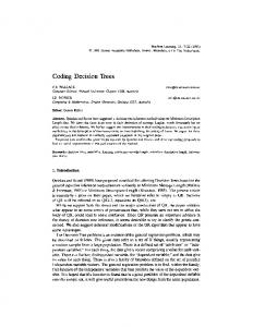
2. DESIGN SPECIFICATION AND SIMULATION VIA WORD-LEVEL DDS Due to their ability to efficiently represent arithmetic operations, Word-level DDs have found their application in verification of high-level circuit description. Verification is possible because these DDs are canonical structures. In [1], Word-level DDs are considered as a tool for bridging the gap between verification of high-level Hardware Description Languages (HDLs) and the netlists consisting of basic gates. For that, the authors presented a complete set of datapath operations that can be formally verified based on Word-level DDs as they found an effective way to translate many HDL commands into a Word-level DD, called K*BMD, in particular, new algorithms for modulo operation and division. However, though they can handle functions with up to several hundred variables, those operations have exponential worst case behavior, while previously known algorithms fail for more than 16 bits. A special type of Word-level DDs, LDDs [4] can handle functions, for which ROBDD or even K*BMD are out of memory or time. This is due to their linear structure and special encoding technique for large word-level coefficients. However, in contrast to WDD, they are semi-canonical (canonical with respects to the level order), and, thus, their usefulness to verification is sacrificed against their linearity. Representation of logic circuits using LDD follows the philosophy: the circuit is levelized, each level is treated as a multi-input multi-output function, an LDD is created for each gate in the level. Note that the LDD describes the multi-output function so that it has Linear arithmetical representation. Then, an LDD that comprises those LDD is generated. The latest LDD describes the level. A set of l LDDs represents the l-level circuit. The original outputs of the levels can be restored, or extracted, using so-called masking operator [5]. Example 2.1. A circuit that includes 4 levels INi , i = 1, 2, 3, 4 (Fig. 1a), can be described by the four Linear arithmetical expressions: IN1 = 20 x2 + 22 x3 + 20 + 22 , IN2 = (20 + 24 )x1 + 22 x2 + 20 x2 + (22 + 24 )x3 , IN3 = 20 y1 + 20 y2 + 20 , IN4 = 20 z1 + 20 z2 . Here, t1 = x2 = Ξ1 {IN1 },
y1 = Ξ2 {IN2 },
z2 = Ξ6 {IN2 },
t2 = x3 = Ξ3 {IN1 },
y2 = Ξ4 {IN2 },
z1 = Ξ2 {IN3 },
f = Ξ1 {IN4 }.
A simulation of circuit behavior using LDD is implemented by the calculations of the Linear arithmetical expressions values, which are the circuit output values, given input values. Example 2.2. For a circuit shown in Fig. 1a, calculate thevalue of the function f given x1 x2 x3 = 101. Since IN1 = 22 + 20 + 22 = 9 = 10012 , then t1 = x2 = Ξ1 {IN1 } = Ξ1 {1001} = 1,
t2 = x3 = Ξ3 {IN1 } = Ξ1 {1001} = 0.
For the second level, IN2 = 20 + 24 + 20 = 18 = 0100102 ,
y1 = Ξ2 {IN2 } = Ξ2 {010010} = 1,
z2 = Ξ6 {IN2 } = Ξ6 {010010} = 0,
y2 = Ξ4 {IN2 } = Ξ5 {010010} = 0.
AUTOMATION AND REMOTE CONTROL
Vol. 65
No. 6
2004
HDL CONSTRUCTS
915
(a)
IN1
(b)
IN4
IN3
IN2
x1 x2
y1
x3 x2
y2
//Example Verilog File
z1
f
x1 z2
x3
module test (f, x1, x2, x3); output f; input x1, x2, x3; wire a, b, y1, y2, z1, z2;
pDA
pDA
pDA
0
x2
0
x1
pDA
0
pDA
0
0
x3
20+21
21
2
0
x2
pDA
0
x2
pDA
0
0
x3
22
2 +2
4
pDA
0
y1
0
z1
pDA
0
pDA
0
0
y2
20
20
2
0
z2
0
20
2
not not nand nand nand or xor
20
(a, x2); (b, x3); (y1, x1, a); (y2, b, x2); (z2, x1, b); (z1, y1, y2); (f, z1, z2);
22+24
Fig. 1. The circuit, (a) LDD model and (b) Verilog file to describe the circuit.
For the third level, IN3 = 20 + 20 = 2 = 102 ,
z1 = Ξ2 {IN3 } = Ξ2 {10} = 1.
Finally, IN4 = 20 = 1 = 012 ,
f = Ξ1 {IN4 } = Ξ1 {01} = 1.
3. INTERFACE FOR HDL-TO-LDD AND LDD-HDL MAPPING The software to handle LDDs works with high-level synthesis description of the circuits. In order to organize an interface with low-level description formats, like VHDL and Verilog HDL, the package must implement direct translation of LDD to HDL constructs. The features of the LDD based representation impose some restrictions on the translation of Verilog HDL constructs to LDDs. Manipulations of LDD are not the subject of this paper, however, we consider the results of such manipulations as a subject to be transformed to VHDL and Verilog description, in case, for example, we need a verification of the design. So, we consider LDD format as an intermediate in a synthesis tool that can quickly generate circuits from Verilog HDL, and also can convert the internal format, LDD, to Verilog or VHDL description for further usage. The latter is the case when the regular layout (of the LDD) can be used at the lower levels, i.e., in logic synthesis. This finds its application in rapid prototyping of embedded systems via Reprogrammable devices. 3.1. Transformation of Verilog Description to LDD The parser input is a structural Verilog file specifying the network of logic gates and the output is an internal object used for further LDD generation for the same circuit. The parser includes two classes. The first one (i) reads the Verilog file and stores all the necessary gate information, then AUTOMATION AND REMOTE CONTROL
Vol. 65
No. 6
2004
916
WAHID et al.
(ii) it creates the gate objects from that gate information, and creates the wiring information of the gate objects. The second class completes the parsing with the information on gates fan-in, and fan-out. The pseudo-code of the algorithm is given below. procedure convertV erilogtoLDD: { for( ∀ line in Verilog file) { create StringVector (InputString table, InputID table and InputGateName table); read through the whole file; if (InputGateName = gateID) create Gate table; end if for ( ∀ line in Gate) { if (GateFanOut = 0) copy GateID into Gate and set Out name; add all FanOut names into Gate; end if set GlobalID = 1; read InputString table and count total number of FanIn and FanOut; call BenchmarkXNFNet and create Gate Object; read Gate table and build GateFanIn and GateFanOut table; } for ( ∀ gate g in network) { if (GateFanIn > 0) & (GateFanOut > 0) copy GateID, set WireName and create WireString table; elseif (GateFanIn = 0) & (GateFanOut = 0) check for any unlisted FanInID; copy that GateID, set WireName and create WireString table; end if } use AddFanIn, AddFanOut and m nFanFrom methods to create Gate Object; } }
Consider a sample circuit represented by a Verilog file and the corresponding set of LDDs. Example 3.1. A circuit that includes 4 levels INi , i = 1, 2, 3, 4 (Fig. 1a), is presented by the Verilog HDL netlist given in Fig. 1b. The Verilog file is then translated to an internal LDD structure, that is transformed to a set LDD depicted in Fig. 1a as well. 3.2. Generation of Verilog Netlist from LDD LDD, as an intermediate format used at the synthesis step of the entire process, has to be translated to Verilog HDL in order the circuit can be synthesized using EDA tools like Cadence. This paper describes such an interface of the LDD format with Verilog HDL. This allows mapping the high-level description, such as Linear Decision Diagram (LDD), into structural Verilog hardware description format. The parser uses a fan-in algorithm that identifies all gates and interconnection, and extracts information essential to generate the netlist in terms of Verilog HDL. The pseudo-code of the algorithm is given in Fig. 2, left. AUTOMATION AND REMOTE CONTROL
Vol. 65
No. 6
2004
HDL CONSTRUCTS
917
3.3. Translation of LDD to VHDL Constructs Within the LDD based internal format, the circuit is represented by an object consisting of a list of interconnected gates. These gates have attributes related specifically to the LDD structure, as well as interconnection information. The LDD to VHDL converter uses the gate type and interconnection information to compose a file consistent with the VHDL specification. The connections between gates in the LDD format are represented by pointers, while connections in an VHDL file are specified by net names. The conversion between pointers and net names was accomplished by a net naming rule, based on the name of the gate driving the net. The algorithm iterates through the list of gates in the circuit class, generating net names necessary to create entries in the VHDL file. The converter was written for VHDL’93 standard. The records for the gates, inputs and outputs are defined by the algorithm that is described in detail by the pseudo code in Fig. 2, right. procedure convertLDDtoV erilog: { for(∀ gate g in network) { if(GateFanIn = 0) set InputName; put InputName and GateID into Input Table; if(GateFanOut = 0) set OutputName; put OutputName and GateID into Output Table; if(GateFanIn>0) & (GateFanOut>0) set WireName; put WireName and GateID into Wire Table; if(GateFanInID is not valid) { find a Gate ∈ / GateFanInID wired to this gate; set WireName; put WireName and GateID into Wire Table; } } for(∀ gate g in network) { if(GateType is AND or OR(NAND,NOR,XOR,XNOR) { if(GateFanInId is not valid) Insert NOT or BUF; Build a Gate Table from Input Table, Output Table, Wire Table; } } Put each entry of Gate Table into Verolig file < .v >; }
procedure convertLDDtoV HDL: { for(∀ gate g in network) { if((GateFanIn = 0) &(GateType = “Input”)) put Gate into Input vector; elseif((FanOut = 0) & (FanIn > 0)) put Gate into Output vector; elseif(FanIn �= 0) & (FanOut �= 0) put Gate into Interior vector; } for(∀ Gate in Input and Output vector) { declare port in VHDL; } for(∀ Gate in Interior vector) { declare signal in VHDL; } for(∀ Gate in Interior and Output vector) { declare logic expressions } }
Fig. 2. LDD to Verilog (left) and LDD to VHDL (right) pseudo code.
4. EXPERIMENTAL STUDY The fragments of the extensive experimental study are given in Tables 1 and 2. In Table 1, first two column contain circuit name and the number of Input/Outputs accordingly. The next two columns shows time (in seconds) of conversion of Verilog files to LDD internal format, as well AUTOMATION AND REMOTE CONTROL
Vol. 65
No. 6
2004
918
WAHID et al. Table 1. Comparison of conversion time (s) TEST C17 C432 C499 C880 C1355 C1908 C2670 C3540 C5315 C6288 C7552
Time
I/O 5/2 36/7 41/32 60/26 41/32 33/25 233/140 50/22 178/123 32/32 207/108
Time
Verilog-LDD
LDD-Verilog
compile
LDD-VHDL
compile