High Bandwidth Low Latency Chip To Chip Interconnects Using High Performance MLC Glass Ceramic POWER4R MCM P. Walling, A. Tai, H. Hamel*, IBM, 2070 State Rt 52, Hopewell Junction, NY - 12533. R. Weekly, A. Haridass IBM, 11400 Burnet Road, Austin, TX - 78758. * Phone: (845) 894-2789 Fax:(845) 892-6280 Email:
[email protected]. Abstract : This paper describes a high performance multi-layer ceramic (MLC) Four Chip Glass-Ceramic Multi-Chip Module (MCM) that achieves very high bandwidth and low latency performance by incorporating unique design approaches and features. These include leveraging an U 0 ring pattern arrangement using the fine line capability of IBM’s High Performance Glass Ceramic (HPGC) and the capability to use 30+ wiring layers with isoIating reference planes. The attendant signal integrity is assured by providing a tailored reference structure to control impedance and cross-talk coupling while maintaining the chip C4 I/O area density without requiring thin-films or degrading the power integrity. Background: The POWER4R chip, targeted for frequencies over lGHz, contains two independent processor cores, a shared L2, an L3 directory and all of the logic needed to form large SMP’s. The chip, containing over 170 million transistors, is fabricated using IBM’s 0.18um CMOS SO1 technology with 7 layer copper metallization. Each POWER4R core is an out-of-order superscalar design with eight execution units: two fixed point, two floating point, two loadstore, a branch unit and an execution unit to perform logical operations on the condition register. Instructions can be issued to each execution unit every cycle, though the maximum instruction retirement rate is five per cycle. Each core also contains a 64 KB L1 instruction cache, and a dual-ported store-through 32KB L1 data cache. Up to 8 data and 3 instruction cache misses are supported. In excess of 200 instructions can be in various stages of execution. In excess of over 100 GB/s of data can be moved from the L2 to the two processor cores. The on-chip L3 directory supports an off-chip 8-way set associative 32 MB cache that supports up to 8 outstanding L3 misses. Data transfer between the L3 and the P0WER4R chip is in excess of 10 GB/s. Four P0WER4R chips are mounted on a single MCM to form an 8-way system. Four such MCM’s can be interconnected to form a 32-way system. From a chip perspective, the interconnect topology is bus-based. When viewed from a module perspective it is switch-based. The interconnection between modules is ringlike. POWER4R to POWER4R buses on and off module operate at half processor speed. Buses to and from an offmodule L3 and memory operate at one-third processor speed. Multiple POWER4R nodes can be further interconnected in either a cluster or NUMA configuration to form even larger systems. Packaging: To achieve the high bandwidth and low latency that the current system requires, IBM’s high performance glass ceramic MCM structure has been leveraged. The design configuration consists of four P0WER4R processor chips, designated A through D, arranged in a very tight interconnection scheme. The physical structure is shown in Figure1. Previous uses of HPGC has primarily been for IBM’s main frame enterprise systems. These systems have been MCM-D’s with 20+ chips. In that environment, polymide thin film (TF) technology has been used to complement the ceramic wiring. As has been reported, the G5 server [ 11 had nearly 30% of it’s total wire was in the TF.
0-7803-7024-4/0l/$10.00 0 2001 IEEE
299
B
Qnmodul%3I k E a ai8 tQ%t&vW5&&
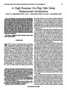
Fig.3 Chip “A” Bus Structure
300
The chip communication pattern for Chip “A” is shown in Fig.3 and an upper wiring layer shown in Fig.4a. The diagonal wiring in Fig.4a also shows a portion of the Chip “A” to Chip “D” interconnections Signal layers, associated with the chip to chip connection, contains wiring parallel to the mesh (in the X,Y directions) and diagonal to the mesh. The nominal impedance is 50 ohms. Due to the high C4 count, breakout from under the chips forces using wiring at a minimum pitch of 200um. To control the impedance and the cross-talk the reference structures are implemented as mesh planes with a 200um pitch in the direction of the parallel inter-chip traces. The diagonal wiring is referenied to a specially constructed mesh plane structure as shown in Fig.4b. This keeps the
imDedance level matched to that of the parallel U
Fig.4a Trace pattern on an upper layer
FigAb Diagonal mesh for impedance control
Electrical Signal Integrity: The bit rate performance of an individual chip to chip net is >5OOMHz (2ns pulse width) Fig. 5 shows the simulation results for an on-module chip to chip path displaying the predicted eye diagram. This eye indicates that there is comfortable margin for future performance enhancement. Volts 1.80 1.70
1.60 1.50 1.40 1.30
1.20 1.10 1.00
0.90 0.80
0.70
0.60 0.50 0.40
0.30 0.20
0.10 -0.00 -0.10
-0.20 -0.30 0.00
0.50
1.00
1.50
2.00
2.50
Fig.5 Eye Diagram at 5OOMHz
301
3.00
3.50
4.00
ns
This bit rate performance is achieved across a very wide set of busses implemented as very dense bundles of interconnections on and off module. The bandwidths available on the different classes of busses are summarized in Table 1.
Table 1: Bandwidth Summary Bus
Bus Frequency
Bandwidth
On Module
> 500 MHz
> 35 GBytedsec.
MCM to MCM
> 500 MHz
> 70 GBytes/sec.
MCM to L3
> 333 M H Z
> 10 GBytes/sec.
Meters of Wire
# of Punched
Meters of Via
# of Signal
# of Module
# of Signal
Via
C4’s
107s
Layers
Total Layers
190
1,771,942
36.64
11,377
5.184
31
71
Conclusion: Utilization of IBM’s HPGC technology with it’s capability to interconnect chips with high bandwidth, high density and deep stacked via capability, results in an interconnection solution with an impressive bandwidth. This bandwidth capacity is facilitated by a unique ring structure designed to promote inter-chip communication. This technique is possible because of IBM’s HPGC ability to support deep stacked via’s both physically and electrically. References:
[ 13 G. Katopis, D. Becker, H. Stoller, “First Level Package Design Considerations for the IBM S1 390 G5 Server”, IEEE EPEP 7th Topical Meeting, pp. 15-16, October 1998. [2] B. V. Fasano, et. al., “Glass Ceramic Substrates for Flip Chip Packages”, SEMICON-WEST, July 1998. [3] R. R. Tummala et. al., “High Performance Glass-Ceramic/Copper Multilayer Substrate With Thin-Film Redistribution”, IBM J. Research & Develop. vo136 no. 5 Sept. 1992, pp889-904.
302