High-Performance Adaption of ARM Processors into Network-on-Chip Architectures Tung Nguyen∗† , Duy-Hieu Bui† , Hai-Phong Phan† , Trong-Trinh Dang∗ and Xuan-Tu Tran† † SIS
Laboratory, VNU University of Engineering and Technology, 144 Xuan Thuy road, Cau Giay, Hanoi, Vietnam. ∗ RMIT Vietnam, Ho Chi Minh city, Vietnam. Corresponding author’s email:
[email protected]
Abstract—The demand for system scalability, reusability, and the decoupling between computation and communication have motivated the growth of Network-on-Chip (NoC) paradigm in the recent years. The system design has changed from the computation centric design to the communication centric design. Researchers have proposed a number of NoC architectures. Most of these works focus on network architectures and routing algorithms, however, the interfaces between network architectures and processing units also need to be addressed to improve the overall performance of the system. This paper presents an efficient AXI (Advanced eXtensible Interface) compliant network adapter for 2D mesh Wormhole-based NoC architectures, named AXI-NoC adapter. The proposed network adapter achieves high frequency of 650MHz with a low area footprint (952 cells, approximate to 2, 793µm2 with a CMOS 45nm technology) by using an effective micro-architecture and with zero latency by using the mux-selection method.
I. I NTRODUCTION With the increase in the complexity of electronic systems, the design requirements such as time-to-market, reusability, reliability, testability, along with many difficult design constraints in performance, power consumption and variability lead to a new design methodology. The Network-on-Chip (NoC) paradigm has been emerging as a promising solution to satisfy the communication needs for high performance designs in the future System-on-Chips (SoCs) [1]–[3]. In NoC architectures, the main components are routers, interconnection links, and network interfaces. The IP cores are connected to the network using the network interfaces. Unlike bus-based method, NoCs are router-based communication networks implemented packet switching communication among IP cores in the network. At each node, before being transmitted on the network, messages are split into many successive packets. Each packet, itself, consists of a number of control/data units (so called flits). It is led by a header flit which stores routing information and followed by other control/data information. The router-based network enables the communication infrastructure as well as IP modules to be easily reused. Different reusable IP cores may not be developed to compatible with the NoC; therefore, a network adapter is needed to provide the interface between the IP core and its associated router. The development of a network adapter allows the IP cores and the communication infrastructure to be independently developed, achieving the decoupling between the computation and communication. The
challenge of deploying the network adapter is the increase of the complexity, area, latency, and the reduction of the maximum frequency [4]. Researchers have proposed a number of NoC architectures. Most of these works focus on network architectures and routing algorithm, however, the interfaces between network architecture and processing units also need to be addressed to improve the overall performance of the system. A network adapter implementing the standard socket was developed to comply with the Æthereal NoC in [5]. However, the forward latency of the network adapter is quite high. In [6], an OCPcompliant adapter for the Xpipes NoC was presented. In [7], a network adapter between clocked OCP bus protocol and an asynchronous MANGO NoC was addressed. In [8], the paper presents an OCP compliant NoC adapter for 2D mesh NoCs. In this paper, we present an AXI-compliant network adapter for 2D mesh Wormhole-based NoCs. Our network adapter, named AXI-NoC adapter, operates as a bidirectional bridge during the data transfer between an ARM processor and the NoC switching fabrics. The AXI-NoC adapter is implemented to support both AXI read and write burst transactions with different configurations of burst length, burst size and burst type. The network adapter also supports source routing algorithms and package switching with Wormhole communication mode. Our main contribution is an efficient micro-architecture for network adapter with low area footprint and high performance. The modularity of the design is also considered to allow easy maintenance and/or further development to support different standard socket protocols. To maximize the throughput and reduce the latency of the network adapter, a mux-selection method is applied. During the data transfer, the network adapter becomes transparent to the whole system. The remaining part of the paper is organized as follows. In Section II, the proposed architecture for the AXI-NoC adapter is presented. This section also explains the main contributions of the paper. Section III shows the discussion about the implementation results and the verification of the design. A comparison with the other related works is also presented. Finally, conclusions will be given in Section IV. II. AXI-N O C A DAPTER D ESIGN In this work, we have designed two types of network adapters to implement the synchronization between AXI inter-
faces and the NoC switching fabric, named Master Network Adapter (MNA) and Slave Network Adapter (SNA), as in Fig. 1. The MNA is used to create the connection between a master IP core and the NoC architecture while a slave IP core connects to the NoC router through the SNA. Each network adapter includes two sub-modules: Request Flow and Response Flow.
this structure enables a packet with just one flit by sending the flit with both BoP and EoP equal ‘1’. 1) Request packet format: The request packets, which is sent from a master IP to a slave IP, consist of the write request packets and the read request packets. The packet format for the write request packets and the read request packets are shown in Fig. 2(a) and Fig. 2(b), respectively.
Fig. 1. Master Network Adapter and Slave Network Adapter. (a)
The basic operation of the AXI interface is the burst transaction. The burst-based transactions enable the use of bandwidth more effectively. We have designed a network adapter that supports three AXI burst types: fixed burst, incremental burst, and wrapped burst. In a fixed burst transaction, the address will be the same for every transfer. This type of burst transactions is useful for accessing to FIFO memories. Unlike fixed burst, in incremental burst, the address for each transfer is an increment of the previous transfer address, and the address just need to be issued once with the read or write request. The incremental burst is suitable for writing/reading to/from a large array of memories. The wrapped bursts operate in the same manner as the incremental bursts, but when a boundary is reached, the address wraps around to the lower address. The network adapter is also designed to support transactions with the burst length varying from 1 to 16 transfers, and the burst size from 1 to 4 bytes. Our AXI-NoC adapter supports the source routing algorithm with Wormhole commutation mode, in which the path from the source node to the destination node is fixed. In the NoC architecture [9], the basic data unit is packet, and it is further divided into flits. There are two types of packets: the request packet and the response packet. A request packet is sent from the source to the destination. The destination responses to that request packet by generating a response packet. The following subsections will describe the packet formats used in our design. A. Packet format Each packet contains one header flit, followed by several body flits and one tail flit. Each flit has a size of 34 bits: 32 bits are used for data, and two most significant bits (“BoP” and “EoP” – standing for “begin of packet” and “end of packet”, respectively) are added for the control purpose. BoP and EoP give information to determine whether the incoming flit is the header flit (BoP = ‘1’, EoP = ‘0’), the body flit (BoP = ‘0’, EoP = ‘0’), or the tail flit (BoP = ‘0’, EoP = ‘1’). In addition,
(b) Fig. 2. Request packet formats: Write request packet (a); and Read request packet (b).
The header flit of the request packet includes the burst length, the burst size, the burst type, the source node, and path-to-target which conforms to the NoC packet header. The source node field in the header flit is the current node that the master IP core is attached to. This information is used by the slave IP core to calculate the return path for the response packet. When the master IP core issues a read or write request to a slave, the network adapter calculates the “path-to-target” based on the destination address and puts it in the header flit of the request packet. The first body flit is used to transfer the destination address of the request. The system uses 32bit address. The address is further divided into global address and local address. The 4 most significant bits in the address are used for the global address which determines the node to which the IP is attached. The remained bits are the local address of the IP. For the read request packet, data is not required; therefore, it needs only two flits, and the tail flit contains the destination address of the packet. 2) Response packet format: The formats of the read response packets and the write response packets are given in the Fig. 3(a) and Fig. 3(b), respectively. When a slave IP core receives a read request, the network adapter uses the source node field in the read request packet to determine the “path-to-target”, and then adds it to the header of the read response packet. While the write response packet,
(a)
(b) Fig. 3. Response packet formats: Read resonse packet (a); and Write response packet.
which does not require data, has only one flit (BoP = ‘1’, and EoP = ‘1’). The proposed MNA architecture is presented in the next subsection. Since the SNA is similar and less complex than the MNA, therefore, the design of SNA is not presented in this paper. B. Master Network Adapter The MNA encapsulates requests from the master core into NoC packets. It also decapsulates responses from the router and transfer it to the AXI master. The MNA mainly composes of two data flows: MNA Request Flow and MNA Response Flow, which are responsible for encapsulation and decapsulation (Fig. 4).
Fig. 4. MNA Architechture.
1) MNA Request Flow: The MNA Request Flow consists of two main modules: MNA Flit Builder and MNA Transmitter, as shown in Fig. 5. The left hand side signals are the interface with the master IP core, the right hand side signals are the interface to the router of the NoC. The purpose of the MNA Flit Builder module is to form the flits for the request packets from the AXI master burst transactions. The BoP and EoP are automatically added to the flits. This module implements a look-up table to calculate the “path-to-target”. The inputs of the look-up table are the 4most significant bits in the address bus. The outputs of the
Fig. 5. MNA Request Flow architecture.
Flit Builder module are 34-bit header, which is the header flit of request packet, ‘sub header’, and ‘wdata i’. In a write burst transaction, ‘sub header’ is the first body flit, and ‘wdata i’ contains the remain flits of the write request packet. In a read burst transaction, ‘sub header’ is the tail flit. The MNA Transmitter module manages the sequence of flits created by MNA Flit Builder module to be sent to the network (the header flit → the body flit(s) → the tail flit), and to control the handshaking signals to the AXI master address channel and the write data channel. The operation of the MNA Transmitter module is based on a Finite State Machine (FSM). Depending on the current state, the data output to the network ‘pdata to noc’ (packet data to be sent to the NoC) will be ‘header’, ‘sub header’, or ‘wdata i’ which are from the MNA Flit Builder module. The MNA Transmitter module will select the appropriate flits to be sent to the network. Hence, the number of states is reduced, and the FSM is much simpler. To increase the network adapter’s performance in terms of throughput and latency, we proposed a mux-selection method to optimize the design. The mux-selection method is the combination of using FSM technique and implementing of the additional MUXes to control handshaking signals at both sides of the interfaces. In Fig. 6, two MUXes are added to control the output signals of the network adapter, which are the request signal (‘pvalid to noc’) to send data to the destination interface, and the response signal (‘wready’) accepting data from the source interface (AXI). Thanks to this arrangement, ‘wready’ and ‘pvalid to noc’ signals are controlled by the FSM or they output the value of ‘wvalid’ signal directly depending on the value of ‘hs sel’ signal (handshake selection). Fig. 6(b) presents the finite state machine of the MNA Transmitter. As the handshaking signals are controlled by the FSM, this method has the advantages of the FSM based handshaking method described in the previous subsection. The state transition is easily managed by the FSM to ensure the proper operations. The mux-selection method provides a way to directly control the output signals of the network adapter. This structure allows data at the AXI interface to appear at the NoC interface intermediately resulting in the zero latency in the data transfer.
MNA Request Flow, the proposed mux-selection method has been also applied for MNA Response Flow to improve the performance. The optimized block diagram of MNA Response Flow and its finite state machine are shown in Fig. 7.
(a)
(a)
(b) Fig. 6. MNA Transmitter module: Optimized micro-architecture (a); and Finite State Machine (b).
When the MNA Transmitter module is in the state of ready to accept data from the AXI interface, and the NoC is ready to receive a new packet, the data is sent to the NoC at the same clock cycle which the data on the AXI interface is available. If the NoC is not ready, the data at AXI interface are buffered until there is a response from the network. 2) MNA Response Flow: The structure of the MNA Response Flow module is much simpler than that of the MNA Request Flow module. The network is the source, and the master core is the destination of the MNA Response Flow. The packets from the network are decapsulated at AXI interface. The MNA Response Flow manages data transfers to the appropriate channel. When a packet is valid at the router (‘pvalid fr noc’ is high), the MNA Response Flow reads the header flit to determine whether it is a read response packet or a write response packet. In the case of write response packet (the packet has only one flit), the MNA Response Flow extracts the information of the header flit and sends it to the AXI write response channel of the master core. If it is a read response packet (the header flit → the read data (1) → . . . → the read data (n-1) → the tail flit (the read data (n))), the read data will be transferred to the AXI read data channel. ‘rlast’ signal is high when the tail flit of a read response packet is received. This indicates the last data transfer. Similarly to the
(b) Fig. 7. MNA Response Flow module: Optimized micro-architecture (a); and Finite State Machine (b).
III. I MPLEMENTATION AND V ERIFICATION The AXI-NoC adapter design has been modelled in VHDL at RTL level and implemented using a CMOS 45nm technology. It requires a low area cost compared to the NoC routers (less than 10% area cost of a network router in our case). Fig. 8 presents the relationship between power consumption (in mW ), area cost (in µm2 ) versus the (synthesized) operating frequency of the design. The design is able to achieve a maximum operating frequency of 650MHz. At 650MHz, the area cost of the design is about 952 cells and the total cell area is about 2, 793µm2 . The design can achieve a communication throughput of 2.6GBytes/s, and the network adapter consumes approximately 4.14mW . Table I shows a brief comparison of our work with some related works including [5], [10], [11], and [12]. It is clear from the table that our work achieves the highest performance
TABLE I I MPLEMENTATION RESULTS IN COMPARISON WITH THE RELATED WORKS [5] Target bus interface
[10]
[11]
[12]
This work
OCP/AXI/DTL
OCP
NA
OCP/AXI/Wishbone
AXI
Technology
0.13µm
0.13µm
0.18µm
90nm
45nm
Max frequency
500MHz
400MHz
457 − 490MHz
NA
650MHz
0.143
0.02-0.064
0.055-0.103
0.024
0.0028
Area (mm2 ) Power (mW) Latency (with packetization) Throughput
NA
NA
19.5-44.0
NA
4.41
4-10 cycles
3-8 cycles
NA
NA
1
16Gbit/s
NA
NA
NA
20.8Gbit/s
in terms of operating frequency, processing delay and communication throughput. Our design can operate at 650M Hz with 45nm technology while the others have the maximum frequencies in the range from 400M Hz to 500M Hz but with the older technologies. The occupied area of our work is ten times smaller in comparison with the work presented in [12]. The notable results in our work are the processing latency and the communication throughput. With the applied techniques, our design has no processing latency and the highest communication throughput when comparing with [5]. The limitation of our work is to support only AXI interfaces while [5] and [12] support multiple bus protocols. Fig. 9. Vefification environment with 9 network routers.
Fig. 8. Power consumption and area cost at targeted frequencies.
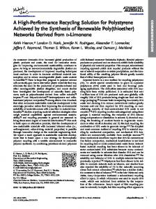
To verify the proposed AXI-NoC adapter architecture, we have developed a 2D mesh NoC test environment as shown in Fig. 9. This environment includes 9 network routers, 8 IPs, 1 ARM model connected to the associated network router by using the Master Network Adapter. The dummy IP models (IP0 to IP7) are simple IPs that can generate NoC packets and response to incoming NoC packets. These dummy IPs act like simple memory models. When receiving a write request packet, dummy modules store write data to its internal memory. When receive a read request, it extracts information of the request packet to calculate the return path for the response packet; then, dummy IP sends stored data to the node where the request packet is issued. The ARM model is configured to generate both read and write burst transactions with different settings of burst types, burst lengths, and burst sizes. Timings at both sides of the
Master Network Adapter are observed. The response data to the ARM model are compared with the expected results. Each test case goes through several steps. Firstly, random data are generated. Secondly, the ARM model issues a write burst request to a dummy IP with the generated data in step 1. Then, a read burst is issued to the same location as in step 2. Finally, the read data are compared with the data that has been written. In short, we do write to and read from the same location. The write data and the read data must be identical. Fig. 10 presents the layout of the MNA design.
Fig. 10. The final layout of the design.
IV. C ONCLUSIONS In this paper, we have presented the AXI-NoC adapter, which is used to adapt ARM cores into Network-on-Chip architectures. The network adapter acts as a bi-directional bridge between AXI interface and the NoC architectures. It supports the source routing algorithm, Wormhole-switching communication mode. In terms of the AXI interface specifications, both read burst and write burst transactions are supported. One of the advantages of the AXI-NoC adapter is that it offers a simple network adapter architecture, which requires low area footprint to implement the design (about 2793µm2 ) and achieves a high throughput of 2.6GBytes/s. Another advantage of the design is the usage of the muxselection method to decide whether the outputs to one-side interface are controlled by the state machine or directly by the input handshaking signals from the other side. This method reduces the latency to zero and therefore improve the overall performance of the system. The AXI-NoC adapter can be used to connect other IPs conforming to the AXI specifications to NoCs. ACKNOWLEDGMENT This work is supported by the research project “Reconfiguration Solution in Designing Network-on-Chip Architectures” granted by Vietnam National Foundation for Science and Technology Development (Nafosted) and by the research project No. QGDA.10.02 (VENGME) granted by Vietnam National University, Hanoi (VNU). The authors would like to thank the Nafosted for travel grant. R EFERENCES [1] W. Dally and B. Towles, “Route packets, not wires: On-chip interconnection networks,” in Proceedings of the 2001 Design Automation Conference, 2001, pp. 684–689. [2] K. Goossens, J. Dielissen, and A. Radulescu, “Æthereal network on chip: Concepts, architecture, and implementations,” IEEE Design & Test of Computers, vol. 22, pp. 414–421, 2005.
[3] S. Pasricha, N. Dutt, and M. Be-Romdhane, “BMSYN: Bus matrix communication architecture synthesis for MPSoC,” IEEE Transactions on Computer-Aided Design of Integrated Circuits and Systems, vol. 26, pp. 1454–1464, 2007. [4] B. Attia, W. Chouchene, A. Zitouni, and R. Tourki, “Network interface sharing for SoCs based NoC,” in Proc. 2011 Int’l Conference on Communications, Computing and Control Applications, 2011, pp. 1–6. [5] A. Radulescu, J. Dielissen, K. Goossens, E. Rijpkema, and P. Wielage, “An efficient on-chip network interface offering guaranteed services, shared-memory abstraction, and flexible network configuration,” in Proceedings of the 2004 Design, Automation Test in Europe Conference Exhibition (DATE), 2004, pp. 878–883. [6] S. Stergiou, F. Angiolini, S. Carta, L. Raffo, D. Bertozzi, and G. De Micheli, “Xpipes lite: a synthesis oriented design library for networks on chips,” in Proceedings of the 2005 Design, Automation Test in Europe Conference Exhibition (DATE), 2005, pp. 1188–1193. [7] T. Bjerregaard and J. Sparso, “A router architecture for connectionoriented service guarantees in the MANGO clockless network-onchip,” in Proceedings of the 2005 Design, Automation Test in Europe Conference Exhibition (DATE), 2005, pp. 1226–1231. [8] B. Attia, A. Zitouni, N. Abid, and R. Tourki, “A modular network interface adapter design for OCP compatibles NoCs,” International Journal of Computer and Network Security, 2009. [9] N.-K. Dang, T.-V. Le-Van, and X.-T. Tran, “FPGA implementation of a low latency and high throughput network-on-chip router architecture,” in Proceedings of the 2011 International Conference on Integrated Circuits and Devices in Vietnam (ICDV), 2011, pp. 112–116. [10] T. Bjerregaard, S. Mahadevan, R. Olsen, and J. Sparsoe, “An OCP compliant network adapter for GALS-based SoC design using the MANGO network-on-chip,” in Proceedings of the 2005 International Symposium on System-on-Chip, 2005, pp. 174–174. [11] D. Matos, M. Costa, L. Carro, and A. Susin, “Network interface to synchronize multiple packets on NoC-based systems-on-chip,” in Proceedings of the 18th IEEE/IFIP VLSI System on Chip Conference (VLSI-SoC), 2010, pp. 31–36. [12] J. Sparso, E. Kasapaki, and M. Schoeberl, “An area-efficient network interface for a TDM-based network-on-chip,” in Proceedings of the 2012 Design, Automation Test in Europe Conference Exhibition (DATE), 2010, pp. 31–36.