High-performance ASIC Implementations of the 128-bit Block Cipher CLEFIA Takeshi Sugawara, Naofumi Homma, Takafumi Aoki
Akashi Satoh
Graduate School of Information Sciences, Tohoku University, Sendai, Miyagi, Japan {sugawara, homma}@aoki.ecei.tohoku.ac.jp
[email protected]
National Institute of Advanced Industrial Science and Technology, Research Center for Information Security, 1-18-13, Sotokanda, Chiyoda, Tokyo, 101-0021, Japan
[email protected]
Abstract— In the present paper, we introduce high-performance hardware architectures for the 128-bit block cipher CLEFIA and evaluate their ASIC performances in comparison with the ISO/IEC 18033-3 standard block ciphers (AES, Camellia, SEED, CAST-128, MISTY1, and TDEA). We designed five types of hardware architectures for CLEFIA, combining two loop structures and three F-functions. These designs were synthesized with a 90-nm CMOS standard cell library, and size and speed performances were evaluated. The highest hardware efficiency (defined as throughput/gates) obtained was 400.96 Kbps/gates, which is 1.5 times higher than previously achieved efficiencies.
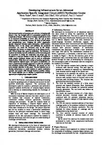
GF(28) and an affine transformation similar to AES and Camellia. The S-box S0 is defined as a combination of four 4bit input/output S-boxes (SS0 ~ SS0) and constant multiplications over GF(24).
I.
INTRODUCTION
CLEFIA is a 128-bit block cipher developed by SONY Corporation [1]. Previous studies [2, 3] reported that CLEFIA has the advantages of speed and size in hardware implementation, as compared to conventional algorithms, and a throughput of over 1.6 Gbps with less than 6 Kgates was achieved in a 90-nm CMOS standard cell library. However, in these studies, other block ciphers were not implemented, and the 90-nm library used was more advanced than libraries used in other studies on hardware implementation of block ciphers. Therefore, the advantage of CLEFIA hardware remains unclear. In the present paper, we present high-speed and compact datapath architectures for CLEFIA. In addition, we applied various optimization techniques to each basic function block. Five architectures combining these methods were then synthesized using a 90-nm CMOS standard cell library with speed and area optimization options. We also designed and synthesized all of the ISO18033-3 standard block ciphers (AES, Camellia, SEED, CAST-128, MISTY1, and TDEA) [4] in order to fairly compare their performances with CLEFIA under the same conditions. II.
The key scheduler block of CLEFIA is shown in Figure 2. Round keys RKi are generated by XORing a secret key K, an intermediate key L, and constant values CONi. The intermediate key L is generated by mixing K and CONi using the GFN. The intermediate key L is updated by a DoubleSwap function Σ, which is defined as a bit-wise permutation. The constant values CONi are defined as a combination of smaller constants T, P, and Q with constant multiplications over GF(216).
A. Compact implementations of S-boxes S0 and S1 A straightforward implementation of S-boxes is based on a lookup table that is automatically generated by synthesis tools.
Plaintext 128 32 WK0
32
F0 32 WK1
RK0
RK1
F0
F1
RK2
RK3
F0
F1
x0
8
S0
x1
8
S1
x2 x3
RK2r-3
F0
F1
RK2r-2
RK2r-1
F0
32
32
128 Ciphertext
Figure 1
8
y0
8
y1 y2
8 8
y3
S1
8
y0
k0 k1 k2 k3 8
S0
8 8
S1
x3
8
S0
4
SS0
×2
M1
y1
8 8
y2
8
y3
SS2
4
SS3
4
affine g
8
×2 4
WK3 32
8
M0
S1
x2
S0
F1
WK2
S0
8
F1
x1 RK2r-4
k0 k1 k2 k3
32
x0
CLEFIA ALGORITHM
Figure 1 shows a data randomization block of CLEFIA using the Generalize Feistel Network (GFN) structure, which is an n-branch expansion of the Feistel Network. CLEFIA uses a four-branch GFN dividing a 128-bit block into four 32-bit sub-blocks. Two types of 32-bit input/output F-functions, F0 and F1, are used for the data randomization. The F-functions consist of XORs, 8-bit input/output S-boxes, and multiplications by diffusion matrices M0 and M1. The S-box S1 is defined as a multiplicative inverse over a Galois field
OPTIMIZATION OF CIRCUIT COMPONENTS
III.
32
SS1
S1 8
affine f
inversion over GF(28)
Data randomization block
A different type of implementation technique is also available for the S-box S1 using a Galois field arithmetic [5], which considerably reduces the circuit area [2, 3]. The compact implementation of S1 is derived from an inversion over the composite field GF((24)2) transformed from the original field GF(28). The size of S-box S0 can also be reduced by using four smaller S-boxes SS0 ~ SS0 and constant multipliers over GF(24). B. Sharing the diffusion matrices M0 and M1 Permutation functions in F-functions are defined by constant matrices M0 and M1 with elements of {02, 04, 06, 08, 0A} ∈ GF(28). The compact implementations, which only require constant multipliers of {02, 04, 08} ∈ GF(28) and XORs, are proposed in References [2, 3]. In addition, we introduce a further reduction technique to share resources between M0 and M1. Figure 3 shows the linear transformation circuit sharing constant {02} multipliers and XOR gates.
C. Fast implementation using T-boxes T-box is a technique to merge an S-box and following linear transformation layers to shorten the critical path, although it requires large hardware resources. The T-box technique can also be applied to CLEFIA by merging S-boxes S0 and S1 and multiplications by the diffusion matrices M0 and M1. Reference [2] proposed four types of T-boxes considering a trade-off between throughput and hardware cost. For example, the Type-1 T-box consists of 8-bit input 32-bit output tables TB00 ~ TB13 defined by the following equations: TB00(x) = ( S0(x), 02×S0(x), 04×S0(x), 06×S0(x)) TB01(x) = (02×S1(x), S1(x), 06×S1(x), 04×S1(x)) TB02(x) = (04×S0(x), 06×S0(x), S0(x), 02×S0(x)) TB03(x) = (06×S1(x), 04×S1(x), 02×S1(x), S1(x)) TB10(x) = ( S1(x), 08×S1(x), 02×S1(x), 0A×S1(x)) TB11(x) = (08×S0(x), S0(x), 0A×S0(x), 02×S0(x)) TB12(x) = (02×S1(x), 0A×S1(x), S1(x), 08×S1(x)) TB13(x) = (0A×S0(x), 02×S0(x), 08×S0(x), S0(x)) The S-boxes and the linear transformations in CLEFIA can be executed using TB00 ~ TB13 and XORs. D. On-the-fly CONi generation The constants CONi require several memory element (e.g., registers or memory modules) if they are computed and stored in advance. For more details, CON1 ~ CON60 requires 1,920 bits (= 32 bits × 60). Even if we store the smaller constants T1 ~ T30 instead of CONi, 480 bits (16 bits × 30) are required. Therefore, on-the-fly CONi generation is quite effective for reducing the hardware resources. Figure 4 shows a schematic diagram of the on-the-fly CONi generator, which consists of a PQ operator, which generates CONi from Ti, and two constant multipliers where the constants are 2, 2-1 ∈ GF(216). Register T stores the value of Ti updated by the constant multipliers on the fly. 16-bit constants IV, T12, and T29 are used to reset the value in register T. IV.
Figure 2
Figure 3
Key-scheduling block
Linear transformation circuit for multiplications by M0 and M1
CIRCUIT ARCHITECTURES
Figures 5 and 6 show the proposed datapath architectures with the above-described component optimizations. The TypeA architecture in Figure 5 executes one round operation in one clock cycle, while the Type-B architecture in Figure 6 performs one round operation in two clock cycles. These architectures support both encryption and decryption in the ECB mode with a 128-bit key. Therefore, both Type-A and Type-B architectures require 18 and 36 clock cycles,
Figure 4
On-the-fly CONi generator
respectively, for one-block encryption (or decryption). The intermediate key L is generated by the data randomization block. The encryption (or decryption) processes can be executed continuously without any interval cycles. In both architectures, we implemented two types of S-boxes: the lookup table and composite field versions described in Section III-A. In addition, the T-box described in Section III-C was also applied to the Type-A architecture. Round keys RKi are computed and stored in an internal register one clock prior to use, which enables the reduction of the critical path. We also reduce the number of selectors using the functions Ω, Ψ, and Φ, rather than the DoubleSwap function Σ, as described in [4]. In the Type-B architecture, we designed an F0/F1 component combining F-functions F0 and F1, where we shared the S-boxes as well as the constant matrices M0 and M1, as described in Section III-B. In addition, the circuit area for the component PQ is reduced by sharing XOR gates. PERFORMANCE EVALUATION IN ASIC
V.
Table I shows the synthesis results of the Type-A and Type-B architectures using the STMicroelectronics 90-nm CMOS standard cell library (1.2V-volt version) [6]. The designs are synthesized by a Synopsys Design Compiler with two optimization options: size and speed. Hardware sizes were estimated based on a two-way NAND equivalent gate, and the speeds were evaluated under the worst-case conditions. The efficiency is defined as the throughput per gate, and thus higher efficiency indicates better implementation. For the comprehensive performance comparison of block ciphers, we also designed all of the ISO standard algorithms AES, Camellia, SEED, CAST-128, MISTY1, and TDEA [4] and evaluated their sizes and speeds under the same condition. A compact AES implementation [7] with a 0.13 μm library is also shown in Table I.
by the Type-A architecture with compact S-boxes. This value was more than twice as high as that of AES (175.72 Kbps/gates), which is the highest value among the ISO standard ciphers. The highest throughput of 5.31 Gbps was achieved in the Type-A architecture with the T-box, but the efficiency remained low due to the large T-box circuit. The throughput was lower than the value of 7.31 Gbps achieved by AES because the Feistel-type CLEFIA requires 18 rounds while the SPN-type AES takes 10 rounds. The Type-B architecture achieved a circuit area of 5.49 Kgates, which is the smallest among all of our CLEFIA implementations. AES in [7] has a smaller circuit area of 3.10 Kgates, but it does not support decryption and its efficiency is much lower than that of our Type-B even if the difference in circuit technology is considered. On the other hand, the circuit area of 5.49 Kgates for Type-B with compact S-box is only 9% smaller than that of 6.05 Kgates for Type-A with the compact S-box. This result indicates that the F0/F1 merged technique has a limited effect on area reduction because the size of additional selectors is not negligible. Compared with References [2] and [3], the present circuit has a higher throughput but a larger circuit area. This is due to the design strategy of the present study of prioritizing the shortening of the critical path compared to the reduction of the circuit area. As a result, we improved the efficiency and the throughput by 50% and 75%, respectively, as compared to the designs reported in References [2] and [3]. VI.
CONCLUSION
In the present paper, we proposed high-performance hardware architectures for the 128-bit block cipher CLEFIA,
Data in 128
The highest efficiency of 400.96 Kbps/gate was obtained
K
L
128
128 64
WK
Ω
Ψ
Φ
IV 16
L 4:1
128
2:1
32
K
Ω
64
Ψ
Φ
32
64
L 128
32
16
64
CON 64
16
L
16
PQ
×2
Data Out
×2
17
×2
F0/F1
S0
L
-17
×2
32
WK
Figure 6
S1 8 S0 S1
128
Data out
Type-A architecture
×217
32
Switching Box
64
WK
Figure 5
32
32 -1
×2
RK
64 32
RK
128
×2-1
IV
T
F1