subsystems including source, optics and performance specifications are given. ..... For enabling tool testing without the use of a track an additional load lock was ...
High-resolution EUV Microstepper tool for resist testing & technology evaluation A Brunton, J Cashmore, P Elbourn, G Elliner, M Gower, P Grünewald, M Harman, S Hough, N McEntee, S Mundair, D Rees, P Richards, V Truffert, I Wallhead, M Whitfield Exitech Ltd, Oxford Industrial Park, Yarnton, Oxford OX5 1QU, England
ABSTRACT Key features are presented of the Exitech MS-13 EUV Microstepper tool developed for EUV resist testing & technology evaluation at the 32nm node and beyond. Details of the tool design architecture, module layout, vacuum chamber, major subsystems including source, optics and performance specifications are given. Key Words: EUV lithography, Microsteppers
1.
INTRODUCTION
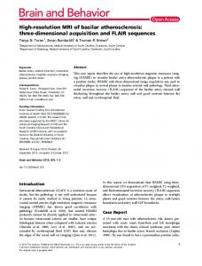
Using a reduced image field size at a similar optical resolution to that eventually intended to be adopted in production, the semiconductor industry uses Microsteppers to gain early learning on new technology nodes four to five years ahead of their introduction. Microsteppers allow manufacturers and researchers alike to develop and qualify new photoresists well ahead of when they are required for volume IC manufacturing. For example, processing an average of 50 wafers and 5-15 resist formulations a day since June 2000, the 157nm, 0.85NA, 15x reduction, 0.7mm field diameter Exitech MS157 Microstepper at the Resist Test Center of International SEMATECH (ISMT) has been a workhorse for the industry in qualifying 157nm F2 laser lithography for manufacturing to the 45nm node. Microsteppers also allow researchers to investigate defect printability, test new reticle designs and fabricate prototype IC’s at the node of interest as well as providing early learning on tool-related technology challenges associated with for example sources, optics, lens aberrations, imaging effects, materials, metrology, reticles, pellicles, photoresists, contamination, tool cost of ownership, reliability and lifetime. Main tool exposure chamber Reticle access
Wafer track
EUV source Xe discharge Z-pinch 35W/2
Wafer load robot & wafer prealigner Turbo molecular pump 3,000l/sec Wafer stage access
Figure 1. MS-13 EUV Microstepper architecture.
This paper describes key features of the Exitech MS-13 Microstepper, the world's first commercial high-resolution EUV exposure tool. The tool whose architecture is shown in Figure 1, is developed for EUV resist testing, technology evaluation and early learning at the 32nm node and beyond. Operating in a step-and-repeat exposure mode, the tool is
capable of printing x5 de-magnified high-resolution features from 6" EUV reflective reticles onto 200 or 300mm diameter wafers over an image field die size of 0.6x0.2mm. Exposures times for a 10mJ/cm2 sensitivity photoresist are around 0.25sec/die. Details of the tool design architecture, module layouts, high vacuum chamber, major subsystems including performance specifications are presented below.
2. EUV TOOL CONCEPTS When imaging the same feature sizes with EUV or DUV photons the greater than tenfold reduction of EUV wavelength allows an equivalent reduction to be made to the mask imaging numerical aperture (NA) which in turn leads to almost an equivalent increase in the depth of focus (DOF) of the image. Making incremental increases to imaging NA provides EUV lithography (EUVL) with the resolution capability of covering many nodes beyond 32nm. Between 1997–2002 EUVL was given a tremendous technology push by developments made by the EUV Limited Liability Company (EUV LLC) - a consortium formed by IC manufacturers AMD, IBM, Infineon, Intel, Micron and Motorola. By building relatively low numerical aperture (0.1NA), x10 microstepper and x4 full-field scanner systems (the Engineering Test Stand) and providing access to their exposure capabilities, work carried out by the EUV LLC at the Virtual National Laboratory (Lawrence Livermore, Sandia and Lawrence Berkeley National Laboratories) did much to establish the credibility of EUVL. The EUV LLC also provided valuable early learning in areas such as EUV source development, optics and coating fabrication, high accuracy interferometry and tool related issues such as contamination, EUV reticle and wafer handling. In developing the MS-13 Exitech licensed the intellectual property and the more than 100 related patents owned by the EUV LLC. Since all solids, liquids and gases are highly opaque to EUV radiation at 13.5nm, the source, beam delivery, imaging objective, reticle, wafer handling and stages in the tool must operate in a vacuum environment. Reflective rather than refractive optics must be used for optical beam transport, shaping and imaging. Normal incidence mirrors can be fabricated using phase-additive reflections from up to 100 layers of silicon and molybdenum (magnetron, ion or electron beam deposited) each only 3nm or about 15 atoms thick. Reticles themselves must be reflective with circuit features now defined by patterning a thin absorbing layer on top of the reflective multilayers. To replace the vacuum chucking methods used in more traditional atmospheric pressure DUV steppers, new techniques for wafer and reticle stage clamping must be developed compatible with an overall vacuum environment. Because EUV radiation is very aggressive at cracking most molecular species the products of which can contaminate and erode sensitive optical coatings, any hydrocarbons or water vapour in the vacuum chamber must be minimized. This requirement necessitates the tool chamber to have the cleanliness of an ultra-high vacuum (UHV) system. Since all highpower EUV sources are currently based on plasmas (laser-produced or gas discharge pinches), the potential for further optics contamination can also arise from the inherent heavy particle and charged ion debris such sources produce. Source debris must be contained by trap arrangements and kept well away from the imaging section of the tool. This is particularly difficult since a EUV source must be engineered to be integral to the tool body rather than being remote from it like an excimer laser source is with a DUV stepper. With most of their input energy converted to waste heat, incoherent EUV plasma-based sources are much less efficient generators of radiation than DUV excimer lasers. Efficient thermal management of excess heat from the source in both its radiative and conductive forms as well as effective damping of any source mechanical vibration are required if the ultimate imaging performance of the tool is to be achieved. Unlike DUV tools operating at atmospheric pressure, the high vacuum chambers required for EUV stepper operation make subsystems inaccessible for simple maintenance and servicing. A high degree of subsystem automation of appropriate vacuum, radiation, position and motion control together with their diagnostics are required to maintain tool functionality and serviceability. Compared to 248nm, 193nm and 157nm DUV exposure tools, the EUV spectral region at 13.5nm wavelength presents many complex challenges to the exposure tool builder which require entirely new engineering concepts be developed.
2. EUV SOURCE The Xe gas discharge Z-pinch plasma illumination source used in the MS-13 is shown in Fig. 2(a) and is manufactured by Xtreme Technologies GmbH. Its electrode structure is shown in Fig 2(b). At 1kHz repetition rate, approximately 3kW of radiation at all wavelengths is emitted by the source into 2L steradians of which 35W is contained within 2% bandwidth of the EUV wavelength at 13.5nm. Bursts of pulses with a duty cycle typically between 2-10% are used for resist exposures. The pulse-to-pulse stability of the EUV radiation from the source as measured at the reticle plane in the
MS-13 is shown in Fig 2(c). As can be seen, after relaying to the reticle by the collection and relay optics in the tool the 3x standard deviation (3N) of the EUV pulse intensity is 18.0%.
(a)
(c) (b) Test Data for Specification 8.1 Source Power Measurement (at Q2 quad dose sensor) (sigma 0.36 - 0.55) 3
= 18.0%
0.006
2
Dose(mJ/cm )
0.005 0.004 0.003 0.002 0.001 0 0
2000
4000
6000
8000
10000
Pulse Count
(a) (c) Figure 2. (a) EUV Z-pinch Xe gas plasma source (b) electrode structure of pinch (c) Pulse-to-pulse EUV power measured for 10,000 pulses at the MS-13 reticle plane. Rep rate = 1kHz, 2% duty cycle; Bursts of 250 pulses. 3N deviation: 18.0%
3. EUV OPTICS 3.1 EUV imaging objective High-resolution imaging in the MS-13 Microstepper is accomplished using a 0.3NA, x5, 600x200µm field size objective of a two-mirror aspheric design developed by the EUV LLC under a contract from International SEMATECH. The objective and other elements of the EUV optical train are manufactured by Carl Zeiss SMT. The lens and its key parameters are shown in Figure 3. Wavelength Numerical aperture Form Field size at wafer Demagnification Mag anisotropy Track length Wavefront error - design - manufactured Straylight Minimum CD Usable DOF CD uniformity H-V bias Linearity TFPD Astigmatism Outgassing rates
13.54nm . Fit to 6° CRA reticles @ 13.5nm 0.3 2 mirror aspheric design 0.6 x 0.2mm 5x 10⁻³ due to reticle tilt T 0.031 rms (0.42nm)