mechanism involved in the fief carrier absorption process can be due to phonon scattering @d/or impurity scattering. For n- and p-type Si, if we choose the ...
Homojunction performance
internal analysis
photoemission
far-infrared
detectors:
Photoresponse
A. G. U. Perera, H. X. Yuan, and M. H. Francombe Department of Physics and Astronomy, Georgia State University, Atlanta, Georgia 30303 (Received 16 May 1994; accepted for publication 5 October 1994) The concept of homojunction infernal photoemission far-infrared (FIR) detectors has been successfully demonstrated using forward biased Si p-i-n diodes at 4.2 K. The basic structure consists of a heavily doped IR absorber layer and an intrinsic (or lightly doped) layer. An interfacial workfunction between these regions defines the long-wavelength cutoff (X,) of the detector. Three types of detectors are distinguished according to the emitter layer doping concentration level. Our model shows that high performance Si FIR detectors (>40 pm) can be realized using the type-II structures with a tailorable X,, in which the absorber/emitter layer is doped to a level somewhat above the metal-insulator transition value. Analytic expressions are used to obtain the workfunction versus doping concentration, and to describe the carrier photoemission processes. The photoexcitation due to free-carrier absorption, emission to the interfacial barrier, hot-carrier transport, and barrier collection due to the image force effect, are considered in calculating the spectral response and quantum efficiency as functions of device parameters for Si n+ -1’ structures, leading to a detailed photoresponse analysis of type-II detectors. These results are useful for the design and optimization of type-II detectors. 0 1995 American Institute of Physics.
I. INTRODUCTION In recent years, there has been a great need to develop far-infrared (FIR) detectors for space astronomy applications, such as the Space Infrared Telescope Facility (SIRTF).’ The conventional detectors used for the 40-200 ,um wavelength range are extrinsic Ge photoconductors, such as unstressed Ge:Ga devices for the 40-120 ,um and stressed Ge:Ga for the 120-200 pm.2 Ge blocked-impurityband (BIB) detectors3V4are also under development in order to overcome the limitations inherent in conventional extrinsic photoconductors and extend the cutoff wavelength (X,) . However, at present, no Si FIR detectors exist that can operate effectively beyond 40 pm at ‘low backgrounds.5 In this paper, we present an analytic model for a novel Si homojunction internal photoemission FIR detector, with high performance and a tailorable X, . The concept of homojunction internal photoemission for FIR detection was first proposed ‘and demonstrated on forward biased commercial Si p-i-n diodes at 4.2 K.6 The detector X, was extended to very long wavelength range (>200 pm), and similar results were also obtained for Ge and InGaAs p-i-n diodes.7 In addition, experimental results obtained with a single p ‘-i interface structure were reported, and the concept of multilayer structures was proposed.* Also, similar detector concept was proposed and demonstrated for a Si molecular beam epitaxy (MBE) multilayer structure in the LWIR range.” The detection mechanism6 assumes that the biased interface structure, consisting of a heavily doped IR absorber layer and an intrinsic (or lightly doped) layer (n ‘-i or p+-i), can be depicted as an internal photoemitter at low temperatures (s20 K). For an y1‘-i (p’-i) structure, the Fermi level in the heavily doped layer can lie below (above) the conduction (valence) band edge of the i layer, giving rise to an interfacial workfunction, which defines the longwavelength IR cutoff for the detector. When the doping conJ. Appl. Phys. 77 (2), 15 January 1995
0021-8979/95/77(2)/915/l
centration is above the metal-insulator transition (Mott transition) value, the detector can be regarded as a metal photoemitter, which will be called type-II detector in this paper, otherwise it can be regarded as a semiconductor photoemitter (type-I detector). Following a linearly distributed space-charge model,” we can show that the space-charge effect at the interface is negligible at low temperatures. As all the experimental results, up to now, were obtained on commercial p-i-n diodes which were not designed for IR detectors, detector performance was not high. In order to fabricate detectors with high performance, device parameters should be optimized. This in turn requires a better understanding of the detector photoresponse mechanism and detailed modeling work. The photoresponse mechanism of type-1 detectors has been analyzed in another paper.” In this paper, our focus is mainly on the type-II detector. Up to now, several types of internal photoemission IR detectors have been proposed and demonstrated.12 One important type is metal-semiconductor Schottky barrier IR detectors, such as the most highly developed PtWSi detector13 operating in 3-S pm. Another type is semiconductor heterojunction IR detectors, such as Ge.$i, -,/Si detectors14*‘5 developed for 8-14 pm or even longer wavelength. There is also a degenerate Si homojunction detector,16 which has a response in l-7 pm. Since the structure of the latter detector is very similar to the detectors investigated in this work, here it is categorized as the type-III. In these detectors, the absorber/photoemitter Lielectrode” may be a metal, a metal silicide or a degenerate semiconductor. Thus, following the terminology of Lin and Maserjian,14 we may describe all of these detectors as HIP, i.e. hetero- (or homo-j junction internal photoemission detectors. The actual physical processes taking place in the emitting layer are still not well understood, although several theoretical models17-2’have been developed to describe the hot carrier photoemission. Some of these models will be followed here, to predict the photoreO/$6.00
Q 1995 American Institute of Physics
915
Downloaded 10 Oct 2001 to 131.96.4.38. Redistribution subject to AIP license or copyright, see http://ojps.aip.org/japo/japcr.jsp
sponse performance of our type-II HIP FIR detectors. One of the key factors for the design of type-II HIP detectors is to determine the doping concentration dependence of the inter-facial workfunction (hence 1,). The heavy doping effects on semiconductor properties, such as the band-gap narrowing, have been extensively studied, from both theoretical and experimental respects.“2 But the physical mechanism is not yet well understood. Also, there is no experimental data available at present time describing the workfunction dependence on doping concentration above the Mott transition. In this paper, we will follow a theoretical model= developed recently, which can give simple but accurate closed form equations for band-gap narrowing, to obtain an approximate relationship of h, vs doping concentration for the type-II HIP detector. This paper is arranged in the following way. In Sec. II, three different types of HIP detectors are compared; In Sec. III, an estimate of the workfunction dependence on the doping concentration above the Mott transition is given. In Sec. IV, an analytic model is introduced to describe the carrier photoemission in single layer (n+-i or p f -i) type-II HIP detectors, which includes photoexcitation, emission to the interfacial barrier, hot electron transport, and barrier collection. In Sec. V, the spectral response and quantum efficiency are calculated for Si n + -i structures, as functions of device parameters. In Sec. VI, the main results are summarized. Although our analysis is mainly for an n ‘-i interface structure, the method is also valid for a p+-i structure with trivial modifications.
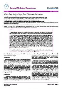
II. COMPARISON OF THREE DIFFERENT TYPES OF HIP DETECTORS The basic structure of HIP detectors consists of a heavily doped layer, which acts as the IR absorber region, and an intrinsic (or lightly doped) layer across which most of the external bias is dropped. According to- the doping concentration level in the heavily doped layer, the HIP detectors can be divided into three types as shown in Figs. l(a)-(c), which show different photoresponse mechanisms and response wavelength ranges. A. Type-l HIP detectors:
NdcNc (EF
e-
EF
-----lbias L n++
i (n-
or P-)
n-
FIG. 1. Energy band diagrams for three different types of HIP detectors. (a) Type I: Nd