Microshield is a partially shielded, planar transmission line in which the center ..... [1] G. M. Rebeiz, D. P. Kasilingarn, Y. Guo, P. A. Stimson and D. B. Rutledge, ...
Fourth International Symposium on Space Terahertz Technology
Page 223
FABRICATION AND CHARACTERIZATION OF MICROSHIELD CIRCUITS T. M. Weller, L. P. Katehi, and G. M. Rebeiz U of M NASA Center for Space Terahertz Technology H. J. Cheng and J. F. Whitaker Center for Ultrafast Optical Science Abstract Microshield is a partially shielded, planar transmission line in which the center conductor and upper ground planes are surrounded by air and supported by a 1.5 pm thick dielectric membrane. This configuration allows single-mode, TEM wave propagation over a broad bandwidth with very low dispersion and zero dielectric loss. A lower shielding cavity is used to minimize radiation loss, vary the characteristic impedance, and prevent power loss into substrate modes. These properties highlight the potential of microshield as a high performance medium for submillimeter wave transmission. Here we present an overview of the fabrication of microshield lines, and report on the recent progress in the characterization of various circuit structures. Theoretical and experimental results are shown for lowpass filters, transitions to grounded coplanar waveguide, and different resonant stub designs. A description of an ultrafast electro-optic sampling ex p eriment using membrane-based coplanar strip transmission lines is also included, and preliminary data is presented for line losses up to 500 GHz.
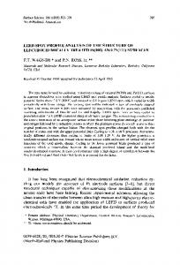
I Introduction In 1988 a subrnillimeter wave integrated-horn antenna was developed which contained a dipole suspended on a 1.5 pm thick dielectric membrane inside a silicon cavity [1]. The success of this technique has led to the application of the membrane technology to a variety of antenna geometries, including wideband millimeter wave power meters and corner cube arrays at 1.2 THz [2, 3]. The potential for low loss, non dispersive electromagnetic wave transmission eventually led to the introduction of the microshield transmission line in 1991 [4]. Mic °shield is a partially shielded, planar transmission line in which the center conductor and upper ground planes are surrounded by air and supported by the dielectric membrane. This configuration, which is shown in Figure 1, allows single mode TEM wave propagation over a broad
Page 224
Fourth International Symposium on Space Terahertz Technology
Upper Ground Planes
Silicon Wafer Lower Shielding Cavity Figure 1: Illustration of the microshield transmission line geometry. bandwidth with very low dispersion and zero dielectric loss. The lower shielding cavity is used to minimize radiation loss, vary the characteristic impedance, and prevent power loss into substrate modes. It also serves to equalize the upper ground planes, thereby eliminating the need for airbridges or via-holes. Based on the potential high-performance from this geometry, the microshield line is currently being investigated as an alternative for submillimeter wave-guiding applications. The characteristics of the microshield geometry were first examined in the theoretical study by Dib, et al [4, 5]. It was shown, for example, that discontinuities in microshield radiate less than comparable coplanar waveguide circuits, primarily due to the field confinement provided by the lower shielding cavity. Even on uniform transmission lines, frequency-dependent radiation into the substrate, which increases with the relative permittivity, can be significant at submillimeter wave frequencies. This loss mechanism is clearly minimized with microshield, since the conductors are completely surrounded by air. Finally, characteristic impedances ranging from around 30 S2 to over 280 ft can easily be obtained by varying the center conductor width, upper ground plane spacing, and the height and width of the shielding cavity. Accurate, closed-form expressions for the characteristic impedance have been derived using a conformal mapping approach [5]. Here we present an overview of the fabrication of microshield lines and report on the recent progress in the characterization of various circuit structures. Theoretical and experimental results
Fourth International Symposium on Space Terahertz Technology
Page 225
from 20-40 GHz are shown for lowpass filters, transitions to grounded coplanar waveguide (gcpw), and two resonant stub designs. The insertion loss of a 5-section filter was measured at < .3 dB at 25 GHz, and the response compared nearly identically with ideal transmission line theory predictions. A low-loss transition to gcpw was also fabricated which had an S 11 below -15 dB across the frequency range. The last section describes an ultra-fast optoelectronic sampling experiment using coplanar strip transmission lines printed on the dielectric membranes. Preliminary data on the loss characteristics up to 500 GHz demonstrates a definite advantage of membrane lines versus lines printed on high dielectric constant materials such as silicon or GaAs.
II Microshield Fabrication The fabrication of microshield begins with a silicon wafer which has membrane layers on both sides. The membrane is a composite Si0 2 /Si 3 N4 /Si0 2 material which is grown using a combination thermal oxidation/chemical vapor deposition process. The wafers used here are 340 pm thick, high-resistivity silicon wafers ilith a < 100 > orientation. The microshield structure is formed by first removing photolithographically defined regions from the membrane layer on the back side of the wafer. This pattern serves as an etch mask, allowing pyramidal cavities to be opened in the wafer using anisotropic Si etchants, such as ethylene diamme pyrocatechol (EDP) or potassium hydroxide (KOH). When the wafer has been etched through to the front side, the upper membrane layer will behave as an etch stop, thereby forming the exposed membrane surface with surrounding silicon walls below. The final step in the fabrication process is the metallization of the circuit pattern and the lower cavity sidewalls. A tri-layer photoresist/alummumiphotoresist technique with metal evaporation is used to deposit the circuit pattern on the top side of the membrane layer. Evaporation is also used for metal deposition from the backside onto the cavity sidewalls, but here some shadowing is required to protect selected areas of the membrane from metallization. A diced or micro-machined silicon mask is used to shield the region between the inner-edges of the upper ground planes and The pyramidal shape of the cavity is due to the varying rate at which the etchant attacks different surface orientations inside the silicon.
Fourth International Symposium on Space Terahertz Technology
Page 226
the center conductor, thus preventing metallization of the membrane below the slots. The finished circuits are then mounted on a gl:ound plane to fully enclose the lower shielding cavity.
III Theoretical Characterization A rigorous full-wave analysis is being developed for use in the theoretical characterization of microshield circuits. The formulation involves a space-domain integral equation (SDIE) that is generated through the application of equivalent currents. This approach has previously been applied in a variety of electromagnetic problems, such as the characterization of coplanar waveguide [6], rectangular waveguide junctions [7], and scattering from microstrip patches [8]. This method is also well-suited to the study of microshield transmission lines, as it provides a relatively simple means of studying the different types circuit geometries which are possible. These geometries include step changes in the height and width of the shielding cavity and abrupt changes in the dielectric material, in addition to discontinuities in the metallization patterns of the signal line and upper ground planes. The first step in the analysis is to simplify the circuit geometry by applying the equivalence principle. Here fictitious metal surfaces are introduced in the slots of the metallization which transform each region of a circuit into either a closed metallic cavity (inside) or a ground plane in free space (outside). Upon each side of these surfaces magnetic currents are imposed which act as equivalent sources. To determine the strength of these unknown currents the condition of continuous tangential electric and magnetic fields is enforced over each of the fictitious planes. Since Ai = E x ft, where ñ is the outward unit normal in each region, continuity of Eta , is strictly satisfied by setting
fi
lower =
gupper =ii i . The continuity of _tit a n is expressed in terms of the
following integral equation: x
7 [GestV,P)-F aint( F, 7-5 )] • /1 /.9 ( P)di =
(1)
where G est,int are the magnetic field dyadic Green's functions external and internal to the metallic cavities, respectively, and is is the current assumed with the ideal current source model, which
Fourth International Symposium on Space Terahertz Technology
Page 227
is used as the excitation. The solution to (1) is obtained by first dividing each surface into subsections, and then expanding the unknown magnetic currents using localized piecewise-sinusoidal basis functions. Equation (1) is then enforced in an average sense over each of the subsections, and is solved by using the method of moments (Galerkin's method) to generate a system of linear equations based on the mutual coupling, or admittance, between each of the currents. The solution of this system yields the complex coefficients of these basis functions, which is equivalent to finding the tangential electric field. This field is in the form of pure standing waves, such that standard transmission line theory may be then used to extract the scattering parameters of the circuit under analysis [61 The formulation summarized above is used for the characterization of circuits which have discontinuities in just the upper metal layers. By extending this approach, it will be possible to analyze circuits such as T-junctions, shunt stubs with conformal cavities, and transitions between microshield and other planar lines such as coplanar waveguid.e. This extension primarily involves the use of equivalent current sheets in multiple planes, which serves to separate cavity discontinuities into homogeneous regions. The work in this area is currently in progress.
IV Theoretical and Experimental Results In this section we present results on the performance of grounded coplanar waveguide (gcpw) to microshield transitions, stepped-impedance lowpass filters and different resonant stub designs. All measurements were made from 20-40 GHz, using an Alessi microwave probe station connected to an HP 8510B network analyzer. The system was calibrated using the TRL (thru-reflect-line) technique. For the theoretical data, ideal transmission line theory was used to characterize the lowpass filters and proved to be very accurate. The resonant stub designs were characterized using the full-wave analysis, and this section includes a study of the effect of shield-geometry variation on the stub performance. The formulation for characterization of the gcpw-microshield transitions is currently being developed, and thus only experimental data is presented.
Page 228
Fourth International Symposium on Space Terahertz Technology
IV.1 (Grounded) CPW to Microshield Transitions The primary motivation for investigating the gcpw-to-microshield transition lies in optimizing the design for circuit measurements. As mentioned, these measurements are made using a microwave probe station. Since the membranes cannot reliably withstand the force of repeated probe contact, the contact pads for must be formed in gcpw, which necessitates the use of transitions from the gcpw to the microshield line under test. In order to calibrate the system, these transitions need to be designed for low reflection. There were four microshield-gcpw-microshield transitions which were measured. The structures consist of a section of grounded cpw of length
Ag cPw i2
at 40 GHz, which is positioned in the center of
a microshield line. The design is illustrated in Figure 2. In all cases the microshield geometry has a center conductor width, s, of 350 pm and a slot width, w, of 35 pm. The characteristic impedance for this line is 75 Z. For the four different designs, s + 2w in the gcpw was also held constant at 420 and center conductor widths of 35, 70, 140, and 280 pm were tested. These geometries result in characteristic impedances of 88, 71, 54, and 36 12, respectively. The measured S for the transitions is given in Figure 3. The best performance, less than -15 dB from 20 to 40 GHz, is obtained with the 70 pm transition, which is the design with the closest impedance match. This transition also had a measured loss, (1— 1 ,5111 2 — 1S 21 1 2 ), below -15 dB across the entire band.
Iv-.2 Stepped-Impedance Lowpass Filters Stepped-impedance lowpass filters were investigated since they are relatively easy to design and could demonstrate the low loss, TEM characteristics of microshield. In order to obtain the i mpedance ratios required to implement the chosen designs, a center conductor width ratio of 33 : 1 was necessary. The conductor widths and the impedances are shown in the schematic diagram of the 5-section filter given in Figure 4. The measured performance for 5- and 7-section 0.5 dB ripple Chebyshev designs is shown in Figure 5. Also shown is the theoretical response obtained using ideal transmission line theory,
Page 229
Fourth International Symposium on Space Terahertz Technology
(UPPER GROUND PLANE) MICROSHIELD Ac CENTER CONDUCTOR
420 MICRONS
•
„t o
•"" GCPW
MICROSHIELD )00
(UPPER GROUND PLANE) Figure 2: Illustration of the microshield to grounded cpw (coplanar waveguide) transition. The center conductor width, S, the slot width, W, and the length of the gcpw, L, are all indicated. L A 2. is --2 at 40 GHz. The slots in the gcpw are shaded to indicate that the substrate dielectric changes from air in the microshield to silicon in the gcpw section.
70 MICRONS 140 MICRONS 280 MICRONS
25.
30.
35.
40.
FREQUENCY [Gfiz] Figure 3: Measured S H response of four different microshield to grounded cpw transitions. The rnicroshield center conductor width is 350 microns. Each plot corresponds to a different center conductor width for the gcpw. In all cases, 2s-f-w is 420 microns for both microshield and gcpw lines.
Fourth International Symposium on Space Terahertz Technology
Page 230
(EDGE OF LOWER SHIELDING CAVITY)
Figure 4: Diagram of the 5-section stepped-impedance lowpass filter (not to scale). Dimensions are given in pm and the different impedance sections are indicated. The shaded regions are the upper ground planes, which have been marked to indicate the positions of the lower shielding cavity sidewalls. The distance between the cavity sidewalls is 1800 /Am . with empirically-derived corrections for the effective line extension at impedance steps {9}. The agreement is quite good, and the differences near cutoff (shown in the insets) result from a peak in the measured loss which is not accounted for by the theory.
TV.3 Resonant Stubs In this section the performance of a microshield shorted resonant stub is presented. The design which was implemented consists of a stub which is formed in the center conductor, and is of length A
4
at the resonant frequency. This will be referred to as the in-line series shorted stub (ILS). A
comparison of the measured and calculated results is first shown, followed by an illustration of the effects of varying the shielding cavity dimensions. In addition, the characteristics of the 1LS stub are compared to those of a stub which is formed in the upper ground planes, which is referred to as the ground plane series stub (GPS). It is noted here that the measured ILS circuit had cavity dimensions of height, It, = 340 pm, and width, w e = 1800 pm, as measured at the top of the cavity. The measured and predicted performance of the 1LS stub is shown in Figure 6, where Ckt. A refers to the theoretical data. A schematic of the upper metallization pattern is also shown in the figure. The deep resonance at 28 GHz is shifted down in frequency relative to the ideal
Page 231
Fourth International Symposium on Space Terahertz Technology
5-SECTION
7-SECTION
-10.
-20. ,, v ittli . S_11 Measuredk vc.t 4iii 1 ix
-30.
S.)1 Theory --
_40. 1 20.
..
S ..... 21 Measured
Ipi r,v,v ' It if
.4i
4 Iii v
- - S__21 Theyry.
25.
30.
35.
40.
FREQUENCY [GHz] Figure 5: Measured and theoretical response of a 5- and a 7-section stepped-impedance microshield filter.
Page 232
Fourth International Symposium on Space Terahertz Technology
35 350
FREQUENCY [Gliz] Figure 6: Measured and calculated response of the in-line series shorted stub, where Ckt. A refers to the calculated data. In the diagram on the right (not to scale), Ls = 2500 and L t 120. All dimensions are in pm. response, since the physical stub length is
A
at 29.3 Gliz, when account is taken of the short
transverse slot lengths, L t . In Figure 7, the effects of a reduced cavity size and upper shielding are demonstrated. The Ckt. B results represent the predicted performance with a lower cavity of dimensions h, = 100 m and w, = 420 Am, which is the practical minimum cavity size for this circuit. Clearly, the cavity has only second order effects, which can be explained by the small slot width of only 35 pm. The Ckt. C results represent the predicted performance for the geometry of Ckt. A when shielded symmetrically above and below. In this case near-ideal stub performance is obtained, as the resonance has shifted to s' 29.5 GHz. As mentioned, a comparison has been made between the in-line series shorted stub and an alternative design called the ground plane series stub. The theoretical performance of each stub, using the symmetric shielding configuration, is shown in Figure 8. The upper metallization pattern for the GPS is also given in this figure, where the total stub length is 2370 ,um, corresponding to a resonant frequency of around 32 Gift. The GPS has a much narrower 3-dB bandwidth, roughly 14% versus 52% for the ILS, but will radiate much more strongly in an open environment.
Page 233
Fourth International Symposium on Space Terahertz Technology
-5. -10.
S 1 1 Ckt. A S12 Oct.
-15.
Si 1 Ckt. B
-20.
S12 Ckt. B Si 1 Ckt. C
-25.
S12 Ckt. C
-30. 20.
25.
30.
35.
40.
FREQUENCY Figure 7: Theoretical response of different in-line series shorted stub geometries. Ckt. A has lower shielding cavity dimensions of 1800 x 340 ym (width by height), the Ckt. B cavity is 420 x 100 pm, and Ckt. C has the same cavity dimensions as A but is symmetrically shielded on the top and bottom.
35 350
FREQUENCY [GITz} Figure 8: Theoretical response of the in-line series stub (ES) versus the ground plane series stub configuration (GPS). The circuits are symmetrically shielded and have the same cavity dimensions as Ckt. A in Figure 7. In the diagram on the right (not to scale), L i = 420 pm and L, = 1950 iim.
Page 234
Fourth International Symposium on Space Terahertz Technology
V Electro-optic Sampling Experiment Another interesting structure that has been fabricated on the micron-thick membranes is a simple coplanar strip transmission line (CPS). This structure, devised in order to push the limits of high-frequency, guided-wave transmission, should be capable of supporting millimeter- and submillimeter-wave electronic signals with very little induced distortion. This is due to the fact that the degree of phase velocity dispersion experienced in hybrid-mode propagation on planar transmission lines, as well as the amount of frequency-dependent radiation of energy into the substrate of such structures, increases with the permittivity of the substrate. Therefore, the electric field of a signal travelling on a uniform CPS on a membrane substrate experiences essentially a homogeneous dielectric above and below the plane of the membrane, i.e. air. This leads to propagation that has no radiation loss, no substrate dielectric loss, and no dispersion due to a frequency-dependent effective permittivity. In this preliminary investigation, we have demonstrated that pulses having subpicosecond rise times and single-picosecond durations propagate for lengths as great as 5 mm without loss of fidelity. The usable frequency content of these pulses extends from dc to nearly 1 Tliz, and by taking Fourier transforms, we have computed the attenuation and phase velocity of the time-domain signals on the line. Between 50 and 500 GI-Iz, it has been observed that dispersion is negligible and attenuation
18 very
small, arising presumably only from ohmic losses in
the metal conductors. In order to generate and measure electrical pulses of such short duration and high frequency content, the optoelectronic technique of photoconductive switching, along with an ultra-high-speed electro-optic sampling characterization system, have been employed. These techniques are both based on the use of laser pulses of extremely short duration (< 100 Is). The photoconductive source requires the ultra-short laser pulse to convert a dc bias to a subpicosecond electrical transient, while electro-optic sampling uses the optical pulse with an electro-optic crystal to produce a sampling gate having a duration of only several tenths of a picosecond. A probe tip fashioned from the electro-optic crystal is dipped into the electric field above the transmission line under test, and without any electrical contact the propagating waveform is measured. For the measurement of transients in the time domain, reflections from any source near the probing
Fourth International Symposium on Space Terahertz Technology
Page 235
point cause a loss of accuracy in the acquisition of clean, easily analyzed signals. Therefore, it was necessary to integrate a 200-Am-wide photoconductive-generator patch with the CPS fabricated on the membrane. This was a convenient alternative compared with transporting a short electrical transient onto the CPS via inductive wirebonds or through the use of an unwieldy flip-chip geometry. The photoconductor of choice, having subpicosecond carrier lifetime, high dark resistivity, high responsivity, and high dielectric breakdown, was a 1-4/111 layer of GaAs grown by molecular beam epitaxy at the low substrate temperature of 200 deg C (LT-GaAs). This photoconductor was lifted off its substrate to form a free-standing film through etching techniques, and then grafted to the membrane substrate using a van der Waals bonding technique. The CPS was then defined on the LT-GaAs and the membrane using standard photolithographic techniques. The pulse output after optical excitation of the photoswitch was measured at distances of 1, 3, and 5 mm from the generator, with no discernable distortion except for a small decrease in peak amplitude at the 5 mm propagation distance. The measured pulse rise time was < 0.75 ps, and the FWITM (full width at half maximum) was < 1.2 ps. When the Fourier transforms of the time-domain signals were compared, the phase velocity between 50 and 500 GHz was found to be flat indicating the absence of dispersion. The attenuation, shown in Figure 9, was found to increase only slightly, to about 0.8 dB/mm at 500 GHz. This result can be directly compared to the propagation of a subpicosecond pulse along a CPS of the same dimensions on a GaAs substrate. While the attenuation at 50 GHz is only about 0.7 dB/mm for this structure, at 500 GHz it is in excess of 9.5 dB/mm. This is mainly due to the extreme radiation loss present even in uniform lines that are fabricated on high-permittivity substrates. A much larger degree of phase-velocity dispersion also results from propagation on the GaAs-substrate tine, leading to pulses with rise times and durations that rapidly expand with increasing propagation distance.
VI Conclusion This paper has presented a review of the recent progress made in the experimental and theoretical characterization of microshield transmission line circuits. Low loss transitions from microshield to grounded coplanar waveguide have been successfully designed and measured, and
Fourth International Symposium on Space Terahertz Technology
Page 236 10.00
-
GaAs substrate
1.00
membrane substrate
w=s=20 0.10
1
1
1
1
1
1
1
1
50 100 150 200 250 300 350 400 450 500 frequency (GHz)
Figure 9: Measured attenuation of a coplanar stripline (CPS) printed on a GaAs substrate compared to a line printed on a dielectric membrane. The measurements were made using an electro-optic sampling technique. The conductor and slot widths of the CPS are both 20 pm.
stepped-impedance lowpass filters demonstrated very good performance and compared quite well to ideal transmission line theory. A brief study of different microshield resonant stub designs has also been presented. Finally, a preliminary study using an ultra-fast electro-optic sampling technique has shown that coplanar strip lines, printed on the dielectric membranes, show strong potential as a low loss transmission medium for THz-frequency applications.
VII Acknowledgements This work has been supported by the Office of Naval Research under contract No. N0001492-J-1070, the NASA Center for Space Terahertz Technology, and the NSF under the Center for Ultrafast Optical Science. The authors would like to thank Prof. G. Rebeiz's group for their assistance, and particularly Mr. Walid Ali-Ahmad.
Fourth International Symposium on Space Terahertz Technology
Page 237
References [1] G. M. Rebeiz, D. P. Kasilingarn, Y. Guo, P. A. Stimson and D. B. Rutledge, "Monolithic MillimeterWave Two-Dimensional Horn Imaging Arrays", IEEE Trans. on Antennas and Propagation, Vol. 38, pp. 1473-1482, Sept. 1990. [2] Curtis C. Ling and Gabriel M. Rebeiz, "A Wide-Band Monolithic Quasi-Optical Power Meter for Millimeter- and Submillimeter-Wave Applications ", IEEE Trans. on Antennas and Propagation, Vol. 39, pp. 1257-1261, Aug. 1991. [3] Steven S. Gearhart, Curtis C. Ling, Gabriel M. Rebeiz, Hernant Davee, and Gordon Chin "Integrated 119-pm Linear Corner-Cube Array ", IEEE Microwave and Guided Wave Letters, Vol. 1, pp. 155-157, July 1991. [4] N. Dib, W. Harokopus, P. Katehi, C. Ling, and G. Rebeiz, "Study of a Novel Planar Transmission Line," 1991 IEEE MTT . S International Microwave Symposium Digest Boston, pp. 623-626. [5] N. I. Dib, P. B. Katehi, "Impedance Calculation for the Microshield Line," Microwave and Guided Letters, Vol. 2, No. 10, Oct. 1992, pp. 406-408. [6] N. I. Dib and P. B. Katehi, "Modeling of Shielded CPW Discontinuities Using the Space Domain Integral Equation Method (SDIE)," Journal of Electromagnetic Waves and Appiications,April 1991. [7] Z. Shen and R. Hua, "Moment method analysis of rectangular waveguide T-junctions having arbitrary cross-sections", Int. J. Electronics, 1991, Vol. 71, No. 3, 463-469. [8] K. Barkeshli and J. Volakis, "Electromagnetic Scattering from an Aperture Formed by a Rectangular Cavity Recessed in a Ground Plane , " Journal of Electromagnetic Waves and Applications, Vol. 5, No. 7, pp. 715-734, 1991. [9] E. 0. Hammerstad and F. Bekkadal, A Microstrip Handbook ELAB Report, STF 44 A74169, N7034, University of Trondheim, Norway, 1975.