APPLIED PHYSICS LETTERS 96, 112904 共2010兲
Identification of the controlling parameter for the set-state resistance of a TiO2 resistive switching cell Seul Ji Song,1 Kyung Min Kim,1 Gun Hwan Kim,1 Min Hwan Lee,1 Jun Yeong Seok,1 Ranju Jung,2,a兲 and Cheol Seong Hwang1,b兲 1
Department of Materials Science and Engineering and Inter-university Semiconductor Research Center, Seoul National University, Seoul 151-744, Republic of Korea 2 Department of Electrophysics, Kwangwoon University, Seoul 139-701, Republic of Korea
共Received 15 June 2009; accepted 14 February 2010; published online 18 March 2010兲 This study examined the parameter controlling the set-state resistance 共Rset兲 of a Pt/ TiO2 / Pt resistive switching 共RS兲 cell in unipolar RS mode. Although the compliance current in the current-voltage sweep had some effect on the Rset, the uncontrolled flow of charge from the parametric analyzer prevented making an accurate estimation of the parameters. The current transient in pulse switching observed using a high-speed digital oscilloscope and physical modeling showed that the capacitive charge moves vigorously at the moment of on-switching, and Rset is governed by the level of migrating charge. The actual switching time was Ⰶ50 ns. © 2010 American Institute of Physics. 关doi:10.1063/1.3355415兴 Recently, resistance switching 共RS兲 phenomena have been studied actively in a variety of thin film materials in order to apply them to the next generation of nonvolatile memory.1–3 The unipolar RS process is performed by applying the same bias polarity, and has been understood from the formation 关set, switching from a high resistance state 共HRS兲 to a low resistance state 共LRS兲兴 and rupture 共reset, switching from the LRS to HRS兲 of conducting filaments 共CFs兲 in several oxides. n-type conducting TiO2 was reported to show typical unipolar RS behavior.4–7 CF growth was initiated by carrier 共electron兲 injection from the cathode interface, and the thermal-energy assisted 共Joule heating兲 field-driven migration of oxygen vacancies. The formation/rupture of the conical shaped metallic Magnéli phase CF caused RS in TiO2.8–10 One of the problems with RS is the nonuniform switching parameters, such as the set and reset voltages 共Vset and Vreset兲 and resistances 共Rset and Rreset兲. This might be closely related to the nonuniform generation and rupture of the CF. Therefore, it is essential to examine the controlling parameter that governs the formation and rupture of CF to improve the performance of RS.11–13 In this study, the current flow at the moment of set switching with either the current–voltage 共I–V兲 sweep or pulse switching modes was monitored carefully, and its correlation with the Rset was examined. The preparation of a Pt/60-nm-thick TiO2 / Pt film and method for RS of the sample is reported in detail elsewhere.8,9,11 RS was examined using a semiconductor parameter analyzer 共SPA, HP 4145B兲 in voltage sweep mode with the proper compliance currents 共Icomp兲. The transient current at the moment of set switching after reaching the Icomp was monitored using a digital oscilloscope 共OSC, Tektronix 684C兲 employing the circuit schematics shown in the inset in Fig. 1共a兲. The input impedance of SPA was much lower 共⬃ ⬍ 1 ⍀兲 than that of the OSC. Therefore, a R⬘ value of 17 ⍀ was adopted. Pulse switching with a constant volta兲
Electronic mail:
[email protected]. Electronic mail:
[email protected].
b兲
0003-6951/2010/96共11兲/112904/3/$30.00
age supply was performed using an HP81110A pulse generator 共PG兲 and the same OSC, as shown in the inset of Fig. 2共b兲. The transient current through the OSC was monitored by dividing the measured voltage with the internal resistance of the OSC 共ROSC, 50 ⍀兲. A constant current pulse 共80 mA兲 was programmed to the PG. Since the PG has an internal resistance of 50 ⍀ in parallel with the load resistance, the measured current by the OSC was determined by the relative resistance ratio of the internal resistance of PG and load resistance. Here, the load resistance is the sum of the sample resistance and ROSC. When set switching occurs, the sample resistance decreases and the current through the sample-OSC path increases. The parasitic capacitance of PG 共CPG兲, contact resistance 共RC兲, and circuit parasitic capacitance 共Cpara兲 when contact probes were installed were estimated using the estimated the time constant 共兲 of the circuit from the decaying edge of a current pulse monitored by the OSC of the circuit set-ups described below. The PG was connected directly to the OSC by a cable with a configuration corresponding to a parallel circuit of CPG and RPG 共50 ⍀兲. The estimated from the current pulse input was 2.14 ns, suggesting that CPG = 85 pF 共total resistance= 25 ⍀, so 2.14 ns= 85 pF⫻ 25 ⍀兲. The same procedure was then performed with the cable being replaced with the contact probes containing RC and Cpara. The dc type measurements revealed a RC value of ⬃2 ⍀. In this case, the equivalent circuit must correspond to a parallel combination of CPG, RPG, Cpara, and
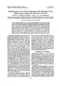
FIG. 1. 共Color online兲 共a兲 Time evolution of current with various Icomp values near the moment when set switching occurs during the I–V sweeps, 共b兲 change in Rset as a function of Icomp, and 共c兲 relationship between the Rset and peak OSC current with various Icomp values.
96, 112904-1
© 2010 American Institute of Physics
112904-2
Song et al.
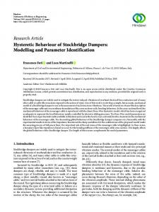
FIG. 2. 共Color online兲 共a兲 Typical time evolution curves of current when set switching occurred 共closed circle symbol兲 and did not occur 共open triangle symbol兲 by applying a pulse with a 300 ns duration and 80 mA amplitude to the sample. 共Blue兲 solid line shows the numerically fitted results and 共red兲 dashed line shows the simulated curve considering the dc leakage and noise component. The extracted Gaussian functions for the Qs and Qd estimation are represented by green lines. 共b兲 Variation in the Rset as a function of Qs for capacitors with various areas. The inset shows a circuit diagram for the pulse switching measurements.
RC + ROSC 共52 ⍀兲. The estimated from the current pulse input was 6.10 ns, suggesting that Cpara = 190 pF. The parasitic capacitance of the SPA was determined to be ⬃50 nF when a set state sample 共R ⬃ 30 ⍀兲 was connected 共 ⬃ 2 s, and total R ⬃ 40 ⍀兲. Figure 1共a兲 shows the time evolution of the current by the OSC near the moment when set switching occurs during the I–V sweeps with various Icomp values. The sample was initially under the HRS state and Vset was determined previously using an I–V sweep. The total current that passed through the sample can also be calculated easily using the circuit diagram and OSC current shown in Fig. 1共a兲. Generally, the peak current increases with increasing Icomp. When the detected peak current reached Icomp, the SPA supplied a constant voltage that maintained the Icomp. The monitored current then decreased to a certain saturated value after a certain transient time. The saturation current level increased with increasing Icomp after a much longer time than that shown in Fig. 1共a兲 due to the very long measurement time of SPA 共tens of milliseconds兲. The long decay time of the current after the peak current was due to the large parasitic capacitance 共⬃50 nF兲 of SPA. After each set switching, the Rset was calculated using the current value at 0.2 V considering the R⬘ and OSC resistance. Figure 1共b兲 shows the measured Rset as a function of Icomp. Rset decreased with increasing Icomp, which is in agreement with a previous report.7 Figure 1共c兲 shows the relationship between the Rset and peak OSC current with various Icomp values. Although a vague inverse relationship can be found between them, the data variance is severe, even for a given Icomp, which makes it difficult to identify the parameter determining set switching. The total charge migration after reaching the peak current can be calculated by integrating the current with respect to time. The total charge also showed a similarly scattered correlation with Rset 共data not shown兲. This is due primarily to the uncontrolled decay of the current supplied from the SPA after reaching the Icomp. As shown in Fig. 1共a兲, the decay takes usually 1 – 2 s, but actual set-switching occurs for only a few tens of nanoseconds, as will be shown later. Therefore, the current after reaching the peak current modified the CF in a relatively uncontrolled manner. In addition, there was a sharp peak at time ⬃0 s, which corresponds to
Appl. Phys. Lett. 96, 112904 共2010兲
the dissipation of the capacitive charge 共of the HRS sample兲 at the moment of set switching. As shown in Fig. 2, this dissipation of capacitive charge is the actual controlling parameter for Rset. Compared to this relatively tiny charge flow, a much larger 共uncontrolled兲 current flowed after setswitching had occurred for the following few microseconds. This affects the state of the CF significantly, and the resulting Rset is not well controlled. While previous studies14,15 reported that the parasitic capacitance usually causes a decrease in Rset, the present work showed that this is not necessarily the case, as can be verified from Fig. 1共c兲. As discussed below, this is due to the dissipation of the charge that accumulated on the RS cell itself during set switching. Figure 2共a兲 shows typical curves of time evolution of current when set switching occurred 共filled circle symbol兲 and when it did not occur 共open triangle symbol兲 after supplying a square shaped current pulse with a 300 ns duration. The sample was initially under the HRS state by applying the proper I–V sweeps. In the case where set switching occurred, three major features were observed in the curve. First, there are two current levels 共⬃15 mA between ⬃0 and 150 ns and ⬃30 mA after ⬃200 ns兲. This must correspond to the dc leakage current for the HRS and LRS, respectively. The estimated reset state resistance from the I–V curves immediately before set switching occurred varied from ⬃150 to 1000 ⍀, while it was ⬃104 ⍀ at 0.2 V due to the nonlinear nature of the reset state sample. The set state resistance was typically ⬃30 ⍀. The expected current though the OSC was 16 and 31 mA when the reset and set resistances were 200 and 30 ⍀, respectively, during pulse switching. This coincides well with the data shown in Fig. 2共a兲. Second, there were two initial peaks at the beginning of the pulse application. The first peak corresponds to the instantaneous dc leakage response through Rreset with a rising time of ⬃2 ns 共which is the specified rising time of PG兲. The second peak 共at time ⬃20 ns兲 corresponds to capacitive charging of the HRS sample. The time delay 共⬃10 ns兲 was attributed to the parasitic circuit capacitance. Therefore, the HRS sample can be represented by a parallel combination of a capacitance and Rreset.16 The third feature is the distortion of the curves due to the circuit noise and ringing of the PG 共5% overshoot from the specification兲.17 Indeed, this noise component of the whole circuit, including the inductance component of PG, modifies the capacitive charging peak shape from the standard exponential form 共⬃e−t/, where ⬃ RC兲 into a Gaussian-type form 共green line兲.17 Therefore, the current transient with time was simulated considering the noise component and dc leakage current, as represented by the 共red兲 dashed line in Fig. 2共a兲. The difference between the measured 共closed circle symbol兲 and simulated curves corresponds to the capacitive charge/dissipation current components. Interestingly, two of the capacitive components were extracted from this procedure. The first peaked at ⬃20 ns and the second peaked at ⬃200 ns. The first and second components must be due to charging of the capacitor and the dissipation 共leakage兲 of stored charge through the CF 共which has been formed immediately after set switching兲, respectively. The rising slope at ⬃200 ns becomes smaller than the falling slope when the pulse was terminated due to the involvement of this charged current dissipation. The stored and dissipated charges can be estimated by the integration of cur-
112904-3
Appl. Phys. Lett. 96, 112904 共2010兲
Song et al.
rent with time. Figure 2共a兲 shows that the stored 共Qs兲 and dissipated 共Qd兲 charges were 199.7 and 210.7 pC, respectively, for this specific case. The capacitance–voltage 共C–V兲 curve of the HRS sample was estimated using an impedance analyzer 共HP 4194A兲. Due to the presence of a parallel Rreset, a large dc leakage current was involved in the C–V measurement, which did not allow an accurate estimation of the C value in the V region from 1 to 2 V. However, the C value extracted from the C–V measurement was ⬃100 pF, suggesting that the accumulated charge was ⬃200 pC when a dc pulse of 2 V 共corresponding to the programmed current兲 was applied. The contribution of the parasitic charge to charge flow at the moment of set switching was ⬃6% of the total charge. The case when set switching did not occur, even with the same pulse, can be explained by the fact that 2 V is close to the threshold value for set switching in pulse switching mode. In this case, the HRS sample works as a normal leaky capacitor. Hence, the initial capacitive charge flows in the opposite direction at the end of the voltage pulse. When set switching occurs, this discharging with an opposite current flow 共at 300 ns兲 does not appear because the stored charge has leaked away through the CF. Figure 2共b兲 shows the change in Rset as a function of Qs for capacitors with various areas. The Qs values ranged from ⬃70 to 250 pC, which are reasonable considering the C–V results. Rset showed an inverse relationship with Qs all over capacitor areas. A similar relationship holds between the Rset and Qd, as Qs ⬃ Qd. Other parameters, such as the peak current and total charge flow during the entire pulse RS procedure, did not show such a clear correlation with Rset. Therefore, the discharging of the capacitive charge at the moment of set switching appears to be the key parameter in determining Rset. During the period of pulse application before actual set switching occurs, the electromigration of oxygen vacancies and their possible rearrangement to form an embryonic CF may have occurred. When this conducting path is formed, the stored Qs begins to flow suddenly through this tiny CF, which makes the CF stronger and the resulting Rset lower. The random variation in Qs 共and Qd兲 shown in Fig. 2共b兲 is due to the somewhat random charging of the capacitor during the previous reset process. The relatively randomized geometric/electric status of the ruptured CF might have caused the random charging of the HRS sample. When the pulse duration becomes excessively long 共⬎microseconds兲, the dc leakage after set switching may overwhelm the Qs effect in determining the Rset. However, this type of operation is unlikely in the actual operation of an RS device; better speed and repeatability can be expected if the period is shorter after the set RS occurs. Indeed, if the pulse duration is too long, the sample sometimes returns to the HRS again due to the excessive current flow. Finally, the actual CF formation time before stabilization must correspond to the time needed to dissipate the Qs 共⬃50 ns in this experiment兲. However, it is believed that
such a large amount of charge flow may not be necessary to stabilize the tiny CF in a small RS cell 共Ⰶ100⫻ 100 nm2兲. In summary, this study examined the correlation between the set-state resistance and current 共charge兲 flow during set switching in both the I–V sweep and pulse switching experiments. The relatively uncontrolled decay of the SPA output current after reaching the Icomp in the I–V sweep made the RS less uniform. This was due to the involvement of large parasitic charge from the circuit. For a more practical pulse switching case, the dissipation of stored capacitive charge through the formed CF dominantly controlled the Rset. This suggests that the memory cell size might have a crucial influence on the reliability of RS in TiO2. The authors acknowledge the support of the National Research Program for the Nano Semiconductor Apparatus Development sponsored by the Korea Ministry of Knowledge and Economy, the National Program for 0.1Terabit NVM Devices, Korea Research Foundation grant 共MOEHRD, Basic Research Promotion Fund, KRF-2008-C00029兲, a National Research Foundation of Korea 共2009-0081961兲, and World Class University program 共R31-2008-00010075-0兲 through the Korea Science and Engineering Foundation funded by the Ministry of Education, Science, and Technology. 1
A. Beck, J. G. Bednorz, C. Gerber, C. Rossel, and D. Widmer, Appl. Phys. Lett. 77, 139 共2000兲. 2 A. Sawa, Mater. Today 11, 28 共2008兲. 3 D. B. Strukov, G. S. Snider, D. R. Stewart, and R. S. Williams, Nature 共London兲 453, 80 共2008兲. 4 K. Szot, W. Speier, G. Bihlmayer, and R. Waser, Nature Mater. 5, 312 共2006兲. 5 D. C. Kim, S. Seo, S. E. Ahn, D.-S. Suh, M. J. Lee, B.-H. Park, I. K. Yoo, I. G. Baek, H.-J. Kim, E. K. Yim, J. E. Lee, S. O. Park, H. S. Kim, U.-I. Chung, J. T. Moon, and B. I. Ryu, Appl. Phys. Lett. 88, 202102 共2006兲. 6 B. J. Choi, D. S. Jeong, S. K. Kim, S. Choi, J. H. Oh, C. Rohde, H. J. Kim, C. S. Hwang, K. Szot, R. Waser, B. Reichenberg, and S. Tiedke, J. Appl. Phys. 98, 033715 共2005兲. 7 C. Rohde, B. J. Choi, D. S. Jeong, S. Choi, J.-S. Zhao, and C. S. Hwang, Appl. Phys. Lett. 86, 262907 共2005兲. 8 K. M. Kim, B. J. Choi, Y. C. Shin, S. Choi, and C. S. Hwang, Appl. Phys. Lett. 91, 012907 共2007兲. 9 K. M. Kim, B. J. Choi, B. W. Koo, S. Choi, D. S. Jeong, and C. S. Hwang, Electrochem. Solid-State Lett. 9, G343 共2006兲. 10 D.-H. Kwon, K. M. Kim, J. H. Jang, J. M. Jeon, M. H. Lee, G. H. Kim, X.-S. Li, G.-S. Park, B. Lee, S. Han, M. Kim, and C. S. Hwang, Nature Nanotechnol. 5, 148 共2010兲. 11 K. M. Kim and C. S. Hwang, Appl. Phys. Lett. 94, 122109 共2009兲. 12 D. C. Kim, M. J. Lee, S. E. Ahn, S. Seo, J. C. Park, I. K. Yoo, I. G. Baek, H. J. Kim, E. K. Yim, J. E. Lee, S. O. Park, H. S. Kim, U.-I. Chung, J. T. Moon, and B. I. Ryu, Appl. Phys. Lett. 88, 232106 共2006兲. 13 R. Jung, M.-J. Lee, S. Seo, D. C. Kim, G.-S. Park, K. Kim, S. Ahn, Y. Park, I.-K. Yoo, J.-S. Kim, and B. H. Park, Appl. Phys. Lett. 91, 022112 共2007兲. 14 K. Kinoshita, K. Tsunoda, Y. Sato, H. Noshiro, S. Yagaki, M. Aoki, and Y. Sugiyama, Appl. Phys. Lett. 93, 033506 共2008兲. 15 D. Ielmini, C. Cagli, and F. Nardi, Appl. Phys. Lett. 94, 063511 共2009兲. 16 D. S. Jeong, H. Schroeder, and R. Waser, Appl. Phys. Lett. 89, 082909 共2006兲. 17 A. R. Hambley, Electrical Engineering: Principles and Applications, 3rd ed. 共Prentice Hall, New Jersey, 2004兲, pp. 167–179.