To Appear in the Sixth International Symposium on High-Performance Computer Architecture (HPCA), January 2000.
Impact of Chip-Level Integration on Performance of OLTP Workloads Luiz Andr´e Barroso, Kourosh Gharachorloo, Andreas Nowatzyk and Ben Verghese Western Research Laboratory Compaq Computer Corporation fbarroso,kourosh,
[email protected],
[email protected]
Abstract With increasing chip densities, future microprocessor designs have the opportunity to integrate many of the traditional systemlevel modules onto the same chip as the processor. Some current designs already integrate extremely large on-chip caches, and there are aggressive next-generation designs that attempt to also integrate the memory controller, coherence hardware, and network router all onto a single chip. The tight coupling of these modules will enable efficient memory systems with substantially better latency and bandwidth characteristics relative to current designs. Among the important application areas for high-performance servers, online transaction processing (OLTP) workloads are likely to benefit most from these trends due to their large instruction and data footprints and high communication miss rates. This paper examines the design trade-offs that arise as more system functionality is integrated onto the processor chip, and identifies a number of important architectural choices that are influenced by chip-level integration. In addition, the paper presents a detailed study of the performance impact of chip-level integration in the context of OLTP workloads. Our results are based on full system simulations of the Oracle commercial database engine running on both in-order and out-of-order issue processors used in uniprocessor and multiprocessor configurations. The results show that chip-level integration can improve the performance of both configurations by about 1.4 to 1.5 times, though for different reasons. For uniprocessors, integration of the L2 cache and the resulting lower hit latency is the primary factor in performance improvement. For multiprocessors, the improvement comes from both the integration of the L2 cache (lower L2 hit latency) and the integration of the other memory system components (better dirty remote latency). Furthermore, we find that the higher associativity afforded by integrating the L2 cache plays a critical role in counteracting the loss of capacity relative to larger off-chip caches. Finally, we find that the relative gains from chip-level integration are virtually identical for in-order and out-of-order processors.
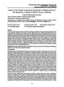
1 Introduction Advances in semiconductor technology enable next-generation microprocessor designs with well over a hundred million tran-
sistors on a single die. At the same time, the increasing density and speed of transistors make off-chip communication relatively more expensive. These technology trends provide an incentive to integrate functional modules that traditionally appear at the system-level onto the same die as the processor. The current HP PA-8500 microprocessor already integrates a 1MB data cache and a 0.5MB instruction cache with the processor. Similarly, the next-generation Alpha 21364 plans to aggressively exploit such integration by including a 1GHz 21264 core, two levels of caches, memory controller, coherence hardware, and network router all on a single die. Figure 1 shows a block diagram of the Alpha 21364 along with how the processors can be connected to form a scalable multiprocessor. The primary benefits from integrating modules onto a single chip arise from more efficient communication interfaces. First, there are fewer signals that cross chip boundaries, leading to lower latency communication. Second, integration allows for substantially higher communication bandwidths by removing constraints imposed by scarce external pin resources. Finally, the tight coupling may in some cases enable novel interactions among modules that would not be feasible across chip boundaries. In the context of high-performance processors, these benefits typically translate into a lower latency and higher bandwidth cache hierarchy and memory system. Chip-level integration provides other advantages besides higher performance. A key benefit is lower system component counts which leads to more reliable and lower cost systems that are easier to manufacture and maintain. Compute power density (e.g., computes per cubic foot) is also clearly improved through integration. Another possible benefit of integration is reduced design complexity that arises from eliminating generalized transactional interfaces that are typically used when modules communicate across chip boundaries.1 Finally, designs that provide on-chip cache-coherence support, such as the Alpha 21364, lead to faster turnaround times for incorporating the latest microprocessors in multiprocessor servers. Given that commercial applications such as databases and Web servers constitute the largest and fastest-growing segment of the market for high-performance servers, it is important to evaluate the impact of chip-level integration in the context of 1 However, eliminating such interfaces must be done with care to keep verification costs in check; tightly integrated units that lack well structured and observable interfaces must be tested as a single entity and are harder to verify.
CPU I-Cache
L2-Cache Controller
L2-Cache on-chip SRAM
D-Cache
Memory Controller
Coherency Controller & Network Interface
L2 Victim Buffers
Router
Off-chip DRAM Array
I/O
Other Nodes
A: Single Node Memory
364
Memory
364
Memory
364
I/O
I/O
I/O
Memory
Memory
Memory
364
364
364
I/O
I/O
I/O
Memory
Memory
Memory
364
364
364
I/O
I/O
I/O
Memory
Memory
Memory
364
364 I/O
364 I/O
I/O
B: MP-System
Figure 1: Block diagram of the Alpha 21364. these workloads. While applications such as decision support (DSS) and Web index search have been shown to be relatively insensitive to memory system performance [1], a number of recent studies have underscored the radically different behavior of online transaction processing (OLTP) workloads [1, 2, 3, 8, 12, 15, 18]. In general, OLTP workloads lead to inefficient executions with a large memory stall component and present a more challenging set of requirements for processor and memory system design. This behavior arises from large instruction and data footprints and high communication miss rates that are characteristic for such workloads [1]. At the same time, the increasing popularity of electronic commerce on the Web further elevates the importance of achieving good performance on OLTP workloads. This paper explores the general design trade-offs that arise as more system-level modules are incorporated onto the processor chip, and presents a detailed study of the impact of chip-level integration on the performance of OLTP workloads. We consider successively integrating (i) the second-level cache, (ii) memory controllers, and (iii) coherence hardware and network router. In each case, we identify important architectural trade-offs that are influenced by the integration and analyze their performance impact for both uniprocessor and multiprocessor configurations, and in-order and out-of-order processor models. Since previ-
ous results on OLTP show the need for extremely large off-chip caches [1, 8], we also consider the viability of larger off-chip caches in a fully integrated design. Our performance results for OLTP are based on full system simulations, including operating system activity, of the Oracle commercial database engine (version 7.3.2) running under Compaq Tru64 Unix (previously known as Digital Unix). Our simulation parameters are based on an aggressive 0.18um CMOS technology that will be used in next-generation microprocessors such as the Alpha 21364. Our results show that chip-level integration of the memory system can yield about a 1.4 times improvement in OLTP performance over an aggressive non-integrated design, for both uniprocessor and multiprocessor configurations. Relative to less aggressive off-chip multiprocessor designs, these gains can be as high as 1.5 to 1.6 times. We find that uniprocessor OLTP performance is primarily determined by the size, organization and latency of the L2 cache and is relatively insensitive to the rest of the memory system. Therefore, the primary performance benefit comes from integrating the L2 cache with the processor. Multiprocessor OLTP performance is also dependent on the latency of dirty remote (3-hop) misses. Therefore, the performance benefits in multiprocessor configurations come from both integrating the L2 (lower L2 hit latency) and from integrating the other system components (lower dirty miss latency). We also observe that there is synergy in tightly coupling the coherence and memory controllers, and separating these two system components can lead to sub-optimal designs. Finally, our analysis shows that there is little justification for augmenting a fully integrated design with larger off-chip caches. One of the most interesting results of this paper is with respect to the effectiveness of smaller on-chip L2 caches in capturing the footprint of OLTP workloads. Previous studies of OLTP have pointed to the need for large off-chip caches. Surprisingly, we find that the limited capacity of an on-chip L2 cache is more than offset by the higher associativity that is made viable by the integration. In fact, a 2MB on-chip cache with 4-way or 8-way associativity exhibits fewer misses than an 8MB direct-mapped off-chip cache. This extreme sensitivity of OLTP workloads to associativity shows that many of the misses eliminated by large direct-mapped off-chip caches are actually conflict misses as opposed to true capacity misses. The rest of paper is structured as follows. The next section presents our experimental methodology, including a brief description of the OLTP workload and the simulated architectures. Sections 3, 4, and 5 evaluate the trade-offs of successively integrating the second-level cache, memory controller, and coherence controller and network router onto the processor chip. We evaluate the viability of large off-chip third-level caches for integrated designs in Section 6. Section 7 shows that the relative benefits of on-chip integration are virtually identical for in-order and out-of-order processors. Finally, we discuss related work and conclude.
2 Methodology This section describes the OLTP workload, simulation platform, and memory system parameters that are used in this study.
affect both benchmarks in similar ways. Finally, it is widely acknowledged that actual customer database applications typically exhibit poorer performance than TPC-C itself.
2.2 2.1 OLTP Workload Online transaction processing systems are used in day-to-day business operations (e.g., airline reservations), and are characterized by a large number of clients who continually access and update small portions of the database through short running transactions. Our OLTP workload is modeled after the TPC-B benchmark [20]. This benchmark models a banking database system that keeps track of customers' account balances, as well as balances per branch and teller. Each transaction updates a randomly chosen account balance, which includes updating the balance of the branch the customer belongs to and the teller from which the transaction is submitted. It also adds an entry to the history table which keeps a record of all submitted transactions. We use the Oracle 7.3.2 commercial database management system as our database engine. In addition to the server processes that execute the actual database transactions, Oracle spawns a few daemon processes that perform a variety of duties in the execution of the database engine. Two of these daemons, the database writer and the log writer, participate directly in the execution of transactions. The database writer daemon periodically flushes modified database blocks that are cached in memory out to disk. The log writer daemon is responsible for writing transaction logs to disk before it allows a server to commit a transaction. Client processes communicate with server processes through pipes, and the various Oracle processes (i.e., daemons and servers) communicate through a shared memory region called the System Global Area (SGA). The SGA consists of two main regions - the block buffer area and the metadata area. The block buffer area is used as a memory cache of database disk blocks. The metadata area is used to keep directory information for the block buffer, as well as for communication and synchronization between the various Oracle processes. Our OLTP workload is set up and scaled in a similar way to a previous study which validated such scaling [1]. We use a TPCB database with 40 branches with an SGA size of over 900MB (the size of the metadata area is over 100MB). Our runs consist of 2000 transactions after a warmup period. We use Oracle in a dedicated mode for this workload, whereby each client process has a dedicated server process for serving its transactions. To hide I/O latencies, including the latency of log writes, OLTP runs are usually configured with multiple server processes per processor. We use 8 processes per processor in this study. We chose to use TPC-B instead of TPC-C (the current official transaction processing benchmark from TPC) for a variety of reasons. First, TPC-B has much simpler setup requirements than TPC-C, and therefore lends itself better for experimentation through simulation. Second, our performance monitoring experiments with TPC-B and TPC-C show similar processor and memory system behavior, with TPC-B exhibiting somewhat worse memory system behavior than TPC-C [1]. As a result, we expect changes in processor and memory system features to
Simulation Environment
For our simulations, we use the SimOS-Alpha environment (our Alpha port of SimOS [17]) which was used in a previous study of commercial applications and has been validated against Alpha multiprocessor hardware [1]. SimOS-Alpha is a full system simulation environment that simulates the hardware components of Alpha-based multiprocessors (processors, MMU, caches, disks, console) in enough detail to run Alpha system software. Specifically, SimOS-Alpha models the micro-architecture of an Alpha processor [4] and runs essentially unmodified versions of Digital Unix 4.0 and PALcode. The ability to simulate both user and system code under SimOS-Alpha is essential given the rich level of system interactions exhibited by commercial workloads. For the OLTP runs in this study, the kernel component is approximately 25% of the total execution time (user and kernel). In addition, setting up the workload under SimOS-Alpha is particularly simple since it uses the same disk partitions, databases, application binaries, and scripts that are used on our hardware platforms to tune the workload. SimOS-Alpha supports multiple levels of simulation detail, enabling the user to choose the most appropriate trade-off between simulation detail and slowdown. Its fastest simulator uses an on-the-fly binary translation technique similar to Embra [21] to position the workload into a steady state. For its medium-speed (in simulation time) processor module, SimOSAlpha models a single-issue pipelined processor. Finally, the slowest speed processor module models a multiple issue out-oforder processor. The majority of the simulation results in this paper are based on the single-issue pipelined processor model. First, many of our results relate to cache and memory system behavior and we have verified that this behavior is virtually identical for the two processor models. Second, our simulation runs with the in-order processor model are much faster, allowing us to cover a wider range of the design space. Finally, our results with the out-oforder processor model (presented in Section 7) show that the relative benefits from on-chip integration are virtually identical for the two processor models.
2.3
Simulated Memory System Architectures
This section describes the various memory system architectures that we study in this paper. The description for large off-chip caches used in fully integrated designs is provided in Section 6. Figure 2 presents the memory system configuration assumed for our base system with all system-level modules, except for first-level caches and second-level cache tags, being external to the processor chip. We study both uniprocessor and multiprocessor configurations. Our multiprocessor configuration consists of 8 processor nodes with distributed memory and a directorybased cache coherence scheme. Our simulations model a se-
Base System Parameters Processor speed 1 GHz Cache line size 64 bytes L1 data cache size (on-chip) 64 KB L1 data cache associativity 2-way L1 instruction cache size (on-chip) 64 KB L1 instruction cache associativity 2-way L2 cache size (off-chip) 8 MB L2 cache associativity 1-way Multiprocessor configuration 8 processors
Figure 2: Parameters for the Base system. quentially consistent memory system. The latency parameters in this study assume a state-of-theart 0.18um CMOS technology targeted at next-generation microprocessors (e.g., IBM SA-27E process with SOI and copper interconnect). Such a technology allows for well over a hundred million transistors on a single processor chip (of course, with the majority of the transistors used for cache and memory structures). For memory, we assume the direct Rambus RDRAM technology that achieves high memory bandwidth over relatively few pins. A signaling technology similar to that employed by direct Rambus is assumed for the interconnect. In this process generation, a unidirectional point-to-point bandwidth of more than 4 GB/sec is realizable for interconnecting a server class system. Each node of the switching fabric is assumed to use multiple pairs (4) of such links for communication. Figure 3 presents the memory latencies for the various configurations we study. The configurations represent the second-level cache (L2), memory controllers (MC), and coherence controller and network router (CC/NR) being successively integrated with the processor. The “Conservative Base” and “Base” configurations have these components off-chip. All configurations, except “Conservative Base”, assume that the system is aggressively optimized to achieve the best memory latencies possible for the given level of integration. “Conservative Base” represents a more conventional design with a less optimized memory system. The figure shows latencies for L2 cache hit, local memory, remote memory (2-hop), and dirty in a remote cache (3-hop). Uniprocessor configurations are only affected by the first two latency parameters. For the “Base” configuration, we distinguish between direct-mapped and associative off-chip L2 caches; direct-mapped caches provide lower latencies with techniques such as wave-pipelining. For integrated L2 caches, we consider implementations with both SRAM and DRAM. SRAM allows for approximately a 2MB on-chip cache, while DRAM would allow for a slower 8MB cache [7, 9, 13]. The integration of the memory controller primarily influences the local memory latency (Section 4 describes the subtleties that influence the remote latencies we use for this configuration). Finally, full integration reduces the remote latencies as well. Based on these latency parameters, full integration reduces L2 hit latency by 1.67 times, local memory latency by 1.33 times, remote latency by 1.17 times and remote dirty latency by 1.38 times relative to the “Base” parameters.
Configuration Conservative Base Base L2 integrated L2, MC integrated L2, MC, CC/NR integrated
1-way L2 n-way L2 SRAM L2 DRAM L2
L2 Hit
Local
Remote
30 25 30 15 25 15
150 100 100 100 100 75
225 175 175 175 175 225
Remote Dirty 325 275 275 275 275 275
15
75
150
200
Figure 3: Memory latencies for different configurations in cycles (equals ns for 1GHz processor).
3
Integrating the Second-Level Cache
Design Issues Second-level (L2) cache tags and cache controllers have been integrated into high-end microprocessors for several generations. The controller and tags are supported internally to facilitate faster look-up, while the actual L2 data is stored in an external SRAM. To minimize latencies, the data cycle is typically started concurrently with the tag look-up and techniques such as wave-pipelining are used for accessing the SRAM. This approach lends itself well to a direct-mapped cache organization. However, set associative organizations typically incur extra latencies due to (i) the pin-limited interface between the cache controller and the SRAM which makes it impossible to bring data from all sets on-chip, and (ii) the extra time required for external set selection after the tag look-up. Hence, most external L2 caches for current generation high-end microprocessors are direct-mapped implementations. Integrating the L2 data onto the processor chip provides the obvious advantage of shorter access times and higher bandwidths by eliminating chip crossings. In addition, the wider internal data paths permit highly associative cache organizations without incurring latency penalties. The disadvantage of on-chip L2 caches is the reduced capacity (1-2MB in 0.18um technology) relative to large off-chip caches. As we will see however, the higher associativity of the on-chip cache often makes up for the smaller size. Finally, next-generation process technologies allow designers to trade off latency for capacity by using embedded DRAM instead of SRAM cells for storing L2 data (see Section 2.3). Quasi-integration of the L2 data via multi-chip module (MCM) packaging was in part responsible for the leap in performance of Intel's Pentium-Pro processor. Actual integration of larger caches is becoming more mainstream and is currently used in HP, Intel, and AMD microprocessors. The last two generations of HP microprocessors are illustrative of how the tradeoffs described above manifest themselves in actual designs. The HP PA-8200 supported separate 2MB direct-mapped external instruction and data caches. The more recent HP PA-8500 integrates a 0.5MB instruction and a 1MB data cache on-chip, both with 4-way associativity (these are actually L1 caches). Furthermore, high-end servers using the PA-8500 do not provide any extra caching outside the processor even though it has smaller caches compared to PA-8200. The system configuration we assume for our on-chip L2 stud-
Router DRAM
71
70 63
60 40 20
|
CC & NIC
LocStall L2Hit CPU
83
82
|
Memory Controller
80
|
L2-Cache
I/O
Normalized Execution Time
D$
100
|
I$
100
|
CPU
66
67
|
0|
67
60 40
|
20
|
1M 2M 4M 8M 8M Base 4-way Cons 4-way
100
58 43 32
0|
14
11 3
2
2
|
2While integration of the network router with the CC offers some advantages, this interface is the least critical and therefore the most natural division line to off-load functionality (for example to deal with pin limitations). 3For simplicity, we do not vary L2 hit latency according to cache size.
1M 2M 4M 8M Base 1-way
DMiss IMiss
|
To develop some intuition for the memory system behavior of OLTP, we begin by presenting results with varying external L2 cache parameters. Figures 5 and 6 present results for uniprocessor and multiprocessor configurations, respectively. The results assume the “Base” configuration described in Section 2. We vary the external L2 cache size from 1MB to 8MB, and consider both direct-mapped (1-way) and 4-way associative organizations.3 As a point of comparison, we also present results for the “Conservative Base” configuration (which has higher latencies; see Section 2.3) with an 8MB 4-way off-chip L2 cache (shown as “Cons”). The left graph in each figure shows the execution time, normalized to that of the “Base” configuration with a 1MB direct-mapped cache. We further breakdown the execution time into CPU (busy), L2 cache hit, local memory stall, and remote memory stall (2-hop and 3-hop cases in a multiprocessor) times. The right graph in each figure shows the number of L2 misses, again normalized to the leftmost bar in the graph. We further breakdown the L2 misses into instruction and data
80
|
Performance with Off-chip L2 Cache
100
|
ies is depicted in Figure 4. The processor communicates with the rest of the system via a processor bus that serves both I/O and memory accesses. This bus may be supported through dedicated data-path chips and is ultimately optimized to access the main memory through the memory controller. For multiprocessor configurations (both off-chip and integrated L2 cases), we assume the coherence controller (CC), network interface controller (NIC), and network routers (NR) are integrated tightly with the memory controller (MC) (e.g., as in the S3.mp design [14]).2 The tight integration of the coherence controller with the memory controller has several advantages. First, the latency for data in the local or home memory is reduced for protocols that involve the coherence controller in the access path of these cases. Second, the coherence controller can use part of the memory as its directory store. Furthermore, there are techniques, such as computing ECC across a larger number of bits and utilizing the unused bits for storing the directory information [14, 19], that provide the option of supporting the directory data with virtually no memory space overhead. Given the trend towards larger main memories, dedicated directory storage can become a significant cost factor. The above techniques lead to lower costs by requiring fewer components and pins, and providing simpler system scaling.
Normalized L2 misses
Figure 4: Configuration with integrated L2 cache.
1M 2M 4M 8M Base 1-way
1M 2M 4M 8M 8M Base 4-way Cons 4-way
Figure 5: Behavior of OLTP with different off-chip L2 configurations – uniprocessor. misses, and distinguish between local, remote clean (2-hop) and remote dirty misses (3-hop) in the multiprocessor case. The results shown reflect both the user-level and operating system activity. The uniprocessor results in Figure 5 show that the OLTP workload is extremely sensitive to L2 cache size and organization. Going from a 1MB direct-mapped to an 8MB 4-way cache results in almost a 50 times reduction in total L2 misses. Similarly, a 2MB 4-way L2 has fewer misses than an 8MB directmapped L2. For the 1MB direct-mapped L2, instructions and data contribute equally to the L2 misses, and the stall time due to these misses constitutes over 50% of the execution. The execution breakdowns further show that a large component of time is dedicated to L2 hits. This arises from the large instruction and data footprints in OLTP that overwhelm the first-level caches. As expected, the total L2 hit time becomes more significant (and actually increases) with larger or more associative L2 caches (since L2 misses are turned into L2 hits). Even though the L2 hit latency is higher for the associative case (30 vs. 25 cycles; see Section 2.3), the associative L2 outperforms the same size direct-mapped L2, except at the 8MB size where L2 misses are sufficiently low to make the difference in L2 hit latencies more significant. Finally, comparing the rightmost bar for “Conservative Base” (Cons) to “Base” shows that the performance is insensitive to higher local memory latencies for reasonably large associative off-chip caches (since there will be few cache misses). The multiprocessor results in Figure 6 illustrate a number of key differences compared to the uniprocessor results. Focusing on L2 miss behavior, while larger more associative L2 caches are effective in reducing misses, a sizable number of misses remain. For the 4MB and 8MB 4-way L2 caches, our detailed results (not provided here) show that the majority of the misses are due to communication (both true and false sharing) with approximately 10% due to cold data misses. Hence, larger or more associative
85 71
69
|
LocStall L2Hit CPU
60
40
20
73
8M1w Base
D-RemDirty D-RemClean D-Loc I-Rem I-Loc
74 57
55
|
34
33
34
400
300
8M8w DRAM L2
396 DMiss IMiss
242 200
|
100
182
100 78 47
|
0|
1M8w 2M8w 2M4w 2M2w 2M1w Integrated SRAM L2
|
|
40
Normalized L2 misses
|
20
|
100
43 40
0
|
|
60
1M 2M 4M 8M 8M Base 4-way Cons 4-way
|
80
1M 2M 4M 8M Base 1-way
|
100
|
Normalized L2 misses
|
0|
70
|
|
20
68
92 85
80
|
|
40
75 68
100 91
|
60
100
|
78
75
|
80
RemStall LocStall L2Hit CPU
Normalized Execution Time
100
|
|
Normalized Execution Time
108
100
1M 2M 4M 8M 8M Base 4-way Cons 4-way
Figure 6: Behavior of OLTP with different off-chip L2 configurations – 8 processors. caches cannot eliminate these misses. Observations similar to the above have been made in a previous study of OLTP [1]. The L2 miss breakdown for the 8MB 4-way cache shows that the majority of the misses are serviced by remote nodes (2-hop and 3-hop), with over 50% of the misses being dirty 3-hop misses. As we go to larger or more associative caches, an interesting observation is that the absolute number of dirty 3-hop misses actually increases while the other categories decrease. Ironically, more effective caching turns some of the communication misses that would be 2-hop into the more expensive 3-hop misses (because the cached copy is retained instead of being replaced to the home). We will see this effect again in Section 6. Another interesting observation is that there are few misses to local memory (for either instructions or data) compared to remote misses. This is primarily because it is very difficult to do data placement for OLTP, hence the chance of finding data locally is on average 1in-8 given 8 nodes. We consider replicating instructions at every node in Section 6 as a simple way to increase locality for the smaller L2 cache configurations which suffer from instruction misses. The execution time breakdowns in Figure 6 also point out a number of interesting characteristics. As in the uniprocessor case, L2 hit time constitutes a large component of the execution time. However, communication misses cause the remote memory stall component to dominate the execution time even at large cache sizes. Unlike the uniprocessor case, the associative L2 always outperforms the same size direct-mapped L2. However, at 8MB, the performance of the two organizations is virtually identical. Even though the associative L2 has 1.3 times fewer misses, the higher L2 hit latency due to associativity and the larger proportion of 3-hop misses neutralize the effect. Finally, the result for “Conservative Base” (Cons) shows that OLTP multiprocessor performance is clearly sensitive to remote latencies due to the large number of remote misses. In summary, an 8MB direct-mapped off-chip L2 cache per-
0
14
|
|
1M 2M 4M 8M Base 1-way
8M1w Base
1M8w 2M8w 2M4w 2M2w 2M1w Integrated SRAM L2
8M8w DRAM L2
Figure 7: Impact of on-chip L2 – uniprocessor. forms well in both uniprocessor and multiprocessor configurations for OLTP.
Performance with Integrated L2 Cache Figures 7 and 8 show the impact of integrating the L2 cache with the processor for both the uniprocessor and multiprocessor cases. Again, we present both execution time and L2 miss statistics. The leftmost bar in each graph represents our Base configuration with an 8MB direct-mapped off-chip L2 cache, with all other results normalized to this configuration. The remaining bars represent various sizes and configurations for an integrated on-chip L2. We also study the impact of a larger (but slower) on-chip L2 using DRAM cells (see Section 2.3). The graphs use a concise notation for representing the L2 cache configurations; for example, “2M4w” represents a 2MB 4-way associative cache. Focusing on the uniprocessor results in Figure 7, we see that the higher associativity that is afforded for an integrated L2 cache by far outweighs the loss in capacity for the OLTP workload. While a 1MB 8-way on-chip L2 has too little capacity, a 2MB 4-way or 8-way on-chip cache actually incurs fewer misses compared to the external 8MB direct-mapped cache. Together with the lower L2 hit latencies arising from integration (15 versus 25 cycles; see Section 2.3), this leads to over a 1.4 times improvement in performance. In fact, even the 1MB 8-way on-chip cache performs better than the 8MB off-chip cache in spite of suffering from more memory stall time. The results on varying associativity show that less than 4-way associativity leads to a major reduction in performance for the 2MB on-chip cache. Finally, the larger DRAM on-chip cache (8MB 8-way) is not a good option for uniprocessors given its longer hit latencies (see Section 2.3). This result is as expected given the 2MB 8-way on-chip cache eliminates virtually all local memory stall time. The multiprocessor results in Figure 7 show less relative vari-
100 94 84
80
Memory Controller
CC & NIC
DRAM
| 1M8w 2M8w 2M4w 2M2w 2M1w Integrated SRAM L2
| |
120
|
116
Figure 9: Configuration with integrated L2 and memory controller.
8M8w DRAM L2
171
D-RemDirty D-RemClean D-Loc I-Rem I-Loc
111
100
|
85
93 74
60
|
30
| |
|
0
Directory
|
150
90
I/O
Router
8M1w Base 180
D$
L2-Cache
|
0
CPU I$
|
40
91
87
RemStall LocStall L2Hit CPU
|
60
20
Normalized L2 misses
93
|
Normalized Execution Time
|
100
115
|
120
8M1w Base
1M8w 2M8w 2M4w 2M2w 2M1w Integrated SRAM L2
8M8w DRAM L2
Figure 8: Impact of on-chip L2 – 8 processors. ation among the different configurations compared to the uniprocessor results. This is due to the presence of a significant number of communication misses that can not be eliminated through more effective caching. Again, a 2MB 4-way or 8-way configuration exhibits fewer misses compared to the off-chip 8MB direct-mapped cache. In conjunction with the lower hit latency, an on-chip L2 leads to about a 1.2 times improvement in performance. The larger on-chip DRAM cache suffers from the longer hit latency, resulting in about a 10% loss in performance. However, the DRAM option is still interesting for multiprocessor configurations since it provides more robust performance for applications that may require larger capacities than 2MB, while suffering only a small degradation for OLTP. In summary, the higher associativities afforded by integrating the L2 cache actually leads to fewer misses for OLTP compared to much larger off-chip caches in both uniprocessor and multiprocessor configurations. Uniprocessor OLTP performance is dominated by L2 hit latency (for reasonably sized caches), and there is up to a 1.4 times performance improvement from integrating the cache. Multiprocessor OLTP performance is dominated by communication misses that are affected only by remote memory latencies; therefore, integrating the L2 cache leads to a smaller 1.2 times performance improvement.
4 Integrating the Memory Controller Design Issues Memory controllers have been integrated into some uniprocessor chips targeted at the low end of the performance spectrum. In this case, the primary motivation is cost and component reduction. Interestingly, this has resulted in some low-end systems that outperform their contemporary high performance counterparts for memory intensive applications that benefit from the lower
memory latencies [19]. In this paper, we consider high-performance processor designs where latency reduction is the primary motivation for the integration. For uniprocessor systems, in addition to providing faster access to the local memory, integrating the memory controllers can also lead to higher bandwidth to memory. This is primarily because the pin/signaling interfaces to memory (e.g., direct Rambus) have been heavily optimized and allow for more efficient use of the processor's external pins (compared to the memory controllers being off-chip). A large amount of memory bandwidth can be delivered to the processor chip by integrating multiple such interfaces. The integration of the memory controller may also have indirect benefits; for example, the design can exploit tighter interactions with the L2 cache controller for the purpose of scheduling memory operations. As we discussed in the previous section, there is synergy in maintaining a tight coupling between the memory controller and the coherence hardware. Integrating the memory controller without also moving the coherence controller functionality onto the processor chip, as shown in Figure 9, creates a number of interesting design trade-offs for multiprocessor systems. This configuration requires the coherence controller to issue transactions through the system bus in order to access memory, leading to a less efficient connection between the two units. The separation of the memory controller from the coherence controller leads to the following issues in multiprocessor systems: 1. Maintaining directory information in main memory (as discussed in the previous section) is less appealing due to the less efficient connection between the two units. Figure 9 shows a dedicated memory (either SRAM or DRAM) and data path for the directory, which adds to the cost and complexity of the design. 2. Memory operations that involve the coherence controller for fetching the data from memory (e.g., a remote access to a home node) may suffer higher latencies due to the separation of the two units. This is why we charge a higher latency for remote memory accesses (Figure 3) compared to less integrated configurations. 3. We would like to access local memory at the low latency allowed by the integrated memory controller. However, some form of coherence check must be done to ensure the data in local memory is valid before we provide it to the processor. One potentially feasible option is to check the validity of the
80
|
40
|
20
|
Performance Impact
Base L2 L2+MC Uniprocessor 100 84
80
84 70
60 40
|
20
|
Normalized Execution Time
100
|
0|
RemStall LocStall L2Hit CPU
|
Full integration, similar to the Alpha 21364 (Figure 1), provides the most benefits. In addition to the expected latency reductions from fewer chip boundary crossings, the tight coupling of system units allows for novel interactions among them through the sharing of more state. For example, the memory controller can observe the activity of the L2 controller to opportunistically insert refresh or calibration cycles, thus maximizing memory availability. Similarly, issues such as flow control, arbitration, resource reservation, and access to cache state information are all subject to intermodule optimizations. Finally, the synergy of using the main memory for storing directory information, as discussed in Section 3, remains quite compelling in a fully integrated design
69
|
Design Issues
0|
|
5 Integrating the Coherence Controller and Network Router
LocStall L2Hit CPU
|
Figure 10 presents results for integrating the memory controller onto the processor chip for both uniprocessor and multiprocessor configurations. The leftmost bar in each graph is the Base configuration studied in Section 3 with an 8MB direct-mapped off-chip L2 cache. The bar labeled “L2” represents the 2MB 8-way on-chip L2 configuration studied in Section 3. The bar labeled “L2+MC” represents the integration of the memory controller in addition to the L2. Finally, the rightmost bar in the multiprocessor case (labeled “All”) represents also integrating the coherence controller and network router (CC/NR), which will be explored in the next section. We do not present data for L2 cache miss behavior because it is not affected by integrating the memory controller (or coherence controller and network router) compared to the results in Figures 7 and 8 (for 8MB direct-mapped Base and 2MB 8-way on-chip L2). As shown by those results, L2 misses for these configurations are dominated by remote clean (2-hop) and remote dirty (3-hop) misses in the multiprocessor case. As expected, the lower local memory latency (75 vs. 100 cycles) from integrating the memory controllers has virtually no impact on OLTP uniprocessor performance (relative to the second bar with the integrated L2) since the 2MB associative on-chip cache already eliminates most of the memory stall time. The multiprocessor result also shows virtually no impact in performance. The better local memory latency does not help OLTP performance because most L2 misses are remote. Similarly, the higher latency of remote memory reads (2-hop) does not hurt OLTP performance since virtually all read misses are remote dirty (3-hop).
100
70 60
|
Normalized Execution Time
100
|
data by communicating with the external coherence controller during the time interval of the local memory access. To make the check fast enough, this option requires the directory data to be stored in fast SRAM. Another option is to move minimal coherence functionality on-chip to solely determine whether the local memory data is valid (e.g., by using a single valid-bit stored in main memory).
Base
L2 L2+MC All 8 Processors
Figure 10: Impact of integrating L2, memory controller, and coherence/network hardware – L2 configuration: Base (8MB 1way), others (2MB 8-way). compared to providing a dedicated external storage and data path for this purpose. This approach leverages the low latency, high bandwidth path provided by the memory controller integration.
Performance Impact Referring back to Figure 10, the rightmost bar in the multiprocessor graph (labeled “All”) shows the result of full on-chip integration of all the modules. Compared to the Base configuration with all modules off-chip, there is a 1.43 times improvement in performance. Approximately half this gain (1.2 times) comes from integrating the L2, and the remaining half (1.2 times) comes from integrating the remaining modules. Relative to a less aggressive off-chip configuration with longer latencies (“Conservative Base” from Figure 6), the performance gain from full integration is 1.56 times. Finally, given the low processor utilizations for OLTP (about 17% for the Base case), the performance impact of chip-level integration can be greater than any microarchitectural optimizations that would solely reduce the CPU instruction issue time.
6
Impact of Larger Off-Chip Caches
Design Issues This section studies the feasibility and effectiveness of having a larger off-chip cache to back up the on-chip L2 cache in a fullyintegrated design (studied in the previous section) similar to the Alpha 21364. When we began our study of chip-level integra-
40
|
20
|
Normalized L2 misses
60
|
0|
100
100
100
100 D-RemDirty D-RemClean D-Loc I-Rem I-Loc
|
This section evaluates the effectiveness of the remote access cache (RAC) design described above. Based on the results from earlier sections, an 8MB 8-way set-associative RAC seems more than sufficient for capturing the cacheable footprint of OLTP. We assume the hit time for the RAC is 75ns (same as local memory). The remaining latency parameters are the same as those of a fully-integrated configuration (Figure 3), except the latency for fetching dirty data from a remote RAC is 250ns as opposed to 200ns when the data is available at the remote L2. As our earlier results showed, with a 2MB 8-way L2 cache, most L2 misses are communication or cold misses and cannot be eliminated by the RAC. However, the RAC is likely to be more beneficial for smaller on-chip L2 caches, so we start by considering a 1MB 4-way L2 cache. We will show results with the larger 2MB 8-way configuration later. The leftmost two bars in Figure 11 show the breakdown of
80
|
Performance Results
100
|
tion, we strongly expected that the smaller L2 cache sizes that result from integrating the L2 on-chip may be ineffective in capturing the footprint for workloads such as OLTP. This expectation was based on previous OLTP studies that showed the need for very large off-chip caches [1, 8]. However, as our study has shown, a highly associative 2MB cache (4 or 8-way made viable by on-chip integration) is extremely effective in capturing the cacheable footprint of OLTP. Nevertheless, larger off-chip caches can still be promising for configurations with smaller (or less associative) on-chip caches. A traditional off-chip cache design has a number of problems when considered in the context of a highly-integrated processor chip. Given the integrated memory controller, the path to local memory has very low latency (75ns) and high bandwidth. A dedicated off-chip cache interface will require a large number of pins to provide adequate bandwidth. This leads to a trade-off with other uses for the pins, such as supporting higher memory or network bandwidths. Furthermore, such a cache may not be able to respond substantially faster than local memory in the case of a hit, and may even degrade latency in case of a miss due to the extra required tag look-up. Supporting fast look-up by integrating the tags for the off-chip cache onto the processor chip (e.g., to avoid increasing the remote latency in the case of a miss in a multiprocessor) will also take away chip area that could otherwise be devoted to a larger on-chip cache. Finally, an off-chip third-level cache with lower associativity than the on-chip L2 may induce additional misses by enforcing the subset property. For a uniprocessor configuration, the above trade-offs make a conventional third-level cache uninteresting. The more promising possibility is an off-chip cache in a multiprocessor configuration that acts as a remote access cache (RAC), caching only data from remote nodes. Such a RAC could improve performance because fetches from remote memory are considerably more expensive than fetches from local memory (150ns vs. 75ns). An interesting design choice for the RAC is to use part of the local main memory of the node to cache remote data, while maintaining on-chip tags for fast look-up. This approach leverages the fast high-bandwidth path to local memory without requiring dedicated pins to support the RAC.
NoRAC RAC No Inst Repl
NoRAC RAC Inst Repl
Figure 11: Impact of remote access cache on L2 misses, with and without instruction replication – 8 processors, 1MB 4-way L2 caches. cache misses for the 1MB 4-way on-chip L2 cache with and without the RAC. The presence of the RAC only changes the mix in the breakdown of L2 misses and does not affect the total number of L2 misses. With the RAC, virtually all instruction misses and a significant part of the data misses that were going to remote memory are now satisfied locally. Our more detailed statistics show the RAC has a hit rate of 42%, and seems to be quite effective in this configuration. Since it is relatively easy to make instruction accesses local through OS-based replication of code pages, we also consider the effectiveness of the RAC with such replication. This will clearly reduce the effectiveness of the RAC since instruction misses would already be satisfied from local memory. The rightmost bars in Figure 11 show the miss behavior with instruction replication. In this case, the RAC hit rate drops to about 30%. Nonetheless, one would still expect performance benefits from the RAC. The leftmost two bars in Figure 12 show the performance (non-idle execution time) with and without a RAC once code replication is used. Surprisingly, the overall benefit of the RAC is only a 4.3% reduction in execution time. However, this result is relatively simple to explain. Looking closely at the rightmost two bars in Figure 11, we see that the RAC converts a number of remote misses to local misses, but also increases the number of remote dirty misses. The extra dirty misses arise from the fact that the RAC, being larger than the L2, tends to hold on to data longer before such data is replaced to memory. This also increases the number of invalidations sent out on writes (about 1 in 6 without a RAC, and about 1 in 3 with a RAC). Overall, the benefit from converting remote 2-hop misses to local misses is almost neutralized by the increase in 3-hop misses. A more realistic comparison should also take into account the cost of storing the tags for the RAC on-chip. The tags for the 8MB RAC take away chip space that could be used for a larger L2 cache. For the 1MB L2 configuration, it is more realistic to compare the RAC results with a 1.25MB L2 without a RAC. The performance of this configuration is shown by the middle bar in Figure 12 (normalized to the 1MB L2 result with no RAC). We see that the configuration with a 1.25MB L2 cache with no RAC performs marginally better than the one with a 1MB L2 cache and a RAC. Therefore, the addition of a RAC can actually degrade performance once its tag space overhead is considered. Larger on-chip L2 caches, such as a 2MB 8-way L2, make the
80
|
60
|
40
|
20
|
Normalized Execution Time
100
|
Normalized Execution Time
120
139 LocStall L2Hit CPU 100 68
67
|
0|
140
|
RemStall LocStall L2Hit CPU
|
98
|
20
100 93
|
40
96
|
60
100
|
80
|
100
NoRAC 1.25M L2
0|
NoRAC RAC 2M8w L2
|
NoRAC RAC 1M4w L2
|
40
|
20
|
Normalized Execution Time
60
L2+MC OOO
RemStall LocStall L2Hit CPU
100 85
80
|
85 70
0|
|
The results presented so far have been based on a single-issue in-order processor model. This section presents results using the multiple-issue out-of-order processor model described in Section 2. Our out-of-order results are based on an aggressive four-wide-issue processor with four integer units (OLTP has no floating-point instructions), two load/store units, and a window size of 64 instructions. Figure 13 presents a set of results similar to those in Figure 10 for out-of-order instead of in-order processors. The leftmost bar in each graph (labeled “Base In-Order”) repeats the results for the base in-order processor configuration (shown as “Base” in Figure 10) for comparison with the out-of-order results. The remaining bars correspond to various configurations with the out-of-order processor (labeled “OOO”). The “Base”, “L2”, “L2+MC”, and “All” configurations are identical to those in Figure 10 except for using out-of-order processors instead of in-order processors. The results in each graph are normalized to the “Base” out-of-order processor case. The comparison of “Base” in-order and out-of-order results show that a 4-issue out-of-order processor provides a gain of about 1.4 times in uniprocessor and 1.3 times in multiprocessor configurations compared to a single-issue in-order processor. These gains arise primarily from the ability of the out-of-order processor to hide cache and memory latencies. The smaller gains in the multiprocessor case are due to the longer remote miss latencies that are more difficult to hide with out-of-order execution. Our results for the relative gain from wide-issue outof-order execution are consistent with results presented by Ranganathan et al. [16] based on simulations of user-level traces of OLTP. Our results, which are based on full-system simulations of OLTP including kernel activity, show similarly small gains due
100
Base L2 OOO OOO Uniprocessor
132
|
7 Effect of Out-of-Order Processors
120
|
RAC even less appealing. The performance comparison is shown by the rightmost bars in Figure 12 (normalized to the 2MB L2 with no RAC). The RAC hit rate in this configuration is less than 10%, and the performance is almost the same with and without a RAC (even without considering the space overhead for the RAC tags). Overall, adding an external remote access cache to a fullyintegrated design does not seem to be a viable approach for OLTP even for the smaller 1MB on-chip caches.
140
|
Figure 12: Performance impact of remote access caches with different L2 cache sizes – 8 processors.
Base InOrder
Base InOrder
Base L2 L2+MC OOO OOO OOO 8 Processors
All OOO
Figure 13: Impact of integrating L2, memory controller, and coherence/network hardware with out-of-order processors – L2 configuration: Base (8MB 1-way), others (2MB 8-way). to the data-dependent nature of the computation. Overall, there is limited instruction-level parallelism, and the large memory stall time is extremely difficult to hide due to chains of dependent memory operations. Considering the impact of integrating various modules onchip, the relative gains with out-of-order processors are virtually identical to those shown in Figure 10 for in-order processors. Even though we expected the trends to be quite similar, it is interesting to see how indistinguishable the actual results turned out to be. In summary, while out-of-order processors lead to better absolute performance compared to in-order processors, the relative benefits from on-chip integration are virtually identical for the two types of processors.
8
Discussion and Related Work
Our work extends previous studies by identifying important design trade-offs that arise in the integration of various systemlevel modules onto the processor chip, and quantifying the performance gains from such integration in the context of OLTP workloads. There have been a large number of recent studies of OLTP due to the increasing importance of this workload [1, 2, 3, 5, 8, 11, 12, 15, 16, 18]. Many of these studies emphasize the importance of memory system behavior on OLTP performance. Barroso et al. [1] provide performance results for various off-chip L2 cache sizes, and recommend the use of large (8MB) direct-mapped offchip caches. This recommendation is consistent with our obser-
vations (Section 3) based on various off-chip cache configurations. However, our current study shows that highly associative caches (e.g., 8-way), made viable by on-chip integration of the cache, are extremely effective in capturing the footprint of OLTP with much smaller cache sizes (2MB). Hence, many of the misses eliminated by large off-chip caches are actually conflict misses as opposed to true capacity misses. There is also a large body of work on exploiting increasing chip densities. For example, the September 1997 issue of IEEE Computer is dedicated to “Billion-Transistor Architectures”. Similarly, there are a number of studies that advocate processor/memory integration as a way of reducing memory latencies and providing higher bandwidths [10, 19]. Many of these studies consider novel architectural ideas that may become viable due to higher chip densities. In comparison, chip-level integration as described in this paper is a relatively straightforward implementation technique (as opposed to a novel architectural idea) that results in tighter coupling of existing system-level components. Chip-level integration provides an effective way of reducing memory system latencies to achieve better performance on OLTP. However, memory stall time still remains a dominant component in the execution of OLTP. This motivates the need for techniques that can hide this stall time. Lo et al. [11] have shown that simultaneous multithreading (SMT) is extremely effective in exploiting the inherent inter-thread parallelism in OLTP to hide the large memory stall times. For similar reasons, chip multiprocessing (CMP) [6] (which is also motivated by higher integration densities) should also be effective as a technique for hiding memory stall times in OLTP, and is an interesting alternative given OLTP does not benefit from extremely wide-issue superscalar designs [16]. This study focuses on OLTP primarily because of the relative importance of this workload in the marketplace. There are many other applications that are sensitive to memory system performance and can benefit from chip-level integration. Even among the SPEC benchmark programs, SPECfp95 programs are quite sensitive to cache hierarchy and memory system performance and would benefit greatly from faster second-level caches and lower memory latencies. Another interesting issue to study is how the design trade-offs in chip-level integration are influenced differently by different applications.
9 Concluding Remarks In this paper, we have studied the design issues and performance impact of integrating various memory system components onto the processor chip. This trend of chip-level integration is clearly visible in current and next-generation microprocessor designs such as the HP PA-8500 and the Compaq Alpha 21364. For highend processors, the reduction in chip boundary crossings leads to low latency and high bandwidth cache and memory subsystems. The resulting lower system component counts also leads to less complex, more reliable, and lower cost systems. Using our full-system simulation environment (SimOSAlpha), we study the performance impact of integrating various components of the memory system onto the processor chip,
in the context of OLTP workloads. Our results show that chip-level integration can be very effective, and yields about a 1.4 times performance improvement over an aggressive nonintegrated design for both uniprocessor and multiprocessor configurations. The gains relative to less aggressive off-chip multiprocessor designs can be as high as 1.5 to 1.6 times. The uniprocessor gains arise primarily from lower L2 hit latencies. For multiprocessors, approximately half of the gain arises from the lower L2 hit latencies with the other half due to lower remote dirty miss latencies. An interesting result of this study is that the reduced capacity of an on-chip L2 cache (2MB) is more than offset by the higher associativity (8-way) made possible by the integrated design. While previous studies had found that an 8MB direct mapped cache is required to hold OLTP footprints, we find that a 2MB 4-way or 8-way on-chip cache actually exhibits fewer misses. Finally, we find that while out-of-order processors lead to better absolute performance compared to in-order processors, the relative benefits from on-chip integration is virtually identical with the two types of processors. Given the low processor utilizations for OLTP workloads (around 20-30%), the benefits of chip-level integration can be greater than most microarchitectural optimizations that would solely reduce the CPU instruction issue time. Designs such as the Alpha 21364 are appropriately focused on reducing memory system latencies through integration while reusing an existing (1GHz 21264) processor core. Once memory system latencies are reduced through integration, the next logical step seems to be to tolerate the remaining latencies by exploiting the inherent thread-level parallelism in OLTP through techniques such as chip multiprocessing [6] or simultaneous multithreading [11].
Acknowledgments We are grateful to Robert Bosch for developing the out-of-order processor model for the SimOS-Alpha environment. We would also like to thank Jeff Kennedy from Oracle for reviewing the manuscript.
References [1] L. A. Barroso, K. Gharachorloo, and E. D. Bugnion. Memory System Characterization of Commercial Workloads. In Proceedings of the 25th International Symposium on Computer Architecture, June 1998. [2] Z. Cventanovic and D. Bhandarkar. Performance characterization of the Alpha 21164 microprocessor using TP and SPECworkloads. In Proceedings of the 21st Annual International Symposium on Computer Architecture, pages 60–70, Apr 1994. [3] Z. Cvetanovic and D. D. Donaldson. AlphaServer 4100 performance characterization. Digital Technical Journal, 8(4):3–20, 1996. [4] Digital Equipment Corporation. Digital Semiconductor 21164 Alpha microprocessor hardware reference manual, March 1996. [5] R. J. Eickemeyer, R. E. Johnson, S. R. Kunkel, M. S. Squillante, and S. Liu. Evaluation of multithreaded uniprocessors for com-
mercial application environments. In Proceedings of the 21th Annual International Symposium on Computer Architecture, pages 203–212, June 1996. [6] L. Hammond, B. A. Nayfeh, and K. Olukotun. A Single-Chip Multiprocessor. Computer, 30(9), September 1997. [7] IBM Embedded DRAM Specification for the SA-27 ASIC Process. Personal communication. [8] K. Keeton, D. A. Patterson, Y. Q. He, R. C. Raphael, and W. E. Baker. Performance Characterization of the Quad Pentium Pro SMP Using OLTP Workloads. In Proceedings of the 25th International Symposium on Computer Architecture, June 1998. [9] T. Kimura, K. Takeda, Y. Aimoto, and et al. 64Mb 6.8ns Random ROW Access DRAM Macro for ASICs. In Proceedings of the 1999 IEEE International Solid-State Circuits Conference, February 1999. [10] C. Kozyrakis, S. Perissakis, D. Patterson, and et al. Scalable Processors in the Billion-Transistor Era: IRAM. Computer, 30(9), September 1997. [11] J. L. Lo, L. A. Barroso, S. J. Eggers, K. Gharachorloo, H. M. Levy, and S. S. Parekh. An Analysis of Database Workload Performance on Simultaneous Multithreaded Processors. In Proceedings of the 25th International Symposium on Computer Architecture, June 1998. [12] A. M. G. Maynard, C. M. Donnelly, and B. R. Olszewski. Contrasting characteristics and cache performance of technical and multi-user commercial workloads. In Proceedings of the Sixth International Conference on Architectural Support for Programming Languages and Operating Systems, pages 145–156, Oct 1994. [13] I. Naritake, T. Sugibayashi, Y. Nakajima, and et al. A 12ns 8MB DRAM Secondary Cache for a 64b Microprocessor. In Proceedings of the 1999 IEEE International Solid-State Circuits Conference, February 1999. [14] A. Nowatzyk, G. Aybay, M. Browne, E. Kelly, M. Parkin, B. Radke, and S. Vishin. The S3.mp Scalable Shared Memory Multiprocessor. In Proceedings of the 24th International Conference on Parallel Processing, August 1995. [15] S. E. Perl and R. L. Sites. Studies of windows NT performance using dynamic execution traces. In Proceedings of the Second Symposium on Operating System Design and Implementation, pages 169–184, Oct. 1996. [16] P. Ranganathan, K. Gharachorloo, S. V. Adve, and L. A. Barroso. Performance of Database Workloads on Shared-Memory Systems with Out-of-Order Processors. In Proceedings of the Eight International Conference on Architectural Support for Programming Languages and Operating Systems, October 1998. [17] M. Rosenblum, E. Bugnion, S. A. Herrod, and S. Devine. Using the SimOS machine simulator to study complex computer systems. ACM Transactions on Modeling and Computer Simulation, 7(1):78–103, Jan. 1997. [18] M. Rosenblum, E. Bugnion, S. A. Herrod, E. Witchel, and A. Gupta. The impact of architectural trends on operating system performance. In Proceedings of the Fifteenth ACM Symposium on Operating Systems Principles, pages 285–298, 1995.
[19] A. Saulsbury, F. Pong, and A. Nowatzyk. Missing the Memory Wall: The Case for Processor/Memory Integration. In Proceedings of the 23rd International Symposium on Computer Architecture, May 1996. [20] Transaction Processing Performance Council. TPC Benchmark B (Online Transaction Processing) Standard Specification, 1990. [21] E. Witchel and M. Rosenblum. Embra: Fast and flexible machine simulation. In Proceedings of the 1996 ACM SIGMETRICS Conference on Measurement and Modeling of Computer Systems, pages 68–79, May 1996.