Note that the main way in which the performance of the LNN circuit differs from the ideal general case is due to the inclusion of the two mesh circuits. Nearly all of ...
Implementation of Shor’s Algorithm on a Linear Nearest Neighbour Qubit Array Austin G. Fowler, Simon J. Devitt and Lloyd C. L. Hollenberg
arXiv:quant-ph/0402196v1 25 Feb 2004
Centre for Quantum Computer Technology, School of Physics University of Melbourne, Victoria 3010, Australia. (Dated: February 1, 2008) Shor’s algorithm, which given appropriate hardware can factorise an integer N in a time polynomial in its binary length L, has arguable spurred the race to build a practical quantum computer. Several different quantum circuits implementing Shor’s algorithm have been designed, but each tacitly assumes that arbitrary pairs of qubits within the computer can be interacted. While some quantum computer architectures possess this property, many promising proposals are best suited to realising a single line of qubits with nearest neighbour interactions only. In light of this, we present a circuit implementing Shor’s factorisation algorithm designed for such a linear nearest neighbour architecture. Despite the interaction restrictions, the circuit requires just 2L + 4 qubits and to first order requires 8L4 gates arranged in a circuit of depth 32L3 — identical to first order to that possible using an architecture that can interact arbitrary pairs of qubits.
I.
INTRODUCTION
A quantum computer is a device that manipulates a collection of small, interacting quantum systems. Usually each quantum system contains just two states |0i and |1i, and is called a qubit. Unlike the bits in classical computers, qubits can be placed in arbitrary superpositions α|0i √ + β|1i and entangled with one another (|00i + |11i)/ 2. These two properties have enabled quantum algorithms to be devised that are exponentially faster than their classical equivalents [1, 2]. Building a practical device to implement quantum algorithms is a daunting task. When devising a quantum algorithm it is frequently assumed that any pair of qubits in the computer can be interacted. However, many physical quantum computer proposals utilise short range forces to couple qubits and hence only permit nearest neighbour interactions [3, 4, 5, 6, 7, 8, 9, 10, 11, 12, 13, 14, 15, 16, 17, 18, 19, 20]. Indeed, each of the cited proposals recommends that just a single line of qubits be built. Determining whether these linear nearest neighbour (LNN) architectures can implement quantum algorithms in a practical manner is a nontrivial and important question. Implementing Shor’s factorisation algorithm [1] is arguably the focus of much experimental quantum computer research due to its encryption breaking applications. A necessary test of any architecture is therefore whether or not it can implement Shor’s algorithm efficiently. In light of this, we present an LNN circuit implementing Shor’s algorithm requiring just 2L + 4 qubits and 8L4 + 40L3 + 116 21 L2 + 4 12 L − 2 gates arranged in a circuit of depth 32L3 + 80L2 − 4L − 2. The depth of a circuit is the number of layers of gates in it, where a layer of gates is a set of gates implemented in parallel. The circuit presented in this paper is based on the Beauregard circuit [21], which is designed for an architecture that can interact arbitrary pairs of qubits. To first order the Beauregard circuit also has a gate count of 8L4 and circuit depth of 32L3, provided one adds an additional qubit to the circuit to allow repeated Toffoli gates to be implemented more quickly. The precise differences are
detailed throughout the paper. The paper is structured as follows. In section II Shor’s algorithm is briefly reviewed. In section III Shor’s algorithm is broken into a series of simple tasks. Section IV contains a brief description of the canonical decomposition which is used to build fast 2-qubit gates. Sections V to IX present, in order of increasing complexity, the LNN quantum circuits that together comprise the LNN Shor quantum circuit. The LNN quantum Fourier transform (QFT) is presented first, followed by a modular addition, the controlled swap, modular multiplication, and finally the complete circuit. Section X concludes with a summary of all results, and a description of further work.
II.
SHOR’S ALGORITHM
Shor’s algorithm [1] was published in 1994 and greeted with great excitement due to its potential to break the popular RSA encryption protocol [22]. RSA is used in all aspects of e-commerce from Internet banking to secure online payment and can also be used to facilitate secure message transmission. The security of RSA is conditional on large integers being difficult to factorise which has so far proven to be the case when using classical computers. Shor’s algorithm renders this problem tractable. To be specific, let N = N1 N2 be a product of prime numbers. Let L = ln2 N be the binary length of N . Given N , Shor’s algorithm enables the determination of N1 and N2 in a time polynomial in L. This is achieved indirectly by finding the period r of f (k) = mk mod N , where m is a randomly selected integer less than and coprime to N . A classical computer can then use N , m, and r to determine N1 and N2 . Quantum circuits implementing Shor’s algorithm can be designed for conceptual simplicity [23], speed [24], minimum number of qubits [21] or a tradeoff between speed and number of qubits [25]. Table I summarises the various qubit counts and gate depths. Note that generally speaking time can be saved at the cost of more qubits.
2 Circuit Simplicity [23] Speed [24] Qubits [21] Tradeoff [25]
Qubits Depth ∼ 5L O(L3 ) 2 O(L ) O(L log L) ∼ 2L ∼ 32L3 ∼ 50L ∼ 217 L2
TABLE I: Number of qubits required and circuit depth of different implementations of Shor’s algorithm. Where possible, figures are accurate to first order in L.
An underlying procedure common to all implementations does exist. The first common step involves initializing the quantum computer to a single pure state |0i2L |0iL . Note that for clarity the computer state has been broken into a 2L qubit k register and an L qubit f register. The meaning of this will become clearer below. The various optimisations used to achieve the qubit count of 2L + 4 discussed in this paper will be presented in section IX. Step two is to Hadamard transform each qubit in the k register yielding
If r divides 22L Eq. (6) can be evaluated exactly. The probability of observing j = c22L /r for some integer 0 ≤ c < r is 1/r whereas if j 6= c22L /r the probability is 0. When r is not a power of 2 all one can say is that with high probability the value j measured will satisfy j ≃ c22L /r for some 0 ≤ c < r. In either case, given a measurement j ≃ c22L /r with c 6= 0, information about r can be extracted via simple classical manipulations [26]. Note that is quite likely that r will not be completely determined after just one run of the steps described above and that further runs will be required. Even when the final value of r is determined, if r is not even or r does not satisfy f (r/2) 6= N − 1 the entire process needs to be repeated for a different value of m in an attempt to get a different value of r. When a value of r is found with the appropriate properties, the factors of N can be determined from N1 = gcd(f (r/2) + 1, N ) and N2 = gcd(f (r/2) − 1, N ). III.
DECOMPOSING SHOR’S ALGORITHM
2L
2 −1 1 X |ki2L |0iL . 2L
(1)
k=0
Step three is to calculate and store the corresponding values of f (k) in the f register 2L
2 −1 1 X |ki2L |f (k)iL . 2L
(2)
k=0
Note that this step requires additional ancilla qubits. The exact number depends heavily on the precise details of the implementation. Step four can actually be omitted but it explicitly shows the origin of the period r being sought. Measuring the f register yields √ r 2L
22L /r−1
X n=0
|k0 + nri2L |f0 iL
(3)
where f0 is the measured value and k0 is the smallest value of k such that f (k) = f0 . Step five is to apply the quantum Fourier transform |ki →
1 2L
22L −1 X
exp(2πijk/22L )|ji
(4)
j=0
to the k register resulting in 2L √ 22L −1 2 /r−1 r X X exp(2πij(k0 + pr)/22L )|ji2L |f0 iL . (5) 22L j=0 p=0
The probability of measuring a given value of j is thus 2 √ 22L /r−1 r X 2L exp(2πijpr/2 ) . (6) Pr(j, r, L) = 2L 2 p=0
The purpose of this section is to break Shor’s algorithm into a series of steps that can be easily implemented as quantum circuits. Neglecting the classical computations and optional measurement step described in the previous section, Shor’s algorithm has already been broken into four steps. 1. Hadamard transform. 2. Modular exponentiation. 3. Quantum Fourier transform. 4. Measurement. The modular exponentiation step is the only one that requires further decomposition. The calculation of f (k) = mk mod N is firstly broken up into a series of controlled modular multiplications. f (k) =
2L−1 Y
i
(m2
ki
mod N ),
(7)
i=0
where ki denotes the ith bit of k. If ki = 1 the multiplii cation m2 mod N occurs, and if ki = 0 nothing happens. There are many different ways to implement controlled modular multiplication [21, 23, 24, 25]. The methods of [21] require the fewest qubits and will be used in this paper. To illustrate how each controlled modular multii plication proceeds, let a(i) = m2 mod N and x(i) =
i−1 Y
j
(m2
kj
mod N ).
(8)
j=0
x(i) represents a partially completed modular exponentiation and a(i) the next term to multiply by. Let |x(i), 0i denote a quantum register containing x(i) and another
3 of equal size containing 0. Firstly, add a(i) modularly multiplied by the first register to second register if and only if (iff) ki = 1. |x(i), 0i 7→ |x(i), 0 + a(i)x(i) mod N i = |x(i), x(i + 1)i.
a.)
2
(9)
b.)
Note that while nothing happens if ki = 0, by the definition of x(i) the final state in this case will still be |x(i + 1), 0i. The first and third steps described in the previous paragraph are further broken up into series of controlled modular additions and subtractions respectively. a(i)2j x(i)j mod N,
(12)
j=0
x(i) − a(i)−1 x(i + 1) = x(i) −
L−1 X
a(i)−1 2j x(i + 1)j mod N,
(13)
j=0
where x(i)j and x(i + 1)j denote the jth bit of x(i) and x(i + 1) respectively. Note that the additions associated with a given x(i)j can only occur if x(i)j = 1 and similarly for the subtractions. Given that these additions and subtractions form a multiplication that is conditional on ki , it is also necessary that ki = 1. Further decomposition will be left for subsequent sections.
IV.
2
2
1
2
1 8
2
1 4
CANONICAL DECOMPOSITION
A crucial part of building efficient quantum circuits is building efficient 2-qubit gates. This is particularly true for LNN circuits in which it is common to follow productive gates such as controlled-NOT (CNOT) or controlledphase (cphase) with swap gates designed to bring other pairs of qubits together to be interacted. Such pairs of 2-qubit gates can and should be combined into a single compound gate. The canonical decomposition enables any 2-qubit operator UAB to be expressed (non-uniquely) in the form VA† ⊗ VB† Ud UA ⊗ UB where UA , UB , VA and VB are singlequbit unitaries and Ud = exp[i(αx X ⊗ X + αy Y ⊗ Y + αz Z ⊗ Z)] [27]. Moreover, any entangling interaction can
3 16
1
2
3 16
2
1 4
20.8µs
(10)
|x(i + 1), x(i)i 7→ |x(i + 1), x(i) − a(i)−1 x(i + 1) mod N i = |x(i + 1), 0i. (11)
0 + a(i)x(i) = 0 +
H π
Thirdly, subtract a(i)−1 modularly multiplied by the first register from the second register iff ki = 1.
L−1 X
1 8
19.2µs
Secondly, swap the registers iff ki = 1. |x(i), x(i + 1)i 7→ |x(i + 1), x(i)i
2
n
= eiαπ(X X+Y Y)
2
= Rz(π/4)
= Rz(5π/4)
= Rx(π/2)
1
= Rx(π) = Rz(θ)
FIG. 1: a.) Swap gate expressed as a sequence of physical operations via the canonical decomposition. b.) Similarly decomposed compound gate consisting of a Hadamard gate, controlled phase rotation, and swap gate. Note that the Kane architecture [30] has been used for illustrative purposes.
be used to create an arbitrary Ud up to single-qubit rotations [28]. Fig. 1a shows the form of a swap gate decomposed into a series of physical operations via the canonical decomposition [29]. The Kane architecture [30] has been used for illustrative purposes. Note that the full circles in the figure represent Z-rotations of angle dependent on the physical construction of the computer. Fig. 1b shows an implementation of the composite gate Hadamard followed by a controlled π/2 phase rotation followed by a swap. Note that the total time of the compound gate is almost the same as the swap gate on its own. In certain cases, the total time of the compound gate can be much less than the time required to implement any one of its constituent gates [31]. In this paper, every sequence of 1and 2-qubit gates that are applied to the same two qubits has been implemented as a canonically decomposed compound gate. V.
QUANTUM FOURIER TRANSFORM
The first circuit that needs to be described, as it will be used in all subsequent circuits, is the QFT. L
2 −1 1 X √ |ki → exp(2πijk/2L)|ji L 2 j=0
(14)
Fig. 2a shows the usual circuit design for an architecture that can interact arbitrary pairs of qubits. Fig. 2b shows the same circuit rearranged with the aid of swap gates to allow it to be implemented on an LNN architecture. Dashed boxes indicate compound gates. Note that the general circuit inverts the most significant to
4 b3
φ (b0)
H
a.) b2
π
2
φ (b1)
H π
b1
4
π
2
b3
π
b2 b1 b0
H
H π
2
π
8
π
4
π
H π
π π
2
H
H π
2
4
a.)
φ (b2)
H
b0
b.)
φ (b)3
2
4
8
φ (b3)
φ (b3) φ (b2)
0
φ (b)2
1
φ(a+b)2
φ (b)1
2
φ(a+b)1
φ (b)0
3
φ(a+b)0
φ (b)3 φ (b)2
φ (b0)
φ (b)1
Z
Z
3 2 1 0 24
φ(a+b)1
1
φ (a+b)0
2 3
Cont
Cont
φ (a+b)3
φ (b)3
φ (a+b)2
φ (b)1 φ (b)0
+a
Given a quantum register containing an arbitrary superposition of binary numbers, there is a particularly easy way to add a binary number to each number in the superposition [21]. By quantum Fourier transforming the superposition, the addition can be performed simply by applying appropriate single-qubit rotations as shown in fig. 3a. Such an addition can also very easily be made dependant on a single control qubit as shown in fig. 3b. Performing controlled modular addition is considerably more complicated as shown in fig. 4. This circuit i adds 2j m2 mod N to the register containing φ(b) to obi tain φ(c) = φ(b + 2j m2 mod N ) iff both x(i)j and ki are 1. The first five gates comprise a Toffoli gate that sets kx = 1 iff x(i)j = ki = 1. ki and x(i)j are defined in eq. (7) and eqs. (12-13) respectively. Note that the Beauregard circuit does not have a kx qubit, but without it the singly-controlled Fourier additions become doublycontrolled and take four times as long. The calculations of the gate count and circuit depth of the Beauregard circuit presented in this paper have therefore been done with a kx qubit included. i The next circuit element firstly adds 2j m2 mod N iff i kx = 1 then subtracts N . If b + (2j m2 mod N ) < N , subtracting N will result in a negative number. In a binary register, this means that the most significant bit will be 1. The next circuit element is an inverse QFT which takes the addition result out of Fourier space and allows the most significant bit to be accessed by
24
3 2 1 0 24
φ(a+b)2
nt Co
MODULAR ADDITION
Z
0
φ (b)2
VI.
24
φ(a+b)3
φ (b)0
least significant ordering of the qubits whereas the LNN circuit does not. Counting compound gates as one, the total number of gates required to implement a QFT on both the general and LNN architectures is L(L−1)/2. Assuming gates can be implemented in parallel, the minimum circuit depth for both is 2L − 3.
−π a3 a2 a1a0 −π a3 a2 a100
Cont b.)
φ (b1)
FIG. 2: a.) Standard quantum Fourier transform circuit. b.) An equivalent linear nearest neighbour circuit.
) ) 1 =R ( −π a a 0 0 ) 2 =R ( −π a 0 0 0 ) 3 =R ( 0 =RZ(
φ(a+b)3
φ (a+b)1 φ (a+b)0 Cont
FIG. 3: a.) Quantum Fourier addition. b.) Controlled quantum Fourier addition and its symbolic equivalent circuit.
the following CNOT. The M S (Most Significant) qubit will now be 1 iff the addition result was negative. If i b + (2j m2 mod N ) > N , subtracting N will yield the i positive number (b + 2j m2 ) mod N and the M S qubit will remain set to 0. We now encounter the first circuit element that would not be present if interactions between arbitrary pairs of qubits were possible. Note that while this “long swap” operation technically consists of L regular swap gates, it only increases the depth of the circuit by 1. The subsequent QFT enables the M S controlled Fourier addition i of N yielding the positive number (b + 2j m2 ) mod N if M S = 1 and leaving the already correct result unchanged if M S = 0. While it might appear that we now done, the qubits M S and kx must be reset so they can be reused. The i next circuit element subtracts 2j m2 mod N . The result will be positive and hence the most significant bit of the i result equal to 0 iff the very first addition b + (2j m2 mod N ) gave a number less than N . This corresponds to the M S = 1 case. After another inverse QFT to allow the most significant bit of the result to be accessed, the M S qubit is reset by a CNOT gate that flips the target qubit iff the control qubit is 0. Note that the long swap operation that occurs in the middle of all this to move the kx qubit to a more convenient location only increases the depth of the circuit by 1. i After adding back 2j m2 mod N , the next few gates form a Toffoli gate that resets kx. The final two swap gates move x(i)j+1 into position ready for the next mod-
φ (c) 0
φ (c) 1
φ (c) L
kx
ki
x j+1
MS
xj
5
i
If another modular addition follows then L = R = null, else L =
and R =
φ (b)0 φ (c) 0
φ (b)1 φ (c) 1
φ (b)L φ (c) L
ki ki
kx
xj x(i) j+1
kx
MS MS
R
x j+1 x(i) j
j kx + 2 a2 mod N
dN
kx
QFT
kx
+2j m2i mo ap
e-iπ/4
eiπ/4 e-iπ/4
MS
QFT
MS kx +N -2 j 2i m mo dN ap
kx
QFT
-1
=
sw
eiπ/4
MS
kx
QFT
-1
sw
-N
eiπ/4 e-iπ/4
m
N,
i
φ (b)0
φ (b)1
φ (b)L
kx
ki
x(i) j
MS
x(i) j+1
L
=
eiπ/4
+2
d mo
e-iπ/4
j
kx
i 2
FIG. 4: Circuit to compute c = (b + 2j m2 ) mod N . The diagonal circuit elements labelled swap represent a series of 2-qubit swap gates. Small gates spaced close together represent compound gates. The qubits x(i) are defined in eq. 7 and essentially store the current partially calculated value of the modular exponentiation that forms the heart of Shor’s algorithm. The M S (Most Significant) qubit is used to keep track of the sign of the partially calculated modular addition result. The ki qubit is the ith bit of k in eq. 2. The kx qubit is set to 1 if and only if x(i)j = ki = 1.
6
b3
a1
a2
a1
a2
a0
b2
a0
b2
b3
a1
b3
b2
b1
b1 b0
b.)
c
a
b’
a
b
c
b
a’
c
a1
a3
b2
b1
a2
a0
b1
a0
b0
b0
b0
a’3
b3
a’2 a’1
a1 a0
b0
ular addition. Note that the L and R gates are inverses of one another and hence not required if modular additions precede and follow the circuit shown. Only one of the final two swap gates contributes to the overall depth of the circuit. The total gate count of the LNN modular addition circuit is 2L2 + 8L + 22 and compares very favourably with the general architecture gate count of 2L2 + 6L + 14. Similarly, the LNN depth is 8L + 16 versus the general depth of 8L + 13.
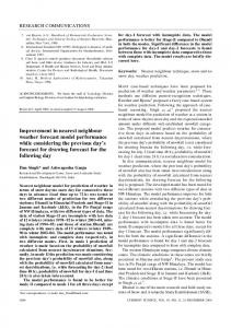
VII.
CONTROLLED SWAP
Performing a controlled swap of two large registers is slightly more difficult when only LNN interactions are available. The two registers need to be meshed so that pairs of equally significant qubits can be controlledswapped. The mesh circuit is shown in fig. 5. This circuit element would not be required in a general architecture. After the mesh circuit has been applied, the functional part of the controlled swap circuit (fig. 6) can be applied optimally with the control qubit moving from one end of the meshed registers to the other. The mesh circuit is then applied in reverse to untangle the two registers. The gate count and circuit depth of a mesh circuit is L(L − 1)/2 and L − 1 respectively. The corresponding equations for a complete LNN controlled swap are L2 + 5L and 6L. The general controlled swap only requires 6L gates and can be implemented in a circuit of depth 4L + 2. The controlled swap is the only part of this implementation of Shor’s algorithm that is significantly more difficult to implement on an LNN architecture.
VIII.
MODULAR MULTIPLICATION
The ideas behind the modular multiplication circuit of fig. 7 were discussed in section III. The first third
b’3
b’1 cswap
b1
a’0
b’2
b2
FIG. 5: Circuit designed to interleave two quantum registers.
b’ c
mesh
a2
a’
cswap
b3
c
cswap
a2
a.)
cswap
a3
cswap
a3
mesh
a3
mesh
a3
b’0 c
FIG. 6: a.) LNN circuit for the controlled swapping of two qubits |ai and |bi. The qubits |a′ i and |b′ i represent the potentially swapped states. b.) LNN circuit for the controlled swapping of two quantum registers. Note that when chained together, the effective depth of the cswap gate is 4.
comprises a controlled modular multiply (via repeated addition) with the result being stored in a temporary register. The middle third implements a controlled swap of registers. The final third resets the temporary register. Note that the main way in which the performance of the LNN circuit differs from the ideal general case is due to the inclusion of the two mesh circuits. Nearly all of the remaining swaps shown in the circuit do not contribute to the overall depth. Note that the two swaps drawn within the QFT and inverse QFT are intended to indicate the appending of a swap gate to the first and last compound gates in these circuits respectively. The total gate count for the LNN modular multiplication circuit is 4L3 + 20L2 + 58L − 2 versus the general gate count of 4L3 + 13L2 + 35L + 4. The LNN depth is 16L2 + 40L − 7 and the general depth 16L2 + 33L − 6. IX.
COMPLETE CIRCUIT
The complete circuit for Shor’s algorithm (fig. 8) can best be understood with reference to fig. 2a and the five steps described in section II. The last two steps of Shor’s algorithm are a QFT and measurement of the qubits involved in the QFT. When a 2-qubit controlled quantum gate is followed by measurement of the controlled qubit, it is equivalent to measure the control qubit first and then apply a classically controlled gate to the target qubit. If this is done to every qubit in fig. 2a, it can be seen that every qubit is decoupled. Furthermore, since the QFT is applied to the k register and the k register qubits are
φ (0)0
φ (0)1
φ (0)2
φ (0)3
φ (0)4
kx
ki
x(i+1)0
i
kx
φ (0)4
kx
φ (0)4
φ (0)0
ki ki
φ (0)0
x(i)0 x(i+1)0
φ (0)1
MS MS
φ (0)1
x(i)1 x(i+1)1
φ (0)2
x(i)2 x(i+1)2
φ (0)2
x(i)3 x(i+1)3
φ (0)3
m2 mod N
ki
φ (0)3
MS
x(i+1)1
x(i+1)2
x(i+1)3
7
i -1
x3ki - 2 (m2 ) mod N 3
i -1
x2ki - 2 (m2 ) mod N 2
i -1
x1ki - 2 (m2 ) mod N 0
i -1
kx
QFT
1
ki
x0
MS
x1
x2
x3
x0ki - 2 (m2 ) mod N
mesh cswap cswap
QFT-1
x1
x0
mesh
x2
x3
ki
cswap kx
MS
cswap
i
3 x3ki + 2 m2 mod N i
2 x2ki + 2 m2 mod N i
1 x1ki + 2 m2 mod N i
i
φ (0)0
φ (0)1
φ (0)2
φ (0)3
φ (0)4
kx
ki
x(i)0
MS
x(i)1
x(i)2
x(i)3
0 x0ki + 2 m2 mod N
FIG. 7: Circuit designed to modularly multiply x(i) by m2 if and only if ki = 1. Note that for simplicity the circuit for L = 4 has been shown. Note that the bottom L + 1 qubits are ancilla and as such start and end in the |φ(0)i state. The swap gates within the two QFT structures represent compound gates.
8 never interacted with one another, it is possible to arrange the circuit such that each qubit in the k register is sequentially used to control a modular multiplication, QFTed, then measured. Even better, after the first quit of the k register if manipulated in this manner, it can be reset and used as the second qubit of the k register. This one qubit trick [32] forms the basis of fig. 8. The total number of gates required in the LNN and general cases are 8L4 + 40L3 + 116 21 L2 + 4 12 L − 2 and 8L4 + 26L3 + 70 21 L2 + 8 21 L − 1 respectively. The circuit depths are 32L3 + 80L2 − 4L − 2 and 32L3 + 66L2 − 2L − 1 respectively. The primary result of this paper is that the gate count and depth equations for both architectures are identical to first order. X.
CONCLUSION
We have presented a circuit implementing Shor’s algorithm in a manner appropriate for a linear nearest neigh-
[1] P. W. Shor, Proceedings. Algorithmic Number Theory. First International Symposium, ANTS-I p. 289 (1994). [2] V. Subramaniam and P. Ramadevi, quant-ph/0210095 (2002). [3] N.-J. Wu et al., quant-ph/9912036 (1999). [4] R. Vrijen et al., Phys. Rev. A 62, 012306 (2000). [5] B. Golding and M. I. Dykman, cond-mat/0309147 (2003). [6] E. Novais and A. H. C. Neto, cond-mat/0308475 (2003). [7] L. C. L. Hollenberg et al., cond-mat/0306235 (2003). [8] L. Tian and P. Zoller, quant-ph/0306085 (2003). [9] K. Yang et al., Chinese Phys. Lett. 20, 991 (2003). [10] M. Feng et al., quant-ph/0304169 (2003). [11] J. K. Pachos and P. L. Knight, Phys. Rev. Lett. 91, 107902 (2003). [12] M. Friesen et al., Phys. Rev. B 67 (2003). [13] L. M. K. Vandersypen et al., quant-ph/0207059 (2002). [14] P. Solinas et al., Phys. Rev. B 67 (2003). [15] J. H. Jefferson et al., Phys. Rev. A 66 (2002). [16] D. Petrosyan and G. Kurizki, Phys. Rev. Lett. 89, 207902 (2002). [17] V. N. Golovach and D. Loss, Semicond. Sci. Tech. 17,
bour qubit array and studied the number of extra gates and consequent increase in circuit depth such a design entails. To first order our circuit involves 8L4 gates arranged in a circuit of depth 32L3 on 2L + 4 qubits — figures identical to that possible when interactions between arbitrary pairs of qubits are allowed. Given the importance of Shor’s algorithm, this result supports the widespread experimental study of linear nearest neighbour architectures.
Simulations of the robustness of the circuit when subjected to noise are in progress. Future simulations will investigate the performance of the circuit when protected by LNN quantum error correction.
355 (2002). [18] T. D. Ladd et al., Phys. Rev. Lett. 89, 017901 (2002). [19] V. V’yurkov and L. Y. Gorelik, quant-ph/0009099 (2000). [20] E. O. Kamenetskii and O. Voskoboynikov, condmat/0310558 (2003). [21] S. Beauregard, Quantum Inform. Compu. 3, 175 (2003). [22] R. L. Rivest et al., Communications of the ACM 21, 120 (1978). [23] V. Vedral et al., Phys. Rev. A 54, 147 (1996). [24] P. Gossett, quant-ph/9808061 (1998). [25] C. Zalka, quant-ph/9806084 (1998). [26] A. G. Fowler and L. C. L. Hollenberg, quant-ph/0306018 (2003). [27] B. Kraus and J. I. Cirac, Phys. Rev. A 63, 062309 (2001). [28] M. J. Bremner et al., Phys. Rev. Lett. 89, 247902 (2002). [29] C. D. Hill and H.-S. Goan, Phys. Rev. A 68 (2003). [30] B. E. Kane, Nature 393, 133 (1998). [31] A. G. Fowler et al., quant-ph/0311116 (2003). [32] S. Parker and M. B. Plenio, Phys. Rev. Lett. 85, 3049 (2000).
φ (0)2
φ (0)1
φ (0)0
0
0
0
φ (0)3
φ (0)4
kx
k8 Z1 H M8
x(8)0
MS
x(8)1
x(8)2
x(8)3
9
7
m2 mod N
k6
m2 mod N
k2
m2 mod N
k1
m2 mod N
k0
m2 mod N
Z 6 H M7 R H
k7
0
0
0
1 0 0 Phase: Z3
0 Reset: R
Mi
QFT
H
0
0
1
0
0
0
0
ith measurement
H M1 R H
1
0
1
0
Z1 H M2 R H
2
3 eiπM3M2M1/2 1
Z 2 H M3 R H
6
FIG. 8: Circuit designed to compute Shor’s algorithm. The single-qubit gates interleaved between the modular multiplications comprise a QFT that has been decomposed by using measurement gates to remove the need for controlled quantum phase rotations. Note that without these single-qubit gates the remaining circuit is simply modular exponentiation.