applications by porting a C compiler to the DISC processor. Justin Diether ...... integrated development of both the host program and the custom application 34].
IMPROVING FUNCTIONAL DENSITY THROUGH RUN-TIME CIRCUIT RECONFIGURATION
A Thesis Submitted to the Department of Electrical and Computer Engineering Brigham Young University
In Partial Ful llment of the Requirements for the Degree Doctor of Philosophy
c Michael J. Wirthlin 1997 by Michael J. Wirthlin November 1997
This dissertation by Michael J. Wirthlin is accepted in its present form by the Department of Electrical and Computer Engineering of Brigham Young University as satisfying the dissertation requirement for the degree of Doctorate of Philosophy.
Brad L. Hutchings Committee Chairman Brent E. Nelson Committee Member Brian D. Je�s Committee Member James K. Archibald Committee Member Doran Wilde Committee Member
Date
Michael D. Rice Graduate Coordinator
ii
ACKNOWLEDGMENTS This work was supported by the Defense Advanced Research Projects Agency (DARPA), Information Technology O�ce (ITO) under contract numbers DABT63-94-C-0085 and DABT63-96-C-0047. In addition, this e�ort is made possible by the work, inspiration, and contribution of many people. The assistance and ideas provided by my fellow graduate students within the BYU con gurable computing laboratory played an important role within this work. Jim Eldredge's original work on the run-time recon gured neural network provided the initial motivation and description of the bene ts and potential of runtime recon guration. Jim Hadley's follow-up to the RRANN project successfully demonstrated the advantages of exploiting partial recon guration. The meticulous low-level design of his project provided the motivation needed to explore other unique uses of partial recon guration. Dave Clark eased the development of DISC applications by porting a C compiler to the DISC processor. Justin Diether assisted in the design, hand-layout, and testing of many partially recon gured circuits. I would also like to thank Paul Graham for his generous assistance and support of our many mutual activities, classes, and projects at BYU. Other graduate students assisting me with this work include Russel Peterson, Mike Rencher, Richard Ross, and Peter Bellows. My advisor, Brad Hutchings, provided essential assistance and encouragement in all of the projects, ideas, and results presented within this work. My decision to complete this degree and write this dissertation was in uenced largely by his advice and positive encouragement. Brent Nelson and other faculty members within the Electrical and Computer Engineering department at BYU have provided critical feedback on a wide variety of topics relating to this work. I would also like to acknowledge the insight and assistance of many collaborators researching closely related subjects. Fortunately, the research community investigating con gurable computing machines is a very open and friendly group of people eager to share information and assist others. Speci cally, the members of the Soft Logic group at National Semiconductor provided essential device, tool, and support assistance needed to successfully complete several projects contained within this work. The support of my family was critical for the successful completion of this work. My parents have provided continual support and motivation for my pursuit of higher education and have set high standards for education and learning. Most importantly, I would like to acknowledge and thank my wife, RayAnne, and my children for their patience and support of my academic interests. RayAnne provided essential encouragement throughout my graduate education and assisted in the nal editing of this work. iii
Contents Acknowledgments 1 Introduction
1.1 Custom Computing Machines . . . . . . . . . . . . . . . . . . . . . 1.2 Run-Time Recon guration . . . . . . . . . . . . . . . . . . . . . . . 1.3 Thesis Organization . . . . . . . . . . . . . . . . . . . . . . . . . . .
2 Con gurable Computing Machines
2.1 Recon gurable Computing . . . . . . . . . . 2.1.1 Custom Computing Machines . . . . 2.1.2 DEC PeRLe . . . . . . . . . . . . . . 2.1.3 SRC SPLASH . . . . . . . . . . . . . 2.2 Specialization Techniques . . . . . . . . . . . 2.2.1 Customization of Functional Units . 2.2.2 Exploitation of Concurrency . . . . . 2.2.3 Optimized Communication Networks 2.2.4 Custom I/O Interfaces . . . . . . . . 2.3 Summary . . . . . . . . . . . . . . . . . . .
. . . . . . . . . .
3 Run-Time Recon guration
. . . . . . . . . .
. . . . . . . . . .
. . . . . . . . . .
3.1 Opportunities for Run-Time Specialization . . . . . 3.1.1 Temporal Locality . . . . . . . . . . . . . . 3.1.2 Partitioning of Large Systems . . . . . . . . 3.2 Run-Time Recon gured Applications . . . . . . . . 3.2.1 Arti cial Neural Network . . . . . . . . . . . 3.2.2 Video Coding . . . . . . . . . . . . . . . . . 3.2.3 Variable-Length Code Detection . . . . . . . 3.2.4 Automatic Target Recognition . . . . . . . . 3.2.5 Stereo Vision . . . . . . . . . . . . . . . . . 3.2.6 Dynamic Instruction Set Computer (DISC) . 3.3 Con guration Overhead . . . . . . . . . . . . . . .
. . . . . . . . . .
. . . . . . . . . .
. . . . . . . . . .
. . . . . . . . . .
. . . . . . . . . .
. . . . . . . . . .
. . . . . . . . . .
. . . . . . . . . .
. . . . . . . . . . .
. . . . . . . . . . .
. . . . . . . . . . .
. . . . . . . . . . .
. . . . . . . . . . .
. . . . . . . . . . .
. . . . . . . . . . .
. . . . . . . . . . .
4.1 Functional Density . . . . . . . . . . . . . . . . . . . . 4.2 Functional Density of Run-Time Recon gured Systems 4.3 Architectural Analysis . . . . . . . . . . . . . . . . . . 4.3.1 Application-Speci c Circuit Parameters . . . . . 4.3.2 Comparing Functional Density . . . . . . . . . .
. . . . .
. . . . .
. . . . .
. . . . .
. . . . .
. . . . .
. . . . .
4 Analysis of Run-Time Recon gured Systems
iv
. . . . . . . . . . .
. . . . . . . . . .
iii 1 2 3 5
7
8 9 10 11 13 13 15 16 16 17
19 20 20 22 27 27 28 29 30 31 32 32
34 34 37 40 41 42
5 Applications
5.1 Run-Time Recon gured Arti cial Neural-Network . . . . . . 5.1.1 RRANN System Architecture . . . . . . . . . . . . . 5.1.2 Performance . . . . . . . . . . . . . . . . . . . . . . . 5.1.3 Area Cost . . . . . . . . . . . . . . . . . . . . . . . . 5.1.4 Functional Density . . . . . . . . . . . . . . . . . . . 5.1.5 Con guration Overhead . . . . . . . . . . . . . . . . 5.2 Partially Run-Time Recon gured Arti cial Neural-Network . 5.2.1 Partial Con guration . . . . . . . . . . . . . . . . . . 5.2.2 Performance . . . . . . . . . . . . . . . . . . . . . . . 5.2.3 Area Cost . . . . . . . . . . . . . . . . . . . . . . . . 5.2.4 Functional Density . . . . . . . . . . . . . . . . . . . 5.2.5 Con guration Overhead . . . . . . . . . . . . . . . . 5.3 Template Matching . . . . . . . . . . . . . . . . . . . . . . . 5.3.1 System Architecture . . . . . . . . . . . . . . . . . . 5.3.2 Performance . . . . . . . . . . . . . . . . . . . . . . . 5.3.3 Area Cost . . . . . . . . . . . . . . . . . . . . . . . . 5.3.4 Functional Density . . . . . . . . . . . . . . . . . . . 5.3.5 Con guration Overhead . . . . . . . . . . . . . . . . 5.4 Sequence Comparison . . . . . . . . . . . . . . . . . . . . . . 5.4.1 Limited Hardware Systems . . . . . . . . . . . . . . . 5.4.2 Run-Time Recon guration of Edit-Distance PEs . . . 5.4.3 Functional Density . . . . . . . . . . . . . . . . . . . 5.5 Application Summary . . . . . . . . . . . . . . . . . . . . .
6 Dynamic Instruction Set Computer (DISC)
. . . . . . . . . . . . . . . . . . . . . . .
. . . . . . . . . . . . . . . . . . . . . . .
6.1 Functional Density of DISC Instructions . . . . . . . . . . . . . 6.1.1 Functional Density of the Static Processor Core . . . . . 6.1.2 Functional Density of Custom Instructions . . . . . . . . 6.1.3 Low-Pass Filter . . . . . . . . . . . . . . . . . . . . . . . 6.1.4 Maximum Value Search . . . . . . . . . . . . . . . . . . 6.2 Improving Functional Density by Exploiting Temporal Locality . 6.2.1 Functional Density of the DISC Instruction Cache . . . . 6.2.2 Measuring Hit Rate . . . . . . . . . . . . . . . . . . . . . 6.2.3 Example Hit Rate Function . . . . . . . . . . . . . . . . 6.2.4 Example Functional Density Calculation . . . . . . . . . 6.2.5 Functional Density of a DISC Program . . . . . . . . . . 6.3 Summary . . . . . . . . . . . . . . . . . . . . . . . . . . . . . .
7 Recon guration Time
. . . . . . . . . . . . . . . . . . . . . . . . . . . . . . . . . . .
. . . . . . . . . . . . . . . . . . . . . . . . . . . . . . . . . . .
46 46 47 48 50 52 53 56 58 59 60 61 62 66 68 72 73 73 74 77 78 80 82 88
90
91 92 92 95 100 106 107 108 111 113 116 119
121
7.1 Con guration of Conventional FPGAs . . . . . . . . . . . . . . . . 121 7.1.1 Con guration Bandwidth, � . . . . . . . . . . . . . . . . . . 122 v
7.1.2 Con guration Length, L . . . . . . . . . . 7.2 Con guration Improvement Techniques . . . . . . 7.2.1 Improving the Con guration Bandwidth . 7.2.2 Partial Con guration . . . . . . . . . . . . 7.2.3 Simultaneous Con guration and Execution 7.2.4 Exploiting Temporal Locality . . . . . . . 7.2.5 Distributed Con guration . . . . . . . . . 7.3 Summary . . . . . . . . . . . . . . . . . . . . . .
8 Conclusions
8.1 Review . . . . . . . . . . . . . . . 8.1.1 Run-Time Recon guration 8.1.2 Functional Density . . . . 8.1.3 Con guration Time . . . . 8.2 Future Work . . . . . . . . . . . .
. . . . .
. . . . .
. . . . .
. . . . .
. . . . .
. . . . .
. . . . .
. . . . .
. . . . .
. . . . . . . . . . . . .
. . . . . . . . . . . . .
. . . . . . . . . . . . .
. . . . . . . . . . . . .
. . . . . . . . . . . . .
. . . . . . . . . . . . .
. . . . . . . . . . . . .
. . . . . . . . . . . . .
. . . . . . . . . . . . .
. . . . . . . . . . . . .
126 128 129 131 133 136 143 144
146
146 146 148 148 149
A Special-Purpose Bit-Serial Template Matching Circuit
152
B Edit-Distance Algorithm
164
A.1 Propagating Template Constants . . . . . . . . . . . . . . . . . . . 159 A.2 CLAy Implementation . . . . . . . . . . . . . . . . . . . . . . . . . 161 A.3 Functional Density . . . . . . . . . . . . . . . . . . . . . . . . . . . 162 B.1 Unidirectional Array . . . . . . . . . . . . B.2 Specialization of the Unidirectional Array B.3 Mapping to the CLAy FPGA . . . . . . . B.3.1 Distance Unit . . . . . . . . . . . . B.3.2 General-Purpose Matching Unit . . B.3.3 Special-Purpose Matching Unit . . B.4 Functional Density . . . . . . . . . . . . .
C DISC Reference
C.1 DISC Architecture . . . . . . . C.1.1 DISC Processor Core . . C.1.2 Custom Instructions . . C.1.3 Partial Recon guration . C.1.4 Relocatable Hardware . C.2 Application Example . . . . . . C.2.1 Object Thinning . . . . C.2.2 Run-Time Execution . . C.2.3 Execution Results . . . .
D Con guration Data
. . . . . . . . .
. . . . . . . . .
. . . . . . . . .
. . . . . . . . .
. . . . . . . . .
. . . . . . . . .
. . . . . . . . . . . . . . . .
. . . . . . . . . . . . . . . .
. . . . . . . . . . . . . . . .
. . . . . . . . . . . . . . . .
. . . . . . . . . . . . . . . .
. . . . . . . . . . . . . . . .
. . . . . . . . . . . . . . . .
. . . . . . . . . . . . . . . .
. . . . . . . . . . . . . . . .
. . . . . . . . . . . . . . . .
. . . . . . . . . . . . . . . .
. . . . . . . . . . . . . . . .
. . . . . . . . . . . . . . . .
. . . . . . . . . . . . . . . .
165 167 168 169 170 170 171
181
183 186 186 189 190 194 195 198 200
203 vi
List of Tables 2.1 2.2 4.1 5.1 5.2 5.3 5.4 5.5 5.6 5.7 5.8 5.9 5.10 5.11 5.12 6.1 6.2 6.3 6.4 6.5 6.6 6.7 7.1 7.2 7.3 7.4 A.1 B.1 B.2 C.1 C.2 C.3 D.1 D.2 D.3 D.4
DEC PeRLe Applications. . . . . . . . . . . . . . . . . . . . . . . . SPLASH Applications. . . . . . . . . . . . . . . . . . . . . . . . . . Example Circuit Parameters and Functional Density. . . . . . . . . RRANN Circuit Parameters. . . . . . . . . . . . . . . . . . . . . . . Circuit Parameters for a 60 Neuron Network. . . . . . . . . . . . . . Con guration Overhead of a 60 Neuron Network. . . . . . . . . . . RRANN Circuit Parameters. . . . . . . . . . . . . . . . . . . . . . . RRANN-II Circuit Parameters for a 60 Neuron Network. . . . . . . RRANN-II Partial Bit-Stream Sizes. . . . . . . . . . . . . . . . . . Improvement in Functional Density of RRANN-II. . . . . . . . . . . Circuit Parameters of the Correlation PE. . . . . . . . . . . . . . . Functional Density of Template Matching Circuit . . . . . . . . . . Con guration Overhead of a Template Matching Circuit. . . . . . . Comparison of Two Edit Distance Alternatives. . . . . . . . . . . . Application Summary. . . . . . . . . . . . . . . . . . . . . . . . . . Area of Static Processor Core. . . . . . . . . . . . . . . . . . . . . . Con guration Rate of DISC. . . . . . . . . . . . . . . . . . . . . . . Maximum Functional Density of the Maximum Value Custom Instruction. . . . . . . . . . . . . . . . . . . . . . . . . . . . . . . . . Con guration Time and Con guration Ratio of the Maximum Value Search Custom Instruction. . . . . . . . . . . . . . . . . . . . . . . Sample DISC Instruction Sizes. . . . . . . . . . . . . . . . . . . . . Distances of Instruction INSTA within Listing 6.4. . . . . . . . . . . Hit Rate of Instructions within Listing 6.4. . . . . . . . . . . . . . . FPGA Device Con guration Bandwidth. . . . . . . . . . . . . . . . Xilinx XC3000 Con guration Data. . . . . . . . . . . . . . . . . . . Improvement in Functional Density for Several Partially Recon gured Systems. . . . . . . . . . . . . . . . . . . . . . . . . . . . . . . Con guration Overhead and Hit Rate Bounds for Two Values of �. Correlation Cell Parameters. . . . . . . . . . . . . . . . . . . . . . . Area and Time Comparison of Edit-Distance Components . . . . . Functional Density of General and Special Purpose Edit Distance PEs . . . . . . . . . . . . . . . . . . . . . . . . . . . . . . . . . . . Run-Time Composition of Sample DISC Instructions. . . . . . . . . DISC and 486 PC Execution Time. . . . . . . . . . . . . . . . . . . DISC Custom Instructions. . . . . . . . . . . . . . . . . . . . . . . . Lucent ORCA 2xx Series FPGA Con guration Data. . . . . . . . . Altera FLEX 8000 Con guration Data. . . . . . . . . . . . . . . . . Altera FLEX 10K Con guration Data. . . . . . . . . . . . . . . . . Xilinx XC3000 Con guration Data. . . . . . . . . . . . . . . . . . . vii
11 12 43 51 53 54 61 63 64 65 71 74 76 86 88 92 94 104 105 112 112 117 123 126 132 143 163 171 173 185 201 202 203 203 204 204
D.5 D.6 D.7 D.8 D.9
Xilinx XC4000 Con guration Data. . . . . . . . . . Xilinx XC4000EX Con guration Data. . . . . . . . Xilinx XC6200 Family Con guration Data. . . . . . Atmel AT6000 Family Con guration Data. . . . . . National Semiconductor CLAy Con guration Data.
viii
. . . . .
. . . . .
. . . . .
. . . . .
. . . . .
. . . . .
. . . . .
. . . . .
. . . . .
205 205 205 206 206
List of Figures 2.1 2.2 2.3 3.1 3.2 3.3 3.4 3.5 3.6 3.7 3.8 3.9 4.1 4.2 5.1 5.2 5.3 5.4 5.5 5.6 5.7 5.8 5.9 5.10 5.11 5.12 5.13 5.14 5.15 5.16 6.1 6.2 6.3 6.4 6.5 6.6 6.7 6.8
DEC PeRLe-1. . . . . . . . . . . . . . . . . . . . . . . . . . . . . . 10 SRC SPLASH 2 . . . . . . . . . . . . . . . . . . . . . . . . . . . . . 12 Signal-Flow Graph of Newton's Mechanics Problem. . . . . . . . . . 17 Three Stages of the Backpropagation Training Algorithm. . . . . . . 21 Run-Time Recon guration of Special-Purpose Neuron Processors. . 22 Signal-Flow Graph of a Concurrent FIR Filter. . . . . . . . . . . . . 24 Constant Propagated Special-Purpose FIR Filter. . . . . . . . . . . 25 Partitioning of the FIR Circuit. . . . . . . . . . . . . . . . . . . . . 25 Run-Time Recon guration of FIR Filter Taps. . . . . . . . . . . . . 26 Video Coding Algorithm. . . . . . . . . . . . . . . . . . . . . . . . . 28 Sample Hardwired Decoding Tree. . . . . . . . . . . . . . . . . . . . 29 Merging of Similar Templates . . . . . . . . . . . . . . . . . . . . . 31 Degradation of Functional Density . . . . . . . . . . . . . . . . . . 40 Example Functional Density Comparison. . . . . . . . . . . . . . . . 44 System Architecture of RRANN. . . . . . . . . . . . . . . . . . . . 48 Con guration Overhead of RRANN. . . . . . . . . . . . . . . . . . 55 Functional Density of RRANN. . . . . . . . . . . . . . . . . . . . . 57 Con guration Overhead of RRANN-II. . . . . . . . . . . . . . . . . 66 Functional Density of RRANN-II. . . . . . . . . . . . . . . . . . . . 67 Parallel Computation of Correlation. . . . . . . . . . . . . . . . . . 69 Array of Correlation PEs Programmed to a Speci c Template Image. 70 General-Purpose Conditional Bit-Serial Adder. . . . . . . . . . . . . 70 Special-Purpose Conditional Adders. . . . . . . . . . . . . . . . . . 71 Partial Con guration of Correlation Array. . . . . . . . . . . . . . . 75 Functional Density of Template Matching Circuit as a Function of Image Size. . . . . . . . . . . . . . . . . . . . . . . . . . . . . . . . 77 Partitioning of a Systolic Edit Distance Array. . . . . . . . . . . . . 79 Bu�ering of Partial Results Using FIFOs. . . . . . . . . . . . . . . . 80 Execution Sequence of Partitions. . . . . . . . . . . . . . . . . . . . 81 Execution and Con guration of Special-Purpose PEs. . . . . . . . . 82 Functional Density of Edit Distance Circuit as a Function of Character Length. . . . . . . . . . . . . . . . . . . . . . . . . . . . . . . 87 Data Flow of MEAN Instruction Module. . . . . . . . . . . . . . . . . 97 Architectural Overview of the Low-Pass Instruction Module. . . . . 98 Functional Density of a Low-Pass Filter . . . . . . . . . . . . . . . . 100 Maximum Value Instruction | Block Diagram. . . . . . . . . . . . 103 Functional Density of the Maximum Value Instruction. . . . . . . . 106 Sample Instruction Sequence. . . . . . . . . . . . . . . . . . . . . . 110 Hit Rate of INSTA as a Function of Instruction Cache Size. . . . . . 113 Functional Density of INSTA as a Function of Instruction Cache Size. 114 ix
6.9 Functional Density of INSTA for the LRU and Optimal Replacement Policies. . . . . . . . . . . . . . . . . . . . . . . . . . . . . . . . . . 115 6.10 Functional Density of INSTA with a Low Con guration Ratio. . . . 116 6.11 Functional Density of Listing 6.4 Based on Cache Size. . . . . . . . 118 7.1 Improvement Limitations Based on a Constant Con guration Time. 125 7.2 Reduction in Functional Density for Larger FPGA devices. . . . . . 128 7.3 Limitations on Area Overhead for Con guration Improvements. . . 130 7.4 Maximum Allowable Area for a 563 MB/sec Con guration Interface. 131 7.5 Simultaneous Execution and Con guration Using Two FPGAs. . . . 134 7.6 Maximum � as a Function of f . . . . . . . . . . . . . . . . . . . . . 135 7.7 Multiple FPGA Resources Interconnected to Form a Con guration Cache. . . . . . . . . . . . . . . . . . . . . . . . . . . . . . . . . . . 138 7.8 RRANN Neural Processor Cache. . . . . . . . . . . . . . . . . . . . 139 7.9 Functional Density of Cached RRANN System as a Function of Network Size. . . . . . . . . . . . . . . . . . . . . . . . . . . . . . . 141 7.10 Multiple Context FPGA. . . . . . . . . . . . . . . . . . . . . . . . . 141 A.1 Binary Template Correlation PE. . . . . . . . . . . . . . . . . . . . 153 A.2 Correlation Column Processor. . . . . . . . . . . . . . . . . . . . . . 154 A.3 Parallel Computation Using Column Processors. . . . . . . . . . . . 155 A.4 Spatial Organization of the Correlation PE. . . . . . . . . . . . . . 156 A.5 Retimed Processor Array. . . . . . . . . . . . . . . . . . . . . . . . 157 A.6 Bit-Serial Correlation PE. . . . . . . . . . . . . . . . . . . . . . . . 157 A.7 Proper Data Alignment of Bit-Serial Correlation PEs. . . . . . . . . 158 A.8 Special-Purpose Bit-Serial Correlation PEs. . . . . . . . . . . . . . 160 A.9 Special-Purpose Array of Correlation PEs. . . . . . . . . . . . . . . 160 A.10 Physical Bit-Serial Adder Layout. . . . . . . . . . . . . . . . . . . . 161 A.11 Physical Layout of Bit-Serial Add by \1". . . . . . . . . . . . . . . 162 B.1 Dependency Graph of Edit Distance Calculation. . . . . . . . . . . 165 B.2 Projection and Hyper-planes of Unidirectional Array. . . . . . . . . 166 B.3 Signal-Flow Graph of Unidirectional Array. . . . . . . . . . . . . . . 166 B.4 Block Diagram of Unidirectional PE. . . . . . . . . . . . . . . . . . 167 B.5 General-Purpose Matching Unit. . . . . . . . . . . . . . . . . . . . . 167 B.6 Special-Purpose Matching Unit. . . . . . . . . . . . . . . . . . . . . 168 B.7 Constant Propagated Processing Element. . . . . . . . . . . . . . . 168 B.8 Customized Source Sequence Processor Array. . . . . . . . . . . . . 169 B.9 Distance Unit Schematic. . . . . . . . . . . . . . . . . . . . . . . . . 173 B.10 Layout of CLAy Distance Unit. . . . . . . . . . . . . . . . . . . . . 174 B.11 General-Purpose Matching Unit Schematic. . . . . . . . . . . . . . . 174 B.12 General-Purpose Matching Unit Layout. . . . . . . . . . . . . . . . 175 B.13 Special-Purpose Matching Unit Schematic (0011). . . . . . . . . . . 176 B.14 Special-Purpose Matching Unit Layout. . . . . . . . . . . . . . . . . 177 B.15 Worst-Case Special-Purpose Matching Unit Layout. . . . . . . . . . 178 x
B.16 General-Purpose Edit-Distance PE Layout. . . . . . . . . . . . B.17 Special-Purpose Edit-Distance PE Layout. . . . . . . . . . . . C.1 DISC Architecture: Processor Core and Recon gurable Logic. C.2 DISC Processor Core. . . . . . . . . . . . . . . . . . . . . . . . C.3 Relocation of Irregular Shaped 2-D Custom Instructions. . . . C.4 Linear Hardware Space with Communication Network. . . . . C.5 Constrained Instruction Module. . . . . . . . . . . . . . . . . . C.6 Multiple Instructions within Linear Hardware Space. . . . . . C.7 DISC Instruction Execution. . . . . . . . . . . . . . . . . . . . C.8 Object Thinning Steps. . . . . . . . . . . . . . . . . . . . . . . C.9 DISC State After Executing HISTOGRAM. . . . . . . . . . . . . C.10 DISC State After Executing Threshold Value Subroutine. . . . C.11 DISC Executing the SKELETONIZATION Instruction. . . . . . .
xi
. . . . . . . . . . . . .
. . . . . . . . . . . . .
. . . . . . . . . . . . .
179 180 183 187 191 192 193 194 195 197 199 200 200
Improving Functional Density Through Run-Time Circuit Recon guration Michael J. Wirthlin
Chapter 1
INTRODUCTION Programmable logic devices are common building-blocks within many digital systems. As the name implies, these logic devices are user programmable or programmable after device manufacturing. The use of user programmable logic allows circuit designers to enjoy the bene ts of circuit customization without the non-recurring engineering (NRE) fees typically associated with custom silicon devices. In addition, the use of programmable logic shrinks the development cycle of custom circuits by removing the time-consuming step of circuit manufacturing. A rapidly growing segment of the programmable logic market includes eld-programmable gate arrays (FPGAs). As the name implies, these devices provide an array of \gates" or logic resources that are surrounded by a rich interconnection network. Much like a conventional gate array, FPGAs provide considerably more logic than is available with discrete logic components. Unlike a gate array, which requires custom manufacturing, an FPGA is programmable by the end user. Several good publications provide a description of commercial FPGA technology, architectures, and design styles [1, 2, 3]. Although all FPGAs can be programmed by the user at least once, many FPGA families allow reprogramming of the logic resources. These FPGAs, based on static memory technology, are programmed and reprogrammed by loading a circuit \bit-stream" into the internal con guration memory. Although the static con guration memory is volatile and loses its con guration state without power, it allows unlimited recon guration of the device. This recon gurability can be exploited in the following novel ways: � Logic Prototyping, � Multi-Purpose Hardware, and � Con gurable Computing.
Logic Prototyping Perhaps the most common use of this recon gurability is within circuit prototyping environments. A single FPGA device can be used to test 1
a circuit as it progresses through the development phase. Circuit improvements or changes are easily accommodated on the FPGA through recon guration. Unlike the fabrication of a custom device, there are no risks involved with recon guring a circuit onto an FPGA. Errors found within the circuit can be modi ed and con gured without any additional fabrication costs. The ability to prototype arbitrary digital circuits within FPGAs has motivated the use of FPGAs as key components within logic emulation systems [4].
Multi-Purpose Hardware The recon gurability of an FPGA o�ers more than
increased exibility and risk reduction - recon guration provides unique opportunities for hardware reuse. A single FPGA device can operate as several di�erent circuits as needed by a system. For example, an FPGA can be con gured to perform system diagnostics at power-up [5]. Once diagnostics are complete, the FPGA is recon gured to perform its standard operational functions. This dual-use of the FPGA device allows a system to operate with fewer resources than possible with a non-con gurable system. Other examples of hardware reuse include adaptive systems and multi-mode hardware interfaces [6].
Con gurable Computing Circuit recon gurability also allows FPGAs to op-
erate as custom \computers". Application circuits, designed to perform some computation within the FPGA logic resources, are con gured onto an FPGA much like a software program is loaded within the memory of a processor. Since the FPGA resources are recon gurable, any number of such circuit con gurations can be executed within an FPGA resource. Many con gurable computing systems have been designed and used to solve a wide range of application-speci c problems. Several conferences and workshops, organized to investigate FPGA technology and FPGA based computers, provide ample examples of such computing structures [7, 8, 9]. In addition, several recent articles in popular trade magazines report on the growing use of this technology in commercial systems [10, 11, 12].
1.1 Custom Computing Machines Computing architectures designed within FPGA resources are often called custom computing machines or CCMs. Other names include recon gurable 2
computers, adaptive computing systems, or transformable computers. These machines are aptly termed computers due to their recon gurability and computational capabilities. Through recon guration, an application-speci c circuit used to perform one computation can be replaced with an application-speci c circuit performing a di�erent and possibly unrelated computation. Unlike traditional computers, the structures used to perform a computation within a CCM can be specialized to the computational task at hand. Such architectural specialization allows a CCM system to provide unusually ef cient computational structures. Surprisingly few FPGA resources can be used to solve many important computationally challenging problems by optimizing the datapath, control, and communication network at the gate-level. The more the computing structure is specialized to the computation of interest, the greater its e�ciency and performance. The computational e�ciency provided by architectural specialization allows a modest array of FPGA devices to achieve surprising levels of performance. Several CCM applications have demonstrated performance superior to high-end workstations and even supercomputers [13]. Application examples demonstrating such impressive performance include genetic database searching [14], long integer multiplication [15], volume visualization [16], real-time image processing [17], and RSA cryptography [18]. Even small arrays of FPGAs, including those with only a single device, have been shown to provide superior performance over other more costly alternatives [19, 20, 21, 22].
1.2 Run-Time Recon guration The bene ts of e�ciency and performance provided by architectural specialization can be extended by specializing a computing architecture at runtime. Such dynamic circuit specialization is possible by recon guring the FPGA resources at run-time. This technique, often called run-time recon guration (RTR) [23, 24], provides additional opportunities for circuit specialization that are unavailable within static systems. Several CCM applications demonstrate improved hardware e�ciency by specializing circuits at run-time. A neural-network application, for example, 3
increases the e�ciency of its FPGA hardware by removing idle circuits at run-time [23]. An image processing system uses a similar technique to optimize its hardware resources between one of several image processing algorithms [25]. These and other examples achieve greater levels of e�ciency by specializing its FPGA resources at run-time based on the dynamic conditions of the system. Although RTR has been shown to improve the e�ciency of a computation, additional time is required for con guring circuit resources during execution. Unlike most CCM applications in which recon guration occurs o�-line or before a computation takes place, RTR requires con guration to occur on-line or during circuit execution. With currently available devices, recon guration time is on the order of milli-seconds | often orders of magnitude greater than the time required to complete an individual computation. In many cases, this lengthy con guration time clearly mitigates the advantages of RTR. For other cases, however, this trade-o� is not so clear. The use of RTR involves a trade-o� between a reduction in hardware and the penalty of recon guration time. In practice, RTR should be used if some net advantage over a more traditional static approach can be shown. To date, no general quantitative method has been suggested to balance the advantages of RTR with its associated con guration costs. This dissertation will address this issue by introducing and using a costsensitive metric that balances the advantages of run-time recon guration against the added cost of con guration time. This metric will be used to address the following important questions:
� How sensitive to con guration time are RTR applications? � How can the use of RTR, including its associated con guration time, be
justi ed over conventional static methods? � When is RTR appropriate within an application? � What are the composite bene ts of a technique that improves con guration time?
4
1.3 Thesis Organization This dissertation will commence by introducing application-speci c computing in Chapter 2. Application-speci c computing architectures achieve impressive levels of performance and e�ciency by specializing all aspects of the computing structure to the application of interest. Several architectural specialization techniques will be presented to demonstrate these advantages. The advantages of using FPGA technology for application-speci c computing will be described along with several examples. Chapter 3 will follow by introducing run-time recon guration (RTR). Speci cally, this chapter will describe how additional opportunities for specialization can be exploited by recon guring circuit resources at run-time. Several published examples of RTR will demonstrate the use of these techniques in working systems. Chapter 4 will continue by introducing a method of measuring the advantages obtained by run-time circuit specialization. This metric, called functional density, balances the improvements in area and execution time provided by run-time circuit specialization against the added overhead of con guration time. Chapter 5 will apply this functional density metric to several applications exploiting RTR. The functional density of each RTR application will be compared to the functional density of the same application operating within a conventional static environment. Such a comparison will indicate the appropriateness of RTR and identify the conditions in which RTR is justi ed. The applications used in the analysis include two variations of an arti cial neural network, a template matching circuit, and a sequence matching circuit. Several appendices are included to provide the details of these applications. Chapter 6 will follow by analyzing the e�ects of run-time recon guration within the Dynamic Instruction Set Computer. Using the functional density metric, the bene ts of recon guring special-purpose processor instructions will be balanced against the associated recon guration overhead. Chapter 7 will address the importance of recon guration time and review the performance of conventional con guration methods. Since most commercially available FPGAs provide relatively slow con guration interfaces, several con guration improvement techniques will be reviewed. These techniques include 5
partial con guration, simultaneous execution and con guration, exploitation of temporal locality, and distributed con guration. Chapter 8 will conclude by summarizing the results of this analysis.
6
Chapter 2
CONFIGURABLE COMPUTING MACHINES There are many computationally challenging problems with real-time computing requirements that are too demanding for general-purpose programmable processors. The computational requirements of operations such as real-time video compression, image processing, and three-dimensional graphics often exceed billions of operations per second. Computing architectures solving these challenging problems must handle an enormous amount of data while simultaneously performing the computation. The computational capability and I/O sub-systems of general-purpose processors are insu�cient for the demands placed by these and other real-time computing challenges. Application-speci c computing architectures are often used to solve such computationally and I/O intensive operations. These architectures perform such demanding real-time operations by specializing the computing structure to the application problem of interest. All aspects of a computing architecture, including the functional units, I/O interfaces, control, and memory, are optimized to perform the operation as e�ciently as possible. For example, a custom device designed solely to compute the Fast Fourier Transform (FFT) achieves signi cantly greater performance and e�ciency than other more general-purpose approaches [26]. However, application-speci c architectures are poorly suited for solving computing problems outside of their intended application area. The custom FFT device, for example, is incapable of performing any computation other than the FFT for which it was designed. If operations other than the FFT must be performed by the same system, such a highly specialized device cannot be used. The use of these highly specialized devices is also discouraged for economic reasons. In many cases, an application-speci c architecture is so specialized and of such limited appeal that its design and manufacturing costs cannot be justi ed. Because of this in exibility, few devices are specialized with only a single operation in mind. Instead, application-speci c architectures routinely sacri ce the performance and e�ciency provided by architectural specialization for greater 7
exibility. Programmable architectures are particularly attractive since the function can be changed by updating the executing program. The programmability of a digital signal processor (DSP), for example, is often more attractive for the computation of the FFT than a higher performance custom device. The same DSP used to compute the FFT can be used to perform countless other important signal processing functions. The use of architectural specialization techniques involves a classic tradeo� between improvements in e�ciency and loss of exibility. The more specialized an architecture is to an application, the greater its e�ciency and performance. At the same time, such specialized architectures are less exible and less useful to other unrelated application areas. The lack of exibility found within specialpurpose architectures limits the extent to which architectural specialization can take place. As the following quotation suggests, architectural specialization within special-purpose architectures is most often limited by economic factors rather than technical advantages: \A fundamental factor in any tool-building enterprise is the trade-o� between generality and performance. In almost all cases, a generalpurpose tool is less cost-e�ective in a particular case than is a tool designed especially for that case. In practice, this trade-o� is usually decided by economic factors: the extra (per application) design cost of a special-purpose device is balanced against the lower e�ciency of a general-purpose device." [27] Many of these limitations can be overcome by exploiting the recon gurability of FPGAs. This chapter will describe how circuit recon gurability allows application-speci c architectures to achieve greater levels of specialization than static, full-custom alternatives. Two con gurable computing examples will be presented to demonstrate this important principle. Finally, several important specialization techniques used by these CCM systems will be reviewed.
2.1 Recon gurable Computing The economic factors limiting specialization can be overcome by exploiting the recon gurability of SRAM based FPGAs [28]. As described in Section 1.2, 8
an FPGA provides unlimited recon guration of its logic resources [29]. Through circuit recon guration, a wide variety of application-speci c circuits can be con gured and recon gured within the same FPGA resource. Unlike custom VLSI architectures that add general-purpose architectural features to preserve exibility, FPGA based systems provide exibility in the form of circuit recon guration. Circuit recon gurability allows the development of application-speci c architectures and the exploitation of unique specialization techniques that are unjusti able within custom silicon devices. For example, many application-speci c computing architectures lack su�cient market interest to justify development within a custom device. These same architectures, however, can be justi ed within an FPGA since the FPGA can always be recon gured as another more useful architecture at a later time. The recon gurability of FPGAs allows the development of very specialized computing architectures while preserving the architectural exibility demanded by economic constraints. This exibility is exploited within several computing machines based on recon gurable FPGAs. These architectures, called \custom computing machines" or CCMs, organize FPGA resources with memory and I/O interfaces for the purpose of application-speci c computing. CCMs provide the exibility of a traditional computer by allowing circuit recon guration | any number of applicationspeci c computing circuits can be \programmed" onto the CCM through recon guration. At the same time, CCMs preserve the e�ciency and performance of specialpurpose architectures by allowing ne-grain circuit specialization. Recon guration of FPGA resources within CCMs combines the exibility of programmable architectures with the e�ciency and high performance of application-speci c architectures.
2.1.1 Custom Computing Machines Several successful CCM systems have demonstrated signi cant performance and computational e�ciency for a wide range of applications. These systems achieve such high levels of performance by \executing" a custom, highly specialized computing architecture for each problem of interest. The functional units, data path, control, and I/O interfaces are all optimized to each application-speci c 9
computing architecture operating within the system. Two of the most successful CCM systems include the DECPeRLe developed at Digital Equipment Corporation's Paris Research Laboratory [30], and the SPLASH system developed at the Supercomputer Research Center [31]. Both systems demonstrate signi cant performance improvements for many applications and continue to be used in the research community. Each of these two CCMs will be introduced along with a brief description of their associated application examples.
2.1.2 DEC PeRLe The PeRLe-0 and and its successor, the PeRLe-1, demonstrate signi cant performance over a surprisingly wide range of computing problems [30, 32, 33]. These architectures comprise a two dimensional mesh of FPGAs coupled to a host workstation through a high-speed system bus. As shown in Figure 2.1, the PeRLe1, contains a central 4x4 matrix of FPGAs for computation, a 1 MB static RAM at each edge of the array, and a high-bandwidth I/O connection between the array and the host system. Other con gurable I/O interfaces are available for creating links with external physical devices.
adrN
adrN adrE
adrE
In/Out
1 MB RAM
adrS adrW 1 MB RAM
adrW
Host adrS
Figure 2.1: DEC PeRLe-1. The architecture is designed to accelerate application programs run from a host workstation by o�-loading computationally intensive tasks onto the CCM 10
array. In addition, a novel programming environment was created allowing the integrated development of both the host program and the custom application [34]. The PeRLe architectures and their associated programming tools were used to accelerate many computationally challenging problems. Some of the computationally challenging problems solved with PeRLe architecture are listed in Table 2.1. Each of these applications obtain signi cant levels of performance by specializing the functional-units, control, and interconnect to the requirements of the problem.
� Long integer multiplication [15] � Data compression � Laplace equations � Neural-networks � Stereo vision [35] � 3-D geometry � Sound synthesis
� RSA cryptography [18] � String matching � Newton's equations � 2-D convolution � Video compression � High-energy physics [36]
Table 2.1: DEC PeRLe Applications.
2.1.3 SRC SPLASH Another CCM demonstrating extremely high performance is the SPLASH system designed at the Supercomputer Research Center [37, 31] and its successor, SPLASH-II. Like the DEC PeRLe architectures, SPLASH is attached to a host machine to accelerate computationally intensive application programs. The SPLASH-II architecture is designed as a linear systolic array and includes both a global bus for SIMD processing and a crossbar for application-dependent interconnect structures (see Figure 2.2). A single board contains 16 processing elements with each PE composed of an FPGA and local memory. The system scales by adding more boards onto the linear systolic chain. To ease application development, several programming models have been created including a VHDL simulation and development environment [38, 39], a logic description language (LDG) [40], and a SIMD programming model [41]. Many applications were successfully demonstrated on SPLASH including those 11
X1
SUN SPARC Host
DMA
XL
DMA
XR
X2
X3
X4
X5
X6
X7
X8
Crossbar
X0
X16 X15 X14 X13 X12 X11 X10 X9 SPLASH-2 Array Board
SPLASH-2 Interface Board
X Processing Element
36
X1
X2
X3
X4
X5
X6
X7
X8
256K x 16 RAM 20
X0
16
XILINX 4010 36
36 36
Crossbar X16 X15 X14 X13 X12 X11 X10 X9
SPLASH-2 Array Board
Figure 2.2: SRC SPLASH 2 listed in Table 2.2. Again, these applications all demonstrate performance improvements by specializing a computing architecture for each problem of interest.
� Text searching [42] � Genetic database searching [43, 14] � Image processing [44, 45, 17] � 2-D convolution [46] � Custom oating-point [47] � Genetic algorithms [48] � Automatic target recognition [49] Table 2.2: SPLASH Applications. The PeRLe and SPLASH architectures successfully demonstrate that a single CCM platform can achieve impressive levels of performance for a surprisingly wide range of applications. Performance improvements are achieved by creating a unique, highly-specialized computing architecture for each problem of interest. Through recon guration, an endless set of such application-speci c architectures can be executed on these platforms. Such high levels of performance and wide variety of computation are not possible with xed-architecture systems. A custom ASIC designed to perform all of the computational variations within the applications listed above, for example, would most likely o�er much lower levels of 12
performance . 1
2.2 Specialization Techniques The performance improvements obtained by the PeRLe and SPLASH architectures are available by specializing all structures of the computing architecture. Several architectural specialization techniques are consistently used by successful CCM applications. This section will review the following CCM specialization techniques: 1. 2. 3. 4.
Customizing the Functional Units, Exploiting Concurrency, Optimizing the Communication Networks, and Customizing I/O Interfaces.
Although each of these techniques are used extensively within custom VLSI architectures, special-emphasis will be given to the use of each technique within recon gurable technology.
2.2.1 Customization of Functional Units One of the most important techniques used by most recon gurable architectures is the specialization of the data-path or functional units. The resources required to perform the arithmetic or logical operations can be reduced by specializing the functional units in the following ways:
� Functional Specialization, � Customized Precision, and � Constant Propagation.
Functional Specialization If a functional unit does not need to be reused for a wide variety of operations, it can be specialized to a single arithmetic or logical operation. Few 1 A custom ASIC could probably be designed to provide greater performance for the application set by including special-purpose circuitry for each of the applications. However, the inclusion of special-purpose circuitry for such large number and wide range of unrelated applications is not economically viable.
13
resources are necessary to create these special-purpose functions since these units need not support the large variety of operations found in general-purpose functional units. The logic can be specialized as a unique operation not commonly found in general-purpose functional units. These specialized functional units are much more e�cient than a series of general-purpose instructions performing the same operation. There are many examples of unique operators implemented within CCMs. The PRISM compiler, which provides custom hardware for an attached acceleration unit [20], generates custom operators based on user-supplied sequential code. Custom operators generated by this compiler include the Hamming distance calculation, a bit-reversal function, and custom error-correction units. These highly specialized operators achieve greater performance than the host processor using a modest amount of FPGA resources.
Specialization of Precision Signi cant hardware savings are achieved within CCMs by optimizing the arithmetic precision of an operation. If a functional unit need not be reused by other parts of an algorithm, the precision of the operation can be xed to the minimum required numerical representation. Although the minimum numerical representation often results in non-standard word sizes or numerical representation formats, it reduces the hardware needed to perform the operation. An 11-bit parallel multiplier, for example, requires less than half the hardware resources of a 16-bit parallel multiplier. Most CCM applications optimize the numerical precision to the needs of an application. Several arithmetic operators synthesized and described by DeHon demonstrate improvements in both area and timing by optimizing the precision [50]. Custom 18-bit oating-point operators were developed to decrease the size of the operators within a complex image processing system [47, 17]. In addition, several development tools allow the speci cation of custom numerical data types within a system description.
14
Constant Propagation Another way of specializing a functional unit is to propagate or fold a constant into the circuit [51]. If an operand of a functional unit does not change during the course of a computation, signi cant hardware resources can be recovered by propagating the constant within the function. The registers and decoding circuitry used to hold the operand value can be removed. In addition, a constant input to circuit allows standard logic minimization techniques to remove additional hardware resources. Many operations, such as digital lters, perform arithmetic or logical operations with xed operand values for the entire computation. Several CCM applications have used this technique to reduce hardware and improve circuit speed. Digital lters designed within FPGAs propagate lter coe�cients into multipliers to free hardware for additional functionality [52, 53, 54]. One such \dedicated" IIR lter has been shown to t in half the space of its generalpurpose counterpart [55]. Other application areas demonstrating this technique within FPGAs include neural-networks [56, 57] and text-searching [51, 58, 59].
2.2.2 Exploitation of Concurrency Another advantage of application-speci c architectures is their ability to exploit concurrency. The exploitation of concurrency has been shown to reduce the overall cost of a computation within VLSI architectures [60]. Many computationally intensive problems cannot be solved under real-time constraints without exploiting concurrency. Fortunately, many such problems exhibit signi cant amounts of concurrency and are amenable to concurrent architectures. Using the e�cient functional units described above, modest circuit resources can exploit a surprisingly high-level of concurrency. Systolic arrays, for example, commonly tile hundreds of ne-grain PEs to achieve signi cant levels of performance [61]. The CCM applications demonstrating the most impressive improvements in performance all exploit massive concurrency. For example, the genetic sequencing application mapped onto the SPLASH-I platform achieves a speedup of 325 over a CM-2 supercomputer by allowing 746 special-purpose processing
15
elements to operate concurrently [43]. In addition, the long multiplication acceleration library developed for the DEC PeRLe architecture demonstrates a multiplication rate faster than any known machine of its time. It accomplishes this by replicating a large set of digit-serial multiplication processors [30].
2.2.3 Optimized Communication Networks Achieving a high-degree of concurrency is often limited by the cost of communication between processing elements within a system [62]. Applicationspeci c architectures reduce this cost by specializing the communication structures between functional units to the natural ow of data within an algorithm. Interconnecting the functional units, control, and memory in a manner that re ects the natural data ow of the problem balances the I/O with the computation and facilitates the exploitation of massive concurrency [63]. Most CCM applications exploit the rich interconnect resources of FPGAs by customizing the communication network between concurrent PEs and functional units. The advantages of network specialization can be seen by reviewing the calculation of Newton's equations on the DECPeRLe-1 [32]. As shown in the signal ow graph of Figure 2.3, this operation computes the gravitational eld acting on a body using 18 oating-point operations. If the oating-point operators are interconnected as directed by the natural data ow of the problem, all 18 operations may execute in parallel. Although the computation requires signi cant aggregate bandwidth to concurrently perform all 18 operations, the use of local connections between the operators signi cantly reduces the external bandwidth requirements. The specialized operators and interconnect within this application achieve an impressive 2.5 GFlops.
2.2.4 Custom I/O Interfaces Many special-purpose computing problems have complex or unusual I/O requirements. In these situations, general-purpose or standard I/O interfaces are frequently inadequate or extremely ine�cient. An I/O interface developed specifically for a sensor, for example, will provide far greater bandwidth and a faster response time than a general-purpose standard interface. In some cases, adding 16
xi
dx
+
X
x yi
+
Fx
+
Fy
+
Fz
dy
+
X
y zi
dz
+
X
z
X X X
+
1
x X
mi
X
Figure 2.3: Signal-Flow Graph of Newton's Mechanics Problem. custom functionality such as bit packing, word striping, or signal routing to a special-purpose I/O interface provides signi cant improvements to the overall system performance. By specializing I/O interfaces, several CCM systems demonstrate signi cant improvements over other more general-purpose I/O alternatives. The relatively small Pamette CCM is an example of a system designed for custom highbandwidth I/O interfaces [64]. A single Pamette board supports signi cantly more image bandwidth than other more conventional components for several video sensor interfaces. Techniques used by these interfaces include packing of image pixels, double bu�ering camera data, and support for host DMA image access. A PCI variant of the Pamette was developed for application-speci c testing and measurement of PCI bus performance [65]. Several circuit con gurations are available to measure bus activities, generate custom bus tra�c, and trace bus performance.
2.3 Summary By limiting an architecture to a very narrow application area and avoiding architectural reuse, specialization techniques can be used to maximize the performance of the limited hardware resources. The more limited the target application, the more specialized and e�cient the architecture can become. However, 17
the more the architecture must be used by other application areas, the less specialized and e�cient the architecture will become. The following quotation from the GANGLION neural network project summarizes the advantages of limiting the application range of a con gurable computing machine: \Narrowing the function of the silicon to a speci c application of an architecture allows us to extract maximum performance from the silicon potential." [57, p. 291]
18
Chapter 3
RUN-TIME RECONFIGURATION The recon gurability of FPGAs within CCM systems allows the exploitation of extremely specialized computing structures. In addition to the traditional architectural specialization techniques used within VLSI circuits, CCM applications can be specialized to the user input, system parameters, or user preferences. Such specialization techniques allow CCM applications to achieve high performance with surprisingly few hardware resources. The more specialization opportunities exploited by a particular CCM application, the greater its computational e�ciency and performance. The ability to exploit such high-levels of circuit specialization can be extended by specializing computing architectures at run-time through circuit recon guration. During the execution of a single CCM application, circuit resources can be recon gured to take advantage of dynamic conditions within the system. Run-time recon guration of circuit resources allows additional opportunities for specialization that are not available with statically con gured systems. When used properly, run-time recon guration can increase both the e�ciency and performance of a CCM system. Although RTR is not appropriate for all CCM systems and applications, many CCM applications may bene t from run-time circuit specialization. This chapter will begin by discussing those application conditions amenable to RTR and will follow by providing a complete survey of RTR applications published in the literature. This survey will brie y describe each application and the system conditions that motivate the use of RTR. The chapter will conclude by identifying the overhead of con guration imposed by RTR and suggest that the specialization advantages obtained by RTR must be balanced against this added con guration time.
19
3.1 Opportunities for Run-Time Specialization Two di�erent conditions motivate the use of run-time circuit specialization: the presence of idle or underutilized hardware and the need to partition a large special-purpose system onto a limited FPGA resource. Each of these methods will be described in detail below.
3.1.1 Temporal Locality The rst condition motivating the use of RTR is the presence of idle or underutilized hardware within a CCM application. Run-time recon guration can be used to remove such idle hardware from the system and replace it with other more useful circuitry. Such run-time removal of hardware allows an operation to proceed with fewer FPGA resources than possible within a static system. RTR is used to insure that FPGA resources are used more e�ciently. Individual sub-systems within a circuit remain idle because they are not needed at a given time or they cannot immediately contribute to the computation. Data-dependencies within an algorithm, for example, may dictate that an operator must wait for the completion of a di�erent operation before proceeding. Or, an application-speci c operation may be infrequently needed in the schedule of a computation. Rather than waste the hardware resources with such idle circuitry, RTR improves circuit e�ciency by replacing idle circuits with other, more useful circuitry. Since idle circuits within the application no longer consume valuable resources, the application may operate with fewer resources than possible within a static, non-recon gured system. Adding and removing hardware at run-time to increase the \virtual" size of hardware is similar to the caching of memory in a general-purpose processor memory hierarchy [66, 67]. This technique of optimizing active circuit resources at run-time is used within the DPGA architecture to maximize the capacity and utilization of the device [69].
Run-Time Recon gured Arti cial Neural Network (RRANN) The exploitation of temporal locality within an application-speci c computing architecture is demonstrated by an arti cial neural network developed at 20
BYU [23, 70]. This neural-network, called the run-time recon gured arti cial neural network (RRANN), implements the popular backpropagation training algorithm on an FPGA based computing machine. The backpropagation algorithm is an iterative gradient search technique used to train node weights within a neural network. Each iteration of this search method involves three distinct phases: feedforward, backpropagation, and update. Feed-forward calculates output values of the network with current node weights; backpropagation calculates the error of these output node values by using a di�erential activation function; and the update stage recalculates neuron weights within the network using these error values. This iterative process, shown in Figure 3.1, is repeated for every pattern in the training set until the network converges.
Feed-Forward
Backpropagation
Update
Figure 3.1: Three Stages of the Backpropagation Training Algorithm. Each stage within this training algorithm requires all the data produced by its predecessor before commencing operation. The update stage, for example, may not proceed until the backpropagation stage has completed calculation of the node error values. This data dependency prevents the simultaneous execution of all three stages. For an application-speci c architecture that provides dedicated circuitry for each of the three stages, two of the three stages will remain idle at all times. RRANN exploits the temporal nature of this algorithm by creating a specialized circuit for each of the three stages and executing only one stage at a time. At run-time, the FPGA resources are recon gured with the special-purpose neuron processor performing the appropriate stage of the algorithm. The process of recon guration between the special-purpose feed-forward, backpropagation, and update neural processors is shown in Figure 3.2. Because each special-purpose processor provides the functionality required by only a single algorithm stage, these special-purpose processors are signi cantly smaller than a more general-purpose static processor implementing all 21
Update Circuit Reconfigure
FeedForward Circuit
Reconfigure
Reconfigure
Backprop. Circuit
Figure 3.2: Run-Time Recon guration of Special-Purpose Neuron Processors. three stages. The RRANN project identi es this reduction in hardware by developing both a general-purpose neural processor, which implements all three algorithm stages, and a set of three special-purpose neural processors that each implement only one of the three stages. The results of this analysis found that specializing the neural processors for a single stage reduces the size of a neural processor by a factor of six. Such a reduction in hardware allows the use of 500% more neural processors within the same amount of xed FPGA resources. This application will be described and analyzed with more detail in Chapter 5.
3.1.2 Partitioning of Large Systems Not all application-speci c circuits contain idle hardware or exhibit temporal locality. Instead, many special-purpose circuits are deeply pipelined and exhibit e�cient hardware utilization. It appears that run-time recon guration offers no advantages for such highly pipelined and specialized CCM applications. In fact, if such highly specialized CCM applications can be mapped onto a xedresource platform and demonstrate very high hardware utilization, RTR o�ers no advantage. However, for situations in which a highly specialized CCM application requires more resources than available on some xed-resource platform, RTR may o�er advantages over conventional partitioning and scheduling techniques. When a large, specialized, fully pipelined circuit cannot t within the nite resources of a CCM, the circuit must be partitioned and scheduled onto the xed and static resource. Many algorithms are available to assist in this system 22
partitioning and scheduling problem [71, 72, 73]. However, partitioning a large circuit onto a limited xed-resource reduces the ability of a system to exploit the circuit specialization techniques described in Chapter 2. A single static architecture designed to execute di�erent algorithmic partitions within a sequential execution schedule must be general-purpose enough to support all computational variations found within the algorithm. The reuse of hardware for several algorithmic partitions limits the amount of specialization that can take place and forces the inclusion of general-purpose architectural features. For example, the precision of an arithmetic operator used by several partitions of an algorithm is determined by the worst case precision requirements. The extra hardware required to support the worst-case condition is wasted when the operator is used for a computation not requiring such precision. The operators used within an architecture must also support all of the unique functional variations required by the algorithm. In addition, the data ow of the resulting architecture must be general-purpose enough to support all variations in data ow of the entire algorithm. This usually results in less e�cient global communication structures such as multi-ported register les and centralized memory storage. The more varied the operations and data- ow within an algorithm, the more general-purpose and less e�cient the resulting architecture will be when partitioned and scheduled onto a limited resource platform. For large special-purpose computing systems that require partitioning, run-time recon guration can be used to preserve the special-purpose nature of the algorithm. Instead of providing a static circuit that is generalized to support all computational variations found within an algorithm, the algorithm is partitioned into special-purpose circuits that are recon gured at run-time. The preservation of specialization allows the computation to occur more e�ciently than with the general-purpose alternative. A simple nite-impulse response (FIR) lter that exploits run-time recon guration to preserve specialization will demonstrate this important point.
23
Finite-Impulse Response Filter The nite impulse response lter is a common operation performed in many discrete-time signal processing systems. This time-invariant, linear operation is calculated by summing a nite number of weighted discrete time inputs as follows: NX ? y[n] = w[k]x[n ? k]: (3.1) 1
k=0
Custom hardware solutions are often employed for this operation because of the ability to exploit the natural parallelism found within the operation. Speci cally, all N multiply-accumulate (MAC) operations can be computed in parallel with N MAC units as suggested by Figure 3.3. x[n] w0 0
X
+
w1
X
+
w2
X
wN-2
X
+
+
wN-1
X
+
y[n]
Figure 3.3: Signal-Flow Graph of a Concurrent FIR Filter. When a dedicated multiplier is available for each of the lter weights (as suggested in Figure 3.3), the lter weight input to each multiplier remains constant throughout the operation. The constant nature of these weights can be exploited by propagating the weights directly into the multiplication unit. Instead of using a general-purpose multiplier for each lter tap, a custom constant-propagated multiplier can be used as suggested in Figure 3.4. These constant-propagated multipliers consume signi cantly fewer resources than their more general-purpose counterparts [55]. However, FIR lters based on constant-propagated multipliers are in exible | a FIR lter designed for one speci c set of lter coe�cients is useless for a FIR lter with a di�erent set of coe�cients. For con gurable systems, this poses no problems. Various constant-propagated FIR circuits can be recon gured 24
x[n]
0
X
X
X
X
X w0
w1
w2
wN-2
wN-1
+
+
+
+
+
y[n]
Figure 3.4: Constant Propagated Special-Purpose FIR Filter. onto the con gurable resources as needed by the user. Several con gurable systems exploit this constant propagation of lter coe�cients to signi cantly reduce system resources [52, 53, 54]. One such \dedicated" lter has been shown to t in half the space of its more general-purpose counterpart [55]. The advantages of constant propagation are available only when su�cient hardware resources are available to implement each tap of the lter in parallel. If insu�cient resources are available to provide a dedicated multiplier for each lter tap, the multipliers in the system must be reused for more than one lter tap. For example, in order to compute the N tap lter of Figure 3.3 on a limited-resource circuit providing only M taps (where M < N ), the lter must be partitioned into manageable sub-parts as suggested in Figure 3.5. Each partition produces a partial sum, Pl[n], of the impulse response as follows:
Pl [n] =
l X M ?1
( +1)
k=lM
w[k]x[n ? k]:
(3.2)
Each partition is executed sequentially until all partitions have been completed. Between the execution of each partition, the lter weights within the circuit are updated to represent the next lter partition. P0[n] x[n]
w
0
P1[n]
w
M-1
w
Pq-1[n]
w
M
2M-1
w
N-M
w
N-1
y[n]
Figure 3.5: Partitioning of the FIR Circuit. Since the xed circuit used to compute this operation must be reused 25
for each partition of the system (P through Pq? ), the lter weights of the circuit must be programmable. The rst tap of the M tap circuit, for example, must perform a multiplication using the weight w[0] for the rst partition, w[M ] for the second partition, and so on. The need to support any arbitrary weight value within a lter tap of a partitioned system eliminates the ability to exploit constant propagation. As suggested earlier in the chapter, run-time recon guration can be used to preserve the special-purpose nature of these constant-propagated multipliers within a limited hardware system. Instead of using general-purpose multipliers that supports all possible lter values, more e�cient constant-propagated multipliers can be used and recon gured at run-time. For example, a FIR lter with six taps (N = 6) can be partitioned onto a limited circuit providing only two taps (M = 2) and still enjoy the bene ts of circuit specialization by exploiting circuit recon guration. As shown in Figure 3.6, the limited two tap circuit is con gured with special-purpose multipliers based on the weights of the rst partition: w[0] and w[1]. Once this partition is completed, the taps are recon gured with the subsequent weights, w[2] and w[3]. Finally, the last weights, w[4] and w[5], are con gured and executed on the array. The ability to modify the circuit through recon guration overcomes the inability to exploit circuit specialization within limited hardware systems.
0
x[n-2]
w0
w1
+
+
P0[n]
1
x[n-2]
P0[n]
x[n-4]
w2
w3
+
+
P1[n]
Reconfigure
x[n]
Reconfigure
0
x[n-4]
P1[n]
x[n-6]
w4
w5
+
+
y[n]
Figure 3.6: Run-Time Recon guration of FIR Filter Taps. With limited resource constraints, the sequence comparison circuit and the Newton's equations algorithm achieve improvements in e�ciency when recon gured at run-time. This use of run-time recon guration o�ers the bene ts of circuit specialization to small, cost-sensitive environments that are otherwise forced to use less e�cient, general-purpose architectural structures. Several other 26
applications, described in the following section, exploit this technique.
3.2 Run-Time Recon gured Applications Several other applications have also successfully demonstrated the use and advantages of RTR. Some of these applications exploit temporal locality within the algorithm or system while others partition large circuits onto a limited resource CCM platform. These RTR applications will be introduced and described with special emphasis given to the run-time specialization techniques employed by the application.
3.2.1 Arti cial Neural Network An arti cial neural network, designed at the University of Strathclyde, also exploits the advantages of RTR [74, 75]. RTR is used within this neural network to preserve the special-purpose nature of a large specialized network when partitioned onto a limited array of FPGA resources. This specialized multi-layered neural network reduces the size of its neuron processor by hard-coding the value of its synaptic weights. Based on pulse stream arithmetic [76], synaptic pulse-stream weights are hard-coded by gating the appropriate global chopping clocks with a custom arrangement of OR gates. The use of this hard-coding technique, however, requires enough hardware to statically implement all neuron processors. Without enough hardware, neuron processors must be general-purpose enough to support any synaptic weight. Run-time recon guration is used within this application to preserve the special-purpose nature of the neuron processors on a system requiring partitioning. The multi-layered neural network is partitioned between network layer boundaries | each layer of the network is executed sequentially in hardware. At run-time, the hard-coded synaptic weights are recon gured to represent the values associated with the next layer to be executed. Intermediate results between the network layers are stored in global resources within the FPGA.
27
3.2.2 Video Coding Run-time recon guration is demonstrated by a wireless video coding application developed at UCLA [77]. The basic operations of this coding application are shown in Figure 3.7. The rst transform step is based on a discrete wavelet transform (DWT) augmented for short integer arithmetic. The DWT is followed by a scalar quantization and a run-length encoding step. Finally, an entropy coding step is added to provide a further 2:1 lossless compression. Image
Transform
Run-Length Encoding
Quantization
Entropy Encoding
1101001 ....
Figure 3.7: Video Coding Algorithm. Although all operations could operate in parallel with su�cient hardware, memory, and I/O bandwidth, the system is partitioned into sequentially executing phases in order to reduce the hardware needed to complete the algorithm. This video coding algorithm was implemented with RTR to preserve the special-purpose nature of circuits computing each of the algorithm phases. The algorithm was partitioned into three custom circuits: the DWT, quantization/runlength encoding, and entropy coding. Each custom circuit exploits specialization techniques appropriate for its associated algorithm stage. Such specialization techniques include application-speci c addressing units, optimized hard-wired control, and custom functional units. This run-time recon gured video coding algorithm was mapped to a single National Semiconductor CLAy 31 FPGA [78]. The use of RTR reduced the hardware required to complete the algorithm from three FPGAs to a single FPGA. At run-time, each of the three circuits are sequentially con gured and executed on the FPGA. The algorithm begins by con guring the DWT circuit onto the FPGA. After completing the transform on the image, the circuit halts operation and the quantization/RLE circuit is con gured onto the FPGA. After completing its operation on the image, circuit execution again stops and the FPGA is con gured with the entropy encoder. Once the entropy encoding is complete, the cycle continues with the next available video frame. 28
3.2.3 Variable-Length Code Detection RTR has been used to exploit temporal locality in a real-time variablelength code detection application [79]. This application, based on a Hu�man coding scheme, detects the presence of variable-length codewords within an input sample using a hard-wired decoding circuit. The decoding circuit is hardwired to a speci c set of codewords (the T.4 FAX standard in this case) using a binary decoding tree. Codewords are detected by allowing successive bits of the input to \steer" the signal through the binary decoding tree until a valid codeword is found. For example, Figure 3.8 demonstrates the decoding of the codeword 11010 within a custom decoding tree. root 0 0
1 0
1 0
1 0
1 0
1 1
0
1
Figure 3.8: Sample Hardwired Decoding Tree. The statistical properties of the codewords within a Hu�man code are designed such that longer codewords (i.e. codewords with more bits) occur much less frequently than shorter codewords. For example, 95% of the codewords found in typical documents encoded using the T.4 standard require less than 8 of the maximum 13 bits. The infrequent occurrence of long codewords suggests that the upper bits of a specialized decoding tree remain idle for a long time. The temporal locality of hardware is exploited in this coding system by paging hard-wired decoding \branches" as necessary. A static binary decoding tree, limited to six bits, is provided to decode the rst six bits of incoming codewords. Because codewords of six bits or less occur 85% of the time, this static circuit is almost always active. If the decoding process traverses below the sixth bit of 29
a codeword, the rest of the appropriate decoding tree is recon gured onto the hardware at run-time. By paging the infrequently used decoding branches onto the hardware at run-time, signi cantly fewer hardware resources are needed to complete the decoding process.
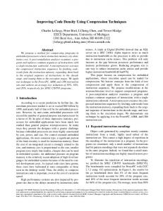
3.2.4 Automatic Target Recognition RTR is used within an automatic target recognition (ATR) application developed at UCLA to reduce the hardware resources required by a computationally demanding template-matching problem [80, 28]. The algorithm in this system is based on a correlation between incoming grey-scale synthetic aperture radar (SAR) image data and a set of binary target templates. This system exploits the advantages of FPGAs by specializing a unique correlation circuit to each of the target templates. The sparseness of the binary target templates used in this system signi cantly reduces the hardware resources required to complete the correlation. A hard-wired correlation circuit designed for a sparse template, for example, requires far fewer resources than a general-purpose correlation circuit designed to correlate an image against any template. To further improve the e�ciency of the computation, target templates with similar spatial arrangements are merged into a single custom circuit. As shown in Figure 3.9, merging of common templates allows the sharing of common resources for more than one correlation computation. The computational requirements of this system are intensi ed by the need to correlate each image against an extremely large set of target templates. Computing the correlation against all templates in parallel is not possible within a reasonable amount of hardware. Instead, the templates are divided into smaller, more manageable partitions. The correlation of the templates within each partition must be computed sequentially on the hardware resources. Because the hardware resources must support the correlation of any template in the template set, the special-purpose correlation circuits cannot be used with static hardware. To preserve the e�ciency of the special-purpose hardware, the FPGA resources are recon gured at run-time with the appropriate template-speci c correlation circuits. Template-speci c correlation circuits are recon gured onto the 30
Image Scan Lines
Template #1
Template #2
Figure 3.9: Merging of Similar Templates (adapted from [80] and used by permission). limited FPGA resources until all template correlations are complete. The run-time recon guration of template-speci c correlation circuits allows the use of extremely specialized and e�cient template correlation circuits without requiring enough hardware to complete all operations in parallel.
3.2.5 Stereo Vision A stereo vision algorithm was mapped to the DEC PeRLe-1 using runtime recon guration [35]. This circuit is based on a recursive software algorithm requiring a tremendous amount of computation [81]. The hardware implementation of this algorithm is divided into three distinct stages: data acquisition, correlation, and maximum detection. The data acquisition stage receives the input from the external source and stores the data into the system memories. The correlation stage performs a windowed correlation between two images at all o�sets and with multiple depth levels at each o�set. The last stage scales the correlated data using division and determines the maximum correlation at each o�set using a pipelined maximum detection circuit. Each stage of the computation requires all the data from the previous stage before proceeding. This requirement prevents the simultaneous execution of 31
all three stages. RTR is used to recon gure the hardware resources with circuits specialized to each of the three stages. The intermediate results produced and consumed by the circuit partitions are bu�ered on the host and transferred over the high-speed Turbo Channel I/O interface. Notwithstanding the need to recon gure FPGA resources at run-time, this system improves performance by a factor of thirty over four dedicated DSPs and a factor of 180 over a SPARC Station II.
3.2.6 Dynamic Instruction Set Computer (DISC) A simple programmable processor was created by the author to support the run-time recon guration of special-purpose computing structures. This system, called the Dynamic Instruction Set Computer (DISC) [82], allows a user program to determine the sequencing of the custom \instruction" units. The run-time recon guration of custom instructions allows a small array of FPGA resources to implement large, special-purpose algorithms. The details of this system will be described in Chapter 6 and Appendix C. Several image processing routines exploiting RTR were implemented on this architecture. An object thinning application, for example, demonstrated performance improvements over a software program by implementing computationally intensive operations in custom hardware [83]. This algorithm was partitioned into the following stages: input ltering, histogram generation, peak-detection, thresholding, and iterative thinning. Each of these stages were executed sequentially using a combination of custom, deeply pipelined circuits and general-purpose programmable functional units. The run-time recon guration of these circuits allowed the computation of this complex algorithm using a very modest array of FPGA resources.
3.3 Con guration Overhead Although run-time recon guration provides opportunities for circuit specialization not available in static systems, additional time is required during a computation for circuit recon guration. Unlike static specialization techniques,
32
which recon gure circuit resources o�-line or before a computation, run-time specialization techniques require recon guration to occur on-line or during the computation. Because circuit recon guration occurs during a computation, the recon guration time becomes a critical parameter of any RTR system | overall performance is directly a�ected by circuit recon guration time. The time to recon gure most of today's FPGA devices is on the order of milliseconds. Such a long time is several orders of magnitude longer than the time required to complete an individual operation. As such, the use of recon guration must be used carefully and sparingly. Careless use of recon guration can easily mitigate any advantages obtained by greater levels of specialization. Most applications reduce the e�ects of recon guration time by executing for long periods of time between recon guration. The stereo vision application, for example, is involved in actual computation over ve times as long as the associated recon guration time. The use of run-time circuit recon guration involves a trade-o� between the improvements in e�ciency due to run-time circuit specialization and the addition of con guration time. RTR will be used only if the advantages of run-time circuit specialization outweigh the disadvantages of con guration time. The following chapter will describe the method introduced in this dissertation of balancing the advantages of run-time circuit specialization with the disadvantages of con guration time.
33
Chapter 4
ANALYSIS OF RUN-TIME RECONFIGURED SYSTEMS In many cases, run-time recon guration allows a CCM system to exploit greater levels of specialization than possible with statically con gured systems. The advantages of these specialization techniques include the reduction of both the circuit area and the execution time required to complete a computation. However, these advantages must be balanced against the added time required for circuit con guration. Fortunately, the advantages of RTR and its associated costs (i.e. added con guration time) can be measured and allow quantitative analysis to guide its use. This chapter will introduce and de ne a new metric, termed functional density, that balances the reduction in circuit area obtained through RTR against its associated con guration time. Introduced in Section 4.1, this metric is based on the area-time costs required to complete a computation. Section 4.2 will augment the functional density metric for run-time recon gured systems by including the cost of circuit recon guration. Measuring functional density for run-time recon gured systems facilitates the comparison of run-time recon gured applications against conventional static approaches. Section 4.3 will describe the various ways the functional density metric can be used to evaluate run-time recon gured systems. The functional density metric is an important contribution of this work and will be used to evaluate several RTR applications in Chapter 5, the DISC system in Chapter 6, and several con guration improvement techniques in Chapter 7.
4.1 Functional Density Benchmarks used for most general-purpose computers are based on the speed or response time of a computation. The shorter the response time or latency of a computation, the more desirable the computer architecture. Most performance 34
metrics for general-purpose computers re ect this emphasis by specifying performance as the inverse of the execution time required to complete a computation [84]: 1 Performance (latency) = ; or; Execution Time
P = T1 : (4.1) Architectural enhancements strive to increase this measurement of performance by reducing the execution time or latency of a computation. Another common measure of performance is the throughput of a computation. Unlike the response time, which measures the absolute time to complete a given computation, throughput measures the rate of computation. Throughput is frequently measured by dividing the number of operations (n) by the time required to complete those computations (Tn): Performance (throughput) = Number of Operations ; or, Fixed Time P = Tn : (4.2) n Throughput is often more important in real-time computing environments that must sustain a minimum rate of computation. Examples of important throughput measurements include instructions per second within general-purpose processors, samples per second in a discrete-time signal processing environment, polygons per second in a 3-D graphics application, and frames per second within a video processing environment. Performance enhancing architectural techniques within these systems strive to increase the rate of computation.
Cost-Sensitive Benchmarks In most cases, performance enhancements are not available without cost. Most computing environments are cost-sensitive and must balance improvements in performance with any associated costs. Cost-performance metrics are frequently used to measure this trade-o�. Cost-performance metrics are usually calculated by dividing the performance of a computation by some measurable cost. The cost 35
associated with improved performance can be measured in many ways and often depends upon the speci c constraints of the system. For example, cost can be measured as a monetary value (i.e. dollars), power (watts), circuit area (um , � , etc.), or design time. Several metrics have been proposed to balance performance with cost. Such cost-performance metrics might include MIPS/watt, MIPS/um , and MIPS/dollar. Although several metrics are available for measuring the cost of a computation on a CCM platform, the most straightforward cost measurement is the amount of logic resources required to complete the computation. For FPGA based systems, the logic resource cost can be measured in terms of FPGA speci c logic element count (i.e. CLBs, cells, PFUs, etc.) or by the physical hardware area used by the computation (um , � , etc.). This logic resource or physical area cost will be generalized simply as the area (A) required by a computation. Using circuit area as its cost, the cost-performance of a CCM application is simply the performance of the application divided by its area, or, 1 CCM Cost-Performance = Performance = : Cost (Execution Time)(Circuit Area) This measurement provides the performance of unit-area logic resources or the \density" of computation among FPGA resources. This cost-sensitive metric is termed functional density (D) and is measured as the inverse area-time product as follows: 1 ; or, D = AT (4.3) n : = AT (4.4) 2
2
2
2
2
n
This metric is similar to the area-time cost metric commonly used to evaluate the e�ciency of VLSI circuits [85, 86]. Cost-sensitive metrics such as functional density are used to evaluate the cost-e�ectiveness of improvements or modi cations to existing architectures [87]. Such an analysis involves a cost-performance comparison between two architectures | one existing \base" architecture and another with some proposed architectural improvement. Although an architectural enhancement will undoubtedly improve performance, this type of analysis balances the increased performance against its 36
associated costs. Only those improvements that improve the cost-e�ectiveness of a computation are justi ed. This budget constrained analysis has been used to investigate the cost-e�ectiveness of increasing the width of a processor datapath [88]. Within a cost-sensitive analysis of RTR systems, functional density will be used to evaluate the e�ectiveness of a given run-time specialization technique. Speci cally, the functional density of a run-time recon gured circuit will be compared against that of a static, non-con gured circuit. If the use of a run-time specialization technique provides more functional density, it will improve the overall cost-e�ectiveness of the computation. The improvement in functional density of a circuit employing run-time recon guration is evaluated by measuring the normalized di�erence in functional density between the run-time recon gured system (Drtr ) and the static alternative (Ds) as follows, I = �DD = DrtrD? Ds = DDrtr ? 1: (4.5) s s s The improvement, I , can be measured as a \percentage" by multiplying by 100. When the functional density of the run-time recon gured system is greater than that of the static system (i.e. Drtr > Ds), the improvement, I , is positive and the use of run-time recon guration is justi ed. If, however, the added overhead imposed by con guration reduces the functional density below that of the static circuit (i.e. Drtr < Ds), I will be negative and the use of run-time recon guration will be di�cult to justify.
4.2 Functional Density of Run-Time Recon gured Systems In order to compare the functional density of a run-time recon gured system against a static system, the functional density metric of Equation 4.3 must be augmented for run-time recon gured systems. A system exploiting run-time recon guration requires additional time, system support, and bandwidth. Although each of these issues are important costs of an RTR system, the functional density metric will include only the added time of circuit recon guration. Unlike traditional static circuit-specialization techniques, run-time circuit specialization requires additional time for circuit recon guration. Circuit execution must halt during recon guration since conventional FPGAs do not support 37
simultaneous recon guration and execution . Thus, the con guration of circuit resources decreases the performance of an application by adding con guration time to the total operation time of the system. The total operational time of run-time recon gured systems includes both the execution time (Te) and con guration time (Tc) as follows: T = T e + Tc : (4.6) 1
The con guration time, Tc, is a device speci c parameter that will be addressed in Chapter 7. The functional density of a run-time recon gured system (Drtr ) is obtained by substituting the execution time of Equation 4.6 into the functional density metric of Equation 4.3, Dr = A(T 1+ T ) : (4.7) e c It is clear from Equation 4.7 that con guration time reduces functional density | as circuit recon guration time increases, the functional density will decrease.
Con guration Ratio Although the absolute con guration time of a system (Tc) is an important parameter of RTR systems, the ratio between con guration time and execution time is often much more informative. This ratio, termed the con guration ratio (f ), is obtained by dividing the con guration time of an RTR system by its associated execution time, f = TTc : (4.8) e
This con guration ratio is an important parameter of run-time recon gured applications and will be used extensively in the analysis of the applications in Chapter 5. The total operation time of an RTR system can be expressed in terms of this con guration ratio,
T = Te (1 + f ) :
(4.9)
Some systems propose the con guration of circuit resources during circuit execution. This issue will be addressed in Chapter 7. 1
38
Substituting Equation 4.9 into the original functional density metric provides a functional density metric in terms of f : Dr = AT (11 + f ) : (4.10) e As suggested in Equation 4.10, long con guration times can be tolerated if followed by correspondingly longer execution time. Systems that operate on large data-sets or exhibit a coarse granularity of run-time recon guration (con gure infrequently between major computation steps) have been shown to tolerate the relatively long con guration times of today's devices [23]. In the limit, as Te � Tc (i.e. f ! 0), the overhead imposed by con guration is negligible. Such systems approach the maximum functional density available by a RTR system. This maximum value, Dmax, is calculated by ignoring the e�ects of con guration time as follows: 1 : Dmax = flim D = (4.11) r ! ATe The functional density of Equation 4.10 can be represented in terms of Dmax by replacing the 1=ATe term with Dmax , (4.12) Dr = (1D+maxf ) : Clearly, the functional density of a RTR system will continually degrade as the con guration ratio f increases. This degradation of the functional density from the maximum value, Dmax , is plotted as a function of the con guration ratio f in Figure 4.1. Within Figure 4.1 there are two identi able regions. The functional density at the left-most area of the graph is near-maximum. This occurs when the con guration time is signi cantly smaller than the execution time and where changes in f have little e�ect on functional density. Within the right-most region, the con guration time dominates the total operation time. The functional density diverges from Dmax and changes in f have signi cant impact on the overall functional density. Any improvements in con guration time will signi cantly increase the functional density. Although there is no clear separation between the two regions, the functional density will reach 95% of Dmax when f falls below .05 (10? : ). At 95% of Dmax, f is less than .05 indicating that the execution time is at least twenty times the con guration time. 0
13
39
0
Functional Density, D/Dmax
10
−1
10
Functional Density Maximum Functional Density −2
10
−3
10
−2
10
−1
0
10 10 f, Configuration Time / Execution Time
Figure 4.1: Degradation of
D Dmax
1
10
2
10
vs. f .
4.3 Architectural Analysis The bene ts and limitations of run-time recon gured applications can be analyzed by measuring the functional density for both statically con gured and run-time recon gured systems. This section will describe an approach for analyzing run-time recon gured applications using the functional density metric. This analysis can be used to determine the appropriateness of RTR, justify RTR over conventional implementation approaches, and identify the overhead imposed by circuit con guration for any given application considering the use of RTR. It is important to reiterate that any analysis of run-time recon gured applications must include some comparison against a static alternative. Run-time recon gured applications are sometimes published without a comparison against other conventional static approaches | this lack of comparison hides the advantages (or disadvantages) o�ered by RTR. Run-time recon guration will not become a common technique within CCM machines unless improvements over traditional 40
approaches can be shown. The approach for analyzing run-time recon gured applications within this thesis will be based on the comparison of a run-time recon gured implementation against a more conventional static alternative performing the same function on the same CCM platform.
4.3.1 Application-Speci c Circuit Parameters The rst step in the analysis of a run-time recon gured application is to obtain the application-speci c parameters needed to compute the functional density for both the run-time and static implementation approaches. These parameters include performance (Te or Tnn ), circuit area (A), and con guration time (Tc). Obtaining these values may require the complete design and timing analysis of each of the two circuit implementations. Alternatively, this may involve an estimation based on the known circuit parameters of sub-modules used within the design. In either case, the performance and area measurements of both implementation approaches form the basis of the analysis. In many cases, these application-speci c parameters depend on the size or scope of the computation. The execution time, for example, will often depend on the amount of data processed by the application (i.e. sample size, string length, etc.). Even the size of the circuit can depend upon the scope of the problem. The DNA sequencing circuit described in Section 3.2, for example, requires a distinct processing element for each character of the source sequence. In these cases, the overall functional density of the application will be a function of the size or scope of the problem. Before calculating the con guration overhead imposed by the RTR version of the application, it is helpful to understand the maximum bene ts available with RTR. Understanding the maximum bene ts of RTR provides an early indication of the appropriateness of RTR for a given application before the e�ects of con guration are considered. The maximum improvement, Imax, is de ned as the improvement o�ered by the maximum functional density, Dmax (see Equation 4.11), over the static approach as follows: Imax = DDmax ? 1: (4.13) s 41
Those RTR applications with a large potential improvement in functional density are likely good candidates for run-time recon guration.
4.3.2 Comparing Functional Density With suitable application-speci c circuit parameters available for both the static and RTR implementation approaches, the functional density of both systems can be compared. The run-time recon gured approach will be justi ed if it provides more functional density than the static alternative. The run-time recon gured version of the application improves the functional density when the reduction in circuit resources due to run-time specialization are more signi cant than the overhead imposed by circuit con guration. The conditions in which run-time recon guration improves functional density can be investigated by examining the relation Drtr > Ds. Representing Ar and Tr as the area and execution time of the run-time recon gured circuit, this relation can be reduced as follows:
Drtr � Ds; 1 Ar (Tr + Tc) � Ds; 1 � 1 � � 1 + Tc : (4.14) Ds Ar Tr Tr This relation can be simpli ed by substituting Dmax and f as follows: Dmax ? 1 � f: (4.15) Ds The left hand side of the relation is the maximum improvement possible with RTR (see Equation 4.13). Substituting Imax into Equation 4.15 produces the relation: Imax � f:
(4.16)
Equation 4.16 is an important result that describes the maximum allowable con guration ratio, f , of a given RTR system. This relation states that in order for a run-time recon gured system to provide more functional density than a static alternative, the con guration ratio must be less than the maximum potential improvement (Imax ) of the run-time recon gured system. 42
Intuitively, the relation of Equation 4.16 suggests that the greater the potential advantage of a run-time recon gured circuit, the less stringent the con guration overhead limitations. Those run-time recon gured circuits providing substantial improvements in e�ciency are less sensitive to con guration time than those providing only marginal potential improvements. Only those run-time specialization techniques that provide signi cant improvements in e�ciency justify RTR in light of the poor con guration performance of today's devices. This result also suggests that systems providing only modest improvements with RTR can still be justi ed so long as the con guration ratio is low.
Example Use of Functional Density To demonstrate the use of this analysis approach, consider a static circuit requiring circuit area a and time t to complete a given operation. Suppose a run-time recon gured circuit performs the same computation in half the area ( a ) and two-thirds the time ( t ). As summarized in Table 4.1, the maximum improvement of the RTR circuit is 2 (200%). Using Equation 4.16, this result suggests that the RTR circuit will provide greater functional density than the static circuit so long as f < 2, or as the con guration time is less than twice the execution time. 2
2 3
A T Dmax Imax Static a t at 0 a t RTR 2 at 1
2
2 3
3
Table 4.1: Example Circuit Parameters and Functional Density. To demonstrate the e�ects of con guration time on this example, the functional density of the run-time recon gured system can be represented in terms of its maximum functional density (Dmax) and the con guration ratio f as suggested in Equation 4.12. The functional density of this example is plotted as a function of f in Figure 4.2 along with the functional density of the static alternative and its maximum value, Dmax . With a very low con guration overhead (i.e. Tc � Te), the functional density of this example is near its maximum, Dmax. However, as the con guration 43
overhead increases the functional density decreases until it falls below the functional density of the static system. Consistent with the result obtained above, the point at which the two systems provide the same functional density occurs when f = 2 (10: ). As the con guration overhead increases beyond this break-even point, the functional density of the run-time recon gured system is less than that of the static circuit.
Functional Density, D/Dmax
3
0
10
Static Functional Density Functional Density Maximum Functional Density −3
10
−2
10
−1
0
10 10 f, Configuration Time / Execution Time
1
10
Figure 4.2: Example Functional Density Comparison. The analysis approach introduced in this chapter and demonstrated with this simple example can be used to evaluate the use of RTR within actual CCM applications. The following steps summarize the analysis of RTR systems: 1. Obtain the area and performance measurements of both the static and runtime recon gured systems, 2. Compute the maximum improvement (Imax ) of the run-time recon gured circuit using the circuit parameters obtained above, 3. Determine the maximum con guration ratio, fmax , allowable for this system based on Imax , 44
4. Determine the con guration time, Tc, of the intended FPGA, and 5. Compute f using Tc and Te and determine if f < Imax . If f < Imax for the problem sizes of interest, RTR can be justi ed, otherwise, RTR is not justi ed. Even though the use of RTR may be justi ed using the functional density measurment, other factors must be considered before employing RTR within a system. The added design time, con guration bandwidth, and support circuitry needed to implement RTR may mitigate its use within an actual system. This analysis will focus primarily on the improvements in functional density provided by RTR systems. The analysis approach listed above will be used to demonstrate the advantages of several RTR applications in Chapter 5.
45
Chapter 5
APPLICATIONS This chapter will demonstrate the analysis technique presented in the previous chapter by measuring the functional density of several run-time recon gured applications. Each application has been mapped to existing FPGA technology and demonstrates improvements in functional density by exploiting RTR. The applications used in this study include the following:
� � � �
Run-Time Recon gured Neural Network, Partially Run-Time Recon gured Neural Network, Template Matching Circuit, and DNA Sequencing Circuit.
For each of these applications, two implementation approaches will be presented | a static non-con gured circuit and the run-time recon gured circuit. The functional density will be calculated for each approach to determine if and when the use of run-time recon guration improves the functional density of the application. Calculating the functional density for each application will require the circuit parameters of both logic resource utilization and execution time. In addition, the con guration time will be required for the run-time recon gured circuit. In most cases, the calculation of these parameters will depend on the size of the desired computation (i.e. network size, image size, or DNA sequence length). The analysis of the applications within this chapter will involve the modeling and evaluation of functional density based on these system parameters.
5.1 Run-Time Recon gured Arti cial Neural-Network The run-time recon gured neural network (RRANN) was one of the rst applications to demonstrate improvements in circuit density by exploiting run-time circuit recon guration [89]. Introduced earlier in Chapter 3, this neuralnetwork application implements the popular backpropagation learning algorithm 46
using custom hardware. RTR is used within this application to recon gure the system's hardware neurons between special-purpose neural processors customized for each of the three backpropagation stages (see Figure 3.2). The reduction in size associated with this run-time specialization allows six times as many special-purpose neurons to operate within the same amount of hardware as a static, general-purpose neuron. The RRANN project demonstrates this increase in neuron density by developing and comparing a static non-con gured neural network against a run-time recon gured neural network. Both approaches were designed and tested on the same CCM platform to provide a fair comparison of the FPGA resource required by each approach. In addition, the negative e�ects of con guration time were considered when comparing the two approaches. This discussion will extend the analysis rst presented with RRANN by applying the analysis approach described in the previous chapter. Based on the functional density metric, this analysis will identify if and when RTR is justi ed for this neural-network architecture. The analysis of the RRANN architecture will also be used to investigate the bene ts of RTR for the \Rock vs. Mine" target application described in [90]. This network application requires three neuron layers with 60 neurons in the rst layer, 36 neurons in the second layer, and two neurons in the last layer.
5.1.1 RRANN System Architecture Before identifying the application-speci c parameters necessary for computing the functional density of RRANN, it is necessary to review the system architecture of RRANN and describe how the system scales with additional neurons. The RRANN architecture was designed to scale with network size by limiting the growth of the hardware, interconnection and execution time of the network to O(n). The size of the network is an important system parameter since it a�ects the hardware resources, execution time, and ultimately the functional density of the computation. The RRANN architecture consists of a global controller and an array of FPGA based neural-processors. As shown in Figure 5.1, the global controller and neural processors communicate over a series of global system busses. Neurons 47
within the network are interconnected in a time-multiplexed scheme in order to limit growth of both the interconnect and hardware required by the network. Using this time-multiplexed interconnection scheme limits the growth of the execution time and hardware area to O(n), where n is the number of neurons per layer of the network. Adding neurons to the network will lengthen the execution time and require more hardware resources. Data/Control Bus
PC Host
Global Controller
Neural Processor
Neural Processor
FPGA
FPGA
FPGA
RAM
RAM
RAM
Broadcast Bus Error Bus
Figure 5.1: System Architecture of RRANN. Because both the area and execution time of RRANN are determined by the number of neurons within the network, the functional density of RRANN will also depend on the size of the network. The following sections will describe the application-dependent circuit parameters needed to calculate the functional density and specify each parameter in terms of the neurons required by the largest layer within the system. These network-speci c parameters will also be applied to the 60 neuron \Rock vs. Mine" application mentioned above.
5.1.2 Performance The training performance of this network is based on the throughput measurement of weight-updates per second, or WUPS. This performance measurement is made by dividing the number of weighted-connections (synapses) within the network by the time required to update each weight (i.e. the time to complete 48
one complete iteration of the training algorithm): (5.1) P (WUPS) = CT ((nn)) : Each of these parameters is a function of the number of neurons within the system.
Weighted Connections The number of weighted connections within a neural network is determined by the number of layers in the network (l) and the number of nodes within each layer (Nodes[x]) as follows:
C=
l?1 X x=1
Nodes[x] � Nodes[x + 1]:
(5.2)
For the purpose of simplifying the analysis, the following assumptions can be made:
� The network consists of four layers (l = 4), � All layers contain the same number of nodes (i.e. Nodes[i] = C for all i). These assumptions reduce the calculation of the connection count to:
C (n) = 3n ;
(5.3)
2
where n is the number of neurons within the largest layer. The network with 60 neurons per layer, for example, contains 10,800 weighted connections (synapses).
Execution Time The execution time (Te) required to complete the computation of an entire iteration of the algorithm is the same for both the static and RTR versions. The execution time is obtained by multiplying the clock cycle count for a single iteration of the algorithm by the clock frequency. The clock cycle count is determined by the number of non-output neurons in the network (N ) and the number of layers (l) as follows (adapted from Equation 7 of [23] ): 1
cycle count =
l?1 X x=1
!
Nodes[x] � 148 + (l ? 1) � 13 + 282:
(5.4)
A more accurate equation described in [91] considers the quantization errors associated with larger networks. The added execution time required to address the quantization error is negligible and does not e�ect the results of this analysis. 1
49
Multiplying the cycle count by the clock rate and applying the assumptions stated above (l = 4, and Nodes[x] = n) reduces the execution time of one iteration of this algorithm to:
Te(n) = (444n + 321)tclk:
(5.5)
With a clock cycle of 14 MHz (tclk = 71 ns), the network of 60 neurons per layer requires 1.93 ms to execute the algorithm for one complete iteration. The composite performance of the RRANN network is computed by dividing the connection count by the execution time: 3n P (n) = CT ((nn)) = (444n + (5.6) 321)tclk : Training the 10,800 connections of the 60 neurons per layer network, for example, requires 1.93 ms for a composite performance of 5.61 �10 WUPS. For the run-time recon gured network, the execution time for a single iteration of the algorithm will require three con guration steps. During circuit recon guration the network is idle and no computation takes place. To account for recon guration, the total execution time for the RTR circuit must add the time required for these three recon guration steps. This added con guration time reduces the performance of the network as follows: 3n (5.7) P (n) = T (Cn)(n+) T = (444n + 321) tclk + Tc : e C 2
6
2
5.1.3 Area Cost To complete the computation of functional density for RRANN, the area costs of each approach must be known. The area of the circuit, like its execution time, depends upon the number of neurons within the system. The total area consumed by a network includes the area used by the global controller (agc) and the area consumed by each neuron (an) within the network,
A = agc + nan :
(5.8)
Within the original analysis of RRANN, the area of the circuit was measured in terms of the number of Xilinx 3090 FPGAs. This analysis will measure 50
area in terms of the number of Xilinx 3000 series con gurable logic blocks (CLBs) used by the design. Using the CLB count instead of the FPGA count for the area measurement o�ers several advantages. First, measuring circuit area in terms of the FPGA count introduces quantization error. Unused resources within FPGAs are unnecessarily attributed to the computation. Second, specifying a particular FPGA for the area measurement limits the analysis to the speci c FPGA device. Measuring area in terms of CLBs allows application of the analysis to other FPGAs within the same FPGA family. The CLB resources required by the global controller and the various neural processors are listed in Table 5.1. Global Controller Neural Processors CLBs CLBs Neurons CLBs/Neuron y Static System 150 235 1 235 Feedforward 97 260 6 43.3 Backpropagation 62 253 6 42.2 Update 98 224 6 37.3 y
Estimated
Table 5.1: RRANN Circuit Parameters. Assuming an estimated 150 CLBs for the global controller of the static system, the total hardware area for the global controller and the neural processors is calculated as follows:
Astatic (n) = 150 + 235n:
(5.9)
Measuring area for the run-time recon gured case is slightly more complicated. The run-time recon gured approach uses three di�erent neural processors | each with di�erent hardware requirements. The hardware required for a neural processor varies from 37 CLBs for the update processor to 43 CLBs for the feedforward processor. At run-time, the resource utilization of the system will change as the system is con gured between the various phases of the algorithm. To account for these di�erences in area, the area of the largest neural processor will be used. The area of the largest processor is used because the resources made available by neural processors with fewer resources are idle and cannot be used for other 51
purposes. The update phase has the largest global controller at 98 CLBs and the feedforward phase has the largest neural processor at 43.3 CLBs. The total area of the run-time recon gured system is,
Artr = 98 + 43:3n: (5.10) The savings in hardware area due to run-time recon guration reduces the CLB requirements for the n = 60 network from 14,250 to 2,696 CLBs.
5.1.4 Functional Density The functional density of these two systems can be calculated by combining the performance and area cost measurements obtained above. Using the performance measurement of Equation 5.6 and the area cost of Equation 5.9, the functional density of the static system is determined as follows: 3n Dstatic (n) = (150 + 235n)(444 (5.11) n + 321)tclk : The functional density of the run-time recon gured system is obtained by combining the performance measurement of Equation 5.7 with the more e�cient area measurements of Equation 5.10 as follows: 3n Drtr (n) = (98 + 43:3n)[(444 (5.12) n + 321)tclk + Tc] : The functional density of a static network with 60 neurons per layer achieves 394 weight-updates per second per CLB (WUPS per CLB). The maximum functional density (Dmax ) is found by ignoring the e�ects of con guration time (i.e. Tc = 0). The maximum functional density of the n = 60 network achieves a value of 2079 WUPS per CLB. Before investigating the e�ects of con guration overhead on the functional density of the run-time recon gured circuit, it is important to identify the maximum bene ts available with RTR. The maximum improvement available with RTR (Imax ) is obtained by substituting the functional density results above into the maximum improvement of Equation 4.5: Imax (n) = DDmax ((nn)) ? 1; static (5.13) = 150 + 235n ? 1: 98 + 43:3n 2
2
52
The maximum improvement of the run-time recon gured n = 60 network is 4.28 or a 428% improvement over its statically con gured counterpart. The circuit parameters and maximum functional density of both the static and RTR implementation approaches for the 60 neuron network are listed in Table 5.2. Static RTR Neurons/Layer (n) 60 Connections 10800 Te (ms) 1.93 P (WUPS) 5.61�10 A (CLBs) 14250 2696 WUPS Dmax ( CLB ) 394 2079 Imax 0 4.28 6
Table 5.2: Circuit Parameters for a 60 Neuron Network. This maximum improvement of 4.28 suggests that RRANN has the potential to o�er signi cant improvements over its static alternative. Such a large improvement due to run-time recon guration indicates that this application is an excellent candidate for RTR. This result indicates that each iteration of the 60 neurons per layer RRANN architecture can tolerate a con guration time of up to four times the execution time and still provide greater functional density than the static alternative. For every 1.93 ms of execution time required for an iteration of the backpropagation algorithm, up to 8.26 ms of additional time can be spent con guring the FPGAs and still provide more functional density than the static alternative.
5.1.5 Con guration Overhead Although early evaluations of this application indicate that RTR provides signi cant improvements, the actual con guration overhead must be considered. The con guration rate of RRANN is limited by the con guration time of the associated Xilinx 3090 FPGAs. Fortunately, the FPGA board used by RRANN allows the parallel con guration of all FPGAs in the system. This allows the 53
con guration time of the system to remain constant for networks of any size . A con guration step is required to con gure the hardware resources between each of the three phases of the backpropagation algorithm. Using the serial slave mode, a single FPGA requires 6.4 ms to con gure the 64,160 con guration bits over the 10 MHz serial interface. Three such recon guration steps require a total 19.2 ms. Unfortunately, this recon guration time is larger than the maximum allowable con guration time. A con guration time of 19.2 ms is almost ten times the execution time for a con guration ratio of f = 9:9. Substituting the con guration time into the functional density of Equation 5.12 reduces the functional density from its maximum value of 2696 WUPS/CLB to 189 WUPS/CLB. Due to the excessive con guration overhead, the functional density of the run-time recon gured approach is 52% lower than that of the static approach (see Table 5.3). 2
Tc (ms) f Drtr I
19.8 9.95 189 -.52
Table 5.3: Con guration Overhead of a 60 Neuron Network. Although the con guration time for the network of 60 neurons per layer reduces the functional density of the RTR approach below the functional density of the static version, the con guration overhead can be reduced by increasing the size of the network. Since the con guration time is constant while the execution time increases with network size, the con guration overhead will decrease as the size of the network increases. This reduction in the con guration overhead is demonstrated by dividing the xed con guration time of 19.2 ms by the execution time of Equation 5.5: f = TTc ; e = (444n19+:2ms 321)tclk ; This is true for networks that t within a single board. If multiple boards are required, the con guration bandwidth will be limited by the system bus interface. 2
54
269 � 10 : = 444 (5.14) n + 321 This reduction in con guration ratio, f , is shown in Figure 5.2 by plotting f as a function of network size, n. Clearly, the con guration ratio declines as the network size increases. 3
2
1
10
Maximum Improvement, Imax
Configuration Ratio, f 66 Neurons
Configuration Overhead (Tc/Te)
10
0
10
0
50
100
150
200 250 300 Neurons per Layer
350
400
450
500
Figure 5.2: Con guration Overhead of RRANN. Plotted along with the con guration ratio is the maximum improvement, Imax , of Equation 5.13. As described in Chapter 4, RTR is justi ed when the con guration ratio is less than maximum improvement, Imax . As seen in Figure 5.2, networks of su�cient size drop below Imax and justify RTR. Although RTR is not justi ed for the 60 neuron network, networks of su�cient size execute long enough to overcome the overhead imposed by con guration time. The break-even point at which the functional density of the static approach equals that of the RTR approach can be found by setting the functional 55
density of the run-time recon gured circuit equal to the functional density of the static circuit and solving for n:
Drtr = Dstatic ; 3n 3n = (98 + 43:3n)[(444n + 321)tclk + 19:2ms)] (150 + 235n)(444n + 321)tclk ; n = 139: (5.15) 2
2
The recon guration overhead of the run-time recon gured circuit limits the bene t of RTR to networks with at least 139 neurons per layer. For networks larger than 139 neurons per layer, RTR will provide more functional density than the static approach. Figure 5.3 summarizes the e�ects of network size, n, on the overall functional density of the RRANN architecture. Plotted along with the functional density of the RTR approach is the functional density of the static, non-con gured circuit and the maximum functional density of the RTR approach (i.e. Tc = 0). Several important facts are con rmed from this plot. First, the use of RTR reduces the functional density of the system at n = 60. Second, the functional density of the RTR approach increases with network size and equals the static approach at n = 139. Third, for network sizes greater than 139 neurons per layer, the functional density continues to improve and approaches the maximum functional density Dmax for a 400% improvement over the static approach. The use of run-time recon guration within the RRANN application signi cantly reduces the hardware requirements of neural processors within the backpropagation algorithm. RRANN demonstrates an increase of 500% in neuron density by exploiting run-time recon guration. However, the signi cant con guration overhead required by RRANN limits the use of RTR to networks with at least 139 neurons. This requirement suggests that RTR is not appropriate for neuralnetworks such as the \Rock vs. Mine" with only 60 neurons. Unless con guration time is reduced, RTR cannot be justi ed for most neural-network applications.
5.2 Partially Run-Time Recon gured Arti cial Neural-Network Although the RRANN architecture demonstrates a signi cant reduction in hardware density through run-time recon guration, RRANN does not achieve 56
2000
Static Functional Density
1500
RTR Functional Density Maximum Functional Density 1000
60 Neurons
Functional Density, D (Weight−Updates/CLB−sec)
2500
500
0 0
50
100
150
200 250 300 Neurons per Layer
350
400
450
500
Figure 5.3: Functional Density of RRANN. signi cant improvements in functional density unless a large sized neural network is used. Failure to improve the functional density is due to the extreme sensitivity of the RRANN architecture to con guration time. To address this issue, a second RRANN architecture (RRANN-II) was developed [70]. RRANN-II was designed to exploit the reduced con guration time of partial recon gurability and the improved con guration bandwidth available with the National Semiconductor CLAy FPGA [78]. Other than a few architectural modi cations, RRANN-II was designed to solve the same algorithm used in the original RRANN architecture. The backpropagation algorithm is partitioned into the same three sequentially executing phases: feedforward, backpropagation, and update. In addition, the same scalable system architecture depicted in Figure 5.1 is used by RRANN-II. The major di�erence between RRANN-II and its predecessor is its use of the partially con gurable CLAy FPGA. A development board based on the CLAy FPGA was modi ed to 57
implement the RRANN architecture described in Figure 5.1. Because the algorithm and implementation approach of RRANN-II is so similar to the original RRANN architecture, the analysis of RRANN-II will be very similar to the analysis of the original RRANN architecture. The functional density metric will be used to analyze the viability of the 60 neuron per layer \Rock vs. Mine" application described earlier. However, the RRANN-II analysis presented in this section will focus on the bene ts of partial con guration. Two variations of the run-time recon gured circuit will be compared against the static, non-con gured baseline architecture. The rst is a globally con gured circuit that recon gures all circuit resources between algorithm steps. This is the traditional global RTR approach used in the original RRANN architecture. The second RTR variation is the partially con gured circuit that con gures only changes between the algorithmic steps. Such a comparison will identify the advantages provided by partial con guration.
5.2.1 Partial Con guration Partial con guration, available within several FPGA families [92, 78, 93], allows con guration of a subset of logic resources within an FPGA. Instead of requiring the user to con gure all FPGA resources, small pieces within the FPGA can be con gured as needed. Within run-time recon gured systems, this feature provides two important advantages. First, the ability to con gure a subset of the device reduces the amount of con guration data required at each recon guration step. Such a reduction in con guration data directly reduces the e�ective con guration time. Second, the ability to preserve circuitry of some FPGA resources during con guration allows crucial state information to be saved within the device during con guration. This avoids the overhead of loading and storing the system state between the circuit con guration steps. The RRANN-II architecture attempts to extend the advantages of RTR by exploiting both of these advantages. To exploit the advantages of partial recon guration, RRANN-II identi es the similarities between each of the three specialpurpose neural processors. Each special-purpose processor is designed to share as much hardware as possible to limit the amount of con guration data required to 58
convert one processor into another [94]. In order to design a system that is partially con gurable, the RRANNII project required considerable hand-layout and manual design. The rst design step of this project was the manual placement of common circuit functions used by all three neural processors. These circuits, shared by all processors, remain static throughout the computation and do not require circuit recon guration. The common circuit functions within RRANN-II include the address generation units, accumulator registers, over ow/under ow detectors, and basic I/O control. After mapping these shared functions, circuits unique to each neural processor were identi ed and designed. The circuits unique to each neural processor include the global neural processor control, the multiplier, and several xed constants. These circuit \modi cations" were carefully designed and mapped to interact properly with the static logic that remains on the FPGA at all times. The recon guration time is reduced with this approach by limiting circuit recon guration to these circuit modi cations. The hand-layout of this circuit produced a very e�cient and highly optimized design. Each of the system circuits operate at 20 MHz and achieve unusually high utilization of the ne-grain FPGA resources. The static, noncon gured neural processor contains three neurons within a single FPGA. The run-time recon gured neural processor, which o�ers the advantages of increased specialization, increases the neuron density to nine neurons per FPGA.
5.2.2 Performance Like RRANN, the performance of RRANN-II is measured in terms of weight-updates per second, or WUPS as speci ed by Equation 5.1. The connection count for RRANN-II, however, is slightly di�erent than that of the connection count used by RRANN. RRANN-II adds bias-nodes to increase the networks ability to learn. The addition of the bias node is indicated by the \+1" term in the connection count,
C=
l?1 X x=1
(Nodes[x ? 1] + 1) � Nodes[x]:
59
(5.16)
By making the same assumptions that were made with RRANN (i.e. 4 layers and n neurons per layer), the connection count reduces to:
C = 3n(n + 1):
(5.17)
This modi ed equation for the connection count increases the number of synapses within the 60 neuron network to 10,980. The cycle count required to execute the three phases of the backpropagation is also speci ed in terms of the network size. Adapted from Equation 6.9 of [70], the cycle count for RRANN-II is speci ed as follows: cycle count = 113n + 184n(l ? 2) + 170(l ? 1) + 347:
(5.18)
The total execution time is calculated by applying the same assumptions (l = 4 and n = Nodes[x]) and multiplying by the clock period:
Te(n) = (481n + 857)tclk:
(5.19)
The extra cycles required by RRANN-II are due to the addition of the bias nodes and deeper pipelining within the circuit. The deep pipeline allows the circuit to operate at 20 MHz (tclk = 50 ns) and reduces the total execution time for the 60 neurons per layer network to 1.49 ms. The composite performance of RRANN-II system is found by dividing the connection count by the execution time, 1) : P (n) = (4813nn(+n + (5.20) 857)tclk The performance of a static version of this training algorithm for the 60 neuron network is 7.39 �10 WUPS. 6
5.2.3 Area Cost To compute the functional density of RRANN-II, the area of each circuit must be known. The use of the CLAy FPGA for RRANN-II requires the devicespeci c measure of area in terms of CLAy cells. The total area for the computation includes the area of the global controller and the neural processors as suggested in 60
Global Controller Neural Processors cells Neurons cells cells/Neuron Static System 844 3 2497 832 Feedforward 844 9 2207 245 Backpropagation 844 9 2712 301 Update 844 9 2376 264 Table 5.4: RRANN Circuit Parameters. Equation 5.8. The area requirements for the global controller and neural processors are listed in Table 5.4 in terms of CLAy cells. The global controller for both the static and run-time recon gured system is the same and consumes 844 cells of the global controller FPGA. The neural processors, however, di�er in size. Each static, non-con gured neural processor consumes 832 cells with three such processors operating within a CLAy31 FPGA. The total area consumed by the static circuit is
A(n) = 844 + 832n:
(5.21)
Run-time specialization of the neural processors reduces the amount of hardware required to complete the algorithm. Nine specialized neural processors, for example, can t within the same CLAy31 FPGA. Although nine neural processors t within the FPGA, the actual cell count for each neural processor di�ers. The neural processor with the largest cell count (backpropagation) will be used since the free hardware resources of the other stages cannot be used productively. The total area consumed by the run-time recon gured circuit is
A(n) = 844 + 301n:
(5.22)
For the 60 neuron network, run-time recon guration reduces the hardware requirements from 50,764 cells to only 18,904 cells.
5.2.4 Functional Density The functional density metric for both the static and run-time recon gured circuits can be computed by substituting the performance and area cost 61
metrics obtained above. Functional density for RRANN-II will be measured in terms of weight-updates per second per cell, or WUPS per cell. The functional density of the static circuit is obtained by dividing the performance measure of Equation 5.20 by the area cost of Equation 5.21, (n + 1) (5.23) Dstatic (n) = (844 + 8323nn)(481 n + 857)tclk : The functional density of the 60 neuron network operating on the static, noncon gured system is 146 WUPS per cell. The functional density metric of the run-time recon gured system is obtained by augmenting the same performance measure of Equation 5.20 with the recon guration time and reduced area. Using the area cost of the more e�cient run-time recon gured circuit from Equation 5.22, the functional density reduces to, 3n(n + 1) Drtr (n) = (844 + 301n)[(481 (5.24) n + 857)tclk + Tc] : With zero con guration overhead (i.e. Tc = 0), the maximum functional density of a run-time recon gured 60 neuron network is 391 WUPS/cell. Without knowing the overhead imposed by circuit recon guration, the maximum improvement of the run-time recon gured circuit can be found. The maximum improvement o�ered by RTR is found by substituting the functional density of both systems into the maximum improvement of Equation 4.5, (844 + 833n) ? 1: Imax (n) = (844 (5.25) + 302n) The maximum improvement for the RTR approach of RRANN-II with n = 60 is 1.68 or 168%. With an execution time of 1.49 ms, the maximum allowable con guration time of the run-time recon gured system is 2.50 ms (see Equation 4.16). The circuit parameters of both the static and RTR implementation approaches are listed in Table 5.5.
5.2.5 Con guration Overhead Like its predecessor, the advantages o�ered by RTR within RRANN-II are limited by the circuit recon guration time. However, RRANN-II was designed 62
Static
RTR
Neurons/Layer (n) 60 Connections 10,930 Te (ms) 1.49 P (WUPS) 7.39�10 A (cells) 50,764 18,904 WUPS Dmax ( cell ) 146 391 Imax 0 1.68 6
Table 5.5: RRANN-II Circuit Parameters for a 60 Neuron Network. to reduce the con guration overhead by exploiting both the higher con guration bandwidth of the CLAy FPGA and the partial recon gurability of the device. RRANN-II will investigate the advantages of both global RTR and partial recon guration. This section will address the recon guration time of the global and partial run-time recon gured implementation approaches and identify the e�ects of these recon guration times on functional density. The recon guration time of RRANN-II is limited by the parallel recon guration of its neural processor FPGAs . Since a single CLAy31 FPGA requires .808 ms for complete recon guration, the three recon guration steps consume a total of 2.42 ms for a complete iteration of the training algorithm. The byte-wide con guration path of the CLAy device allows con guration to occur almost eight times faster than the con guration time of the original RRANN project. Fortunately, the con guration time of the globally con gured RRANNII approach is slightly lower than maximum allowable con guration time of 2.50 ms. This insures that the globally recon gured approach will provide more functional density than the non-con gured static alternative. When substituting the con guration time of 2.42 ms into Equation 5.24, a functional density of 148 WUPS per cell is achieved for a 1.4% improvement over the static alternative. 3
3 Like most FPGA based boards, the con guration of the board used for RRANN-II is actually limited by the host system bus. The RRANN-II analysis assumes con guration is limited by device con guration constraints and not the bus bandwidth limitations.
63
Partial Con guration As suggested earlier, one of the major purposes of the RRANN-II project is to reduce the excessive con guration time of RTR systems by partially recon guring circuit resources. By limiting con guration within an FPGA to circuit changes, the amount of data required for con guration can be signi cantly reduced. Reducing the con guration data directly reduces the time required for circuit recon guration. RRANN-II investigates the bene ts of this technique by recon guring only the changes needed to convert the neural processors from one phase to the next. For example, recon guring FPGA resources from a feedforward neural processor into a backpropagation neural processor is accomplished with only 4163 bytes | 48% fewer con guration bytes than needed by a full con guration step. The reduction in con guration data for each of the three neural processors is shown in Table 5.6. The total recon guration time of the partially recon gured system is reduced from 2.42 ms to 1.16 ms for a reduction in con guration time of 52%. Con guration
Bit-Stream Size (bytes) Complete FPGA 8078 Feed-Forward to Backpropagation 4163 Backpropagation to Update 4378 Update to Feed-Forward 2729
Time Reduction Total (�s) (ms) 807.8 0% 2.42 416.3 48.5% 473.8 45.8% 1.16 272.9 66.2%
Table 5.6: RRANN-II Partial Bit-Stream Sizes. Reducing the con guration time through partial con guration increases the functional density of the 60 neuron network. By applying the con guration time of 1.16 ms into Equation 5.24, the functional density of this partially recon gured system increases to 219 WUPS per cell. This represents a 50% improvement over the static implementation approach. The improvement in functional density for both the global and partially recon gured systems is listed in Table 5.7. Although both the global and partially con gured circuits improve functional density for the 60 neuron network, it is important to investigate the e�ect of network size on the functional density. As additional neurons are added to this 64
Global RTR Partial RTR Tc (ms) 2.42 1.16 f 1.62 .779 Drtr 148 219 I .014 .50 Table 5.7: Improvement in Functional Density of RRANN-II. system, the execution time will increase. With a constant con guration time, the con guration ratio will correspondingly decrease. Figure 5.4 plots this decrease in con guration ratio as a function of network size. Plotted along with the con guration ratio is the maximum improvement of the RRANN-II architecture. In those areas where the con guration ratio is less than Imax , RTR is justi ed. The lower recon guration time of the partially con gured system reduces this break-even point | this justi es smaller networks for the partially recon gured system. The break-even points of both systems can be evaluated by setting the functional density of the static circuit (Equation 5.23) equal to the functional density of the run-time recon gured circuit (Equation 5.23) and solving for n. Using a con guration time of 2.42 ms for the globally con gured circuit, the break-even point occurs at a network size of 58 neurons. For the partially con gured circuit (Tc = 1.16 ms), the break-even point is reduced to 28 neurons. Lowering the breakeven point allows smaller sized networks to bene t from run-time recon guration. The e�ects of network size on the functional density of all three approaches are summarized in Figure 5.5 by plotting the functional density of the static circuit with the functional density of the partially con gured circuit. In addition, the maximum functional density of the run-time recon gured circuit is shown for reference. Two important advantages of partial recon guration are demonstrated in this plot. First, a shorter con guration time within the partially recon gured system insures that its functional density is greater than that of its globally con gured counterpart. Second, and often more important, the break-even at which RTR is justi ed is much lower for partial recon guration than global recon guration. Although the maximum advantages of RTR within the RRANN-II 65
1
Maximum Improvement, Imax
0
10
60 Neurons
Configuration Overhead (Tc/Te)
10
Global Configuration Ratio, f
Partial Configuration Ratio, f
−1
10
0
50
100
150
200 250 300 Neurons per Layer
350
400
450
500
Figure 5.4: Con guration Overhead of RRANN-II. architecture are lower than that of its predecessor (i.e. RRANN), the shorter con guration time within RRANN-II and the ability to exploit partial recon guration allows smaller, more useful networks to enjoy the bene ts of RTR.
5.3 Template Matching Template matching is a common operation used in many object and target recognition systems to identify regions of interest. This operation, however, requires signi cant computation and is often the performance bottleneck within target recognition systems. Template matching systems based on a brute force correlation must compute the cross-correlation of incoming images against a set of target templates. For a template, g, of size m � n, the cross-correlation against an 66
450 400
300 250
60 Neurons
Functional Density, D
350
200 150 Static System Partially Reconfigured System Globally Reconfigured System Maximum Functional Density
100 50 0 0
50
100
150
200
250 300 Neurons
350
400
450
500
Figure 5.5: Functional Density of RRANN-II. image, f , is computed at each location [i; j ] as follows:
C [i; j ] =
mX ?1 nX ?1 k=0 l=0
g[k; l]f [i + k; j + l]:
(5.26)
For an image size of M � N , MNmn multiply-accumulate operates are required to correlate an image against each template. If a small number of templates are be correlated against each input image, a special-purpose correlation circuit can be designed for each template of interest. As described in Appendix A, the template values can be propagated directly into a hardwired correlation circuit to improve the e�ciency of the computation. Exploiting constant propagation reduces the size of the circuit and allows the same computation to take place with fewer resources. This technique undoubtedly increases the functional density of the computation. However, a correlation circuit specialized to a single template limits the exibility of the system. Because of this in exibility, a custom correlation 67
circuit is required for each template in the template set. For large template sets, this approach is impractical | an immense amount of hardware is required to implement a custom correlation circuit for each template image in the set. For example, a single template class within the Sandia Automatic Target Recognition system requires the correlation of over 5,000 templates against each input image [95]. A tremendous amount of hardware would be required to provide separate and custom correlation circuits for each of these 5000 template images. In instances where the template set is too large to provide a separate, custom circuit for each template, the template set may be partitioned into smaller more manageable template subsets. These template subsets are sequentially programmed and executed on the limited hardware resources. This approach, however, forces the use of a more general-purpose correlation circuit that must support any image template. Such general-purpose correlation circuits require more resources and are less cost-e�ective than the constant-propagated alternative. As described earlier in Section 3.2, run-time recon guration can be used to preserve the special-purpose nature of a computation when faced with limited hardware resources. For this template matching computation, run-time recon guration can be used to preserve the special-purpose nature of the constantpropagated circuit described in Appendix A. This section will discuss and analyze the use of run-time recon guration within the bit-serial, template matching circuit introduced in [96] and described in Appendix A.
5.3.1 System Architecture The automatic target recognition system of the Sandia National Laboratories involves three computationally intensive stages: focus of attention, second level detection, and nal identi cation [95]. The template matching system described in this section is based on the second level detection stage within this system. The templates within this system are limited to binary precision to reduce the computational requirements of the correlation operation. The use of binary template values in Equation 5.26 replaces the multiplication with a simple AND operation. The templates are 16 � 16 and the input images are 128 � 128.
68
The architecture used to implement the correlation operation of Equation 5.26 is based on a two-dimensional array of conditional bit-serial adder PEs as shown in Figure 5.6. The size of the array of bit-serial adders is based on the size of the template image | each conditional adder represents a speci c pixel within the template image. Templates of size 16 x 16, for example, will require a corresponding 16 x 16 array of these PEs. The details of both the general-purpose and special-purpose implementation approaches and their associated circuit details are described in Appendix A. 0
1
2
3
12
13
14
15
0
+
+
+
+
+
+
+
+
1
+
+
+
+
+
+
+
+
13
+
+
+
+
+
+
+
+
14
+
+
+
+
+
+
+
+
15
+
+
+
+
+
+
+
+
Figure 5.6: Parallel Computation of Correlation. Before initiating the correlation computation, the array of bit-serial adders must be \programmed" with the value of its corresponding template pixel. If a template pixel is a \1", then the corresponding PE performs a bit-serial addition. If a template bit is a \0", the PE performs a simple one cycle delay. An example of an array programmed to a particular template image is demonstrated in Figure 5.7. Two versions of this architecture were designed | a general-purpose correlation circuit that supports any user-de ned template and a special-purpose correlation circuit specialized to a single template image. The PE used within the general-purpose circuit is based on a programmable bit-serial adder that supports 69
+ +
+
+
+
+
Template Image
+
+ Array Function
Figure 5.7: Array of Correlation PEs Programmed to a Speci c Template Image. both the \0" and \1" correlation functions. This PE, shown in Figure 5.8, performs a conditional bit-serial addition based on the value of its internal template register. A value of \1" within the template register enables the bit-serial adder while a value of \0" disables the addition. Reprogramming a circuit built with this PE requires the reloading of the template bit within each PE of the array. When mapped to the CLAy FPGA, this PE requires 9 cells with an internal delay of 9.4 ns. Sum In
f[i+k,j+l] Carry
g[k,l]
Template
Sum Sum Out
Figure 5.8: General-Purpose Conditional Bit-Serial Adder. The special-purpose correlation circuit is designed around two specialpurpose PEs | a special-purpose PE for the \0" case and a special-purpose PE for 70
Sum In
Sum In "0" Cell
"1" Cell f[i+k,j+l] Carry Sum Sum Sum Out
Sum Out
Figure 5.9: Special-Purpose Conditional Adders. the \1" case. As shown in Figure 5.9, each PE is optimized to the template pixel value for which it is designed. The \1" PE performs an unconditional addition using a dedicated bit-serial adder. Optimizing the PE for the \1" case allows the removal of the template bit storage register, the multiplexer and the AND gate. When mapped to the CLAy FPGA, this PE consumes only 6 cells and operates with a shorter internal delay of 8.9 ns. The \0" PE provides a simple delay function using a single ip- op. Only the sum ip- op is needed to perform the function. This simple function requires only a single CLAy cell and operates with a delay of only 2.1 ns. Since this PE must operate along with the slower \1" PE, the actual operating speed of the \0" PE is limited to 8.9 ns. The improvements in both area and time of these special-purpose PEs are listed in Table 5.8. Processing Element
Size Critical Path (cells) (ns) General-Purpose 9 9.4 Special-Purpose (1) 6 8.9 Special-Purpose (0) 1 2.1 Table 5.8: Circuit Parameters of the Correlation PE. A special-purpose circuit is \programmed" to a speci c template image 71
by recon guring the arrangement of special-purpose \0" and \1" PEs as speci ed by the template image. This recon guration process, however, consumes more time than the reprogramming of the general-purpose PEs. This analysis will use the functional density metric to balance the reduction in hardware achieved by this special-purpose circuit against its corresponding recon guration overhead.
5.3.2 Performance The performance of this system is measured in terms of correlations per second or CPS (a correlation is de ned as the calculation of a single correlation pixel value, C [i; j ], as indicated in Equation 5.26). The performance will be measured by dividing the number of valid pixels in the output image by the execution time required to complete the correlation operation for the entire image. Valid pixels of the resulting correlated image occur only when the template image and input image completely overlap. The size of the output image is (M ? m +1) � (N ? n +1) with an input image of size M � N and a template image of size m � n. The 128 � 128 images of the Sandia ATR algorithm require 12,769 correlation operations when correlated against a 16 � 16 template. The execution time of the correlation operation is based on the size of both the input image and the template image. Because this operation is performed using bit-serial arithmetic, the execution time also depends on the size, in bits, of the correlation result. With a maximum 16-bit correlation result, the total execution time of this operation is
Te = 16M (N ? n + 1) � tclk :
(5.27)
The execution time required for the correlation of a 128 � 128 input image against a 16 � 16 template is 2.18 ms when based on the general-purpose PEs. If the slightly faster special-purpose PEs are used, the execution time reduces to 2.06 ms. The performance of the system is obtained by dividing the size of the correlated image by its associated execution time as follows: m + 1) : P = (M16?Mm(N+ ?1)(nN+?1)nt + 1) = (M16?Mt (5.28) clk clk 72
The performance of the run-time recon gured system, however, must include the cost of circuit recon guration. The recon guration time is added to the execution time as follows: + 1) : (5.29) Prtr = (16MM?(Nm ?+ n1)(+N1)?t n ++ T1) = 16Mt (M+ ?T m clk c clk c =(N ? n + 1)
5.3.3 Area Cost The area of the circuit depends upon the size of the template image. As described earlier, this correlation circuit requires a PE for each pixel in the template image. The size of the circuit is simply the number of pixels within the template image multiplied by the area of the PE:
A = nmape:
(5.30)
For the 16 � 16 template images used in the Sandia ATR system, 256 cells are required. As listed in Table 5.8, 9 CLAy cells are required to implement the general-purpose PE of Figure 5.8. A complete circuit composed of 256 of these PEs requires a total of 2304 FPGA cells. Although the size of the special-purpose PEs di�er for the \0" and \1" cases, the larger six-cell \1" PE is used for area measurements. A complete 256 array of these special-purpose PEs requires 1536 FPGA cells for an area improvement of 33%.
5.3.4 Functional Density The functional density of the general-purpose template matching operation is obtained by dividing the performance of Equation 5.28 by the area as follows: (M ? m + 1) : D = (16Mt (5.31) gp clk )(nmagp ) Substituting the area of 2304 cells and the template size of 16 � 16, reduces the functional density to: (M ? 15) : D = 36; 864 (5.32) � Mt gp clk
For an image size of 128 � 128, the general-purpose circuit provides a functional density of 2548 CPS per cell. 73
The functional density of the run-time recon gured circuit is obtained by dividing the performance of the run-time recon gured system by the area as follows: ? m + 1) (5.33) Drtr = [16Mt +(M T =(N ? n + 1)]nma : clk
c
sp
Substituting 1,536 cells for the area and 16 � 16 for the template size reduces the functional density to: Drtr = 1; 536[16Mt(M ? +15)T =(N ? 15)] : (5.34) rtr clk c When the recon guration time is ignored, the maximum functional density of this run-time recon gured circuit (Dmax ) is 4036 CPS per cell for the 128 � 128 image. Using the values for Dmax and D obtained above, the maximum improvement of the run-time recon gured circuit is calculated at .584. This relatively modest value of Imax places strict limits on the maximum recon guration time. With an execution time of 2.06 ms, only 1.20 ms is allowed for circuit recon guration. The circuit parameters and improvement o�ered by RTR for this application are summarized in Table 5.9. Static RTR Image size (M � N ) 128 � 128 Correlations 12,769 Te (ms) 2.18 2.06 P (CPS) 6.20 �10 5.87 �10 A (cells) 2304 1536 CPS Dmax ( cell ) 2548 4036 Imax 0 .584 6
6
Table 5.9: Functional Density of Template Matching Circuit for a 128 � 128 Image.
5.3.5 Con guration Overhead Circuit recon guration is required within the special-purpose template matching system to modify the hard-wired template image. Like the RRANNII system, partial recon guration is used to reduce recon guration time. Instead 74
of recon guring the entire array of PEs, partial recon guration reduces recon guration time by recon guring only those PEs that must change. Demonstrated in Figure 5.10, this con guration approach signi cantly reduces the amount of con guration data required to convert one template array into another. + +
+
+
+
+
+
+
+
+
+
+
+
+
+
+
+
+
Figure 5.10: Partial Con guration of Correlation Array. The recon guration time of the circuit depends on the number of specialpurpose PEs requiring recon guration. The more PEs required for con guration, the longer the con guration time. Recon guration of a single six cell specialpurpose PE requires the transfer of 12 con guration bytes. At a recon guration rate of 10 MB/sec, these six cells can be con gured in 1.2 �s . The total con guration time is simply the number of PEs requiring recon guration multiplied by the 1.2 �s/PE con guration time. The number of PEs requiring recon guration will depend upon the similarity of templates within a template database. Templates that are similar to one another will require recon guration of few PEs while those templates that di�er signi cantly from one another will require the recon guration of many PEs. The number of PEs requiring recon guration will di�er from one con guration step to the next. This complicates the calculation of the con guration time since it will change from one con guration step to the next. To address this 4
Using conventional con guration methods, additional con guration bytes are required at the start and end of this 12 byte con guration packet. However, an undocumented con guration mode of the device allows random access con guration to eliminate this overhead. 4
75
issue, the average number of PEs requiring recon guration will be measured. For example, if only 10 pixels change between successive template images, only 12 �s is required for recon guration. This recon guration time is far lower than the maximum allowable con guration time of 1.20 ms. With a con guration time of 12 �s, the functional density of this RTR implementation is 4013 CPS per cell for a 57% improvement over the static alternative. In the worst-case situation, all 256 PEs will require recon guration. The recon guration of 256 PEs requires 307 �s and provides a functional density of 3513 CPS per cell. This provides a 38% improvement in functional density over the static alternative. The con guration time and overhead of both con guration approaches is listed in Table 5.10. 10 PEs 256 PEs Tc (�s) 12.0 307 f .006 .150 Drtr 4013 3513 I .57 .379 Table 5.10: Con guration Overhead of a Template Matching Circuit. The success of RTR within this application for images of size 128 � 128 suggests that this approach may also be viable for smaller images. The functional density of the run-time recon gured system, best-case run-time recon gured system, and static system are plotted in Figure 5.11 as a function of the image size. This gure demonstrates that the low con guration overhead of the run-time recon gured system allows the functional density of the RTR implementation to quickly approach its maximum value. In addition, the RTR approach becomes viable for extremely small images. This suggests that RTR is the most cost-e�ective approach for most image sizes of interest. The break-even point at which the functional density of the run-time recon gured approach equals that of the static approach can be found by setting Equations 5.32 and 5.34 equal and solving for M (with M = N ). For the average con guration time of 12 �s, the break-even point occurs for images of size 34 � 34. For the maximum con guration time of 307 �s, the break-even point is increased 76
4500 4000
3000 2500 2000
128 x 128 Image
Functional Density, D
3500
1500 1000
Static System Average RTR System Worst−Case RTR System Maximum Functional Density
500 0 0
50
100
150 200 Image Size
250
300
350
Figure 5.11: Functional Density of Template Matching Circuit as a Function of Image Size. to images of size 69 � 69. Although the maximum potential of RTR for this application provides only a 58% improvement in functional density over the static circuit, the low con guration time allows the exploitation of these advantages for relatively small and useful images.
5.4 Sequence Comparison The edit distance algorithm is a well known method of comparing the similarity of long, complex character sequences. Because of the computational requirements of this algorithm, it has been implemented as a special-purpose custom VLSI chip [97]. In addition, this algorithm has been implemented on the well known SPLASH CCM platform and was one of the rst CCM applications to demonstrate supercomputer performance [14, 43]. 77
As described in Appendix B, this application can exploit unique levels of specialization when implemented with recon gurable hardware. Speci cally, the hardware resources required to implement the computation can be reduced by propagating each character of the source sequence directly into the PEs of the linear systolic array. Propagating characters into the array improves the functional density of the system by 82% when mapped to the CLAy FPGA. The advantages of constant propagation, however, are only available for CCM platforms containing enough resources to dedicate a custom PE for each character of the source sequence. Without su�cient resources, the source sequence must be partitioned and sequentially scheduled on a limited array of PEs | this forces the use of the more ine�cient general-purpose PE. This section will address the scheduling and partitioning of this algorithm and suggest a method of exploiting constant-propagation of the source character PE using run-time recon guration. The advantages of improved specialization due to RTR will be balanced against the added cost of con guration using the functional density metric. The details of the edit distance algorithm and the two implementation approaches are described in Appendix B.
5.4.1 Limited Hardware Systems As described in Appendix B, the standard approach for the edit distance algorithm requires a dedicated character matching PE for each character in the source sequence. For long source sequences, signi cant hardware resources are required to create a long linear systolic array. The DNA sequence comparison on SPLASH, for example, requires over 136 FPGAs to perform a sequence comparison on a source string of 2000 characters [14]. For smaller CCM platforms, in which the minimum processor requirements are not met, the problem cannot be solved completely in parallel and an alternative architecture must be used. Fortunately, the nodes within the dependency graph (DG) of this operation (see Figure B.1) can be partitioned and scheduled onto a limited resource platform using the locally parallel globally sequential (LPGS) partitioning approach [71]. This partitioning approach divides the nodes within the DG into smaller, more manageable sized blocks. Each block is small enough to be solved by the 78
limited resources of the system. These blocks are then scheduled to execute on the resource in a sequential order that preserves the data dependencies of the original DG. Intermediate results of each block are stored in local memory for use by other subsequent blocks. To partition this sequence comparison algorithm, the m columns of the DG are divided into sub-blocks of p columns each. Each partitioned block contains l columns of the DG, where l is the number of PEs in the system. The total number of partitioned blocks, p, is found by dividing the source sequence length, m, by the number of PEs in the system as follows: �m� p= l : (5.35) Figure 5.12 demonstrates this approach by partitioning a DG with a source sequence of AGCCTA (m=6) onto an architecture with two PEs (l = 2). Each block contains two columns of the DG | one for each PE. Dividing the six column DG into two column blocks results in a three partition system (p = 3). A
G
C
C
T
A
0
1
2
3
4
5
6
t1
1
d 1,1
d 2,1
d 3,1
d 4,1
d 5,1
d 6,1
t2
2
d 1,2
d 2,2
d 3,2
d 4,2
d 5,2
d 6,2
t3
3
d 1,3
d 2,3
d 3,3
d 4,3
d 5,3
d 6,3
t4
4
d 1,4
d 2,4
d 3,4
d 4,4
d 5,4
d 6,4
t5
5
d 1,5
d 2,5
d 3,5
d 4,5
d 5,5
d 6,5
A
B
C
Figure 5.12: Partitioning of a Systolic Edit Distance Array. The partitioned blocks are scheduled in an order that preserves the original data dependencies of the DG. Partition A of Figure 5.12, for example, must execute before Partition B, and Partition B must execute before Partition C. 79
To preserve the communication pattern of the original DG, the data produced by each partition must be bu�ered in memory. These results are then retrieved from memory and presented to the subsequent partition in an order that preserves the original function of the DG. The bu�ering of data using a global FIFO bu�er is shown in Figure 5.13. s1
s2
P1
P2 2
Global FIFO 2
Figure 5.13: Bu�ering of Partial Results Using FIFOs. Execution of the algorithm on a partitioned array begins by setting the match character within each PE of the array to the appropriate source character. Once the PEs are properly loaded and initialized, all the target data is streamed through the array. The output results are bu�ered in memories for use by subsequent partitions. After completing the rst partition, the operation of the PEs in the array are modi ed to represent the source characters of the second partition. Execution proceeds with the array receiving the entire target data as well as the data calculated from the rst partition. This process of executing DG partitions and updating the source character within each PE continues until all partitions have executed. Figure 5.14 demonstrates this process for the example introduced above.
5.4.2 Run-Time Recon guration of Edit-Distance PEs This partitioning and scheduling approach allows a limited resource system to implement the edit distance algorithm using special-purpose hardware. However, such partitioning and scheduling prevents the ability to propagate source characters within the PEs of the array. Since a PE may have to perform a match with several di�erent character values, a special-purpose PE cannot be used. For 80
Step 1
A
G
PE
PE
Step 2
C
C
PE
PE
Step 3
T
A
PE
PE
Global FIFO
Global FIFO
Global FIFO
Figure 5.14: Execution Sequence of Partitions. example, if the six character sequence AGCCTA were partitioned among a two processor array as demonstrated in Figure 5.14, the rst PE within the array would have to perform a match operation using the rst, third, and fth characters of the source sequence (i.e. A, C, and T). Since the source character changes after completing each partition, a general-purpose PE must be used that supports any of the possible source character values. The need to reuse the PE for more than one character prevents the specialization of the PE and forces the use of the larger more general-purpose PE. As described earlier in Chapter 3, run-time recon guration can be used to preserve the use of circuit specialization techniques with limited hardware resources. Such use of RTR allows the exploitation of the more e�cient specialized PEs at the cost of circuit recon guration. Instead of using general-purpose PEs that support any character in the alphabet, special-purpose PEs can be used and recon gured as the appropriate special-purpose PE at run-time. For example, the sequence AGCCTA can be executed on a two PE array using special-purpose hardware by recon guring between the execution steps of Figure 5.15. The use of the more e�cient constant-propagated PEs allows more PEs to operate within a xed resource. Increasing the PE count of the array allows the computation to complete with fewer partitions (see Equation 5.35). For example, suppose three constant-propagated PEs can operate in the same hardware required by the two general-purpose PEs of Figure 5.13. With three PEs, only two partitions 81
are needed to compute the six character target sequence as suggested by Figure 5.15. Reducing the number of partitions undoubtedly reduces the time required for execution.
Step 1
A
G
C
PE
PE
PE
Reconfigure Step 2
C
T
A
PE
PE
PE
Global FIFO
Global FIFO
Global FIFO
Figure 5.15: Execution and Con guration of Special-Purpose PEs.
5.4.3 Functional Density Like all run-time recon gured applications, the advantages of using special-purpose PEs must be balanced against the associated con guration costs. The functional density metric will be used to measure this trade-o�. The functional density of an array based on the static, general-purpose PE will be compared to that of the run-time recon gured, constant-propagated PE. The functional density of the partitioned sequence comparison circuit di�ers slightly from the functional density of the non-partitioned system described in Appendix B (see Equation B.9). Speci cally, the measurement of the area and execution time must be modi ed to represent the smaller array size and the execution of multiple partitions on this system.
Area Unlike the measurement of area within the previous applications, the area used in this analysis is xed for both the static and run-time recon gured systems. However, the use of a smaller, more e�cient PE within the run-time 82
recon gured circuit will allow more special-purpose PEs to operate within this xed area. The number of PEs present within a xed resource (l) is found by dividing the size of the xed resource (A ) by the size of the PE, ape: $ % l = aA : (5.36) pe The smaller the PE, the fewer partitions needed to complete the computation. For example, if a special-purpose PE is half the size of a more general-purpose counterpart, the number of special-purpose PEs that may operate with the xed resource (i.e. l) will be twice that of the general-purpose alternative. This reduces the number of circuit partitions (i.e. p) needed by the system. 0
0
Execution Time The execution time of a limited resource system requiring partitioning is signi cantly longer than a fully pipelined, non-partitioned system. The partitioned system requires multiple passes of the target data through the limited resource array. The number of passes required by a partitioned system is the size of the source sequence, m, divided by the array size, l, as suggested by Equation 5.35. The total execution time is the time required to complete a single partition, tp, multiplied by the number of partitions, p. The execution of each partition includes two parts: rst, the PEs must be loaded or con gured with the appropriate source characters, and second, the entire target sequence must be streamed through the array. Streaming the target sequence through the array requires n cycles to load the target sequence and l ? 1 cycles to ush the sequence from the array (compare with Equation B.6):
tp = (n + l ? 1)tclk + tload :
(5.37)
The total system execution time is found by multiplying Equation 5.37 by p,
T = p � [(n + l ? 1) tclk + tload ] :
(5.38)
The functional density of this operation is found by applying the xed area (A ) and the above execution time into Equation B.4: D = A � p [(n + lmn (5.39) ? 1) tclk + tload ] : 0
0
83
The e�ects of run-time recon guration will be identi ed by evaluating the functional density of both approaches on a constrained platform of four CLAy31 FPGAs. Speci cally, a source and target sequence of 5000 characters will be used.
Functional Density of General-Purpose PEs In order to determine the functional density of the general-purpose approach, the time required to update each PE between source sequence partitions must be known. Within the current implementation, these PEs are updated by streaming the source sub-sequence serially into the array and storing them into the appropriate character registers. With a sub-sequence length of l, this loading time is calculated as follows:
tload gp = l � tclk :
(5.40)
Using the above result reduces the functional density of Equation 5.39 to: Dgp = A � p � (nmn (5.41) + 2l ? 1)tclk : The source sub-sequence length, l, must also be known. This length is found by determining the number of PEs that t within the four system FPGAs. Ideally, the 78 cells needed to implement a general-purpose PE will allow 40 PEs to t within a single 3136-cell FPGA. With four FPGAs, 160 general-purpose PEs operate in parallel to solve this edit distance problem (l = 160). Since the PE array is not large enough to provide a PE for each of the 5000 source sequence characters, the computation must be partitioned and sequenced on this limited resource array. Speci cally, the 5000 character sequence must be partitioned into 32 sub-sequences (p = 32) when mapped onto this 160 PE array. Substituting A , tclk , l, p, and m into Equation 5.41 reduces the functional density of this statically con gured approach as follows: 0
0
� 10 n : Dgp = 750 (5.42) (n + 319) For the source sequence length 5000, the general-purpose edit-distance PEs provide 705 �10 cell-updates per cell-second. 3
3
84
Functional Density of Special-Purpose PEs The smaller size of the special-purpose PE allows more PEs to operate within the same limited resources. Speci cally, the 40-cell special-purpose PE allows 69 PEs to t within a single 3136-cell FPGA. With four such FPGAs, 276 of these special-purpose PEs can operate in parallel (l = 276). The increased size of the PE array allows the same 5000 character sequence to be computed using fewer source sequence partitions. Speci cally, only 19 partitions are required (p = 19) to compute the edit distance using the special-purpose PEs. Substituting A , l, p, and m into Equation 5.39 reduces the functional density of the run-time recon gured system as follows: 0
� 10? n : Dsp = (n +21275) (5.43) tclk + tload When the recon guration time of this system is ignored (i.e. tload = 0), the specialpurpose array provides 1260 �10 cell-updates per cell-second or a 79% maximum improvement over the general-purpose alternative. As usual, the recon guration time of the special-purpose array must be considered. Between the execution of each partition of the system, all PEs in the array must be recon gured to their appropriate source character value. Fortunately, only minor changes are needed to convert one special-purpose PE into another. Speci cally, only the MATCH signal requires modi cation and generation of the NULL signal remains the same. As shown in the layouts of Figure B.15 and B.14, generation of this signal requires only four CLAy cells or eight con guration bytes. At the recon guration rate of 10 MHz, the recon guration time of a single PE is only 800 ns and 221 �s for the complete recon guration of all 276 PEs. With a single partition execution time of 83.35 �s, the con guration ratio of this run-time recon gured system is 2.65. Unfortunately, this is far greater than the maximum improvement of .79. The excessive con guration overhead of this system suggests that run-time recon guration will not provide more functional density than the general-purpose, static alternative. In fact, the functional density of this run-time recon gured system is 345 �10 cell-updates per cell-second or 51% less than the static alternative. The results of this analysis are summarized 3
6
3
85
in Table 5.11. General-Purpose Special-Purpose PE Size (cells) 78 45 Clock Period 16.6 ns 15.8 ns PEs per FPGA 40 69 PEs per partition (l) 160 276 Partitions (p) 32 19 Partition Execution Time (tp) 85.6 �s 83.4 �s Load Time (tload ) 2.7 �s 221 �s Total Time: p � (tp +�tload ) 2.83 ms 5.78 ms � cell updates Functional Density cell-second 704 �10 345 �10 Improvement 1 -.51 3
3
Table 5.11: Comparison of Two Edit Distance Alternatives.
Amortizing Con guration Time Clearly, this run-time recon gured edit-distance circuit does not execute long enough to justify the recon guration costs. The per-computation con guration costs can be reduced by using a longer target sequence (i.e. increase n). The functional density of both the general-purpose PE array (Equation 5.42) and the special-purpose, run-time recon gured PE array (Equation 5.43) are plotted in Figure 5.16 as a function of target sequence length, n. As the target sequence length increases, the per-character con guration overhead is reduced and the functional density increases. The functional density of both approaches is the same when the target sequence contains 17,700 characters. Requiring such a large target sequence to justify RTR suggests that RTR may not be appropriate for this application.
86
5
14
x 10
Functional Density
10
8
5000 Characters
12
6
4 Static Circuit 2
RTR Circuit Best Case RTR Circuit
0 0
0.5
1 1.5 Target Sequence Length (n)
2
2.5 4
x 10
Figure 5.16: Functional Density of Edit Distance Circuit as a Function of Character Length.
87
5.5 Application Summary Although the run-time recon gured applications described within this chapter do not represent a particularly wide application range, they do provide insight into the potential bene ts and problems facing run-time recon gured systems. Table 5.12 summarizes the results of these applications by including the upper-bound bene ts of RTR (Imax), the con guration overhead (f ), the actual improvement (I ), and the RTR break-even point of each application described above. Application RRANN RRANN-II global RRANN-II partial Template Matchingavg Template Matchingmax Edit 60
60 60
5000
Imax 4.28 1.68 1.68 .584 .584 .79
f 9.95 1.62 .779 .006 .150 2.65
Iactual Break-Even ?:52 139 neurons .014 58 neurons .50 28 neurons .57 34 � 34 image .379 69 � 69 image -.51 17700 characters
Table 5.12: Application Summary. It is clear from Table 5.12 that each application o�ers some potential improvement to functional density when con guration time is ignored (Imax is positive). Some applications, such as RRANN, o�er signi cant potential advantages. An improvement of almost 500% in functional density suggests signi cant potential and should not be ignored. Even a modest improvement of 58% for the template matching circuit is signi cant in large, cost-sensitive systems. However, the advantages associated with RTR must be balanced against their corresponding con guration overhead. The relatively slow con guration times of todays devices limit the potential of RTR. Due to a high con guration overhead (f ), most applications demonstrate a functional density far lower than its potential. Because most of the applications listed in Table 5.12 are sensitive to con guration time, improvements to con guration time will signi cantly increase the functional density of each of these systems. In addition, reducing the con guration time allows the justi cation of RTR with smaller, more reasonable sized problems. Reducing partial con guration within the RRANN-II system, for example, increases the 88
achievable functional density and reduces the break-even point for RTR from 58 to 28 neurons. In summary, RTR provides advantages to digital systems that are available with today's technology. Improvements in con guration time with future devices will allow RTR to be justi ed in more situations and o�er greater improvements in functional density.
89
Chapter 6
DYNAMIC INSTRUCTION SET COMPUTER (DISC) The use of run-time recon guration is not limited to special-purpose architectures like those described in the previous chapter. The improvements in circuit e�ciency and functional density provided by RTR can also be exploited within conventional general-purpose processor architectures. A novel programmable processor architecture, called the dynamic instruction set computer (DISC), was designed and tested to explore these bene ts [82]. Designed entirely with recon gurable FPGA resources, DISC uses RTR to increase the size of its instruction set by recon guring special-purpose instructions at run-time. Much like the use of virtual memory in conventional processors, DISC pages application-speci c instruction modules at run-time to overcome the resource limitations of physical hardware. A complete description of the DISC architecture and its associated run-time environment can be found in Appendix C. Like all run-time recon gured systems, the use of RTR within DISC requires additional time for circuit recon guration. The recon guration of processor instructions is not free | within the current DISC implementation, the processor halts all activity until con guration is complete. Any processor cycles spent recon guring a special-purpose instruction could be spent executing other more general-purpose instruction modules. As with all RTR applications, this added time for circuit recon guration can mitigate any of the advantages provided by instruction set specialization. Custom instructions requiring excessive con guration time may actually reduce the performance of the processor. To avoid such a degradation in performance due to con guration, the bene ts of using a specialized instruction set must be balanced against the added cost of con guring the instruction onto the hardware. This chapter will evaluate the bene ts of RTR within the DISC environment by applying the functional density metric described in Chapter 4. In the rst section of this chapter, the functional density metric will 90
be used to determine the appropriateness of a custom, run-time recon gured instruction module for an application-speci c operation. The use of the custom instruction is justi ed when the improvements in performance over a software alternative override the area and recon guration overhead. In the second section, the bene ts of instruction caching used by DISC will be investigated. Speci cally, the added area used to create this cache will be balanced against the reduction in con guration time.
6.1 Functional Density of DISC Instructions As described in Appendix C, DISC allows the execution of both standard, general-purpose instructions and special-purpose run-time recon gured instructions within the same application program. Although any operation can be performed using the general-purpose instruction set, some operations can readily exploit the advantages of specialization within a custom, dedicated instruction module. However, the use of such instruction modules requires additional hardware resources and added time for circuit recon guration. The functional density metric will be used to determine whether the development of a custom instruction is justi ed for a particular application-speci c operation. A custom instruction module is justi ed if it provides more functional density than a software program performing the same operation using the standard instruction set. In order to make this comparison, the functional density of a DISC program must be measured. This analysis will begin by describing how functional density is measured for software programs executing on the static processor core. Since a relatively \weak" processor is used for the DISC processor core, it will provide extremely low functional density for most application-speci c operations. Because of the processor limitations, this analysis will unrealistically favor the use of application-speci c instruction modules. In practice, an improved custom processor would be used that provides signi cantly more functional density than that of the current FPGA-based DISC processor core.
91
6.1.1 Functional Density of the Static Processor Core In order to measure the functional density of a software program executing on the static processor core, the system area and time parameters must be known. Since the processor core is the same for all applications and does not change at run-time, its area is xed for all applications. This area, Acore, is consumed by three distinct processor units: the global controller, the general-purpose functional units, and the accumulator. The area for each of these units is shown in Table 6.1. Area (Cells) Notes Controller Chip 1024 CLAy10 (32 � 32) Functional Units 1232 22 rowsy Accumulator & I/O 560 10 rowsy Total 2816 y
56 cells per row
Table 6.1: Area of Static Processor Core. The execution time of an application program executing on the processor core is determined by the number of instructions executed by the application program. Since the instruction sequence used to compute an operation is application-speci c, the instruction count must be calculated on an application by application basis. The execution time is calculated by summing the clock cycles required for each instruction and multiplying by the system clock rate . The functional density of an application executing on the processor core is simply the inverse area-time product as follows: D = A 1 � T = 28161 � T : (6.1) core e e 1
6.1.2 Functional Density of Custom Instructions Calculating the functional density of a custom instruction is slightly more involved. The area required for executing an application-speci c custom 1
The clock rate for the current DISC system is 8 MHz.
92
instruction includes the area of both the processor core (Acore) and the applicationspeci c instruction extension (Ainst). The area of a custom instruction is measured in terms of rows consumed within the linear hardware space (see the discussion of the linear hardware space in Appendix C.1.4). For the 56-cell rows of the CLAy31, the area required for the custom instruction circuitry is 56 r, where r is the number of rows consumed by the instruction. The total area required for the run-time recon gured custom instruction is,
A = Acore + Ainst = 2816 + 56r:
(6.2)
The execution time required by the custom instruction depends upon the details of the application-speci c circuit. Clearly, the execution time of the custom instruction must be signi cantly less than the execution of the software alternative in order to justify the added processor resources and con guration time. The functional density of an application-speci c function within a run-time recon gured custom instruction is: Dinst = (2816 + 561r)(T + T ) ; (6.3) c e where Tc is the time required to con gure the custom instruction onto the linear hardware space.
Con guration Time of Custom Instructions The con guration time of custom instructions is an important parameter within the functional density calculation. This parameter, however, is slightly more involved than the con guration time of other RTR systems. Due to the use of instruction caching within DISC, most instructions con gured onto the linear hardware space are eventually removed from the hardware. Removal of the instruction involves a second recon guration step and is required to avoid several undesirable side e�ects. In addition to this second recon guration step, custom instructions must be relocated to the appropriate location within the linear hardware space at runtime. This time consuming process requires the careful manipulation of the con guration bit-stream to modify the location of the circuit. The total con guration 93
time of a DISC custom instruction is the sum of these three steps: circuit relocation (trelocate), initial circuit con guration (tconfig ), and circuit removal (tremove ). Fortunately, custom instructions within DISC are partially con gured onto the FPGA array. This reduces the con guration time of an instruction by limiting the con guration data to the instruction of interest (see Chapter 7 for a more in-depth discussion of partial con guration). The con guration time of an instruction is simply the rate of con guration, �c, multiplied by the size of the con guration bit-stream required by the instruction. The con guration rate on the current DISC system was measured at 1.37 �s/byte or 730 kB/secy . The removal of an instruction consumes the same amount of time as the con guration of the instruction | a modi ed bit-stream with the same length of the original bit-stream is used to \erase" the custom instruction circuitry. The time required to relocate an instruction also depends on the size of the con guration. However, the rate at which the con guration data can be modi ed (�relocate) depends upon the complexity of the custom instruction | the more con guration \windows" associated with a custom instruction, the longer it takes to process and relocate the instruction. Based on tests within the current DISC system, instruction relocation occurs at an average rate of 2.1 �s/byte or 476 kB/sec. The sum of these three con guration sub-steps is 4.80 �s/byte as shown in Table 6.2. Con guration Rate Removal Rate Relocation Rate Total
1.37 �s/byte 1.37 �s/byte 2.06 �s/byte 4.80 �s/byte
Table 6.2: Con guration Rate of DISC. Custom instructions for a low-pass lter and a maximum value search were analyzed using these functional density metrics. The functional density of both a software and hardware version of each application were measured to identify the bene ts of run-time circuit specialization. The use of a run-time recon gured This con guration rate is far slower than the maximum con guration rate allowed by the device. The con guration rate is limited in this system by the PC-ISA bus. y
94
custom instruction is justi ed when it provides more functional density than its static, software alternative.
6.1.3 Low-Pass Filter Filtering an image using a simple low-pass is a common operation used by many systems to remove high-frequency noise from sampled images. The lowpass lter implemented on DISC nds the average value of a 3 � 3 pixel neighborhood as follows: X X v[x; y] = 18 y[x + m; y + n]: (6.4) 1
1
m=?1 n=?1
A software subroutine and a custom instruction were developed to perform this operation on 128 � 128 images.
Low-Pass Filter | Software Subroutine A software version of this operation was written in DISC assembly language using the general-purpose instruction set. This program, shown in Listing 6.1, performs the operation of Equation 6.4 in an inner loop of 20 general-purpose DISC instructions. Although most instructions within this program are spent performing arithmetic operations, the overhead required for pointer calculation, loop indexing, and control adds signi cant time. This 20 instruction inner loop consumes 84 processor cycles to process each pixel of the image. The total time for the complete computation is,
Tn = 84n � tclk ;
(6.5)
where n is the number of pixels within the image. The functional density of this lter operation executing in software is found by substituting this execution time into the functional density equation of Equation 6.1: n pixels : D = 2816 � 84 = 33 : 8 (6.6) n�t cell-second clk
Low-Pass Filter | Custom Instruction Using special-purpose hardware, a custom low-pass lter instruction performs the same operation as that of the software subroutine. As suggested in Figure 95
Listing 6.1 DISC Assembly Code for Low-Pass Filter. filter: lsp PIN
;; Load Stack Pointer with center pixel address
ld -1(sp) add 0(sp) add 1(sp) add 127(sp) add 128(sp) add 129(sp) add -127(sp) add -128(sp) add -129(sp) shftr #3 sd (POUT)
;; ;; ;; ;; ;; ;; ;; ;; ;; ;; ;;
Load Accumulator with g[x-1,y ] Add Accumulator with g[x, y ] Add Accumulator with g[x+1,y ] Add Accumulator with g[x-1,y+1] Add Accumulator with g[x, y+1] Add Accumulator with g[x+1,y+1] Add Accumulator with g[x-1,y-1] Add Accumulator with g[x ,y-1] Add Accumulator with g[x+1,y-1] shift by 3 (divide by eight) Store result in output pixel address
ld #1 add PIN sd PIN
;; increment center pixel address
ld #1 add POUT sd POUT
;; increment output pixel address
lt END jnc filter . .
;; is output pixel at end of image? ;; if not, go back and process next pixel
96
6.1, this instruction computes the sum of the 3 � 3 window in parallel using eight adders. In addition, a shift circuit performs the divide-by-eight operation on the nine pixel sum. Unlike a software implementation of this algorithm which requires at least nine instructions to perform the arithmetic, the concurrent circuit of Figure 6.1 can perform the computation in a single cycle. g[x,y-1]
+
+ g[x,y]
+
+
+ g[x,y+1]
c[x-2,y]
shift
+
+
+
Figure 6.1: Data Flow of MEAN Instruction Module. Although the parallel circuit can perform the arithmetic of the operation in a single cycle, the computation is limited by I/O bandwidth. The current DISC system allows the access of only one pixel from the external memory during each cycle. With the need to load the three rightmost pixels of the window (i.e. g[x +1; y ? 1], g[x +1; y], and g[x +1; y +1]) and an additional cycle for writing the result, the computation of a single pixel requires four cycles for memory accesses. Within an I/O limited operation such as this, improvements in performance are obtained by maximizing the bandwidth of the memory resource. Fortunately, the memory bandwidth can be optimized for this operation by taking control of the memory interface. Using a special-purpose address generator for accessing and controlling the global memory, this custom instruction achieves 100% utilization of the available memory bandwidth | only four cycles are needed to perform the four required I/O operations. The arithmetic computation, requiring only a single cycle, operates in parallel with the I/O accesses and allows the computation of each pixel to occur in four clock cycles. This represents a signi cant improvement over the 84 cycles required by the software alternative. Another advantage of using custom hardware for this operation is the ability to exploit custom control. Instead of executing the instruction once for 97
each pixel in the image, an internal counter allows a single invocation of this instruction to lter the entire image. Although this causes the instruction to execute for several thousand clock cycles, it avoids the instruction fetch and decode overhead associated with a long instruction stream. The overall organization of this instruction, including the datapath, address generation, and control, is shown in Figure 6.2.
Address Bus
Data Bus
Control Address Generator
Figure 6.2: Architectural Overview of the Low-Pass Instruction Module. The execution time of this instruction includes the overhead of loading and initiating the instruction, plus the time required to lter the n pixels of the input image. With four cycles consumed by instruction overhead and four cycles required to process each pixel, the total execution time of this instruction is,
Tn = (4 + 4n) � tclk :
(6.7)
For the 128 � 128 images of interest, this instruction executes for 16,388 clock cycles or 8.2 ms. The custom low-pass lter instruction of Figure 6.2 is a relatively complex instruction module that consumes 26 rows (1456 cells) of hardware. Including the processor core, the use of this instruction requires a total area of 4272 cells. The functional density of this approach is found by substituting the execution time 98
and area into Equation 6.3:
n D = 4272 � [T + (4 : (6.8) + 4n) � tclk ] c The maximum functional density of this custom instruction is obtained by ignoring the con guration overhead: pixels : (6.9) Dmax = 4272 � (4n+ 4n)t � 468 cell-second clk This upper-bound value is needed to determine the maximum improvement of this approach over the software alternative. Using Equation 4.5, the custom instruction provides a maximum improvement of 12.9 over the static, software alternative. This improvement suggests that the low-pass custom instruction will provide more functional density than the software version so long as the con guration ratio (f ) is less than 12.9. For the execution time of 8.2 ms, this allows a con guration time of up to 105 ms.
Con guration Overhead This relatively complex custom instruction requires 2675 bytes of con guration data. Using the current DISC con guration and relocation rates of Table 6.2, this instruction requires 12.8 ms for relocation, recon guration, and removal. Although this composite recon guration time is greater than the execution time and consumes 102,800 DISC processor clock cycles, the recon guration time falls well below the 105 ms limit determined above. This indicates that the custom instruction provides more functional density than the software alternative. In fact, for a 128 � 128 image (n = 16; 384), the custom instruction provides a functional density of 182 pixels per cell-second for a 447% improvement over the software approach. As the image size increases, the overhead associated with con guring the custom instruction will decrease and improve functional density. This result is seen in Figure 6.3 by plotting the functional density as a function of image size, n. For small images, the con guration overhead reduces the functional density of the custom instruction below that of the software program. The break-even point occurs at n = 1992 (47 � 47 image) and is found by setting Equations 6.6 and 99
6.8 equal and solving for n. Above this size the functional density of the custom instruction is greater than that of the software alternative.
200 Custom Instruction
150
128 x 128 Image
Functional Density, D (pixels per cell−second)
250
100
50
0 0
Software Program
0.5
1
1.5 Image Size (n)
2
2.5
3 4
x 10
Figure 6.3: Functional Density of a Hardware and Software Low-Pass Filter.
6.1.4 Maximum Value Search Identifying the maximum value within a data set is useful for many operations such as peak-detection and data searching. To nd the maximum value within a data set requires evaluation of all elements in the set. A simple algorithm for this operation is shown in Listing 6.2. This algorithm will be implemented within DISC to determine the peak value of within an image histogram (256 histogram bins) as part of a thresholding operation. This operation can be implemented within DISC as either a sequence of general-purpose instructions or as a custom instruction module. In order to 100
Listing 6.2 Algorithm for Finding Maximum Value. maxval 0 max 0 i 1 datasize data[i] > max maxval = data[i] max = i
for
if
to
do then
determine whether a custom instruction module is appropriate for this operation, the functional density of both alternatives will be analyzed and compared.
Maximum Value Search | Software Subroutine A simple subroutine that performs the maximum value search was written with general-purpose DISC assembly instructions. This program, shown in Listing 6.3, performs this searching function using an inner-loop sequence of 12 instructions. The execution of a single pass through this loop will proceed in one of two directions. If the current \maximum" value (i.e. MAX) is greater than or equal to the current data item in the set (i.e. PTR), the four instructions at the label update will be skipped and only eight instructions will be executed (30 processor cycles). Otherwise, all 12 instructions of the loop are executed (43 processor cycles) and the internal MAX register is updated with the current data item. The actual time required to complete the entire search will depend upon the number of times the four update instructions are executed. Assuming that half of the loop iterations execute these four instructions, the average cycle count of the loop is 36.5 cycles. The total time required by the algorithm is
Te = 36:5 n � tclk ;
(6.10)
where n is the size of the data set. Substituting this execution time into the functional density of the processor core (Equation 6.1) provides the functional density of this software maximum value search operation: values : D = 2816 � 36n:5n � t = 77:8 data (6.11) cell-second clk 101
Listing 6.3 DISC Assembly Code for Maximum Value Search. max_loop: ld (PTR) sub MAX jc next update: ld (PTR) sd MAX ld PTR sd MAX_PTR next: ld PTR add #1 sd PTR sub DONE jc max_loop . .
;; load current value in data set ;; subtract current maximum value ;; if carry set is (MAX > *PTR), skip over
;; current data value is greater than MAX. ;; update MAX value and MAX_PTR pointer
;; increment pointer to next data element in set
;; determine if end of data set has been reached
Maximum Value Search | Custom Instruction Unlike the low-pass lter application, a custom instruction for this operation was never implemented. However, the advantages of circuit specialization can still be analyzed by suggesting an application-speci c solution and estimating its area and time. This analysis will propose a custom instruction for the maximum value search and model the e�ects of various circuit size on the overall functional density. Using the custom instruction specialization techniques described in Section C.1.2, a custom instruction can be designed to perform this search operation more e�ciently using special-purpose hardware. As shown in Figure 6.4, the proposed architecture for this instruction exploits custom control, an address generation unit, and a simple comparison unit. The dedicated comparison unit determines whether the incoming data item is greater than the current maximum value. If so, it reloads the instruction's local maximum register. After evaluating all data within the set, the internal maximum register contains the maximum value of the data set. Custom control is 102
Control Bus Address Bus Data Bus
Address Generator Control max register
4), the functional density is even lower. Although this custom instruction has the potential to provide signi cantly more functional density than the software alternative, the short execution time of the module fails to overcome the con guration overhead. If the custom instruction could operate on a larger data set, these disadvantages are reduced. As shown in Figure 6.5, the larger the data set, the greater the functional density of the custom instruction.
105
200 180 r=4 160
120 100
r=8 256 Bins
Functional Density, D
140
r=12
80 Software Subroutine
60 40 20 0 0
200
400
600
800 1000 1200 Histogram Size
1400
1600
1800
2000
Figure 6.5: Functional Density of the Maximum Value Instruction.
6.2 Improving Functional Density by Exploiting Temporal Locality An important aspect of the DISC system is its ability to \cache" frequently used instructions within the linear hardware space. As suggested in Appendix C, the caching of custom instructions reduces the e�ective recon guration time by exploiting the temporal locality of executing instructions. The principle of temporal locality suggests that once a custom instruction has been executed, a subsequent use of the same instruction is likely to occur soon. If an instruction is executed for a second time soon after its rst occurrence, the recon guration step can be avoided by caching or holding the instruction within the recon gurable resource. This allows frequently used instructions to avoid the time consuming recon guration step. The reduction in con guration time due to instruction caching can be represented in terms of the hit rate of the instruction within the cache. The hit 106
rate, r, speci es the probability that an instruction exists within the hardware cache when the instruction is issued by the processor. The higher the hit rate, the fewer number of times an instruction will require recon guration. When a recon guration step of an instruction is eliminated by a cache \hit", the e�ective recon guration time of the instruction is reduced. This reduced con guration time of an instruction is simply the product of the instruction miss rate, m, (where m=1-r) and its recon guration time, E�ective Con guration Time = (1 ? r) � Tc = mTc :
(6.17)
The hit rate of an instruction can be increased by lengthening or extending the cache size. A larger cache allows more instructions to reside simultaneously and increases the probability that the instruction is resident within the cache when needed by the processor. As the hit rate of an instruction increases, its e�ective con guration time declines. However, increasing the cache size to improve the instruction hit rate requires hardware resources that are otherwise unnecessary. The addition of excess resources can mitigate the advantages of improved hit rate by unnecessarily increasing the hardware costs. The functional density metric will be used to balance the improvements in reduced con guration time against the additional hardware costs of the cache.
6.2.1 Functional Density of the DISC Instruction Cache The e�ects of instruction caching can be integrated into the functional density metric of Equation 6.3 by making two modi cations. First, the e�ective con guration time of Equation 6.17 can be used as the custom instruction con guration time. Second, the size of the hardware cache, Ac, must be included in the total area measurement. These modi cations result in the following modi ed functional density measure: Dcache = (A + A ) [1m � T + T ] = (A + A )T1 [mf + 1] : (6.18) c c e c e This measure is used to evaluate the e�ect of cache size on the functional density of a particular DISC program. Inclusion of both the hit rate and cache size within this functional density metric balances the advantage of reduced con guration time against the disadvantages of added hardware. 0
0
107
The functional density measure of Equation 6.18 is used to evaluate the e�ects of increasing the instruction cache. Speci cally, the functional density of a DISC program operating with a minimal cache (Dc) is compared against the functional density of the same program operating with a larger cache (Dc0 ). If the functional density of the large cache system is greater than that of the smaller cache (i.e. Dc0 > Dc), then the improvements in instruction hit rate override the costs of the larger cache. The conditions in which a larger cache increases the functional density of the system can be found by evaluating the relationship, Dc0 > Dc: 1 1 > 0 0 (A + ac)[m � Tc + Te] (A + ac)[m � Tc + Te] ; a0c ? ac Tc > Te m(A + ac) ? m0 (A + a0c) ; or, f > m(A + a )�?acm0 (A + a0 ) : (6.19) c c The result of Equation 6.19 suggests that the bene ts of an instruction cache depend on the con guration ratio of the instruction (f ), the additional cost of the cache (�ac), and the improvement in cache hit rate: (A +ac)m?(A +a0c)m0 . When the con guration ratio of an instruction is greater than the added cost of the cache divided by the improvement in cache hit rate, the functional density of the instruction will increase when used within the larger hardware cache. For instructions with a low con guration ratio, the added cost of a larger cache is di�cult to justify . For instructions with a high con guration ratio, the improvement in hit rate must override the added cost of the cache. 0
0
0
0
0
0
0
0
3
6.2.2 Measuring Hit Rate Balancing the improvement in hit rate against the added cost of the cache within Equation 6.19 requires the use of the actual hit rate of an instruction at each cache size of interest (i.e. r0 for each a0c). A hit rate function, r(ac), can be created that speci es the hit rate as a function of cache size. This function indicates the probability that a particular instruction will reside within the cache when executed. This hit rate function begins at zero and increases with the size There is little need to improve the con guration time of an instruction with a low con guration ratio since con guration is a minor fraction of the total operating time. 3
108
of the cache. When the cache is large enough to hold all instruction modules, this function reaches its maximum value of 1 or a 100% instruction hit rate. The hit rate function also depends upon the cache replacement policy. The replacement policy determines which DISC instructions must be removed to make room for an instruction once the cache is full. The actual DISC system used a simple least-recently used (LRU) algorithm to determine which instruction to remove. Although simple, this LRU replacement policy was ine�cient and proved ine�ective for some of the DISC applications. Other replacement algorithms with better results should be considered. The hit rate function will be evaluated for the LRU replacement policy and an optimal, statically scheduled replacement policy. The hit rate function for an individual DISC instruction is found by measuring how closely successive occurrences of the same instruction are executed. The closer the same instruction executes within a trace, the higher its potential hit rate. This measurement of closeness is quanti ed in the form of instruction distances. The distance for any given instruction in the trace is de ned as the minimum size of the cache needed to insure an instruction hit within the cache of the next occurrence of the instruction in the trace. In general, the more closely two instances of the same instruction are executed within a trace, the smaller the distance. The distance measurements will be demonstrated for both the LRU and optimal replacement policies.
LRU Replacement For the LRU replacement policy, an instruction hit is guaranteed when the cache is large enough to hold the instruction of interest and all other instructions executed before the next occurrence of the instruction of interest. For example, in the instruction sequence of Figure 6.6, the instruction cache must be large enough to hold instructions A, B, and C to insure that the second occurrence of instruction A remains within the cache. If the cache is not large enough to hold each of these instructions, instruction A will be removed when instruction C is executed | instruction A is the least-recently used entry at the invocation of instruction C. With this simple instruction trace, the distance of the second occurrence 109
A
B
C
(5 rows)
(8 rows)
(14 rows)
C
A
Figure 6.6: Sample Instruction Sequence. of instruction A can be found. This distance is the minimum cache size needed to insure that the second occurrence of instruction A is within the cache when executed. Based on this instruction trace, the distance of the second occurrence of instruction A is the size of the instructions A, B, and C. Since the cache size within DISC is measured in terms of rows, the distance of an instruction is also measured in rows. The minimum cache size for the second occurrence of instruction A of Figure 6.6 is the sum of the area consumed by instructions A, B, and C, or 27 rows. A hardware cache with at least 27 rows will insure a cache hit for the second occurrence of instruction A . 4
Static Scheduled Replacement Dynamic cache replacement algorithms such as LRU are sub-optimal since they never know which instructions will be executed in the future. If the complete instruction trace is known before program execution, an optimal replacement schedule can be found. For example, if the complete instruction sequence of Figure 6.6 is known before execution, a smaller cache size can be used to insure an instruction hit with the second occurrence of instruction A. Instruction B can be removed from the cache at the execution of instruction C since the static analysis knows that instruction A will be executed in the future. This reduces the minimum cache size needed to guarantee an instruction hit for the second occurrence of instruction A to the size of instructions A and C, or 19 rows. The use of static scheduling reduces the distance of the second instruction A from 27 rows to 19 rows. This assumes that the cache resources are optimally utilized. In practice, fragmentation of cache rows will require additional rows to insure a cache hit. 4
110
6.2.3 Example Hit Rate Function The hit rate of an instruction within a program can be found for any cache size by tabulating the distance of each occurrence of the instruction within the trace. The hit rate is simply the percentage of instructions within the trace with a distance (i.e. minimum cache size) less than or equal to the cache size of interest. This calculation will be demonstrated by measuring the hit rate of instruction INSTA within Listing 6.4 for both replacement policies.
Listing 6.4 Sample DISC Instruction Trace. 1: 2: 3: 4: 5: 6: 7: 8: 9: 10: 11: 12: 13: 14: 15:
INSTA INSTB INSTC INSTA INSTA INSTB INSTA INSTB INSTD INSTA INSTE INSTD INSTE INSTE INSTD
Instruction INSTA appears ve times within the trace of Listing 6.4. In order to measure the hit rate of this instruction as a function of cache size, the distance of each of the ve instances of INSTA must be measured. The distance of the rst occurrence of instruction INSTA is in nite | recon guration will be required no matter how large the instruction cache . The second occurrence of instruction INSTA, appearing on line four of the listing, is preceded by the execution of INSTA, INSTB and INSTC. The distance of this instruction for the LRU policy is the size of all three instructions. Using the instruction sizes listed in Table 6.5, these instructions consume 27 rows | a cache 5
This analysis assumes that no pre-fetching is used and that the rst occurrence of each instruction within the trace will require recon guration. 5
111
size of 27 rows will insure a hit when this second INSTA instruction is executed. For the statically scheduled replacement, the distance is reduced to the size of instructions INSTA and INSTC, or 19 rows. The distances of the other occurrences of instruction INSTA (appearing on lines ve, seven, and nine of the listing) are shown in Table 6.6 for both replacement policies. Instruction Area (rows)
INSTA INSTB INSTC INSTD INSTE
5
8
14
9
6
Table 6.5: Sample DISC Instruction Sizes. Line # 1 4 5 7 9
LRU
Distance Set None INSTA, INSTB, INSTC INSTA INSTA, INSTB INSTA, INSTB, INSTD
Static Scheduled Distance Distance Set Distance 1 None 1 27 INSTA, INSTC 19 5 INSTA 5 13 INSTA, INSTB 13 22 INSTA, INSTD 15
Table 6.6: Distances of Instruction INSTA within Listing 6.4. Once the distance of each occurrence of INSTA has been tabulated, the hit rate of this instruction can be found. The hit rate at a speci c cache size is determined by the percentage of instructions with a distance less than or equal to the cache size of interest. For example, two of the ve occurrences of INSTA will \hit" when executed with a cache of 20 rows using LRU replacement (instructions at lines 5 and 7 { see Table 6.6). These two instructions represent 40% of the INSTA instructions within the trace. This result indicates that INSTA will experience a hit rate of .4 with a 20 row cache. The hit rate function is found by following this process for all cache sizes of interest. This hit rate function is shown in Figure 6.7 for both replacement policies for instruction INSTA.
112
1
Optimal 0.8
Hit Rate
LRU 0.6
0.4
0.2
0 0
5
10
15
20 25 Cache Size (rows)
30
35
40
Figure 6.7: Hit Rate of INSTA as a Function of Instruction Cache Size.
6.2.4 Example Functional Density Calculation Once the hit rate function of an instruction has been determined, the e�ects of instruction caching on functional density can be investigated. Although a larger cache will likely increase the hit rate, the functional density of an instruction will only improve if the improvements in recon guration time outweigh the costs of the added cache resources. Speci cally, the con guration ratio of the instruction must be greater than the ratio of cache cost to cache advantage as suggested by Equation 6.19. The e�ects of increasing the cache size will be demonstrated by comparing the functional density of instruction INSTA with a cache size of both 15 and 25 rows. The hit rate with the added cache resources increases from .4 at 15 rows to .6 at 25 rows using LRU replacement (the miss rate decreases from .6 to .4). The minimum con guration ratio required by the instruction to justify this added cache is evaluated by solving Equation 6.19: rows � 56 ? 15 rows � 56 f > :6(2816 + 1525rows � 56) ? :4(2816 + 25 rows � 56) ; f > 1:10 (6.20) 113
Improving the hit rate of INSTA with the addition of ten cache rows is only justi ed when the con guration ratio of INSTA is greater than 1.10. The functional density of this instruction can be found for all cache sizes by applying the hit rate function. This function is plotted in Figure 6.8 for the LRU replacement policy, a con guration ratio of 1 (f = 1), and an execution time of 1 �s. With a cache size of ve rows, the functional density of instruction INSTA is computed at 179. As additional rows are added to the cache, more hardware is added to the system without increasing the hit rate. This reduces the functional density of the system since more hardware is added without improving recon guration time. The added cache resources for 12 rows, for example, o�er no bene ts to the hit rate and provide a lower functional density of 159. At 13 rows, however, the hit rate jumps to .4 and increases the functional density to 174 (due to a reduction in recon guration time). As more rows are added, the functional density declines until the next peak in hit rate occurs at 22 rows. At 27 rows, the functional density reaches its peak of 193 | adding additional rows to the system continually degrades functional density since further improvements in hit rate are not possible.
Functional Density
200
150
100
50
0 0
5
10
15
20 25 Cache Size (rows)
30
35
40
45
Figure 6.8: Functional Density of INSTA as a Function of Instruction Cache Size. 114
As indicated in Figure 6.7, the hit rate of the LRU replacement policy is sub-optimal. Figure 6.9 demonstrates the e�ects of the replacement policy by plotting the functional density of INSTA for both the LRU and optimal replacement policy. Achieving a higher hit rate with the optimal replacement policy provides a higher functional density with a smaller cache size. For example, the optimal replacement achieves a peak functional density of 215 for an 11% improvement over the peak LRU functional density.
Optimal
Functional Density
200
150 LRU
100
50
0 0
5
10
15
20 25 Cache Size (rows)
30
35
40
45
Figure 6.9: Functional Density of INSTA for the LRU and Optimal Replacement Policies. Instruction caching provides improvements in functional density only when cached instructions exhibit a high con guration ratio (see Equation 6.19). Instructions with a low con guration ratio do not bene t from caching since con guration represents a small fraction of its total operating time. The necessity of a high con guration ratio is seen by plotting the functional density of INSTA with a con guration ratio of .25. As seen in Figure 6.10, the peak functional density for both replacement policies occurs at the minimum cache size of ve rows. With additional cache rows, the reduction in con guration time provided by a higher hit rate fails to justify the hardware costs of the cache. 115
300
Optimal 250
LRU
Functional Density
200
150
100
50
0 0
5
10
15
20 25 Cache Size (rows)
30
35
40
45
Figure 6.10: Functional Density of INSTA with a Low Con guration Ratio.
6.2.5 Functional Density of a DISC Program Incorporating both the hit rate and cache size into the functional density balances the advantages of caching the instruction against the added cache cost. Although this analysis identi es the e�ects of caching a single instruction within a DISC program, it fails to consider the net e�ect of instruction caching on an entire DISC program. Because various cache sizes will a�ect each custom instruction in a di�erent way, the optimal cache size for one instruction will likely be sub-optimal for another instruction. The overall bene ts of instruction caching involve the e�ects of each instruction within the program. The overall e�ects of instruction caching can be evaluated by measuring the functional density of an entire DISC program. The area of a DISC system is simply the area of the static controller (As) plus the area of the instruction cache (ac). The total operating time of the program is the sum of the execution and con guration times of each instruction in the program trace. For a program trace
116
of N instructions, this functional density can be represented as, 1 ; Ddisc = N P (As + ac) (mn(ac) � Tcn + Ten )
(6.21)
n=1
where mn , Tcn , and Ten are the miss rate, con guration time, and execution time of the nth instruction in the program trace. Calculation of this composite functional density can be demonstrated by evaluating the program in Listing 6.4. The hit rate for each instruction is listed in Table 6.7 as a function of cache size and replacement policy. The cache size must be at least 14 rows to support the largest instruction within the trace (INSTC). The maximum useful cache size is the size of all instructions within the trace or 42 rows. The functional density of this DISC program is plotted in Figure 6.11 (assuming Te = 1�s and f = 1).
Instruction 14 INSTA .4 INSTB .33 INSTC 0 INSTD 0 INSTE .33
15 .4 .33 0 .33 .67
LRU 20 .4 .33 0 .67 .67
Cache Size 22 .6 .33 0 .67 .67
Optimal 27 14 15 19 .8 .4 .6 .8 .67 .67 .67 .67 0 0 0 0 .67 0 .67 .67 .67 .33 .67 .67
Table 6.7: Hit Rate of Instructions within Listing 6.4. Several important points within Figure 6.11 are worth noting. First, the functional density of the program using the LRU cache replacement policy is almost identical for both the 15 and 27 row caches. At 15 rows, the functional density of the system improves due to an increase in hit rate for both the INSTD and INSTE instructions. At 27 rows, the functional density increases signi cantly due to the relatively large improvement in hit rate of the INSTB instruction. The cost of a larger cache can be justi ed by signi cant improvements in the hit rate. The second concept to highlight from Figure 6.11 is the relatively small variation in functional density over di�erent cache sizes. Unlike the functional density of the INSTA instruction which varies by as much as 23%, the functional 117
15 Optimal
LRU
Functional Density
10
5
0 10
15
20
25 30 Cache Size (rows)
35
40
45
Figure 6.11: Functional Density of Listing 6.4 Based on Cache Size. density of the composite program varies at most by 9%. The functional density of the composite DISC program is less sensitive to cache size due to the impact of several instructions within a trace. The bene ts of a cache size for one instruction are countered by the disadvantages of the same cache size for a di�erent instruction. The third point to note from Figure 6.11 is the e�ect of replacement policy on functional density. As expected, the higher hit rate of the optimal replacement policy allows a DISC program to operate with more more functional density than the simple LRU replacement policy. In addition, the \peak" functional density of the optimal case occurs at a much smaller cache size. In general, exploiting locality within DISC programs does o�er improvements in functional density. These bene ts, however, depend upon the locality of DISC instructions, the con guration ratio, and the replacement scheme used by the DISC system. In order to improve the functional density of a DISC program by exploiting an instruction cache, the program must exhibit temporal locality and the custom instructions must require a relatively high con guration ratio.
118
6.3 Summary The DISC system successfully exploits the advantages of run-time circuit recon guration by recon guring application-speci c instruction modules as directed by the executing program code. This approach allows a limited hardware, cost-sensitive system to bene t from circuit specialization without requiring substantial hardware resources. Without circuit recon guration, DISC and other processor architectures are forced to solve these application-speci c operations in software | a processor architecture cannot provide custom hardware for such a large set of application areas within static hardware resources. This analysis demonstrates how run-time recon guration can improve the functional density of a processor architecture by allowing run-time recon guration of its instruction set. In addition, the DISC system reduces the e�ects of con guration time by exploiting the temporal locality of instructions within the program. As demonstrated above, additional FPGA resources used as an instruction cache can increase the functional density of the system by retaining frequently used custom instructions. Instructions held within the cache avoid the time consuming circuit recon guration step when executed. Arbitrarily increasing the instruction cache, however, may reduce the functional density since cache resources consume valuable resources and provide diminishing improvements to the instruction hit rate. Although the DISC system successfully demonstrates the advantages of RTR within a processor environment, several system related issues limit its usefulness. First, the con guration rate of the current DISC system is extremely slow. The manipulation of con guration data on the PC host and the transfer of this data across the system bus consumes far too much time. Improving this con guration time will allow the justi cation of many more application-speci c custom instructions. Second, the bene ts of instruction caching are limited to DISC programs exhibiting temporal locality. The high cost of FPGA resources for an instruction cache require corresponding improvements in con guration time. Con guration time is reduced only when instructions remain within the cache. Third, the core processor within DISC is severely limited. Although the processor is able to execute any C program, its limited resources prevent the processor from e�ectively computing anything but the most simple control operations. A more 119
capable processor could improve the system by performing more local computation and handling the con guration and instruction relocation without the need of a host. As these issues are addressed within future projects, the use of run-time recon guration will become more appropriate within programmable processor environments.
120
Chapter 7
RECONFIGURATION TIME Throughout this discussion of run-time recon gured systems, the functional density metric has been used to justify the use of RTR over more conventional static alternatives. A key parameter within this metric is the added con guration time, Tconfig , required for circuit recon guration. As demonstrated in several examples, the functional density of run-time recon gured systems is very sensitive to con guration time. The time required for circuit con guration is a major factor in determining whether or not RTR is justi ed within a con gurable system. As suggested by the applications of Chapter 5, the con guration performance of available recon gurable devices is poor and limits the e�ectiveness of RTR. Such poor recon guration performance is not surprising | conventional FPGA devices are designed for low-volume gate replacement within static digital systems. Within these markets, logic density and speed are much more important than con guration time. However, if the use of run-time circuit recon guration signi cantly improves the performance, e�ciency, or cost-e�ectiveness of con gurable systems, con guration time may become an important parameter to optimize. In fact, the potential advantages o�ered by run-time recon gured systems has motivated the investigation of several con guration improvement techniques. This chapter will address the issue of con guration time by, rst, surveying the state of conventional device con guration performance, and second, reviewing several con guration improvement techniques.
7.1 Con guration of Conventional FPGAs The con guration time of a custom computing machine depends upon both the bandwidth of the con guration interface and the amount of data required for con guration. In most systems, additional overhead is required for initiating 121
or completing a con guration sequence. This con guration time can be expressed as follows: Tconfig = �L + ; (7.1) where � is the bandwidth of the con guration interface (Mb/sec), L is the amount of data required for con guration, and is any system speci c con guration overhead. Although the con guration overhead ( ) increases the recon guration time, the vast majority of con guration time is spent transferring con guration data into the respective FPGAs. This analysis will focus primarily on the FPGA dependent parameters of con guration bandwidth and con guration length. Because of the importance of these parameters within a RTR system, each will be addressed separately.
7.1.1 Con guration Bandwidth, � The con guration bandwidth of an FPGA is determined by the dedicated con guration interface provided by the FPGA device. This con guration interface usually includes a set of external I/O pins for a con guration clock, con guration data bus, and other con guration control signals. The con guration bandwidth is simply the width of the con guration data bus multiplied by the maximum con guration clock rate. These parameters are described within the data sheets of all FPGA devices. The bit-width, con guration clock rate, and the maximum con guration bandwidth for several FPGA families are summarized in Table 7.1 (see Tables D.1 through D.9 for a more detailed listing). All con guration data is obtained from the respective FPGA data sheets. Although most FPGAs provide several con guration modes with varying con guration data widths, the mode o�ering the highest aggregate bandwidth is listed in the table . Most FPGAs listed in Table 7.1 o�er a modest con guration bandwidth in the range of 1 to 10 MB/sec. The exception to this is the Xilinx 6200 FPGA, 1
Although some FPGA devices support both a serial and eight-bit \parallel" con guration path, the single bit con guration mode usually provides more bandwidth due to the internal single bit con guration path of most FPGAs. 1
122
Vendor Altera
Device Width Con guration Bandwidth Family Clock Rate 8000 1 6 MHz .75 MB/sec 10K 1 10 MHz 1.25 MB/sec AT6000 8 10 MHz 10 MB/sec ORCA 2Cxx 8 10 MHz 10 MB/sec CLAy 8 10 MHz 10 MB/sec
Atmel Lucent National Semiconductor Xilinx 3000 4000 4000EX 6200
1 1 8 32
10 MHz 10 MHz 10 MHz 33.3 MHz
1.25 MB/sec 1.25 MB/sec 10 MB/sec 133 MB/sec
Table 7.1: FPGA Device Con guration Bandwidth. operating at over 100 MB/sec, which was optimized for fast con guration. The relatively low con guration bandwidth o�ered by the other devices can be attributed to several factors. First, the static memory cells used to hold con guration data are optimized for density, not speed. A small, compact, and reliable memory cell is preferable to a high-speed memory cell. Second, the con guration interface of an FPGA is optimized for reliability, not speed. Complex functions such as checksum calculation and read-back are added to the interface without regard to its e�ects on con guration speed. Third, the con guration interface is often used to address and control \slave" con guration memories. These memories are usually highdensity programmable memories that operate much slower than a conventional static memory cell. The limited con guration bandwidth o�ered by these FPGAs places severe limitations on the e�ectiveness of run-time recon gured systems. These con guration rates are signi cantly lower than the bandwidth provided by most microprocessors, system interfaces, and even simple serial busses. The 600 MB/sec bandwidth of the RAMBUS interface, for example, provides almost two orders of magnitude more bandwidth than the con guration interface of most FPGAs. Before run-time recon gured systems can provide signi cant improvements in functional density to con gurable computing machines, this con guration bandwidth 123
bottleneck must be addressed. Perhaps more signi cant than these bandwidth limitations is the fact that the con guration bandwidth of most FPGAs does not scale with improvements in device operating speed. For most FPGAs listed in Table 7.1, the con guration clock rate is the same for all speed grades of the device. Although it is likely that the con guration interface of a fast speed grade device operates faster than that of a slow speed grade device, the manufacturers do not characterize the timing of the con guration circuitry. Unless device manufacturers guarantee timing improvements in the con guration interface of faster operating FPGAs, the con guration bandwidth of conventional devices will remain constant for all device speed grades. If the con guration time of a device is held constant, a reduction in execution time due to timing improvements will o�er limited bene ts to a runtime recon gured system. As improvements to the device reduce the execution time of the system, the con guration overhead quickly becomes the system bottleneck. These limitations are seen by evaluating the diminishing improvement in functional density of an RTR system with increasing execution time and constant con guration time. Consider a baseline RTR system with an area of A, an execution time of Te0 , and a con guration time of Tc. The functional density of this system is: D = A(T 1+ T ) = AT (11 + f ) ; (7.2) e0 c e0 0
0
where f is the con guration ratio, Tc=Te0 . If the execution time of this system is reduced by a factor of � (due to device improvements) and the con guration time is held constant, the functional density improves as follows: 1 1 D0 = A(T =� = : (7.3) e0 + Tc ) A(Te0 =�)(1 + �f ) The improvement in functional density due to the reduction in execution time is found by substituting the functional density of both systems into Equation 4.5: e0 (1 + f ) I = A(TAT=� ? 1; e0 )(1 + �f ) = 1�+?�f1 : (7.4) 0
0
0
0
0
124
The presence of the con guration ratio, f , within the denominator of Equation 7.4 signi cantly reduces the improvements provided by a reduction in execution time. As an example, if an RTR system with f = 1 (i.e. Te0 = Tc) reduces its execution time by half (� = 2), the improvement in functional density is limited to only 33%. For systems with a higher con guration ratio, the improvements are even smaller. Figure 7.1 demonstrates this principle by plotting the limited improvement in functional density due to faster con guration time for several values of f . 0
0
0
1 0.9 0.8
f=.5
Improvement, I
0.7 0.6 0.5
f=1
0.4 0.3 f=2 0.2 0.1 0 1
f=5
1.5
2
2.5 3 Reduction of Te (alpha)
3.5
4
Figure 7.1: Improvement Limitations Based on a Constant Con guration Time. As suggested in Figure 7.1, improving the execution time of an RTR system while holding con guration time constant places bounds on the overall improvement of the system. The maximum improvement is found by evaluating the limits of Equation 7.4: �?1 1 (7.5) �lim !1 1 + �f = f : This result suggests that the larger the con guration ratio, the more limited the bene ts provided by reduced execution time. Unless the con guration times of 0
125
0
FPGA devices scale with timing improvements of the device, RTR systems quickly become con guration limited.
7.1.2 Con guration Length, L The con guration time also depends upon the amount of con guration data, L, required at a given con guration step. For globally recon gured FPGAs, in which all resources are recon gured at a given con guration step, the amount of con guration data is proportional to the size of the FPGA. The larger the FPGA, the more con guration data needed at each recon guration step. The varying device sizes within the Xilinx 3000 series family demonstrates this point. As shown in Table 7.2, these devices range in size from 1,500 to 7,500 logic gates. With a 1.25 MB/sec con guration interface for each device of the family, the total recon guration time ranges from 1.48 ms for the XC3020 to 9.50 ms for the XC3195. With a xed con guration bandwidth for all FPGA devices, larger FPGAs will require more circuit recon guration time. Device XC3020 XC3030 XC3042 XC3064 XC3090 XC3195
CLBs Gates Con guration Con guration Bits Time 64 1500 14,779 1.48 ms 100 2000 22,176 2.22 ms 144 3000 30,784 3.08 ms 224 4500 46,064 4.61 ms 320 6000 64,160 6.42 ms 484 7500 94,984 9.50 ms
Table 7.2: Xilinx XC3000 Con guration Data. If the con guration bandwidth of all devices within a given FPGA family is the same, the con guration time of an FPGA is a function of device size | the larger the device, the more time consumed by circuit recon guration. Although larger devices provide more logic for computation, more time is required for circuit recon guration. As an example, a large FPGA device may replace a set of n smaller FPGAs while providing the same amount of programmable logic. However, this single, large FPGA has only one con guration port while the n smaller FPGAs 126
provide n con guration ports. Assuming all n FPGAs can be con gured in parallel, the con guration bandwidth of the large FPGA is a factor of n smaller than that of the small FPGAs. The e�ects of increasing the con guration time is demonstrated by evaluating the reduction in functional density of larger FPGA devices. Consider a baseline RTR system that performs n computations using an FPGA with an area of A. The functional density of this baseline system is: D = A(T n+ T ) : (7.6) e c Assuming that a larger FPGA with more area will exploit more parallelism in the algorithm, increasing the size of the FPGA by a factor of � (where � > 1), will ideally allow �n computations. However, the use of a larger FPGA increases the recon guration time to �Tc. The composite functional density of this larger FPGA is, n D0 = �A(T�n+ �T ) = A(T + (7.7) �T ) : 0
e
c
e
c
The added con guration overhead of the larger FPGA reduces the functional density of the system. This change in functional density is evaluated as follows: 0 �nA(Te + Tc) ? 1; I = DD ? 1 = �nA (Te + �Tc) (7.8) = TTc(1+?�T�) = f1(1+?�f�) : e
c
Since � > 1, the \improvement" is negative indicating a reduction in functional density. This reduction in functional density is plotted in Figure 7.2 for several values of f . As an example, if the original con guration ratio of the system is 1 and the FPGA doubles in size (� = 2), the functional density will decrease by 33%. As FPGAs become larger, the con guration times will continually increase. In fact, the minimum recon guration times of the largest FPGAs are quickly approaching the \one second" boundary. These trends, coupled with the poor con guration time of FPGAs available today, cloud the prospects of future RTR systems. Unless the growing mismatch between con guration time and execution time is addressed, conventional FPGAs will become too large and con gure too slowly for use in run-time recon gured systems. 127
0
−0.1
Improvement, I
−0.2
−0.3
f=.2
−0.4 f=.5 −0.5 f=1 −0.6 f=5 −0.7
−0.8 1
1.5
2
2.5 3 Increase in Area (alpha)
3.5
4
Figure 7.2: Reduction in Functional Density for Larger FPGA devices.
7.2 Con guration Improvement Techniques Several con guration enhancement techniques have been implemented or proposed to address these limitations. These techniques reduce recon guration time by exploiting speci c properties of a special-purpose application or by investing more resources into the con guration interface. This section will introduce and review the following con guration improvement techniques: 1. 2. 3. 4. 5.
Increase the con guration bandwidth, Reduce con guration data (partial con guration), Execute and recon gure in parallel, Exploit temporal locality, and Distribute the con guration.
For most of these techniques, additional hardware resources are required that are otherwise unneeded. In all such cases, the added hardware will be represented as follows: A0 = � � A ; (7.9) 0
128
where A is the area of the FPGA or system without the enhancement and � is the area overhead parameter. The functional density metric will be used to evaluate the bene ts of each technique and determine its limitations. 0
7.2.1 Improving the Con guration Bandwidth A direct way of improving the recon guration time is to invest additional hardware resources into the con guration interface. These resources can be used to widen the con guration data bus, improve the speed of internal con guration control, increase the speed of internal con guration memory, and so on. The use of any such method, however, consumes valuable silicon resources that could otherwise be used for additional programmable logic. This analysis will balance the advantages in con guration time against the added cost of hardware using the functional density metric. The reduction in con guration time provided by one of these methods can be speci ed as Tc0 , where Tc0 is the con guration time without the enhancement and is the factor in which con guration time is reduced ( < 1). Assuming that the execution time of an application is the same on the conventional device and the enhanced device, the con guration ratio, f , is also reduced by a factor of . Using these parameters, the functional density of the enhanced FPGA is speci ed as, D0 = �A T (11 + f ) : (7.10) 0
0
e
0
The use of any such con guration improvement is justi ed when the reduction in con guration time o�sets the added area cost. The conditions in which the con guration enhancement technique improves functional density can be found by reducing the relation D0 > D , where D is the functional density of the non-enhanced device: 1 1 > �ATe(1 + f ) ATe(1 + f ) ; f : � � 11++ f (7.11) 0
0
0
0
0
0
This relation places an upper bound on the additional area allowed for the con guration interface improvements. This bound depends on both the con guration 129
reduction factor, , and the original con guration ratio, f . The maximum allowable hardware for the con guration improvement is plotted in Figure 7.3 for several values of f . As suggested in this plot, the greater the reduction in con guration time provided by an enhancement, the more area tolerated by the enhancement. 0
Maximum Allowable Increase in Area (alpha)
2.2
2
f =10
1.8
1.6
f =2 1.4
f =.5
1.2
f =.1 1 0
0.1
0.2 0.3 0.4 Percent Reduction in Configuration Time (1−B)
0.5
0.6
Figure 7.3: Limitations on Area Overhead for Con guration Improvements. The improvements in con guration time graphed within Figure 7.3 represent a modest range between 0 and 60%. If emerging high-speed memory interfaces are used, signi cantly greater improvements in con guration time are possible. For example, the increasingly popular RAMBUS interface demonstrates a 563 MB/sec memory interface within a cost-sensitive consumer product [98]. If such a memory interface were used within the con guration interface of a conventional FPGA, the con guration bandwidth would improve by more than a factor of 50 (i.e. < :02). A run-time recon gured application with such an improvement in con guration time may tolerate the addition of considerable hardware resources to implement this fast con guration interface. The maximum increase in hardware of a system that reduces con guration time by a factor of 50 is plotted in Figure 7.4 as a function of the con guration ratio. A system with a con guration ratio of 10, for example, will tolerate up to 9.5 times as much hardware to implement this 130
high-speed con guration interface. 14
Maximum Increase in Area (alpha)
12
10
8
6
4
2
0
−1
0
10
10 Configuration Ratio, f
1
10
Figure 7.4: Maximum Allowable Area for a 563 MB/sec Con guration Interface.
7.2.2 Partial Con guration Another method of reducing the con guration time is to reduce the amount of con guration data sent to the FPGA device. Several FPGA devices support partial con guration or the ability to con gure a sub-set of the FPGA resources during a con guration step. Partial recon guration reduces con guration time within RTR systems by allowing small circuit changes at run-time instead of forcing the recon guration of the entire device. Such small circuit changes require far less con guration data and consume signi cantly less time than the complete or global con guration of an FPGA device. Assuming that the use of partial recon guration does not require more resources than a conventional recon guration interface, the functional density of a partially recon gured system is, Dp = A(T +1 T ) : (7.12) e c0 The improvement in functional density over a globally con gured alternative is, Dp ? 1 = A(Te + Tc) ? 1; I = D A(Te + Tc) 0
131
= TTc(1+? T ) = f1(1+? f ) : (7.13) e c The fewer con guration bytes required, (i.e. lower ), the more signi cant the improvement. Again, the bene ts of partial recon guration depend upon a high con guration ratio. The DISC processor and several applications described in Chapter 5 demonstrate signi cant improvements in con guration time by exploiting partial recon guration. The reduction in con guration data, , varies from one partially con gured RTR system to another. This parameter ranges from .015 to .662 for the partially recon gured systems listed in Table 7.3. In addition, the con guration ratio of each example is provided. With the con guration reduction factor and the con guration ratio of each example, the improvement in functional density provided by partial con guration can be found by applying Equation 7.13. Partially Recon gured System RRANN-II:Feedforward RRANN-II:Backpropagation RRANN-II:Update ATR: Worst Case ATR: Best Case DISC: LOWPASS Instruction DISC: IMAGEINVERT Instruction
f 2.99 1.84 1.05 .392 .392 1.57 .568 0
.662 .485 .458 .380 .015 .331 .060
I 34% 50% 38% 21% 38% 69% 52%
Table 7.3: Improvement in Functional Density for Several Partially Recon gured Systems. It is interesting to note the similar improvements in functional density for the RRANN-II feedforward circuit and ATR \best-case" circuit. Even though the ATR example provides a signi cantly greater reduction in con guration data ( = :015), its relatively low con guration ratio limits the bene ts of partial recon guration. The RRANN-II example, with a relatively high con guration ratio of 2.99, is con guration limited and enjoys the advantages of reduced con guration time provided by partial recon guration. Reducing the granularity of con guration to individual wires and cells can substantially reduce the recon guration time of con gurable systems. Partial 132
recon guration can be exploited by run-time recon gured systems that require only minor circuit changes or which recon gure between highly correlated circuits. Partial recon guration allows the temporal characteristics of an RTR application to determine recon guration time and not necessarily the size of the device.
7.2.3 Simultaneous Con guration and Execution A simple approach for reducing the con guration overhead is to allow simultaneous execution and con guration of FPGA resources. The purpose of this approach is to hide the latency of con guration by transferring con guration data into the FPGA during circuit operation. Ideally, con guring the FPGA during execution completely hides the con guration step and allows run-time recon gured circuits to operate one after another without interruption. The technique, however, requires additional hardware resources and must be justi ed using the functional density metric. The total operating time of a traditional two phase recon guration and execution cycle is the sum of the execution time and con guration time, T = Te +Tc (Equation 4.6). By allowing execution and con guration to occur simultaneously, the total operating time is reduced to the larger of the two phases, ( Te for Tc < Te (f < 1); (7.14) T = Tc for Tc � Te (f � 1): Within conventional FPGAs, simultaneous recon guration and execution is not possible | the use of only a single con guration memory for the logic resource forces execution and recon guration to occur separately. This approach can be implemented with two FPGAs by connecting them in \parallel" as shown in Figure 7.5 | one of the FPGAs executes while the other is con gured. Once the execution and con guration of both FPGAs has completed, the roles of the FPGAs are exchanged | the recon gured FPGA begins to operate with the new circuit while the executing circuit halts operation and receives the next con guration. This process of swapping roles between execution and con guration continues through the entire recon guration cycle. 2
Some partially recon gured devices allow the operation of logic resources while other logic resources are being recon gured. These devices do not, however, allow the same logic resource to be simultaneously recon gured without a�ecting the operation of its associated logic. 2
133
Configuration Control
Configuration Control
FPGA #1
FPGA #2
FPGA #1
FPGA #2
(executing)
(configuring)
(configuring)
(executing)
External Interface
External Interface
Figure 7.5: Simultaneous Execution and Con guration Using Two FPGAs. As suggested by Figure 7.5, two hardware FPGAs or \contexts" must be available to handle both the con guration and execution at the same time. The use of the second context requires additional hardware resources that are otherwise not needed. In the example of Figure 7.5, twice the hardware resources are needed to implement the two contexts (i.e. two FPGAs or � = 2). The overhead imposed by this second context can be reduced by incorporating an internal \shadow" context within the FPGA resource [69]. The functional density of a system exploiting this technique is measured by combining the area, �A , and the operating time of Equation 7.14. Since the operating time is dependent on the relationship between Tc and Te, the functional density will also depend on this relationship as follows: 8 1 > > > < �ATe for Tc < Te (f < 1); Dshadow = > 1 (7.15) > : �ATc for Tc � Te (f � 1) The improvement provided by this approach is found by evaluating the equation, 0
134
I = Dshadow D0 ? 1, as follows: Tc < Te e + Tc ) ; I = A(T�AT e = Te(1 ?�T�) + Tc ; e (1 ? � ) + f: = �
Tc > Te e + Tc ) I = A(T�AT ; c c (1 ? �) = Te + T�T ; c (1 ? �) : = 1 + f�f
The improvement of the approach is plotted in Figure 7.6 for several values of �. 1
Improvement, I
0.5
α = 1.1 0 α = 1.4 α = 1.7 α = 2.0 −0.5
−1
10
0
10 Configuration Ratio, f
1
10
Figure 7.6: Maximum � as a Function of f . Several interesting observations are available from Figure 7.6. First, the bene ts of this approach are limited to applications in which Tc and Te are relatively close in value. When the operation time is dominated by either execution or con guration (i.e. Tc � Te or Tc � Te ), the bene ts of simultaneous execution and con guration are minimal | either the con guring context or executing context will remain idle most of the time. Second, this technique o�ers improvements only for small values of �. This re ects the limited advantages provided by this technique | at best, the total operating time is reduced in half (when Tc = 135
Te). This limits the maximum hardware overhead to � � 2. Because of this limitation, the two FPGA example of Figure 7.5 will never o�er improvements in functional density. Unless the costs of adding a second context are extremely low, this con guration improvement technique o�ers limited advantages.
7.2.4 Exploiting Temporal Locality Another important method of improving con guration time is the exploitation of temporal locality within run-time recon gured systems. The principle of temporal locality suggests that once a particular circuit con guration has been executed, it is likely to be needed again soon. The recon guration time of such con gurations exhibiting temporal locality can be reduced by caching these con gurations closer to the recon gurable resource. When the circuit con guration is needed for the second time, it is close at hand and can be con gured onto the recon gurable resource within a signi cantly shorter time. The DISC system, for example, reduces the e�ective con guration time of the system by caching frequently used custom instructions directly into the recon gurable resource [83]. Temporal locality of circuit con gurations appears in several of the applications described in Chapter 5. The run-time recon gured neural network reviewed in Section 5.1, for example, continually executes a cycle of three unique circuit con gurations. If a cache can be created to hold all three of these circuits, the time consuming recon guration step for each circuit can be avoided. The edit distance circuit, when partitioned onto a limited resource array, cycles through a set of constant-propagated circuit partitions. A cache large enough to hold all or part of these special-purpose circuits will reduce the e�ective recon guration time. Improvements in recon guration time due to con guration caching are available only when the con guration sequence of a recon gurable resource demonstrates temporal locality. If circuit con gurations are never reused (i.e. exhibit no temporal locality), the use of any con guration caching technique provides no bene ts. One measure of temporal locality is the probability that the next run-time recon gured circuit exists within the local circuit cache. This measure, called the hit rate (r), was used within the DISC analysis to demonstrate the advantages
136
of instruction caching. The composite recon guration time of a system that incorporates con guration caching includes the time required to recon gure from cache resources and the conventional recon guration interface. This time can be represented in terms of the hit rate as follows: E�ective Con guration Time: Tce = r � Tc cache + (1 ? r) � Tc0 :
(7.16)
In many cases, the time required to recon gure a circuit within the cache is signi cantly smaller than the external recon guration rate (i.e. Tc cache � Tc0 ). In these cases, the recon guration time of cached circuits can be ignored and the e�ective recon guration time reduces to,
Tce = (1 ? r) � Tc0 :
(7.17)
A system that exploits the caching of circuit con gurations will consume more hardware resources than a conventional con guration approach. The increased hardware resources needed to implement a cache can be represented as �A . The functional density metric can be used to balance the reduction in recon guration time against these added resources. Using the simpli ed recon guration time of Equation 7.17 and the �A area measurement, the functional density of a recon gurable system employing circuit caching can be represented as follows: Dcache = �A (T + (11 ? r) � T ) : (7.18) e c0 A system that exploits the temporal locality of circuit con gurations will increase the functional density only when the improvement in recon guration time overrides the added hardware cost. The conditions in which con guration caching improves functional density can be found by reducing the relationship Dcache � D , where D is the functional density of the conventional, non-cached system: 1 1 � �A (Te + (1 ? r)Tc0 ) A(Te + Tc0 ) ; � � T +Te(1+?Tcr0)T ; or, e c0 1 + f (7.19) � � 1 + (1 ? r)f : 0
0
0
0
0
0
0
0
137
Like other con guration improvement techniques, the use of con guration caching is easier to justify when the con guration ratio of the conventional approach (f ) is large. However, the bene ts of con guration caching are available only to applications demonstrating a high hit rate. The relationship above will be used to evaluate two con guration caching methods: replication of FPGA resources and multiple-context FPGAs. 0
Replication of FPGA Resources A simple method of creating a con guration cache is to replicate a set of FPGA resources within the system and interconnect them in parallel as suggested by Figure 7.7. Frequently used con gurations are cached within these added FPGA resources and \activated" as needed by the run-time environment. Since cached con gurations are already preloaded within the resource, the time consuming con guration process is avoided. When a con guration is needed that does not exist within one of the \cache" FPGAs, traditional con guration methods are used to add the con guration within the FPGA cache resources. External Interface
FPGA #1
FPGA #2
FPGA #n
(idle)
(Operating)
(reconfiguring)
Figure 7.7: Multiple FPGA Resources Interconnected to Form a Con guration Cache. This method of con guration caching can be demonstrated by adding FPGA resources to the RRANN application described in Section 5.1. The three circuit con gurations used in the application can be cached within the system by augmenting each neural-processor FPGA with two additional \cache" FPGAs (see 138
Figure 7.8). By interconnecting these two FPGAs in parallel with the original neural-processor FPGA, any of the three FPGAs may operate successfully as a neural-processor con guration. Clearly, only one of the FPGAs may operate at a time to avoid signal contention.
RAM Update
FPGA #3 FPGA #2 FPGA #1
Feed-Forward
Backpropagation
FPGA #3 FPGA #2 FPGA #1
Update Backpropagation
Feed-Forward
RAM Update Backpropagation
FPGA #3 FPGA #2 FPGA #1
RAM
Feed-Forward
Figure 7.8: RRANN Neural Processor Cache. Before initiating the neural-network application, each FPGA is precon gured with one of the three neural-processor con gurations: feedforward, backpropagation, and update. At run-time, each of the three neural processor FPGAs executes sequentially as dictated by the schedule of Figure 3.1. Because each neural-processor is already con gured within an FPGA, the time consuming con guration processes associated with RRANN can be avoided. Aside from the minor delays needed to activate a cached con guration, execution of this three stage cycle continues without interruption. The use of three FPGAs for each neural processor triples the resources required by the system (� = 3). These resources are only justi ed if the relationship of Equation 7.19 holds. Fortunately, the three FPGAs replace the need for any recon guration and insure a hit rate of one. Since the 60 neuron example of RRANN exhibits a con guration ratio of 9.95 (see Table 5.3), the use of the additional two FPGAs for a cache will be justi ed. The impact of this con guration cache on RRANN can be identi ed by adapting the run-time recon gured functional density metric in Equation 5.12 to this cached system. Speci cally, the area consumed by a neuron must be multiplied 139
by three (from 43.4 CLBs per neuron to 130 CLBs per neuron). In addition, the recon guration time must be adjusted to represent the e�ects of con guration caching. In this case, the recon guration time is completely eliminated since all con gurations t within the cache (i.e. r = 1). These modi cations provide the functional density of the cached RRANN system: 3n Drrann cache(n) = (98 + 130n)(444 (7.20) n + 321)tclk : For the 60 neuron network (n = 60), con guration caching increases the functional density of RRANN from 189 WUPS per CLB-second to 710 (a 276% improvement). Because of the large con guration overhead of the original RRANN system, the reduction in con guration time o�sets the overhead imposed by con guration caching. For greater values of n, the con guration ratio of the conventional RTR approach decreases | this suggests that the advantages of con guration caching will provide diminishing returns as more neurons are used by the system. The functional density of the cached RRANN system, original RTR system, and static system are plotted in Figure 7.9 as a function of n (compare with Figure 5.3). 2
Multiple Context FPGAs Although creating a con guration cache by replicating conventional FPGA resources can improve functional density, it is an extremely ine�cient caching method. The expensive FPGA resources used to create a cache are idle most of the time | only the con guration memory within the device is of any use when the device is not active. A more e�cient method is to provide multiple circuit contexts within a single recon gurable device [99]. These devices, called multiple context or time-multiplexed FPGAs, provide more e�cient circuit caching by replicating the con guration memory within a recon gurable device. A multiple context FPGA is created by replicating the con guration memory cell behind each programmable resource within the device. Each context contains a distinct memory element for each programmable cell, switch, and interconnect resource. The active context is selected through a multiplexer and controlled by a global context select signal. This allows the switching of the active context at a very rapid rate. The organization of a four context FPGA is 140
2000
Cached RTR System Static System
1500
1000
Conventional RTR System
60 Neurons
Functional Density, D (Weight−Updates/CLB−sec)
2500
RTR System (best case)
500
0 0
50
100
150
200 250 300 Neurons per Layer
350
400
450
500
Figure 7.9: Functional Density of Cached RRANN System as a Function of Network Size. demonstrated in Figure 7.10.
1 2 3 4
Configuration Select
Context Memory
Programmable Logic & Interconnect
Figure 7.10: Multiple Context FPGA. Several multiple-context FPGAs have been developed or proposed. The Dynamically Programmable Gate Array (DPGA) proposes to provided four con guration contexts using dynamic memory cells for its multiple-context con guration memory [100]. A second example includes the \Time-Multiplexed FPGA" outlined by Xilinx [101, 102]. This proposed device provides eight con guration contexts and allows the storage and communication of context state through the use of 141
\micro registers". In addition to rapid recon guration, these devices are designed for other related purposes. The ability to recon gure the device every clock cycle allows a single device to operate on multiple, independent functions [69]. Another use includes the emulation of large circuits. Large circuits, requiring too many resources for a static device, can execute on a multiple-context device by dividing and scheduling the circuit into distinct, time-exclusive partitions. For run-time recon gured systems, multiple-context FPGAs provide the advantages of high-speed circuit caching at a much lower hardware cost than the replication of discrete FPGA devices. The time-multiplexed FPGA proposed by Xilinx, for example, provides eight circuit contexts using the same amount of resources required by three comparable, single-context FPGAs (� = 3). Using conventional devices, an eight context system requires eight FPGAs (� = 8). By reducing the hardware cost of a con guration cache within a multiple-context FPGA, more systems can justify the use of con guration caching. For example, the minimum con guration ratio required by an application exploiting this approach can be found by solving Equation 7.19 for f : 1 : f > 1 ?��? (7.21) (1 ? r) Assuming the best-case hit ratio of \1", the minimum con guration ratio reduces to: f > � ? 1. An area overhead of three, for example, limits con guration caching to those systems with a con guration overhead of two or more (i.e. the con guration time of the original, non-cached RTR system must be greater than twice the execution time). As the hardware overhead (�) increases, fewer applications will enjoy the bene ts of circuit caching. Another constraint placed on cached systems is the minimum hit rate, rmin. The minimum hit-rate is found by solving Equation 7.19 for r: + f ): r > (� ? 1)(1 (7.22) �f Assuming a best case con guration ratio of f = 1, the absolute minimum hit rate reduces to: r = ��? . An area overhead of � = 3, for example, requires a minimum con guration hit rate of .667 before con guration caching can be considered. As 0
0
0
0
0
0
1
142
this overhead increases, the hit ratio becomes more restrictive. The bounds of both parameters are listed Table 7.4 for the proposed \eight-context" Xilinx FPGA (� = 3) and the conventional eight-FPGA cached system (� = 8). Clearly, the less e�cient eight-FPGA con guration cache can be justi ed in only the most extreme cases.
� 8 3 fmin 7 2 rmin .875 .667 Table 7.4: Con guration Overhead and Hit Rate Bounds for Two Values of �.
7.2.5 Distributed Con guration Another con guration improvement technique involves the distribution of con guration throughout the programmable device. Instead of providing a single, global con guration interface, a distributed con guration interface allows programmable resources within the device to be con gured independently and often simultaneously. Distributing the con guration interface throughout the device allows the aggregate con guration bandwidth to scale with larger devices. Two recently introduced architectures that distribute the con guration will be reviewed.
Striped Con guration The rst example of a device proposing distributed con guration is the \Striped Con gured" FPGA developed at CMU [103]. Like partially recon gured FPGAs, this architecture reduces the granularity of con guration to smaller subblocks of the device. The atomic unit of con guration in this device, however, are coarse-grain logic stripes. Ideally, these stripes are large enough to implement each pipeline stage of an application and small enough to preserve a ne-granularity of con guration. This device distributes con guration by allowing each stripe to be con gured by its nearest neighbor. Since the con guration interface involves only local interconnect between adjacent stripes, recon guration can occur during each clock 143
cycle. The simultaneous con guration of all stripes at each clock cycle provides an extremely high aggregate con guration bandwidth. Although this device is best suited for deeply pipelined applications, the ability to shift the circuit con guration through the device allows large pipelined applications to operate with essentially no con guration overhead.
Wormhole Run-Time Recon guration Another example of a device that distributes con guration is the \wormhole" run-time recon guration used within the Colt FPGA [104]. Instead of using a centralized con guration controller, the coarse-grain programmable resources are con gured through independent \streams". These streams contain header information to \self-steer" themselves to the appropriate recon gurable resources. A form of partial recon guration, this approach allows the recon guration of only those resources within the stream path requiring change. In addition, the independent nature of these streams allow multiple streams to con gure di�erent resources within the array simultaneously. Targeted to stream-based DSP applications, this device recon gures the programmable resources in a data-driven manner. Several applications have been mapped to this architecture including the dot product calculation, oating point multiplication, and the factorial computation [105]. As data arrives at the device, the con guration streams prepare the logic resources for computation by con guring only those resources needed by the application. The distributed, independent nature of con guration within this device allows the con guration bandwidth to scale with device size and application resource requirements.
7.3 Summary The con guration techniques presented in this chapter improve con guration performance by directly enhancing the con guration interface or exploiting unique application-speci c properties. The recently released Xilinx 6200 FPGA, for example, provides over an order of magnitude improvement in recon guration time by widening and optimizing the con guration interface [106]. Although the performance of conventional con guration methods falls short of the requirements 144
placed by most run-time recon gured systems, the improvements in recon guration time provided by the these techniques o�ers promise to future RTR systems. By exploiting these and other recon guration improvement techniques, the advantages of RTR become available to more systems.
145
Chapter 8
CONCLUSIONS This study of run-time recon gured systems began with the successful demonstration of several run-time recon gured systems. These application examples suggested that RTR o�ers advantages to con gurable computing machines in light of the lengthy recon guration times of conventional devices. However, the trade-o� between improvements in computing e�ciency and recon guration time were not clearly understood. The analysis of RTR applications presented in this work was motivated by a need to quantify and clarify this trade-o�. This concluding chapter will review the key principles presented within the dissertation and suggest future research directions.
8.1 Review The recon gurability of FPGA circuits allows the exploitation of unique specialization techniques. These techniques increase the e�ciency and performance of special-purpose computing applications. The most common specialization techniques exploited within CCM systems include:
� � � �
Customizing the functional units, Exploiting concurrency, Optimizing the communication networks, and Customizing the I/O interfaces.
Many CCM applications have demonstrated impressive computational e�ciency and performance by using these and other specialization techniques.
8.1.1 Run-Time Recon guration The improvements in e�ciency and performance provided by circuit specialization can be extended by recon guring CCM applications at run-time. Although not appropriate for all CCM applications, RTR can be used to increase the specialization of applications exhibiting one of the following two conditions: 146
� Existence of temporal locality within a circuit, and � Insu�cient resources for a large, specialized architecture.
Temporal Locality For application-speci c architectures with temporally ac-
tive circuitry, RTR can be used to replace the idle circuitry with other more useful circuitry at run-time. By insuring that the FPGA resources are composed of active, useful circuitry at all times, run-time recon guration improves the e�ciency of the computation and allows a computation to take place with fewer resources.
Insu�cient Resources For many deeply pipelined and highly specialized ap-
plications, more resources are required than available within a single CCM. If the circuit is partitioned and scheduled onto a static CCM, general-purpose architectural features must be added to support the architectural variation of the circuit partitions. The special-purpose nature of these systems can be preserved by recon guring the circuit partitions at run-time. Several run-time recon gured applications exploiting these conditions were reviewed within Chapter 5. The run-time recon gured neural network (RRANN) and its successor RRANN-II exploit the temporal locality of the backpropagation training algorithm. These systems reduce the hardware requirements of the computation by recon guring special-purpose neural processors between each of the three temporally exclusive stages of the algorithm. A bit-serial template matching circuit was also presented as a method propagating template constants into the hardware at run-time. The run-time recon guration of hard-wired constants allows the computation to take place with much less hardware than a more generalpurpose approach. Finally, a run-time recon gured sequence comparison architecture was presented that preserves the special-purpose nature of character matching PEs within a limited hardware system. The advantages of RTR were also demonstrated within a programmable processor architecture. The dynamic instruction set computer uses RTR to recon gure its special-purpose instruction set at run-time. The use of run-time recon guration allows a relatively small FPGA resource to emulate an extremely large application-speci c instruction set. Extremely specialized application-speci c instruction modules may be used within the processor since the instruction can be 147
removed and replaced with any other instruction at a later time.
8.1.2 Functional Density The use of RTR for either of these two approaches requires additional time for circuit recon guration. In some cases, the excessive recon guration time diminishes the advantages of RTR. The functional density metric was presented to balance the reduction in hardware and execution time provided by RTR against the recon guration overhead. RTR should be used only within a CCM architecture if it provides more functional density than a conventional static alternative. Several run-time recon gured applications were introduced in Chapter 5 and analyzed using this functional density metric. As summarized in Table 5.12, RTR increases the functional density of most of these applications. Although the applications reviewed in Chapter 5 do not represent a particularly wide application range, they demonstrate positive results using today's limited technology. These early positive results suggest that RTR may become an important technique as FPGA devices improve and application understanding grows.
8.1.3 Con guration Time It is clear within the application study of Chapter 5 that recon guration time plays an important part of the functional density of run-time recon gured applications. The lower the recon guration overhead of an application, the greater the functional density. In addition, faster recon guration allows applications with shorter execution times to enjoy the bene ts of RTR. However, the recon guration times of conventional devices are too long for many applications. Fortunately, several relatively new FPGA devices and research e�orts address this issue. The following techniques were reviewed as ways of improving the recon guration of FPGA devices:
� � � � �
Increase the con guration bandwidth, Reduce con guration data (partial con guration), Execute and recon gure in parallel, Exploit temporal locality, and Distribute the con guration. 148
The use of these techniques require additional hardware resources | the hardware cost of any technique must be balanced against the improvement in recon guration time using the functional density metric. In all cases, the larger the con guration ratio of an RTR application, the easier it is to justify the costs of a given con guration improvement technique. As these techniques improve the recon guration time of FPGA devices, additional applications will bene t from run-time circuit specialization.
8.2 Future Work The run-time recon gured applications reviewed in this work represent a small fraction of applications developed within custom computing machines. Although there appears to be growing interest in the use of RTR within con gurable computing machines, research in this eld is in its infancy. The lack of results is most likely attributed to the tremendous amount of e�ort required to implement a working run-time recon gured system. Since few tools or devices adequately support RTR, integrating RTR into an application requires considerable e�ort. This section will brie y review these hurdles and suggest appropriate research directions for extending the understanding of RTR within CCM systems.
Applications Although several applications have successfully demonstrated the use of RTR, additional RTR application examples are needed to identify appropriate application areas and introduce other implementation approaches. Such demonstrations also identify the limitations of current technology and may suggest other methods for maximizing the bene ts of RTR. Application examples provide the data points needed to determine the breadth of applications in which RTR can be used. An essential aspect of any RTR application e�ort, however, is an architectural comparison against a static, non-con gured alternative. Such a comparison suggests whether or not RTR is appropriate for the given application. Even if RTR is not justi ed for the application using current technology, this comparison may suggest how appropriate RTR is for other, possibly improved technologies. In 149
either case, such architectural contrasting provides additional information on the bene ts, limits, and potential of run-time recon guration.
Design Tools The design and development of a working run-time recon gured system requires considerable e�ort using the conventional design tools available today. Since none of these tools directly supports the design of run-time recon gured applications, the most important and di�cult design steps of an RTR application must be done by hand. The designer must manually identify the appropriateness of RTR for an application and temporally partition the system by hand. Determining the relatively equal sized partitions of RRANN, for example, was a time consuming, iterative process requiring many design changes and frequent circuit place and route. If partial recon guration is used, the run-time recon gured circuits must be manually mapped to the FPGA resources to insure proper alignment and interconnection with existing, static logic. The partially recon gured RRANN-II project, for example, required careful, time consuming hand layout to insure that the address generation logic, multiplier extensions, and control operate properly when recon gured into existing static circuits [107]. Since each of its three temporally exclusive circuits are physically independent, physical changes in one circuit disrupt the physical layout of the other circuits. The excessive design costs of this and other run-time recon gured systems inhibit the development of additional RTR applications. The design of run-time recon gured applications could be simpli ed with design tools developed speci cally for RTR. First and most important, design tools must assist in the temporal partitioning of run-time recon gured circuits. Several e�orts are investigating such tools and identifying methods of expressing temporal locality. For multi-context FPGA devices, tools have been created for logic levelization [69] and temporal partitioning [108]. In addition, partial evaluation [109, 110] and dynamic networks [111] have been suggested as ways of expressing run-time recon guration. E�orts in simplifying the physical mapping of partially recon gured circuits include a virtual hardware manager responsible 150
for the run-time physical translation of partial circuits [112] and an incremental con guration generator [110]. Hopefully, further developments in these and other related tools will reduce the design e�orts required to create a run-time recon gured application.
Device Architectures Conventional FPGAs were clearly not designed with run-time recon guration in mind. In fact, the successful demonstration of RTR within these FPGAs has surprised many people. As suggested in Chapter 7, one of the most important device issues is the improvement of recon guration time. Several con guration improvement techniques were presented that improve the functional density of RTR applications by reducing the cost of con guration. However, device enhancements need not be limited to con guration improvement techniques. Other related architectural enhancements include the use of coarse-grain logic functions for arithmetic computation and the inclusion of other xed function components. A custom processor, for example, could simplify the sequencing of run-time circuits by providing built-in support for logic con guration. In addition, internal memory may allow the internal manipulation of con guration data. Architectural modi cations such as these could improve the functional density and ease the development of run-time recon gured applications. RTR will become a more important design technique for con gurable computing machines as more applications demonstrate its advantages, additional design tools simplify application development, and architectural modi cations improve recon guration time.
151
Appendix A
SPECIAL-PURPOSE BIT-SERIAL TEMPLATE MATCHING CIRCUIT Template matching is a common operation used in many image understanding and target recognition systems. This operation, for example, is an important computation within the Sandia automatic target recognition system (ATR) [95]. The parallelism, ne-granularity, and regularity of this operation make it an ideal candidate for CCM architectures. Several systems demonstrate the advantages of using CCM technology for this application by exploiting unique and innovative implementation techniques [80, 95, 113, 96]. This section will describe the implementation details of a bit-serial approach to this algorithm that exploits the bene ts of constant propagation [96]. The template matching circuit described in this section is based on the computation of the cross-correlation between an image, f , and a target template, g. The cross-correlation, C , of an M � N image against an m � n template is de ned as, mX ? nX ? g[k; l] � f [i + k; j + l]: (A.1) C [i; j ] = 1
1
k=0 l=0
The output image is de ned when the template image and the input image completely overlap, or when the image indices [i + k; j + l] fall within the de ned input image range of [M; N ] for all k; l. This restriction limits the size of the valid output image to (M ? m + 1) � (N ? n + 1). This computationally intensive operation requires mn multiply-accumulate operations for each output pixel and (M ? m + 1)(N ? n + 1)mn multiply-accumulate operations for the correlation of an entire image. The precision of a template image is often limited to a single bit in order to reduce the computational requirements of this operation. The use of a binary template simpli es the computation by replacing the multiplications of Equation A.1 with a simple AND operation. No multiplications are needed and the entire operation can be performed by addition. This simpli cation signi cantly 152
reduces the hardware resources required to implement the computation within FPGA resources. Instead of building multipliers within the hardware, simple AND gates and adders can be used. Perhaps the most important bene t of using custom hardware for this correlation operation is the ability to exploit large amounts of parallelism. With su�cient hardware and proper access of the image data, all mn accumulation operations required for each output pixel can be performed in parallel. Providing a dedicated processing element (PE) for each of the mn accumulation operations allows a custom solution to achieve signi cantly greater levels of parallelism than other more general-purpose approaches. The conditional adder PE of Figure A.1 can be used to perform this accumulation operation. The input image pixel is gated by the template bit using an AND for each of the input image bits. If the corresponding template bit is \1", the image pixel passes through the gate and is accumulated with the incoming partial correlation sum. Otherwise, the image pixel is gated and the partial sum passes unmodi ed to the output of the PE. Sum In
+
f(i+k,j+l) g[k,l]
Sum Out
Figure A.1: Binary Template Correlation PE. Although there are many ways to organize the mn PEs needed for this parallel computation, this implementation approach is based on the use of \columnprocessors" as described in [95]. A column processor computes a partial sum, Pk ,
153
of the correlation as follows:
Pk [i; j ] =
nX ?1 l=0
g[k; l] � f [i + k; j + l]:
(A.2)
A column processor is created by tiling n correlation PEs as shown in Figure A.2. Each column processor is dedicated to a single column, k, of the template image and performs a summation operation for each of the n template pixels in a column (i.e. g[k; 0] through g[k; n ? 1]). To provide a column processor with su�cient data, n image values are broadcasted to the column as suggested in Figure A.2. 0 f(i,j)
g[k,0]
f(i,j+1)
g[k,1]
f(i,j+m-2)
g[k,n-2]
f(i,j+m-1)
g[k,n-1] Pk(i,j)
Figure A.2: Correlation Column Processor. The complete correlation value is computed in parallel by summing the results of m column processors | one for each column of the template image:
C [i; j ] =
mX ?1 k=0
Pk [i; j ] = P [i; j ] + P [i; j ] + � � � + Pm? [i; j ]: 0
1
1
(A.3)
The parallel computation of the correlation operation using column processors is shown in the signal ow graph of Figure A.3. This implementation provides m column processors, each with n PEs, operating in parallel and an adder network that sums their results. 154
P0 [i,j]
P 1[i,j]
Pm - 2 [i,j]
Pm - 1 [i,j] f [i+n-1,j]
g[0,0]
g[1,0]
g[m-2,0]
g[m-1,0]
g[0,1]
g[1,1]
g[m-2,1]
g[m-1,1]
g[0,n-2]
g[1,n-2]
g[m-2,n-2]
g[m-1,n-2]
g[0,n-1]
g[1,n-1]
g[m-2,n-1]
g[m-1,n-1]
+
+
+
+
f [i+n-1,j+1]
f [i+n-1,j+n-2]
f [i+n-1,j+n-1]
0
C [i,j]
Figure A.3: Parallel Computation Using Column Processors. As suggested in Figure A.3, each PE within the correlation array is dedicated to a di�erent pixel of the template image. These PEs are programmed to perform the function dictated by their corresponding template pixel value. PEs corresponding to a \1" pixel within the template image perform an accumulation function, while PEs corresponding to a \0" pixel perform a simple \pass-through" function. In addition, the spatial arrangement of PEs within the PE array corresponds to the spatial arrangement of pixels within the template image | each PE located at (x; y) within the 2-D PE array corresponds to the pixel at (x; y) within the template image. The spatial correspondence between the PEs and the template image is shown in Figure A.4. Although this pipelined correlation circuit operates on mn image pixels simultaneously, only n pixels are loaded into the circuit at each cycle. For each output pixel, a column of n pixels are presented to the last column processor and pipelined through the circuit as shown in Figure A.3. For example, to produce the output pixel C [i; j ], a column of input image data at f [i + n ? 1; j ] through f [i + n ? 1; j + n ? 1] is loaded into the last column processor. To compute each row of the output image, the PE array requires M 155
+ +
+
+
+
+
Template Image
+
+ Array Function
Figure A.4: Spatial Organization of the Correlation PE. clock cycles to stream the input image rows through the array. Although only M ? m + 1 valid output pixels are provided, the additional m ? 1 input pixels are needed to ll the pipeline. With N ? n + 1 output rows, the total computation time of this circuit is, T = M (N ? n + 1) � tclk : (A.4)
Retiming of Correlation Array The registers used to pipeline the input image data through the PE array consume considerable hardware resources. As shown in Figure A.3, n(m ? 1) image pixel registers are required to bu�er this data. For typical eight-bit image data, this represents a considerable amount of FPGA resources. Fortunately, this operation can be retimed to reduce the internal image bu�ering registers. As shown in Figure A.5, the internal bu�ering registers can be removed by adding retiming registers between the sum of each column processor. This approach, termed the \column-broadcast" circuit, allows the broadcast of input image data to all column processors.
Bit-Serial Arithmetic The hardware used to implement each of the mn adders required within the array can be signi cantly reduced by employing bit-serial arithmetic [114]. Instead of using a fully parallel adder for the conditional adder of Figure A.1, 156
P0 [i,j]
P 1[i-1,j]
Pm - 1[i-m+2,j]
Pm - 1[i-m+1,j] f [i,j]
g[0,0]
g[1,0]
g[m-2,0]
g[m-1,0]
g[0,1]
g[1,1]
g[m-2,1]
g[m-1,1]
g[0,n-2]
g[1,n-2]
g[m-2,n-2]
g[m-1,n-2]
g[0,n-1]
g[1,n-1]
g[m-2,n-1]
g[m-1,n-1]
+
+
+
+
f [i,j+1]
f [i,j+n-2]
f [i,j+n-1]
0
C [i-m+1,j]
Figure A.5: Retimed Processor Array. a signi cantly smaller conditional bit-serial adder can be used. A simple block diagram of this conditional bit-serial adder is shown in Figure A.6. Sum In
f[i+k,j+l] Carry
g[k,l]
Template
Sum Sum Out
Figure A.6: Bit-Serial Correlation PE. The small size of the conditional bit-serial adder allows a large mn array of adders to t easily within a modest sized FPGA. The use of bit-serial operators has several other advantages. First, the limited combinational logic between bit-serial operators allows the circuit to operate at a signi cantly higher 157
clock rate. Second, the memory bandwidth at each clock period is signi cantly reduced. Instead of broadcasting n 8-bit pixel values at each clock, only n 1-bit values are required. The input sequence to the column processor of Figure A.2 must be retimed in order to support bit-serial arithmetic. Because a single bit pipelining register lies between the sum bit of each conditional bit-serial adder, input image values of the same column cannot be broadcast simultaneously. Instead, each input pixel value must be o�set to adjust for these delays. To insure proper data alignment, the input to each succeeding PE must be delayed by a single bit. Figure A.7 demonstrates this skewed input sequence with a column length of four. The rst PE receives the LSB of its associated image pixel on the rst cycle. In order to properly sum the results of the rst PE with that of the second PE, the image pixel input to the second PE is delayed by a single bit. A '0' is sent during the rst cycle followed by the individual bits of the appropriate pixel. This process of delaying input pixels by a single bit continues for the rest of the PEs. Because of the sum delay registers, the output of this four PE column processor is delayed by four cycles as shown. 0 a7-a6-a5-a4-a3-a2-a1-a0
b7-b6-b5-b4-b3-b2-b1-b0-0 0
c7-c6-c5-c4-c3-c2-c1-c0-0 0-0 0
d7-d6-d5-d4-d3-d2-d1-d0-0 0-0 0-0 0
0-0 0-0 0-0 0-e7-e6-e5-e4-e3-e2-e1-e0-0 0-0 0-0 0
Figure A.7: Proper Data Alignment of Bit-Serial Correlation PEs. 158
After sending all eight bits of an input image pixel, several zero bits must follow to allow for bit-growth of the correlation sum. The eight image bits plus the zero bits must provide enough arithmetic range for the worst case correlation sum. The worst case sum is mn times the largest image pixel value. For 8-bit image data, the largest correlation sum is 256mn and requires Q bits, where,
Q = 8 + log mn:
(A.5)
2
To insure that the array can handle this bit-growth, log mn zeros must be sent after each eight bit input value. This bit length, Q, is the number of clock cycles required to process each output pixel. The total time required to process an entire image using bit-serial arithmetic is, 2
T = QM (N ? n + 1) � tclk :
(A.6)
A.1 Propagating Template Constants For some template matching systems, many input images are correlated against a single template. In these cases, the function of each PE within the correlation array never changes and template values can be propagated directly into the PE array. Propagating the template into the array reduces the hardware requirements of the circuit and often decreases the system cycle time. When constant propagation is used within this template matching system, the general-purpose PEs of Figure A.6 are replaced with more e�cient specialpurpose PEs. Two unique PEs are available to the correlation array | one for the constant g[k; l] = 0 and another for the constant g[k; l] = 1. Both PEs require fewer hardware resources than the general-purpose PE by removing the template register and propagating the constant into the logic of the PE. For the constant g[k; l] = 1, the AND gate associated with the generalpurpose circuit can be removed. This reduces the logic associated with the PE to a simple unconditional bit-serial adder as shown in Figure A.8. Propagating the constant g[k; l] = 0 into the PE provides even greater reductions in hardware. All of the hardware associated with the general-purpose PE is removed except for the
ip- op needed by the sum delay. Both special-purpose PEs are shown in Figure A.8. 159
Sum In
Sum In
"0" Cell
"1" Cell f[i+k,j+l] Carry Sum Sum Sum Out
Sum Out
Figure A.8: Special-Purpose Bit-Serial Correlation PEs. "1" Cell
"0" Cell
"0" Cell
"0" Cell
"0" Cell
"1" Cell
"1" Cell
"1" Cell
"0" Cell
"1" Cell
"1" Cell
"0" Cell
"1" Cell
"1" Cell
"0" Cell
"0" Cell
Template Image
Special-Purpose Array of Correlation PEs
Figure A.9: Special-Purpose Array of Correlation PEs. A 2-dimensional array of these special-purpose PEs can be combined to create a custom correlation array for a speci c template image. A special-purpose correlation PE is used for each template pixel within a template image. Specialpurpose \0" PEs are used in the location of \0" template pixels and special-purpose \1" PEs are used in the locations of \1" template pixels. Figure A.9 demonstrates the construction of a special-purpose PE array by arranging the \0" and \1" PEs according to the template image.
160
A.2 CLAy Implementation Both the general-purpose and special-purpose implementation approaches for this template matching operation were mapped to the National Semiconductor CLAy FPGA in order to determine the bene ts of constant propagation. Speci cally, three correlation PEs were designed: the general-purpose PE of Figure A.1 and the special-purpose \0" and \1" PEs of Figure A.8. Each of these PEs were designed to facilitate tiling in a simple two dimensional structure. A 16 � 16 array of these PEs was created to verify the design. The general-purpose PE requires ve CLAy primitives as shown in Figure A.10: a half adder, an XOR gate, a registered multiplexer, an inverter, and a registered half adder. When physically mapped to the CLAy device, four additional cells are required for routing. As shown in Figure A.10, this PE consumes a total of nine FPGA cells. The critical path of this PE is calculated at tcycle = 9.4 ns . The total area consumed by a system based on this PE is: 1
Agp = 9mn:
INV
FDHA
XFA3
(A.7)
FDMUX
XOND
Figure A.10: Physical Bit-Serial Adder Layout. As expected, the special-purpose \1" cell requires fewer hardware resources. Within this architecture, propagating the \1" template value into the All timing parameters are calculated using the fastest -2 device parameters within the interactive layout editor 1
161
FDHA
INV
XOND
FDHA
Figure A.11: Physical Layout of Bit-Serial Add by \1". circuit allows the removal of the registered multiplexer and AND gate. The removal of these resources also simpli es the routing requirements | only two cells are needed to route the PE. This PE consumes only six cells and has a slightly faster cycle time of 8.9 ns. The physical layout of this circuit is seen in Figure A.11. The special-purpose \0" cell requires even fewer hardware resources. Because this PE requires only a single ip- op, only one CLAy cell is needed. This cell operates at a speed of 2.1 ns. However, the need to tile this PE with the special-purpose \1" PE forces a standard physical footprint. The \0" PE is thus designed to consume six cells (four empty and one routing) in order to facilitate its interconnection with its six cell counterpart. The total area required for an array of special-purpose PEs is: Asp = 6mn: (A.8)
A.3 Functional Density The advantages of constant propagation within this template matching system can be identi ed by comparing the functional density of both approaches. The functional density of this application is measured by diving the performance, measured in terms of correlations per second, by the total area cost: D = correlations (A.9) cell-second Functional density is measured in terms of correlations per cell-second. 162
Performance The performance of the system is obtained by dividing the number of valid correlation output pixels by the total execution time. With an output image size of (M ? m + 1) � (N ? n + 1) and an execution time of Equation A.6, the performance is calculated at: ? m + 1)(N ? n + 1) = (M ? m + 1) : P = (MQM (A.10) (N ? n + 1) � tclk QM � tclk For large images in which M � m, the performance can be simpli ed as follows: P � Q �1t : (A.11) clk
Area As shown in Equations A.7 and A.8, the area of the circuit is simply mnape, where ape is circuit size of the corresponding PE. Dividing the performance by this area measurement produces the functional density of this operation as follows: (M ? m + 1) � 1 D = (mna (A.12) mnape � Qtclk : pe )QM � tclk The functional density of both approaches is listed in Table A.1 using a template size of 16 � 16 and a correlation quantization of 16 bits (Q = 16). The improved speed and size of the special-purpose cell improves functional density by 58%.
ape tclk Path � D � correlations (cells) (ns) cell-second General-Purpose 9 9.4 2.89 �10 Special-Purpose (1) 6 8.9 4.57 �10 Special-Purpose (0) 1 2.1 4.57 �10 y PE
3
3
3
y
The values of the worst-case \1" cell are used
Table A.1: Correlation Cell Parameters.
163
Appendix B
EDIT-DISTANCE ALGORITHM The edit-distance algorithm is a popular method of comparing the similarity of character strings such as complex genetic sequences. Because of the computational workload required by this problem, it has been implemented in custom VLSI chips [97] as well as CCM hardware [32, 43, 14]. This section will review this algorithm and its implementation approach and describe how constant propagation can reduce the hardware resources. The edit distance is de ned as the minimum cost of transforming one sequence into another using the operations of insert, delete, and substitution. The distance between some source sequence, S = [s s � � � sm], and a target sequence, T = [t t � � � tn ], is de ned in terms of the distance between the sub-sequences [s s � � � si] and [t t � � � tj ]. The sub-sequence distance, di;j , for 1 � i � m, 1 � j � n is de ned as follows: 1 2
1 2
1 2
1 2
d ; = 0; di; = di? ; + Cdel (si) d ;j = d ;j? + Cins(tj ) 00
0
0
and
where
10
0
1
1�i�m 1�j�n
8 > > < di?1;j + Cdel (si ) di;j = min > di;j?1 + Cint(tj ) > > : di?1;j ?1 + Csub (si ; tj );
(B.1)
1 � i � m; 1 � j � n:
Cdel (si) is the cost of deleting the character si, Cins(tj ) is the cost of inserting the character tj , and Csub(si ; tj ) is the cost of substituting the character tj for si. For this particular implementation, Cdel (si ) = Cins(tj ) = 1 and Csub (si ; tj ) = 2. The dependency graph of the calculation described in Equation B.1 is shown in Figure B.1 for a source and target sequence length of ve (m = n = 5). The locality
164
s1
s2
s3
s4
s5
s6
0
1
2
3
4
5
6
t1
1
d 1,1
d 2,1
d 3,1
d 4,1
d 5,1
d 6,1
t2
2
d 1,2
d 2,2
d 3,2
d 4,2
d 5,2
d 6,2
t3
3
d 1,3
d 2,3
d 3,3
d 4,3
d 5,3
d 6,3
t4
4
d 1,4
d 2,4
d 3,4
d 4,4
d 5,4
d 6,4
t5
5
d 1,5
d 2,5
d 3,5
d 4,5
d 5,5
d 6,5
Figure B.1: Dependency Graph of Edit Distance Calculation. of communication between nodes within this DG suggests a systolic architecture for this computation. Mapping a DG onto a systolic architecture involves the assignment and scheduling of nodes within the DG onto processor elements (PE) [71]. Nodes are assigned to processor elements by projecting a straight line (the projection vector d~) across the DG and assigning all nodes along the line to a common PE. The nodes within a PE are scheduled by applying a uniformly spaced set of hyper-planes in the DG normal to the schedule vector ~s. Although several projection methods are possible, two projections are most common: the bi-directional and unidirectional. Both projections were implemented on SPLASH-II [14]. The implementation described in this chapter is based on the unidirectional array.
B.1 Unidirectional Array The unidirectional array is created by assigning all nodes of the same column in the DG to the same PE. The projection vector d~ points downward as shown in Figure B.2. The nodes are scheduled such that all nodes within a diagonal execute at the same time. The schedule vector ~s points diagonally downward, normal to the hyper-planes, as shown in Figure B.2. This projection and schedule produces the signal- ow graph (SFG) of Figure B.3. This projection requires m processors, where m is the size of the source sequence. Target sequences of any length can be computed by streaming the sequence through the array. As the name suggests, data ows in a single direction on this array with results streaming out the opposite end.
165
s =
d =
Figure B.2: Projection and Hyper-planes of Unidirectional Array. s1
s2
s3
P1
P2
P3
2
2
Figure B.3: Signal-Flow Graph of Unidirectional Array. The PEs in the array perform the functions of character matching and distance value computation. The PE compares the incoming target character against the locally stored source character. If a match is detected, the distance value does not change (no cost to keep a character the same). If the characters do not match, the distance is updated using Equation B.1. A simple block diagram of the functions within the PE is seen in Figure B.4. The PEs in the array operate in parallel and the computation continues until the entire target sequence has traversed through the array. For a source sequence of length m and a target sequence of length n, the desired result is the distance value dm;n . Using the unidirectional array schedule, the value dm;n is available at the last PE (PEm ) after n + m ? 1 cycles. n cycles are required to completely stream the target sequence and m ? 1 cycles are required to ush the array.
166
Input Distance MATCH Unit
Distance Calculation
Source Character Target Character
Figure B.4: Block Diagram of Unidirectional PE.
B.2 Specialization of the Unidirectional Array Assigning all nodes of the DG within a column to the same processor as shown in Figure B.2 o�ers optimization possibilities not available with other schedules such as the bi-directional array. As suggested in the DG of Figure B.1, each column of nodes in the DG match a single source character against all target characters. Assigning a PE to a single column insures that each PE in the array matches the same source character against incoming target characters for the entire computation. PEi , for example, compares all target characters against the same source character si at every cycle of the computation. The constant nature of source characters within a PE can be exploited by propagating the value of si into the PE. Propagating the source character into the PE o�ers several advantages. First, much of the logic associated with a general-purpose matching unit can be removed. The source character register and input multiplexor associated with the general-purpose matching unit of Figure B.5 can be removed.
Target Register
Match
Source Register
Figure B.5: General-Purpose Matching Unit. Second, the general-purpose matching function performed in the generalpurpose matching unit can be replaced with a custom matching unit designed to match only the desired source character si . The constant source character is folded into the
167
matching function. The overall result of these optimizations is a much smaller and more e�cient matching circuit. A sample special-purpose matching unit is shown in Figure B.6.
Match Constant si
Target Register
Figure B.6: Special-Purpose Matching Unit. To exploit this technique within a complete edit-distance calculation system, a library of these special-purpose matching units is created for each character in the alphabet. Custom PEs are then created by replacing the general-purpose matching unit with the corresponding special-purpose matching unit of Figure B.6. A PE composed of such a special-purpose matching unit is shown in Figure B.7. Input Distance Match X
Distance Calculation
Target Character
Figure B.7: Constant Propagated Processing Element. A parallel array of these special-purpose PEs can be created by tiling the m PEs needed for sequence S using the custom PEs of Figure B.7. Each special-purpose PEi used in the array, must match the corresponding source character si . Figure B.8 demonstrates such an array for the source sequence, S = TCAG.
B.3 Mapping to the CLAy FPGA To demonstrate the advantages of propagating the source character into the matching unit of the PE, both the general-purpose PE of Figure B.4 and the specialized PE of Figure B.7 were mapped to the National Semiconductor CLAy FPGA [78].
168
T
C
A
G
PE
PE
PE
PE
Figure B.8: Customized Source Sequence Processor Array. Mapping the algorithm to the CLAy architecture required the design of three modules: the distance unit used by both PEs, the general-purpose matching unit, and the specialpurpose matching units. Each of these three designs will be addressed separately.
B.3.1 Distance Unit As shown in Figure B.4, the distance calculation unit contains three distance inputs and control signals from the match unit. The distance inputs include the input distance from the preceding PE (input B ), a delayed input from the preceding PE (input A), and its own current distance (input C ). The inputs from the match unit include the NULL signal indicating a null target character and the MATCH signal indicating a match between the source and target characters. To simplify the hardware used for this distance calculation, the two-bit modulo4 distance encoding scheme used in [97] was implemented in this design. This encoding scheme reduces the precision of distance values within each PE to only two bits. The computation of each of the two output distance bits, C00 and C10 , are optimized for the CLAy architecture as follows:
C00 = NULL � C0 + NULL � A0 C10 = MATCH � A1 + (NULL � C1 ) + (NULL � A1 � (B1 � C1 )) + MATCH � NULL � (B1 � B0 ) � (B1 � C1 )
(B.2) (B.3)
The circuit implementing this function consumes 8 CLAy cells (2 ip- ops, 2 XOR gates, 2 multiplexors, and 2 ip- op/multiplexor primitives) and is shown in Figure B.9. When physically mapped to the CLAy FPGA, this circuit consumes 20 cells (4 � 5 block of cells) and operates with a 12 ns cycle time (see Figure B.10). The circuit is designed to facilitate tilling by aligning the input distance value on the left with the output distance value on the right. In addition, the NULL and MATCH inputs are provided from the top of the cell.
169
B.3.2 General-Purpose Matching Unit The implementation is based on the four-bit DNA character data representation described in [43]. Each of the four character bits represent one of the four basic nucleotides that form a DNA sequence (Adenine, Cytosine, Guanine, and Thymine). A match occurs when any of the target character bits match its corresponding source character bit. This encoding scheme allows the representation of \wild-card" characters. A single character in a sequence can be represented as more than one of the nucleotides by setting more than one of its four character bits. For example, the four bit character 1010 represents the nucleotide Adenine or Guanine. The matching unit must provide a NULL signal in addition to the MATCH signal. This signal is used to prevent improper modi cation of the distance value while the empty pipeline lls. The NULL signal is generated by simply OR-ing each of the template character input bits. The circuit used to implement this general-purpose matching unit consumes 18 CLAy primitives as shown in Figure B.11. When physically mapped to the CLAy FPGA, this circuit consumes 48 cells (6 � 8 block of cells) and operates with a 16.6 ns cycle time. The circuit is physically designed to abut directly above the distance unit described above and to tile in a horizontal direction by aligning the input target characters on the left with the output target characters on the right. The layout of this circuit is shown in Figure B.12.
B.3.3 Special-Purpose Matching Unit The special-purpose matching units are designed to calculate the same MATCH and NULL signals generated by the general-purpose matching unit. However, by propagating the source character into the matching circuit, signi cant hardware resources can be removed. Speci cally, the source character register and the input multiplexers can be removed from the circuit. In addition, the fully populated tree of AND gates used to perform a general-purpose compare against all character bits can be reduced to only those bits of interest within the source character. The special-purpose matching unit designed to match target characters against the character 0011 demonstrates this reduction in hardware. As shown in Figure B.13, this circuit requires only 12 CLAy primitives and has much simpler routing requirements. When physically mapped to the device, this circuit consumes only 20 cells (5 � 4 block) as shown in Figure B.14. Because a special-purpose matching unit is only useful for the single source
170
character for which it was designed, a custom matching unit must be designed for each unique character in the alphabet (24 in this case). Each special-purpose matching unit is created by modifying the circuitry used to create the MATCH signal. Fortunately, the addition of other gates for wild-card characters does not increase the physical size of the circuit. As shown in Figure B.15, the special-purpose matching circuit of the worst-case character 1111 does not consume any additional physical resources. The area and timing of each of the three edit-distance circuits is summarized in Table B.1. A complete edit-distance PE is created by combining the distance unit with one of the matching units. The general-purpose PE requires 78 cells (6 � 13)1 and operates with a 16.6 ns cycle time as dictated by the match unit. The layout of this PE is shown in Figure B.16. The special-purpose PE requires 45 cells (5 � 9) and operates at the clock rate of 15.8 ns. The layout of this more e�cient PE is shown in Figure B.17.
Area (cells) Time (ns) Distance Unit 20 (4 � 5) 12.0 General-Purpose Match 48 (6 � 8) 16.6 Special-Purpose Match 20 (5 � 4) 15.8 Table B.1: Area and Time Comparison of Edit-Distance Components
B.4 Functional Density The advantages of constant propagation can be identi ed by comparing the functional density of the general-purpose and special-purpose PEs. Functional density for this application is measured by dividing the throughput performance measurement of cell-updates per second or CUPS by its associated area cost: D = cell-updates (B.4) area � time Functional density is measured in terms of cell-updates per cell-second or CUPS per cell. Although the sum of the area required by distance and match unit is 68 cells, 10 additional cells are consumed due to the di�erences in aspect ratio of the two components. Because these cells are within the rectangular area consumed by the PE and cannot be used by other adjacent PEs, the total area cost of this PE must be re ect these wasted resources. 1
171
Cell-Updates The number of cell updates for a particular sequence comparison is based on the number of nodes or cells within the DG of Figure B.1. The number of nodes within this square DG is simply the product of the source character length, m, and the target character length, n: cell-updates = Source Length � Target Length = mn:
(B.5)
Execution Time The time required to execute the algorithm using the uni-directional array is based on the amount of time required to stream the complete target sequence through the source sequence PEs. For a target sequence of length n and a source sequence of length m, n cycles are required to enter the target sequence into the array and m ? 1 cycles are required to ush the array with data. The total time for processing the array is the cycle count multiplied by the cycle time, or,
T = (m + n ? 1) � tclk :
(B.6)
Area As described earlier, one PE is required for each character of the source sequence. The total area of the circuit is simply the number of source characters times the area of the PE, or, A = mape: (B.7) The composite functional density can be obtained by combining the previous three equations: D = (ma )(mmn (B.8) + n ? 1)t : pe
clk
This calculation can be simpli ed by assuming that the source and target sequences are the same length (m = n) and that m � 0: (B.9) D = 2a 1t : pe clk The improvements in functional density due to constant propagation can be evaluated by applying the circuit parameters of each PE into Equation B.9. These results, shown in Table B.2, demonstrate that constant propagation improves the functional density of the edit distance PE by 82%.
172
?updates ) Area (cells) Time (ns) D ( cellcell ?sec General-Purpose PE 78 (6 � 13) 16.6 386 � 10 Special-Purpose PE 45 (5 � 9) 15.8 703 � 10 3
3
Table B.2: Functional Density of General and Special Purpose Edit Distance PEs A
B
C
D
1
1
FDMUX FD
A0
D
Q
D0
1
A0 B0
D
A0
Q
D0
0 NOT_NULL
CLK
CLK
R
R
R R 2
2 FD
NEW_D0 MUX
MUX A1
B1
D
Q
A1
ONETWO
A1
B0 B1
XO2
ONETWO
1
FDMUX 1
0
A1
CLK
NEW_D0
D
SEL
CLK
B1
XO2
D1
R
D1 R
Q
0
N_MATCH
R
D1
1
0
SEL R
3
3
Reconfigurable Logic Laboratory distance.1
Distance
Calculation
edit-distance
unit
for
the
algorithm
4
4
Created: Copyright
c 1995 A
Brigham
Young
Michael
J.
Modified:
University B
C
Figure B.9: Distance Unit Schematic.
173
D
Wirthin
FD
FDMUX
XO2
MUX
XO2
FD
MUX
FDMUX
Figure B.10: Layout of CLAy Distance Unit.
A
B
C
D
FD IN0 MATCH_NOT0 IN0
D
OUT0
Q
ND2 FDMUX CLK
CHAR0
1
1
R
D
1
Q
0
NOT_MATCH_A
R CLK
R
LOAD
AN2
R
FD IN1 MATCH_NOT1 IN1
D
OUT1
Q
ND2 FDMUX CLK
CHAR1
1 R
D
Q
NOT_MATCH
0
NOT_MATCH R
AN2
CLK
R
LOAD 2
Not
Match
2
Desired
R
FD IN2 MATCH_NOT2 IN2
D
OUT2
Q
ND2
NULL0
FDMUX CLK
CHAR2
1 R
D
OUT3
ORT NULL1
Q
OUT2
0
ORT
NOT_MATCH_B R
OUT1 CLK
NULL2
AN2
R
LOAD
ORT NOT_NULL OUT0
R
FD IN3 MATCH_NOT3 3
IN3
D
OUT3
Q
3 ND2
FDMUX CLK
CHAR3
1 R
D
Q
0 R CLK
R
LOAD
IN[0:3] R
Reconfigurable Logic Laboratory OUT[0:3] gpmatch.1
General-Purpose
Character
Matcher
4
4
Created: Copyright
c 1995 A
Brigham
Young
Michael
J.
Wirthin
Modified:
University B
C
D
Figure B.11: General-Purpose Matching Unit Schematic. 174
FD
FDMUX
ND2
FDMUX
ND2
AN2
FD
OR
FD
ND2
FDMUX
AN2
AN2
FDMUX
OR
ND2
FD
OR
Figure B.12: General-Purpose Matching Unit Layout.
175
A
B
C
D
FDN
1 IN3
D
1
IN3 Q
INV OUTB3
OUT3 INV3
CLK R R NULL0 OUTB3
FDN IN2 IN2
Q
D
INV OUTB2
OUTB2
AN2
OUT2 INV2
CLK R R NULL1 FDN IN1
2
IN1
Q
D
INV
OUTB1
AN2 2
OUT1
OUTB1 INV1
CLK R R NULL2 NOT_NULL
FDN INV
IN0 IN0
D
Q
OUTB0
OUTB0
ND2
OUT0 INV0
CLK R R NOT_MATCH OUTB1 OUTB0
AN2
NOT_MATCH
3
3
Reconfigurable Logic Laboratory SPM0011.1
-
Special
Purpose
for
character
the
Character
matcher
"0011"
4
4
Created: Copyright
c 1995 A
Brigham
Young
Michael
J.
Wirthin
Modified:
University B
C
D
Figure B.13: Special-Purpose Matching Unit Schematic (0011).
176
INV
FDN
AN2
INV
FDN
AN2
INV
FDN
ND2
INV
FDN
AN2
Figure B.14: Special-Purpose Matching Unit Layout.
177
INV
FDN
AN2
INV
FDN
AN2
AN2
INV
FDN
AN2
ND2
INV
FDN
AN2
Figure B.15: Worst-Case Special-Purpose Matching Unit Layout.
178
FD
FDMUX
ND2
FDMUX
ND2
AN2
FD
OR
FD
ND2
AN2
FDMUX
AN2
FDMUX
OR
ND2
FD
OR
FD
XO2
FDMUX
MUX
XO2
FD
MUX
FDMUX
Figure B.16: General-Purpose Edit-Distance PE Layout. 179
INV
FDN
AN2
INV
FDN
AN2
INV
FDN
AN2
ND2
INV
FDN
AN2
FDMUX
FD
XO2
MUX
XO2
FDMUX
FD
MUX
Figure B.17: Special-Purpose Edit-Distance PE Layout. 180
Appendix C
DISC REFERENCE Special-purpose stored-program processors are e�ective components within an application-speci c computing environment because they combine the enhanced performance of special-purpose circuitry with the exibility of a programmable processor. The customization of the instruction set, functional units, I/O interfaces, memory hierarchy and control can substantially improve the performance of even the simplest programmable processors. However, the addition of such special-purpose features limits the application domain of the processor | a processor specialized for one application is unsuitable for other unrelated applications. The limited application domain of these special-purpose processors inhibits their wide-spread use and often fails to justify the high development costs of an economically viable processor. The recon gurability of FPGAs make them ideal for implementing specialpurpose processors. A special-purpose processor can be designed and used within an FPGA for one application and recon gured as a di�erent special-purpose processor at a later time. A number of general-purpose processors have been developed to demonstrate the feasibility of implementing a processor architecture within an FPGA [115, 116, 117]. Several special-purpose processors have successfully demonstrated the advantages of adding specialized hardware to general purpose processor cores. Application areas for these processors include digital audio processing [118], systems of linear equations [117], and statistical physics [119]. A signi cant limitation of building customized processors within FPGA resources is the lack of hardware resources available for a processor core and several special-purpose processor extensions. A suitable processor core coupled with a few special-purpose processor extensions can quickly consume all of the resources of even the largest FPGAs available today. In many cases, these special-purpose processor extensions are only used periodically as speci ed by the executing program. When not in use, such special-purpose processor extensions remain idle and waste valuable recon gurable hardware resources. Fortunately, run-time recon guration of hardware resources can be used to replace idle, unused circuitry with other more useful special-purpose functions. Within a programmable processor environment, run-time recon guration can be used to add and
181
remove performance enhancing special-purpose hardware as speci ed by an executing program. This exibility allows a processor architecture to enjoy the use of a wide variety of special-purpose functions and processor extensions without worrying about resource limitations. Recon guring processor extensions at run-time is similar to the use of paging within a virtual memory system. By paging blocks of main memory in and out of physical memory as needed by an executing program, the limitations of physical memory can be overcome to provide a larger \virtual" memory space. In fact, this use of RTR to increase the available hardware has been called \virtual hardware" [120]. The dynamic instruction set computer (DISC) is a programmable processor architecture that employs this approach. Using RTR, application-speci c instruction modules are added and removed from its hardware resources during application execution. Because these application-speci c instruction modules can be removed during program execution, many di�erent custom instructions can be used within the same executing program. Run-time recon guration of DISC instructions overcomes the limitations of physical hardware and allows the use of an essentially unlimited instruction set within an application program. Several other architectures propose the use of run-time circuit recon guration within a processor. The Programmable Instruction Set Computer (PRISC) proposes to incorporate hardware-programmable functional units (PFU) within the datapath of a conventional microprocessor [121]. These PFUs, residing within the CPU chip, o�er high-speed custom solutions to complex or irregular combinational functions. PFUs are able to perform a wide variety of special-purpose combinational functions within the same program by reprogramming the PFU at run-time. Initial analysis of this architecture suggests that the use of recon gurable PFUs increases the SPECint92 benchmark of a 200MHz MIPS R2000 by 22%. The GARP architecture is another programmable processor that exploits RTR [122]. Within the GARP architecture, a standard MIPS processor is tightly coupled to an array of recon gurable hardware. The relatively large amount of recon gurable resources allows complex special-purpose functions to operate within the recon gurable array. Several instructions have been added to the MIPS core to provide recon guration of the hardware resources during program execution. Initial estimates of this architecture indicate that the use of a recon gurable array within the MIPS processor can increase performance by over an order of magnitude for selected applications. In all three cases, the ability to support hardware recon guration during execution allows a limited array of programmable hardware to exploit a wide variety of
182
application-speci c functions within the same program. The following section will describe how the DISC architecture implements run-time recon guration of its instruction set in an e�cient manner.
C.1 DISC Architecture
Processor Core
Memory
The DISC architecture is composed of a simple processor core coupled to an array of recon gurable logic as seen in Figure C.1. Like other recon gurable processor architectures, recon gurable logic is used to enhance the performance of the processor core with application-speci c processor extensions. Within DISC, application-speci c processor extensions are organized as custom processor instructions. Through recon guration, these instructions can be added and removed as needed by the processor core.
Reconfigurable Logic
Figure C.1: DISC Architecture: Processor Core and Recon gurable Logic. Custom instructions within DISC are sequenced, issued, and controlled by the static processor core much like traditional instructions of a general-purpose processor. Executing one at a time, these application-speci c instructions do not operate until issued by the processor core. In addition, these custom instructions modify their application-speci c behavior based on the opcode and operand provided within the complete instruction word. Organizing application-speci c processor extensions in the form of custom instructions allows traditional programming tools such as compilers and assemblers to aid in the development of DISC applications. Unlike traditional general-purpose instructions, custom instructions are highly specialized and often deeply pipelined. These custom instruction modules perform
183
application-speci c functions and exploit the performance enhancing specialization techniques described in Chapter 2. Such specialization techniques allow custom instructions to provide superior performance over a traditional sequence of general-purpose instructions. Custom instructions within DISC can be added or removed from the processor through circuit recon guration. Recon guration allows a single application program to use an unlimited number of such performance enhancing instructions. A wide variety of performance-enhancing custom instructions can be organized within each application by sequencing them within a traditional executable program. Such recon guration of custom instructions removes the limits faced by xed silicon systems and allows an essentially in nite instruction set. The frequent recon guration of custom instructions adds signi cant con guration overhead. The DISC architecture addresses this issue by caching custom instructions within the recon gurable logic resources. Frequently issued custom instructions, cached within the recon gurable logic resources after its rst use, can be executed without recon guration at a later time. Caching of custom instructions reduces the negative e�ects of circuit recon guration by exploiting the temporal locality of custom instruction execution.
Run-Time Execution Example The paging of custom instructions within the assembly language program of Listing C.1 demonstrates these principles. Before initiating the program, the recon gurable logic is cleared of all custom instructions. When the program is initiated, the rst instruction, INSTA, is loaded from the program memory into the processor. Before executing this instruction, the processor queries the recon gurable resources to determine the presence of this custom instruction. The processor detects the absence of INSTA and con gures it within the recon gurable resource. Once con gured, the instruction executes as normal. After fetching the second instruction (INSTA), the processor identi es the presence of the INSTA module within the recon gurable logic and executes the instruction without con guration. This process of con guration and execution continues through step 5 of the program. Once instruction INSTD is fetched in step 6 of the program, the processor again recognizes a missing instruction and attempts to con gure the instruction onto the recon gurable resource. However, the recon gurable resource happens to
184
Listing C.1 Sample DISC Assembly Language Program 1: 2: 3: 4: 5: 6: 7: 8:
INSTA INSTA INSTB INSTC INSTC INSTD INSTB INSTE
op1 op2 op3 op1 op2 op3 op4 op4
be full and cannot accept another instruction until an existing instruction is removed. In this case, INSTA is the least-recently used instruction and is replaced by INSTD. The following instruction, INSTB, is resident within the recon gurable resource and is executed without recon guration. Finally, INSTE is executed by replacing the least-recently used instruction, INSTC. Table C.1 summarizes the execution and temporal composition of instructions within the recon gurable resource.
INSTA INSTB INSTC INSTD INSTE
0 1 2 3 4 5 6 7 8
� � �
� � � �
� �
� �
indicates active instruction � indicates instruction present within hardware
Table C.1: Run-Time Composition of Sample DISC Instructions. Constructing a processor architecture that o�ers the run-time recon guration and caching of special-purpose instructions involves unique architectural enhancements. The following architectural features of DISC will be addressed below:
� � � �
DISC processor core, Custom instruction specialization techniques, Partial recon guration, and Relocatable hardware.
185
C.1.1 DISC Processor Core Unlike other recon gurable processor architectures, DISC is based on a relatively modest or \weak" processor core. As suggested in Figure C.1, hardware resources of this processor core are intentionally limited to preserve most hardware for performance-enhancing custom instructions. Although the processor core is capable of performing any computation, all performance-sensitive operations are computed within the recon gurable logic resources. Ideally, most execution time is spent executing custom instructions and not the general-purpose instructions available within the processor core. The DISC processor core is based on a simple, non-pipelined accumulator processor core with an internal datapath of 16 bits (see Figure C.2). This processor core, designed completely within FPGA resources1 , contains a single 16 bit accumulator register along with several independent functional units that perform most general-purpose processor operations. In addition, the processor contains a program counter, address register, and stack pointer for performing standard instruction sequencing and address calculation functions. The limited resources available to the processor core have been optimized to provide a surprisingly large instruction set. The general-purpose instructions associated with the processor core include standard control instructions (such as conditional and unconditional branching), basic arithmetic (addition and subtraction), standard logical operations (AND, OR, etc.), common shifting operations (directional shifting, rotate, and arithmetic shifting), and comparison operations (equal, not-equal, greater-than, etc.). Although the performance of the processor is limited, the instruction set is rich enough to support a standard 'C' compiler2.
C.1.2 Custom Instructions Because performance sensitive operations are intended to execute within the custom instructions, the DISC processor was designed to provide as much exibility and control as possible to individual custom instructions. To accomplish this, a dedicated Although this processor core could be designed using a custom silicon solution, FPGA resources were chosen because of its exibility within a prototyping environment | the use of FPGA resources allowed for experimentation with several architectural options. Any real-world implementation of this DISC approach would use a xed-silicon processor core. 2 Although the DISC instruction set does not include multiplication and division, a standard library was developed to provide software support for these operations within \C"' [123, 124]. 1
186
Program Counter +1
Stack Pointer Instruction Register
Address Bus
Data Bus
Address Register
Accumulator Functional Units
Figure C.2: DISC Processor Core. custom instruction interface was designed that allows individual instruction modules to exploit unique specialization techniques. Most custom instructions exploit several of the specialization techniques listed below:
� Special-Purpose Datapath, � Control Global Resources, and � Control Instruction Completion.
Special-Purpose Datapath One of the most important specialization techniques available to custom instructions is the ability to specialize the datapath or functional units to an applicationspeci c operation. As described in Chapter 2, techniques such as constant propagation, exploitation of concurrency, and logic optimization can be used to provide greater performance for non-standard, application-speci c operations. Implementing an applicationspeci c function in custom hardware replaces the relatively long sequence of instructions needed to complete the function on a programmable processor. Examples of custom datapath units developed within DISC custom instructions include a pipelined edge detection unit, a custom sorting unit, and a morphological dilation/erosion unit.
187
Control of Global Resources Another technique available to custom instructions is the ability to take control of global resources within the processor core. The resources that can be placed under control of a custom instruction include the external memory interface, external I/O interface, and the internal accumulator register. Providing control to these resources allows a custom instruction to replace the conventional addressing and data-transfer methods of the processor core with custom interfaces that are more appropriate and e�ective for a given application-speci c operation. As an example, several custom image processing instructions control addressing of the external memories in order to optimize the addressing patterns and memory bandwidth of the processor. These application-speci c address generators operate in parallel with the datapath of the instruction to provide the proper access pattern of the data without introducing any overhead. Such custom control of the memory interface provides a signi cant improvement in performance by avoiding the typical multi-instruction address calculation required by most data-access patterns.
Control of Instruction Completion The last technique o�ered by the custom instruction interface is the ability of a custom instruction to provide its own internal control and indicate its completion. Once a custom instruction has been issued by the processor core, it retains control of all global resources until it completes its special-purpose function. In some cases, a custom instruction will execute for hundreds of thousands of cycles before terminating. Seizing control of the processor for such a long period of time o�ers two advantages. First, executing a special-purpose instruction for an extended period of time allows the custom instruction to exploit deep pipelining. With extended execution times, the overhead of loading and ushing the pipeline becomes insigni cant compared with the improvements in throughput. Second, suspending the fetching and decoding of subsequent instructions for such a long period of time frees valuable memory bandwidth for more useful transfer of data. The bandwidth used to transfer instruction data can be used as needed by the custom instruction.
188
C.1.3 Partial Recon guration An essential aspect of the DISC architecture is its ability to page individual custom instructions within the processor at run-time. Paging instruction modules at runtime allows the processor to operate with an essentially in nite instruction set | idle, unused instructions can be replaced with those demanded by the executing program. In addition, the ability to hold several custom instructions within the recon gurable logic at the same time (i.e. in the form of a cache) reduces the con guration time of frequently used instructions. Both of these features are implemented most e�ectively when the recon gurable logic resource supports partial con guration. Within the DISC environment, the use of partial recon guration signi cantly reduces the overhead imposed by circuit recon guration. When partial recon guration is used, the con guration time of an instruction is based on the size of the instruction, not the size of the device. Custom instructions developed for DISC will invariably vary in size | simple instructions will require few resources while complex instructions will require signi cant resources. If the recon gurable resource must be globally recon gured, con guration time is based on the size of the device (i.e. worst case instruction) and not the size of the instruction module. Table C.3 demonstrates this principle: con guration bit-streams for instructions range in complexity from 33 rows for a complex instruction (59% of a complete CLAy31 con guration) to 3 rows for a simple instruction (5% of a complete CLAy31 con guration). Forcing a complete con guration for any instruction imposes a signi cant con guration overhead. The most important advantage of using partial recon guration is the ability to optimize the composition of instructions resident on the recon gurable resources. Using partial recon guration, an instruction module can be con gured onto or removed from the recon gurable resource without disturbing other resident instruction modules. This allows frequently used instruction modules to remain resident within the hardware while unneeded instructions are replaced with more useful instructions at run-time. At any given time, the set of instructions resident on the array is based on the demands of the executing program and not some static analysis. As an example, consider the composition of instructions within the run-time execution example of Table C.1. Initially, the recon gurable resource is empty and gradually lled with instructions until all resources are consumed. Once the resource is lled and additional instructions are needed, older, less-useful instructions are removed and
189
replaced with those needed at run-time. At time step 6, for example, the recon gurable resource contains the instructions INSTB, INSTC, and INSTD. At step 7, no con guration is required since INSTB is resident with the hardware. The composition of instructions then changes to meet the demands of the executing program.
C.1.4 Relocatable Hardware Like the paging of instruction modules in DISC, virtual memory systems page blocks of memory at run-time to overcome the resource limitations of physical memory. To support such paging of memory, individual memory pages must be relocatable within physical memory. Relocation of memory pages allows run-time conditions to dictate optimal memory management and avoids the con icts imposed by xed, overlapping memory pages. The demand driven paging of custom instruction modules within DISC would bene t from such relocation. Relocation of custom instruction modules at run-time allows greater utilization of the limited physical hardware resources | custom instructions can be placed anywhere as dictated by the run-time conditions. If custom instruction modules cannot be relocated and operate only at the physical location for which they were designed, the bene ts of instruction caching will be severely limited. For example, two custom instructions designed at the same physical location or whose physical circuits overlap cannot exist in the recon gurable logic at the same time. If these custom instructions are used frequently together, recon guration is required every time a di�erent, physically con icting instruction is executed. Such physical constraints reduce the bene ts of circuit caching. Allowing the relocatability of custom instructions removes such physical interdependencies and facilitates the e�ective use of instruction caching. Relocation of hardware circuits, however, is not as simple as relocating memory blocks. Hardware circuits contain physical constraints that prevent arbitrary circuit relocation. First, hardware circuits are two-dimensional entities with arbitrary shape. Relocating a wide variety of circuit shapes and sizes within a constrained 2-D resource is a di�cult problem to solve at run-time. For example, consider the composition of custom instructions within the recon gurable resource of Figure C.3. An irregular shaped custom instruction must be relocated (in both the x and y dimensions) for optimal placement. Although some have suggested the use of circuit rotation and translation to facilitate this problem [112], the overall complexity of this problem limits its e�ectiveness
190
in run-time environments.
?
Figure C.3: Relocation of Irregular Shaped 2-D Custom Instructions. The second di�culty of relocating hardware circuits is the need to preserve communication between circuit entities | individual circuits operating in isolation from any external in uence are of limited use3 . The communication of circuit modules involves the use of physical wires | input ports providing inputs to the circuit and output ports returning its results. These physical wires have speci c physical locations. The successful communication between circuits involves the proper physical alignment of these communication ports. Even though two circuits may physically coexist on the same resources, they may not be able to properly communicate unless their respective input and output ports properly interconnect. The relocation of circuit modules cannot be implemented unless the shape and arrangement communication ports are signi cantly constrained.
Linear Hardware Space The DISC system solves these physical issues by constraining the recon gurable resources in the form of a linear hardware space. Custom instruction modules are constrained to conform with the physical shape and communication protocol speci ed by this linear hardware space. When designed properly, these custom instructions are able to operate at any location within the linear hardware space and can be relocated as needed by the run-time environment. As the name suggests, the linear hardware space is a one-dimensional array of recon gurable resources. The two dimensional grid of con gurable logic cells are 3 Memory mapped ip- ops, such as those provided by the Xilinx 6200 FPGA con guration interface, may allow circuits to operate in isolation of other surrounding circuit modules. However, the use of such a central communication resource for several independent circuit modules introduces a global communication bottleneck.
191
organized as an array of horizontal rows as suggested in Figure C.4. A uniform communication network is constructed within this logic array by running each global signal vertically across the die and spreading the global signals across the width of the die parallel to each other. This communication network remains static throughout processor execution.
Figure C.4: Linear Hardware Space with Communication Network. Custom instruction modules operating within the linear hardware space are designed horizontally across the width of the die. Each module may consume an arbitrary amount of hardware by varying its height. The location of an instruction is speci ed by its vertical location within the linear hardware space and its size is speci ed in terms of its height. Designed horizontally, these custom instructions have access to all global signals regardless of their vertical placement. As suggested in Figure C.5, custom instructions are designed to operate independently of any other custom instruction by communicating only though the global communication network and not local routing. Once designed to conform with the speci cations of the linear hardware space, custom instructions may operate at any vertical location. In addition, multiple custom instructions may coexist within the hardware by placing them in non-overlapping regions. As suggested by Figure C.6, multiple custom instructions of varying size reside within the linear hardware space without con ict. This exibility of placement allows run-time conditions to dictate instruction composition and placement.
192
Width of FPGA
Module placed in any vertical location
Global Signals
Figure C.5: Constrained Instruction Module.
Run-Time Environment The use of run-time instruction swapping requires the support of a dedicated run-time hardware manager. The duties of this run-time hardware manager include determining the location of run-time recon gured instructions, deciding which instructions to remove when all hardware resources are consumed, and optimizing the utilization of the linear hardware resources. Within the DISC system, these run-time hardware management duties are performed within the host computer. The host run-time manager initiates a DISC application by rst loading the program memory with the target application, and second, con guring the DISC FPGA with the global controller. The host then initiates application by enabling the clock and preparing to process run-time instruction faults. During execution, the processor core validates the presence of each instruction in the hardware. If the instruction requested by the application program does not exist on the hardware, the processor enters a halting state and requests the instruction module from the host. Upon receiving a request for an instruction module, the host evaluates the current state of the DISC FPGA hardware and chooses a physical location for the requested module. The physical location is chosen based on available FPGA resources and the existence of idle instruction modules. If possible, the instruction module is loaded in an FPGA location not currently occupied by any other instruction module. If no empty hardware locations are available, a simple least-recently-used (LRU) algorithm is used to remove idle hardware. An idle instruction must be removed from the hardware before using the
193
Instruction A
Instruction B
Instruction C
Figure C.6: Multiple Instructions within Linear Hardware Space. hardware for a di�erent instruction. This removal step is required to avoid several negative side e�ects. First, stray circuitry will consume additional power. Second, the existence of unneeded hardware may interfere with the global control and data lines within the linear hardware space. Third, leaving idle, unneeded hardware within the FPGA may create undesirable asynchronous circuits. Such circuits may create logic spikes that adversely a�ect the system. Once the unneeded instruction has been removed from the system, the host modi es the bit-stream of the requested hardware module to re ect the placement changes and con gures module onto the linear hardware resources by sending the modi ed con guration information to the FPGA. Figure C.7 provides a simpli ed ow chart of these run-time hardware management functions.
C.2 Application Example The run-time operation of DISC is best demonstrated with an application example. This section will describe the operation of an object recognition algorithm based on the use of custom DISC instructions. Developing this application on DISC involved two distinct stages. First, application-speci c custom instructions were designed within the linear hardware space to provide performance-enhancing functionality. Second, the performance-enhancing custom instructions are \stitched" together in software. In this case, the software program is written in \C" and compiled into both general-purpose and custom instructions using a compiler ported to DISC. Although only one application will
194
Fetch Instruction
Instruction Present?
YES
NO
Hardware Available?
YES
NO
Remove Old Instruction(s) Compute New Location Configure Instruction Module
PC
Execute Instruction
Figure C.7: DISC Instruction Execution. be described, other related applications have been developed by reordering these custom instructions in a di�erent software program.
C.2.1 Object Thinning Object thinning is a common operation used in many object recognition systems. The large amount of data and computation required by the steps of this operation make it amenable to special-purpose hardware. A library of custom instructions for image processing and machine vision were developed for DISC to address this and other image processing applications. This particular object thinning algorithm processes incoming images with the following steps: 1. Pre-Filtering, 2. Thresholding, and 3. Skeletonization. The source code for this algorithm is shown in Listing C.2. The modi cation of a grey-scale image at each step of this operation is demonstrated in Figure C.8. The purpose of each step and its reliance on custom hardware will be described below.
195
Listing C.2 DISC Object Thinning \C" Code. main() int int int int
f
thresh; *hist = (int *) 0x8000; skel1, skel2; i;
mean0_1();
/* mean filter instruction */
clear0();
/* clear histogram table */
histogram_1_0();
/* generate histogram */
thresh = peakthresh(hist);
/* determine threshold value */
thresh = (thresh