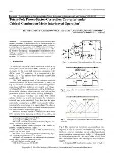
very convenient to be used as Power Factor Preregulator (PFP). Due to this fact ... Distributed power supply system used in Telecomunications. However, there ...
IMPROVING POWER FACTOR CORRECTION IN DISTRIBUTED POWER SUPPLY SYSTEMS USING PWM AND ZCS-OR SEPIC TOPOLOGIES J. Sebastian * , J. Uceda
*
, J.A. Cobos
Universidad Politecnica de Madrid. E.T.S.I. Industriales, Divisidn de Ingenieria Electr6nica. cl Jose Gutierrez Abascal.2 , 28006 Madrid, SPAIN.
*
, J. Arau *
+
*'
and F. Aldana
lnstituto de lnvestigaciones Electricas. Departamento de Elecrr6nica. Apdo. 475, 62000 Cuernavaca, MEXICO.
ABSTRACT
The Single Ended Primary Inductance Converter (SEPIC)presents several advantages over boost andjlybacktoplogies which make this converter very convenient to be used as Power Factor Preregulator (PFP). Due to this fact, both the PWM and the Zero-Current Switched Quasi Resonant gCS-QR) SEPIC used as PFP are studied in this paper. Stress in components and operm.on in conrinuos and discontinuous condum.on mode are considered in the PWM case, while the use offill-wave and half wave resonant switch is considered in the ZCS-QR case. Ihe study of the PWM SEPIC used as PFP reveals that both types of PFP control (multiplier approach and voltage-follower approach) can be used in P W SEPIC, t h e mone when it oprares in conrinuous condudon mode and the second one when it operares in discontinuous condum'on mode. Regarding the ZCS-QR SEPIC used as PFP. both types of resonant switch (halfwave andfull-wave)can be used: thefirst one presents better behaviour in losses, stresses in power transistor and diode, and switching frequency variationrange than the second one when the outputload is almost constant, but it has a high switchingfrequency variation range when it operates with very variable loads. In this case the fill-wave switch is more useful ifthe range of switching frequency variation is the primary concern. Finally the theoretical analysis is validated in two prototypes (PWM and ZCS-QR).
220 volts
AC/DC
48 volts bus
DC/DC
DC/DC
Fig. 1. Distributed power supply system used in Telecomunications. However, there are two topologies which overcomeboost and flyback converter disadvantages: SEPIC and the Cuk topologies. In this paper, we are going to analyze the behaviour presented by SEPIC topology in order to be used as Power Factor Preregulator (PFP). This analysis will include the study of SEPIC topology with PWM (no resonant) switch, and with Zero-Current-Switched (ZCS) switch working with frequency modulation. 2. DC STUDY OF THE PWM SEPIC
1. INTRODUCTION Conventional off-line switching power supply designs usually include at their input stage a full-bridge rectifier and large input filter capacitors. The problem with this input circuit is that it produces excessive peak input currents and high level of harmonic distorsionon the line. The power factor with this topology is about 0.5 - 0.7. By improving this factor, line noise and peak current levels can be dramatically reduced and the amount of power avaible to the user can be increased.
Figure 2.a shows the basic structure of a Single Ended Primary Inductance Converter (SEPIC) [ 11. The same circuit is represented in figure 2.b, but in this figure the transformer magnetizing inductance is explicitly represented by the inductance L2. Lf
Ci
The use of a Power Factor Preregulator (PFP) is the best way to get a high power factor on the line. The most popular PFP topology is the boost converter. However, the boost converter has several disadvantages: -
The output voltage is always higher than the peak input voltage. Input-output isolation cannot be easily implemented. Overload and start-up overcurrent cannot be controlled because there is no series switch between input and output.
When converteroutput is connectedto a 48 volts battery, this topology becomes useless due to these disadvantages. This fact is very common in distributed power supply systems (see figure 1). Flyback topology overcomes the above mentioned disadvantages, but also loses the location of the inductor. This location is very useful in the boost converter because the inductor current is the line current and actually provides line filtering, minimizes line noise and EM1 and allows an easy implementation of current mode control to program the input current. This work was sponsored by ALCATEL StandardElectricaS.A., Industrial Electronics and Power Electronics Research Departments.
i:n
b) Fig. 2 PWM SEPIC (a) and this same converter with the transformer magnetizing inductance @). First of all, let us calculate the average value of the current iz, i, as a function of the average output current i, i, ( ia= i because it is constant). Thus, we can write:
O-7803-OO90491/07OO-O780$01.OO 0 1991IEEE -~
7-
i,
+
4
= i, n
i, = i + i,
and, therefore: i , + i2 = n i + n i,
L~
a)
(3)
i,
Cf
Taking average values, we obtain: 1
T
i, dt
+
.
i,
= n I, +
v*
-+I 1
i,
dt (4)
0
0
L2
T
during dT
But i, and i, are flowing in two capacitors working in steady-state, and, therefore: 1
T
J i,
dt
0
i,
T
1
i, dt =
= -
o
TO
= n i, =
(5) during d'T
ni
(6)
On the other hand, we can calculate similarly the average value of the voltage vcl , vcIaas a function of the input voltage vg : v = v1 + vcl + vz
(7) during fi-d-d'lT
and taking average values, we obtain: T
I v1 dt
yI = -
T o
+
-I
vcla + I T vz dt TO
Fig. 3 EquivalentcircuitsinaPWMSEPIC.aandbinoontinrxlsoo~ mode. a, b and c in discontinuous conduction mode.
(8)
But v1 and vz are voltages in two inductors, and therefore: 1
T
f
& =
-JV1 0
1/ v 2 &= 0
(9)
TO
Assuming very low ripple in Q , equation [lo] becomes:
Equations (6) and (11) are also valid in ZCS and ZVS QRC's because no considerationshave been made about the type of switch used. The dc voltage-conversion ratio in continuous conductionmode, ,can be easily obtained from figure 3. Volts-second balance applied to the inductor can be expressed by: v (1-4 T v8dT=(12) n and, therefore:
Fig.4 Current i, waveforms. And the output voltage can be calculated by multiplyingthe average value of i, by the output load r :
where d is the duty cycle.
From equations [14], 1151 y [16], we obtain:
v
In discontinuousconductionmode, the dc voltage-conversionratio
m d z - = VI
md can be obtained averaging the current i, injected into the output cell r-cz (see reference [5]). This current can be seen in figure 4.
d
@
where K is a dimensionless parameter defined by: Volts-second balance appliedto Lz yields to the followingequation:
v d = -v d'
K =
2 Ll
rT(L,
(14)
4 +4)
(18)
n
The boundary value of K between continuous and discontinuous conduction modes, K c ,, can be easily calculated (mr = m ) :
The maximun value of i, is (from Faraday's law):
781
I I I
I
I
.
( l-d)2 -
K,
n2
(note that the values of m , md and K c , are the same in SEPIC, Cuk and flyback converters)
As usual, a SEPIC is operating in continuous conduction mode when:
K
'KaiI.
(20)
and in discontinuous conduction mode when:
K
.e
Kc*.
(21)
The waveforms in the circuit shown in figure 2.b, when it is operating in continuous conduction mode, can be seen in figure 5, in which i, and ih represent the average value of the currents i, and 4 , i, and io, the peak value of is and iD (neglecting ripple), and vsn and vh the peak value of the voltages vs and v,, . The values of these magnitudes and of the dc voltageconversion ratio m are summarized in Table 1, in which these values have been expressed as functions of the input magnitudes v, , i,, and the output magnitudes V , i . All this values canbe easily obtained from figure 3 and from equation [13]. For example, current i , flowing in the capacitor C,is i2 duringdr (fig. 3.a) and i, during d'T = (1-4 T (fig. 3.b) This current can be seen in figure5 Likewise, thepeak current value (neglecting ripple) inthe power transistor Si is the addition of i, and iz. : i,,,, = i,, + iz, = i, + i n
(22)
being i, and i related by i, = m i (power input-output balance):
From equations [13], [22] and [23] we obtain: I , = - -
n i (1-d)
- -4, d
this value can be seen in Table 1.
F i g 3 Main waveforms in the circuits shown in figure 2.b. 3. SOME CONSIDERATIONS ABOUT PFP's Figure 6 shows the general scheme of a PFP. The "resistoremulator" is a dc-todc converter working in special conditions. So, the input voltage v, is changing constantly following a line half-sine:
vs where
GI
=
v, I sinor I
(25)
is 2x times line frequency.
On the other hand, the output voltage v is approximately constant in each line half-cycle
v - v
and, therefore, the dc voltageanversion ratio is:
Table 1. Values of the magnitudes shown in figure 5. 782
--
n
(26)
V = m (or) = -
=-
V,IsinotI
v8
M IsinorI
(27)
Equation (27) showsthatthedc voltageconversionratio m is changing constantly in each line half-cycle, having a minimum value M at ot = x / 2 (peak of the half-sinusoidal input voltage) and reaching infinite a t o t = 0 and at = x (start and end of the half-sinusoidal input voltage). This is the first important consideration about the converter used as resistor emulaor: i$has a very variabk dc wltage-comrswn ratio which is constantly changing from a finite value to i@nite.
Z
Input power
p = y 1 8 2
Output power
P -
(34)
R
and from equations (32), (33) and (34) we can get the following expression for the load "seen" by the dc-todc converter in each switching frequency period:
n
r (or)
DC to DC CONVERTER
(33)
=
R -
(35)
2 sin%
The values of r (or) ace changing in each line half-cycle, having a minimum value of R / 2 ( at o t = n/2 ) and a maximum value of i n m t e ( a t or = 0 and or = z ). Figure 7 shows currents i and Z waveforms in a line half-cycle.
I
Fig. 6. Basic structure of a PFP The second important consideration is about the load "seen" by the dc-to-dc converter in each switching frequency period. The dc-todc converter shown in figure 6 has its output capacitor divided in two capacitors. Capacitor C2' has been calculated to keep the output voltage V constant during one switching frequency period, even if CZ'were the only capacitor in the dc output. Capacitor Cz", on the other hand, has been calculated to keep the output voltage V constant during each half-cycle of the input line voltage v,. In other words, C2' stores energy at the switching frequency (hundreds of kilohems) and CZ" stores energy at two times line frequency (100-120 hems); Cz' is the converter output filter capacitor and 0" is the "bulk" capacitor.
c
t
Fig.7 Current i and I waveforms in the circuit shown in figure 6.
Therefore,the dc-todc converteris working in very special conditions bemme both its ak vdtage-"ion ratio a d its I d are changing CoVLFtantfy in each line halfcycle, following the evolutions shown by equations (27) and (35) respectively.
Assuming high power factor, the line voltage and current waveforms ace in-phase sine waves, by definition. Thus, during each line half-cycle, the input current will be: ig =
zg I sin or I
This consideration is applicable to any type of dc-todc converter (PWM and resonant) working as PFP and it is very useful for determining the continuous and discontinuous conduction modes in PWM-PFP and the optimum switching frequency variation range in resonant-PFP, as we will see in the following sections.
(28)
and the input power averaged in each switching period is :
P,
= v8 i, =
vgZ,
sin20t
The output power averaged in a switching frequency period, pa is the power flowing from capacitor C2'. Its value is: 4. USING A PWM SEPIC
(30)
pa=iV
Figure 8 shows a PWM SEPIC used as PFP. In this figure, capacitor CIhas been calculated to change its voltage ( vc, ) following the variation in the input voltage vg,while capacitor Cz has been calculated to keep the
Assuming efficiency one, we obtain from equations (29) and (30): i (at) =
V
sinzor
(31)
output voltage V constant, and, therefore, includes capacitors CZ'and C2' represented in figure 6.
and, therefore, the load "seen" by the converter is: r (or) =
V = J
(or)
V,
As PFP
First of all, we are going to determine the boundaries of continuous
P z8 sin20r
and discontinuous conduction mode of operation. From equations (18) and ( 3 9 , we can obtain:
Averaging input and output power during one line half-cycle, we can obtain:
783
I
T
Equation (43) can be written as: d = @ M &
where KO = 2 L 1 4 / R T (L1+LJ is the apparent dimensionless parameter K. An important conclusionis obtained from equation (44):when a PWM SEPIC is working as PFP in discontinuousconductionmode, then the duty cycle must remain constantwhile the actual load resistanceis constant. This conclusion pushes the PWM SEPIC to " voltage follower control " when it has been designed for operating in discontinuousconduction mode. This will be analyzed in the next section.
+
, I: n
Fig. 8. PWM SEPIC used as PFP
Assuming continuous conduction mode between ot=O and ot=31/2, the values of the main magnitudes shown in Figure 5 and in Table 1 can be re-written as a function of the angle or, as we can see in Table 2. All these values have been written as functions of the constant values V,I and M.Magnitudes i, and i, represent the averagevalueofthe currentsi, and i, in a switchingfrequency period. The averagevalue of these magnitudes in a line half-cycle can be obtained by multiplying their maximum value (at or = x/2) by 2/31.
The value Of the duty cyc1e be expressed as a function of the dc voltage-conversionratio in continuous conduction mode, m ,and the line frequency, o/231, using equations (13) and (27):
d(or) =
M M+n I sin or I
(37)
And substituting equation (37) in equation (19), we obtain:
K,(or)
=
sin'or ( M + n I sin or I )'
(44)
(38)
The rms value of the current is can be calculated as follows. Approximating the waveform of i,q __ - by - a square wave-form (see figure 9), the rms value in a switching frequency period can be easily obtained from Table 2: ~
continuous conduction mode condition will then be (from expression (20)):
4 4 4
and calling KO
is,
1
>
R T( L I + ~
( M+n I sin
o r I )'
= ,i
$d = 21 @ I sinor I 4 M + n I sin or I
(39)
(45)
and de rms value in a line half-cycle from is: ,
2 L 1 4 / R T (Ll+LJ, expression (39) can be written
as: 1
2 KO >
( M+n I sin at I )'
(40) decreases when n decreases; however, Equation (46) shows that I, this fact increases io, (see Table 2) and, therefore, a compromise must be reached. On the other hand, from equation (40)we can easily obtain the condition for discontinuous conduction mode:
From expression (40) we can determine the interval of or values which the converter k Working in continuous conduction mode. Continuous conduction mode can be guaranteed for all o r values if KO verifies:
2
K a.-!-
'
2M'
KO
1
Fig. 12 ZCS-QRC switch configurations, a) half-wave and b) full-wave. 6.1
Full-wave switch ZCS-QRC SEPIC used as PFP.
The use of a full-wave switch in a ZCS-QR SEPIC used as PFP has two principal drawbacks:
Fig. 11 Input current waveforms in the boost (a), flyback (b), and SEPIC (c) topologies in discontinuous conduction mode.
6.
Referred to the first one, the energy handled by the resonant switch must be enough to provide zero-current-switching at the peak of the input current ( 0 i or i x/2 and n/2 i o f i x ). Due to the fact that the current can flow biduectionally in the full-wave switch, remaining energy is returned to the input. Both the forward excessive energy circulating from the input to the output and the reverse remaining energy circulating from the output to the input, cause high conduction losses in the resonant switch ( switch and resonant capacitor and inductor ). This problem is overcome by using a half-wave switch, because current can only flow unidirectionally and, therefore, reactive energy can not be handled.
USING ZERO CURRENT SWITCHED QUASI-RESONANT SEPIC AS POWER FACTOR PREREGmATOR.
The demand for smaller and ligther power converters in pushing switching frecuencies higher and higher. Such high switching frequencies are made possible using resonant topologies. In particular, Zero Current SwitchedQuasi-resonant converters(ZCS-QRC's), [2], [3], areveryuseful in the range of 50-200 watts and 0.5-1.5 MHz. There are two typesof ZCS-QRC's, depending on the implementation of the resonant switch (see Figure 12):
-
A lot of reactive energy is handled by the resonant circuit. A high switching frequency variation range is required to obtain a high power factor in the input line, with low stress level in the switch and in the diode.
ZCS-QRC with "half-wave"switch configuration, in whichthe current can only flow in the forward direction. ZCSQRC with "Full-wave" switch configuration, in which the current can flow bidirectionally.
W h reference to the second one, let us analyze the switchingfrequency variationrangeusingafull-wave resonant switch. If weassumepower factor "l",the value of n(ot) must reach infinite. However, maximum values of about 6M allow high power factor (0.9988) and 5% of total harmonic distorsiOn(see~[4]).Ifthemaximumvalueofm ( o f ) is pM(l