Kuon, R. Tessier, and J. Rose"FPGA Architecture: Survey and Challenges", now Publishers Inc., 2008. [2] National Instruments Co, "Cycle-Accurate Co-.
International Journal of Computer Applications (0975 – 8887) Volume 91 – No.12, April 2014
Interfacing Force Sensor to on Board ADC of Spartan3E Mustafa Salim
Rafid Ahmed
University of Mosul Iraq
University of Mosul Iraq
Force sensor from interlink that use square pad forforce sensing is useful for many applications, as the resolution of this sensor continues and FPGA is digital, an ADC is required to deal with such sensor and as the embedded ADC of Spartan 3E kit need complex signals synchronization to work.This paper present a hardware design and optimized implementation based VHDL coding of control unit that make the ADC of Spartan 3E kit operate in real time. The system use Moore states machine style for generating ADC synchronization signals. Also, the result observed via new approach, which is instead of using chip scope for displaying values of ADC, LabVIEW FPGA environment is used so it‟s possible to display result on PC via USB. The control is optimizedand efficient due to using only 1% of FPGA chip and the measured force can be displayed in real time and the proposed control unit can be work as standalone or coprocessor architecture.
The disadvantage of approach is that the chip utilization report based on our LabVIEW FPGA in the lab for (ADC unit only) consumed about 25%. In [7] S.Chaurasiaprsesnt an interface unit of the embedded ADC and the results were observed via ChipScope-Pro and LEDs also they provide VHDL code base on states machine for such unit and our FPGA synthesis report of code indicate that the chip utilization about 4%. in this paper, a hardware design and implementation based VHDL coding of control unit is presented that able to synchronize signals of embedded ADC of Spartan 3E with displaying the result on PC via LabVIEW FPGA environment that provide direct method for connecting between chip and PC via USB.2 with only 1% FPGA chip utilization. This paper is divided into three sections: section two describes the force sensor operation, section three shows the hardware implementation and how each ADC signals synchronized with result, section four presents the conclusion, five and six give reference and VHDL code of the control unit respectively.
ABSTRACT
General Terms FPGA, VHDL, LabVIEW FPGA, Force, Sensor.
Keywords FPGA, Analog to Digital Convertor, Spartan 3E FPGA, Force Sensor, FSR, Programmable Pre-Amplifier, LTC 1407A, ADC, Labview FPGA.
1. INTRODUCTION Force sensing resistor from Interlink is the most versatile force sensing technology on the market today. These innovative sensors provide a response in resistance with an increase in applied force. These sensors provides engineers and designers with a durable, reliable, easy to measure and low cost solution for human machine interface touch [1]. The FPGA [2] with reconfigurable logic feature, portability, low consumption of energy, high speed and large memory for data storage are great for use for development of complex applications. FPGA configuration based VHDL [3] coding allow us to develop specific hardware architectures with maximum flexibility. This specific feature of the VHDL that give high degree of design anatomy comparing to others implementation methods.LabVIEW FPGA [4] isnew hardware design tool that can be used to design different systems, LabVIEW FPGA provide different features such easy hardware component synchronization and interfacing between PC and Spartan 3E FPGA chip.In the literature several control units of embedded ADC proposed. In [5]IstiyantoJ.Epresent a design of a controller based states machine using VHDL for the amplifier and the embedded ADC and tested it using a function generator and an oscilloscope and the chip utilization was3%. Also in [6] G. Crouch from National Instruments provide a control unit of ADC with signal filtering based on pure LabVIEW FPGA environment and display the filtered result on PC using USB.
2. FORCE SENSOR OPERATION The basic force sensing resistors consists of two membranes separated by a thin air. The air gap is maintained by a spacer around the edges and by the rigidity of the two membranes. One of the membranes has two sets of interdigitated fingers that are electrically distinct, with each set connecting to one trace on a tail. The other membrane is coated with FSR ink. Around the perimeter of the sensor is a spacer adhesive that serves both to separate the two substrates and hold the sensor together. The inside surface of one substrate is coated with FSR carbon-based ink. When the two substrates are pressed together, the microscopic protrusions on the FSR ink surface short across the interdigitatedfingers of the facing surface [8].
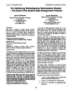
3. H/W IMPLEMENTATION The block diagram of entire implemented system shown in Figure (1).It consists of force-to-voltage conversion, embedded amplifier,ADC and signals controller base on states machine that consist of two main states and several sub states that are synchronized together to generate specific time signals transaction.The Spartan 3E FPGA includes a two channel analog capture that is consisting of a programmable amplifier and ADC. The analog circuit captureand convertthe voltage on VINA or VINB on board to a 14-bit digital at the same timeunder the following [9]: ADC [13:0]=8192*GIAN*(Vin-1.65 v)/(1.25 v) …… (1) The gain is the current setting that is loaded into the amplifier. The allowable setting for gain and allowable voltages applied to VINA and VINB inputs appear in table (1)[9]. For example if gain set to -1 then the input voltage range will be with 0.4v as minimum and 2.9 v with maximum. Figure (2) show two examples that both represent the ideal responseof the analogue inputs.In order to program the amplifierby using
6
International Journal of Computer Applications (0975 – 8887) Volume 91 – No.12, April 2014
Inside Spartan 3E kit PC
USB
USB-JTAG
Display the measured force
FPGA Control Unit SPI master
SPI based ADC slave
SPI based amplifier slave
Force sensor Fig.1: Complete system [initial graph was taken from [9]] Table 1. Range selecting Gain
A3A2A1A0
value
B3B2B1B0
-1
0
0
0
1
-2
0
0
1
0
-5
0
0
1
1
Fig 2: Ideal response of the ADC.
SPI signalsthat must be carefully controlled and generated in specific time. These signals include: SPI_MISO, SPI_SCK and AD_CONV [9].Figure (4) showthe simulation timing diagram of the communication process of the implement control unit with ADC where the signal SPI_MISO (SPIMaster Input Slave Output) set as „1‟. The system only read the VINA channel most significant bit first during first 16 SPI_SCK cycle and ignore VINB.As shown in figure (4) when the AD_CONV signal goes high for limited time then goes low the ADC simultaneously capture (VINA and VINB) at the same time. The next captureand conversion are not presented until the next AD_CONV is goes and low again so the frequency of this signal control the sampling frequency of the embedded ADC. The signal frequency can be controlled through using single NOT gate, comparator and counter that all already available in the proposed control unitand the value that will compared with the counter output value can be changed [refer to VHDL code sampling frequency].The ADC presents the value of the samples as 14 bits two‟s complement [9]. The embedded ADC requires at least 34 cycles of SPI_SCK [9]that must be distributed as two 14 bits (significant bit first) for channel VINA and VINB and the remaining 6 cycles are not used. The SPI bus signals are shared by other devices on the same board. The other devices must be disabled [9] and it were disabled as shown in figure (5).
FPGA withselected gainvalue from table (1(; three SPI signals (AMP_CS. SPI_MOSI and SPI_SCK) must be generated under specifictiming.The amplifier programing starts when the FPGA asserts AMP_CS signal to Low; the amplifier captures serial data on SPI_MOSI (Master Output Slave Input) on the rising edge of the SPI_SCK clock signal [9]. Figure (3) shows timing diagram of the communication process of the implement control unit with amplifier with sending specific gain [00010001](send bit by bit) that give maximum input voltage range.For any bit transmission and reception in SPI protocol it relative all to SPI_SCK also, as the control unit based on states machine with two main states and several sub states; it can beseenfrom figure (3) that thestarting main state of the unitis amp_states. The gain of amplifier must be sentas an 8-bits consisting of two 4-bits. The most-significant bit B3 is sends first. After amplifier gain programing, the next step is to read from ADC and in order to read by usingFPGA; there are three basic
Fig 3: Control unit communication with amplifier
7
International Journal of Computer Applications (0975 – 8887) Volume 91 – No.12, April 2014
Fig4: Control unit communication with ADC. Table 2: FPGA utilization report.
Fig5: Disabling the other devices through setting on or off value to specific signals. After successful control unitdesign and implementation developing using ISE environment [10], The VHDL code was merging in LabVIEW FPGA environment so the real time ADC acquisition of force sensor can displayed on PC with coprocessor architecture as shown in figure (6). Several different force (voltages) changes over time at sensor pad are captured displayed in real time at chart indictor of LabVIEW software as shown in Figure (7). Only the most 8 significant bits was taken from VINA channel. The chip utilization report shown in table (2).
Logic Utilization
Utilization
Number of Slice Flip Flops
1%
Number of 4 input LUTs
1%
Number of occupied Slices
1%
4. CONCLUSION This paper present a hardware implementation based VHDL of controller unit that make the embedded ADC of Spartan 3E kit operate, The design of amplifier and controller based on Moore states machine and due to that the unit is optimized as it using only 1% from silicon area of the chip. The adopted on chip verification with coprocessor architecture that required merging of VHDL with LabVIEW FPGA contribute in reducing the complexity associated with traditional on chip verification like the chip scope also, as have been noted that the on bored ADC of Spartan 3E kit very affected by the noise and only the most significant bits can be used.Our future works are to connect force sensor to robot arm end effector and developing a control unit for embedded Spartan 3E digital analog converter with proposing embedded real time digital signal processing algorithms such adaptive filter in FPGA.
5. REFERENCES Fig 6: The adopted hardware test approach
[1] Online article at http://www.interlinkelectronics.com/products.php. I. Kuon, R. Tessier, and J. Rose"FPGA Architecture: Survey and Challenges", now Publishers Inc., 2008. [2] National Instruments Co, "Cycle-Accurate CoSimulation with Mentor Graphics ModelSim", white papers, Nov 09, 2012. [3] V. A. Pedroni"Circuit Design with VHDL ", MIT Press, 2004. [4] Online article at https://www.ni.com/fpga.
Fig7: Different force pressure at sensor
[5] IstiyantoJ.E,"A VHDL-based ADC on FPGA", IEEE International Conference on Instrumentation, Communications, Information Technology, and Biomedical Engineering, Bandung, 23-25 Nov. 2009, pp. 1 -3.
8
International Journal of Computer Applications (0975 – 8887) Volume 91 – No.12, April 2014 [6] G. Crouch "National Instruments LabVIEW FPGA Training for the Spartan-3E XUP or NI R-Series Hardware",May 08, 2013. [7] ShobhitChaurasia"IMPLEMENTATION OF THE ONBOARD ADC ON SPARTAN 3E FPGA PLATFORM "Department of Computer Science and Engineering,IIT ,Guwahati, Jun 2012. [8] Interlink Electronics, integration guide.
"Force
Sensing
Resistors",
[9] Xilinx Co. "Spartan-3E FPGAStarter Kit BoardUser Guide", UG230 (v1.2) January 20, 2011. [10] Xilinx Co."ISE Synthesis and Simulation Design Guide", UG626 (v 14.1) May 8, 2012. [11] K. Chapman, “Picoblaze: amplifier and A/D Converter Control forSpartan-3E Starter Kit”, 2006.
6. APPENDIX VHDL code Here is our VHDL code that can display the captured voltage at 8 bits LEDs of onBoard Spartan 3E. --- 30/6/2013 library IEEE; use IEEE.STD_LOGIC_1164.ALL; use IEEE.NUMERIC_STD.ALL; useIEEE.std_logic_arith.all; entity spartan3e_adc is port ( clk : in std_logic; --- 50MHZ defultspartan 3e clock SPI_MISO : in std_logic; --- read from ADC enable : in std_logic; --SPI_MOSI : out std_logic; --- for gain value SPI_SCK : out std_logic; --- write/read values during edges of this signal AD_CONV : out std_logic; --- control the sampling rate of ADC AMP_CS : out std_logic; --- must be zero during gain set only leds : out std_logic_vector(7 downto0); SPI_SS_B : out std_logic; SF_CE0 : out std_logic; FPGA_INIT_B : out std_logic; DAC_CS : out std_logic; SF_OE : out std_logic; SF_WE : out std_logic) ; end spartan3e_adc; architecture Behavioral of spartan3e_adc is signalen,x : std_logic := '0'; ------------states machine decleration----------------type state_type is (amp_states, adc_states); type amp_state_type is (amp_s1, amp_s2, amp_s3,amp_s4);-amplifier sub states type adc_state_type is (adc_s1, adc_s2,adc_s3,adc_s4); -ADC sub states signal state : state_type := amp_states; signalamp_state : amp_state_type := amp_s1; signaladc_state : adc_state_type := adc_s1; -----------------------------------------------------------signalvina_inedx : integer range 0 to 16; --- index for incomming ADC serial data. begin SPI_SS_B