SPECIAL SECTION ON SECURITY AND RELIABILITY AWARE SYSTEM DESIGN FOR MOBILE COMPUTING DEVICES
Received December 9, 2015, accepted January 27, 2016, date of publication February 3, 2016, date of current version March 30, 2016. Digital Object Identifier 10.1109/ACCESS.2016.2524447
Introducing TAM: Time-Based Access Memory NAGI N. MEKHIEL, (Senior Member, IEEE) Department of Electrical and Computer Engineering, Ryerson University, Toronto, ON M5B 2K3, Canada (
[email protected])
ABSTRACT The increase in processor speed achieved by continuous improvements in technology is causing major obstacles to the parallel processors implemented inside the chip. The time spent in servicing all the cache misses from all processors from a slow shared memory limits the performance gain of parallel processors. We propose a new memory system that makes all of its content available to processors, so that processors need not to access the shared memory in a serial fashion. Rather than having one processor access a single location in the shared memory at a time, we force each location to be available to all processors at a specific time. This new memory system is fast and simple, because it does not need decoders and can use the DRAM or SRAM technology efficiently as the access of each location is known ahead of time. Results show that this new memory improves a single processor performance by 350% and the performance of eight parallel processors by 2400%. The new memory decouples the slow memory from the fast processor and makes the parallel processors scalable to an infinite number of processors. INDEX TERMS Memory organization, DRAM, scalability of multiprocessor, synchronization, data access modes.
I. INTRODUCTION
Conventional memory uses an array of cells and could be accessed by only applying one address through a decoder. Only one memory location is selected through the decoder. The performance of a processor depends on its memory system [1], [2], [3]. New processors use a large multi-level cache system to close the huge speed gap between processor and main memory DRAM [17]. According to Amdahl’s law the performance improvements of an advanced processor is limited by the slow portion that cannot be improved which is cache misses to DRAM. There have been efforts to improve the performance of the DRAM memory system. One of these efforts yielded the Synchronous DRAM (SDRAM). SDRAM uses multiple banks and a synchronous bus to provide a high bandwidth for accesses which use the fast page mode. With multiple SDRAM banks, more than one active row can supply the processor with fast accesses from different parts of memory [5]. The performance of SDRAM still cannot satisfy the requirements of new processors because it has long latency for the first access and its data transfer rate is limited by the bus speed. Direct Rambus DRAMs (DRDRAM) uses a fast bus that transfers on both edges to achieve maximum bandwidth [6]. DRDRAM uses many banks as in relation to SDRAM of the same size. In DRDRAM each sense-amp is shared between
VOLUME 4, 2016
adjacent banks that cannot simultaneously be in different open pages thus increasing fast page miss rate compared to one open row per bank in SDRAM. The timing of DRDRAM is similar to the other DRAM organizations and suffers from the long latency of first access. Another effort yielded the Cached DRAM (CDRAM) [7], [8]. This design incorporates an SRAM-based cache inside the DRAM. Large blocks of data can thus be transferred from the cache to DRAM array or from the DRAM to cache in a single clock cycle. However, this design suffers from problems of low cache hit rate inside the DRAM caused by the external intercepting caches. It also adds complexity to the external system for controlling and operating the internal cache requiring a cache tag, a comparator and a controller. In addition, there is a significant cost in terms of die area penalty for integrating SRAM cache with a DRAM in a semiconductor manufacturing process. A much faster and efficient memory would have its contents available outside so that each cell could be accessed at a specific time. This new memory is simpler because it does not need any addresses or decoders and is fast because each access is known ahead of time and can hide the access time overhead. We call this new memory Time Based Access Memory ‘‘TAM’’ because all memory locations are mapped in time and not in space.
2169-3536 2016 IEEE. Translations and content mining are permitted for academic research only. Personal use is also permitted, but republication/redistribution requires IEEE permission. See http://www.ieee.org/publications_standards/publications/rights/index.html for more information.
1061
N. N. Mekhiel: Introducing TAM
II. BACKGROUND
Although the memory speed gap has not been solved, processor designers are continuously improving the speed of processors using fast technology and implementing advanced architectures like simultaneous multithreading and multiprocessor on a single chip [12]. To improve the performance of applications by executing multiple instructions in parallel, multiprocessor systems have been used for many years when the memory speed gap was not as critical [4], [13]. One popular architecture is the multiprocessor with shared memory. The sharing of one memory and the synchronization overhead for managing the shared data limits the performance gain and scalability of the system [1]. A single processor was developed to execute parallel threads to make full use of the single processor resources [12], [15], [16]. Intel Hyper-Threading makes a single physical processor appears as two logical processors [12]. Threads could be scheduled to the logical processors and run in parallel as in multiprocessor system to improve system performance. The Intel Xeon with hyperthreading running online transactions [12] shows that for two parallel threads, the system gives performance improvements of only about 24% compared to the performance of running the two threads in a single processor. Processor designers are now using multiprocessors in a single chip [14], [19], [20]. The Intel multiprocessor with two parallel processors has performance gain of only 55% compared to a single processor. For four parallel processors, Intel system improves performance by only 160% [12]. Conventional multiprocessor systems cannot be made scalable to a large number of processors although future applications demand the computing power of thousands of processors [18]. Hence, we must focus in solving the root cause of this problem which is the sharing of memory. From the above, we find that neither multithreading nor multiprocessor architectures are utilized to their full potential. The slow shared memory and the synchronization overhead limits the performance gain and scalability of these systems. In multithreading and multiprocessor systems, the performance gain is achieved by overlapping the execution time of one processor with the execution time of another processor. Decreasing the execution time alone is not effective if the processor has to wait longer for accessing the slow shared memory. For example, if the processor execution time is 1 unit, and the waiting time is 2 units, then the two parallel processors can only reduce time by 1/2 of the execution time. This gives a gain of only 3/2.5 or 20%, although the execution time improves by 100% (Amdahl’s law). The performance of multiprocessor systems is limited not only by the slow shared memory but also by the synchronization overhead. To reduce the synchronization overhead, Transactional memory has been proposed to reduce the overhead of synchronization as it uses large sequential code to run as one serial atomic transaction [10], [11]. Lock based critical sections used for synchronization in conventional 1062
multiprocessors have significant performance overhead and Transactional Memory lock removal can eliminate the overhead by using lock-free sections [10], [11]. The cost of overhead from supporting Transactional memory is only about 10%, compared to about 40% for locks. The reduction in overhead for eliminating locks suggests that supporting parallel code has a cost that could limit performance gain of parallel processing. The improvement from using transactional memory is also limited and cannot make multiprocessor systems scalable to a larger number of processors because it does not completely eliminate synchronization and still suffers from the sharing of slow memory. From all of the above discussion, it is very clear that neither the industrys new products using chip multiprocessor (CMP) and simultaneous multithreading (SMT) nor the academic research can offer the computing power needed for future applications. Therefore, we need a non-evolutionary solution to deal with the fundamental problems of memory and synchronization. The best solution will be a single solution for both problems. We have invented a TIME BASED ACCESS MEMORY that maps its content to time for a scalable parallel system [9]. III. MOTIVATIONS
We propose a new memory system that can satisfy an infinite number of parallel processors. This new memory eliminates the problems of sharing a slow memory and the overhead of synchronization. The motivations for the new memory include the following:• The time spent to access the main memory limits the performance of processors according to Amdahls law. Typically 80% of the processor time is spent waiting for the slow memory. Faster memory is essential to processor performance. • Conventional memory maps each data element to one specific location in the memory array and can only be accessed by applying a single address through its decoder. This memory is slow because it cannot be accessed for more than one location through the single decoder that has a decoder delay. • The performance of a multiprocessor ‘‘multi-core’’ system, is limited and cannot be made scalable for a large number of processors because of sharing a slow memory as well as the synchronization overhead. • The increase in processor speed achieved by the continuous improvements in technology causes major obstacles to the parallel processors implemented inside the chip. The overhead (using locks) for running multiple threads on a shared external memory might far exceeds the time saved by overlapping the execution time among parallel processors. Current architectures cannot make a parallel processor scalable. • Conventional multiprocessor systems have multiple cache misses to one memory location. This further increases the demands for accessing the slow memory. VOLUME 4, 2016
N. N. Mekhiel: Introducing TAM
•
•
•
•
Conventional cache transfers multiple words on a block for each miss. This increases the transfer time to access memory. Number of cache misses increases linearly with number of processors. This limits the scalability of the parallel processor because it increases memory waiting time. Number of cache misses increases with the size of an application, causing proportional increase to time spent in memory. Time spent to service all the cache misses in the life of an application could exceed the time spent to deliver the contents of the whole memory to the processor.
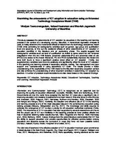
FIGURE 1. TAM concept.
IV. TAM CONCEPT
A shared resource will become available if it is offered to all processors. Processors then need not to arbitrate and wait to get the data from the shared resource. Rather than having one processor to access one location in memory at a time, we allow all locations to be available to all processors all the time. The processor waits for the memory to provide its data or instructions at a specific time. If we make each processor accesses the data at a specific and known time, then there is no need for synchronization among multiple processors because the access to a specific location is known for all processors. We propose making the contents of memory available to all processors using a shared bus. Every location in the memory is guaranteed to be delivered to the bus and all processors have all the requested data available after waiting for a time that does not exceed the time of transferring the whole memory out in the bus. The new memory makes its content continuously revolve around the bus, so that any processor can access the data at a specific time. TAM consists of the following features:• It supplies all contents of memory to all processors regardless if the processor needs it or not. • TAM is very fast because it is accessed sequentially in time and does not have to use a random access mode as in conventional memory. • The access of each DRAM location is known ahead of time, so there is no waiting time for precharge, or decoding, therefore access time is hidden. • TAM uses DRAM or SRAM technology with a very simple organization. Figure 1 shows a block diagram for the TAM concept. The contents of memory continuously revolve in a fast speed and can be accessed by any processor. The memory address is time and it becomes TIME ADDRESSABLE Memory. Figure 2 shows the access time of TAM. The first access to location 0 waits for row activation by a Start signal, then in each cycle the content of one location is accessed and data is read or written to this location. In a serial fashion, the next location becomes available and is accessed in the next clock cycle until the last location in memory. After the last VOLUME 4, 2016
FIGURE 2. TAM access timing.
location becomes available to be accessed, the first location is accessed next and this continues in a cyclic form. V. TAM ORGANIZATION AND OPERATIONS
TAM could be implemented in DRAM technology or any other technology. It also has potential to be implemented using a different organization than the known array structure to optimize the cost of implementation. We assume using the known DRAM technology to implement TAM and the contents of DRAM is accessed sequentially in a serial fashion without the need for an address or decoders. Because the time to access each location is known ahead of time, the activation time overhead is hidden and overlapped among the different DRAM banks. The access time for each location will be only the time of accessing the sense amplifier and is limited only by the external bus speed. There is no address lines, and the TAM DRAM will use the address lines to transfer more data which will double TAM DRAM bandwidth. Figure 3, shows the organization of TAM. It consists of the following components: • DRAM Array: Organized as an array of N rows by M columns. Each cell is located at the intersection of a specific row and a specific column. The storage cell consists of one capacitor and one transistor as in any DRAM structure. 1063
N. N. Mekhiel: Introducing TAM
FIGURE 3. TAM organization.
FIGURE 4. Row shift register.
FIGURE 5. Column shift register.
•
•
•
•
1064
Row Shift Register: Has N outputs, each is responsible to activate the corresponding row similar to the row decoder outputs in DRAM. The Row shift register consists of N D-type Flip Flop and its design is given below in Figure 4. Column Shift Register: Has M outputs, each corresponds to a column selection output that allows the flow of data similar to the column decoder outputs in DRAM. It also uses a D-type Flip Flop and its design is given below in Figure 5. Sense Amplifiers: Used to access the data from the input output DO/DI signal as in DRAM. The direction of data flow is controlled by a /WE signal as in any DRAM. Time Control: Uses the state machine, given below, in Figure 6, to provide the following signals: – Start-act-ROW: This initialize first D-Flip-Flop to be active for the Row Shift Register. – Row CLK: Clock for the Row Shift Register. The period of this clock defines the time for the row to stay active. Each Row clock period, the Row Shift Register activates the next row by shifting the active output of a Flip-Flop to the next. – Start-shift-COL: This initializes the first D-Flip-Flop to be active for the Column Shift Register.
FIGURE 6. State diagram for TAM control.
– COL CLK: Clock for the Column Shift Register. The period of this clock defines the length of time for the column to stay active. Each clock period, the Column Shift Register activates the next column by shifting the active output of a Flip-Flop to the next. – /WE: Write enable signal, when it is active, the latches of sense amplifiers are updated with the value of data input in DI. On memory read, this signal becomes not active and the data from the sense amplifier are transferred to the output signal, DO. A. ROW SHIFT REGISTER
Figure 4 shows the block diagram of the Row Shift Register. This shift register shifts right and rotates the content of the register. Every clock cycle, only one Flip-Flop output becomes active that corresponds to the activation of the next row in memory. It consists of N of D Flip-Flops, all connected to one clock, ROW CLK. On start or when Power-ON is active, all Flip Flops are cleared to 0, except the first Flip Flop to the left. The first Flip-Flop is connected to the Start-act-ROW signal which becomes active on the start of the activation of the first row in memory of the memory array, and it becomes active again after the rest of the memory is accessed (cyclic operation). For memory expansion, the Start-act-ROW is connected to the LAST ROW signal generated from a previous memory chip Row Shift Register. TAM memory expansion is given below in Figure 7. B. COLUMN SHIFT REGISTER
Figure 5 shows the block diagram of the Column Shift Register. The shift register shifts right and rotates the content of the register. It consists of M D Flip-Flops for M columns DRAM, all connected to one clock, COL CLK. On start or Power ON, all Flip-Flops are cleared to 0 with the POWER ON signal VOLUME 4, 2016
N. N. Mekhiel: Introducing TAM
FIGURE 7. TAM memory expansion for basic system with fixed access patterns.
•
connected to clear each Flip-Flop. After waiting for the start activation of a row, every clock cycle, one Flip-Flop output becomes active to access the next column in the accessed row in memory. The first D Flip-Flop to the left, is connected to the Start-shift-COL signal which becomes active on the start of the activation of the first column, after waiting for the row to column time delay, and it becomes active again after the last column is accessed as it is connected to CLM signal generated from the Flip-Flop of last column. C. TAM CONTROL AND OPERATIONS
Figure 6, shows the state diagram of TAM Time Control. The state machine is responsible for the following:• Power On: On state S0, the circuit waits for the Power On signal to start from the power off condition. • Initialization: When the Power On signal becomes active, the circuit starts with the initialization process as in any DRAM, then it waits for the Start-act-ROW signal to become active on state S1. • Row Activation: When the Start-act-Row signal becomes active, the circuit makes the ROW CLK voltage level high, for one clock cycle on state SR0, then it goes to next state SR, and makes the ROW CLK level low. This generates a full ROW CLK cycle, while the input of the first Flip-Flop of Row Shift Register has its D input = 1 as it is connected to the Start-act-Row signal. At state SR0, the output Q of this Flip-Flop which is connected to Row 0, goes active and starts Row0 activation. • The state machine waits in state SR, until the end of accessing all the columns in this row. Signal CLM, becomes active from the output of the last Flip-Flop of Column Shift Register. When signal CLM becomes active, the state machine goes to state SR0 to start the next row activation. • When the CLM signal is received and the state machine goes back to SR0, it makes the ROW CLK signal high, and this causes the Row Shift Register to shift right the 1 from the current Flip-Flop to the next one, causing next row output R1 to become active. The state machine goes through the same states as above for the rest of the rows. • Generating COL CLK: The state machine is used as a frequency divider of the main clock signal to generate VOLUME 4, 2016
•
•
•
COL CLK, which its cycle time depends on the speed of DRAM. The speed is determined by the time needed to transfer data in or out of the sense amplifiers. On state SCLK0, the state machine makes COL CLK high, then it goes to a next state, in the middle of states, the state machine makes COL CLK low then it goes to the next states to complete a full cycle. At the last state, SCLKN, the state machine goes back to SCLK0 to start the next clock cycle. This is a typical frequency division method using state machine. Accessing Columns: When the Start-act-Row signal becomes active, the circuit goes to state SR0, and makes the row active and simultaneously, it goes to state SCD to start the column access. The column access process goes through the number of states to allow for TRCD before activating the first column in the active row. After waiting for TRCD, the state machine goes to state SC0 and it generates a Start-shift-COL signal that is connected to the input of the first Flip-Flop of the Column Shift Register. This is while the COL CLK is being generated, and on its rising edge, the first Flip-Flop of column shift register will have its output Q=1, which is connected to column CL0 signal to access the first column in the row. The shift register keeps shifting the 1 on each cycle of COL CLK thus activating the next column until it reaches the Flip-Flop connected to the last column. Signal CLM, becomes active from the output of the last Flip-Flop of the Column Shift Register. When signal CLM becomes active, the state machine goes to state SR0 to begin the next row activation. READ/WRITE: After activating the specific row and accessing a specific column as specified above, the /WE signal controls the direction of data flow from the sense amplifier to or from DO/DI. In a READ operation, /WE is kept ‘high’ during column access time, and the data flows from the sense amplifier to the DO. In a WRITE operation, the /WE signal is asserted ‘low’ during the column access time, and data from DI is written to the sense amplifier latch. The timing of the READ/WRITE operation depends on the DRAM speed and is similar to known DRAM read or write operations. Refresh: Refresh is easily provided by the cyclic nature of accessing all the rows in a sequence. The time control circuit monitors the rate at which all rows are activated and starts a refresh cycle if the time interval of the last row activation exceeds the maximum required refresh time. At the end of the row activation and when the LAST ROW signal becomes active, the state machine goes to state SRF0. It then increments the refresh counter and it proceeds to state SRF1. In state SRF1, the content of that counter is compared to the maximum refresh time and if the counter time is less than the refresh time, the state machine goes to state RF0 and repeats the above. 1065
N. N. Mekhiel: Introducing TAM
In state RF1, if the counter indicates that the refresh count is equal to or exceeds the maximum refresh time, the state machine goes to state SR0 and starts activating all the rows. Other conventional refresh operations could be used in TAM. VI. DESIGN OF DIFFERENT MEMORY SYSTEMS BASED ON TAM A. TAM MEMORY WITH FIXED ACCESS PATTERN
Figure 7 shows the basic memory system that uses multiple TAM chips to expand the memory. The basic system consists of multiple TAM memory chips connected in a serial fashion such that the first location starts from the first location of the first chip and the last location is from the last location of the last chip. After accessing the last location of the last chip, the access of the first location of the first chip occurs as shown in the block diagram. All memory chips are connected to the same CLOCK signal for synchronous design. All DO/DI signals are connected to the same bus signals as in any conventional memory expansion. The /WE signal is connected to /WE in all the chips. The expansion of the memory system is very simple because it needs only one signal to be connected from one TAM to the next TAM memory chip. The LAST ROW signal from one chip is connected to the Start-act-ROW input of the next chip. Conventional memory expansion needs to decode some address lines to access the extra memory. This decoder adds to the system complexity and delay. The operation of memory starts with the first chip in the system. The Start-act-ROW input of the first chip is activated either by POWER-ON or by the LAST ROW signal of the last chip as shown in figure 7. The POWER-ON signal is needed for starting memory access for the first time after Power Off. The POWER-ON signal is generated from a special circuit that gives a pulse when the supply voltage changes from 0 to 1 on POWER-ON. The LAST ROW signal of the last chip activates the first row of the first chip through the feedback signal that is connected to the OR gate. The data is read or written to each cell based on the value of the /WE signal. If the DRAM single chip is organized as N Row by M Column, and the memory system consists of K chips, then the total number of memory storage = NxMxK locations. It will take NxMxK cycles to access the full memory, and accessing the memory repeats every NxMxK cycles in a cyclic serial fashion. The cycle time for TAM is much faster than accessing conventional memory as it does not have a decoder and it hides the Row and Column activations time by overlapping it with data access time. B. TAM MEMORY WITH ADAPTABLE ACCESS PATTERNS
In the basic TAM memory system with fixed access patterns, the access of memory starts from the first location of the first chip and ends at the last location of last chip. The number of locations to access in a memory cycle is always fixed. The time to complete a memory cycle includes waiting for all 1066
memory locations to be accessed as mentioned above. The processor must wait until the location it needs to arrive. Figure 8 shows TAM memory system that is adaptable to the demands of a processor and can change its access patterns. The adaptable system uses a control circuit to determine which chips to access. The control circuit uses a start address to select the first chip and a second address to select the last chip. The address lines is log base 2 of the number of chips.
FIGURE 8. TAM memory system with adaptable access patterns.
To explain the operation, let us assume that the number of chips is 16 where each DRAM chip has 64 million locations, and the processor needs to access a memory section that starts from location 193 million to location 520 million. The starting address will be chip number 4 (193 divided by 64). The last chip address will be chip number 9 (520 divided by 64). Only chips 4, 5, 6, 7, 8 and 9 are accessed. The CONTROL circuit will make Start4 output signal active through decoding the start chip address from the processor. This is a pulse and only becomes active at the start of the memory access operation. It becomes active again when the LAST ROW signal of the last chip to be accessed (chip 9) becomes active. The following conditions make Start4 active:• The Decode of Start Address 4. This is only active for a time that is enough to start memory access similar to POWER-ON time. • The Decode of End Address 9 AND LAST-ROW-ofchip 9 becomes active to allow the cyclic action of memory access. • The CONTROL circuit decodes the END-chip address 9, and activates all the End signals of the chips from chip 4 to chip 9. Furthermore, End4, End5, End6, End7, End8 and End9 becomes active. The conditions to make any End signal active is:– The chip number is equal or greater than the Start Address 4 AND LESS THAN OR EQUAL TO the End Address 9. The design of such a circuit is simple and could use a combination of a comparator, decoder and encoder. VOLUME 4, 2016
N. N. Mekhiel: Introducing TAM
C. TAM MEMORY WITH ‘OUT-OF-ORDER’ ACCESS PATTERNS
The adaptable TAM system, explained above, has the following limitations:• Accessing of different locations must be in order, starting from first location of first accessed chip to the last location of the last accessed chip. • The first accessed chip and length of memory locations to be accessed are fixed during the memory access cycle. This means that during accessing the memory, we cannot change the order of accesses. In the above TAM system the accesses are to chip4, followed by chip5, .. the last is chip 9. We cannot have accesses to chip 4, followed by chip 7, followed by chip 5. To deal with ‘Out-of-Order’ access patterns and to solve the memory fragmentation, the following TAM memory system organization is used. Figure 9 shows a block diagram of TAM ‘Out-of-Order’ ACCESS organization. We assume that each chip consists of multiple banks, and each bank contains several memory rows. For example, a DRAM that has 1024 ROWS could be divided to 32 banks where each bank contains 32 rows. The number of locations in each bank depends on the number of columns in each row.
To support ‘In-Order’ access patterns, this unit has a counter that counts from 0 to the number of banks. The counter output is connected to the decoder. If the mode is set for IN ORDER ACCESS, then the decoder decodes the output of the counter. Memory expansion with ‘Out-of-Order’ access patterns is simple and uses a memory controller that selects the start of the next chip based on a chip select address similar to bank select address. The controller waits for the LAST ROW signal from the current accessed chip and decodes the chip select address, then it generates the start activation of the row for the selected chip. The start signals of the rest of the chips are forced to be not active and these chips cannot start any access. D. TAM MEMORY WITH MULTIPLEXER/DE-MULTIPLEXER
In the Out of Order TAM, one bank at a time is accessed while the rest of the banks are waiting. This design is simple and could save power, however it cannot support parallel accesses from memory. Another organization that uses multiplexers can allow data in each bank to spin around in cyclic form and creates a parallel data accesses between each bank (explained below). Figure 10 shows the TAM organization using a multiplexer and demultiplexer. The select bank address selects the specific bank to be accessed among the multiple banks. It allows output data DO of the specific bank to pass through the multiplexer to the memory bus. It also allows the input data, DI from the memory bus to be passed through the demultiplexer to be written to the selected bank.
FIGURE 9. TAM memory system with ‘out-of-order’ access patterns.
Each memory bank works as a basic TAM memory and provides accesses to locations in a serial fashion. The access of the last row in the bank generates a LAST-ROW signal indicating the last row access in the bank. The Start-A-Row signals the start of the serial access, and will activate the first row in the bank as explained above. The DECODER and COUNTER generate the Start signals for any bank based on a select bank address and the mode signal. If the requested address is in TAM Unit 17, and the mode is set for ‘Out-of-Order’ operation, the unit decodes the address and makes the Enable signal En17 active. En17 is connected to an AND gate that waits until the LAST ROW signal of the current accessed chip becomes active, indicating the end of bank access. The value of the bank select address determines which bank to be accessed next in any order, thus allowing for ‘Out-of-Order’ access patterns. VOLUME 4, 2016
FIGURE 10. TAM Mmeory with multiplexer/de-multiplexer.
This organization supports Out-of-Order access patterns as the select address determines the accessed bank in any order. It also supports ‘In-Order’ Access patterns by using a counter and a mode signal to access banks ‘In-Order’ through the multiplexer/demultiplexer. E. PARALLEL TAM MEMORY
It is possible to design a parallel TAM memory system to access data from more than one bank at the same time. The advantage of this design is that it allows accessing data from different banks simultaneously. In a system with more than one processor, a number of processors could share one portion 1067
N. N. Mekhiel: Introducing TAM
of memory while others access different portions of memory independent of each other and each system could have a different cycle time. TAM cycle time is the time it takes to access the memory section in serial until it repeats. Figure 11 shows a block diagram for parallel TAM memory using multiplexers/de-multiplexers. The core memory consists of multiple banks, two multiplexers and two demultiplexers. Each multiplexer selects one bank from the memory to deliver its data to a bus. MUX1 has its output connected to DO1/DI1. MUX2 has its output connected to DO2/DI2. The SELECT BANK1 signal selects one bank for MUX1 and SELECT BANK2 selects one bank for MUX2. The DO1/DI1 is also connected to DEMUX1 to supply DI1 to the selected bank based on SELECT BANK1 for write operations. DO2/DI2 is connected to input of DEMUX2 to supply DI2 to the second selected bank based on SELECT BANK2 signals.
FIGURE 12. Concept of multi-level TAM.
rotating their contents at the same time in a cyclic fashion each with different cycle time. ORBIT1 has a portion of memory spinning at a faster cycle time because it contains smaller number of memory locations. ORBIT2 has the smallest number of memory locations and spins at the fastest cycle time. When the contents of memory ORBIT0 needs to be in ORBIT1 (because ORBIT1 is part of whole memory), both are aligned and become one section that belongs to ORBIT0. There is no extra memory storage for ORBIT1 or ORBIT2, they take portions of whole memory and spins them at a higher speed. This is because the whole memory is divided into an integer number of sections for ORBIT1 and ORBIT2. Figure 13 shows the mapping of the different memory locations in time for the different levels in TAM. At level0, all locations in memory spin in a cyclic form, with cycle time = number.of.memory.locationsxclock.cycle.time
FIGURE 13. Time mapping of memory in multi-level TAM.
FIGURE 11. Parallel TAM Mmeory.
F. MULTI-LEVEL TAM MEMORY WITH ORBITAL DATA
To deal with multiple processors with different access times, TAM with orbital data is proposed. Each orbit spins data with a different cycle time that depends on the number of accesses in that orbit.The processor could dynamically access data on different orbits according to their required access time to memory. Multi-Level TAM allows data to be accessed from different sections of memory at different cycle time. A memory section has a number of memory locations accessed in a serial or sequential order (mapped in a linear time order). Cycle time is the time it takes to access a section of sequential accessed locations until it is accessed again in a cyclic fashion. Figure 12 shows the concept of Multi-Level TAM. The whole memory spins on ORBIT0, which has the longest cycle time. Each memory location is accessed and is available to the outside bus for one bus cycle. Other sections of memory are 1068
Location X1 repeats after NxK assuming that there are K sections of memory that have N locations each. Memory contents from X1 to XN spins at N clock cycles in level1 orbit. After KxN cycles, X1 for level0 and X1 of level1 are available at the same time (because it is one location). Memory section X1 to XN is also divided to integer number of M locations (X1 to XM) in level2. At level2, X1 to XM spins at M cycle time as shown in Figure 13. At time = KxN, X1 of all levels is available at the same time. G. MULTI-LEVEL TAM MEMORY WITH ORBITAL DATA
Figure 14 shows the implementation of a multi-level TAM. Memory is divided to banks or sections and each section could be designed as a basic TAM organization given above. Each section rotates its content around a special bus shown for BNK0, BNKM, BNKN. The bus for each bank has all locations of its section continuously spinning at a cycle time of equal number of locations in the bank multiplied by the bus clock time. MUX1 provides the next level for TAM level1 as shown in Figure 12. It combines number of banks and makes VOLUME 4, 2016
N. N. Mekhiel: Introducing TAM
to read or write data for the accessed location and enables one of the two tri-state buffers. The processor can use the advanced (Adaptable, ‘Out-of-Order’, Multiplexed) TAM to request specific section of memory at a specific time. The compiler could help in mapping locations close to each other in time. The processor could implement a pipelining architecture to overlap execution time with memory access time. The processor is then capable of 100% prediction success in scheduling memory transfers because it is mapped in time. B. TAM WITH MULTIPROCESSOR SYSTEM FIGURE 14. Multi-level TAM with orbital data implementation.
their contents available one after another in sequence. The bus output of MUX1 is also connected as the input for De-MUX1. If MUX1 is selecting BNK3, then data out from BNK3 is delivered to MUX1 bus, and rerouted through De-MUX1 to be available for BNK3, while BNK1 bus data output is connected to BNK1 to deliver data input at the same time as level2 shown in Figure 12. The bank bus is not used when the bank is accessed through MUX1 (MUX1 bus control the bank data). MUX0 is used to access the whole memory as level 0, shown in Figure 12, by selecting (in a sequential order), the outputs from all MUX1 of memory. The bus of MUX0 is also connected to the input of De-MUX0 and re-routed to the accessed bank by a DE-MUX1. When one bank is accessed by the bus of MUX0, this bank will only be controlled by this bus, and the other buses from MUX1 or the internal bank bus will be inactive.
Figure 16 shows a block diagram of a multiprocessor system using TAM. Multiple processors are connected in parallel to the TAM bus, and waits for the data without the need for each processor to arbitrate for the bus. Each processor has its own large cache to store needed data for the application. For parallel applications, data sharing and synchronization are simplified because of the natural serialization of data on the bus as each location is accessed in predicted time.
VII. DESIGN OF DIFFERENT COMPUTER SYSTEMS USING TAM MEMORY A. SINGLE PROCESSOR USING TAM
Figure 15 shows a block diagram of a single processor using TAM memory.
FIGURE 16. Multiprocessor using TAM.
The performance of the multiprocessor system will scale linearly with the number of processors. Hence, it can be fully scalable to thousands of processors. C. MULTIPROCESSOR SYSTEM WITH PARALLEL TAM
FIGURE 15. Single processor using TAM.
The processor uses a large buffer or cache to capture needed accesses in one memory cycle. The time to access any location in a miss will be at most the waiting time to transfer the whole memory out in the first memory spin. The processor has a time counter to access (in time) each memory location. The processor then determines if it needs VOLUME 4, 2016
The waiting time for multiprocessors using a shared TAM is reduced by using a Multi-level TAM structure in which data spins in different orbits where each orbit has its own cycle time, therefore each processor can select a section of data to move and route through to the multiplexer/demultiplexer. Figure 17 shows a multiprocessor system using parallel TAM. Each processor is connected to a multiplexer/demultiplexer. Each processor can request (using a select bank signal) the specific bank in the memory array. Processors could request the data to be available in the outputs of parallel TAM at a faster spin cycle time as previously mentioned. 1069
N. N. Mekhiel: Introducing TAM
Each multiprocessor group shares one portion of memory at a specific time without the need to exclude the other groups of multiprocessors. First level parallelism is obtained among the multiprocessor group sharing one multiplexer/demultiplexer as explained above in basic TAM. The second level of parallelism is achieved among each multiprocessor group by using the parallel TAM. E. LARGE SCALE MULTIPROCESSOR USING MULTI-LEVEL TAM
FIGURE 17. Multiprocessor using parallel TAM.
Each processor needs only to put select bank address to access the data in the selected bank without any need for arbitration or waiting. Bank conflicts is not a problem for read operations as more than one processor can read the data of a single bank. Writing to one bank at the same time will cause a bank conflict, and could be detected and avoided by a simple control circuit. This system is suitable for a small scale high speed multiprocessor system.
Figure 19 shows multiprocessor organization using MultiLevel TAM. Each group of multiprocessors are connected to one multiplexer/demultiplexer to access sections of memory based on the selected memory section. Other groups of multiprocessors are similarly connected to other levels of the TAM system. This provides a multi-level parallelism achieved by the multi-level TAM organization. Each multiprocessor group shares one portion of memory at a specific time without the need to exclude the other groups of multiprocessors. First level parallelism is obtained among the multiprocessor group sharing one multiplexer/demultiplexer MUX0, DE-MUX0. Second multiprocessor group shares MUX1/DE-MUX1 accessing a smaller portion of memory that spins at a higher speed. Finally, the third level of processors are connected directly to the TAM memory bank or section.
D. SCALABLE MULTIPROCESSOR USING TAM
Figure 18 shows a scalable multiprocessor organization using parallel TAM. Each group of multiprocessors are connected to one multiplexer/demultiplexer to access sections of memory based on the selected bank address. Other groups of multiprocessors are similarly connected to form a parallel multiprocessor system. This organization is different from the other known parallel systems because it provides a second level of parallelism achieved by parallel TAM organization.
FIGURE 19. Multiprocessor using multi-level TAM.
This organization has the advantages of easy synchronization among different processors, flexibility in assigning processors to the memory portions that they need, and less bus loading for distributing processors among different bus levels. F. VECTOR OPERATIONS IN MULTIPROCESSORS USING TAM
FIGURE 18. Scalable multiprocessors using parallel TAM. 1070
Figure 20 shows a block diagram of a SIMD (Single Instruction Multiple Data) using TAM memory to support vector operations. The content of each memory location is placed in the bus for a single cycle, then all processing elements read these locations without arbitration or waiting. The vector with N elements is stored in N sequential memory locations, and could be read or written to by N processing elements VOLUME 4, 2016
N. N. Mekhiel: Introducing TAM
•
Conventional multiprocessors requires synchronization overhead to support vector operations.
VIII. PERFORMANCE EVALUATION A. CONVENTIONAL SINGLE PROCESSOR MODEL
The execution time for a single processor is:Execution.time=processor.hit.time+miss.ratexmiss. penalty Total time to execute an application on a conventional system = TpxNi + MxNix(Ta+Tf) Where: Tp = processor cycle time and could be less than 1 for superscalar, Ni=number of instructions in an application, M=Miss rate, Ni=number of instructions, Ta=main memory access time, and Tf=time to transfer 1 block of cache using memory bus. FIGURE 20. Vector operations using TAM.
in N cycles. The load and store of long vectors in a conventional vector processor requires complicated and highly interleaved bank memory with careful mapping of data in dierent banks. Even if a vector processor uses a cache memory, it also has limitations in supporting vector load and store because the vector length causes high miss rate and costly transfer time. The following are some vector operations supported by TAM and shown in Figure 20:• LDV R1, 0(R7) This is a load instruction for a vector with N elements to N processors. Processor P1 transfers the first element of the vector to its register R1 at a cycle number equal to the content of R7. Processor P2 transfers the second element of the same vector to its R1 register at a cycle equal to R7 plus one. Processor PN transfers the last element of the vector to its R1 register at a cycle equal to R7 plus N. It takes N cycles to transfer the full vector to processors registers. • LDV R2, 0(R8) This instruction transfers the second vector to N processors register R2 in N cycles as explained above. • ADD R5, R1, R2 Every processor adds one element of the first vector to one element of the second vector only in one cycle in parallel. It is important to note that a conventional vector processor with a pipelined function unit will take N cycles to add the two vectors. The following are the advantages of using TAM for vector operations:• Conventional processors need to use large Vector Registers to support vector operation. • Data transfers from memory to processor or processor to memory is very efficient. There is no need for bank interleaving, and there is no bank conflicts as in a vector processor. • Conventional cache suffers from high cost of transfer time and high miss rate for using long vectors in cache. VOLUME 4, 2016
B. CONVENTIONAL MULTIPROCESSOR MODEL
Total time to execute multiple applications on a multiprocessor system = TpxNi + NpxMxNix(Ta+Tf) where Np is the number of processors. The total number of misses to external shared main memory will be proportional to Np as they have to be serviced in serial from one shared memory. C. SINGLE PROCESSOR USING TAM MODEL
Total execution time = time to execute the application inside the processor + time to transfer the full memory contents to processor. The total time to execute the application in TAM = NixTp + Sm/BW where: Ni=number of instructions in a program, Tp = processor cycle time, Sm=Size of all memory locations in a system, and BW=Bus bandwidth for synchronous transfer. D. MULTIPROCESSOR USING TAM MODEL
For a TAM memory system, only one memory transfer is needed for all applications. All processors have the content of all memory in the same waiting time as for a single processor. Time is independent of number of processors. Hence, the total time to execute the application in TAM = NixTp + Sm/BW. E. PARAMETERS OF THE CONVENTIONAL SYSTEM
We assume the following for a typical processor running a SPEC benchmark applications:Tp = (1/3.3GHz)/2 = .15ns, processor frequency=3.3 GHz, average IPC = 2 from using superscalar. Ni=depends on the workload, we assume Ni = 1 billion. M depends on the application and the cache. It can vary from 1% to 10% according to IBM Watson Research Center study. We will assume M=1%. we will assume Ta=40 ns for a typical DRAM. we can calculate the cache block transfer time as: Tf = (Cache.Block/bus.width)xbus.cycle.time = (128B/8B)x2ns = 32ns. 1071
N. N. Mekhiel: Introducing TAM
The bandwidth for using TAM depends on the speed of TAM and the increase in number of bus lines available from eliminating the address lines. We assume TAM BW = 10GB per second. We assume that the memory size, Sm = 1GB. F. PERFORMANCE OF CONVENTIONAL SINGLE PROCESSOR
Total time to finish the application = 1billionx.15ns + .01x1billionx(40 + 32)ns = .3/2s + .72 = .87 second It is clear that the processor spends most of the time in accessing slow main memory (about 5 times the execution time inside the processor). G. PERFORMANCE OF CONVENTIONAL MULTIPROCESSOR SYSTEM
Time to execute eight applications in a multiprocessor system using eight processors each running 1 billion instructions. = .15 + 8x(.72) = 5.91 Second H. PERFORMANCE OF SINGLE PROCESSOR USING TAM
Total time to execute the application in TAM (the new memory) = NixTp + Sm/(BW) Total time for single processor =.15 + 1GB/(10GB) = .25 second Speed-up for using a TAM single processor = .87/.25 = 350%. It would be faster to run 8 applications in a single processor TAM based system than in a conventional multiprocessor system. Running 8 applications on a TAM based single processor takes 8x.25 = 4 seconds compared to 5.91 second on a conventional multiprocessor. I. PERFORMANCE OF MULTIPROCESSOR SYSTEM USING TAM
For the system using TAM, the 8 processors run 8 applications using only one memory transfer. This is the content of the whole shared memory. Time for multiprocessor based TAM to run 8 applications = .15+.1 = .25 Second. Speedup for using TAM for 8 processors = 5.91/.25 = 2400%. IX. CONCLUSIONS
TAM is a much simpler and faster memory and could use DRAM technology or SRAM technology in an efficient way. It also reduces the complexity of memory by eliminating decoders and address lines. Results show that TAM based system can scale to a large number of processors. The deterministic timing of accessing each memory location eliminates the overhead associated with synchronization for parallel processors. 1072
A single processor using a TAM system is more efficient than a conventional multiprocessor as it completely decouples slow memory from a fast processor. TAM could be used to support vector operations without suffering from bank conflicts or cache high miss cost. X. FUTURE WORK
We are planning to consider a hybrid system that consists of mapping data in both space and time, then optimize it with respect to the size of data that maps to space and the size of data that maps to time. We will study the possibility of using TAM in mobile computing as data can be easily transferred from a remote location in time rather than space. Orbital data patterns of TAM makes it suitable for use in multiple mobile devices by forming larger data orbits. TAM could also use available mobile devices to form Big Data Centers at an affordable cost and reduce power consumption. A TAM based system will be suitable to predict the weather in the entire Earth atmosphere using thousands of processors handling big data that will map to multi-level TAM in different orbits. Smaller orbits represents the weather information in smaller regions with a fast cycle time. Larger orbits will spin the data of much larger regions and periodically receive updates from lower level orbits. A global orbit that represents the information of the entire Earth weather spins data at a much slower rate, and gets updated from all regions periodically. This makes the system accurate and scalable to thousands of processors able to handle the weather data of entire earth atmosphere. REFERENCES [1] D. Burger, J. R. Goodman, and A. Kägi, ‘‘Memory bandwidth limitations of future microprocessors,’’ in Proc. 23rd Annu. Int. Symp. Comput. Archit., New York, NY, USA, 1996, pp. 78–89. [2] W. A. Wulf and S. A. McKee, ‘‘Hitting the memory wall: Implications of the obvious,’’ ACM SIGARCH Comput. Archit. News, vol. 23, no. 1, pp. 20–24, Mar. 1995. [3] A. Saulsbury, F. Pong, and A. Nowatzyk, ‘‘Missing the memory wall: The case for processor/memory integration,’’ in Proc. 23rd Annu. Int. Conf. Comput. Archit. (ISCA), Philadelphia, PA, USA, May 1996, pp. 90–101. [4] J. I. Hennessy and D. A. Patterson, Computer Architecture: A Quantitative Approach. San Francisco, CA, USA: Morgan Kaufmann, 1996. [5] 4 Gb DDR3 SDRAM Data Sheet K4B4G1646E, Samsung Electron., Suwon, Korea, Dec. 2014. [6] RB26, DDR4, Rambus Inc. Sunnyvale, CA, USA, Aug. 2015. [7] Y. Konishi, T. Ogawa, and M. Kumanoya, ‘‘Testing 256k word × 16 bit cache DRAM (CDRAM),’’ in Proc. Int. Conf. Test (ITC), 1994. [8] Z. Zhang, Z. Zhu, and X. Zhang, ‘‘Cached DRAM for ILP processor memory access latency reduction,’’ IEEE Micro, vol. 21, no. 4, pp. 22–32, Jul./Aug. 2001. [9] N. N. Mekhiel, ‘‘Data processing with time-based memory access,’’ U.S. Patent 8 914 612, Dec. 16, 2014. [10] C. S. Ananian, K. Asanovic, B. C. Kuszmaul, C. E. Leiserson, and S. Lie, ‘‘Unbounded transactional memory,’’ in Proc. 11th Int. Symp. HighPerform. Comput. Archit., Feb. 2005, pp. 316–327. [11] R. Rajwar and J. Goodman, ‘‘Transactional execution: Toward reliable, high-performance multithreading,’’ IEEE Micro, vol. 23, no. 6, pp. 117–125, Nov./Dec. 2003. [12] D. T. Marr et al., ‘‘Hyper-threading technology architecture and microarchitecture,’’ Intel Technol. J., vol. 6, no. 1 p. 11, 2002. VOLUME 4, 2016
N. N. Mekhiel: Introducing TAM
[13] A. Agarwal, B. H. Lim, D. Kranz, and J. Kubiatowicz, ‘‘APRIL: A processor architecture for multiprocessing,’’ in Proc. 17th Annu. Int. Symp. Comput. Archit., May 1990, pp. 104–114. [14] L. Hammond, B. A. Nayfeh, and K. Olukotun, ‘‘A single-chip multiprocessor,’’ Computer, vol. 30, no. 9, pp. 79–85, Sep. 1997. [15] D. M. Tullsen, S. J. Eggers, and H. M. Levy, ‘‘Simultaneous multithreading: Maximizing on-chip parallelism,’’ in Proc. 22nd Annu. Int. Symp. Comput. Archit., Jun. 1995, pp. 392–403. [16] S. J. Eggers, J. S. Emer, H. M. Levy, J. L. R. L. Lo Stamm, and D. M. Tullsen, ‘‘Simultaneous multithreading: A platform for next-generation processors,’’ IEEE Micro, vol. 17, no. 5, pp. 12–19, Sep./Oct. 1997. [17] G. Hinton et al., ‘‘The microarchitecture of the Pentium 4 processor,’’ Intel Technol. J. Q1, vol. 5, pp. 1–13, Feb. 2001. [18] N. N. Mekhiel, ‘‘Understanding the behavior of simultaneous multithreaded and multiprocessor architectures,’’ in Proc. ISCA 21st Int. Conf. Comput. Appl. (CATA), Seattle, WA, USA, Mar. 2006, pp. 1–7. [19] J. D. Gilbert, S. H. Hunt, D. Gunadi, and G. Srinivas, ‘‘The Tulsa processor: A dual core large shared-cache Intel Xeon processor 7000 sequence for the MP server market segment,’’ in Proc. HOT Chips 18, Aug. 2006, p. 24. [20] A. McDonald et al., ‘‘Characterization of TCC on chip-multiprocessors,’’ in Proc. 14th Int. Conf. Parallel Archit. Compil. Techn., Sep. 2005, pp. 63–74.
VOLUME 4, 2016
NAGI N. MEKHIEL (SM’88) received the B.Sc. degree in electrical engineering (communication) from Assiut University, Egypt, in 1973, the M.A.Sc. degree in electrical engineering from the University of Toronto, in 1981, and the Ph.D. degree in computer engineering from McMaster University, Hamilton, ON, Canada, in 1995. He was with the Hospital for Sick Children, Biomedical Research Institute, Toronto, as a Biomedical Engineer from 1981 to 1987. In 1987, he joined Definicon Systems Corporation Newbury Park, CA, USA, as a Senior Hardware Engineer in 1990. From 1996 to 1998, he was with Yarc System Corporation Newbury Park, CA, as a Senior Member of the Technical Staff. In 1997, he was with the Department of Electrical and Computer Engineering, University of California at Santa Barbara, Santa Barbara, CA, as a Lecturer. He is currently a Professor with the Department of Electrical and Computer Engineering, Ryerson University, Toronto. His research interests are computer architecture, parallel processing, high performance memory systems, advanced processors, VLSI, and performance evaluation of computer systems. He holds many U.S. and World patents in memory and multiprocessors. He is conducting research to solve the fundamental problems facing computer industry, including scalability of parallel processors, and processor/memory speed gap.
1073