May 11, 2005 ... Electronics Forums! Ask questions and help answer others. Check it out!
Introduction. All About Circuits > Volume VI - Experiments > Chapter 4: ...
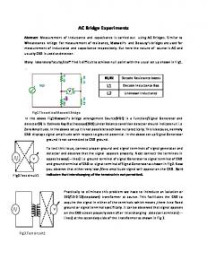
Introduction - Chapter 4: AC CIRCUITS - Volume VI - Experiments
Volume Volume Volume Volume Volume III Volume VI | | | IV - | V - | | Forums | Links | I - DC II - AC Semiconductors Experiments Digital Reference Introduction Transformer -- power supply
Introduction
Build a transformer Variable inductor
All About Circuits > Volume VI - Experiments > Chapter 4: AC CIRCUITS > Introduction
Sensitive audio detector Sensing AC magnetic fields
Introduction
Sensing AC electric fields Automotive alternator Phase shift Sound cancellation Musical keyboard as a signal generator PC Oscilloscope Waveform analysis Inductor-capacitor "tank" circuit
"AC" stands for Alternating Current, which can refer to either voltage or current that alternates in polarity or direction, respectively. These experiments are designed to introduce you to several important concepts specific to AC. A convenient source of AC voltage is household wall-socket power, which presents significant shock hazard. In order to minimize this hazard while taking advantage of the convenience of this source of AC, a small power supply will be the first project, consisting of a transformer that steps the hazardous voltage (110 to 120 volts AC, RMS) down to 12 volts or less. The title of "power supply" is somewhat misleading. This device does not really act as a source or supply of power, but rather as a power converter, to reduce the hazardous voltage of wallsocket power to a much safer level.
Signal coupling Back to Chapter Index
Volume VI - Experiments SEARCH
Check out our new Electronics Forums! Ask questions and help answer others. Check it out!
http://www.allaboutcircuits.com/vol_6/chpt_4/1.html (1 of 2) [5/11/2005 11:58:17 AM]
Forward >
Introduction - Chapter 4: AC CIRCUITS - Volume VI - Experiments All About Electric Circuits. Copyright 2003, AllAboutCircuits.com, All Rights Reserved. Disclaimer. Contact.
http://www.allaboutcircuits.com/vol_6/chpt_4/1.html (2 of 2) [5/11/2005 11:58:17 AM]
All About Circuits :: Volume I - DC
Volume I Volume Volume III | | | - DC II - AC Semiconductors
Volume Volume V - Volume VI IV - | | | Forums | Links | Reference Experiments Digital
Chapter 1: BASIC CONCEPTS OF ELECTRICITY Chapter 2: OHM'S LAW
Volume I - DC All About Circuits > Volume I - DC
Chapter 3: ELECTRICAL SAFETY Chapter 4: SCIENTIFIC NOTATION AND METRIC PREFIXES Chapter 5: SERIES AND PARALLEL CIRCUITS Chapter 6: DIVIDER CIRCUITS AND KIRCHHOFF'S LAWS Chapter 7: SERIESPARALLEL COMBINATION CIRCUITS Chapter 8: DC METERING CIRCUITS Chapter 9: ELECTRICAL INSTRUMENTATION SIGNALS Chapter 10: DC NETWORK ANALYSIS Chapter 11: BATTERIES AND POWER SYSTEMS Chapter 12: THE PHYSICS OF CONDUCTORS AND INSULATORS Chapter 13: CAPACITORS Chapter 14: MAGNETISM AND ELECTROMAGNETISM Chapter 15: INDUCTORS Chapter 16: RC AND L/R TIME CONSTANTS
http://www.allaboutcircuits.com/vol_1/index.html (1 of 2) [5/11/2005 11:58:19 AM]
All About Circuits :: Volume I - DC
Volume I - DC SEARCH
Check out our new Electronics Forums! Ask questions and help answer others. Check it out! All About Electric Circuits. Copyright 2003, AllAboutCircuits.com, All Rights Reserved. Disclaimer. Contact.
http://www.allaboutcircuits.com/vol_1/index.html (2 of 2) [5/11/2005 11:58:19 AM]
All About Circuits :: Volume II - AC
Volume I Volume Volume III | | | - DC II - AC Semiconductors
Volume Volume V - Volume VI IV - | | | Forums | Links | Reference Experiments Digital
Chapter 1: BASIC AC THEORY Chapter 2: COMPLEX NUMBERS
Volume II - AC All About Circuits > Volume II - AC
Chapter 3: REACTANCE AND IMPEDANCE -INDUCTIVE Chapter 4: REACTANCE AND IMPEDANCE -CAPACITIVE Chapter 5: REACTANCE AND IMPEDANCE -- R, L, AND C Chapter 6: RESONANCE Chapter 7: MIXEDFREQUENCY AC SIGNALS Chapter 8: FILTERS Chapter 9: TRANSFORMERS Chapter 10: POLYPHASE AC CIRCUITS Chapter 11: POWER FACTOR Chapter 12: AC METERING CIRCUITS Chapter 13: TRANSMISSION LINES
Volume II - AC SEARCH
Check out our new Electronics Forums! Ask questions and help answer others. Check it out!
http://www.allaboutcircuits.com/vol_2/index.html (1 of 2) [5/11/2005 11:58:21 AM]
All About Circuits :: Volume II - AC
All About Electric Circuits. Copyright 2003, AllAboutCircuits.com, All Rights Reserved. Disclaimer. Contact.
http://www.allaboutcircuits.com/vol_2/index.html (2 of 2) [5/11/2005 11:58:21 AM]
All About Circuits :: Volume III - Semiconductors
Volume I Volume Volume III | | | - DC II - AC Semiconductors
Volume Volume V - Volume VI IV - | | | Forums | Links | Reference Experiments Digital
Chapter 1: AMPLIFIERS AND ACTIVE DEVICES Chapter 2: SOLID-STATE DEVICE THEORY
Volume III - Semiconductors All About Circuits > Volume III - Semiconductors
Chapter 3: DIODES AND RECTIFIERS Chapter 4: BIPOLAR JUNCTION TRANSISTORS Chapter 5: JUNCTION FIELDEFFECT TRANSISTORS Chapter 6: INSULATEDGATE FIELD-EFFECT TRANSISTORS Chapter 7: THYRISTORS Chapter 8: OPERATIONAL AMPLIFIERS Chapter 9: PRACTICAL ANALOG SEMICONDUCTOR CIRCUITS Chapter 10: ACTIVE FILTERS Chapter 11: DC MOTOR DRIVES Chapter 12: INVERTERS AND AC MOTOR DRIVES Chapter 13: ELECTRON TUBES
Volume III - Semiconductors SEARCH
Check out our new Electronics Forums! Ask questions and help answer others. Check it out!
http://www.allaboutcircuits.com/vol_3/index.html (1 of 2) [5/11/2005 11:58:23 AM]
All About Circuits :: Volume III - Semiconductors
All About Electric Circuits. Copyright 2003, AllAboutCircuits.com, All Rights Reserved. Disclaimer. Contact.
http://www.allaboutcircuits.com/vol_3/index.html (2 of 2) [5/11/2005 11:58:23 AM]
All About Circuits :: Volume IV - Digital
Volume I Volume Volume III | | | - DC II - AC Semiconductors
Volume Volume V - Volume VI IV - | | | Forums | Links | Reference Experiments Digital
Chapter 1: NUMERATION SYSTEMS Chapter 2: BINARY ARITHMETIC
Volume IV - Digital All About Circuits > Volume IV - Digital
Chapter 3: LOGIC GATES Chapter 4: SWITCHES Chapter 5: ELECTROMECHANICAL RELAYS Chapter 6: LADDER LOGIC Chapter 7: BOOLEAN ALGEBRA Chapter 8: KARNAUGH MAPPING Chapter 9: COMBINATIONAL LOGIC FUNCTIONS Chapter 10: MULTIVIBRATORS Chapter 11: COUNTERS Chapter 12: SHIFT REGISTERS Chapter 13: DIGITALANALOG CONVERSION Chapter 14: DIGITAL COMMUNICATION Chapter 15: DIGITAL STORAGE (MEMORY) Chapter 16: PRINCIPLES OF DIGITAL COMPUTING
Volume IV - Digital SEARCH
Check out our new Electronics Forums! Ask questions and help answer others. Check it out!
http://www.allaboutcircuits.com/vol_4/index.html (1 of 2) [5/11/2005 11:58:29 AM]
All About Circuits :: Volume IV - Digital
All About Electric Circuits. Copyright 2003, AllAboutCircuits.com, All Rights Reserved. Disclaimer. Contact.
http://www.allaboutcircuits.com/vol_4/index.html (2 of 2) [5/11/2005 11:58:29 AM]
All About Circuits :: Volume V - Reference
Volume I Volume Volume III | | | - DC II - AC Semiconductors
Chapter 1: USEFUL EQUATIONS AND CONVERSION FACTORS Chapter 2: RESISTOR COLOR CODES
Volume Volume V - Volume VI IV - | | | Forums | Links | Reference Experiments Digital
Volume V - Reference All About Circuits > Volume V - Reference
Chapter 3: CONDUCTOR AND INSULATOR TABLES Chapter 4: ALGEBRA REFERENCE Chapter 5: TRIGONOMETRY REFERENCE Chapter 6: CALCULUS REFERENCE Chapter 7: USING THE SPICE CIRCUIT SIMULATION PROGRAM Chapter 8: TROUBLESHOOTING -THEORY AND PRACTICE Chapter 9: CIRCUIT SCHEMATIC SYMBOLS Chapter 10: PERIODIC TABLE OF THE ELEMENTS
Volume V - Reference SEARCH
Check out our new Electronics Forums! Ask questions and help answer others. Check it out!
http://www.allaboutcircuits.com/vol_5/index.html (1 of 2) [5/11/2005 11:58:30 AM]
All About Circuits :: Volume V - Reference
All About Electric Circuits. Copyright 2003, AllAboutCircuits.com, All Rights Reserved. Disclaimer. Contact.
http://www.allaboutcircuits.com/vol_5/index.html (2 of 2) [5/11/2005 11:58:30 AM]
All About Circuits :: Volume VI - Experiments
Volume I Volume Volume III | | | - DC II - AC Semiconductors
Volume Volume V - Volume VI IV - | | | Forums | Links | Reference Experiments Digital
Chapter 1: INTRODUCTION Chapter 2: BASIC CONCEPTS AND TEST EQUIPMENT
Volume VI - Experiments All About Circuits > Volume VI - Experiments
Chapter 3: DC CIRCUITS Chapter 4: AC CIRCUITS Chapter 5: DISCRETE SEMICONDUCTOR CIRCUITS Chapter 6: ANALOG INTEGRATED CIRCUITS Chapter 7: DIGITAL INTEGRATED CIRCUITS
Volume VI - Experiments SEARCH
Check out our new Electronics Forums! Ask questions and help answer others. Check it out!
http://www.allaboutcircuits.com/vol_6/index.html (1 of 2) [5/11/2005 11:58:31 AM]
All About Circuits :: Volume VI - Experiments
All About Electric Circuits. Copyright 2003, AllAboutCircuits.com, All Rights Reserved. Disclaimer. Contact.
http://www.allaboutcircuits.com/vol_6/index.html (2 of 2) [5/11/2005 11:58:31 AM]
All About Circuits :: Useful Links
Volume Volume Volume Volume Volume III Volume VI | | | IV - | V - | | Forums | Links | I - DC II - AC Semiconductors Experiments Digital Reference
Search All Volumes
Links
SEARCH
Here are some other websites that have a lot of great information. If you know of any other links, or if you run a website and would like to swap links, please contact me
Check out our new Electronics Forums! Ask questions and help answer others. Check it out! ● ● ●
Circuits for the Hobbyist Electronics Tutorials Bowden's Hobby Circuits
http://www.allaboutcircuits.com/l_links.html (1 of 2) [5/11/2005 11:58:32 AM]
All About Circuits :: Useful Links
All About Electric Circuits. Copyright 2003, AllAboutCircuits.com, All Rights Reserved. Disclaimer. Contact.
http://www.allaboutcircuits.com/l_links.html (2 of 2) [5/11/2005 11:58:32 AM]
All About Circuits :: Complete guide to Electric Circuits
Volume Volume Volume Volume Volume III Volume VI | | | IV - | V - | | Forums | Links | I - DC II - AC Semiconductors Experiments Digital Reference
Search All Volumes SEARCH
Check out our new Electronics Forums! Ask questions and help answer others. Check it out!
Welcome to AllAboutCircuits.com This site provides a series of online textbooks covering electricity and electronics. The information provided is great for both students and hobbyists who are looking to expand their knowledge in this field. Please keep in mind that the textbooks are not 100% complete. They are a continuous piece of work, and thus will continually be updated. This E-Book was written by Tony R. Kuphaldt. Please visit the contributor's page for a list of major contributors who have generously given their time and knowledge to better this book.
http://www.allaboutcircuits.com/ (1 of 2) [5/11/2005 11:58:32 AM]
All About Circuits :: Complete guide to Electric Circuits
All About Electric Circuits. Copyright 2003, AllAboutCircuits.com, All Rights Reserved. Disclaimer. Contact.
http://www.allaboutcircuits.com/ (2 of 2) [5/11/2005 11:58:32 AM]
All About Circuits :: Contributor's List
Volume Volume Volume Volume Volume III Volume VI | | | IV - | V - | | Forums | Links | I - DC II - AC Semiconductors Experiments Digital Reference
Search All Volumes
Contributor's List
SEARCH
Check out our new Electronics Forums! Ask questions and help answer others. Check it out!
Volume 1 Benjamin Crowell, Ph.D. ● ●
●
Date(s) of contribution(s): January 2001 Nature of contribution: Suggestions on improving technical accuracy of electric field and charge explanations in the first two chapters. Contact at:
[email protected]
Tony R. Kuphaldt ● ● ●
Date(s) of contribution(s): 1996 to present Nature of contribution: Original author. Contact at:
[email protected]
Ron LaPlante ● ●
Date(s) of contribution(s): October 1998 Nature of contribution: Helped create the "table" concept for use in analysis of series and parallel circuits.
Jason Starck ● ●
●
Date(s) of contribution(s): June 2000 Nature of contribution: HTML formatting, some error corrections. Contact at:
[email protected]
Warren Young ● ●
Date(s) of contribution(s): August 2002 Nature of contribution: Provided capacitor photographs for chapter 13.
Volume 2 http://www.allaboutcircuits.com/l_contributors.html (1 of 3) [5/11/2005 11:58:33 AM]
All About Circuits :: Contributor's List
Tony R. Kuphaldt ● ● ●
Date(s) of contribution(s): 1996 to present Nature of contribution: Original author. Contact at:
[email protected]
Jason Starck ● ●
●
Date(s) of contribution(s): May-June 2000 Nature of contribution: HTML formatting, some error corrections. Contact at:
[email protected]
Volume 3 Tony R. Kuphaldt ● ● ●
Date(s) of contribution(s): 1996 to present Nature of contribution: Original author. Contact at:
[email protected]
Warren Young ● ●
Date(s) of contribution(s): August 2002 Nature of contribution: Provided initial text for "Power supply circuits" section of chapter 9.
Volume 4 Tony R. Kuphaldt ● ● ●
Date(s) of contribution(s): 1996 to present Nature of contribution: Original author. Contact at:
[email protected]
Volume 5 Alejandro Gamero Divasto ● ●
Date(s) of contribution(s): January 2002 Nature of contribution: Suggestions related to troubleshooting: caveat regarding swapping two similar components as a troubleshooting tool; avoiding pressure placed on the troubleshooter; perils of "team" troubleshooting; wisdom of recording system history;
http://www.allaboutcircuits.com/l_contributors.html (2 of 3) [5/11/2005 11:58:33 AM]
All About Circuits :: Contributor's List
operator error as a cause of failure; and the perils of fingerpointing.
Tony R. Kuphaldt ● ● ●
Date(s) of contribution(s): 1996 to present Nature of contribution: Original author. Contact at:
[email protected]
Volume 6 Tony R. Kuphaldt ● ● ●
Date(s) of contribution(s): 1996 to present Nature of contribution: Original author. Contact at:
[email protected]
All About Electric Circuits. Copyright 2003, AllAboutCircuits.com, All Rights Reserved. Disclaimer. Contact.
http://www.allaboutcircuits.com/l_contributors.html (3 of 3) [5/11/2005 11:58:33 AM]
All About Circuits :: Dislaimer
Volume Volume Volume Volume Volume III Volume VI | | | IV - | V - | | Forums | Links | I - DC II - AC Semiconductors Experiments Digital Reference
Search All Volumes
Dislaimer
SEARCH
Check out our new Electronics Forums! Ask questions and help answer others. Check it out!
All of the information contained within this website is provided for educational use only. By using this website you agree that you will not hold the owners of this website liable for any event that should happen as a result of you following the information provided within this website. Use the information provided within this website at your own risk. The information within this website is provided asis without warranty of guarantee of any kind. This book is a modified version of the EBook "Lessons In Electric Circuits", which is Copyright © 2000-2003, Tony R. Kuphaldt. The original book is released under the Design Science License, and can be read locally here. More info about it can be found here. In turn, this modified version is also released under the same Design Science License. To read the site's Privacy Policy, please click here.
http://www.allaboutcircuits.com/l_disclaimer.html (1 of 2) [5/11/2005 11:58:34 AM]
All About Circuits :: Dislaimer
All About Electric Circuits. Copyright 2003, AllAboutCircuits.com, All Rights Reserved. Disclaimer. Contact.
http://www.allaboutcircuits.com/l_disclaimer.html (2 of 2) [5/11/2005 11:58:34 AM]
All About Circuits :: DESIGN SCIENCE LICENSE
Volume Volume Volume Volume Volume III Volume VI | | | IV - | V - | | Forums | Links | I - DC II - AC Semiconductors Experiments Digital Reference
Search All Volumes
DESIGN SCIENCE LICENSE
SEARCH
Check out our new Electronics Forums! Ask questions and help answer others. Check it out!
DESIGN SCIENCE LICENSE Copyright © 1999-2000 Michael Stutz
[email protected] Verbatim copying of this document is permitted, in any medium.
0. Preamble Copyright law gives certain exclusive rights to the author of a work, including the rights to copy, modify and distribute the work (the "reproductive," "adaptative," and "distribution" rights). The idea of "copyleft" is to willfully revoke the exclusivity of those rights under certain terms and conditions, so that anyone can copy and distribute the work or properly attributed derivative works, while all copies remain under the same terms and conditions as the original. The intent of this license is to be a general "copyleft" that can be applied to any kind of work that has protection under copyright. This license states those certain conditions under which a work published under its terms may be copied, distributed, and modified. Whereas "design science" is a strategy for the development of artifacts as a way to reform the environment (not people) and subsequently improve the universal standard of living, this Design Science License was written and deployed as a strategy for promoting the progress of science and art through reform of the environment.
1. Definitions "License" shall mean this Design Science License. The License applies to any work which contains a notice placed by the work's copyright holder stating that it is published under the terms of this Design Science License.
http://www.allaboutcircuits.com/l_dcl.html (1 of 5) [5/11/2005 11:58:35 AM]
All About Circuits :: DESIGN SCIENCE LICENSE
"Work" shall mean such an aforementioned work. The License also applies to the output of the Work, only if said output constitutes a "derivative work" of the licensed Work as defined by copyright law. "Object Form" shall mean an executable or performable form of the Work, being an embodiment of the Work in some tangible medium. "Source Data" shall mean the origin of the Object Form, being the entire, machine-readable, preferred form of the Work for copying and for human modification (usually the language, encoding or format in which composed or recorded by the Author); plus any accompanying files, scripts or other data necessary for installation, configuration or compilation of the Work. (Examples of "Source Data" include, but are not limited to, the following: if the Work is an image file composed and edited in 'PNG' format, then the original PNG source file is the Source Data; if the Work is an MPEG 1.0 layer 3 digital audio recording made from a 'WAV' format audio file recording of an analog source, then the original WAV file is the Source Data; if the Work was composed as an unformatted plaintext file, then that file is the the Source Data; if the Work was composed in LaTeX, the LaTeX file(s) and any image files and/or custom macros necessary for compilation constitute the Source Data.) "Author" shall mean the copyright holder(s) of the Work. The individual licensees are referred to as "you."
2. Rights and copyright The Work is copyright the Author. All rights to the Work are reserved by the Author, except as specifically described below. This License describes the terms and conditions under which the Author permits you to copy, distribute and modify copies of the Work. In addition, you may refer to the Work, talk about it, and (as dictated by "fair use") quote from it, just as you would any copyrighted material under copyright law. Your right to operate, perform, read or otherwise interpret and/or execute the Work is unrestricted; however, you do so at your own risk, because the Work comes WITHOUT ANY WARRANTY -- see Section 7 ("NO WARRANTY") below.
3. Copying and distribution Permission is granted to distribute, publish or otherwise present verbatim copies of the entire Source Data of the Work, in any medium, provided that full copyright notice and disclaimer of warranty, where applicable, is conspicuously published on all copies, and a copy of this License is distributed along with the Work. Permission is granted to distribute, publish or otherwise present copies of the Object Form of the Work, in any medium, under the terms for distribution of Source Data above and also provided that one of the following additional
http://www.allaboutcircuits.com/l_dcl.html (2 of 5) [5/11/2005 11:58:35 AM]
All About Circuits :: DESIGN SCIENCE LICENSE
conditions are met: (a) The Source Data is included in the same distribution, distributed under the terms of this License; or (b) A written offer is included with the distribution, valid for at least three years or for as long as the distribution is in print (whichever is longer), with a publiclyaccessible address (such as a URL on the Internet) where, for a charge not greater than transportation and media costs, anyone may receive a copy of the Source Data of the Work distributed according to the section above; or (c) A third party's written offer for obtaining the Source Data at no cost, as described in paragraph (b) above, is included with the distribution. This option is valid only if you are a non-commercial party, and only if you received the Object Form of the Work along with such an offer. You may copy and distribute the Work either gratis or for a fee, and if desired, you may offer warranty protection for the Work. The aggregation of the Work with other works which are not based on the Work -such as but not limited to inclusion in a publication, broadcast, compilation, or other media -- does not bring the other works in the scope of the License; nor does such aggregation void the terms of the License for the Work.
4. Modification Permission is granted to modify or sample from a copy of the Work, producing a derivative work, and to distribute the derivative work under the terms described in the section for distribution above, provided that the following terms are met: (a) The new, derivative work is published under the terms of this License. (b) The derivative work is given a new name, so that its name or title can not be confused with the Work, or with a version of the Work, in any way. (c) Appropriate authorship credit is given: for the differences between the Work and the new derivative work, authorship is attributed to you, while the material sampled or used from the Work remains attributed to the original Author; appropriate notice must be included with the new work indicating the nature and the dates of any modifications of the Work made by you.
5. No restrictions You may not impose any further restrictions on the Work or any of its derivative works beyond those restrictions described in this License.
6. Acceptance Copying, distributing or modifying the Work (including but not limited to http://www.allaboutcircuits.com/l_dcl.html (3 of 5) [5/11/2005 11:58:35 AM]
All About Circuits :: DESIGN SCIENCE LICENSE
sampling from the Work in a new work) indicates acceptance of these terms. If you do not follow the terms of this License, any rights granted to you by the License are null and void. The copying, distribution or modification of the Work outside of the terms described in this License is expressly prohibited by law. If for any reason, conditions are imposed on you that forbid you to fulfill the conditions of this License, you may not copy, distribute or modify the Work at all. If any part of this License is found to be in conflict with the law, that part shall be interpreted in its broadest meaning consistent with the law, and no other parts of the License shall be affected.
7. No warranty THE WORK IS PROVIDED "AS IS," AND COMES WITH ABSOLUTELY NO WARRANTY, EXPRESS OR IMPLIED, TO THE EXTENT PERMITTED BY APPLICABLE LAW, INCLUDING BUT NOT LIMITED TO THE IMPLIED WARRANTIES OF MERCHANTABILITY OR FITNESS FOR A PARTICULAR PURPOSE.
8. Disclaimer of liability IN NO EVENT SHALL THE AUTHOR OR CONTRIBUTORS BE LIABLE FOR ANY DIRECT, INDIRECT, INCIDENTAL, SPECIAL, EXEMPLARY, OR CONSEQUENTIAL DAMAGES (INCLUDING, BUT NOT LIMITED TO, PROCUREMENT OF SUBSTITUTE GOODS OR SERVICES; LOSS OF USE, DATA, OR PROFITS; OR BUSINESS INTERRUPTION) HOWEVER CAUSED AND ON ANY THEORY OF LIABILITY, WHETHER IN CONTRACT, STRICT LIABILITY, OR TORT (INCLUDING NEGLIGENCE OR OTHERWISE) ARISING IN ANY WAY OUT OF THE USE OF THIS WORK, EVEN IF ADVISED OF THE POSSIBILITY OF SUCH DAMAGE.
END OF TERMS AND CONDITIONS
http://www.allaboutcircuits.com/l_dcl.html (4 of 5) [5/11/2005 11:58:35 AM]
All About Circuits :: DESIGN SCIENCE LICENSE
All About Electric Circuits. Copyright 2003, AllAboutCircuits.com, All Rights Reserved. Disclaimer. Contact.
http://www.allaboutcircuits.com/l_dcl.html (5 of 5) [5/11/2005 11:58:35 AM]
All About Circuits :: Contact
Volume Volume Volume Volume Volume III Volume VI | | | IV - | V - | | Forums | Links | I - DC II - AC Semiconductors Experiments Digital Reference Search All Volumes
SEARCH
Check out our new Electronics Forums! Ask questions and help answer others. Check it out!
Contact If you need to contact the webmaster click here
All About Electric Circuits. Copyright 2003, AllAboutCircuits.com, All Rights Reserved. Disclaimer. Contact.
http://www.allaboutcircuits.com/l_contact.html [5/11/2005 11:58:35 AM]
All About Circuits :: Privacy Policy
Volume Volume Volume Volume Volume III Volume VI | | | IV - | V - | | Forums | Links | I - DC II - AC Semiconductors Experiments Digital Reference
Search All Volumes
Privacy Policy
SEARCH
Privacy Policy Statement Check out our new Electronics Forums! Ask questions and help answer others. Check it out!
This is the web site of AllAboutCircuits.com.
We can be reached via e-mail. For each visitor to our Web page, our Web server automatically recognizes only the consumer's domain name, but not the e-mail address (where possible). We collect only the domain name, but not the e-mail address of visitors to our Web page, aggregate information on what pages consumers access or visit. The information we collect is used for internal review and is then discarded, used to improve the content of our Web page, used to customize the content and/or layout of our page for each individual visitor. With respect to cookies: We do not set any cookies. With respect to Ad Servers: We do not partner with or have special relationships with any ad server companies. Upon request we provide site visitors with access to no information that we have collected and that we maintain about them. Upon request we offer visitors no ability to have factual inaccuracies corrected in information that we maintain about them
http://www.allaboutcircuits.com/l_privacypolicy.html (1 of 2) [5/11/2005 11:58:36 AM]
All About Circuits :: Privacy Policy
All About Electric Circuits. Copyright 2003, AllAboutCircuits.com, All Rights Reserved. Disclaimer. Contact.
http://www.allaboutcircuits.com/l_privacypolicy.html (2 of 2) [5/11/2005 11:58:36 AM]
Volume VI - Experiments :: Chapter 1: INTRODUCTION
Volume Volume Volume Volume Volume III Volume VI | | | IV - | V - | | Forums | Links | I - DC II - AC Semiconductors Experiments Digital Reference Electronics as science Setting up a home lab
Volume VI - Experiments
Chapter 1: INTRODUCTION SEARCH
All About Circuits > Volume VI - Experiments > Chapter 1: INTRODUCTION
Check out our new Electronics Forums! Ask questions and help answer others. Check it out!
All About Electric Circuits. Copyright 2003, AllAboutCircuits.com, All Rights Reserved. Disclaimer. Contact.
http://www.allaboutcircuits.com/vol_6/chpt_1/index.html [5/11/2005 11:58:37 AM]
Electronics as science - Chapter 1: INTRODUCTION - Volume VI - Experiments
Volume Volume Volume Volume Volume III Volume VI | | | IV - | V - | | Forums | Links | I - DC II - AC Semiconductors Experiments Digital Reference Electronics as science Setting up a home lab Back to Chapter Index
Electronics as science All About Circuits > Volume VI - Experiments > Chapter 1: INTRODUCTION > Electronics as science
Volume VI - Experiments SEARCH
Check out our new Electronics Forums! Ask questions and help answer others. Check it out!
Electronics as science Electronics is a science, and a very accessible science at that. With other areas of scientific study, expensive equipment is generally required to perform any nontrivial experiments. Not so with electronics. Many advanced concepts may be explored using parts and equipment totaling under a few hundred US dollars. This is good, because hands-on experimentation is vital to gaining scientific knowledge about any subject. When I starting writing Lessons In Electric Circuits, my intent was to create a textbook suitable for introductory college use. However, being mostly self-taught in electronics myself, I knew the value of a good textbook to hobbyists and experimenters not enrolled in any formal electronics course. Many people selflessly volunteered their time and expertise in helping me learn electronics when I was younger, and my intent is to honor their service and love by giving back to the world what they gave to me. In order for someone to teach themselves a science such as electronics, they must engage in hands-on experimentation. Knowledge gleaned from books alone has limited use, especially in scientific endeavors. If my contribution to society is to be complete, I must include a guide to experimentation along with the text(s) on theory, so that the individual learning on their own has a resource to guide their experimental adventures. A formal laboratory course for college electronics study requires an enormous amount of work to prepare, and usually must be based around specific parts and equipment so that the experiments will be sufficient detailed, with results sufficiently precise to allow for rigorous comparison between experimental and theoretical data. A process of assessment, articulated through a qualified instructor, is also vital to guarantee that a certain level of learning has taken place. Peer review (comparison of experimental results with the work of others) is another important component of college-level laboratory study, and helps to improve the quality of learning. Since I cannot meet these criteria through the medium of a book, it is impractical for me to present a complete laboratory course here. In the interest of keeping this experiment guide reasonably low-cost for people to follow, and practical for deployment over the internet, I am forced to design the experiments at a lower level than what would be expected for a college lab course. The experiments in this volume begin at a level appropriate for someone with no
http://www.allaboutcircuits.com/vol_6/chpt_1/1.html (1 of 3) [5/11/2005 11:58:38 AM]
Electronics as science - Chapter 1: INTRODUCTION - Volume VI - Experiments
electronics knowledge, and progress to higher levels. They stress qualitative knowledge over quantitative knowledge, although they could serve as templates for more rigorous coursework. If there is any portion of Lessons In Electric Circuits that will remain "incomplete," it is this one: I fully intend to continue adding experiments ad infinitum so as to provide the experimenter or hobbyist with a wealth of ideas to explore the science of electronics. This volume of the book series is also the easiest to contribute to, for those who would like to help me in providing free information to people learning electronics. It doesn't take a tremendous effort to describe an experiment or two, and I will gladly include it if you email it to me, giving you full credit for the work. Refer to Appendix 2 for details on contributing to this book. When performing these experiments, feel free to explore by trying different circuit construction and measurement techniques. If something isn't working as the text describes it should, don't give up! It's probably due to a simple problem in construction (loose wire, wrong component value) or test equipment setup. It can be frustrating working through these problems on your own, but the knowledge gained by "troubleshooting" a circuit yourself is at least as important as the knowledge gained by a properly functioning experiment. This is one of the most important reasons why experimentation is so vital to your scientific education: the real problems you will invariably encounter in experimentation challenge you to develop practical problem-solving skills. In many of these experiments, I offer part numbers for Radio Shack brand components. This is not an endorsement of Radio Shack, but simply a convenient reference to an electronic supply company well-known in North America. Often times, components of better quality and lower price may be obtained through mail-order companies and other, lesser-known supply houses. I strongly recommend that experimenters obtain some of the more expensive components such as transformers (see the AC chapter) by salvaging them from discarded electrical appliances, both for economic and ecological reasons. All experiments shown in this book are designed with safety in mind. It is nearly impossible to shock or otherwise hurt yourself by battery-powered experiments or other circuits of low voltage. However, hazards do exist building anything with your own two hands. Where there is a greater-than-normal level of danger in an experiment, I take efforts to direct the reader's attention toward it. However, it is unfortunately necessary in this litigious society to disclaim any and all liability for the outcome of any experiment presented here. Neither myself nor any contributors bear responsibility for injuries resulting from the construction or use of any of these projects, from the mis-handling of electricity by the experimenter, or from any other unsafe practices leading to injury. Perform these experiments at your own risk!
http://www.allaboutcircuits.com/vol_6/chpt_1/1.html (2 of 3) [5/11/2005 11:58:38 AM]
Electronics as science - Chapter 1: INTRODUCTION - Volume VI - Experiments
All About Electric Circuits. Copyright 2003, AllAboutCircuits.com, All Rights Reserved. Disclaimer. Contact.
http://www.allaboutcircuits.com/vol_6/chpt_1/1.html (3 of 3) [5/11/2005 11:58:38 AM]
Setting up a home lab - Chapter 1: INTRODUCTION - Volume VI - Experiments
Volume Volume Volume Volume Volume III Volume VI | | | IV - | V - | | Forums | Links | I - DC II - AC Semiconductors Experiments Digital Reference Electronics as science Setting up a home lab
Setting up a home lab
Back to Chapter Index
All About Circuits > Volume VI - Experiments > Chapter 1: INTRODUCTION > Setting up a home lab Volume VI - Experiments SEARCH
Check out our new Electronics Forums! Ask questions and help answer others. Check it out!
Setting up a home lab In order to build the circuits described in this volume, you will need a small work area, as well as a few tools and critical supplies. This section describes the setup of a home electronics laboratory.
Work area A work area should consist of a large workbench, desk, or table (preferably wooden) for performing circuit assembly, with household electrical power (120 volts AC) readily accessible to power soldering equipment, power supplies, and any test equipment. Inexpensive desks intended for computer use function very well for this purpose. Avoid a metal-surface desk, as the electrical conductivity of a metal surface creates both a shock hazard and the very distinct possibility of unintentional "short circuits" developing from circuit components touching the metal tabletop. Vinyl and plastic bench surfaces are to be avoided for their ability to generate and store large static-electric charges, which may damage sensitive electronic components. Also, these materials melt easily when exposed to hot soldering irons and molten solder droplets. If you cannot obtain a wooden-surface workbench, you may turn any form of table or desk into one by laying a piece of plywood on top. If you are reasonably skilled with woodworking tools, you may construct your own desk using plywood and 2x4 boards. The work area should be well-lit and comfortable. I have a small radio set up on my own workbench for listening to music or news as I experiment. My own workbench has a "power strip" receptacle and switch assembly mounted to the underside, into which I plug all 120 volt devices. It is convenient to have a single switch for shutting off all power in case of an accidental short-circuit!
Tools A few tools are required for basic electronics work. Most of these tools are inexpensive and easy to obtain. If you desire to keep the cost as low as possible, you might want to search for them at thrift stores and pawn shops before buying them new. As you can tell from the photographs, some of my own tools are rather old but function well nonetheless. http://www.allaboutcircuits.com/vol_6/chpt_1/2.html (1 of 15) [5/11/2005 11:58:44 AM]
Setting up a home lab - Chapter 1: INTRODUCTION - Volume VI - Experiments
First and foremost in your tool collection is a multimeter. This is an electrical instrument designed to measure voltage, current, resistance, and often other variables as well. Multimeters are manufactured in both digital and analog form. A digital multimeter is preferred for precision work, but analog meters are also useful for gaining an intuitive understanding of instrument sensitivity and range. My own digital multimeter is a Fluke model 27, purchased in 1987: Digital multimeter
Most analog multimeters sold today are quite inexpensive, and not necessarily precision test instruments. I recommend having both digital and analog meter types in your tool collection, spending as little money as possible on the analog multimeter and investing in a good-quality digital multimeter (I highly recommend the Fluke brand). ====================================== A test instrument I have found indispensable in my home work is a sensitive voltage detector, or sensitive audio detector, described in nearly identical experiments in two chapters of this book volume. It is nothing more than a sensitized set of audio headphones, equipped with an attenuator (volume control) and limiting diodes to limit sound intensity from strong signals. Its purpose is to audibly indicate the presence of low-intensity voltage signals, DC or AC. In the absence of an oscilloscope, this is a most valuable tool, because it allows you to listen to an electronic signal, and thereby determine something of its nature. Few tools engender an intuitive comprehension of frequency and amplitude as this! I cite its use in many of the experiments shown in this volume, so I strongly encourage that you build your own. Second only to a multimeter, it is the most useful piece of test equipment in the collection of the budget electronics experimenter. Sensitive voltage/audio detector
http://www.allaboutcircuits.com/vol_6/chpt_1/2.html (2 of 15) [5/11/2005 11:58:44 AM]
Setting up a home lab - Chapter 1: INTRODUCTION - Volume VI - Experiments
As you can see, I built my detector using scrap parts (household electrical switch/receptacle box for the enclosure, section of brown lamp cord for the test leads). Even some of the internal components were salvaged from scrap (the step-down transformer and headphone jack were taken from an old radio, purchased in non-working condition from a thrift store). The entire thing, including the headphones purchased second-hand, cost no more than $15 to build. Of course, one could take much greater care in choosing construction materials (metal box, shielded test probe cable), but it probably wouldn't improve its performance significantly. The single most influential component with regard to detector sensitivity is the headphone assembly: generally speaking, the greater the "dB" rating of the headphones, the better they will function for this purpose. Since the headphones need not be modified for use in the detector circuit, and they can be unplugged from it, you might justify the purchase of more expensive, high-quality headphones by using them as part of a home entertainment (audio/video) system. ====================================== Also essential is a solderless breadboard, sometimes called a prototyping board, or proto-board. This device allows you to quickly join electronic components to one another without having to solder component terminals and wires together. Solderless breadboard
http://www.allaboutcircuits.com/vol_6/chpt_1/2.html (3 of 15) [5/11/2005 11:58:44 AM]
Setting up a home lab - Chapter 1: INTRODUCTION - Volume VI - Experiments
====================================== When working with wire, you need a tool to "strip" the plastic insulation off the ends so that bare copper metal is exposed. This tool is called a wire stripper, and it is a special form of plier with several knife-edged holes in the jaw area sized just right for cutting through the plastic insulation and not the copper, for a multitude of wire sizes, or gauges. Shown here are two different sizes of wire stripping pliers: Wire stripping pliers
http://www.allaboutcircuits.com/vol_6/chpt_1/2.html (4 of 15) [5/11/2005 11:58:44 AM]
Setting up a home lab - Chapter 1: INTRODUCTION - Volume VI - Experiments
====================================== In order to make quick, temporary connections between some electronic components, you need jumper wires with small "alligator-jaw" clips at each end. These may be purchased complete, or assembled from clips and wires. Jumper wires (as sold by Radio Shack)
Jumper wires (home-made)
http://www.allaboutcircuits.com/vol_6/chpt_1/2.html (5 of 15) [5/11/2005 11:58:44 AM]
Setting up a home lab - Chapter 1: INTRODUCTION - Volume VI - Experiments
The home-made jumper wires with large, uninsulated (bare metal) alligator clips are okay to use so long as care is taken to avoid any unintentional contact between the bare clips and any other wires or components. For use in crowded breadboard circuits, jumper wires with insulated (rubber-covered) clips like the jumper shown from Radio Shack are much preferred. ====================================== Needle-nose pliers are designed to grasp small objects, and are especially useful for pushing wires into stubborn breadboard holes. Needle-nose pliers
====================================== No tool set would be complete without screwdrivers, and I recommend a complementary pair (3/16 inch slotted and #2 Phillips) as the starting point for your collection. You may later find it useful to invest in a set of jeweler's screwdrivers for work with very small screws and screw-head adjustments. Screwdrivers
http://www.allaboutcircuits.com/vol_6/chpt_1/2.html (6 of 15) [5/11/2005 11:58:44 AM]
Setting up a home lab - Chapter 1: INTRODUCTION - Volume VI - Experiments
====================================== For projects involving printed-circuit board assembly or repair, a small soldering iron and a spool of "rosin-core" solder are essential tools. I recommend a 25 watt soldering iron, no larger for printed circuit board work, and the thinnest solder you can find. Do not use "acid-core" solder! Acid-core solder is intended for the soldering of copper tubes (plumbing), where a small amount of acid helps to clean the copper of surface impurities and provide a stronger bond. If used for electrical work, the residual acid will cause wires to corrode. Also, you should avoid solder containing the metal lead, opting instead for silver-alloy solder. If you do not already wear glasses, a pair of safety glasses is highly recommended while soldering, to prevent bits of molten solder from accidently landing in your eye should a wire release from the joint during the soldering process and fling bits of solder toward you. Soldering iron and solder ("rosin core")
http://www.allaboutcircuits.com/vol_6/chpt_1/2.html (7 of 15) [5/11/2005 11:58:44 AM]
Setting up a home lab - Chapter 1: INTRODUCTION - Volume VI - Experiments
====================================== Projects requiring the joining of large wires by soldering will necessitate a more powerful heat source than a 25 watt soldering iron. A soldering gun is a practical option. Soldering gun
======================================
http://www.allaboutcircuits.com/vol_6/chpt_1/2.html (8 of 15) [5/11/2005 11:58:44 AM]
Setting up a home lab - Chapter 1: INTRODUCTION - Volume VI - Experiments
Knives, like screwdrivers, are essential tools for all kinds of work. For safety's sake, I recommend a "utility" knife with retracting blade. These knives are also advantageous to have for their ability to accept replacement blades. Utility knife
====================================== Pliers other than the needle-nose type are useful for the assembly and disassembly of electronic device chassis. Two types I recommend are slip-joint and adjustable-joint ("Channel-lock"). Slip-joint pliers
http://www.allaboutcircuits.com/vol_6/chpt_1/2.html (9 of 15) [5/11/2005 11:58:44 AM]
Setting up a home lab - Chapter 1: INTRODUCTION - Volume VI - Experiments
Adjustable-joint pliers
====================================== Drilling may be required for the assembly of large projects. Although power drills work well, I have found that a simple hand-crank drill does a remarkable job drilling through plastic, wood, and most metals. It is certainly safer and quieter than a power drill, and costs quite a bit less. Hand drill
http://www.allaboutcircuits.com/vol_6/chpt_1/2.html (10 of 15) [5/11/2005 11:58:44 AM]
Setting up a home lab - Chapter 1: INTRODUCTION - Volume VI - Experiments
As the wear on my drill indicates, it is an often-used tool around my home! ====================================== Some experiments will require a source of audio-frequency voltage signals. Normally, this type of signal is generated in an electronics laboratory by a device called a signal generator or function generator. While building such a device is not impossible (nor difficult!), it often requires the use of an oscilloscope to finetune, and oscilloscopes are usually outside the budgetary range of the home experimenter. A relatively inexpensive alternative to a commercial signal generator is an electronic keyboard of the musical type. You need not be a musician to operate one for the purposes of generating an audio signal (just press any key on the board!), and they may be obtained quite readily at secondhand stores for substantially less than new price. The electronic signal generated by the keyboard is conducted to your circuit via a headphone cable plugged into the "headphones" jack. More details regarding the use of a "Musical Keyboard as a Signal Generator" may be found in the experiment of that name in chapter 4 (AC).
Supplies Wire used in solderless breadboards must be 22-gauge, solid copper. Spools of this wire are available from electronic supply stores and some hardware stores, in different insulation colors. Insulation color has no bearing on the wire's performance, but different colors are sometimes useful for "color-coding" wire functions in a complex circuit. Spool of 22-gauge, solid copper wire
http://www.allaboutcircuits.com/vol_6/chpt_1/2.html (11 of 15) [5/11/2005 11:58:44 AM]
Setting up a home lab - Chapter 1: INTRODUCTION - Volume VI - Experiments
Note how the last 1/4 inch or so of the copper wire protruding from the spool has been "stripped" of its plastic insulation. ====================================== An alternative to solderless breadboard circuit construction is wire-wrap, where 30-gauge (very thin!) solid copper wire is tightly wrapped around the terminals of components inserted through the holes of a fiberglass board. No soldering is required, and the connections made are at least as durable as soldered connections, perhaps more. Wire-wrapping requires a spool of this very thin wire, and a special wrapping tool, the simplest kind resembling a small screwdriver. Wire-wrap wire and wrapping tool
http://www.allaboutcircuits.com/vol_6/chpt_1/2.html (12 of 15) [5/11/2005 11:58:44 AM]
Setting up a home lab - Chapter 1: INTRODUCTION - Volume VI - Experiments
====================================== Large wire (14 gauge and bigger) may be needed for building circuits that carry significant levels of current. Though electrical wire of practically any gauge may be purchased on spools, I have found a very inexpensive source of stranded (flexible), copper wire, available at any hardware store: cheap extension cords. Typically comprised of three wires colored white, black, and green, extension cords are often sold at prices less than the retail cost of the constituent wire alone. This is especially true if the cord is purchased on sale! Also, an extension cord provides you with a pair of 120 volt connectors: male (plug) and female (receptacle) that may be used for projects powered by 120 volts. Extension cord, in package
http://www.allaboutcircuits.com/vol_6/chpt_1/2.html (13 of 15) [5/11/2005 11:58:44 AM]
Setting up a home lab - Chapter 1: INTRODUCTION - Volume VI - Experiments
To extract the wires, carefully cut the outer layer of plastic insulation away using a utility knife. With practice, you may find you can peel away the outer insulation by making a short cut in it at one end of the cable, then grasping the wires with one hand and the insulation with the other and pulling them apart. This is, of course, much preferable to slicing the entire length of the insulation with a knife, both for safety's sake and for the sake of avoiding cuts in the individual wires' insulation. ====================================== During the course of building many circuits, you will accumulate a large number of small components. One technique for keeping these components organized is to keep them in a plastic "organizer" box like the type used for fishing tackle. Component box
http://www.allaboutcircuits.com/vol_6/chpt_1/2.html (14 of 15) [5/11/2005 11:58:44 AM]
Setting up a home lab - Chapter 1: INTRODUCTION - Volume VI - Experiments
In this view of one of my component boxes, you can see plenty of 1/8 watt resistors, transistors, diodes, and even a few 8-pin integrated circuits ("chips"). Labels for each compartment were made with a permanent ink marker.
< Back
All About Electric Circuits. Copyright 2003, AllAboutCircuits.com, All Rights Reserved. Disclaimer. Contact.
http://www.allaboutcircuits.com/vol_6/chpt_1/2.html (15 of 15) [5/11/2005 11:58:44 AM]
Volume VI - Experiments :: Chapter 2: BASIC CONCEPTS AND TEST EQUIPMENT
Volume Volume Volume Volume Volume III Volume VI | | | IV - | V - | | Forums | Links | I - DC II - AC Semiconductors Experiments Digital Reference Voltmeter usage Ohmmeter usage
Chapter 2: BASIC CONCEPTS AND TEST EQUIPMENT
A very simple circuit
All About Circuits > Volume VI - Experiments > Chapter 2: BASIC CONCEPTS AND TEST EQUIPMENT
Ammeter usage Ohm's Law Nonlinear resistance Power dissipation Circuit with a switch Electromagnetism
Volume VI - Experiments SEARCH
Check out our new Electronics Forums! Ask questions and help answer others. Check it out!
All About Electric Circuits. Copyright 2003, AllAboutCircuits.com, All Rights Reserved. Disclaimer. Contact.
http://www.allaboutcircuits.com/vol_6/chpt_2/index.html [5/11/2005 11:58:45 AM]
Voltmeter usage - Chapter 2: BASIC CONCEPTS AND TEST EQUIPMENT - Volume VI - Experiments
Volume Volume Volume Volume Volume III Volume VI | | | IV - | V - | | Forums | Links | I - DC II - AC Semiconductors Experiments Digital Reference Voltmeter usage Ohmmeter usage
Voltmeter usage
A very simple circuit Ammeter usage
All About Circuits > Volume VI - Experiments > Chapter 2: BASIC CONCEPTS AND TEST EQUIPMENT > Voltmeter usage
Ohm's Law Nonlinear resistance
Voltmeter usage
Power dissipation Circuit with a switch
PARTS AND MATERIALS
Electromagnetism Back to Chapter Index
● ● ● ●
Volume VI - Experiments SEARCH
Check out our new Electronics Forums! Ask questions and help answer others. Check it out!
●
Multimeter, digital or analog Assorted batteries One light-emitting diode (Radio Shack catalog # 276-026 or equivalent) Small "hobby" motor, permanent-magnet type (Radio Shack catalog # 273-223 or equivalent) Two jumper wires with "alligator clip" ends (Radio Shack catalog # 2781156, 278-1157, or equivalent)
A multimeter is an electrical instrument capable of measuring voltage, current, and resistance. Digital multimeters have numerical displays, like digital clocks, for indicating the quantity of voltage, current, or resistance. Analog multimeters indicate these quantities by means of a moving pointer over a printed scale. Analog multimeters tend to be less expensive than digital multimeters, and more beneficial as learning tools for the first-time student of electricity. I strongly recommend purchasing an analog multimeter before purchasing a digital multimeter, but to eventually have both in your tool kit for these experiments.
CROSS-REFERENCES Lessons In Electric Circuits, Volume 1, chapter 1: "Basic Concepts of Electricity" Lessons In Electric Circuits, Volume 1, chapter 8: "DC Metering Circuits"
LEARNING OBJECTIVES ● ● ●
How to measure voltage Characteristics of voltage: existing between two points Selection of proper meter range
http://www.allaboutcircuits.com/vol_6/chpt_2/1.html (1 of 4) [5/11/2005 11:58:47 AM]
Voltmeter usage - Chapter 2: BASIC CONCEPTS AND TEST EQUIPMENT - Volume VI - Experiments
ILLUSTRATION
INSTRUCTIONS In all the experiments in this book, you will be using some sort of test equipment to measure aspects of electricity you cannot directly see, feel, hear, taste, or smell. Electricity -- at least in small, safe quantities -- is insensible by our human bodies. Your most fundamental "eyes" in the world of electricity and electronics will be a device called a multimeter. Multimeters indicate the presence of, and measure the quantity of, electrical properties such as voltage, current, and resistance. In this experiment, you will familiarize yourself with the measurement of voltage. Voltage is the measure of electrical "push" ready to motivate electrons to move through a conductor. In scientific terms, it is the specific energy per unit charge, mathematically defined as joules per coulomb. It is analogous to pressure in a fluid system: the force that moves fluid through a pipe, and is measured in the unit of the Volt (V). Your multimeter should come with some basic instructions. Read them well! If your multimeter is digital, it will require a small battery to operate. If it is analog, it does not need a battery to measure voltage. Some digital multimeters are autoranging. An autoranging meter has only a few selector switch (dial) positions. Manual-ranging meters have several different selector positions for each basic quantity: several for voltage, several for current, and several for resistance. Autoranging is usually found on only the more expensive digital meters, and is to manual ranging as an automatic transmission is to a manual transmission in a car. An autoranging meter "shifts gears" automatically to find the best measurement range to display the particular quantity being measured. Set your multimeter's selector switch to the highest-value "DC volt" position available. Autoranging multimeters may only have a single position for DC voltage, in which case you need to set the switch to that one position. Touch the red test probe to the positive (+) side of a battery, and the black test probe to the negative (-) side of the same battery. The meter should now provide you with some sort of indication. Reverse the test probe connections to the battery if the meter's indication is negative (on an analog meter, a negative value is indicated by the pointer deflecting left instead of right). If your meter is a manual-range type, and the selector switch has been set to a high-range position, the indication will be small. Move the selector switch to the next lower DC voltage range setting and reconnect to the battery. The indication should be stronger now, as indicated by a greater deflection of the analog meter pointer (needle), or more active digits on the digital meter display. For the best
http://www.allaboutcircuits.com/vol_6/chpt_2/1.html (2 of 4) [5/11/2005 11:58:47 AM]
Voltmeter usage - Chapter 2: BASIC CONCEPTS AND TEST EQUIPMENT - Volume VI - Experiments
results, move the selector switch to the lowest-range setting that does not "overrange" the meter. An over-ranged analog meter is said to be "pegged," as the needle will be forced all the way to the right-hand side of the scale, past the fullrange scale value. An over-ranged digital meter sometimes displays the letters "OL", or a series of dashed lines. This indication is manufacturer-specific. What happens if you only touch one meter test probe to one end of a battery? How does the meter have to connect to the battery in order to provide an indication? What does this tell us about voltmeter use and the nature of voltage? Is there such a thing as voltage "at" a single point? Be sure to measure more than one size of battery, and learn how to select the best voltage range on the multimeter to give you maximum indication without over-ranging. Now switch your multimeter to the lowest DC voltage range available, and touch the meter's test probes to the terminals (wire leads) of the light-emitting diode (LED). An LED is designed to produce light when powered by a small amount of electricity, but LEDs also happen to generate DC voltage when exposed to light, somewhat like a solar cell. Point the LED toward a bright source of light with your multimeter connected to it, and note the meter's indication:
Batteries develop electrical voltage through chemical reactions. When a battery "dies," it has exhausted its original store of chemical "fuel." The LED, however, does not rely on an internal "fuel" to generate voltage; rather, it converts optical energy into electrical energy. So long as there is light to illuminate the LED, it will produce voltage. Another source of voltage through energy conversion a generator. The small electric motor specified in the "Parts and Materials" list functions as an electrical generator if its shaft is turned by a mechanical force. Connect your voltmeter (your multimeter, set to the "volt" function) to the motor's terminals just as you connected it to the LED's terminals, and spin the shaft with your fingers. The meter should indicate voltage by means of needle deflection (analog) or numerical readout (digital). If you find it difficult to maintain both meter test probes in connection with the motor's terminals while simultaneously spinning the shaft with your fingers, you may use alligator clip "jumper" wires like this:
Determine the relationship between voltage and generator shaft speed? Reverse the generator's direction of rotation and note the change in meter indication. When you reverse shaft rotation, you change the polarity of the voltage created by the generator. The voltmeter indicates polarity by direction of needle direction (analog) or sign of numerical indication (digital). When the red test lead is positive (+) and the black test lead negative (-), the meter will register voltage in the normal direction. If the applied voltage is of the reverse polarity (negative on red and positive on black), the meter will indicate "backwards."
Forward >
http://www.allaboutcircuits.com/vol_6/chpt_2/1.html (3 of 4) [5/11/2005 11:58:47 AM]
Voltmeter usage - Chapter 2: BASIC CONCEPTS AND TEST EQUIPMENT - Volume VI - Experiments
All About Electric Circuits. Copyright 2003, AllAboutCircuits.com, All Rights Reserved. Disclaimer. Contact.
http://www.allaboutcircuits.com/vol_6/chpt_2/1.html (4 of 4) [5/11/2005 11:58:47 AM]
Ohmmeter usage - Chapter 2: BASIC CONCEPTS AND TEST EQUIPMENT - Volume VI - Experiments
Volume Volume Volume Volume Volume III Volume VI | | | IV - | V - | | Forums | Links | I - DC II - AC Semiconductors Experiments Digital Reference Voltmeter usage Ohmmeter usage
Ohmmeter usage
A very simple circuit Ammeter usage
All About Circuits > Volume VI - Experiments > Chapter 2: BASIC CONCEPTS AND TEST EQUIPMENT > Ohmmeter usage
Ohm's Law Nonlinear resistance
Ohmmeter usage
Power dissipation Circuit with a switch
PARTS AND MATERIALS
Electromagnetism Back to Chapter Index
● ●
●
Volume VI - Experiments SEARCH
● ● ● ● ●
Check out our new Electronics Forums! Ask questions and help answer others. Check it out!
● ●
Multimeter, digital or analog Assorted resistors (Radio Shack catalog # 271-312 is a 500-piece assortment) Rectifying diode (1N4001 or equivalent; Radio Shack catalog # 276-1101) Cadmium Sulphide photocell (Radio Shack catalog # 276-1657) Breadboard (Radio Shack catalog # 276-174 or equivalent) Jumper wires Paper Pencil Glass of water Table salt
This experiment describes how to measure the electrical resistance of several objects. You need not possess all items listed above in order to effectively learn about resistance. Conversely, you need not limit your experiments to these items. However, be sure to never measure the resistance of any electrically "live" object or circuit. In other words, do not attempt to measure the resistance of a battery or any other source of substantial voltage using a multimeter set to the resistance ("ohms") function. Failing to heed this warning will likely result in meter damage and even personal injury.
CROSS-REFERENCES Lessons In Electric Circuits, Volume 1, chapter 1: "Basic Concepts of Electricity" Lessons In Electric Circuits, Volume 1, chapter 8: "DC Metering Circuits"
LEARNING OBJECTIVES
http://www.allaboutcircuits.com/vol_6/chpt_2/2.html (1 of 5) [5/11/2005 11:58:48 AM]
Ohmmeter usage - Chapter 2: BASIC CONCEPTS AND TEST EQUIPMENT - Volume VI - Experiments ● ● ● ● ● ●
Determination and comprehension of "electrical continuity" Determination and comprehension of "electrically common points" How to measure resistance Characteristics of resistance: existing between two points Selection of proper meter range Relative conductivity of various components and materials
ILLUSTRATION
INSTRUCTIONS Resistance is the measure of electrical "friction" as electrons move through a conductor. It is measured in the unit of the "Ohm," that unit symbolized by the capital Greek letter omega (Ω). Set your multimeter to the highest resistance range available. The resistance function is usually denoted by the unit symbol for resistance: the Greek letter omega (Ω), or sometimes by the word "ohms." Touch the two test probes of your meter together. When you do, the meter should register 0 ohms of resistance. If you are using an analog meter, you will notice the needle deflect full-scale when the probes are touched together, and return to its resting position when the probes are pulled apart. The resistance scale on an analog multimeter is reverseprinted from the other scales: zero resistance in indicated at the far right-hand side of the scale, and infinite resistance is indicated at the far left-hand side. There should also be a small adjustment knob or "wheel" on the analog multimeter to calibrate it for "zero" ohms of resistance. Touch the test probes together and move this adjustment until the needle exactly points to zero at the right-hand end of the scale. Although your multimeter is capable of providing quantitative values of measured resistance, it is also useful for qualitative tests of continuity: whether or not there is a continuous electrical connection from one point to another. You can, for instance, test the continuity of a piece of wire by connecting the meter probes to opposite ends of the wire and checking to see the the needle moves full-scale. What would we say about a piece of wire if the ohmmeter needle didn't move at all when the probes were connected to opposite ends? Digital multimeters set to the "resistance" mode indicate non-continuity by displaying some non-numerical indication on the display. Some models say "OL" (Open-Loop), while others display dashed lines. Use your meter to determine continuity between the holes on a breadboard: a device used for temporary construction of circuits, where component terminals are inserted into holes on a plastic grid, metal spring clips underneath each hole connecting certain holes to others. Use small pieces of 22-gauge solid copper wire, inserted into the holes of the breadboard, to connect the meter to these spring clips so that you can test for continuity:
http://www.allaboutcircuits.com/vol_6/chpt_2/2.html (2 of 5) [5/11/2005 11:58:48 AM]
Ohmmeter usage - Chapter 2: BASIC CONCEPTS AND TEST EQUIPMENT - Volume VI - Experiments
An important concept in electricity, closely related to electrical continuity, is that of points being electrically common to each other. Electrically common points are points of contact on a device or in a circuit that have negligible (extremely small) resistance between them. We could say, then, that points within a breadboard column (vertical in the illustrations) are electrically common to each other, because there is electrical continuity between them. Conversely, breadboard points within a row (horizontal in the illustrations) are not electrically common, because there is no continuity between them. Continuity describes what is between points of contact, while commonality describes how the points themselves relate to each other. Like continuity, commonality is a qualitative assessment, based on a relative comparison of resistance between other points in a circuit. It is an important concept to grasp, because there are certain facts regarding voltage in relation to electrically common points that are valuable in circuit analysis and troubleshooting, the first one being that there will never be substantial voltage dropped between points that are electrically common to each other. Select a 10,000 ohm (10 kΩ) resistor from your parts assortment. This resistance value is indicated by a series of color bands: Brown, Black, Orange, and then another color representing the precision of the resistor, Gold (+/- 5%) or Silver (+/- 10%). Some resistors have no color for precision, which marks them as +/- 20%. Other resistors use five color bands to denote their value and precision, in which case the colors for a 10 kΩ resistor will be Brown, Black, Black, Red, and a fifth color for precision. Connect the meter's test probes across the resistor as such, and note its indication on the resistance scale:
If the needle points very close to zero, you need to select a lower resistance range on the meter, just as you needed to select an appropriate voltage range when reading the voltage of a battery. If you are using a digital multimeter, you should see a numerical figure close to 10 shown on the display, with a small "k" symbol on the right-hand side denoting the metric prefix for "kilo" (thousand). Some digital meters are manually-ranged, and require appropriate range selection just as the analog meter. If yours is like this, experiment with different range switch positions and see which one gives you the best indication. Try reversing the test probe connections on the resistor. Does this change the meter's indication at all? What does this tell us about the resistance of a resistor? What happens when you only touch one probe to the resistor? What does this tell us about the nature of resistance, and how it is measured? How does this compare with voltage measurement, and what happened when we tried to measure battery voltage by touching only one probe to the battery? When you touch the meter probes to the resistor terminals, try not to touch both probe tips to your fingers. If you do, you will be measuring the parallel combination of the resistor and your own body, which will tend to make the meter indication lower than it should be! When measuring a 10 kΩ resistor, this error will be minimal, but it may be more severe when measuring other values of resistor. You may safely measure the resistance of your own body by holding one probe tip with the fingers of one hand, and the other probe tip with the fingers of the http://www.allaboutcircuits.com/vol_6/chpt_2/2.html (3 of 5) [5/11/2005 11:58:48 AM]
Ohmmeter usage - Chapter 2: BASIC CONCEPTS AND TEST EQUIPMENT - Volume VI - Experiments
other hand. Note: be very careful with the probes, as they are often sharpened to a needle-point. Hold the probe tips along their length, not at the very points! You may need to adjust the meter range again after measuring the 10 kΩ resistor, as your body resistance tends to be greater than 10,000 ohms hand-tohand. Try wetting your fingers with water and re-measuring resistance with the meter. What impact does this have on the indication? Try wetting your fingers with saltwater prepared using the glass of water and table salt, and remeasuring resistance. What impact does this have on your body's resistance as measured by the meter? Resistance is the measure of friction to electron flow through an object. The less resistance there is between two points, the harder it is for electrons to move (flow) between those two points. Given that electric shock is caused by a large flow of electrons through a person's body, and increased body resistance acts as a safeguard by making it more difficult for electrons to flow through us, what can we ascertain about electrical safety from the resistance readings obtained with wet fingers? Does water increase or decrease shock hazard to people? Measure the resistance of a rectifying diode with an analog meter. Try reversing the test probe connections to the diode and re-measure resistance. What strikes you as being remarkable about the diode, especially in contrast to the resistor? Take a piece of paper and draw a very heavy black mark on it with a pencil (not a pen!). Measure resistance on the black strip with your meter, placing the probe tips at each end of the mark like this:
Move the probe tips closer together on the black mark and note the change in resistance value. Does it increase or decrease with decreased probe spacing? If the results are inconsistent, you need to redraw the mark with more and heavier pencil strokes, so that it is consistent in its density. What does this teach you about resistance versus length of a conductive material? Connect your meter to the terminals of a cadmium-sulphide (CdS) photocell and measure the change in resistance created by differences in light exposure. Just as with the light-emitting diode (LED) of the voltmeter experiment, you may want to use alligator-clip jumper wires to make connection with the component, leaving your hands free to hold the photocell to a light source and/or change meter ranges:
Experiment with measuring the resistance of several different types of materials, just be sure not to try measure anything that produces substantial voltage, like a battery. Suggestions for materials to measure are: fabric, plastic, wood, metal, clean water, dirty water, salt water, glass, diamond (on a diamond ring or other piece of jewelry), paper, rubber, and oil.
< Back Forward >
http://www.allaboutcircuits.com/vol_6/chpt_2/2.html (4 of 5) [5/11/2005 11:58:48 AM]
Ohmmeter usage - Chapter 2: BASIC CONCEPTS AND TEST EQUIPMENT - Volume VI - Experiments
All About Electric Circuits. Copyright 2003, AllAboutCircuits.com, All Rights Reserved. Disclaimer. Contact.
http://www.allaboutcircuits.com/vol_6/chpt_2/2.html (5 of 5) [5/11/2005 11:58:48 AM]
A very simple circuit - Chapter 2: BASIC CONCEPTS AND TEST EQUIPMENT - Volume VI - Experiments
Volume Volume Volume Volume Volume III Volume VI | | | IV - | V - | | Forums | Links | I - DC II - AC Semiconductors Experiments Digital Reference Voltmeter usage Ohmmeter usage
A very simple circuit
A very simple circuit Ammeter usage
All About Circuits > Volume VI - Experiments > Chapter 2: BASIC CONCEPTS AND TEST EQUIPMENT > A very simple circuit
Ohm's Law Nonlinear resistance
A very simple circuit
Power dissipation Circuit with a switch
PARTS AND MATERIALS
Electromagnetism Back to Chapter Index
● ● ● ●
Volume VI - Experiments SEARCH
Check out our new Electronics Forums! Ask questions and help answer others. Check it out!
●
6-volt battery 6-volt incandescent lamp Jumper wires Breadboard Terminal strip
From this experiment on, a multimeter is assumed to be necessary and will not be included in the required list of parts and materials. In all subsequent illustrations, a digital multimeter will be shown instead of an analog meter unless there is some particular reason to use an analog meter. You are encouraged to use both types of meters to gain familiarity with the operation of each in these experiments.
CROSS-REFERENCES Lessons In Electric Circuits, Volume 1, chapter 1: "Basic Concepts of Electricity"
LEARNING OBJECTIVES ● ● ● ● ● ●
Essential configuration needed to make a circuit Normal voltage drops in an operating circuit Importance of continuity to a circuit Working definitions of "open" and "short" circuits Breadboard usage Terminal strip usage
http://www.allaboutcircuits.com/vol_6/chpt_2/3.html (1 of 4) [5/11/2005 11:58:53 AM]
A very simple circuit - Chapter 2: BASIC CONCEPTS AND TEST EQUIPMENT - Volume VI - Experiments
SCHEMATIC DIAGRAM
ILLUSTRATION
INSTRUCTIONS This is the simplest complete circuit in this collection of experiments: a battery and an incandescent lamp. Connect the lamp to the battery as shown in the illustration, and the lamp should light, assuming the battery and lamp are both in good condition and they are matched to one another in terms of voltage. If there is a "break" (discontinuity) anywhere in the circuit, the lamp will fail to light. It does not matter where such a break occurs! Many students assume that because electrons leave the negative (-) side of the battery and continue through the circuit to the positive (+) side, that the wire connecting the negative terminal of the battery to the lamp is more important to circuit operation than the other wire providing a return path for electrons back to the battery. This is not true!
Using your multimeter set to the appropriate "DC volt" range, measure voltage across the battery, across the lamp, and across each jumper wire. Familiarize yourself with the normal voltages in a functioning circuit. Now, "break" the circuit at one point and re-measure voltage between the same sets of points, additionally measuring voltage across the break like this:
What voltages measure the same as before? What voltages are different since introducing the break? How much voltage is manifest, or dropped across the break? What is the polarity of the voltage drop across the break, as indicated by the meter? http://www.allaboutcircuits.com/vol_6/chpt_2/3.html (2 of 4) [5/11/2005 11:58:53 AM]
A very simple circuit - Chapter 2: BASIC CONCEPTS AND TEST EQUIPMENT - Volume VI - Experiments
Re-connect the jumper wire to the lamp, and break the circuit in another place. Measure all voltage "drops" again, familiarizing yourself with the voltages of an "open" circuit. Construct the same circuit on a breadboard, taking care to place the lamp and wires into the breadboard in such a way that continuity will be maintained. The example shown here is only that: an example, not the only way to build a circuit on a breadboard:
Experiment with different configurations on the breadboard, plugging the lamp into different holes. If you encounter a situation where the lamp refuses to light up and the connecting wires are getting warm, you probably have a situation known as a short circuit, where a lower-resistance path than the lamp bypasses current around the lamp, preventing enough voltage from being dropped across the lamp to light it up. Here is an example of a short circuit made on a breadboard:
Here is an example of an accidental short circuit of the type typically made by students unfamiliar with breadboard usage:
Here there is no "shorting" wire present on the breadboard, yet there is a short circuit, and the lamp refuses to light. Based on your understanding of breadboard hole connections, can you determine where the "short" is in this circuit? Short circuits are generally to be avoided, as they result in very high rates of electron flow, causing wires to heat up and battery power sources to deplete. If the power source is substantial enough, a short circuit may cause heat of explosive proportions to manifest, causing equipment damage and hazard to nearby personnel. This is what happens when a tree limb "shorts" across wires on a power line: the limb -- being composed of wet wood -- acts as a lowresistance path to electric current, resulting in heat and sparks. You may also build the battery/lamp circuit on a terminal strip: a length of insulating material with metal bars and screws to attach wires and component terminals to. Here is an example of how this circuit might be constructed on a terminal strip:
< Back Forward >
http://www.allaboutcircuits.com/vol_6/chpt_2/3.html (3 of 4) [5/11/2005 11:58:53 AM]
A very simple circuit - Chapter 2: BASIC CONCEPTS AND TEST EQUIPMENT - Volume VI - Experiments
All About Electric Circuits. Copyright 2003, AllAboutCircuits.com, All Rights Reserved. Disclaimer. Contact.
http://www.allaboutcircuits.com/vol_6/chpt_2/3.html (4 of 4) [5/11/2005 11:58:53 AM]
Ammeter usage - Chapter 2: BASIC CONCEPTS AND TEST EQUIPMENT - Volume VI - Experiments
Volume Volume Volume Volume Volume III Volume VI | | | IV - | V - | | Forums | Links | I - DC II - AC Semiconductors Experiments Digital Reference Voltmeter usage Ohmmeter usage
Ammeter usage
A very simple circuit Ammeter usage
All About Circuits > Volume VI - Experiments > Chapter 2: BASIC CONCEPTS AND TEST EQUIPMENT > Ammeter usage
Ohm's Law Nonlinear resistance
Ammeter usage
Power dissipation Circuit with a switch
PARTS AND MATERIALS
Electromagnetism Back to Chapter Index
● ●
Volume VI - Experiments SEARCH
Check out our new Electronics Forums! Ask questions and help answer others. Check it out!
6-volt battery 6-volt incandescent lamp
Basic circuit construction components such as breadboard, terminal strip, and jumper wires are also assumed to be available from now on, leaving only components and materials unique to the project listed under "Parts and Materials."
CROSS-REFERENCES Lessons In Electric Circuits, Volume 1, chapter 1: "Basic Concepts of Electricity" Lessons In Electric Circuits, Volume 1, chapter 8: "DC Metering Circuits"
LEARNING OBJECTIVES ● ● ●
How to measure current with a multimeter How to check a multimeter's internal fuse Selection of proper meter range
SCHEMATIC DIAGRAM
http://www.allaboutcircuits.com/vol_6/chpt_2/4.html (1 of 4) [5/11/2005 11:58:54 AM]
Ammeter usage - Chapter 2: BASIC CONCEPTS AND TEST EQUIPMENT - Volume VI - Experiments
ILLUSTRATION
INSTRUCTIONS Current is the measure of the rate of electron "flow" in a circuit. It is measured in the unit of the Ampere, simply called "Amp," (A). The most common way to measure current in a circuit is to break the circuit open and insert an "ammeter" in series (in-line) with the circuit so that all electrons flowing through the circuit also have to go through the meter. Because measuring current in this manner requires the meter be made part of the circuit, it is a more difficult type of measurement to make than either voltage or resistance. Some digital meters, like the unit shown in the illustration, have a separate jack to insert the red test lead plug when measuring current. Other meters, like most inexpensive analog meters, use the same jacks for measuring voltage, resistance, and current. Consult your owner's manual on the particular model of meter you own for details on measuring current. When an ammeter is placed in series with a circuit, it ideally drops no voltage as current goes through it. In other words, it acts very much like a piece of wire, with very little resistance from one test probe to the other. Consequently, an ammeter will act as a short circuit if placed in parallel (across the terminals of) a substantial source of voltage. If this is done, a surge in current will result, potentially damaging the meter:
Ammeters are generally protected from excessive current by means of a small fuse located inside the meter housing. If the ammeter is accidently connected across a substantial voltage source, the resultant surge in current will "blow" the fuse and render the meter incapable of measuring current until the fuse is replaced. Be very careful to avoid this scenario! You may test the condition of a multimeter's fuse by switching it to the resistance mode and measuring continuity through the test leads (and through the fuse). On a meter where the same test lead jacks are used for both resistance and current measurement, simply leave the test lead plugs where they are and touch the two probes together. On a meter where different jacks are used, this is how you insert the test lead plugs to check the fuse:
Build the one-battery, one-lamp circuit using jumper wires to connect the battery to the lamp, and verify that the lamp lights up before connecting the meter in series with it. Then, break the circuit open at any point and connect the meter's test probes to the two points of the break to measure current. As usual, if your meter is manually-ranged, begin by selecting the highest range for current, then move the selector switch to lower range positions until the strongest indication is obtained on the meter display without over-ranging it. If the meter indication is "backwards," (left motion on analog needle, or negative reading on a digital display), then reverse the test probe connections and try again. When the http://www.allaboutcircuits.com/vol_6/chpt_2/4.html (2 of 4) [5/11/2005 11:58:54 AM]
Ammeter usage - Chapter 2: BASIC CONCEPTS AND TEST EQUIPMENT - Volume VI - Experiments
ammeter indicates a normal reading (not "backwards"), electrons are entering the black test lead and exiting the red. This is how you determine direction of current using a meter. For a 6-volt battery and a small lamp, the circuit current will be in the range of thousandths of an amp, or milliamps. Digital meters often show a small letter "m" in the right-hand side of the display to indicate this metric prefix. Try breaking the circuit at some other point and inserting the meter there instead. What do you notice about the amount of current measured? Why do you think this is? Re-construct the circuit on a breadboard like this:
Students often get confused when connecting an ammeter to a breadboard circuit. How can the meter be connected so as to intercept all the circuit's current and not create a short circuit? One easy method that guarantees success is this: ●
●
●
●
Identify what wire or component terminal you wish to measure current through. Pull that wire or terminal out of the breadboard hole. Leave it hanging in mid-air. Insert a spare piece of wire into the hole you just pulled the other wire or terminal out of. Leave the other end of this wire hanging in mid-air. Connect the ammeter between the two unconnected wire ends (the two that were hanging in mid-air). You are now assured of measuring current through the wire or terminal initially identified.
Again, measure current through different wires in this circuit, following the same connection procedure outlined above. What do you notice about these current measurements? The results in the breadboard circuit should be the same as the results in the free-form (no breadboard) circuit. Building the same circuit on a terminal strip should also yield similar results:
The current figure of 24.70 milliamps (24.70 mA) shown in the illustrations is an arbitrary quantity, reasonable for a small incandescent lamp. If the current for your circuit is a different value, that is okay, so long as the lamp is functioning when the meter is connected. If the lamp refuses to light when the meter is connected to the circuit, and the meter registers a much greater reading, you probably have a short-circuit condition through the meter. If your lamp refuses to light when the meter is connected in the circuit, and the meter registers zero current, you've probably blown the fuse inside the meter. Check the condition of your meter's fuse as described previously in this section and replace the fuse if necessary.
< Back Forward >
http://www.allaboutcircuits.com/vol_6/chpt_2/4.html (3 of 4) [5/11/2005 11:58:54 AM]
Ammeter usage - Chapter 2: BASIC CONCEPTS AND TEST EQUIPMENT - Volume VI - Experiments
All About Electric Circuits. Copyright 2003, AllAboutCircuits.com, All Rights Reserved. Disclaimer. Contact.
http://www.allaboutcircuits.com/vol_6/chpt_2/4.html (4 of 4) [5/11/2005 11:58:54 AM]
Ohm's Law - Chapter 2: BASIC CONCEPTS AND TEST EQUIPMENT - Volume VI - Experiments
Volume Volume Volume Volume Volume III Volume VI | | | IV - | V - | | Forums | Links | I - DC II - AC Semiconductors Experiments Digital Reference Voltmeter usage Ohmmeter usage
Ohm's Law
A very simple circuit Ammeter usage
All About Circuits > Volume VI - Experiments > Chapter 2: BASIC CONCEPTS AND TEST EQUIPMENT > Ohm's Law
Ohm's Law Nonlinear resistance
Ohm's Law
Power dissipation Circuit with a switch
PARTS AND MATERIALS
Electromagnetism Back to Chapter Index
● ● ●
Volume VI - Experiments SEARCH
Check out our new Electronics Forums! Ask questions and help answer others. Check it out!
Calculator (or pencil and paper for doing arithmetic) 6-volt battery Assortment of resistors between 1 KΩ and 100 kΩ in value
I'm purposely restricting the resistance values between 1 kΩ and 100 kΩ for the sake of obtaining accurate voltage and current readings with your meter. With very low resistance values, the internal resistance of the ammeter has a significant impact on measurement accuracy. Very high resistance values can cause problems for voltage measurement, the internal resistance of the voltmeter substantially changing circuit resistance when it is connected in parallel with a high-value resistor. At the recommended resistance values, there will still be a small amount of measurement error due to the "impact" of the meter, but not enough to cause serious disagreement with calculated values.
CROSS-REFERENCES Lessons In Electric Circuits, Volume 1, chapter 2: "Ohm's Law"
LEARNING OBJECTIVES ● ● ● ●
Voltmeter use Ammeter use Ohmmeter use Use of Ohm's Law
http://www.allaboutcircuits.com/vol_6/chpt_2/5.html (1 of 3) [5/11/2005 11:58:55 AM]
Ohm's Law - Chapter 2: BASIC CONCEPTS AND TEST EQUIPMENT - Volume VI - Experiments
SCHEMATIC DIAGRAM
ILLUSTRATION
INSTRUCTIONS Select a resistor from the assortment, and measure its resistance with your multimeter set to the appropriate resistance range. Be sure not to hold the resistor terminals when measuring resistance, or else your hand-to-hand body resistance will influence the measurement! Record this resistance value for future use. Build a one-battery, one-resistor circuit. A terminal strip is shown in the illustration, but any form of circuit construction is okay. Set your multimeter to the appropriate voltage range and measure voltage across the resistor as it is being powered by the battery. Record this voltage value along with the resistance value previously measured. Set your multimeter to the highest current range available. Break the circuit and connect the ammeter within that break, so it becomes a part of the circuit, in series with the battery and resistor. Select the best current range: whichever one gives the strongest meter indication without over-ranging the meter. If your multimeter is autoranging, of course, you need not bother with setting ranges. Record this current value along with the resistance and voltage values previously recorded. Taking the measured figures for voltage and resistance, use the Ohm's Law equation to calculate circuit current. Compare this calculated figure with the measured figure for circuit current:
Taking the measured figures for voltage and current, use the Ohm's Law equation to calculate circuit resistance. Compare this calculated figure with the measured figure for circuit resistance:
Finally, taking the measured figures for resistance and current, use the Ohm's Law equation to calculate circuit voltage. Compare this calculated figure with the measured figure for circuit voltage:
There should be close agreement between all measured and all calculated figures. Any differences in respective quantities of voltage, current, or resistance are most likely due to meter inaccuracies. These differences should be rather
http://www.allaboutcircuits.com/vol_6/chpt_2/5.html (2 of 3) [5/11/2005 11:58:55 AM]
Ohm's Law - Chapter 2: BASIC CONCEPTS AND TEST EQUIPMENT - Volume VI - Experiments
small, no more than several percent. Some meters, of course, are more accurate than others! Substitute different resistors in the circuit and re-take all resistance, voltage, and current measurements. Re-calculate these figures and check for agreement with the experimental data (measured quantities). Also note the simple mathematical relationship between changes in resistor value and changes in circuit current. Voltage should remain approximately the same for any resistor size inserted into the circuit, because it is the nature of a battery to maintain voltage at a constant level.
< Back Forward >
All About Electric Circuits. Copyright 2003, AllAboutCircuits.com, All Rights Reserved. Disclaimer. Contact.
http://www.allaboutcircuits.com/vol_6/chpt_2/5.html (3 of 3) [5/11/2005 11:58:55 AM]
Nonlinear resistance - Chapter 2: BASIC CONCEPTS AND TEST EQUIPMENT - Volume VI - Experiments
Volume Volume Volume Volume Volume III Volume VI | | | IV - | V - | | Forums | Links | I - DC II - AC Semiconductors Experiments Digital Reference Voltmeter usage Ohmmeter usage
Nonlinear resistance
A very simple circuit Ammeter usage
All About Circuits > Volume VI - Experiments > Chapter 2: BASIC CONCEPTS AND TEST EQUIPMENT > Nonlinear resistance
Ohm's Law Nonlinear resistance
Nonlinear resistance
Power dissipation Circuit with a switch
PARTS AND MATERIALS
Electromagnetism Back to Chapter Index
● ● ●
Calculator (or pencil and paper for doing arithmetic) 6-volt battery Low-voltage incandescent lamp (Radio Shack catalog # 272-1130 or equivalent)
Volume VI - Experiments SEARCH
Check out our new Electronics Forums! Ask questions and help answer others. Check it out!
CROSS-REFERENCES Lessons In Electric Circuits, Volume 1, chapter 2: "Ohm's Law"
LEARNING OBJECTIVES ● ● ● ● ● ●
Voltmeter use Ammeter use Ohmmeter use Use of Ohm's Law Realization that some resistances are unstable! Scientific method
SCHEMATIC DIAGRAM
ILLUSTRATION http://www.allaboutcircuits.com/vol_6/chpt_2/6.html (1 of 3) [5/11/2005 11:58:57 AM]
Nonlinear resistance - Chapter 2: BASIC CONCEPTS AND TEST EQUIPMENT - Volume VI - Experiments
INSTRUCTIONS Measure the resistance of the lamp with your multimeter. This resistance figure is due to the thin metal "filament" inside the lamp. It has substantially more resistance than a jumper wire, but less than any of the resistors from the last experiment. Record this resistance value for future use. Build a one-battery, one-lamp circuit. Set your multimeter to the appropriate voltage range and measure voltage across the lamp as it is energized (lit). Record this voltage value along with the resistance value previously measured. Set your multimeter to the highest current range available. Break the circuit and connect the ammeter within that break, so it becomes a part of the circuit, in series with the battery and lamp. Select the best current range: whichever one gives the strongest meter indication without over-ranging the meter. If your multimeter is autoranging, of course, you need not bother with setting ranges. Record this current value along with the resistance and voltage values previously recorded. Taking the measured figures for voltage and resistance, use the Ohm's Law equation to calculate circuit current. Compare this calculated figure with the measured figure for circuit current:
What you should find is a marked difference between measured current and calculated current: the calculated figure is much greater. Why is this? To make things more interesting, try measuring the lamp's resistance again, this time using a different model of meter. You will need to disconnect the lamp from the battery circuit in order to obtain a resistance reading, because voltages outside of the meter interfere with resistance measurement. This is a general rule that should be remembered: measure resistance only on an unpowered component! Using a different ohmmeter, the lamp will probably register as a different value of resistance. Usually, analog meters give higher lamp resistance readings than digital meters. This behavior is very different from that of the resistors in the last experiment. Why? What factor(s) might influence the resistance of the lamp filament, and how might those factors be different between conditions of lit and unlit, or between resistance measurements taken with different types of meters? This problem is a good test case for the application of scientific method. Once you've thought of a possible reason for the lamp's resistance changing between lit and unlit conditions, try to duplicate that cause by some other means. For example, if you think the lamp resistance might change as it is exposed to light (its own light, when lit), and that this accounts for the difference between the measured and calculated circuit currents, try exposing the lamp to an external source of light while measuring its resistance. If you measure substantial resistance change as a result of light exposure, then your hypothesis has some evidential support. If not, then your hypothesis has been falsified, and another cause must be responsible for the change in circuit current. http://www.allaboutcircuits.com/vol_6/chpt_2/6.html (2 of 3) [5/11/2005 11:58:57 AM]
Nonlinear resistance - Chapter 2: BASIC CONCEPTS AND TEST EQUIPMENT - Volume VI - Experiments
< Back Forward >
All About Electric Circuits. Copyright 2003, AllAboutCircuits.com, All Rights Reserved. Disclaimer. Contact.
http://www.allaboutcircuits.com/vol_6/chpt_2/6.html (3 of 3) [5/11/2005 11:58:57 AM]
Power dissipation - Chapter 2: BASIC CONCEPTS AND TEST EQUIPMENT - Volume VI - Experiments
Volume Volume Volume Volume Volume III Volume VI | | | IV - | V - | | Forums | Links | I - DC II - AC Semiconductors Experiments Digital Reference Voltmeter usage Ohmmeter usage
Power dissipation
A very simple circuit Ammeter usage
All About Circuits > Volume VI - Experiments > Chapter 2: BASIC CONCEPTS AND TEST EQUIPMENT > Power dissipation
Ohm's Law Nonlinear resistance
Power dissipation
Power dissipation Circuit with a switch
PARTS AND MATERIALS
Electromagnetism Back to Chapter Index
● ● ● ●
Calculator (or pencil and paper for doing arithmetic) 6 volt battery Two 1/4 watt resistors: 10 Ω and 330 Ω. Small thermometer
Volume VI - Experiments SEARCH
Check out our new Electronics Forums! Ask questions and help answer others. Check it out!
The resistor values need not be exact, but within five percent of the figures specified (+/- 0.5 Ω for the 10 Ω resistor; +/- 16.5 Ω for the 330 Ω resistor). Color codes for 5% tolerance 10 Ω and 330 Ω resistors are as follows: Brown, Black, Black, Gold (10, +/- 5%), and Orange, Orange, Brown, Gold (330, +/5%). Do not use any battery size other than 6 volts for this experiment. The thermometer should be as small as possible, to facilitate rapid detection of heat produced by the resistor. I recommend a medical thermometer, the type used to take body temperature.
CROSS-REFERENCES Lessons In Electric Circuits, Volume 1, chapter 2: "Ohm's Law"
LEARNING OBJECTIVES ● ● ● ● ● ●
Voltmeter use Ammeter use Ohmmeter use Use of Joule's Law Importance of component power ratings Significance of electrically common points
http://www.allaboutcircuits.com/vol_6/chpt_2/7.html (1 of 4) [5/11/2005 11:58:58 AM]
Power dissipation - Chapter 2: BASIC CONCEPTS AND TEST EQUIPMENT - Volume VI - Experiments
SCHEMATIC DIAGRAM
ILLUSTRATION
INSTRUCTIONS Measure each resistor's resistance with your ohmmeter, noting the exact values on a piece of paper for later reference. Connect the 330 Ω resistor to the 6 volt battery using a pair of jumper wires as shown in the illustration. Connect the jumper wires to the resistor terminals before connecting the other ends to the battery. This will ensure your fingers are not touching the resistor when battery power is applied. You might be wondering why I advise no bodily contact with the powered resistor. This is because it will become hot when powered by the battery. You will use the thermometer to measure the temperature of each resistor when powered. With the 330 Ω resistor connected to the battery, measure voltage with a voltmeter. In measuring voltage, there is more than one way to obtain a proper reading. Voltage may be measured directly across the battery, or directly across the resistor. Battery voltage is the same as resistor voltage in this circuit, since those two components share the same set of electrically common points: one side of the resistor is directly connected to one side of the battery, and the other side of the resistor is directly connected to the other side of the battery.
All points of contact along the upper wire in the illustration (colored red) are electrically common to each other. All points of contact along the lower wire (colored black) are likewise electrically common to each other. Voltage measured between any point on the upper wire and any point on the lower wire should be the same. Voltage measured between any two common points, however, should be zero. Using an ammeter, measure current through the circuit. Again, there is no one "correct" way to measure current, so long as the ammeter is placed within the flow-path of electrons through the resistor and not across a source of voltage. To do this, make a break in the circuit, and place the ammeter within that break: connect the two test probes to the two wire or terminal ends left open from the break. One viable option is shown in the following illustration:
http://www.allaboutcircuits.com/vol_6/chpt_2/7.html (2 of 4) [5/11/2005 11:58:58 AM]
Power dissipation - Chapter 2: BASIC CONCEPTS AND TEST EQUIPMENT - Volume VI - Experiments
Now that you've measured and recorded resistor resistance, circuit voltage, and circuit current, you are ready to calculate power dissipation. Whereas voltage is the measure of electrical "push" motivating electrons to move through a circuit, and current is the measure of electron flow rate, power is the measure of workrate: how fast work is being done in the circuit. It takes a certain amount of work to push electrons through a resistance, and power is a description of how rapidly that work is taking place. In mathematical equations, power is symbolized by the letter "P" and measured in the unit of the Watt (W). Power may be calculated by any one of three equations -- collectively referred to as Joule's Law -- given any two out of three quantities of voltage, current, and resistance:
Try calculating power in this circuit, using the three measured values of voltage, current, and resistance. Any way you calculate it, the power dissipation figure should be roughly the same. Assuming a battery with 6.000 volts and a resistor of exactly 330 Ω, the power dissipation will be 0.1090909 watts, or 109.0909 milli-watts (mW), to use a metric prefix. Since the resistor has a power rating of 1/4 watt (0.25 watts, or 250 mW), it is more than capable of sustaining this level of power dissipation. Because the actual power level is almost half the rated power, the resistor should become noticeably warm but it should not overheat. Touch the thermometer end to the middle of the resistor and see how warm it gets. The power rating of any electrical component does not tell us how much power it will dissipate, but simply how much power it may dissipate without sustaining damage. If the actual amount of dissipated power exceeds a component's power rating, that component will increase temperature to the point of damage. To illustrate, disconnect the 330 Ω resistor and replace it with the 10 Ω resistor. Again, avoid touching the resistor once the circuit is complete, as it will heat up rapidly. The safest way to do this is to disconnect one jumper wire from a battery terminal, then disconnect the 330 Ω resistor from the two alligator clips, then connect the 10 Ω resistor between the two clips, and finally reconnect the jumper wire back to the battery terminal. Caution: keep the 10 Ω resistor away from any flammable materials when it is powered by the battery! You may not have enough time to take voltage and current measurements before the resistor begins to smoke. At the first sign of distress, disconnect one of the jumper wires from a battery terminal to interrupt circuit current, and give the resistor a few moments to cool down. With power still disconnected, measure the resistor's resistance with an ohmmeter and note any substantial deviation from its original value. If the resistor still measures within +/- 5% of its advertised value (between 9.5 and 10.5 Ω), re-connect the jumper wire and let it smoke a bit more. What trend do you notice with the resistor's value as it is damaged more and more by overpowering? It is typical of resistors to fail with a greater-than-normal resistance when overheated. This is often a self-protective mode of failure, as an increased resistance results in less current and (generally) less power dissipation, cooling it down again. However, the resistor's normal resistance value will not return if sufficiently damaged. Performing some Joule's Law calculations for resistor power again, we find that a 10 Ω resistor connected to a 6 volt battery dissipates about 3.6 watts of power, about 14.4 times its rated power dissipation. Little wonder it smokes so quickly after connection to the battery! http://www.allaboutcircuits.com/vol_6/chpt_2/7.html (3 of 4) [5/11/2005 11:58:58 AM]
Power dissipation - Chapter 2: BASIC CONCEPTS AND TEST EQUIPMENT - Volume VI - Experiments
< Back Forward >
All About Electric Circuits. Copyright 2003, AllAboutCircuits.com, All Rights Reserved. Disclaimer. Contact.
http://www.allaboutcircuits.com/vol_6/chpt_2/7.html (4 of 4) [5/11/2005 11:58:58 AM]
Circuit with a switch - Chapter 2: BASIC CONCEPTS AND TEST EQUIPMENT - Volume VI - Experiments
Volume Volume Volume Volume Volume III Volume VI | | | IV - | V - | | Forums | Links | I - DC II - AC Semiconductors Experiments Digital Reference Voltmeter usage Ohmmeter usage
Circuit with a switch
A very simple circuit Ammeter usage
All About Circuits > Volume VI - Experiments > Chapter 2: BASIC CONCEPTS AND TEST EQUIPMENT > Circuit with a switch
Ohm's Law Nonlinear resistance
Circuit with a switch
Power dissipation Circuit with a switch
PARTS AND MATERIALS
Electromagnetism Back to Chapter Index
● ●
●
Volume VI - Experiments SEARCH
Check out our new Electronics Forums! Ask questions and help answer others. Check it out!
●
6-volt battery Low-voltage incandescent lamp (Radio Shack catalog # 272-1130 or equivalent) Long lengths of wire, 22-gauge or larger Household light switch (these are readily available at any hardware store)
Household light switches are a bargain for students of basic electricity. They are readily available, very inexpensive, and almost impossible to damage with battery power. Do not get "dimmer" switches, just the simple on-off "toggle" variety used for ordinary household wall-mounted light controls.
CROSS-REFERENCES Lessons In Electric Circuits, Volume 1, chapter 1: "Basic Concepts of Electricity"
LEARNING OBJECTIVES ● ●
Switch behavior Using an ohmmeter to check switch action
SCHEMATIC DIAGRAM
http://www.allaboutcircuits.com/vol_6/chpt_2/8.html (1 of 2) [5/11/2005 11:58:59 AM]
Circuit with a switch - Chapter 2: BASIC CONCEPTS AND TEST EQUIPMENT - Volume VI - Experiments
ILLUSTRATION
INSTRUCTIONS Build a one-battery, one-switch, one-lamp circuit as shown in the schematic diagram and in the illustration. This circuit is most impressive when the wires are long, as it shows how the switch is able to control circuit current no matter how physically large the circuit may be. Measure voltage across the battery, across the switch (measure from one screw terminal to another with the voltmeter), and across the lamp with the switch in both positions. When the switch is turned off, it is said to be open, and the lamp will go out just the same as if a wire were pulled loose from a terminal. As before, any break in the circuit at any location causes the lamp to immediately de-energize (darken).
< Back
All About Electric Circuits. Copyright 2003, AllAboutCircuits.com, All Rights Reserved. Disclaimer. Contact.
http://www.allaboutcircuits.com/vol_6/chpt_2/8.html (2 of 2) [5/11/2005 11:58:59 AM]
Electromagnetism - Chapter 2: BASIC CONCEPTS AND TEST EQUIPMENT - Volume VI - Experiments
Volume Volume Volume Volume Volume III Volume VI | | | IV - | V - | | Forums | Links | I - DC II - AC Semiconductors Experiments Digital Reference Voltmeter usage Ohmmeter usage
Electromagnetism
A very simple circuit Ammeter usage
All About Circuits > Volume VI - Experiments > Chapter 2: BASIC CONCEPTS AND TEST EQUIPMENT > Electromagnetism
Ohm's Law Nonlinear resistance
Electromagnetism
Power dissipation Circuit with a switch
PARTS AND MATERIALS
Electromagnetism Back to Chapter Index
● ● ● ●
Volume VI - Experiments SEARCH
Check out our new Electronics Forums! Ask questions and help answer others. Check it out!
● ●
6-volt battery Magnetic compass Small permanent magnet Spool of 28-gauge magnet wire Large bolt, nail, or steel rod Electrical tape
Magnet wire is a term for thin-gauge copper wire with enamel insulation instead of rubber or plastic insulation. Its small size and very thin insulation allow for many "turns" to be wound in a compact coil. You will need enough magnet wire to wrap hundreds of turns around the bolt, nail, or other rod-shaped steel form. Be sure to select a bolt, nail, or rod that is magnetic. Stainless steel, for example, is non-magnetic and will not function for the purpose of an electromagnet coil! The ideal material for this experiment is soft iron, but any commonly available steel will suffice.
CROSS-REFERENCES Lessons In Electric Circuits, Volume 1, chapter 14: "Magnetism and Electromagnetism"
LEARNING OBJECTIVES ● ●
Application of the left-hand rule Electromagnet construction
http://www.allaboutcircuits.com/vol_6/chpt_2/9.html (1 of 4) [5/11/2005 11:59:04 AM]
Electromagnetism - Chapter 2: BASIC CONCEPTS AND TEST EQUIPMENT - Volume VI - Experiments
SCHEMATIC DIAGRAM
ILLUSTRATION
INSTRUCTIONS Wrap a single layer of electrical tape around the steel bar (or bolt, or mail) to protect the wire from abrasion. Proceed to wrap several hundred turns of wire around the steel bar, making the coil as even as possible. It is okay to overlap wire, and it is okay to wrap in the same style that a fishing reel wraps line around the spool. The only rule you must follow is that all turns must be wrapped around the bar in the same direction (no reversing from clockwise to counter-clockwise!). I find that a drill press works as a great tool for coil winding: clamp the rod in the drill's chuck as if it were a drill bit, then turn the drill motor on at a slow speed and let it do the wrapping! This allows you to feed wire onto the rod in a very steady, even manner. After you've wrapped several hundred turns of wire around the rod, wrap a layer or two of electrical tape over the wire coil to secure the wire in place. Scrape the enamel insulation off the ends of the coil wires for connection to jumper leads, then connect the coil to a battery. When electric current goes through the coil, it will produce a strong magnetic field: one "pole" at each end of the rod. This phenomenon is known as electromagnetism. The magnetic compass is used to identify the "North" and "South" poles of the electromagnet. With the electromagnet energized (connected to the battery), place a permanent magnet near one pole and note whether there is an attractive or repulsive force. Reverse the orientation of the permanent magnet and note the difference in force. Electromagnetism has many applications, including relays, electric motors, solenoids, doorbells, buzzers, computer printer mechanisms, and magnetic media "write" heads (tape recorders, disk drives). You might notice a significant spark whenever the battery is disconnected from the electromagnet coil: much greater than the spark produced if the battery is simply short-circuited. This spark is the result of a high-voltage surge created whenever current is suddenly interrupted through the coil. The effect is known as inductive "kickback" and is capable of delivering a small but harmless electric shock! To avoid receiving this shock, do not place your body across the break in the circuit when de-energizing! Use one hand at a time when un-powering the coil and you'll be perfectly safe. This phenomenon will be explored in greater detail in the next chapter (DC Circuits).
http://www.allaboutcircuits.com/vol_6/chpt_2/9.html (2 of 4) [5/11/2005 11:59:04 AM]
Electromagnetism - Chapter 2: BASIC CONCEPTS AND TEST EQUIPMENT - Volume VI - Experiments
Electromagnetic induction PARTS AND MATERIALS ● ●
Electromagnet from previous experiment Permanent magnet
See previous experiment for instructions on electromagnet construction.
CROSS-REFERENCES Lessons In Electric Circuits, Volume 1, chapter 14: "Magnetism and Electromagnetism"
LEARNING OBJECTIVES ●
Relationship between magnetic field strength and induced voltage
SCHEMATIC DIAGRAM
ILLUSTRATION
INSTRUCTIONS Electromagnetic induction is the complementary phenomenon to electromagnetism. Instead of producing a magnetic field from electricity, we produce electricity from a magnetic field. There is one important difference, though: whereas electromagnetism produces a steady magnetic field from a steady electric current, electromagnetic induction requires motion between the magnet and the coil to produce a voltage. Connect the multimeter to the coil, and set it to the most sensitive DC voltage range available. Move the magnet slowly to and from one end of the electromagnet, noting the polarity and magnitude of the induced voltage. Experiment with moving the magnet, and discover for yourself what factor(s) determine the amount of voltage induced. Try the other end of the coil and compare results. Try the other end of the permanent magnet and compare.
http://www.allaboutcircuits.com/vol_6/chpt_2/9.html (3 of 4) [5/11/2005 11:59:04 AM]
Electromagnetism - Chapter 2: BASIC CONCEPTS AND TEST EQUIPMENT - Volume VI - Experiments
If using an analog multimeter, be sure to use long jumper wires and locate the meter far away from the coil, as the magnetic field from the permanent magnet may affect the meter's operation and produce false readings. Digital meters are unaffected by magnetic fields.
< Back
All About Electric Circuits. Copyright 2003, AllAboutCircuits.com, All Rights Reserved. Disclaimer. Contact.
http://www.allaboutcircuits.com/vol_6/chpt_2/9.html (4 of 4) [5/11/2005 11:59:04 AM]
Volume VI - Experiments :: Chapter 3: DC CIRCUITS
Volume Volume Volume Volume Volume III Volume VI | | | IV - | V - | | Forums | Links | I - DC II - AC Semiconductors Experiments Digital Reference Introduction Series batteries
Chapter 3: DC CIRCUITS
Parallel batteries
All About Circuits > Volume VI - Experiments > Chapter 3: DC CIRCUITS
Voltage divider Current divider Potentiometer as a voltage divider Potentiometer as a rheostat Precision potentiometer Rheostat range limiting Thermoelectricity Make your own multimeter Sensitive voltage detector Potentiometric voltmeter 4-wire resistance measurement A very simple computer Potato battery Capacitor charging and discharging Rate-of-change indicator
Volume VI - Experiments
SEARCH
Check out our new Electronics Forums! Ask questions and help answer others. Check it out!
All About Electric Circuits. Copyright 2003, AllAboutCircuits.com, All Rights Reserved. Disclaimer. Contact.
http://www.allaboutcircuits.com/vol_6/chpt_3/index.html [5/11/2005 11:59:05 AM]
Introduction - Chapter 3: DC CIRCUITS - Volume VI - Experiments
Volume Volume Volume Volume Volume III Volume VI | | | IV - | V - | | Forums | Links | I - DC II - AC Semiconductors Experiments Digital Reference Introduction Series batteries
Introduction
Parallel batteries
All About Circuits > Volume VI - Experiments > Chapter 3: DC CIRCUITS > Introduction
Voltage divider Current divider Potentiometer as a voltage divider
Introduction
Potentiometer as a rheostat Precision potentiometer
"DC" stands for Direct Current, which can refer to either voltage or current in a constant polarity or direction, respectively. These experiments are designed to introduce you to several important concepts of electricity related to DC circuits.
Rheostat range limiting Thermoelectricity Make your own multimeter
Forward >
Sensitive voltage detector Potentiometric voltmeter 4-wire resistance measurement A very simple computer Potato battery Capacitor charging and discharging Rate-of-change indicator Back to Chapter Index
Volume VI - Experiments SEARCH
Check out our new Electronics Forums! Ask questions and help answer others. Check it out! All About Electric Circuits. Copyright 2003, AllAboutCircuits.com, All Rights Reserved. Disclaimer. Contact.
http://www.allaboutcircuits.com/vol_6/chpt_3/1.html [5/11/2005 11:59:05 AM]
Series batteries - Chapter 3: DC CIRCUITS - Volume VI - Experiments
Volume Volume Volume Volume Volume III Volume VI | | | IV - | V - | | Forums | Links | I - DC II - AC Semiconductors Experiments Digital Reference Introduction Series batteries
Series batteries
Parallel batteries Voltage divider
All About Circuits > Volume VI - Experiments > Chapter 3: DC CIRCUITS > Series batteries
Current divider Potentiometer as a voltage divider
Series batteries
Potentiometer as a rheostat Precision potentiometer
PARTS AND MATERIALS
Rheostat range limiting Thermoelectricity
● ●
Two 6-volt batteries One 9-volt battery
Make your own multimeter Sensitive voltage detector
Actually, any size batteries will suffice for this experiment, but it is recommended to have at least two different voltages available to make it more interesting.
Potentiometric voltmeter 4-wire resistance measurement A very simple computer Potato battery Capacitor charging and discharging Rate-of-change indicator
CROSS-REFERENCES Lessons In Electric Circuits, Volume 1, chapter 5: "Series and Parallel Circuits" Lessons In Electric Circuits, Volume 1, chapter 11: "Batteries and Power Systems"
Back to Chapter Index LEARNING OBJECTIVES Volume VI - Experiments SEARCH
Check out our new Electronics Forums! Ask questions and help answer others. Check it out!
●
How to connect batteries to obtain different voltage levels
SCHEMATIC DIAGRAM
ILLUSTRATION http://www.allaboutcircuits.com/vol_6/chpt_3/2.html (1 of 3) [5/11/2005 11:59:07 AM]
Series batteries - Chapter 3: DC CIRCUITS - Volume VI - Experiments
INSTRUCTIONS Connecting components in series means to connect them in-line with each other, so that there is but a single path for electrons to flow through them all. If you connect batteries so that the positive of one connects to the negative of the other, you will find that their respective voltages add. Measure the voltage across each battery individually as they are connected, then measure the total voltage across them both, like this:
Try connecting batteries of different sizes in series with each other, for instance a 6-volt battery with a 9-volt battery. What is the total voltage in this case? Try reversing the terminal connections of just one of these batteries, so that they are opposing each other like this:
How does the total voltage compare in this situation to the previous one with both batteries "aiding?" Note the polarity of the total voltage as indicated by the voltmeter indication and test probe orientation. Remember, if the meter's digital indication is a positive number, the red probe is positive (+) and the black probe negative (-); if the indication is a negative number, the polarity is "backward" (red=negative, black=positive). Analog meters simply will not read properly if reverse-connected, because the needle tries to move the wrong direction (left instead of right). Can you predict what the overall voltage polarity will be, knowing the polarities of the individual batteries and their respective strengths?
< Back Forward >
http://www.allaboutcircuits.com/vol_6/chpt_3/2.html (2 of 3) [5/11/2005 11:59:07 AM]
Series batteries - Chapter 3: DC CIRCUITS - Volume VI - Experiments All About Electric Circuits. Copyright 2003, AllAboutCircuits.com, All Rights Reserved. Disclaimer. Contact.
http://www.allaboutcircuits.com/vol_6/chpt_3/2.html (3 of 3) [5/11/2005 11:59:07 AM]
Parallel batteries - Chapter 3: DC CIRCUITS - Volume VI - Experiments
Volume Volume Volume Volume Volume III Volume VI | | | IV - | V - | | Forums | Links | I - DC II - AC Semiconductors Experiments Digital Reference Introduction Series batteries
Parallel batteries
Parallel batteries Voltage divider
All About Circuits > Volume VI - Experiments > Chapter 3: DC CIRCUITS > Parallel batteries
Current divider Potentiometer as a voltage divider
Parallel batteries
Potentiometer as a rheostat Precision potentiometer
PARTS AND MATERIALS
Rheostat range limiting Thermoelectricity
● ●
Make your own multimeter Sensitive voltage detector Potentiometric voltmeter 4-wire resistance measurement A very simple computer Potato battery
●
Four 6-volt batteries 12-volt light bulb, 25 or 50 watt Lamp socket
High-wattage 12-volt lamps may be purchased from recreational vehicle (RV) and boating supply stores. Common sizes are 25 watt and 50 watt. This lamp will be used as a "heavy" load for your batteries (heavy load = one that draws substantial current). A regular household (120 volt) lamp socket will work just fine for these lowvoltage "RV" lamps.
Capacitor charging and discharging Rate-of-change indicator
CROSS-REFERENCES
Back to Chapter Index
Lessons In Electric Circuits, Volume 1, chapter 5: "Series and Parallel Circuits"
Volume VI - Experiments
Lessons In Electric Circuits, Volume 1, chapter 11: "Batteries and Power Systems"
SEARCH
Check out our new Electronics Forums! Ask questions and help answer others. Check it out!
LEARNING OBJECTIVES ● ●
Voltage source regulation Boosting current capacity through parallel connections
SCHEMATIC DIAGRAM
http://www.allaboutcircuits.com/vol_6/chpt_3/3.html (1 of 3) [5/11/2005 11:59:12 AM]
Parallel batteries - Chapter 3: DC CIRCUITS - Volume VI - Experiments
ILLUSTRATION
INSTRUCTIONS Begin this experiment by connecting one 6-volt battery to the lamp. The lamp, designed to operate on 12 volts, should glow dimly when powered by the 6-volt battery. Use your voltmeter to read voltage across the lamp like this:
The voltmeter should register a voltage lower than the usual voltage of the battery. If you use your voltmeter to read the voltage directly at the battery terminals, you will measure a low voltage there as well. Why is this? The large current drawn by the high-power lamp causes the voltage at the battery terminals to "sag" or "droop," due to voltage dropped across resistance internal to the battery. We may overcome this problem by connecting batteries in parallel with each other, so that each battery only has to supply a fraction of the total current demanded by the lamp. Parallel connections involve making all the positive (+) battery terminals electrically common to each other by connection through jumper wires, and all negative (-) terminals common to each other as well. Add one battery at a time in parallel, noting the lamp voltage with the addition of each new, parallel-connected battery:
There should also be a noticeable difference in light intensity as the voltage "sag" is improved. Try measuring the current of one battery and comparing it to the total current (light bulb current). Shown here is the easiest way to measure single-battery current:
By breaking the circuit for just one battery, and inserting our ammeter within that break, we intercept the current of that one battery and are therefore able to measure it. Measuring total current involves a similar procedure: make a break somewhere in the path that total current must take, then insert the ammeter within than break:
Note the difference in current between the single-battery and total measurements.
http://www.allaboutcircuits.com/vol_6/chpt_3/3.html (2 of 3) [5/11/2005 11:59:12 AM]
Parallel batteries - Chapter 3: DC CIRCUITS - Volume VI - Experiments
To obtain maximum brightness from the light bulb, a series-parallel connection is required. Two 6-volt batteries connected series-aiding will provide 12 volts. Connecting two of these series-connected battery pairs in parallel improves their current-sourcing ability for minimum voltage sag:
< Back Forward >
All About Electric Circuits. Copyright 2003, AllAboutCircuits.com, All Rights Reserved. Disclaimer. Contact.
http://www.allaboutcircuits.com/vol_6/chpt_3/3.html (3 of 3) [5/11/2005 11:59:12 AM]
Voltage divider - Chapter 3: DC CIRCUITS - Volume VI - Experiments
Volume Volume Volume Volume Volume III Volume VI | | | IV - | V - | | Forums | Links | I - DC II - AC Semiconductors Experiments Digital Reference Introduction Series batteries
Voltage divider
Parallel batteries Voltage divider
All About Circuits > Volume VI - Experiments > Chapter 3: DC CIRCUITS > Voltage divider
Current divider Potentiometer as a voltage divider
Voltage divider
Potentiometer as a rheostat Precision potentiometer
PARTS AND MATERIALS
Rheostat range limiting Thermoelectricity
● ●
Make your own multimeter Sensitive voltage detector Potentiometric voltmeter 4-wire resistance measurement A very simple computer Potato battery
●
Calculator (or pencil and paper for doing arithmetic) 6-volt battery Assortment of resistors between 1 KΩ and 100 kΩ in value
I'm purposely restricting the resistance values between 1 kΩ and 100 kΩ for the sake of obtaining accurate voltage and current readings with your meter. With very low resistance values, the internal resistance of the ammeter has a significant impact on measurement accuracy. Very high resistance values may cause problems for voltage measurement, the internal resistance of the voltmeter substantially changing circuit resistance when it is connected in parallel with a high-value resistor.
Capacitor charging and discharging Rate-of-change indicator Back to Chapter Index
CROSS-REFERENCES Lessons In Electric Circuits, Volume 1, chapter 6: "Divider Circuits and Kirchhoff's Laws"
Volume VI - Experiments SEARCH
LEARNING OBJECTIVES Check out our new Electronics Forums! Ask questions and help answer others. Check it out!
● ● ● ● ● ●
Voltmeter use Ammeter use Ohmmeter use Use of Ohm's Law Use of Kirchhoff's Voltage Law ("KVL") Voltage divider design
http://www.allaboutcircuits.com/vol_6/chpt_3/4.html (1 of 5) [5/11/2005 11:59:15 AM]
Voltage divider - Chapter 3: DC CIRCUITS - Volume VI - Experiments
SCHEMATIC DIAGRAM
ILLUSTRATION
INSTRUCTIONS Shown here are three different methods of circuit construction: on a breadboard, on a terminal strip, and "free-form." Try building the same circuit each way to familiarize yourself with the different construction techniques and their respective merits. The "free-form" method -- where all components are connected together with "alligator-" style jumper wires -- is the least professional, but appropriate for a simple experiment such as this. Breadboard construction is versatile and allows for high component density (many parts in a small space), but is quite temporary. Terminal strips offer a much more permanent form of construction at the cost of low component density. Select three resistors from your resistor assortment and measure the resistance of each one with an ohmmeter. Note these resistance values with pen and paper, for reference in your circuit calculations. Connect the three resistors in series, and to the 6-volt battery, as shown in the illustrations. Measure battery voltage with a voltmeter after the resistors have been connected to it, noting this voltage figure on paper as well. It is advisable to measure battery voltage while it's powering the resistor circuit because this voltage may differ slightly from a no-load condition. We saw this effect exaggerated in the "parallel battery" experiment while powering a high-wattage lamp: battery voltage tends to "sag" or "droop" under load. Although this threeresistor circuit should not present a heavy enough load (not enough current drawn) to cause significant voltage "sag," measuring battery voltage under load is a good scientific practice because it provides more realistic data. Use Ohm's Law (I=E/R) to calculate circuit current, then verify this calculated value by measuring current with an ammeter like this ("terminal strip" version of the circuit shown as an arbitrary choice in construction method):
If your resistor values are indeed between 1 kΩ and 100 kΩ, and the battery voltage approximately 6 volts, the current should be a very small value, in the http://www.allaboutcircuits.com/vol_6/chpt_3/4.html (2 of 5) [5/11/2005 11:59:15 AM]
Voltage divider - Chapter 3: DC CIRCUITS - Volume VI - Experiments
milliamp (mA) or microamp (µA) range. When you measure current with a digital meter, the meter may show the appropriate metric prefix symbol (m or µ) in some corner of the display. These metric prefix telltales are easy to overlook when reading the display of a digital meter, so pay close attention! The measured value of current should agree closely with your Ohm's Law calculation. Now, take that calculated value for current and multiply it by the respective resistances of each resistor to predict their voltage drops (E=IR). Switch you multimeter to the "voltage" mode and measure the voltage dropped across each resistor, verifying the accuracy of your predictions. Again, there should be close agreement between the calculated and measured voltage figures. Each resistor voltage drop will be some fraction or percentage of the total voltage, hence the name voltage divider given to this circuit. This fractional value is determined by the resistance of the particular resistor and the total resistance. If a resistor drops 50% of the total battery voltage in a voltage divider circuit, that proportion of 50% will remain the same as long as the resistor values are not altered. So, if the total voltage is 6 volts, the voltage across that resistor will be 50% of 6, or 3 volts. If the total voltage is 20 volts, that resistor will drop 10 volts, or 50% of 20 volts. The next part of this experiment is a validation of Kirchhoff's Voltage Law. For this, you need to identify each unique point in the circuit with a number. Points that are electrically common (directly connected to each other with insignificant resistance between) must bear the same number. An example using the numbers 0 through 3 is shown here in both illustrative and schematic form. In the illustration, I show how points in the circuit may be labeled with small pieces of tape, numbers written on the tape:
Using a digital voltmeter (this is important!), measure voltage drops around the loop formed by the points 0-1-2-3-0. Write on paper each of these voltages, along with its respective sign as indicated by the meter. In other words, if the voltmeter registers a negative voltage such as -1.325 volts, you should write that figure as a negative number. Do not reverse the meter probe connections with the circuit to make the number read "correctly." Mathematical sign is very significant in this phase of the experiment! Here is a sequence of illustrations showing how to "step around" the circuit loop, starting and ending at point 0:
http://www.allaboutcircuits.com/vol_6/chpt_3/4.html (3 of 5) [5/11/2005 11:59:15 AM]
Voltage divider - Chapter 3: DC CIRCUITS - Volume VI - Experiments
Using the voltmeter to "step" around the circuit in this manner yields three positive voltage figures and one negative:
These figures, algebraically added ("algebraically" = respecting the signs of the numbers), should equal zero. This is the fundamental principle of Kirchhoff's Voltage Law: that the algebraic sum of all voltage drops in a "loop" add to zero. It is important to realize that the "loop" stepped around does not have to be the same path that current takes in the circuit, or even a legitimate current path at all. The loop in which we tally voltage drops can be any collection of points, so long as it begins and ends with the same point. For example, we may measure and add the voltages in the loop 1-2-3-1, and they will form a sum of zero as well:
Try stepping between any set of points, in any order, around your circuit and see for yourself that the algebraic sum always equals zero. This Law holds true no matter what the configuration of the circuit: series, parallel, series-parallel, or even an irreducible network. Kirchhoff's Voltage Law is a powerful concept, allowing us to predict the magnitude and polarity of voltages in a circuit by developing mathematical equations for analysis based on the truth of all voltages in a loop adding up to zero. This experiment is intended to give empirical evidence for and a deep understanding of Kirchhoff's Voltage Law as a general principle.
COMPUTER SIMULATION Netlist (make a text file containing the following text, verbatim): Voltage divider v1 3 0 r1 3 2 5k r2 2 1 3k
http://www.allaboutcircuits.com/vol_6/chpt_3/4.html (4 of 5) [5/11/2005 11:59:15 AM]
Voltage divider - Chapter 3: DC CIRCUITS - Volume VI - Experiments
r3 1 0 2k .dc v1 6 6 1 * Voltages around 0-1-2-3-0 loop algebraically add to zero: .print dc v(1,0) v(2,1) v(3,2) v(0,3) * Voltages around 1-2-3-1 loop algebraically add to zero: .print dc v(2,1) v(3,2) v(1,3) .end
This computer simulation is based on the point numbers shown in the previous diagrams for illustrating Kirchhoff's Voltage Law (points 0 through 3). Resistor values were chosen to provide 50%, 30%, and 20% proportions of total voltage across R1, R2, and R3, respectively. Feel free to modify the voltage source value (in the ".dc" line, shown here as 6 volts), and/or the resistor values. When run, SPICE will print a line of text containing four voltage figures, then another line of text containing three voltage figures, along with lots of other text lines describing the analysis process. Add the voltage figures in each line to see that the sum is zero.
< Back Forward >
All About Electric Circuits. Copyright 2003, AllAboutCircuits.com, All Rights Reserved. Disclaimer. Contact.
http://www.allaboutcircuits.com/vol_6/chpt_3/4.html (5 of 5) [5/11/2005 11:59:15 AM]
Current divider - Chapter 3: DC CIRCUITS - Volume VI - Experiments
Volume Volume Volume Volume Volume III Volume VI | | | IV - | V - | | Forums | Links | I - DC II - AC Semiconductors Experiments Digital Reference Introduction Series batteries
Current divider
Parallel batteries Voltage divider
All About Circuits > Volume VI - Experiments > Chapter 3: DC CIRCUITS > Current divider
Current divider Potentiometer as a voltage divider
Current divider
Potentiometer as a rheostat Precision potentiometer
PARTS AND MATERIALS
Rheostat range limiting Thermoelectricity
● ●
Make your own multimeter
●
Calculator (or pencil and paper for doing arithmetic) 6-volt battery Assortment of resistors between 1 KΩ and 100 kΩ in value
Sensitive voltage detector Potentiometric voltmeter 4-wire resistance measurement
CROSS-REFERENCES
A very simple computer
Lessons In Electric Circuits, Volume 1, chapter 6: "Divider Circuits and Kirchhoff's Laws"
Potato battery Capacitor charging and discharging Rate-of-change indicator Back to Chapter Index
LEARNING OBJECTIVES ● ● ●
Volume VI - Experiments
● ●
SEARCH
Check out our new Electronics Forums! Ask questions and help answer others. Check it out!
●
Voltmeter use Ammeter use Ohmmeter use Use of Ohm's Law Use of Kirchhoff's Current Law (KCL) Current divider design
SCHEMATIC DIAGRAM
http://www.allaboutcircuits.com/vol_6/chpt_3/5.html (1 of 5) [5/11/2005 11:59:17 AM]
Current divider - Chapter 3: DC CIRCUITS - Volume VI - Experiments
ILLUSTRATION
Normally, it is considered improper to secure more than two wires under a single terminal strip screw. In this illustration, I show three wires joining at the top screw of the rightmost lug used on this strip. This is done for the ease of proving a concept (of current summing at a circuit node), and does not represent professional assembly technique.
The non-professional nature of the "free-form" construction method merits no further comment.
INSTRUCTIONS Once again, I show different methods of constructing the same circuit: breadboard, terminal strip, and "free-form." Experiment with all these construction formats and become familiar with their respective advantages and disadvantages. Select three resistors from your resistor assortment and measure the resistance of each one with an ohmmeter. Note these resistance values with pen and paper, for reference in your circuit calculations. Connect the three resistors in parallel to and each other, and with the 6-volt battery, as shown in the illustrations. Measure battery voltage with a voltmeter after the resistors have been connected to it, noting this voltage figure on paper as well. It is advisable to measure battery voltage while it's powering the resistor circuit because this voltage may differ slightly from a no-load condition. Measure voltage across each of the three resistors. What do you notice? In a series circuit, current is equal through all components at any given time. In a parallel circuit, voltage is the common variable between all components. Use Ohm's Law (I=E/R) to calculate current through each resistor, then verify this calculated value by measuring current with a digital ammeter. Place the red probe of the ammeter at the point where the positive (+) ends of the resistors connect to each other and lift one resistor wire at a time, connecting the meter's black probe to the lifted wire. In this manner, measure each resistor current, noting both the magnitude of the current and the polarity. In these illustrations, I show an ammeter used to measure the current through R1:
http://www.allaboutcircuits.com/vol_6/chpt_3/5.html (2 of 5) [5/11/2005 11:59:17 AM]
Current divider - Chapter 3: DC CIRCUITS - Volume VI - Experiments
Measure current for each of the three resistors, comparing with the current figures calculated previously. With the digital ammeter connected as shown, all three indications should be positive, not negative. Now, measure total circuit current, keeping the ammeter's red probe on the same point of the circuit, but disconnecting the wire leading to the positive (+) side of the battery and touching the black probe to it:
Note both the magnitude and the sign of the current as indicated by the ammeter. Add this figure (algebraically) to the three resistor currents. What do you notice about the result that is similar to the Kirchhoff's Voltage Law experiment? Kirchhoff's Current Law is to currents "summing" at a point (node) in a circuit, just as Kirchhoff's Voltage Law is to voltages adding in a series loop: in both cases, the algebraic sum is equal to zero. This Law is also very useful in the mathematical analysis of circuits. Along with Kirchhoff's Voltage Law, it allows us to generate equations describing several variables in a circuit, which may then be solved using a variety of mathematical techniques. Now consider the four current measurements as all positive numbers: the first three representing the current through each resistor, and the fourth representing total circuit current as a positive sum of the three "branch" currents. Each resistor (branch) current is a fraction, or percentage, of the total current. This is why a parallel resistor circuit is often called a current divider. Disconnect the battery from the rest of the circuit, and measure resistance across the parallel resistors. You may read total resistance across any of the individual resistors' terminals and obtain the same indication: it will be a value less than any of the individual resistor values. This is often surprising to new students of electricity, that you read the exact same (total) resistance figure when connecting an ohmmeter across any one of a set of parallel-connected resistors. It makes sense, though, if you consider the points in a parallel circuit in terms of electrical commonality. All parallel components are connected between two sets of electrically common points. Since the meter cannot distinguish between points common to each other by way of direct connection, to read resistance across one resistor is to read the resistance of them all. The same is true for voltage, which is why battery voltage could be read across any one of the resistors as easily as it could be read across the battery terminals directly. If you divide the battery voltage (previously measured) by this total resistance figure, you should obtain a figure for total current (I=E/R) closely matching the measured figure. The ratio of resistor current to total current is the same as the ratio of total resistance to individual resistance. For example, if a 10 kΩ resistor is part of a current divider circuit with a total resistance of 1 kΩ, that resistor will conduct 1/10 of the total current, whatever value that current total happens to be.
http://www.allaboutcircuits.com/vol_6/chpt_3/5.html (3 of 5) [5/11/2005 11:59:17 AM]
Current divider - Chapter 3: DC CIRCUITS - Volume VI - Experiments
COMPUTER SIMULATION Schematic with SPICE node numbers:
Ammeters in SPICE simulations are actually zero-voltage sources inserted in the paths of electron flow. You will notice the voltage sources Vir1, Vir2, and Vir3 are set to 0 volts in the netlist. When electrons enter the negative side of one of these "dummy" batteries and out the positive, the battery's current indication will be a positive number. In other words, these 0-volt sources are to be regarded as ammeters with the red probe on the long-line side of the battery symbol and the black probe on the short-line side.
Netlist (make a text file containing the following text, verbatim): Current divider v1 1 0 r1 3 0 2k r2 4 0 3k r3 5 0 5k vitotal 2 1 dc 0 vir1 2 3 dc 0 vir2 2 4 dc 0 vir3 2 5 dc 0 .dc v1 6 6 1 .print dc i(vitotal) i(vir1) i(vir2) i(vir3) .end
When run, SPICE will print a line of text containing four current figures, the first current representing the total as a negative quantity, and the other three representing currents for resistors R1, R2, and R3. When algebraically added, the one negative figure and the three positive figures will form a sum of zero, as described by Kirchhoff's Current Law.
< Back Forward >
http://www.allaboutcircuits.com/vol_6/chpt_3/5.html (4 of 5) [5/11/2005 11:59:17 AM]
Current divider - Chapter 3: DC CIRCUITS - Volume VI - Experiments
All About Electric Circuits. Copyright 2003, AllAboutCircuits.com, All Rights Reserved. Disclaimer. Contact.
http://www.allaboutcircuits.com/vol_6/chpt_3/5.html (5 of 5) [5/11/2005 11:59:17 AM]
Potentiometer as a voltage divider - Chapter 3: DC CIRCUITS - Volume VI - Experiments
Volume Volume Volume Volume Volume III Volume VI | | | IV - | V - | | Forums | Links | I - DC II - AC Semiconductors Experiments Digital Reference Introduction Series batteries
Potentiometer as a voltage divider
Parallel batteries Voltage divider
All About Circuits > Volume VI - Experiments > Chapter 3: DC CIRCUITS > Potentiometer as a voltage divider
Current divider Potentiometer as a voltage divider
Potentiometer as a voltage divider
Potentiometer as a rheostat Precision potentiometer
PARTS AND MATERIALS
Rheostat range limiting Thermoelectricity
● ●
Make your own multimeter
●
Sensitive voltage detector
●
Potentiometric voltmeter 4-wire resistance measurement A very simple computer Potato battery Capacitor charging and discharging Rate-of-change indicator Back to Chapter Index
Two 6-volt batteries Carbon pencil "lead" for a mechanical-style pencil Potentiometer, single turn, 5 kΩ to 50 kΩ, linear taper (Radio Shack catalog # 271-1714 through 271-1716) Potentiometer, multi turn, 1 kΩ to 20 kΩ, (Radio Shack catalog # 271342, 271-343, 900-8583, or 900-8587 through 900-8590)
Potentiometers are variable voltage dividers with a shaft or slide control for setting the division ratio. They are manufactured in panel-mount as well as breadboard (printed-circuit board) mount versions. Any style of potentiometer will suffice for this experiment. If you salvage a potentiometer from an old radio or other audio device, you will likely be getting what is called an audio taper potentiometer. These potentiometers exhibit a logarithmic relationship between division ratio and shaft position. By contrast, a linear potentiometer exhibits a direct correlation between shaft position and voltage division ratio. I highly recommend a linear potentiometer for this experiment, and for most experiments in general.
Volume VI - Experiments SEARCH
Check out our new Electronics Forums! Ask questions and help answer others. Check it out!
CROSS-REFERENCES Lessons In Electric Circuits, Volume 1, chapter 6: "Divider Circuits and Kirchhoff's Laws"
LEARNING OBJECTIVES ● ● ●
Voltmeter use Ohmmeter use Voltage divider design and function
http://www.allaboutcircuits.com/vol_6/chpt_3/6.html (1 of 4) [5/11/2005 11:59:20 AM]
Potentiometer as a voltage divider - Chapter 3: DC CIRCUITS - Volume VI - Experiments ●
How voltages add in series
SCHEMATIC DIAGRAM
ILLUSTRATION
INSTRUCTIONS Begin this experiment with the pencil "lead" circuit. Pencils use a rod made of a graphite-clay mixture, not lead (the metal), to make black marks on paper. Graphite, being a mediocre electrical conductor, acts as a resistor connected across the battery by the two alligator-clip jumper wires. Connect the voltmeter as shown and touch the red test probe to the graphite rod. Move the red probe along the length of the rod and notice the voltmeter's indication change. What probe position gives the greatest voltage indication? Essentially, the rod acts as a pair of resistors, the ratio between the two resistances established by the position of the red test probe along the rod's length:
Now, change the voltmeter connection to the circuit so as to measure voltage across the "upper resistor" of the pencil lead, like this:
Move the black test probe position along the length of the rod, noting the voltmeter indication. Which position gives the greatest voltage drop for the meter to measure? Does this differ from the previous arrangement? Why? Manufactured potentiometers enclose a resistive strip inside a metal or plastic housing, and provide some kind of mechanism for moving a "wiper" across the length of that resistive strip. Here is an illustration of a rotary potentiometer's construction:
http://www.allaboutcircuits.com/vol_6/chpt_3/6.html (2 of 4) [5/11/2005 11:59:20 AM]
Potentiometer as a voltage divider - Chapter 3: DC CIRCUITS - Volume VI - Experiments
Some rotary potentiometers have a spiral resistive strip, and a wiper that moves axially as it rotates, so as to require multiple turns of the shaft to drive the wiper from one end of the potentiometer's range to the other. Multi-turn potentiometers are used in applications where precise setting is important. Linear potentiometers also contain a resistive strip, the only difference being the wiper's direction of travel. Some linear potentiometers use a slide mechanism to move the wiper, while others a screw, to facilitate multiple-turn operation:
It should be noted that not all linear potentiometers have the same pin assignments. On some, the middle pin is the wiper. Set up a circuit using a manufactured potentiometer, not the "home-made" one made from a pencil lead. You may use any form of construction that is convenient. Measure battery voltage while powering the potentiometer, and make note of this voltage figure on paper. Measure voltage between the wiper and the potentiometer end connected to the negative (-) side of the battery. Adjust the potentiometer mechanism until the voltmeter registers exactly 1/3 of total voltage. For a 6-volt battery, this will be approximately 2 volts. Now, connect two batteries in a series-aiding configuration, to provide approximately 12 volts across the potentiometer. Measure the total battery voltage, and then measure the voltage between the same two points on the potentiometer (wiper and negative side). Divide the potentiometer's measured output voltage by the measured total voltage. The quotient should be 1/3, the same voltage division ratio as was set previously:
< Back Forward >
http://www.allaboutcircuits.com/vol_6/chpt_3/6.html (3 of 4) [5/11/2005 11:59:20 AM]
Potentiometer as a voltage divider - Chapter 3: DC CIRCUITS - Volume VI - Experiments
All About Electric Circuits. Copyright 2003, AllAboutCircuits.com, All Rights Reserved. Disclaimer. Contact.
http://www.allaboutcircuits.com/vol_6/chpt_3/6.html (4 of 4) [5/11/2005 11:59:20 AM]
Potentiometer as a rheostat - Chapter 3: DC CIRCUITS - Volume VI - Experiments
Volume Volume Volume Volume Volume III Volume VI | | | IV - | V - | | Forums | Links | I - DC II - AC Semiconductors Experiments Digital Reference Introduction Series batteries
Potentiometer as a rheostat
Parallel batteries Voltage divider
All About Circuits > Volume VI - Experiments > Chapter 3: DC CIRCUITS > Potentiometer as a rheostat
Current divider Potentiometer as a voltage divider
Potentiometer as a rheostat
Potentiometer as a rheostat Precision potentiometer
PARTS AND MATERIALS
Rheostat range limiting Thermoelectricity
● ●
Make your own multimeter ●
Sensitive voltage detector Potentiometric voltmeter 4-wire resistance measurement
6 volt battery Potentiometer, single turn, 5 kΩ, linear taper (Radio Shack catalog # 2711714) Small "hobby" motor, permanent-magnet type (Radio Shack catalog # 273-223 or equivalent)
For this experiment, you will need a relatively low-value potentiometer, certainly not more than 5 kΩ.
A very simple computer Potato battery Capacitor charging and discharging
CROSS-REFERENCES Lessons In Electric Circuits, Volume 1, chapter 2: "Ohm's Law"
Rate-of-change indicator Back to Chapter Index LEARNING OBJECTIVES Volume VI - Experiments SEARCH
● ● ●
Check out our new Electronics Forums! Ask questions and help answer others. Check it out!
●
Rheostat use Wiring a potentiometer as a rheostat Simple motor speed control Use of voltmeter over ammeter to verify a continuous circuit
SCHEMATIC DIAGRAM
http://www.allaboutcircuits.com/vol_6/chpt_3/7.html (1 of 4) [5/11/2005 11:59:22 AM]
Potentiometer as a rheostat - Chapter 3: DC CIRCUITS - Volume VI - Experiments
ILLUSTRATION
INSTRUCTIONS Potentiometers find their most sophisticated application as voltage dividers, where shaft position determines a specific voltage division ratio. However, there are applications where we don't necessarily need a variable voltage divider, but merely a variable resistor: a two-terminal device. Technically, a variable resistor is known as a rheostat, but potentiometers can be made to function as rheostats quite easily. In its simplest configuration, a potentiometer may be used as a rheostat by simply using the wiper terminal and one of the other terminals, the third terminal left unconnected and unused:
Moving the potentiometer control in the direction that brings the wiper closest to the other used terminal results in a lower resistance. The direction of motion required to increase or decrease resistance may be changed by using a different set of terminals:
Be careful, though, that you don't use the two outer terminals, as this will result in no change in resistance as the potentiometer shaft is turned. In other words, it will no longer function as a variable resistance:
Build the circuit as shown in the schematic and illustration, using just two terminals on the potentiometer, and see how motor speed may be controlled by adjusting shaft position. Experiment with different terminal connections on the potentiometer, noting the changes in motor speed control. If your potentiometer has a high resistance (as measured between the two outer terminals), the motor might not move at all until the wiper is brought very close to the connected outer terminal. As you can see, motor speed may be made variable using a series-connected rheostat to change total circuit resistance and limit total current. This simple method of motor speed control, however, is inefficient, as it results in substantial amounts of power being dissipated (wasted) by the rheostat. A much more efficient means of motor control relies on fast "pulsing" of power to the motor, using a high-speed switching device such as a transistor. A similar method of power control is used in household light "dimmer" switches. Unfortunately, these techniques are much too sophisticated to explore at this point in the experiments. http://www.allaboutcircuits.com/vol_6/chpt_3/7.html (2 of 4) [5/11/2005 11:59:22 AM]
Potentiometer as a rheostat - Chapter 3: DC CIRCUITS - Volume VI - Experiments
When a potentiometer is used as a rheostat, the "unused" terminal is often connected to the wiper terminal, like this:
At first, this seems rather pointless, as it has no impact on resistance control. You may verify this fact for yourself by inserting another wire in your circuit and comparing motor behavior before and after the change:
If the potentiometer is in good working order, this additional wire makes no difference whatsoever. However, if the wiper ever loses contact with the resistive strip inside the potentiometer, this connection ensures the circuit does not completely open: that there will still be a resistive path for current through the motor. In some applications, this may be an important. Old potentiometers tend to suffer from intermittent losses of contact between the wiper and the resistive strip, and if a circuit cannot tolerate the complete loss of continuity (infinite resistance) created by this condition, that "extra" wire provides a measure of protection by maintaining circuit continuity. You may simulate such a wiper contact "failure" by disconnecting the potentiometer's middle terminal from the terminal strip, measuring voltage across the motor to ensure there is still power getting to it, however small:
It would have been valid to measure circuit current instead of motor voltage to verify a completed circuit, but this is a safer method because it does not involve breaking the circuit to insert an ammeter in series. Whenever an ammeter is used, there is risk of causing a short circuit by connecting it across a substantial voltage source, possibly resulting in instrument damage or personal injury. Voltmeters lack this inherent safety risk, and so whenever a voltage measurement may be made instead of a current measurement to verify the same thing, it is the wiser choice.
< Back Forward >
http://www.allaboutcircuits.com/vol_6/chpt_3/7.html (3 of 4) [5/11/2005 11:59:22 AM]
Potentiometer as a rheostat - Chapter 3: DC CIRCUITS - Volume VI - Experiments
All About Electric Circuits. Copyright 2003, AllAboutCircuits.com, All Rights Reserved. Disclaimer. Contact.
http://www.allaboutcircuits.com/vol_6/chpt_3/7.html (4 of 4) [5/11/2005 11:59:22 AM]
Precision potentiometer - Chapter 3: DC CIRCUITS - Volume VI - Experiments
Volume Volume Volume Volume Volume III Volume VI | | | IV - | V - | | Forums | Links | I - DC II - AC Semiconductors Experiments Digital Reference Introduction Series batteries
Precision potentiometer
Parallel batteries Voltage divider
All About Circuits > Volume VI - Experiments > Chapter 3: DC CIRCUITS > Precision potentiometer
Current divider Potentiometer as a voltage divider
Precision potentiometer
Potentiometer as a rheostat Precision potentiometer
PARTS AND MATERIALS
Rheostat range limiting Thermoelectricity
●
Make your own multimeter
●
Sensitive voltage detector
●
Potentiometric voltmeter 4-wire resistance measurement A very simple computer Potato battery Capacitor charging and discharging Rate-of-change indicator Back to Chapter Index
Volume VI - Experiments SEARCH
Check out our new Electronics Forums! Ask questions and help answer others. Check it out!
●
Two single-turn, linear-taper potentiometers, 5 kΩ each (Radio Shack catalog # 271-1714) One single-turn, linear-taper potentiometer, 50 kΩ (Radio Shack catalog # 271-1716) Plastic or metal mounting box Three "banana" jack style binding posts, or other terminal hardware, for connection to potentiometer circuit (Radio Shack catalog # 274-662 or equivalent)
This is a project useful to those who want a precision potentiometer without spending a lot of money. Ordinarily, multi-turn potentiometers are used to obtain precise voltage division ratios, but a cheaper alternative exists using multiple, single-turn (sometimes called "3/4-turn") potentiometers connected together in a compound divider network. Because this is a useful project, I recommend building it in permanent form using some form of project enclosure. Suppliers such as Radio Shack offer nice project boxes, but boxes purchased at a general hardware store are much less expensive, if a bit ugly. The ultimate in low cost for a new box are the plastic boxes sold as light switch and receptacle boxes for household electrical wiring. "Banana" jacks allow for the temporary connection of test leads and jumper wires equipped with matching "banana" plug ends. Most multimeter test leads have this style of plug for insertion into the meter jacks. Banana plugs are so named because of their oblong appearance formed by spring steel strips, which maintain firm contact with the jack walls when inserted. Some banana jacks are called binding posts because they also allow plain wires to be firmly attached. Binding posts have screw-on sleeves that fit over a metal post. The sleeve is used as a nut to secure a wire wrapped around the post, or inserted through a perpendicular hole drilled through the post. A brief inspection of any binding post will clarify this verbal description.
CROSS-REFERENCES http://www.allaboutcircuits.com/vol_6/chpt_3/8.html (1 of 3) [5/11/2005 11:59:24 AM]
Precision potentiometer - Chapter 3: DC CIRCUITS - Volume VI - Experiments
Lessons In Electric Circuits, Volume 1, chapter 6: "Divider Circuits and Kirchhoff's Laws"
LEARNING OBJECTIVES ● ●
Soldering practice Potentiometer function and operation
SCHEMATIC DIAGRAM
ILLUSTRATION
INSTRUCTIONS It is essential that the connecting wires be soldered to the potentiometer terminals, not twisted or taped. Since potentiometer action is dependent on resistance, the resistance of all wiring connections must be carefully controlled to a bare minimum. Soldering ensures a condition of low resistance between joined conductors, and also provides very good mechanical strength for the connections. When the circuit is assembled, connect a 6-volt battery to the outer two binding posts. Connect a voltmeter between the "wiper" post and the battery's negative () terminal. This voltmeter will measure the "output" of the circuit. The circuit works on the principle of compressed range: the voltage output range of this circuit available by adjusting potentiometer R3 is restricted between the limits set by potentiometers R1 and R2. In other words, if R1 and R2 were set to output 5 volts and 3 volts, respectively, from a 6-volt battery, the range of output voltages obtainable by adjusting R3 would be restricted from 3 to 5 volts for the full rotation of that potentiometer. If only a single potentiometer were used instead of this three-potentiometer circuit, full rotation would produce an output voltage from 0 volts to full battery voltage. The "range compression" afforded by this circuit allows for more precise voltage adjustment than would be normally obtainable using a single potentiometer. Operating this potentiometer network is more complex than using a single potentiometer. To begin, turn the R3 potentiometer fully clockwise, so that its wiper is in the full "up" position as referenced to the schematic diagram (electrically "closest" to R1's wiper terminal). Adjust potentiometer R1 until the upper voltage limit is reached, as indicated by the voltmeter.
http://www.allaboutcircuits.com/vol_6/chpt_3/8.html (2 of 3) [5/11/2005 11:59:24 AM]
Precision potentiometer - Chapter 3: DC CIRCUITS - Volume VI - Experiments
Turn the R3 potentiometer fully counter-clockwise, so that its wiper is in the full "down" position as referenced to the schematic diagram (electrically "closest" to R2's wiper terminal). Adjust potentiometer R2 until the lower voltage limit is reached, as indicated by the voltmeter. When either the R1 or the R2 potentiometer is adjusted, it interferes with the prior setting of the other. In other words, if R1 is initially adjusted to provide an upper voltage limit of 5.000 volts from a 6 volt battery, and then R2 is adjusted to provide some lower limit voltage different from what it was before, R1 will no longer be set to 5.000 volts. To obtain precise upper and lower voltage limits, turn R3 fully clockwise to read and adjust the voltage of R1, then turn R3 fully counter-clockwise to read and adjust the voltage of R2, repeating as necessary. Technically, this phenomenon of one adjustment affecting the other is known as interaction, and it is usually undesirable due to the extra effort required to set and re-set the adjustments. The reason that R1 and R2 were specified as 10 times less resistance than R3 is to minimize this effect. If all three potentiometers were of equal resistance value, the interaction between R1 and R2 would be more severe, though manageable with patience. Bear in mind that the upper and lower voltage limits need not be set precisely in order for this circuit to achieve its goal of increased precision. So long as R3's adjustment range is compressed to some lesser value than full battery voltage, we will enjoy greater precision than a single potentiometer could provide. Once the upper and lower voltage limits have been set, potentiometer R3 may be adjusted to produce an output voltage anywhere between those limits.
< Back Forward >
All About Electric Circuits. Copyright 2003, AllAboutCircuits.com, All Rights Reserved. Disclaimer. Contact.
http://www.allaboutcircuits.com/vol_6/chpt_3/8.html (3 of 3) [5/11/2005 11:59:24 AM]
Rheostat range limiting - Chapter 3: DC CIRCUITS - Volume VI - Experiments
Volume Volume Volume Volume Volume III Volume VI | | | IV - | V - | | Forums | Links | I - DC II - AC Semiconductors Experiments Digital Reference Introduction Series batteries
Rheostat range limiting
Parallel batteries Voltage divider
All About Circuits > Volume VI - Experiments > Chapter 3: DC CIRCUITS > Rheostat range limiting
Current divider Potentiometer as a voltage divider
Rheostat range limiting
Potentiometer as a rheostat Precision potentiometer
PARTS AND MATERIALS
Rheostat range limiting Thermoelectricity
● ●
Several 10 kΩ resistors One 10 kΩ potentiometer, linear taper (Radio Shack catalog # 271-1715)
Make your own multimeter Sensitive voltage detector Potentiometric voltmeter
CROSS-REFERENCES
4-wire resistance measurement A very simple computer Potato battery Capacitor charging and discharging
Lessons In Electric Circuits, Volume 1, chapter 5: "Series and Parallel Circuits" Lessons In Electric Circuits, Volume 1, chapter 7: "Series-Parallel Combination Circuits" Lessons In Electric Circuits, Volume 1, chapter 8: "DC Metering Circuits"
Rate-of-change indicator Back to Chapter Index LEARNING OBJECTIVES Volume VI - Experiments SEARCH
Check out our new Electronics Forums! Ask questions and help answer others. Check it out!
● ●
Series-parallel resistances Calibration theory and practice
SCHEMATIC DIAGRAM
ILLUSTRATION http://www.allaboutcircuits.com/vol_6/chpt_3/9.html (1 of 3) [5/11/2005 11:59:25 AM]
Rheostat range limiting - Chapter 3: DC CIRCUITS - Volume VI - Experiments
INSTRUCTIONS This experiment explores the different resistance ranges obtainable from combining fixed-value resistors with a potentiometer connected as a rheostat. To begin, connect a 10 kΩ potentiometer as a rheostat with no other resistors connected. Adjusting the potentiometer through its full range of travel should result in a resistance that varies smoothly from 0 Ω to 10,000 Ω:
Suppose we wanted to elevate the lower end of this resistance range so that we had an adjustable range from 10 kΩ to 20 kΩ with a full sweep of the potentiometer's adjustment. This could be easily accomplished by adding a 10 k Ω resistor in series with the potentiometer. Add one to the circuit as shown and re-measure total resistance while adjusting the potentiometer:
A shift in the low end of an adjustment range is called a zero calibration, in metrological terms. With the addition of a series 10 kΩ resistor, the "zero point" was shifted upward by 10,000 Ω. The difference between high and low ends of a range -- called the span of the circuit -- has not changed, though: a range of 10 kΩ to 20 kΩ has the same 10,000 Ω span as a range of 0 Ω to 10 kΩ. If we wish to shift the span of this rheostat circuit as well, we must change the range of the potentiometer itself. We could replace the potentiometer with one of another value, or we could simulate a lower-value potentiometer by placing a resistor in parallel with it, diminishing its maximum obtainable resistance. This will decrease the span of the circuit from 10 kΩ to something less. Add a 10 kΩ resistor in parallel with the potentiometer, to reduce the span to one-half of its former value: from 10 KΩ to 5 kΩ. Now the calibrated resistance range of this circuit will be 10 kΩ to 15 kΩ:
There is nothing we can do to increase the span of this rheostat circuit, short of replacing the potentiometer with another of greater total resistance. Adding resistors in parallel can only decrease the span. However, there is no such restriction with calibrating the zero point of this circuit, as it began at 0 Ω and may be made as great as we wish by adding resistance in series. A multitude of resistance ranges may be obtained using only 10 KΩ fixed-value resistors, if we are creative with series-parallel combinations of them. For instance, we can create a range of 7.5 kΩ to 10 kΩ by building the following circuit:
Creating a custom resistance range from fixed-value resistors and a potentiometer is a very useful technique for producing precise resistances http://www.allaboutcircuits.com/vol_6/chpt_3/9.html (2 of 3) [5/11/2005 11:59:25 AM]
Rheostat range limiting - Chapter 3: DC CIRCUITS - Volume VI - Experiments
required for certain circuits, especially meter circuits. In many electrical instruments -- multimeters especially -- resistance is the determining factor for the instrument's range of measurement. If an instrument's internal resistance values are not precise, neither will its indications be. Finding a fixed-value resistor of just the right resistance for placement in an instrument circuit design is unlikely, so custom resistance "networks" may need to be built to provide the desired resistance. Having a potentiometer as part of the resistor network provides a means of correction if the network's resistance should "drift" from its original value. Designing the network for minimum span ensures that the potentiometer's effect will be small, so that precise adjustment is possible and so that accidental movement of its mechanism will not result in severe calibration errors. Experiment with different resistor "networks" and note the effects on total resistance range.
< Back Forward >
All About Electric Circuits. Copyright 2003, AllAboutCircuits.com, All Rights Reserved. Disclaimer. Contact.
http://www.allaboutcircuits.com/vol_6/chpt_3/9.html (3 of 3) [5/11/2005 11:59:25 AM]
Thermoelectricity - Chapter 3: DC CIRCUITS - Volume VI - Experiments
Volume Volume Volume Volume Volume III Volume VI | | | IV - | V - | | Forums | Links | I - DC II - AC Semiconductors Experiments Digital Reference Introduction Series batteries
Thermoelectricity
Parallel batteries Voltage divider
All About Circuits > Volume VI - Experiments > Chapter 3: DC CIRCUITS > Thermoelectricity
Current divider Potentiometer as a voltage divider
Thermoelectricity
Potentiometer as a rheostat Precision potentiometer
PARTS AND MATERIALS
Rheostat range limiting Thermoelectricity
● ●
Make your own multimeter
● ●
Length of bare (uninsulated) copper wire Length of bare (uninsulated) iron wire Candle Ice cubes
Sensitive voltage detector Potentiometric voltmeter
Iron wire may be obtained from a hardware store. If some cannot be found, aluminum wire also works.
4-wire resistance measurement A very simple computer Potato battery Capacitor charging and discharging
CROSS-REFERENCES Lessons In Electric Circuits, Volume 1, chapter 9: "Electrical Instrumentation Signals"
Rate-of-change indicator Back to Chapter Index LEARNING OBJECTIVES Volume VI - Experiments SEARCH
Check out our new Electronics Forums! Ask questions and help answer others. Check it out!
●
Thermocouple function and purpose
SCHEMATIC DIAGRAM
ILLUSTRATION
http://www.allaboutcircuits.com/vol_6/chpt_3/10.html (1 of 3) [5/11/2005 11:59:27 AM]
Thermoelectricity - Chapter 3: DC CIRCUITS - Volume VI - Experiments
INSTRUCTIONS Twist one end of the iron wire together with one end of the copper wire. Connect the free ends of these wires to respective terminals on a terminal strip. Set your voltmeter to its most sensitive range and connect it to the terminals where the wires attach. The meter should indicate nearly zero voltage. What you have just constructed is a thermocouple: a device which generates a small voltage proportional to the temperature difference between the tip and the meter connection points. When the tip is at a temperature equal to the terminal strip, there will be no voltage produced, and thus no indication seen on the voltmeter. Light a candle and insert the twisted-wire tip into the flame. You should notice an indication on your voltmeter. Remove the thermocouple tip from the flame and let cool until the voltmeter indication is nearly zero again. Now, touch the thermocouple tip to an ice cube and note the voltage indicated by the meter. Is it a greater or lesser magnitude than the indication obtained with the flame? How does the polarity of this voltage compare with that generated by the flame? After touching the thermocouple tip to the ice cube, warm it by holding it between your fingers. It may take a short while to reach body temperature, so be patient while observing the voltmeter's indication. A thermocouple is an application of the Seebeck effect: the production of a small voltage proportional to a temperature gradient along the length of a wire. This voltage is dependent upon the magnitude of the temperature difference and the type of wire. Directly measuring the Seebeck voltage produced along a length of continuous wire from a temperature gradient is quite difficult, and so will not be attempted in this experiment. Thermocouples, being made of two dissimilar metals joined at one end, produce a voltage proportional to the temperature of the junction. The temperature gradient along both wires resulting from a constant temperature at the junction produces different Seebeck voltages along those wires' lengths, because the wires are made of different metals. The resultant voltage between the two free wire ends is the difference between the two Seebeck voltages:
Thermocouples are widely used as temperature-sensing devices because the mathematical relationship between temperature difference and resultant voltage is both repeatable and fairly linear. By measuring voltage, it is possible to infer temperature. Different ranges of temperature measurement are possible by selecting different metal pairs to be joined together.
< Back Forward >
http://www.allaboutcircuits.com/vol_6/chpt_3/10.html (2 of 3) [5/11/2005 11:59:27 AM]
Thermoelectricity - Chapter 3: DC CIRCUITS - Volume VI - Experiments
All About Electric Circuits. Copyright 2003, AllAboutCircuits.com, All Rights Reserved. Disclaimer. Contact.
http://www.allaboutcircuits.com/vol_6/chpt_3/10.html (3 of 3) [5/11/2005 11:59:27 AM]
Make your own multimeter - Chapter 3: DC CIRCUITS - Volume VI - Experiments
Volume Volume Volume Volume Volume III Volume VI | | | IV - | V - | | Forums | Links | I - DC II - AC Semiconductors Experiments Digital Reference Introduction Series batteries
Make your own multimeter
Parallel batteries Voltage divider
All About Circuits > Volume VI - Experiments > Chapter 3: DC CIRCUITS > Make your own multimeter
Current divider Potentiometer as a voltage divider
Make your own multimeter
Potentiometer as a rheostat Precision potentiometer
PARTS AND MATERIALS
Rheostat range limiting Thermoelectricity
● ●
Make your own multimeter ●
Sensitive voltage detector ●
Potentiometric voltmeter 4-wire resistance measurement A very simple computer Potato battery Capacitor charging and discharging Rate-of-change indicator Back to Chapter Index
Volume VI - Experiments SEARCH
Check out our new Electronics Forums! Ask questions and help answer others. Check it out!
● ●
Sensitive meter movement (Radio Shack catalog # 22-410) Selector switch, single-pole, multi-throw, break-before-make (Radio Shack catalog # 275-1386 is a 2-pole, 6-position unit that works well) Multi-turn potentiometers, PCB mount (Radio Shack catalog # 271-342 and 271-343 are 15-turn, 1 kΩ and 10 kΩ "trimmer" units, respectively) Assorted resistors, preferably high-precision metal film or wire-wound types (Radio Shack catalog # 271-309 is an assortment of metal-film resistors, +/- 1% tolerance) Plastic or metal mounting box Three "banana" jack style binding posts, or other terminal hardware, for connection to potentiometer circuit (Radio Shack catalog # 274-662 or equivalent)
The most important and expensive component in a meter is the movement: the actual needle-and-scale mechanism whose task it is to translate an electrical current into mechanical displacement where it may be visually interpreted. The ideal meter movement is physically large (for ease of viewing) and as sensitive as possible (requires minimal current to produce full-scale deflection of the needle). High-quality meter movements are expensive, but Radio Shack carries some of acceptable quality that are reasonably priced. The model recommended in the parts list is sold as a voltmeter with a 0-15 volt range, but is actually a milliammeter with a range ("multiplier") resistor included separately. It may be cheaper to purchase an inexpensive analog meter and disassemble it for the meter movement alone. Although the thought of destroying a working multimeter in order to have parts to make your own may sound counterproductive, the goal here is learning, not meter function. I cannot specify resistor values for this experiment, as these depend on the particular meter movement and measurement ranges chosen. Be sure to use high-precision fixed-value resistors rather than carbon-composition resistors. Even if you happen to find carbon-composition resistors of just the right value(s), those values will change or "drift" over time due to aging and temperature fluctuations. Of course, if you don't care about the long-term stability of this meter but are building it just for the learning experience, resistor precision matters little.
http://www.allaboutcircuits.com/vol_6/chpt_3/11.html (1 of 4) [5/11/2005 11:59:28 AM]
Make your own multimeter - Chapter 3: DC CIRCUITS - Volume VI - Experiments
CROSS-REFERENCES Lessons In Electric Circuits, Volume 1, chapter 8: "DC Metering Circuits"
LEARNING OBJECTIVES ● ● ● ● ●
Voltmeter design and use Ammeter design and use Rheostat range limiting Calibration theory and practice Soldering practice
SCHEMATIC DIAGRAM
ILLUSTRATION
INSTRUCTIONS First, you need to determine the characteristics of your meter movement. Most important is to know the full scale deflection in milliamps or microamps. To determine this, connect the meter movement, a potentiometer, battery, and digital ammeter in series. Adjust the potentiometer until the meter movement is deflected exactly to full-scale. Read the ammeter's display to find the full-scale current value:
Be very careful not to apply too much current to the meter movement, as movements are very sensitive devices and easily damaged by overcurrent. Most meter movements have full-scale deflection current ratings of 1 mA or less, so choose a potentiometer value high enough to limit current appropriately, and begin testing with the potentiometer turned to maximum resistance. The lower the full-scale current rating of a movement, the more sensitive it is. After determining the full-scale current rating of your meter movement, you must accurately measure its internal resistance. To do this, disconnect all components from the previous testing circuit and connect your digital ohmmeter across the meter movement terminals. Record this resistance figure along with the full-scale current figure obtained in the last procedure.
http://www.allaboutcircuits.com/vol_6/chpt_3/11.html (2 of 4) [5/11/2005 11:59:28 AM]
Make your own multimeter - Chapter 3: DC CIRCUITS - Volume VI - Experiments
Perhaps the most challenging portion of this project is determining the proper range resistance values and implementing those values in the form of rheostat networks. The calculations are outlined in chapter 8 of volume 1 ("Metering Circuits"), but an example is given here. Suppose your meter movement had a full-scale rating of 1 mA and an internal resistance of 400 Ω. If we wanted to determine the necessary range resistance ("Rmultiplier") to give this movement a range of 0 to 15 volts, we would have to divide 15 volts (total applied voltage) by 1 mA (full-scale current) to obtain the total probe-to-probe resistance of the voltmeter (R=E/I). For this example, that total resistance is 15 kΩ. From this total resistance figure, we subtract the movement's internal resistance, leaving 14.6 kΩ for the range resistor value. A simple rheostat network to produce 14.6 kΩ (adjustable) would be a 10 kΩ potentiometer in parallel with a 10 kΩ fixed resistor, all in series with another 10 kΩ fixed resistor:
One position of the selector switch directly connects the meter movement between the black Common binding post and the red V/mA binding post. In this position, the meter is a sensitive ammeter with a range equal to the fullscale current rating of the meter movement. The far clockwise position of the switch disconnects the positive (+) terminal of the movement from either red binding post and shorts it directly to the negative (-) terminal. This protects the meter from electrical damage by isolating it from the red test probe, and it "dampens" the needle mechanism to further guard against mechanical shock. The shunt resistor (Rshunt) necessary for a high-current ammeter function needs to be a low-resistance unit with a high power dissipation. You will definitely not be using any 1/4 watt resistors for this, unless you form a resistance network with several smaller resistors in parallel combination. If you plan on having an ammeter range in excess of 1 amp, I recommend using a thick piece of wire or even a skinny piece of sheet metal as the "resistor," suitably filed or notched to provide just the right amount of resistance. To calibrate a home-made shunt resistor, you will need to connect the your multimeter assembly to a calibrated source of high current, or a high-current source in series with a digital ammeter for reference. Use a small metal file to shave off shunt wire thickness or to notch the sheet metal strip in small, careful amounts. The resistance of your shunt will increase with every stroke of the file, causing the meter movement to deflect more strongly. Remember that you can always approach the exact value in slower and slower steps (file strokes), but you cannot go "backward" and decrease the shunt resistance! Build the multimeter circuit on a breadboard first while determining proper range resistance values, and perform all calibration adjustments there. For final construction, solder the components on to a printed-circuit board. Radio Shack sells printed circuit boards that have the same layout as a breadboard, for convenience (catalog # 276-170). Feel free to alter the component layout from what is shown. I strongly recommend that you mount the circuit board and all components in a sturdy box, so that the meter is durably finished. Despite the limitations of this multimeter (no resistance function, inability to measure alternating current, and lower precision than most purchased analog multimeters), it is an excellent project to assist learning fundamental instrument principles and circuit function. A far more accurate and versatile multimeter may be constructed using many of the same parts if an amplifier circuit is added to it, so save the parts and pieces for a later experiment!
< Back Forward > http://www.allaboutcircuits.com/vol_6/chpt_3/11.html (3 of 4) [5/11/2005 11:59:28 AM]
Make your own multimeter - Chapter 3: DC CIRCUITS - Volume VI - Experiments
All About Electric Circuits. Copyright 2003, AllAboutCircuits.com, All Rights Reserved. Disclaimer. Contact.
http://www.allaboutcircuits.com/vol_6/chpt_3/11.html (4 of 4) [5/11/2005 11:59:28 AM]
Sensitive voltage detector - Chapter 3: DC CIRCUITS - Volume VI - Experiments
Volume Volume Volume Volume Volume III Volume VI | | | IV - | V - | | Forums | Links | I - DC II - AC Semiconductors Experiments Digital Reference Introduction Series batteries
Sensitive voltage detector
Parallel batteries Voltage divider
All About Circuits > Volume VI - Experiments > Chapter 3: DC CIRCUITS > Sensitive voltage detector
Current divider Potentiometer as a voltage divider
Sensitive voltage detector
Potentiometer as a rheostat Precision potentiometer
PARTS AND MATERIALS
Rheostat range limiting Thermoelectricity
● ●
Make your own multimeter ●
Sensitive voltage detector ●
Potentiometric voltmeter 4-wire resistance measurement
● ● ●
A very simple computer Potato battery Capacitor charging and discharging Rate-of-change indicator Back to Chapter Index
Volume VI - Experiments SEARCH
Check out our new Electronics Forums! Ask questions and help answer others. Check it out!
●
High-quality "closed-cup" audio headphones Headphone jack: female receptacle for headphone plug (Radio Shack catalog # 274-312) Small step-down power transformer (Radio Shack catalog # 273-1365 or equivalent, using the 6-volt secondary winding tap) Two 1N4001 rectifying diodes (Radio Shack catalog # 276-1101) 1 kΩ resistor 100 kΩ potentiometer (Radio Shack catalog # 271-092) Two "banana" jack style binding posts, or other terminal hardware, for connection to potentiometer circuit (Radio Shack catalog # 274-662 or equivalent) Plastic or metal mounting box
Regarding the headphones, the higher the "sensitivity" rating in decibels (dB), the better, but listening is believing: if you're serious about building a detector with maximum sensitivity for small electrical signals, you should try a few different headphone models at a high-quality audio store and "listen" for which ones produce an audible sound for the lowest volume setting on a radio or CD player. Beware, as you could spend hundreds of dollars on a pair of headphones to get the absolute best sensitivity! Take heart, though: I've used an old pair of Radio Shack "Realistic" brand headphones with perfectly adequate results, so you don't need to buy the best. A transformer is a device normally used with alternating current ("AC") circuits, used to convert high-voltage AC power into low-voltage AC power, and for many other purposes. It is not important that you understand its intended function in this experiment, other than it makes the headphones become more sensitive to low-current electrical signals. Normally, the transformer used in this type of application (audio speaker impedance matching) is called an "audio transformer," with its primary and secondary windings represented by impedance values (1000 Ω : 8 Ω) instead of voltages. An audio transformer will work, but I've found small step-down power transformers of 120/6 volt ratio to be perfectly adequate for the task, cheaper (especially when taken from an old thrift-store alarm clock radio), and far more rugged.
http://www.allaboutcircuits.com/vol_6/chpt_3/12.html (1 of 4) [5/11/2005 11:59:31 AM]
Sensitive voltage detector - Chapter 3: DC CIRCUITS - Volume VI - Experiments
The tolerance (precision) rating for the 1 kΩ resistor is irrelevant. The 100 kΩ potentiometer is a recommended option for incorporation into this project, as it gives the user control over the loudness for any given signal. Even though an audio-taper potentiometer would be appropriate for this application, it is not necessary. A linear-taper potentiometer works quite well.
CROSS-REFERENCES Lessons In Electric Circuits, Volume 1, chapter 8: "DC Metering Circuits" Lessons In Electric Circuits, Volume 1, chapter 10: "DC Network Analysis" (in regard to the Maximum Power Transfer Theorem) Lessons In Electric Circuits, Volume 2, chapter 9: "Transformers" Lessons In Electric Circuits, Volume 2, chapter 12: "AC Metering Circuits"
LEARNING OBJECTIVES ● ● ● ●
Soldering practice Detection of extremely small electrical signals Using a potentiometer as a voltage divider/signal attenuator Using diodes to "clip" voltage at some maximum level
SCHEMATIC DIAGRAM
ILLUSTRATION
INSTRUCTIONS The headphones, most likely being stereo units (separate left and right speakers) will have a three-contact plug. You will be connecting to only two of those three contact points. If you only have a "mono" headphone set with a two-contact plug, just connect to those two contact points. You may either connect the two stereo speakers in series or in parallel. I've found the series connection to work best, that is, to produce the most sound from a small signal:
http://www.allaboutcircuits.com/vol_6/chpt_3/12.html (2 of 4) [5/11/2005 11:59:31 AM]
Sensitive voltage detector - Chapter 3: DC CIRCUITS - Volume VI - Experiments
Solder all wire connections well. This detector system is extremely sensitive, and any loose wire connections in the circuit will add unwanted noise to the sounds produced by the measured voltage signal. The two diodes (arrow-like component symbols) connected in parallel with the transformer's primary winding, along with the series-connected 1 kΩ resistor, work together to prevent any more than about 0.7 volts from being dropped across the primary coil of the transformer. This does one thing and one thing only: limit the amount of sound the headphones can produce. The system will work without the diodes and resistor in place, but there will be no limit to sound volume in the circuit, and the resulting sound caused by accidently connecting the test leads across a substantial voltage source (like a battery) can be deafening! Binding posts provide points of connection for a pair of test probes with bananastyle plugs, once the detector components are mounted inside a box. You may use ordinary multimeter probes, or make your own probes with alligator clips at the ends for secure connection to a circuit. Detectors are intended to be used for balancing bridge measurement circuits, potentiometric (null-balance) voltmeter circuits, and detect extremely lowamplitude AC ("alternating current") signals in the audio frequency range. It is a valuable piece of test equipment, especially for the low-budget experimenter without an oscilloscope. It is also valuable in that it allows you to use a different bodily sense in interpreting the behavior of a circuit. For connection across any non-trivial source of voltage (1 volt and greater), the detector's extremely high sensitivity should be attenuated. This may be accomplished by connecting a voltage divider to the "front" of the circuit: SCHEMATIC DIAGRAM
ILLUSTRATION
Adjust the 100 kΩ voltage divider potentiometer to about mid-range when initially sensing a voltage signal of unknown magnitude. If the sound is too loud, turn the potentiometer down and try again. If too soft, turn it up and try again. The detector produces a "click" sound whenever the test leads make or break contact with the voltage source under test. With my cheap headphones, I've been able to detect currents of less than 1/10 of a microamp (< 0.1 µA). A good demonstration of the detector's sensitivity is to touch both test leads to the end of your tongue, with the sensitivity adjustment set to maximum. The voltage produced by metal-to-electrolyte contact (called galvanic voltage) is very small, but enough to produce soft "clicking" sounds every time the leads make and break contact on the wet skin of your tongue. Try unplugged the headphone plug from the jack (receptacle) and similarly touching it to the end of your tongue. You should still hear soft clicking sounds, but they will be much smaller in amplitude. Headphone speakers are "low impedance" devices: they require low voltage and "high" current to deliver substantial sound power. Impedance is a measure of opposition to any and all forms of electric current, including alternating current (AC). Resistance, by comparison, is a strictly measure of opposition to direct current (DC). Like resistance, impedance is measured in the unit of the Ohm (Ω), but it is symbolized in equations by the capital letter "Z" rather than the capital letter "R". We use the term "impedance" to describe the headphone's opposition to current because it is primarily AC signals that headphones are normally
http://www.allaboutcircuits.com/vol_6/chpt_3/12.html (3 of 4) [5/11/2005 11:59:31 AM]
Sensitive voltage detector - Chapter 3: DC CIRCUITS - Volume VI - Experiments
subjected to, not DC. Most small signal sources have high internal impedances, some much higher than the nominal 8 Ω of the headphone speakers. This is a technical way of saying that they are incapable of supplying substantial amounts of current. As the Maximum Power Transfer Theorem predicts, maximum sound power will be delivered by the headphone speakers when their impedance is "matched" to the impedance of the voltage source. The transformer does this. The transformer also helps aid the detection of small DC signals by producing inductive "kickback" every time the test lead circuit is broken, thus "amplifying" the signal by magnetically storing up electrical energy and suddenly releasing it to the headphone speakers. I recommend building this detector in a permanent fashion (mounting all components inside of a box, and providing nice test lead wires) so it may be easily used in the future. Constructed as such, it might look something like this:
< Back Forward >
All About Electric Circuits. Copyright 2003, AllAboutCircuits.com, All Rights Reserved. Disclaimer. Contact.
http://www.allaboutcircuits.com/vol_6/chpt_3/12.html (4 of 4) [5/11/2005 11:59:31 AM]
Potentiometric voltmeter - Chapter 3: DC CIRCUITS - Volume VI - Experiments
Volume Volume Volume Volume Volume III Volume VI | | | IV - | V - | | Forums | Links | I - DC II - AC Semiconductors Experiments Digital Reference Introduction Series batteries
Potentiometric voltmeter
Parallel batteries Voltage divider
All About Circuits > Volume VI - Experiments > Chapter 3: DC CIRCUITS > Potentiometric voltmeter
Current divider Potentiometer as a voltage divider
Potentiometric voltmeter
Potentiometer as a rheostat Precision potentiometer
PARTS AND MATERIALS
Rheostat range limiting Thermoelectricity
● ●
Make your own multimeter ●
Sensitive voltage detector Potentiometric voltmeter 4-wire resistance measurement A very simple computer Potato battery Capacitor charging and discharging Rate-of-change indicator Back to Chapter Index
Volume VI - Experiments SEARCH
Check out our new Electronics Forums! Ask questions and help answer others. Check it out!
● ●
Two 6 volt batteries One potentiometer, single turn, 10 kΩ, linear taper (Radio Shack catalog # 271-1715) Two high-value resistors (at least 1 MΩ each) Sensitive voltage detector (from previous experiment) Analog voltmeter (from previous experiment)
The potentiometer value is not critical: anything from 1 kΩ to 100 kΩ is acceptable. If you have built the "precision potentiometer" described earlier in this chapter, it is recommended that you use it in this experiment. Likewise, the actual values of the resistors are not critical. In this particular experiment, the greater the value, the better the results. They need not be precisely equal value, either. If you have not yet built the sensitive voltage detector, it is recommended that you build one before proceeding with this experiment! It is a very useful, yet simple, piece of test equipment that you should not be without. You can use a digital multimeter set to the "DC millivolt" (DC mV) range in lieu of a voltage detector, but the headphone-based voltage detector is more appropriate because it demonstrates how you can make precise voltage measurements without using expensive or advanced meter equipment. I recommend using your home-made multimeter for the same reason, although any voltmeter will suffice for this experiment.
CROSS-REFERENCES Lessons In Electric Circuits, Volume 1, chapter 8: "DC Metering Circuits"
http://www.allaboutcircuits.com/vol_6/chpt_3/13.html (1 of 5) [5/11/2005 11:59:33 AM]
Potentiometric voltmeter - Chapter 3: DC CIRCUITS - Volume VI - Experiments
LEARNING OBJECTIVES ● ● ●
Voltmeter loading: its causes and its solution Using a potentiometer as a source of variable voltage Potentiometric method of voltage measurement
SCHEMATIC DIAGRAM
ILLUSTRATION
INSTRUCTIONS Build the two-resistor voltage divider circuit shown on the left of the schematic diagram and of the illustration. If the two high-value resistors are of equal value, the battery's voltage should be split in half, with approximately 3 volts dropped across each resistor. Measure the battery voltage directly with a voltmeter, then measure each resistor's voltage drop. Do you notice anything unusual about the voltmeter's readings? Normally, series voltage drops add to equal the total applied voltage, but in this case you will notice a serious discrepancy. Is Kirchhoff's Voltage Law untrue? Is this an exception to one of the most fundamental laws of electric circuits? No! What is happening is this: when you connect a voltmeter across either resistor, the voltmeter itself alters the circuit so that the voltage is not the same as with no meter connected. I like to use the analogy of an air pressure gauge used to check the pressure of a pneumatic tire. When a gauge is connected to the tire's fill valve, it releases some air out of the tire. This affects the pressure in the tire, and so the gauge reads a slightly lower pressure than what was in the tire before the gauge was connected. In other words, the act of measuring tire pressure alters the tire's pressure. Hopefully, though, there is so little air released from the tire during the act of measurement that the reduction in pressure is negligible. Voltmeters similarly impact the voltage they measure, by bypassing some current around the component whose voltage drop is being measured. This affects the voltage drop, but the effect is so slight that you usually don't notice it. In this circuit, though, the effect is very pronounced. Why is this? Try replacing the two high-value resistors with two of 100 kΩ value each and repeat the experiment. Replace those resistors with two 10 KΩ units and repeat. What do you notice about the voltage readings with lower-value resistors? What does this tell you about voltmeter "impact" on a circuit in relation to that circuit's resistance? Replace any low-value resistors with the original, high-value (>= 1 M Ω) resistors before proceeding. Try measuring voltage across the two high-value resistors -- one at a time -with a digital voltmeter instead of an analog voltmeter. What do you notice about http://www.allaboutcircuits.com/vol_6/chpt_3/13.html (2 of 5) [5/11/2005 11:59:33 AM]
Potentiometric voltmeter - Chapter 3: DC CIRCUITS - Volume VI - Experiments
the digital meter's readings versus the analog meter's? Digital voltmeters typically have greater internal (probe-to-probe) resistance, meaning they draw less current than a comparable analog voltmeter when measuring the same voltage source. An ideal voltmeter would draw zero current from the circuit under test, and thus suffer no voltage "impact" problems. If you happen to have two voltmeters, try this: connect one voltmeter across one resistor, and the other voltmeter across the other resistor. The voltage readings you get will add up to the total voltage this time, no matter what the resistor values are, even though they're different from the readings obtained from a single meter used twice. Unfortunately, though, it is unlikely that the voltage readings obtained this way are equal to the true voltage drops with no meters connected, and so it is not a practical solution to the problem. Is there any way to make a "perfect" voltmeter: one that has infinite resistance and draws no current from the circuit under test? Modern laboratory voltmeters approach this goal by using semiconductor "amplifier" circuits, but this method is too technologically advanced for the student or hobbyist to duplicate. A much simpler and much older technique is called the potentiometric or null-balance method. This involves using an adjustable voltage source to "balance" the measured voltage. When the two voltages are equal, as indicated by a very sensitive null detector, the adjustable voltage source is measured with an ordinary voltmeter. Because the two voltage sources are equal to each other, measuring the adjustable source is the same as measuring across the test circuit, except that there is no "impact" error because the adjustable source provides any current needed by the voltmeter. Consequently, the circuit under test remains unaffected, allowing measurement of its true voltage drop. Examine the following schematic to see how the potentiometric voltmeter method is implemented:
The circle symbol with the word "null" written inside represents the null detector. This can be any arbitrarily sensitive meter movement or voltage indicator. Its sole purpose in this circuit is to indicate when there is zero voltage: when the adjustable voltage source (potentiometer) is precisely equal to the voltage drop in the circuit under test. The more sensitive this null detector is, the more precisely the adjustable source may be adjusted to equal the voltage under test, and the more precisely that test voltage may be measured. Build this circuit as shown in the illustration and test its operation measuring the voltage drop across one of the high-value resistors in the test circuit. It may be easier to use a regular multimeter as a null detector at first, until you become familiar with the process of adjusting the potentiometer for a "null" indication, then reading the voltmeter connected across the potentiometer. If you are using the headphone-based voltage detector as your null meter, you will need to intermittently make and break contact with the circuit under test and listen for "clicking" sounds. Do this by firmly securing one of the test probes to the test circuit and momentarily touching the other test probe to the other point in the test circuit again and again, listening for sounds in the headphones indicating a difference of voltage between the test circuit and the potentiometer. Adjust the potentiometer until no clicking sounds can be heard from the headphones. This indicates a "null" or "balanced" condition, and you may read the voltmeter indication to see how much voltage is dropped across the test circuit resistor. Unfortunately, the headphone-based null detector provides no indication of whether the potentiometer voltage is greater than, or less than the test circuit voltage, so you will have to listen for decreasing "click" intensity while turning the potentiometer to determine if you need to adjust the voltage higher or lower.
http://www.allaboutcircuits.com/vol_6/chpt_3/13.html (3 of 5) [5/11/2005 11:59:33 AM]
Potentiometric voltmeter - Chapter 3: DC CIRCUITS - Volume VI - Experiments
You may find that a single-turn ("3/4 turn") potentiometer is too coarse of an adjustment device to accurately "null" the measurement circuit. A multi-turn potentiometer may be used instead of the single-turn unit for greater adjustment precision, or the "precision potentiometer" circuit described in an earlier experiment may be used. Prior to the advent of amplified voltmeter technology, the potentiometric method was the only method for making highly accurate voltage measurements. Even now, electrical standards laboratories make use of this technique along with the latest meter technology to minimize meter "impact" errors and maximize measurement accuracy. Although the potentiometric method requires more skill to use than simply connecting a modern digital voltmeter across a component, and is considered obsolete for all but the most precise measurement applications, it is still a valuable learning process for the new student of electronics, and a useful technique for the hobbyist who may lack expensive instrumentation in their home laboratory.
COMPUTER SIMULATION Schematic with SPICE node numbers:
Netlist (make a text file containing the following text, verbatim): Potentiometric voltmeter v1 1 0 dc 6 v2 3 0 r1 1 2 1meg r2 2 0 1meg rnull 2 3 10k rmeter 3 0 50k .dc v2 0 6 0.5 .print dc v(2,0) v(2,3) v(3,0) .end
This SPICE simulation shows the actual voltage across R2 of the test circuit, the null detector's voltage, and the voltage across the adjustable voltage source, as that source is adjusted from 0 volts to 6 volts in 0.5 volt steps. In the output of this simulation, you will notice that the voltage across R2 is impacted significantly when the measurement circuit is unbalanced, returning to its true voltage only when there is practically zero voltage across the null detector. At that point, of course, the adjustable voltage source is at a value of 3.000 volts: precisely equal to the (unaffected) test circuit voltage drop. What is the lesson to be learned from this simulation? That a potentiometric voltmeter avoids impacting the test circuit only when it is in a condition of perfect balance ("null") with the test circuit!
< Back Forward > http://www.allaboutcircuits.com/vol_6/chpt_3/13.html (4 of 5) [5/11/2005 11:59:33 AM]
Potentiometric voltmeter - Chapter 3: DC CIRCUITS - Volume VI - Experiments
All About Electric Circuits. Copyright 2003, AllAboutCircuits.com, All Rights Reserved. Disclaimer. Contact.
http://www.allaboutcircuits.com/vol_6/chpt_3/13.html (5 of 5) [5/11/2005 11:59:33 AM]
4-wire resistance measurement - Chapter 3: DC CIRCUITS - Volume VI - Experiments
Volume Volume Volume Volume Volume III Volume VI | | | IV - | V - | | Forums | Links | I - DC II - AC Semiconductors Experiments Digital Reference Introduction Series batteries
4-wire resistance measurement
Parallel batteries Voltage divider
All About Circuits > Volume VI - Experiments > Chapter 3: DC CIRCUITS > 4wire resistance measurement
Current divider Potentiometer as a voltage divider
4-wire resistance measurement
Potentiometer as a rheostat Precision potentiometer
PARTS AND MATERIALS
Rheostat range limiting Thermoelectricity
● ●
Make your own multimeter Sensitive voltage detector Potentiometric voltmeter 4-wire resistance measurement A very simple computer Potato battery
6-volt battery Electromagnet made from experiment in previous chapter, or a large spool of wire
It would be ideal in this experiment to have two meters: one voltmeter and one ammeter. For experimenters on a budget, this may not be possible. Whatever ammeter is used should be capable measuring at least a few amps of current. A 6-volt "lantern" battery essentially short-circuited by a long piece of wire may produce currents of this magnitude, and your ammeter needs to be capable of measuring it without blowing a fuse or sustaining other damage. Make sure the highest current range on the meter is at least 5 amps!
Capacitor charging and discharging Rate-of-change indicator Back to Chapter Index
CROSS-REFERENCES Lessons In Electric Circuits, Volume 1, chapter 8: "DC Metering Circuits"
Volume VI - Experiments SEARCH
LEARNING OBJECTIVES ●
Check out our new Electronics Forums! Ask questions and help answer others. Check it out!
●
Operating principle of Kelvin (4-wire) resistance measurement How to measure low resistances with common test equipment
SCHEMATIC DIAGRAM
http://www.allaboutcircuits.com/vol_6/chpt_3/14.html (1 of 3) [5/11/2005 11:59:34 AM]
4-wire resistance measurement - Chapter 3: DC CIRCUITS - Volume VI - Experiments
ILLUSTRATION
INSTRUCTIONS Although this experiment is best performed with two meters, and indeed is shown as such in the schematic diagram and illustration, one multimeter is sufficient. Most ohmmeters operate on the principle of applying a small voltage across an unknown resistance (Runknown) and inferring resistance from the amount of current drawn by it. Except in special cases such as the megger, both the voltage and current quantities employed by the meter are quite small. This presents a problem for measurement of low resistances, as a low resistance specimen may be of much smaller resistance value than the meter circuitry itself. Imagine trying to measure the diameter of a cotton thread with a yardstick, or measuring the weight of a coin with a scale built for weighing freight trucks, and you will appreciate the problem at hand. One of the many sources of error in measuring small resistances with an ordinary ohmmeter is the resistance of the ohmmeter's own test leads. Being part of the measurement circuit, the test leads may contain more resistance than the resistance of the test specimen, incurring significant measurement error by their presence:
One solution is called the Kelvin, or 4-wire, resistance measurement method. It involves the use of an ammeter and voltmeter, determining specimen resistance by Ohm's Law calculation. A current is passed through the unknown resistance and measured. The voltage dropped across the resistance is measured by the voltmeter, and resistance calculated using Ohm's Law (R=E/I). Very small resistances may be measured easily by using large current, providing a more easily measured voltage drop from which to infer resistance than if a small current were used. Because only the voltage dropped by the unknown resistance is factored into the calculation -- not the voltage dropped across the ammeter's test leads or any other connecting wires carrying the main current -- errors otherwise caused by these stray resistances are completely eliminated. First, select a suitably low resistance specimen to use in this experiment. I suggest the electromagnet coil specified in the last chapter, or a spool of wire where both ends may be accessed. Connect a 6-volt battery to this specimen, with an ammeter connected in series. WARNING: the ammeter used should be capable of measuring at least 5 amps of current, so that it will not be damaged by the (possibly) high current generated in this near-short circuit condition. If you have a second meter, use it to measure voltage across the specimen's connection points, as shown in the illustration, and record both meters' indications. If you have only one meter, use it to measure current first, recording its http://www.allaboutcircuits.com/vol_6/chpt_3/14.html (2 of 3) [5/11/2005 11:59:34 AM]
4-wire resistance measurement - Chapter 3: DC CIRCUITS - Volume VI - Experiments
indication as quickly as possible, then immediately opening (breaking) the circuit. Switch the meter to its voltage mode, connect it across the specimen's connection points, and re-connect the battery, quickly noting the voltage indication. You don't want to leave the battery connected to the specimen for any longer than necessary for obtaining meter measurements, as it will begin to rapidly discharge due to the high circuit current, thus compromising measurement accuracy when the meter is re-configured and the circuit closed once more for the next measurement. When two meters are used, this is not as significant an issue, because the current and voltage indications may be recorded simultaneously. Take the voltage measurement and divide it by the current measurement. The quotient will be equal to the specimen's resistance in ohms.
< Back Forward >
All About Electric Circuits. Copyright 2003, AllAboutCircuits.com, All Rights Reserved. Disclaimer. Contact.
http://www.allaboutcircuits.com/vol_6/chpt_3/14.html (3 of 3) [5/11/2005 11:59:34 AM]
A very simple computer - Chapter 3: DC CIRCUITS - Volume VI - Experiments
Volume Volume Volume Volume Volume III Volume VI | | | IV - | V - | | Forums | Links | I - DC II - AC Semiconductors Experiments Digital Reference Introduction Series batteries
A very simple computer
Parallel batteries Voltage divider
All About Circuits > Volume VI - Experiments > Chapter 3: DC CIRCUITS > A very simple computer
Current divider Potentiometer as a voltage divider
A very simple computer
Potentiometer as a rheostat Precision potentiometer
PARTS AND MATERIALS
Rheostat range limiting Thermoelectricity
● ●
Three batteries, each one with a different voltage Three equal-value resistors, between 10 kΩ and 47 kΩ each
Make your own multimeter Sensitive voltage detector Potentiometric voltmeter
When selecting resistors, measure each one with an ohmmeter and choose three that are the closest in value to each other. Precision is very important for this experiment!
4-wire resistance measurement A very simple computer Potato battery Capacitor charging and discharging
CROSS-REFERENCES Lessons In Electric Circuits, Volume 1, chapter 10: "DC Network Analysis"
Rate-of-change indicator Back to Chapter Index
LEARNING OBJECTIVES ●
Volume VI - Experiments
●
How a resistor network can function as a voltage signal averager Application of Millman's Theorem
SEARCH
Check out our new Electronics Forums! Ask questions and help answer others. Check it out!
SCHEMATIC DIAGRAM
ILLUSTRATION
http://www.allaboutcircuits.com/vol_6/chpt_3/15.html (1 of 3) [5/11/2005 11:59:37 AM]
A very simple computer - Chapter 3: DC CIRCUITS - Volume VI - Experiments
INSTRUCTIONS This deceptively crude circuit performs the function of mathematically averaging three voltage signals together, and so fulfills a specialized computational role. In other words, it is a computer that can only do one mathematical operation: averaging three quantities together. Build this circuit as shown and measure all battery voltages with a voltmeter. Write these voltage figures on paper and average them together (E1 + E2 + E3, divided by three). When you measure each battery voltage, keep the black test probe connected to the "ground" point (the side of the battery directly joined to the other batteries by jumper wires), and touch the red probe to the other battery terminal. Polarity is important here! You will notice one battery in the schematic diagram connected "backward" to the other two, negative side "up." This battery's voltage should read as a negative quantity when measured by a properly connected digital meter, the other batteries measuring positive. When the voltmeter is connected to the circuit at the point shown in the schematic and illustrations, it should register the algebraic average of the three batteries' voltages. If the resistor values are chosen to match each other very closely, the "output" voltage of this circuit should match the calculated average very closely as well. If one battery is disconnected, the output voltage will equal the average voltage of the remaining batteries. If the jumper wires formerly connecting the removed battery to the averager circuit are connected to each other, the circuit will average the two remaining voltages together with 0 volts, producing a smaller output signal:
The sheer simplicity of this circuit deters most people from calling it a "computer," but it undeniably performs the mathematical function of averaging. Not only does it perform this function, but it performs it much faster than any modern digital computer can! Digital computers, such as personal computers (PCs) and pushbutton calculators, perform mathematical operations in a series of discrete steps. Analog computers perform calculations in continuous fashion, exploiting Ohm's and Kirchhoff's Laws for an arithmetic purpose, the "answer" computed as fast as voltage propagates through the circuit (ideally, at the speed of light!). With the addition of circuits called amplifiers, voltage signals in analog computer networks may be boosted and re-used in other networks to perform a wide variety of mathematical functions. Such analog computers excel at performing the calculus operations of numerical differentiation and integration, and as such may be used to simulate the behavior of complex mechanical, electrical, and even chemical systems. At one time, analog computers were the ultimate tool for engineering research, but since then have been largely supplanted by digital computer technology. Digital computers enjoy the advantage of performing mathematical operations with much better precision than analog computers,
http://www.allaboutcircuits.com/vol_6/chpt_3/15.html (2 of 3) [5/11/2005 11:59:37 AM]
A very simple computer - Chapter 3: DC CIRCUITS - Volume VI - Experiments
albeit at much slower theoretical speeds.
COMPUTER SIMULATION Schematic with SPICE node numbers:
Netlist (make a text file containing the following text, verbatim):
Voltage averager v1 1 0 v2 0 2 dc 9 v3 3 0 dc 1.5 r1 1 4 10k r2 2 4 10k r3 3 4 10k .dc v1 6 6 1 .print dc v(4,0) .end With this SPICE netlist, we can force a digital computer to simulate and analog computer, which averages three numbers together. Obviously, we aren't doing this for the practical task of averaging numbers, but rather to learn more about circuits and more about computer simulation of circuits!
< Back Forward >
All About Electric Circuits. Copyright 2003, AllAboutCircuits.com, All Rights Reserved. Disclaimer. Contact.
http://www.allaboutcircuits.com/vol_6/chpt_3/15.html (3 of 3) [5/11/2005 11:59:37 AM]
Potato battery - Chapter 3: DC CIRCUITS - Volume VI - Experiments
Volume Volume Volume Volume Volume III Volume VI | | | IV - | V - | | Forums | Links | I - DC II - AC Semiconductors Experiments Digital Reference Introduction Series batteries
Potato battery
Parallel batteries Voltage divider
All About Circuits > Volume VI - Experiments > Chapter 3: DC CIRCUITS > Potato battery
Current divider Potentiometer as a voltage divider
Potato battery
Potentiometer as a rheostat Precision potentiometer
PARTS AND MATERIALS
Rheostat range limiting Thermoelectricity
● ●
Make your own multimeter
● ●
One large potato One lemon (optional) Strip of zinc, or galvanized metal Piece of thick copper wire
Sensitive voltage detector Potentiometric voltmeter
The basic experiment is based on the use of a potato, but many fruits and vegetables work as potential batteries!
4-wire resistance measurement A very simple computer
For the zinc electrode, a large galvanized nail works well. Nails with a thick, rough zinc texture are preferable to galvanized nails that are smooth.
Potato battery Capacitor charging and discharging
CROSS-REFERENCES
Rate-of-change indicator Back to Chapter Index
Lessons In Electric Circuits, Volume 1, chapter 11: "Batteries and Power Systems"
Volume VI - Experiments SEARCH
Check out our new Electronics Forums! Ask questions and help answer others. Check it out!
LEARNING OBJECTIVES ● ●
The importance of chemical activity in battery operation How electrode surface area affects battery operation
ILLUSTRATION
http://www.allaboutcircuits.com/vol_6/chpt_3/16.html (1 of 2) [5/11/2005 11:59:40 AM]
Potato battery - Chapter 3: DC CIRCUITS - Volume VI - Experiments
INSTRUCTIONS Push both the nail and the wire deep into the potato. Measure voltage output by the potato battery with a voltmeter. Now, wasn't that easy? Seriously, though, experiment with different metals, electrode depths, and electrode spacings to obtain the greatest voltage possible from the potato. Try other vegetables or fruits and compare voltage output with the same electrode metals. It can be difficult to power a load with a single "potato" battery, so don't expect to light up an incandescent lamp or power a hobby motor or do anything like that. Even if the voltage output is adequate, a potato battery has a fairly high internal resistance which causes its voltage to "sag" badly under even a light load. With multiple potato batteries connected in series, parallel, or seriesparallel arrangement, though, it is possible to obtain enough voltage and current capacity to power a small load.
< Back Forward >
All About Electric Circuits. Copyright 2003, AllAboutCircuits.com, All Rights Reserved. Disclaimer. Contact.
http://www.allaboutcircuits.com/vol_6/chpt_3/16.html (2 of 2) [5/11/2005 11:59:40 AM]
Capacitor charging and discharging - Chapter 3: DC CIRCUITS - Volume VI - Experiments
Volume Volume Volume Volume Volume III Volume VI | | | IV - | V - | | Forums | Links | I - DC II - AC Semiconductors Experiments Digital Reference Introduction Series batteries
Capacitor charging and discharging
Parallel batteries Voltage divider
All About Circuits > Volume VI - Experiments > Chapter 3: DC CIRCUITS > Capacitor charging and discharging
Current divider Potentiometer as a voltage divider
Capacitor charging and discharging
Potentiometer as a rheostat Precision potentiometer
PARTS AND MATERIALS
Rheostat range limiting Thermoelectricity
● ●
Make your own multimeter ●
Sensitive voltage detector Potentiometric voltmeter 4-wire resistance measurement A very simple computer Potato battery Capacitor charging and discharging Rate-of-change indicator Back to Chapter Index
●
6 volt battery Two large electrolytic capacitors, 1000 µF minimum (Radio Shack catalog # 272-1019, 272-1032, or equivalent) Two 1 kΩ resistors One toggle switch, SPST ("Single-Pole, Single-Throw")
Large-value capacitors are required for this experiment to produce time constants slow enough to track with a voltmeter and stopwatch. Be warned that most large capacitors are of the "electrolytic" type, and they are polarity sensitive! One terminal of each capacitor should be marked with a definite polarity sign. Usually capacitors of the size specified have a negative (-) marking or series of negative markings pointing toward the negative terminal. Very large capacitors are often polarity-labeled by a positive (+) marking next to one terminal. Failure to heed proper polarity will almost surely result in capacitor failure, even with a source voltage as low as 6 volts. When electrolytic capacitors fail, they typically explode, spewing caustic chemicals and emitting foul odors. Please, try to avoid this! I recommend a household light switch for the "SPST toggle switch" specified in the parts list.
Volume VI - Experiments SEARCH
CROSS-REFERENCES Check out our new Electronics Forums! Ask questions and help answer others. Check it out!
Lessons In Electric Circuits, Volume 1, chapter 13: "Capacitors" Lessons In Electric Circuits, Volume 1, chapter 16: "RC and L/R Time Constants"
LEARNING OBJECTIVES
http://www.allaboutcircuits.com/vol_6/chpt_3/17.html (1 of 3) [5/11/2005 11:59:41 AM]
Capacitor charging and discharging - Chapter 3: DC CIRCUITS - Volume VI - Experiments ● ● ● ●
Capacitor charging action Capacitor discharging action Time constant calculation Series and parallel capacitance
SCHEMATIC DIAGRAM
ILLUSTRATION
INSTRUCTIONS Build the "charging" circuit and measure voltage across the capacitor when the switch is closed. Notice how it increases slowly over time, rather than suddenly as would be the case with a resistor. You can "reset" the capacitor back to a voltage of zero by shorting across its terminals with a piece of wire. The "time constant" (τ) of a resistor capacitor circuit is calculated by taking the circuit resistance and multiplying it by the circuit capacitance. For a 1 kΩ resistor and a 1000 µF capacitor, the time constant should be 1 second. This is the amount of time it takes for the capacitor voltage to increase approximately 63.2% from its present value to its final value: the voltage of the battery. It is educational to plot the voltage of a charging capacitor over time on a sheet of graph paper, to see how the inverse exponential curve develops. In order to plot the action of this circuit, though, we must find a way of slowing it down. A one-second time constant doesn't provide much time to take voltmeter readings! We can increase this circuit's time constant two different ways: changing the total circuit resistance, and/or changing the total circuit capacitance. Given a pair of identical resistors and a pair of identical capacitors, experiment with various series and parallel combinations to obtain the slowest charging action. You should already know by now how multiple resistors need to be connected to form a greater total resistance, but what about capacitors? This circuit will demonstrate to you how capacitance changes with series and parallel capacitor connections. Just be sure that you insert the capacitor(s) in the proper direction: with the ends labeled negative (-) electrically "closest" to the battery's negative terminal! The discharging circuit provides the same kind of changing capacitor voltage, except this time the voltage jumps to full battery voltage when the switch closes and slowly falls when the switch is opened. Experiment once again with different combinations of resistors and capacitors, making sure as always that the http://www.allaboutcircuits.com/vol_6/chpt_3/17.html (2 of 3) [5/11/2005 11:59:41 AM]
Capacitor charging and discharging - Chapter 3: DC CIRCUITS - Volume VI - Experiments
capacitor's polarity is correct.
COMPUTER SIMULATION Schematic with SPICE node numbers:
Netlist (make a text file containing the following text, verbatim): Capacitor charging circuit v1 1 0 dc 6 r1 1 2 1k c1 2 0 1000u ic=0 .tran 0.1 5 uic .plot tran v(2,0) .end
< Back
All About Electric Circuits. Copyright 2003, AllAboutCircuits.com, All Rights Reserved. Disclaimer. Contact.
http://www.allaboutcircuits.com/vol_6/chpt_3/17.html (3 of 3) [5/11/2005 11:59:41 AM]
Rate-of-change indicator - Chapter 3: DC CIRCUITS - Volume VI - Experiments
Volume Volume Volume Volume Volume III Volume VI | | | IV - | V - | | Forums | Links | I - DC II - AC Semiconductors Experiments Digital Reference Introduction Series batteries
Rate-of-change indicator
Parallel batteries Voltage divider
All About Circuits > Volume VI - Experiments > Chapter 3: DC CIRCUITS > Rateof-change indicator
Current divider Potentiometer as a voltage divider
Rate-of-change indicator
Potentiometer as a rheostat Precision potentiometer
PARTS AND MATERIALS
Rheostat range limiting Thermoelectricity
● ●
Make your own multimeter
● ●
Sensitive voltage detector Potentiometric voltmeter 4-wire resistance measurement
Two 6 volt batteries Capacitor, 0.1 µF (Radio Shack catalog # 272-135) 1 MΩ resistor Potentiometer, single turn, 5 kΩ, linear taper (Radio Shack catalog # 2711714)
The potentiometer value is not especially critical, although lower-resistance units will, in theory, work better for this experiment than high-resistance units. I've used a 10 kΩ potentiometer for this circuit with excellent results.
A very simple computer Potato battery Capacitor charging and discharging
CROSS-REFERENCES
Rate-of-change indicator
Lessons In Electric Circuits, Volume 1, chapter 13: "Capacitors"
Back to Chapter Index
Volume VI - Experiments
LEARNING OBJECTIVES
SEARCH ● ●
Check out our new Electronics Forums! Ask questions and help answer others. Check it out!
How to build a differentiator circuit Obtain an empirical understanding of the derivative calculus function
SCHEMATIC DIAGRAM
http://www.allaboutcircuits.com/vol_6/chpt_3/18.html (1 of 3) [5/11/2005 11:59:42 AM]
Rate-of-change indicator - Chapter 3: DC CIRCUITS - Volume VI - Experiments
ILLUSTRATION
INSTRUCTIONS Measure voltage between the potentiometer's wiper terminal and the "ground" point shown in the schematic diagram (the negative terminal of the lower 6-volt battery). This is the input voltage for the circuit, and you can see how it smoothly varies between zero and 12 volts as the potentiometer control is turned full-range. Since the potentiometer is used here as a voltage divider, this behavior should be unsurprising to you. Now, measure voltage across the 1 MΩ resistor while moving the potentiometer control. A digital voltmeter is highly recommended, and I advise setting it to a very sensitive (millivolt) range to obtain the strongest indications. What does the voltmeter indicate while the potentiometer is not being moved? Turn the potentiometer slowly clockwise and note the voltmeter's indication. Turn the potentiometer slowly counter-clockwise and note the voltmeter's indication. What difference do you see between the two different directions of potentiometer control motion? Try moving the potentiometer in such a way that the voltmeter gives a steady, small indication. What kind of potentiometer motion provides the steadiest voltage across the 1 MΩ resistor? In calculus, a function representing the rate of change of one variable as compared to another is called the derivative. This simple circuit illustrates the concept of the derivative by producing an output voltage proportional to the input voltage's rate of change over time. Because this circuit performs the calculus function of differentiation with respect to time (outputting the timederivative of an incoming signal), it is called a differentiator circuit. Like the averager circuit shown earlier in this chapter, the differentiator circuit is a kind of analog computer. Differentiation is a far more complex mathematical function than averaging, especially when implemented in a digital computer, so this circuit is an excellent demonstration of the elegance of analog circuitry in performing mathematical computations. More accurate differentiator circuits may be built by combining resistor-capacitor networks with electronic amplifier circuits. For more detail on computational circuitry, go to the "Analog Integrated Circuits" chapter in this Experiments volume.
< Back
http://www.allaboutcircuits.com/vol_6/chpt_3/18.html (2 of 3) [5/11/2005 11:59:42 AM]
Rate-of-change indicator - Chapter 3: DC CIRCUITS - Volume VI - Experiments
All About Electric Circuits. Copyright 2003, AllAboutCircuits.com, All Rights Reserved. Disclaimer. Contact.
http://www.allaboutcircuits.com/vol_6/chpt_3/18.html (3 of 3) [5/11/2005 11:59:42 AM]
Volume VI - Experiments :: Chapter 4: AC CIRCUITS
Volume Volume Volume Volume Volume III Volume VI | | | IV - | V - | | Forums | Links | I - DC II - AC Semiconductors Experiments Digital Reference Introduction Transformer -- power supply
Chapter 4: AC CIRCUITS
Build a transformer
All About Circuits > Volume VI - Experiments > Chapter 4: AC CIRCUITS
Variable inductor Sensitive audio detector Sensing AC magnetic fields Sensing AC electric fields Automotive alternator Phase shift Sound cancellation Musical keyboard as a signal generator PC Oscilloscope Waveform analysis Inductor-capacitor "tank" circuit Signal coupling
Volume VI - Experiments
SEARCH
Check out our new Electronics Forums! Ask questions and help answer others. Check it out!
All About Electric Circuits. Copyright 2003, AllAboutCircuits.com, All Rights Reserved. Disclaimer. Contact.
http://www.allaboutcircuits.com/vol_6/chpt_4/index.html [5/11/2005 11:59:44 AM]
Transformer -- power supply - Chapter 4: AC CIRCUITS - Volume VI - Experiments
Volume Volume Volume Volume Volume III Volume VI | | | IV - | V - | | Forums | Links | I - DC II - AC Semiconductors Experiments Digital Reference Introduction Transformer -- power supply
Transformer -- power supply
Build a transformer Variable inductor
All About Circuits > Volume VI - Experiments > Chapter 4: AC CIRCUITS > Transformer -- power supply
Sensitive audio detector Sensing AC magnetic fields
Transformer -- power supply
Sensing AC electric fields Automotive alternator
PARTS AND MATERIALS
Phase shift Sound cancellation Musical keyboard as a signal generator PC Oscilloscope
●
● ● ● ●
Waveform analysis Inductor-capacitor "tank" circuit Signal coupling Back to Chapter Index
Volume VI - Experiments SEARCH
Check out our new Electronics Forums! Ask questions and help answer others. Check it out!
●
Power transformer, 120VAC step-down to 12VAC, with center-tapped secondary winding (Radio Shack catalog # 273-1365, 273-1352, or 2731511). Terminal strip with at least three terminals. Household wall-socket power plug and cord. Line cord switch. Box (optional). Fuse and fuse holder (optional).
Power transformers may be obtained from old radios, which can usually be obtained from a thrift store for a few dollars (or less!). The radio would also provide the power cord and plug necessary for this project. Line cord switches may be obtained from a hardware store. If you want to be absolutely sure what kind of transformer you're getting, though, you should purchase one from an electronics supply store. If you decide to equip your power supply with a fuse, be sure to get a slowacting, or slow-blow fuse. Transformers may draw high "surge" currents when initially connected to an AC source, and these transient currents will blow a fastacting fuse. Determine the proper current rating of the fuse by dividing the transformer's "VA" rating by 120 volts: in other words, calculate the full allowable primary winding current and size the fuse accordingly.
CROSS-REFERENCES Lessons In Electric Circuits, Volume 2, chapter 1: "Basic AC Theory" Lessons In Electric Circuits, Volume 2, chapter 9: "Transformers"
http://www.allaboutcircuits.com/vol_6/chpt_4/2.html (1 of 4) [5/11/2005 11:59:45 AM]
Transformer -- power supply - Chapter 4: AC CIRCUITS - Volume VI - Experiments
LEARNING OBJECTIVES ● ● ●
Transformer voltage step-down behavior. Purpose of tapped windings. Safe wiring techniques for power cords.
SCHEMATIC DIAGRAM
ILLUSTRATION
INSTRUCTIONS Warning! This project involves the use of dangerous voltages. You must make sure all high-voltage (120 volt household power) conductors are safely insulated from accidental contact. No bare wires should be seen anywhere on the "primary" side of the transformer circuit. Be sure to solder all wire connections so that they're secure, and use real electrical tape (not duct tape, scotch tape, packing tape, or any other kind!) to insulate your soldered connections. If you wish to enclose the transformer inside of a box, you may use an electrical "junction" box, obtained from a hardware store or electrical supply house. If the enclosure used is metal rather than plastic, a three-prong plug should be used, with the "ground" prong (the longest one on the plug) connected directly to the metal case for maximum safety. Before plugging the plug into a wall socket, do a safety check with an ohmmeter. With the line switch in the "on" position, measure resistance between either plug prong and the transformer case. There should be infinite (maximum) resistance. If the meter registers continuity (some resistance value less than infinity), then you have a "short" between one of the power conductors and the case, which is dangerous! Next, check the transformer windings themselves for continuity. With the line switch in the "on" position, there should be a small amount of resistance between the two plug prongs. When the switch is turned "off," the resistance indication should increase to infinity (open circuit -- no continuity). Measure resistance between pairs of wires on the secondary side. These secondary windings should register much lower resistances than the primary. Why is this? Plug the cord into a wall socket and turn the switch on. You should be able to measure AC voltage at the secondary side of the transformer, between pairs of terminals. Between two of these terminals, you should measure about 12 volts. Between either of these two terminals and the third terminal, you should measure half that. This third wire is the "center-tap" wire of the secondary winding. It would be advisable to keep this project assembled for use in powering other http://www.allaboutcircuits.com/vol_6/chpt_4/2.html (2 of 4) [5/11/2005 11:59:45 AM]
Transformer -- power supply - Chapter 4: AC CIRCUITS - Volume VI - Experiments
experiments shown in this book. From here on, I will designate this "low-voltage AC power supply" using this illustration:
COMPUTER SIMULATION Schematic with SPICE node numbers:
Netlist (make a text file containing the following text, verbatim): transformer with center-tap secondary v1 1 0 ac 120 sin rbogus1 1 2 1e-3 l1 2 0 10 l2 5 4 0.025 l3 4 3 0.025 k1 l1 l2 0.999 k2 l2 l3 0.999 k3 l1 l3 0.999 rbogus2 3 0 1e12 rload1 5 4 1k rload2 4 3 1k * Sets up AC analysis at 60 Hz: .ac lin 1 60 60 * Prints primary voltage between nodes 2 and 0: .print ac v(2,0) * Prints (top) secondary voltage between nodes 5 and 4: .print ac v(5,4) * Prints (bottom) secondary voltage between nodes 4 and 3: .print ac v(4,3) * Prints (total) secondary voltage between nodes 5 and 3: .print ac v(5,3) .end
< Back Forward >
http://www.allaboutcircuits.com/vol_6/chpt_4/2.html (3 of 4) [5/11/2005 11:59:45 AM]
Transformer -- power supply - Chapter 4: AC CIRCUITS - Volume VI - Experiments
All About Electric Circuits. Copyright 2003, AllAboutCircuits.com, All Rights Reserved. Disclaimer. Contact.
http://www.allaboutcircuits.com/vol_6/chpt_4/2.html (4 of 4) [5/11/2005 11:59:45 AM]
Build a transformer - Chapter 4: AC CIRCUITS - Volume VI - Experiments
Volume Volume Volume Volume Volume III Volume VI | | | IV - | V - | | Forums | Links | I - DC II - AC Semiconductors Experiments Digital Reference Introduction Transformer -- power supply
Build a transformer
Build a transformer Variable inductor
All About Circuits > Volume VI - Experiments > Chapter 4: AC CIRCUITS > Build a transformer
Sensitive audio detector Sensing AC magnetic fields
Build a transformer
Sensing AC electric fields Automotive alternator
PARTS AND MATERIALS
Phase shift Sound cancellation
● ●
Musical keyboard as a signal generator PC Oscilloscope Waveform analysis Inductor-capacitor "tank" circuit
● ●
Steel flatbar, 4 pieces Miscellaneous bolts, nuts, washers 28 gauge "magnet" wire Low-voltage AC power supply
"Magnet wire" is small-gauge wire insulated with a thin enamel coating. It is intended to be used to make electromagnets, because many "turns" of wire may be wrapped in a relatively small-diameter coil. Any gauge of wire will work, but 28 gauge is recommended so as to make a coil with as many turns as possible in a small diameter.
Signal coupling Back to Chapter Index CROSS-REFERENCES Volume VI - Experiments
Lessons In Electric Circuits, Volume 2, chapter 9: "Transformers"
SEARCH
Check out our new Electronics Forums! Ask questions and help answer others. Check it out!
LEARNING OBJECTIVES ● ● ● ●
Effects Effects Effects Effects
of of of of
electromagnetism. electromagnetic induction. magnetic coupling on voltage regulation. winding turns on "step" ratio.
SCHEMATIC DIAGRAM
http://www.allaboutcircuits.com/vol_6/chpt_4/3.html (1 of 3) [5/11/2005 11:59:47 AM]
Build a transformer - Chapter 4: AC CIRCUITS - Volume VI - Experiments
ILLUSTRATION
INSTRUCTIONS Wrap two, equal-length bars of steel with a thin layer of electrically-insulating tape. Wrap several hundred turns of magnet wire around these two bars. You may make these windings with an equal or unequal number of turns, depending on whether or not you want the transformer to be able to "step" voltage up or down. I recommend equal turns to begin with, then experiment later with coils of unequal turn count. Join those bars together in a rectangle with two other, shorter, bars of steel. Use bolts to secure the bars together (it is recommended that you drill bolt holes through the bars before you wrap wire around them). Check for shorted windings (ohmmeter reading between wire ends and steel bar) after you're finished wrapping the windings. There should be no continuity (infinite resistance) between the winding and the steel bar. Check for continuity between winding ends to ensure that the wire isn't broken open somewhere within the coil. If either resistance measurements indicate a problem, the winding must be re-made. Power your transformer with the low-voltage output of the "power supply" described at the beginning of this chapter. Do not power your transformer directly from wall-socket voltage (120 volts), as your home-made windings really aren't rated for any significant voltage! Measure the output voltage (secondary winding) of your transformer with an AC voltmeter. Connect a load of some kind (light bulbs are good!) to the secondary winding and re-measure voltage. Note the degree of voltage "sag" at the secondary winding as load current is increased. Loosen or remove the connecting bolts from one of the short bar pieces, thus increasing the reluctance (analogous to resistance) of the magnetic "circuit" coupling the two windings together. Note the effect on output voltage and voltage "sag" under load. If you've made your transformer with unequal-turn windings. try it in step-up versus step-down mode, powering different AC loads.
< Back Forward >
http://www.allaboutcircuits.com/vol_6/chpt_4/3.html (2 of 3) [5/11/2005 11:59:47 AM]
Build a transformer - Chapter 4: AC CIRCUITS - Volume VI - Experiments
All About Electric Circuits. Copyright 2003, AllAboutCircuits.com, All Rights Reserved. Disclaimer. Contact.
http://www.allaboutcircuits.com/vol_6/chpt_4/3.html (3 of 3) [5/11/2005 11:59:47 AM]
Variable inductor - Chapter 4: AC CIRCUITS - Volume VI - Experiments
Volume Volume Volume Volume Volume III Volume VI | | | IV - | V - | | Forums | Links | I - DC II - AC Semiconductors Experiments Digital Reference Introduction Transformer -- power supply
Variable inductor
Build a transformer Variable inductor
All About Circuits > Volume VI - Experiments > Chapter 4: AC CIRCUITS > Variable inductor
Sensitive audio detector Sensing AC magnetic fields
Variable inductor
Sensing AC electric fields Automotive alternator
PARTS AND MATERIALS
Phase shift Sound cancellation
● ●
Musical keyboard as a signal generator
● ● ●
Paper tube, from a toilet-paper roll Bar of iron or steel, large enough to almost fill diameter of paper tube 28 gauge "magnet" wire Low-voltage AC power supply Incandescent lamp, rated for power supply voltage
PC Oscilloscope Waveform analysis Inductor-capacitor "tank" circuit Signal coupling Back to Chapter Index
CROSS-REFERENCES Lessons In Electric Circuits, Volume 1, chapter 14: "Magnetism and Electromagnetism" Lessons In Electric Circuits, Volume 1, chapter 15: "Inductors"
Volume VI - Experiments SEARCH
Check out our new Electronics Forums! Ask questions and help answer others. Check it out!
Lessons In Electric Circuits, Volume 2, chapter 3: "Reactance and Impedance -Inductive"
LEARNING OBJECTIVES ● ●
Effects of magnetic permeability on inductance. How inductive reactance can control current in an AC circuit.
SCHEMATIC DIAGRAM
http://www.allaboutcircuits.com/vol_6/chpt_4/4.html (1 of 2) [5/11/2005 11:59:49 AM]
Variable inductor - Chapter 4: AC CIRCUITS - Volume VI - Experiments
ILLUSTRATION
INSTRUCTIONS Wrap hundreds of turns of magnet wire around the paper tube. Connect this home-made inductor in series with an AC power supply and lamp to form a circuit. When the tube is empty, the lamp should glow brightly. When the steel bar is inserted in the tube, the lamp dims from increased inductance (L) and consequently increased inductive reactance (XL). Try using bars of different materials, such as copper and stainless steel, if available. Not all metals have the same effect, due to differences in magnetic permeability.
< Back Forward >
All About Electric Circuits. Copyright 2003, AllAboutCircuits.com, All Rights Reserved. Disclaimer. Contact.
http://www.allaboutcircuits.com/vol_6/chpt_4/4.html (2 of 2) [5/11/2005 11:59:49 AM]
Sensitive audio detector - Chapter 4: AC CIRCUITS - Volume VI - Experiments
Volume Volume Volume Volume Volume III Volume VI | | | IV - | V - | | Forums | Links | I - DC II - AC Semiconductors Experiments Digital Reference Introduction Transformer -- power supply
Sensitive audio detector
Build a transformer Variable inductor
All About Circuits > Volume VI - Experiments > Chapter 4: AC CIRCUITS > Sensitive audio detector
Sensitive audio detector Sensing AC magnetic fields
Sensitive audio detector
Sensing AC electric fields Automotive alternator
PARTS AND MATERIALS
Phase shift Sound cancellation
● ●
Musical keyboard as a signal generator PC Oscilloscope
●
● ●
Waveform analysis
● ●
Inductor-capacitor "tank" circuit Signal coupling Back to Chapter Index
Volume VI - Experiments SEARCH
Check out our new Electronics Forums! Ask questions and help answer others. Check it out!
●
High-quality "closed-cup" audio headphones Headphone jack: female receptacle for headphone plug (Radio Shack catalog # 274-312) Small step-down power transformer (Radio Shack catalog # 273-1365 or equivalent, using the 6-volt secondary winding tap) Two 1N4001 rectifying diodes (Radio Shack catalog # 276-1101) 1 kΩ resistor 100 kΩ potentiometer (Radio Shack catalog # 271-092) Two "banana" jack style binding posts, or other terminal hardware, for connection to potentiometer circuit (Radio Shack catalog # 274-662 or equivalent) Plastic or metal mounting box
Regarding the headphones, the higher the "sensitivity" rating in decibels (dB), the better, but listening is believing: if you're serious about building a detector with maximum sensitivity for small electrical signals, you should try a few different headphone models at a high-quality audio store and "listen" for which ones produce an audible sound for the lowest volume setting on a radio or CD player. Beware, as you could spend hundreds of dollars on a pair of headphones to get the absolute best sensitivity! Take heart, though: I've used an old pair of Radio Shack "Realistic" brand headphones with perfectly adequate results, so you don't need to buy the best. Normally, the transformer used in this type of application (audio speaker impedance matching) is called an "audio transformer," with its primary and secondary windings represented by impedance values (1000 Ω : 8 Ω) instead of voltages. An audio transformer will work, but I've found small step-down power transformers of 120/6 volt ratio to be perfectly adequate for the task, cheaper (especially when taken from an old thrift-store alarm clock radio), and far more rugged. The tolerance (precision) rating for the 1 kΩ resistor is irrelevant. The 100 kΩ potentiometer is a recommended option for incorporation into this project, as it gives the user control over the loudness for any given signal. Even though an audio-taper potentiometer would be appropriate for this application, it is not necessary. A linear-taper potentiometer works quite well.
http://www.allaboutcircuits.com/vol_6/chpt_4/5.html (1 of 4) [5/11/2005 11:59:50 AM]
Sensitive audio detector - Chapter 4: AC CIRCUITS - Volume VI - Experiments
CROSS-REFERENCES Lessons In Electric Circuits, Volume 1, chapter 8: "DC Metering Circuits" Lessons In Electric Circuits, Volume 2, chapter 9: "Transformers" Lessons In Electric Circuits, Volume 2, chapter 12: "AC Metering Circuits"
LEARNING OBJECTIVES ● ● ● ●
Soldering practice Use of a transformer for impedance matching Detection of extremely small electrical signals Using diodes to "clip" voltage at some maximum level
SCHEMATIC DIAGRAM
ILLUSTRATION
INSTRUCTIONS This experiment is identical in construction to the "Sensitive Voltage Detector" described in the DC experiments chapter. If you've already built this detector, you may skip this experiment. The headphones, most likely being stereo units (separate left and right speakers) will have a three-contact plug. You will be connecting to only two of those three contact points. If you only have a "mono" headphone set with a two-contact plug, just connect to those two contact points. You may either connect the two stereo speakers in series or in parallel. I've found the series connection to work best, that is, to produce the most sound from a small signal:
Solder all wire connections well. This detector system is extremely sensitive, and any loose wire connections in the circuit will add unwanted noise to the sounds produced by the measured voltage signal. The two diodes connected in parallel with the transformer's primary winding, along with the series-connected 1 kΩ resistor, work together to "clip" the input voltage to a maximum of about 0.7 http://www.allaboutcircuits.com/vol_6/chpt_4/5.html (2 of 4) [5/11/2005 11:59:50 AM]
Sensitive audio detector - Chapter 4: AC CIRCUITS - Volume VI - Experiments
volts. This does one thing and one thing only: limit the amount of sound the headphones can produce. The system will work without the diodes and resistor in place, but there will be no limit to sound volume in the circuit, and the resulting sound caused by accidently connecting the test leads across a substantial voltage source (like a battery) can be deafening! Binding posts provide points of connection for a pair of test probes with bananastyle plugs, once the detector components are mounted inside a box. You may use ordinary multimeter probes, or make your own probes with alligator clips at the ends for secure connection to a circuit. Detectors are intended to be used for balancing bridge measurement circuits, potentiometric (null-balance) voltmeter circuits, and detect extremely lowamplitude AC ("alternating current") signals in the audio frequency range. It is a valuable piece of test equipment, especially for the low-budget experimenter without an oscilloscope. It is also valuable in that it allows you to use a different bodily sense in interpreting the behavior of a circuit. For connection across any non-trivial source of voltage (1 volt and greater), the detector's extremely high sensitivity should be attenuated. This may be accomplished by connecting a voltage divider to the "front" of the circuit: SCHEMATIC DIAGRAM
ILLUSTRATION
Adjust the 100 kΩ voltage divider potentiometer to about mid-range when initially sensing a voltage signal of unknown magnitude. If the sound is too loud, turn the potentiometer down and try again. If too soft, turn it up and try again. This detector even senses DC and radio-frequency signals (frequencies below and above the audio range, respectively), a "click" being heard whenever the test leads make or break contact with the source under test. With my cheap headphones, I've been able to detect currents of less than 1/10 of a microamp (< 0.1 µA) DC, and similarly low-magnitude RF signals up to 2 MHz. A good demonstration of the detector's sensitivity is to touch both test leads to the end of your tongue, with the sensitivity adjustment set to maximum. The voltage produced by metal-to-electrolyte contact (called galvanic voltage) is very small, but enough to produce soft "clicking" sounds every time the leads make and break contact on the wet skin of your tongue. Try unplugged the headphone plug from the jack (receptacle) and similarly touching it to the end of your tongue. You should still hear soft clicking sounds, but they will be much smaller in amplitude. Headphone speakers are "low impedance" devices: they require low voltage and "high" current to deliver substantial sound power. Impedance is a measure of opposition to any and all forms of electric current, including alternating current (AC). Resistance, by comparison, is a strictly measure of opposition to direct current (DC). Like resistance, impedance is measured in the unit of the Ohm (Ω), but it is symbolized in equations by the capital letter "Z" rather than the capital letter "R". We use the term "impedance" to describe the headphone's opposition to current because it is primarily AC signals that headphones are normally subjected to, not DC. Most small signal sources have high internal impedances, some much higher than the nominal 8 Ω of the headphone speakers. This is a technical way of http://www.allaboutcircuits.com/vol_6/chpt_4/5.html (3 of 4) [5/11/2005 11:59:50 AM]
Sensitive audio detector - Chapter 4: AC CIRCUITS - Volume VI - Experiments
saying that they are incapable of supplying substantial amounts of current. As the Maximum Power Transfer Theorem predicts, maximum sound power will be delivered by the headphone speakers when their impedance is "matched" to the impedance of the voltage source. The transformer does this. The transformer also helps aid the detection of small DC signals by producing inductive "kickback" every time the test lead circuit is broken, thus "amplifying" the signal by magnetically storing up electrical energy and suddenly releasing it to the headphone speakers. As with the low-voltage AC power supply experiment, I recommend building this detector in a permanent fashion (mounting all components inside of a box, and providing nice test lead wires) so it can be easily used in the future. Constructed as such, it might look something like this:
< Back Forward >
All About Electric Circuits. Copyright 2003, AllAboutCircuits.com, All Rights Reserved. Disclaimer. Contact.
http://www.allaboutcircuits.com/vol_6/chpt_4/5.html (4 of 4) [5/11/2005 11:59:50 AM]
Sensing AC magnetic fields - Chapter 4: AC CIRCUITS - Volume VI - Experiments
Volume Volume Volume Volume Volume III Volume VI | | | IV - | V - | | Forums | Links | I - DC II - AC Semiconductors Experiments Digital Reference Introduction Transformer -- power supply
Sensing AC magnetic fields
Build a transformer Variable inductor
All About Circuits > Volume VI - Experiments > Chapter 4: AC CIRCUITS > Sensing AC magnetic fields
Sensitive audio detector Sensing AC magnetic fields
Sensing AC magnetic fields
Sensing AC electric fields Automotive alternator
PARTS AND MATERIALS
Phase shift Sound cancellation
● ●
Musical keyboard as a signal generator PC Oscilloscope
Audio detector with headphones Electromagnet coil from relay or solenoid
What is needed for an electromagnet coil is a coil with many turns of wire, so as to produce the most voltage possible from induction with stray magnetic fields. The coil taken from an old relay or solenoid works well for this purpose.
Waveform analysis Inductor-capacitor "tank" circuit Signal coupling
CROSS-REFERENCES
Back to Chapter Index
Lessons In Electric Circuits, Volume 2, chapter 7: "Mixed-Frequency AC Signals"
Volume VI - Experiments SEARCH
Check out our new Electronics Forums! Ask questions and help answer others. Check it out!
LEARNING OBJECTIVES ● ●
Effects of electromagnetic induction. Electromagnetic shielding techniques.
SCHEMATIC DIAGRAM
ILLUSTRATION
http://www.allaboutcircuits.com/vol_6/chpt_4/6.html (1 of 3) [5/11/2005 11:59:51 AM]
Sensing AC magnetic fields - Chapter 4: AC CIRCUITS - Volume VI - Experiments
INSTRUCTIONS Using the audio detector circuit explained earlier to detect AC voltage in the audio frequencies, a coil of wire may serve as sensor of AC magnetic fields. The voltages produced by the coil will be quite small, so it is advisable to adjust the detector's sensitivity control to "maximum." There are many sources of AC magnetic fields to be found in the average home. Try, for instance, holding the coil close to a television screen or circuit-breaker box. The coil's orientation is every bit as important as its proximity to the source, as you will soon discover on your own! If you want to listen to more interesting tones, try holding the coil close to the motherboard of an operating computer (be careful not to "short" any connections together on the computer's circuit board with any exposed metal parts on the sensing coil!), or to its hard drive while a read/write operation is taking place. One very strong source of AC magnetic fields is the home-made transformer project described earlier. Try experimenting with various degrees of "coupling" between the coils (the steel bars tightly fastened together, versus loosely fastened, versus dismantled). Another source is the variable inductor and lamp circuit described in another section of this chapter. Note that physical contact with a magnetic field source is unnecessary: magnetic fields extend through space quite easily. You may also want to try "shielding" the coil from a strong source using various materials. Try aluminum foil, paper, sheet steel, plastic, or whatever other materials you can think of. What materials work best? Why? What angles (orientations) of coil position minimize magnetic coupling (result in a minimum of detected signal)? What does this tell us regarding inductor positioning if inter-circuit interference from other inductors is a bad thing? Whether or not stray magnetic fields like these pose any health hazard to the human body is a hotly debated subject. One thing is clear: in today's modern society, low-level magnetic fields of all frequencies are easy to find!
< Back Forward >
http://www.allaboutcircuits.com/vol_6/chpt_4/6.html (2 of 3) [5/11/2005 11:59:51 AM]
Sensing AC magnetic fields - Chapter 4: AC CIRCUITS - Volume VI - Experiments
All About Electric Circuits. Copyright 2003, AllAboutCircuits.com, All Rights Reserved. Disclaimer. Contact.
http://www.allaboutcircuits.com/vol_6/chpt_4/6.html (3 of 3) [5/11/2005 11:59:51 AM]
Sensing AC electric fields - Chapter 4: AC CIRCUITS - Volume VI - Experiments
Volume Volume Volume Volume Volume III Volume VI | | | IV - | V - | | Forums | Links | I - DC II - AC Semiconductors Experiments Digital Reference Introduction Transformer -- power supply
Sensing AC electric fields
Build a transformer Variable inductor
All About Circuits > Volume VI - Experiments > Chapter 4: AC CIRCUITS > Sensing AC electric fields
Sensitive audio detector Sensing AC magnetic fields
Sensing AC electric fields
Sensing AC electric fields Automotive alternator
PARTS AND MATERIALS
Phase shift Sound cancellation
●
Audio detector with headphones
Musical keyboard as a signal generator PC Oscilloscope
CROSS-REFERENCES
Waveform analysis
Lessons In Electric Circuits, Volume 2, chapter 7: "Mixed-Frequency AC Signals"
Inductor-capacitor "tank" circuit Signal coupling Back to Chapter Index
LEARNING OBJECTIVES ●
Volume VI - Experiments
●
Effects of electrostatic (capacitive) coupling. Electrostatic shielding techniques.
SEARCH
Check out our new Electronics Forums! Ask questions and help answer others. Check it out!
SCHEMATIC DIAGRAM
ILLUSTRATION
http://www.allaboutcircuits.com/vol_6/chpt_4/7.html (1 of 2) [5/11/2005 11:59:52 AM]
Sensing AC electric fields - Chapter 4: AC CIRCUITS - Volume VI - Experiments
INSTRUCTIONS "Ground" one lead of the detector to a metal object in contact with the earth (dirt). Most any water pipe or faucet in a house will suffice. Take the other lead and hold it close to an electrical appliance or lamp fixture. Do not try to make contact with the appliance or with any conductors within! Any AC electric fields produced by the appliance will be heard in the headphones as a buzzing tone. Try holding the wire in different positions next to a good, strong source of electric fields. Try using a piece of aluminum foil clipped to the wire's end to maximize capacitance (and therefore its ability to intercept an electric field). Try using different types of material to "shield" the wire from an electric field source. What material(s) work best? How does this compare with the AC magnetic field experiment? As with magnetic fields, there is controversy whether or not stray electric fields like these pose any health hazard to the human body.
< Back Forward >
All About Electric Circuits. Copyright 2003, AllAboutCircuits.com, All Rights Reserved. Disclaimer. Contact.
http://www.allaboutcircuits.com/vol_6/chpt_4/7.html (2 of 2) [5/11/2005 11:59:52 AM]
Automotive alternator - Chapter 4: AC CIRCUITS - Volume VI - Experiments
Volume Volume Volume Volume Volume III Volume VI | | | IV - | V - | | Forums | Links | I - DC II - AC Semiconductors Experiments Digital Reference Introduction Transformer -- power supply
Automotive alternator
Build a transformer Variable inductor
All About Circuits > Volume VI - Experiments > Chapter 4: AC CIRCUITS > Automotive alternator
Sensitive audio detector Sensing AC magnetic fields
Automotive alternator
Sensing AC electric fields Automotive alternator
PARTS AND MATERIALS
Phase shift Sound cancellation Musical keyboard as a signal generator PC Oscilloscope Waveform analysis Inductor-capacitor "tank" circuit Signal coupling Back to Chapter Index
Volume VI - Experiments SEARCH
Check out our new Electronics Forums! Ask questions and help answer others. Check it out!
●
Automotive alternator (one required, but two recommended)
Old alternators may be obtained for low prices at automobile wrecking yards. Many yards have alternators already removed from the automobile, for your convenience. I do not recommend paying full price for a new alternator, as used units cost far less money and function just as well for the purposes of this experiment. I highly recommend using a Delco-Remy brand of alternator. This is the type used on General Motors (GMC, Chevrolet, Cadillac, Buick, Oldsmobile) vehicles. One particular model has been produced by Delco-Remy since the early 1960's with little design change. It is a very common unit to locate in a wrecking yard, and very easy to work with. If you obtain two alternators, you may use one as a generator and the other as a motor. The steps needed to prepare an alternator as a three-phase generator and as a three-phase motor are the same.
CROSS-REFERENCES Lessons In Electric Circuits, Volume 1, chapter 14: "Magnetism and Electromagnetism" Lessons In Electric Circuits, Volume 2, chapter 10: "Polyphase AC Circuits"
LEARNING OBJECTIVES ●
Effects of electromagnetism
http://www.allaboutcircuits.com/vol_6/chpt_4/8.html (1 of 6) [5/11/2005 11:59:53 AM]
Automotive alternator - Chapter 4: AC CIRCUITS - Volume VI - Experiments ● ● ●
Effects of electromagnetic induction Construction of real electromagnetic machines Construction and application of three-phase windings
SCHEMATIC DIAGRAM
An automotive alternator is a three-phase generator with a built-in rectifier circuit consisting of six diodes. As the sheave (most people call it a "pulley") is rotated by a belt connected to the automobile engine's crankshaft, a magnet is spun past a stationary set of three-phase windings (called the stator), usually connected in a Y configuration. The spinning magnet is actually an electromagnet, not a permanent magnet. Alternators are designed this way so that the magnetic field strength can be controlled, in order that output voltage may be controlled independently of rotor speed. This rotor magnet coil (called the field coil, or simply field) is energized by battery power, so that it takes a small amount of electrical power input to the alternator to get it to generate a lot of output power. Electrical power is conducted to the rotating field coil through a pair of copper "slip rings" mounted concentrically on the shaft, contacted by stationary carbon "brushes." The brushes are held in firm contact with the slip rings by spring pressure. Many modern alternators are equipped with built-in "regulator" circuits that automatically switch battery power on and off to the rotor coil to regulate output voltage. This circuit, if present in the alternator you choose for the experiment, is unnecessary and will only impede your study if left in place. Feel free to "surgically remove" it, just make sure you leave access to the brush terminals so that you can power the field coil with the alternator fully assembled.
ILLUSTRATION
INSTRUCTIONS First, consult an automotive repair manual on the specific details of your alternator. The documentation provided in the book you're reading now is as general as possible to accommodate different brands of alternators. You may need more specific information, and a service manual is the best place to obtain it. For this experiment, you'll be connecting wires to the coils inside the alternator and extending them outside the alternator case, for easy connection to test equipment and circuits. Unfortunately, the connection terminals provided by the manufacturer won't suit our needs here, so you need to make your own connections. Disassemble the unit and locate terminals for connecting to the two carbon
http://www.allaboutcircuits.com/vol_6/chpt_4/8.html (2 of 6) [5/11/2005 11:59:53 AM]
Automotive alternator - Chapter 4: AC CIRCUITS - Volume VI - Experiments
brushes. Solder a pair of wires to these terminals (at least 20 gauge in size) and extend these wires through vent holes in the alternator case, making sure they won't get snagged on the spinning rotor when the alternator is re-assembled and used. Locate the three-phase line connections coming from the stator windings and connect wires to them as well, extending these wires outside the alternator case through some vent holes. Use the largest gauge wire that is convenient to work with for these wires, as they may be carrying substantial current. As with the field wires, route them in such a way that the rotor will turn freely with the alternator reassembled. The stator winding line terminals are easy to locate: the three of them connect to three terminals on the diode assembly, usually with "ring-lug" terminals soldered to the ends of the wires.
I recommend that you solder ring-lug terminals to your wires, and attach them underneath the terminal nuts along with the stator wire ends, so that each diode block terminal is securing two ring lugs. Re-assemble the alternator, taking care to secure the carbon brushes in a retracted position so that the rotor doesn't damage them upon re-insertion. On Delco-Remy alternators, a small hole is provided on the back case half, and also at the front of the brush holder assembly, through which a paper clip or thingauge wire may be inserted to hold the brushes back against their spring pressure. Consult the service manual for more details on alternator assembly. When the alternator has been assembled, try spinning the shaft and listen for any sounds indicative of colliding parts or snagged wires. If there is any such trouble, take it apart again and correct whatever is wrong. If and when it spins freely as it should, connect the two "field" wires to a 6-volt battery. Connect an voltmeter to any two of the three-phase line connections:
With the multimeter set to the "DC volts" function, slowly rotate the alternator shaft. The voltmeter reading should alternate between positive and negative as the shaft it turned: a demonstration of very slow alternating voltage (AC voltage) being generated. If this test is successful, switch the multimeter to the "AC volts" setting and try again. Try spinning the shaft slow and fast, comparing voltmeter readings between the two conditions. Short-circuit any two of the three-phase line wires and try spinning the alternator. What you should notice is that the alternator shaft becomes more difficult to spin. The heavy electrical load you've created via the short circuit causes a heavy mechanical load on the alternator, as mechanical energy is converted into electrical energy. Now, try connecting 12 volts DC to the field wires. Repeat the DC voltmeter, AC voltmeter, and short-circuit tests described above. What difference(s) do you notice? Find some sort of polarity-insensitive 6 or 12 volts loads, such as small incandescent lamps, and connect them to the three-phase line wires. Wrap a thin rope or heavy string around the groove of the sheave ("pulley") and spin the alternator rapidly, and the loads should function. If you have a second alternator, modify it as you modified the first one, connecting five of your own wires to the field brushes and stator line terminals, http://www.allaboutcircuits.com/vol_6/chpt_4/8.html (3 of 6) [5/11/2005 11:59:53 AM]
Automotive alternator - Chapter 4: AC CIRCUITS - Volume VI - Experiments
respectively. You can then use it as a three-phase motor, powered by the first alternator. Connect each of the three-phase line wires of the first alternator to the respective wires of the second alternator. Connect the field wires of one alternator to a 6 volt battery. This alternator will be the generator. Wrap rope around the sheave in preparation to spin it. Take the two field wires of the second alternator and short them together. This alternator will be the motor:
Spin the generator shaft while watching the motor shaft's rotation. Try reversing any two of the three-phase line connections between the two units and spin the generator again. What is different this time? Connect the field wires of the motor unit to the a 6 volt battery (you may parallelconnect this field with the field of the generator unit, across the same battery terminals, if the battery is strong enough to deliver the several amps of current both coils will draw together). This will magnetize the rotor of the motor. Try spinning the generator again and note any differences in operation. In the first motor setup, where the field wires were simple shorted together, the motor was functioning as an induction motor. In the second setup, where the motor's rotor was magnetized, it functioned as a synchronous motor. If you are feeling particularly ambitious and are skilled in metal fabrication techniques, you may make your own high-power generator platform by connecting the modified alternator to a bicycle. I've built an arrangement that looks like this:
The rear wheel drives the generator sheave with a long v-belt. This belt also supports the rear of the bicycle, maintaining a constant tension when a rider is pedaling the bicycle. The generator hangs from a steel support structure (I used welded 2-inch square tubing, but a frame could be made out of lumber). Not only is this machine practical, but it is reliable enough to be used as an exercise machine, and it is inexpensive to make:
http://www.allaboutcircuits.com/vol_6/chpt_4/8.html (4 of 6) [5/11/2005 11:59:53 AM]
Automotive alternator - Chapter 4: AC CIRCUITS - Volume VI - Experiments
You can see a bank of three 12-volt "RV" light bulbs behind the bicycle unit (in the lower-left corner of the photograph), which I use for a load when riding the bicycle as an exercise machine. A set of three switches is mounted at the front of the bicycle, where I can turn loads on and off while riding. By rectifying the three-phase AC power produced, it is possible to have the alternator power its own field coil with DC voltage, eliminating the need for a battery. However, some independent source of DC voltage will still be necessary for start-up, as the field coil must be energized before any AC power can be produced.
< Back Forward >
http://www.allaboutcircuits.com/vol_6/chpt_4/8.html (5 of 6) [5/11/2005 11:59:53 AM]
Automotive alternator - Chapter 4: AC CIRCUITS - Volume VI - Experiments
All About Electric Circuits. Copyright 2003, AllAboutCircuits.com, All Rights Reserved. Disclaimer. Contact.
http://www.allaboutcircuits.com/vol_6/chpt_4/8.html (6 of 6) [5/11/2005 11:59:53 AM]
Phase shift - Chapter 4: AC CIRCUITS - Volume VI - Experiments
Volume Volume Volume Volume Volume III Volume VI | | | IV - | V - | | Forums | Links | I - DC II - AC Semiconductors Experiments Digital Reference Introduction Transformer -- power supply
Phase shift
Build a transformer Variable inductor
All About Circuits > Volume VI - Experiments > Chapter 4: AC CIRCUITS > Phase shift
Sensitive audio detector Sensing AC magnetic fields
Phase shift
Sensing AC electric fields Automotive alternator
PARTS AND MATERIALS
Phase shift Sound cancellation
● ●
Musical keyboard as a signal generator PC Oscilloscope Waveform analysis
●
Low-voltage AC power supply Two capacitors, 0.1 µF each, non-polarized (Radio Shack catalog # 272135) Two 27 kΩ resistors
I recommend ceramic disk capacitors, because they are insensitive to polarity (non-polarized), inexpensive, and durable. Avoid capacitors with any kind of polarity marking, as these will be destroyed when powered by AC!
Inductor-capacitor "tank" circuit Signal coupling Back to Chapter Index
CROSS-REFERENCES Lessons In Electric Circuits, Volume 2, chapter 1: "Basic AC Theory"
Volume VI - Experiments SEARCH
Check out our new Electronics Forums! Ask questions and help answer others. Check it out!
Lessons In Electric Circuits, Volume 2, chapter 4: "Reactance and Impedance -Capacitive"
LEARNING OBJECTIVES ●
How out-of-phase AC voltages do not add algebraically, but according to vector (phasor) arithmetic
SCHEMATIC DIAGRAM
http://www.allaboutcircuits.com/vol_6/chpt_4/9.html (1 of 3) [5/11/2005 11:59:55 AM]
Phase shift - Chapter 4: AC CIRCUITS - Volume VI - Experiments
ILLUSTRATION
INSTRUCTIONS Build the circuit and measure voltage drops across each component with an AC voltmeter. Measure total (supply) voltage with the same voltmeter. You will discover that the voltage drops do not add up to equal the total voltage. This is due to phase shifts in the circuit: voltage dropped across the capacitors is out-ofphase with voltage dropped across the resistors, and thus the voltage drop figures do not add up as one might expect. Taking phase angle into consideration, they do add up to equal the total, but a voltmeter doesn't provide phase angle measurements, only amplitude. Try measuring voltage dropped across both resistors at once. This voltage drop will equal the sum of the voltage drops measured across each resistor separately. This tells you that both the resistors' voltage drop waveforms are inphase with each other, since they add simply and directly. Measure voltage dropped across both capacitors at once. This voltage drop, like the drop measured across the two resistors, will equal the sum of the voltage drops measured across each capacitor separately. Likewise, this tells you that both the capacitors' voltage drop waveforms are in-phase with each other. Given that the power supply frequency is 60 Hz (household power frequency in the United States), calculate impedances for all components and determine all voltage drops using Ohm's Law (E=IZ ; I=E/Z ; Z=E/I). The polar magnitudes of the results should closely agree with your voltmeter readings.
COMPUTER SIMULATION Schematic with SPICE node numbers:
The two large-value resistors Rbogus1 and Rbogus1 are connected across the capacitors to provide a DC path to ground in order that SPICE will work. This is a "fix" for one of SPICE's quirks, to avoid it from seeing the capacitors as open circuits in its analysis. These two resistors are entirely unnecessary in the real circuit.
Netlist (make a text file containing the following text, verbatim): phase shift v1 1 0 ac 12 sin r1 1 2 27k r2 2 3 27k http://www.allaboutcircuits.com/vol_6/chpt_4/9.html (2 of 3) [5/11/2005 11:59:55 AM]
Phase shift - Chapter 4: AC CIRCUITS - Volume VI - Experiments
c1 3 4 0.1u c2 4 0 0.1u rbogus1 3 4 1e9 rbogus2 4 0 1e9 .ac lin 1 60 60 * Voltage across .print ac v(1,2) * Voltage across .print ac v(1,3) .end
each component: v(2,3) v(3,4) v(4,0) pairs of similar components v(3,0)
< Back Forward >
All About Electric Circuits. Copyright 2003, AllAboutCircuits.com, All Rights Reserved. Disclaimer. Contact.
http://www.allaboutcircuits.com/vol_6/chpt_4/9.html (3 of 3) [5/11/2005 11:59:55 AM]
Sound cancellation - Chapter 4: AC CIRCUITS - Volume VI - Experiments
Volume Volume Volume Volume Volume III Volume VI | | | IV - | V - | | Forums | Links | I - DC II - AC Semiconductors Experiments Digital Reference Introduction Transformer -- power supply
Sound cancellation
Build a transformer Variable inductor
All About Circuits > Volume VI - Experiments > Chapter 4: AC CIRCUITS > Sound cancellation
Sensitive audio detector Sensing AC magnetic fields
Sound cancellation
Sensing AC electric fields Automotive alternator
PARTS AND MATERIALS
Phase shift Sound cancellation
● ●
Musical keyboard as a signal generator PC Oscilloscope Waveform analysis
●
Low-voltage AC power supply Two audio speakers Two 220 Ω resistors
Large, low-frequency ("woofer") speakers are most appropriate for this experiment. For optimum results, the speakers should be identical and mounted in enclosures.
Inductor-capacitor "tank" circuit Signal coupling Back to Chapter Index
CROSS-REFERENCES Lessons In Electric Circuits, Volume 2, chapter 1: "Basic AC Theory"
Volume VI - Experiments SEARCH
LEARNING OBJECTIVES Check out our new Electronics Forums! Ask questions and help answer others. Check it out!
●
●
How phase shift can cause waves to either reinforce or interfere with each other The importance of speaker "phasing" in stereo systems
SCHEMATIC DIAGRAM
http://www.allaboutcircuits.com/vol_6/chpt_4/10.html (1 of 3) [5/11/2005 11:59:57 AM]
Sound cancellation - Chapter 4: AC CIRCUITS - Volume VI - Experiments
ILLUSTRATION
INSTRUCTIONS Connect each speaker to the low-voltage AC power supply through a 220 Ω resistor. The resistor limits the amount of power delivered to each speaker by the power supply. A low-pitched, 60-Hertz tone should be heard from the speakers. If the tone sounds too loud, use higher-value resistors. With both speakers connected and producing sound, position them so that they are only a foot or two away, facing toward each other. Listen to the volume of the 60-Hertz tone. Now, reverse the connections (the "polarity") of just one of the speakers and note the volume again. Try switching the polarity of one speaker back and forth from original to reversed, comparing volume levels each way. What do you notice? By reversing wire connections to one speaker, you are reversing the phase of that speaker's sound wave in reference to the other speaker. In one mode, the sound waves will reinforce one another for a strong volume. In the other mode, the sound waves will destructively interfere, resulting in diminished volume. This phenomenon is common to all wave events: sound waves, electrical signals (voltage "waves"), waves in water, and even light waves! Multiple speakers in a stereo sound system must be properly "phased" so that their respective sound waves don't cancel each other, leaving less total sound level for the listener(s) to hear. So, even in an AC system where there really is no such thing as constant "polarity," the sequence of wire connections may make a significant difference in system performance. This principle of volume reduction by destructive interference may be exploited for noise cancellation. Such systems sample the waveform of the ambient noise, then produce an identical sound signal 180o out of phase with the noise. When the two sound signals meet, they cancel each other out, ideally eliminating all the noise. As one might guess, this is much easier accomplished with noise sources of steady frequency and amplitude. Cancellation of random, broadspectrum noise is very difficult, as some sort of signal-processing circuit must sample the noise and generate precisely the right amount of cancellation sound at just the right time in order to be effective.
< Back Forward >
http://www.allaboutcircuits.com/vol_6/chpt_4/10.html (2 of 3) [5/11/2005 11:59:57 AM]
Sound cancellation - Chapter 4: AC CIRCUITS - Volume VI - Experiments
All About Electric Circuits. Copyright 2003, AllAboutCircuits.com, All Rights Reserved. Disclaimer. Contact.
http://www.allaboutcircuits.com/vol_6/chpt_4/10.html (3 of 3) [5/11/2005 11:59:57 AM]
Musical keyboard as a signal generator - Chapter 4: AC CIRCUITS - Volume VI - Experiments
Volume Volume Volume Volume Volume III Volume VI | | | IV - | V - | | Forums | Links | I - DC II - AC Semiconductors Experiments Digital Reference Introduction Transformer -- power supply
Musical keyboard as a signal generator
Build a transformer Variable inductor
All About Circuits > Volume VI - Experiments > Chapter 4: AC CIRCUITS > Musical keyboard as a signal generator
Sensitive audio detector Sensing AC magnetic fields
Musical keyboard as a signal generator
Sensing AC electric fields Automotive alternator
PARTS AND MATERIALS
Phase shift Sound cancellation
● ●
Musical keyboard as a signal generator
●
●
Electronic "keyboard" (musical) "Mono" (not stereo) headphone-type plug Impedance matching transformer (1k Ω to 8 Ω ratio; Radio Shack catalog # 273-1380) 10 kΩ resistor
PC Oscilloscope Waveform analysis Inductor-capacitor "tank" circuit Signal coupling
In this experiment, you'll learn how to use an electronic musical keyboard as a source of variable-frequency AC voltage signals. You need not purchase an expensive keyboard for this -- but one with at least a few dozen "voice" selections (piano, flute, harp, etc.) would be good. The "mono" plug will be plugged into the headphone jack of the musical keyboard, so get a plug that's the correct size for the keyboard.
Back to Chapter Index
Volume VI - Experiments SEARCH
Check out our new Electronics Forums! Ask questions and help answer others. Check it out!
The "impedance matching transformer" is a small-size transformer easily obtained from an electronics supply store. One may be scavenged from a small, junk radio: it connects between the speaker and the circuit board (amplifier), so is easily identifiable by location. The primary winding is rated in ohms of impedance (1000 Ω), and is usually center-tapped. The secondary winding is 8 Ω and not center-tapped. These impedance figures are not the same as DC resistance, so don't expect to read 1000 Ω and 8 Ω with your ohmmeter -however, the 1000 Ω winding will read more resistance than the 8 Ω winding, because it has more turns. If such a transformer cannot be obtained for the experiment, a regular 120V/6V step-down power transformer works fairly well, too.
CROSS-REFERENCES Lessons In Electric Circuits, Volume 2, chapter 1: "Basic AC Theory" Lessons In Electric Circuits, Volume 2, chapter 7: "Mixed-Frequency AC Signals"
http://www.allaboutcircuits.com/vol_6/chpt_4/11.html (1 of 3) [5/11/2005 11:59:59 AM]
Musical keyboard as a signal generator - Chapter 4: AC CIRCUITS - Volume VI - Experiments
LEARNING OBJECTIVES ● ● ●
Difference between amplitude and frequency Measuring AC voltage, current with a meter Transformer operation, step-up
SCHEMATIC DIAGRAM
ILLUSTRATION
INSTRUCTIONS Normally, a student of electronics in a school would have access to a device called a signal generator, or function generator, used to make variable-frequency voltage waveforms to power AC circuits. An inexpensive electronic keyboard is a cheaper alternative to a regular signal generator, and provides features that most signal generators cannot match, such as producing mixed-frequency waves. To "tap in" to the AC voltage produced by the keyboard, you'll need to insert a plug into the headphone jack (sometimes just labeled "phone" on the keyboard) complete with two wires for connection to circuits of your own design. When you insert the plug into the jack, the normal speaker built in to the keyboard will be disconnected (assuming the keyboard is equipped with one), and the signal that used to power that speaker will be available at the plug wires. In this particular experiment, I recommend using the keyboard to power the 8 Ω side of an audio "output" transformer to step up voltage to a higher level. If using a power transformer instead of an audio output transformer, connect the keyboard to the low-voltage winding so that it operates as a step-up device. Keyboards produce very low voltage signals, so there is no shock hazard in this experiment. Using an inexpensive Yamaha keyboard, I have found that the "panflute" voice setting produces the truest sine-wave waveform. This waveform, or something close to it (flute, for example), is recommended to start experimenting with since it is relatively free of harmonics (many waveforms mixed together, of integermultiple frequency). Being composed of just one frequency, it is a less complex waveform for your multimeter to measure. Make sure the keyboard is set to a mode where the note will be sustained as any key is held down -- otherwise, the amplitude (voltage) of the waveform will be constantly changing (high when the key is first pressed, then decaying rapidly to zero). Using an AC voltmeter, read the voltage direct from the headphone plug. Then, read the voltage as stepped up by the transformer, noting the step ratio. If your multimeter has a "frequency" function, use it to measure the frequency of the
http://www.allaboutcircuits.com/vol_6/chpt_4/11.html (2 of 3) [5/11/2005 11:59:59 AM]
Musical keyboard as a signal generator - Chapter 4: AC CIRCUITS - Volume VI - Experiments
waveform produced by the keyboard. Try different notes on the keyboard and record their frequencies. Do you notice a pattern in frequency as you activate different notes, especially keys that are similar to each other (notice the 12-key black-and-white pattern repeated on the keyboard from left to right)? If you don't mind making marks on your keyboard, write the frequencies in Hertz in black ink on the white keys, near the tops where fingers are less likely to rub the numbers off. Ideally, there should be no change in signal amplitude (voltage) as different frequencies (notes on the keyboard) are tried. If you adjust the volume up and down, you should discover that changes in amplitude should have little or no impact on frequency measurement. Amplitude and frequency are two completely independent aspects of an AC signal. Try connecting the keyboard output to a 10 kΩ load resistance (through the headphone plug), and measure AC current with your multimeter. If your multimeter has a frequency function, you can measure the frequency of this current as well. It should be the same as for the voltage for any given note (keyboard key).
< Back Forward >
All About Electric Circuits. Copyright 2003, AllAboutCircuits.com, All Rights Reserved. Disclaimer. Contact.
http://www.allaboutcircuits.com/vol_6/chpt_4/11.html (3 of 3) [5/11/2005 11:59:59 AM]
PC Oscilloscope - Chapter 4: AC CIRCUITS - Volume VI - Experiments
Volume Volume Volume Volume Volume III Volume VI | | | IV - | V - | | Forums | Links | I - DC II - AC Semiconductors Experiments Digital Reference Introduction Transformer -- power supply
PC Oscilloscope
Build a transformer Variable inductor
All About Circuits > Volume VI - Experiments > Chapter 4: AC CIRCUITS > PC Oscilloscope
Sensitive audio detector Sensing AC magnetic fields
PC Oscilloscope
Sensing AC electric fields Automotive alternator
PARTS AND MATERIALS
Phase shift Sound cancellation
●
Musical keyboard as a signal generator
●
PC Oscilloscope
●
Waveform analysis
●
Inductor-capacitor "tank" circuit Signal coupling Back to Chapter Index
● ●
IBM-compatible personal computer with sound card, running Windows 3.1 or better Winscope software, downloaded free from internet Electronic "keyboard" (musical) "Mono" (not stereo) headphone-type plug for keyboard "Mono" (not stereo) headphone-type plug for computer sound card microphone input 10 kΩ potentiometer
The Winscope program I've used was written by Dr. Constantin Zeldovich, for free personal and academic use. It plots waveforms on the computer screen in response to AC voltage signals interpreted by the sound card microphone input. A similar program, called Oscope, is made for the Linux operating system. If you don't have access to either software, you may use the "sound recorder" utility that comes stock with most versions of Microsoft Windows to display crude waveshapes.
Volume VI - Experiments SEARCH
Check out our new Electronics Forums! Ask questions and help answer others. Check it out!
CROSS-REFERENCES Lessons In Electric Circuits, Volume 2, chapter 7: "Mixed-Frequency AC Signals" Lessons In Electric Circuits, Volume 2, chapter 12: "AC Metering Circuits"
LEARNING OBJECTIVES ● ●
Computer use Basic oscilloscope function
http://www.allaboutcircuits.com/vol_6/chpt_4/12.html (1 of 3) [5/11/2005 12:00:01 PM]
PC Oscilloscope - Chapter 4: AC CIRCUITS - Volume VI - Experiments
SCHEMATIC DIAGRAM
ILLUSTRATION
INSTRUCTIONS The oscilloscope is an indispensable test instrument for the electronics student and professional. No serious electronics lab should be without one (or two!). Unfortunately, commercial oscilloscopes tend to be expensive, and it is almost impossible to design and build your own without another oscilloscope to troubleshoot it! However, the sound card of a personal computer is capable of "digitizing" low-voltage AC signals from a range of a few hundred Hertz to several thousand Hertz with respectable resolution, and free software is available for displaying these signals in oscilloscope form on the computer screen. Since most people either have a personal computer or can obtain one for less cost than an oscilloscope, this becomes a viable alternative for the experimenter on a budget. One word of caution: you can cause significant hardware damage to your computer if signals of excessive voltage are connected to the sound card's microphone input! The AC voltages produced by a musical keyboard are too low to cause damage to your computer through the sound card, but other voltage sources might be hazardous to your computer's health. Use this "oscilloscope" at your own risk! Using the keyboard and plug arrangement described in the previous experiment, connect the keyboard output to the outer terminals of a 10 kΩ potentiometer. Solder two wires to the connection points on the sound card microphone input plug, so that you have a set of "test leads" for the "oscilloscope." Connect these test leads to the potentiometer: between the middle terminal (the wiper) and either of the outer terminals. Start the Winscope program and click on the "arrow" icon in the upper-left corner (it looks like the "play" arrow seen on tape player and CD player control buttons). If you press a key on the musical keyboard, you should see some kind of waveform displayed on the screen. Choose the "panflute" or some other flutelike voice on the musical keyboard for the best sine-wave shape. If the computer displays a waveform that looks kind of like a square wave, you need to adjust the potentiometer for a lower-amplitude signal. Almost any waveshape will be "clipped" to look like a square wave if it exceeds the amplitude limit of the sound card. Test different instrument "voices" on the musical keyboard and note the different waveshapes. Note how complex some of the waveshapes are, compared to the panflute voice. Experiment with the different controls in the Winscope window, noting how they change the appearance of the waveform. As a test instrument, this "oscilloscope" is quite poor. It has almost no capability
http://www.allaboutcircuits.com/vol_6/chpt_4/12.html (2 of 3) [5/11/2005 12:00:01 PM]
PC Oscilloscope - Chapter 4: AC CIRCUITS - Volume VI - Experiments
to make precision measurements of voltage, although its frequency precision is surprisingly good. It is very limited in the ranges of voltage and frequency it can display, relegating it to the analysis of low- and mid-range audio tones. I have had very little success getting the "oscilloscope" to display good square waves, presumably because of its limited frequency response. Also, the coupling capacitor found in sound card microphone input circuits prevents it from measuring DC voltage: it is as though the "AC coupling" feature of a normal oscilloscope were stuck "on." Despite these shortcomings, it is useful as a demonstration tool, and for initial explorations into waveform analysis for the beginning student of electronics. For those who are interested, there are several professional-quality oscilloscope adapter devices manufactured for personal computers whose performance is far beyond that of a sound card, and they are typically sold at less cost than a complete stand-alone oscilloscope (around $400, year 2002). Radio Shack sells one made by Velleman, catalog # 910-3914. Having a computer serve as the display medium brings many advantages, not the least of which is the ability to easily store waveform pictures as digital files.
< Back Forward >
All About Electric Circuits. Copyright 2003, AllAboutCircuits.com, All Rights Reserved. Disclaimer. Contact.
http://www.allaboutcircuits.com/vol_6/chpt_4/12.html (3 of 3) [5/11/2005 12:00:01 PM]
Waveform analysis - Chapter 4: AC CIRCUITS - Volume VI - Experiments
Volume Volume Volume Volume Volume III Volume VI | | | IV - | V - | | Forums | Links | I - DC II - AC Semiconductors Experiments Digital Reference Introduction Transformer -- power supply
Waveform analysis
Build a transformer Variable inductor
All About Circuits > Volume VI - Experiments > Chapter 4: AC CIRCUITS > Waveform analysis
Sensitive audio detector Sensing AC magnetic fields
Waveform analysis
Sensing AC electric fields Automotive alternator
PARTS AND MATERIALS
Phase shift Sound cancellation
●
Musical keyboard as a signal generator
●
PC Oscilloscope
●
Waveform analysis
●
Inductor-capacitor "tank" circuit Signal coupling
● ●
IBM-compatible personal computer with sound card, running Windows 3.1 or better Winscope software, downloaded free from internet Electronic "keyboard" (musical) "Mono" (not stereo) headphone-type plug for keyboard "Mono" (not stereo) headphone-type plug for computer sound card microphone input, with wires for connecting to voltage sources 10 kΩ potentiometer
Parts and equipment for this experiment are identical to those required for the "PC oscilloscope" experiment.
Back to Chapter Index
Volume VI - Experiments SEARCH
Check out our new Electronics Forums! Ask questions and help answer others. Check it out!
CROSS-REFERENCES Lessons In Electric Circuits, Volume 2, chapter 7: "Mixed-Frequency AC Signals"
LEARNING OBJECTIVES ●
●
Understand the difference between time-domain and frequency-domain plots Develop a qualitative sense of Fourier analysis
SCHEMATIC DIAGRAM
http://www.allaboutcircuits.com/vol_6/chpt_4/13.html (1 of 3) [5/11/2005 12:00:01 PM]
Waveform analysis - Chapter 4: AC CIRCUITS - Volume VI - Experiments
ILLUSTRATION
INSTRUCTIONS The Winscope program comes with another feature other than the typical "timedomain" oscilloscope display: "frequency-domain" display, which plots amplitude (vertical) over frequency (horizontal). An oscilloscope's "time-domain" display plots amplitude (vertical) over time (horizontal), which is fine for displaying waveshape. However, when it is desirable to see the harmonic constituency of a complex wave, a frequency-domain plot is the best tool. If using Winscope, click on the "rainbow" icon to switch to frequency-domain mode. Generate a sine-wave signal using the musical keyboard (panflute or flute voice), and you should see a single "spike" on the display, corresponding to the amplitude of the single-frequency signal. Moving the mouse cursor beneath the peak should result in the frequency being displayed numerically at the bottom of the screen. If two notes are activated on the musical keyboard, the plot should show two distinct peaks, each one corresponding to a particular note (frequency). Basic chords (three notes) produce three spikes on the frequency-domain plot, and so on. Contrast this with normal oscilloscope (time-domain) plot by clicking once again on the "rainbow" icon. A musical chord displayed in time-domain format is a very complex waveform, but is quite simple to resolve into constituent notes (frequencies) on a frequency-domain display. Experiment with different instrument "voices" on the musical keyboard, correlating the time-domain plot with the frequency-domain plot. Waveforms that are symmetrical above and below their centerlines contain only oddnumbered harmonics (odd-integer multiples of the base, or fundamental frequency), while nonsymmetrical waveforms contain even-numbered harmonics as well. Use the cursor to locate the specific frequency of each peak on the plot, and a calculator to determine whether each peak is even- or odd-numbered.
< Back Forward >
http://www.allaboutcircuits.com/vol_6/chpt_4/13.html (2 of 3) [5/11/2005 12:00:01 PM]
Waveform analysis - Chapter 4: AC CIRCUITS - Volume VI - Experiments
All About Electric Circuits. Copyright 2003, AllAboutCircuits.com, All Rights Reserved. Disclaimer. Contact.
http://www.allaboutcircuits.com/vol_6/chpt_4/13.html (3 of 3) [5/11/2005 12:00:01 PM]
Inductor-capacitor "tank" circuit - Chapter 4: AC CIRCUITS - Volume VI - Experiments
Volume Volume Volume Volume Volume III Volume VI | | | IV - | V - | | Forums | Links | I - DC II - AC Semiconductors Experiments Digital Reference Introduction Transformer -- power supply
Inductor-capacitor "tank" circuit
Build a transformer Variable inductor
All About Circuits > Volume VI - Experiments > Chapter 4: AC CIRCUITS > Inductor-capacitor "tank" circuit
Sensitive audio detector Sensing AC magnetic fields
Inductor-capacitor "tank" circuit
Sensing AC electric fields Automotive alternator
PARTS AND MATERIALS
Phase shift Sound cancellation
● ●
Musical keyboard as a signal generator
● ● ●
Oscilloscope Assortment of non-polarized capacitors (0.1 µF to 10 µF) Step-down power transformer (120V / 6 V) 10 kΩ resistors Six-volt battery
PC Oscilloscope Waveform analysis Inductor-capacitor "tank" circuit
The power transformer is used simply as an inductor, with only one winding connected. The unused winding should be left open. A simple iron core, singlewinding inductor (sometimes known as a choke) may also be used, but such inductors are more difficult to obtain than power transformers.
Signal coupling Back to Chapter Index CROSS-REFERENCES Volume VI - Experiments SEARCH
Check out our new Electronics Forums! Ask questions and help answer others. Check it out!
Lessons In Electric Circuits, Volume 2, chapter 6: "Resonance"
LEARNING OBJECTIVES ● ● ●
How to build a resonant circuit Effects of capacitor size on resonant frequency How to produce antiresonance
SCHEMATIC DIAGRAM
http://www.allaboutcircuits.com/vol_6/chpt_4/14.html (1 of 3) [5/11/2005 12:00:03 PM]
Inductor-capacitor "tank" circuit - Chapter 4: AC CIRCUITS - Volume VI - Experiments
ILLUSTRATION
INSTRUCTIONS If an inductor and a capacitor are connected in parallel with each other, and then briefly energized by connection to a DC voltage source, oscillations will ensue as energy is exchanged from the capacitor to inductor and visa-versa. These oscillations may be viewed with an oscilloscope connected in parallel with the inductor/capacitor circuit. Parallel inductor/capacitor circuits are commonly known as tank circuits. Important note: I recommend against using a PC/sound card as an oscilloscope for this experiment, because very high voltages can be generated by the inductor when the battery is disconnected (inductive "kickback"). These high voltages will surely damage the sound card's input, and perhaps other portions of the computer as well. A tank circuit's natural frequency, called the resonant frequency, is determined by the size of the inductor and the size of the capacitor, according to the following equation:
Many small power transformers have primary (120 volt) winding inductances of approximately 1 H. Use this figure as a rough estimate of inductance for your circuit to calculate expected oscillation frequency. Ideally, the oscillations produced by a tank circuit continue indefinitely. Realistically, oscillations will decay in amplitude over the course of several cycles due to the resistive and magnetic losses of the inductor. Inductors with a high "Q" rating will, of course, produce longer-lasting oscillations than low-Q inductors. Try changing capacitor values and noting the effect on oscillation frequency. You might notice changes in the duration of oscillations as well, due to capacitor size. Since you know how to calculate resonant frequency from inductance and capacitance, can you figure out a way to calculate inductor inductance from known values of circuit capacitance (as measured by a capacitance meter) and resonant frequency (as measured by an oscilloscope)? Resistance may be intentionally added to the circuit -- either in series or parallel - for the express purpose of dampening oscillations. This effect of resistance dampening tank circuit oscillation is known as antiresonance. It is analogous to the action of a shock absorber in dampening the bouncing of a car after striking a bump in the road.
COMPUTER SIMULATION Schematic with SPICE node numbers: http://www.allaboutcircuits.com/vol_6/chpt_4/14.html (2 of 3) [5/11/2005 12:00:03 PM]
Inductor-capacitor "tank" circuit - Chapter 4: AC CIRCUITS - Volume VI - Experiments
Rstray is placed in the circuit to dampen oscillations and produce a more realistic simulation. A lower Rstray value causes longer-lived oscillations because less energy is dissipated. Eliminating this resistor from the circuit results in endless oscillation.
Netlist (make a text file containing the following text, verbatim): tank circuit with loss l1 1 0 1 ic=0 rstray 1 2 1000 c1 2 0 0.1u ic=6 .tran 0.1m 20m uic .plot tran v(1,0) .end
< Back
All About Electric Circuits. Copyright 2003, AllAboutCircuits.com, All Rights Reserved. Disclaimer. Contact.
http://www.allaboutcircuits.com/vol_6/chpt_4/14.html (3 of 3) [5/11/2005 12:00:03 PM]
Signal coupling - Chapter 4: AC CIRCUITS - Volume VI - Experiments
Volume Volume Volume Volume Volume III Volume VI | | | IV - | V - | | Forums | Links | I - DC II - AC Semiconductors Experiments Digital Reference Introduction Transformer -- power supply
Signal coupling
Build a transformer Variable inductor
All About Circuits > Volume VI - Experiments > Chapter 4: AC CIRCUITS > Signal coupling
Sensitive audio detector Sensing AC magnetic fields
Signal coupling
Sensing AC electric fields Automotive alternator
PARTS AND MATERIALS
Phase shift Sound cancellation
● ●
Musical keyboard as a signal generator
●
PC Oscilloscope
●
●
●
Waveform analysis Inductor-capacitor "tank" circuit Signal coupling
6 volt battery One capacitor, 0.22 µF (Radio Shack catalog # 272-1070 or equivalent) One capacitor, 0.047 µF (Radio Shack catalog # 272-134 or equivalent) Small "hobby" motor, permanent-magnet type (Radio Shack catalog # 273-223 or equivalent) Audio detector with headphones Length of telephone cable, several feet long (Radio Shack catalog # 278872)
Telephone cable is also available from hardware stores. Any unshielded multiconductor cable will suffice for this experiment. Cables with thin conductors (telephone cable is typically 24-gauge) produce a more pronounced effect.
Back to Chapter Index
Volume VI - Experiments
CROSS-REFERENCES
SEARCH
Lessons In Electric Circuits, Volume 2, chapter 7: "Mixed-Frequency AC Signals" Check out our new Electronics Forums! Ask questions and help answer others. Check it out!
Lessons In Electric Circuits, Volume 2, chapter 8: "Filters"
LEARNING OBJECTIVES ●
● ●
How to "couple" AC signals and block DC signals to a measuring instrument How stray coupling happens in cables Techniques to minimize inter-cable coupling
http://www.allaboutcircuits.com/vol_6/chpt_4/15.html (1 of 4) [5/11/2005 12:00:06 PM]
Signal coupling - Chapter 4: AC CIRCUITS - Volume VI - Experiments
SCHEMATIC DIAGRAM
ILLUSTRATION
INSTRUCTIONS Connect the motor to the battery using two of the telephone cable's four conductors. The motor should run, as expected. Now, connect the audio signal detector across the motor terminals, with the 0.047 µF capacitor in series, like this:
You should be able to hear a "buzz" or "whine" in the headphones, representing the AC "noise" voltage produced by the motor as the brushes make and break contact with the rotating commutator bars. The purpose of the series capacitor is to act as a high-pass filter, so that the detector only receives the AC voltage across the motor's terminals, not any DC voltage. This is precisely how oscilloscopes provide an "AC coupling" feature for measuring the AC content of a signal without any DC bias voltage: a capacitor is connected in series with one test probe. Ideally, one would expect nothing but pure DC voltage at the motor's terminals, because the motor is connected directly in parallel with the battery. Since the motor's terminals are electrically common with the respective terminals of the battery, and the battery's nature is to maintain a constant DC voltage, nothing but DC voltage should appear at the motor terminals, right? Well, because of resistance internal to the battery and along the conductor lengths, current pulses drawn by the motor produce oscillating voltage "dips" at the motor terminals, causing the AC "noise" heard by the detector:
Use the audio detector to measure "noise" voltage directly across the battery. Since the AC noise is produced in this circuit by pulsating voltage drops along stray resistances, the less resistance we measure across, the less noise voltage we should detect:
You may also measure noise voltage dropped along either of the telephone cable conductors supplying power to the motor, by connecting the audio detector between both ends of a single cable conductor. The noise detected here originates from current pulses through the resistance of the wire:
Now that we have established how AC noise is created and distributed in this
http://www.allaboutcircuits.com/vol_6/chpt_4/15.html (2 of 4) [5/11/2005 12:00:06 PM]
Signal coupling - Chapter 4: AC CIRCUITS - Volume VI - Experiments
circuit, let's explore how it is coupled to adjacent wires in the cable. Use the audio detector to measure voltage between one of the motor terminals and one of the unused wires in the telephone cable. The 0.047 µF capacitor is not needed in this exercise, because there is no DC voltage between these points for the detector to detect anyway:
The noise voltage detected here is due to stray capacitance between adjacent cable conductors creating an AC current "path" between the wires. Remember that no current actually goes through a capacitance, but the alternate charging and discharging action of a capacitance, whether it be intentional or unintentional, provides alternating current a pathway of sorts. If we were to try and conduct a voltage signal between one of the unused wires and a point common with the motor, that signal would become tainted with noise voltage from the motor. This could be quite detrimental, depending on how much noise was coupled between the two circuits and how sensitive one circuit was to the other's noise. Since the primary coupling phenomenon in this circuit is capacitive in nature, higher-frequency noise voltages are more strongly coupled than lower-frequency noise voltages. If the additional signal was a DC signal, with no AC expected in it, we could mitigate the problem of coupled noise by "decoupling" the AC noise with a relatively large capacitor connected across the DC signal's conductors. Use the 0.22 µF capacitor for this purpose, as shown:
The decoupling capacitor acts as a practical short-circuit to any AC noise voltage, while not affecting DC voltage signals between those two points at all. So long as the decoupling capacitor value is significantly larger than the stray "coupling" capacitance between the cable's conductors, the AC noise voltage will be held to a minimum. Another way of minimizing coupled noise in a cable is to avoid having two circuits share a common conductor. To illustrate, connect the audio detector between the two unused wires and listen for a noise signal:
There should be far less noise detected between any two of the unused conductors than between one unused conductor and one used in the motor circuit. The reason for this drastic reduction in noise is that stray capacitance between cable conductors tends to couple the same noise voltage to both of the unused conductors in approximately equal proportions. Thus, when measuring voltage between those two conductors, the detector only "sees" the difference between two approximately identical noise signals.
< Back
http://www.allaboutcircuits.com/vol_6/chpt_4/15.html (3 of 4) [5/11/2005 12:00:06 PM]
Signal coupling - Chapter 4: AC CIRCUITS - Volume VI - Experiments
All About Electric Circuits. Copyright 2003, AllAboutCircuits.com, All Rights Reserved. Disclaimer. Contact.
http://www.allaboutcircuits.com/vol_6/chpt_4/15.html (4 of 4) [5/11/2005 12:00:06 PM]
Volume VI - Experiments :: Chapter 5: DISCRETE SEMICONDUCTOR CIRCUITS
Volume Volume Volume Volume Volume III Volume VI | | | IV - | V - | | Forums | Links | I - DC II - AC Semiconductors Experiments Digital Reference Introduction Commutating diode
Chapter 5: DISCRETE SEMICONDUCTOR CIRCUITS
Half-wave rectifier Full-wave center-tap rectifier
All About Circuits > Volume VI - Experiments > Chapter 5: DISCRETE SEMICONDUCTOR CIRCUITS
Full-wave bridge rectifier Rectifier/filter circuit Voltage regulator Transistor as a switch Static electricity sensor Pulsed-light sensor Voltage follower Common-emitter amplifier Multi-stage amplifier Current mirror JFET current regulator Differential amplifier Simple op-amp Audio oscillator Vacuum tube audio amplifier
Volume VI - Experiments SEARCH
Check out our new Electronics Forums! Ask questions and help answer others. Check it out!
All About Electric Circuits. Copyright 2003, AllAboutCircuits.com, All Rights Reserved. Disclaimer. Contact.
http://www.allaboutcircuits.com/vol_6/chpt_5/index.html [5/11/2005 12:00:09 PM]
Introduction - Chapter 5: DISCRETE SEMICONDUCTOR CIRCUITS - Volume VI - Experiments
Volume Volume Volume Volume Volume III Volume VI | | | IV - | V - | | Forums | Links | I - DC II - AC Semiconductors Experiments Digital Reference Introduction Commutating diode
Introduction
Half-wave rectifier Full-wave center-tap rectifier
All About Circuits > Volume VI - Experiments > Chapter 5: DISCRETE SEMICONDUCTOR CIRCUITS > Introduction
Full-wave bridge rectifier Rectifier/filter circuit
Introduction
Voltage regulator Transistor as a switch Static electricity sensor Pulsed-light sensor Voltage follower Common-emitter amplifier Multi-stage amplifier Current mirror JFET current regulator Differential amplifier Simple op-amp Audio oscillator Vacuum tube audio amplifier
A semiconductor device is one made of silicon or any number of other specially prepared materials designed to exploit the unique properties of electrons in a crystal lattice, where electrons are not as free to move as in a conductor, but are far more mobile than in an insulator. A discrete device is one contained in its own package, not built on a common semiconductor substrate with other components, as is the case with ICs, or integrated circuits. Thus, "discrete semiconductor circuits" are circuits built out of individual semiconductor components, connected together on some kind of circuit board or terminal strip. These circuits employ all the components and concepts explored in the previous chapters, so a firm comprehension of DC and AC electricity is essential before embarking on these experiments. Just for fun, one circuit is included in this section using a vacuum tube for amplification instead of a semiconductor transistor. Before the advent of transistors, "vacuum tubes" were the workhorses of the electronics industry: used to make rectifiers, amplifiers, oscillators, and many other circuits. Though now considered obsolete for most purposes, there are still some applications for vacuum tubes, and it can be fun building and operating circuits using these devices.
Back to Chapter Index
Volume VI - Experiments SEARCH
Check out our new Electronics Forums! Ask questions and help answer others. Check it out!
http://www.allaboutcircuits.com/vol_6/chpt_5/1.html (1 of 2) [5/11/2005 12:00:11 PM]
Forward >
Introduction - Chapter 5: DISCRETE SEMICONDUCTOR CIRCUITS - Volume VI - Experiments
All About Electric Circuits. Copyright 2003, AllAboutCircuits.com, All Rights Reserved. Disclaimer. Contact.
http://www.allaboutcircuits.com/vol_6/chpt_5/1.html (2 of 2) [5/11/2005 12:00:11 PM]
Commutating diode - Chapter 5: DISCRETE SEMICONDUCTOR CIRCUITS - Volume VI - Experiments
Volume Volume Volume Volume Volume III Volume VI | | | IV - | V - | | Forums | Links | I - DC II - AC Semiconductors Experiments Digital Reference Introduction Commutating diode
Commutating diode
Half-wave rectifier Full-wave center-tap rectifier
All About Circuits > Volume VI - Experiments > Chapter 5: DISCRETE SEMICONDUCTOR CIRCUITS > Commutating diode
Full-wave bridge rectifier Rectifier/filter circuit
Commutating diode
Voltage regulator Transistor as a switch
PARTS AND MATERIALS
Static electricity sensor Pulsed-light sensor
● ●
Voltage follower ●
Common-emitter amplifier
● ●
Multi-stage amplifier Current mirror
6 volt battery Power transformer, 120VAC step-down to 12VAC (Radio Shack catalog # 273-1365, 273-1352, or 273-1511). One 1N4001 rectifying diode (Radio Shack catalog # 276-1101) One neon lamp (Radio Shack catalog # 272-1102) Two toggle switches, SPST ("Single-Pole, Single-Throw")
A power transformer is specified, but any iron-core inductor will suffice, even the home-made inductor or transformer from the AC experiments chapter!
JFET current regulator Differential amplifier Simple op-amp Audio oscillator
The diode need not be an exact model 1N4001. Any of the "1N400X" series of rectifying diodes are suitable for the task, and they are quite easy to obtain. I recommend household light switches for their low cost and durability.
Vacuum tube audio amplifier Back to Chapter Index
Volume VI - Experiments SEARCH
Check out our new Electronics Forums! Ask questions and help answer others. Check it out!
CROSS-REFERENCES Lessons In Electric Circuits, Volume 1, chapter 16: "RC and L/R Time Constants" Lessons In Electric Circuits, Volume 3, chapter 3: "Diodes and Rectifiers"
LEARNING OBJECTIVES ● ●
Review inductive "kickback" Learn how to suppress "kickback" using a diode
http://www.allaboutcircuits.com/vol_6/chpt_5/2.html (1 of 3) [5/11/2005 12:00:12 PM]
Commutating diode - Chapter 5: DISCRETE SEMICONDUCTOR CIRCUITS - Volume VI - Experiments
SCHEMATIC DIAGRAM
ILLUSTRATION
INSTRUCTIONS When assembling the circuit, be very careful of the diode's orientation. The cathode end of the diode (the end marked with a single band) must face the positive (+) side of the battery. The diode should be reverse-biased and nonconducting with switch #1 in the "on" position. Use the high-voltage (120 V) winding of the transformer for the inductor coil. The primary winding of a stepdown transformer has more inductance than the secondary winding, and will give a greater lamp-flashing effect. Set switch #2 to the "off" position. This disconnects the diode from the circuit so that it has no effect. Quickly close and open (turn "on" and then "off") switch #1. When that switch is opened, the neon bulb will flash from the effect of inductive "kickback." Rapid current decrease caused by the switch's opening causes the inductor to create a large voltage drop as it attempts to keep current at the same magnitude and going in the same direction. Inductive kickback is detrimental to switch contacts, as it causes excessive arcing whenever they are opened. In this circuit, the neon lamp actually diminishes the effect by providing an alternate current path for the inductor's current when the switch opens, dissipating the inductor's stored energy harmlessly in the form of light and heat. However, there is still a fairly high voltage dropped across the opening contacts of switch #1, causing undue arcing and shortened switch life. If switch #2 is closed (turned "on"), the diode will now be a part of the circuit. Quickly close and open switch #1 again, noting the difference in circuit behavior. This time, the neon lamp does not flash. Connect a voltmeter across the inductor to verify that the inductor is still receiving full battery voltage with switch #1 closed. If the voltmeter registers only a small voltage with switch #1 "on," the diode is probably connected backward, creating a short-circuit.
< Back Forward >
http://www.allaboutcircuits.com/vol_6/chpt_5/2.html (2 of 3) [5/11/2005 12:00:12 PM]
Commutating diode - Chapter 5: DISCRETE SEMICONDUCTOR CIRCUITS - Volume VI - Experiments
All About Electric Circuits. Copyright 2003, AllAboutCircuits.com, All Rights Reserved. Disclaimer. Contact.
http://www.allaboutcircuits.com/vol_6/chpt_5/2.html (3 of 3) [5/11/2005 12:00:12 PM]
Half-wave rectifier - Chapter 5: DISCRETE SEMICONDUCTOR CIRCUITS - Volume VI - Experiments
Volume Volume Volume Volume Volume III Volume VI | | | IV - | V - | | Forums | Links | I - DC II - AC Semiconductors Experiments Digital Reference Introduction Commutating diode
Half-wave rectifier
Half-wave rectifier Full-wave center-tap rectifier
All About Circuits > Volume VI - Experiments > Chapter 5: DISCRETE SEMICONDUCTOR CIRCUITS > Half-wave rectifier
Full-wave bridge rectifier Rectifier/filter circuit
Half-wave rectifier
Voltage regulator Transistor as a switch
PARTS AND MATERIALS
Static electricity sensor Pulsed-light sensor
● ●
Voltage follower
● ●
Common-emitter amplifier ●
Multi-stage amplifier Current mirror JFET current regulator Differential amplifier Simple op-amp
●
Low-voltage AC power supply (6 volt output) 6 volt battery One 1N4001 rectifying diode (Radio Shack catalog # 276-1101) Small "hobby" motor, permanent-magnet type (Radio Shack catalog # 273-223 or equivalent) Audio detector with headphones 0.1 µF capacitor (Radio Shack catalog # 272-135 or equivalent)
The diode need not be an exact model 1N4001. Any of the "1N400X" series of rectifying diodes are suitable for the task, and they are quite easy to obtain. See the AC experiments chapter for detailed instructions on building the "audio detector" listed here. If you haven't built one already, you're missing a simple and valuable tool for experimentation.
Audio oscillator Vacuum tube audio amplifier Back to Chapter Index
A 0.1 µF capacitor is specified for "coupling" the audio detector to the circuit, so that only AC reaches the detector circuit. This capacitor's value is not critical. I've used capacitors ranging from 0.27 µF to 0.015 µF with success. Lower capacitor values attenuate low-frequency signals to a greater degree, resulting in less sound intensity from the headphones, so use a greater-value capacitor value if you experience difficulty hearing the tone(s).
Volume VI - Experiments SEARCH
Check out our new Electronics Forums! Ask questions and help answer others. Check it out!
CROSS-REFERENCES Lessons In Electric Circuits, Volume 3, chapter 3: "Diodes and Rectifiers"
LEARNING OBJECTIVES ●
Function of a diode as a rectifier
http://www.allaboutcircuits.com/vol_6/chpt_5/3.html (1 of 4) [5/11/2005 12:00:15 PM]
Half-wave rectifier - Chapter 5: DISCRETE SEMICONDUCTOR CIRCUITS - Volume VI - Experiments ● ●
Permanent-magnet motor operation on AC versus DC power Measuring "ripple" voltage with a voltmeter
SCHEMATIC DIAGRAM
ILLUSTRATION
INSTRUCTIONS Connect the motor to the low-voltage AC power supply through the rectifying diode as shown. The diode only allows current to pass through during one halfcycle of a full positive-and-negative cycle of power supply voltage, eliminating one half-cycle from ever reaching the motor. As a result, the motor only "sees" current in one direction, albeit a pulsating current, allowing it to spin in one direction. Take a jumper wire and short past the diode momentarily, noting the effect on the motor's operation:
As you can see, permanent-magnet "DC" motors do not function well on alternating current. Remove the temporary jumper wire and reverse the diode's orientation in the circuit. Note the effect on the motor. Measure DC voltage across the motor like this:
Then, measure AC voltage across the motor as well:
Most digital multimeters do a good job of discriminating AC from DC voltage, and these two measurements show the DC average and AC "ripple" voltages, respectively of the power "seen" by the motor. Ripple voltage is the varying portion of the voltage, interpreted as an AC quantity by measurement equipment although the voltage waveform never actually reverses polarity. Ripple may be envisioned as an AC signal superimposed on a steady DC "bias" or "offset" signal. Compare these measurements of DC and AC with voltage measurements taken across the motor while powered by a battery:
http://www.allaboutcircuits.com/vol_6/chpt_5/3.html (2 of 4) [5/11/2005 12:00:15 PM]
Half-wave rectifier - Chapter 5: DISCRETE SEMICONDUCTOR CIRCUITS - Volume VI - Experiments
Batteries give very "pure" DC power, and as a result there should be very little AC voltage measured across the motor in this circuit. Whatever AC voltage is measured across the motor is due to the motor's pulsating current draw as the brushes make and break contact with the rotating commutator bars. This pulsating current causes pulsating voltages to be dropped across any stray resistances in the circuit, resulting in pulsating voltage "dips" at the motor terminals. A qualitative assessment of ripple voltage may be obtained by using the sensitive audio detector described in the AC experiments chapter (the same device described as a "sensitive voltage detector" in the DC experiments chapter). Turn the detector's sensitivity down for low volume, and connect it across the motor terminals through a small (0.1 µF) capacitor, like this:
The capacitor acts as a high-pass filter, blocking DC voltage from reaching the detector and allowing easier "listening" of the remaining AC voltage. This is the exact same technique used in oscilloscope circuitry for "AC coupling," where DC signals are blocked from viewing by a series-connected capacitor. With a battery powering the motor, the ripple should sound like a high-pitched "buzz" or "whine." Try replacing the battery with the AC power supply and rectifying diode, "listening" with the detector to the low-pitched "buzz" of the half-wave rectified power:
COMPUTER SIMULATION Schematic with SPICE node numbers:
Netlist (make a text file containing the following text, verbatim): Halfwave rectifier v1 1 0 sin(0 8.485 60 0 0) rload 2 0 10k d1 1 2 mod1 .model mod1 d .tran .5m 25m .plot tran v(1,0) v(2,0) .end
This simulation plots the input voltage as a sine wave and the output voltage as a series of "humps" corresponding to the positive half-cycles of the AC source voltage. The dynamics of a DC motor are far too complex to be simulated using SPICE, unfortunately. AC source voltage is specified as 8.485 instead of 6 volts because SPICE understands AC voltage in terms of peak value only. A 6 volt RMS sine-wave http://www.allaboutcircuits.com/vol_6/chpt_5/3.html (3 of 4) [5/11/2005 12:00:15 PM]
Half-wave rectifier - Chapter 5: DISCRETE SEMICONDUCTOR CIRCUITS - Volume VI - Experiments
voltage is actually 8.485 volts peak. In simulations where the distinction between RMS and peak value isn't relevant, I will not bother with an RMS-to-peak conversion like this. To be truthful, the distinction is not terribly important in this simulation, but I discuss it here for your edification.
< Back Forward >
All About Electric Circuits. Copyright 2003, AllAboutCircuits.com, All Rights Reserved. Disclaimer. Contact.
http://www.allaboutcircuits.com/vol_6/chpt_5/3.html (4 of 4) [5/11/2005 12:00:15 PM]
Full-wave center-tap rectifier - Chapter 5: DISCRETE SEMICONDUCTOR CIRCUITS - Volume VI - Experiments
Volume Volume Volume Volume Volume III Volume VI | | | IV - | V - | | Forums | Links | I - DC II - AC Semiconductors Experiments Digital Reference Introduction Commutating diode
Full-wave center-tap rectifier
Half-wave rectifier Full-wave center-tap rectifier
All About Circuits > Volume VI - Experiments > Chapter 5: DISCRETE SEMICONDUCTOR CIRCUITS > Full-wave center-tap rectifier
Full-wave bridge rectifier Rectifier/filter circuit
Full-wave center-tap rectifier
Voltage regulator Transistor as a switch
PARTS AND MATERIALS
Static electricity sensor Pulsed-light sensor
● ●
Voltage follower
●
Common-emitter amplifier
● ●
Multi-stage amplifier Current mirror JFET current regulator Differential amplifier Simple op-amp
●
Low-voltage AC power supply (6 volt output) Two 1N4001 rectifying diodes (Radio Shack catalog # 276-1101) Small "hobby" motor, permanent-magnet type (Radio Shack catalog # 273-223 or equivalent) Audio detector with headphones 0.1 µF capacitor One toggle switch, SPST ("Single-Pole, Single-Throw")
It is essential for this experiment that the low-voltage AC power supply be equipped with a center tap. A transformer with a non-tapped secondary winding simply will not work for this circuit. The diodes need not be exact model 1N4001 units. Any of the "1N400X" series of rectifying diodes are suitable for the task, and they are quite easy to obtain.
Audio oscillator Vacuum tube audio amplifier Back to Chapter Index
Volume VI - Experiments
CROSS-REFERENCES Lessons In Electric Circuits, Volume 3, chapter 3: "Diodes and Rectifiers"
SEARCH
Check out our new Electronics Forums! Ask questions and help answer others. Check it out!
LEARNING OBJECTIVES ● ●
Design of a center-tap rectifier circuit Measuring "ripple" voltage with a voltmeter
SCHEMATIC DIAGRAM
http://www.allaboutcircuits.com/vol_6/chpt_5/4.html (1 of 3) [5/11/2005 12:00:19 PM]
Full-wave center-tap rectifier - Chapter 5: DISCRETE SEMICONDUCTOR CIRCUITS - Volume VI - Experiments
ILLUSTRATION
INSTRUCTIONS This rectifier circuit is called full-wave because it makes use of the entire waveform, both positive and negative half-cycles, of the AC source voltage in powering the DC load. As a result, there is less "ripple" voltage seen at the load. The RMS (Root-Mean-Square) value of the rectifier's output is also greater for this circuit than for the half-wave rectifier. Use a voltmeter to measure both the DC and AC voltage delivered to the motor. You should notice the advantages of the full-wave rectifier immediately by the greater DC and lower AC indications as compared to the last experiment. An experimental advantage of this circuit is the ease of which it may be "deconverted" to a half-wave rectifier: simply disconnect the short jumper wire connecting the two diodes' cathode ends together on the terminal strip. Better yet, for quick comparison between half and full-wave rectification, you may add a switch in the circuit to open and close this connection at will:
With the ability to quickly switch between half- and full-wave rectification, you may easily perform qualitative comparisons between the two different operating modes. Use the audio signal detector to "listen" to the ripple voltage present between the motor terminals for half-wave and full-wave rectification modes, noting both the intensity and the quality of the tone. Remember to use a coupling capacitor in series with the detector so that it only receives the AC "ripple" voltage and not DC voltage:
COMPUTER SIMULATION Schematic with SPICE node numbers:
http://www.allaboutcircuits.com/vol_6/chpt_5/4.html (2 of 3) [5/11/2005 12:00:19 PM]
Full-wave center-tap rectifier - Chapter 5: DISCRETE SEMICONDUCTOR CIRCUITS - Volume VI - Experiments
Netlist (make a text file containing the following text, verbatim): Fullwave center-tap rectifier v1 1 0 sin(0 8.485 60 0 0) v2 0 3 sin(0 8.485 60 0 0) rload 2 0 10k d1 1 2 mod1 d2 3 2 mod1 .model mod1 d .tran .5m 25m .plot tran v(1,0) v(2,0) .end
< Back Forward >
All About Electric Circuits. Copyright 2003, AllAboutCircuits.com, All Rights Reserved. Disclaimer. Contact.
http://www.allaboutcircuits.com/vol_6/chpt_5/4.html (3 of 3) [5/11/2005 12:00:19 PM]
Full-wave bridge rectifier - Chapter 5: DISCRETE SEMICONDUCTOR CIRCUITS - Volume VI - Experiments
Volume Volume Volume Volume Volume III Volume VI | | | IV - | V - | | Forums | Links | I - DC II - AC Semiconductors Experiments Digital Reference Introduction Commutating diode
Full-wave bridge rectifier
Half-wave rectifier Full-wave center-tap rectifier
All About Circuits > Volume VI - Experiments > Chapter 5: DISCRETE SEMICONDUCTOR CIRCUITS > Full-wave bridge rectifier
Full-wave bridge rectifier Rectifier/filter circuit
Full-wave bridge rectifier
Voltage regulator Transistor as a switch
PARTS AND MATERIALS
Static electricity sensor Pulsed-light sensor
● ●
Voltage follower
●
Low-voltage AC power supply (6 volt output) Four 1N4001 rectifying diodes (Radio Shack catalog # 276-1101) Small "hobby" motor, permanent-magnet type (Radio Shack catalog # 273-223 or equivalent)
Common-emitter amplifier Multi-stage amplifier Current mirror
CROSS-REFERENCES
JFET current regulator Differential amplifier
Lessons In Electric Circuits, Volume 3, chapter 3: "Diodes and Rectifiers"
Simple op-amp Audio oscillator Vacuum tube audio amplifier Back to Chapter Index
LEARNING OBJECTIVES ● ●
Design of a bridge rectifier circuit Advantages and disadvantages of the bridge rectifier circuit, compared to the center-tap circuit
Volume VI - Experiments SEARCH
SCHEMATIC DIAGRAM Check out our new Electronics Forums! Ask questions and help answer others. Check it out!
ILLUSTRATION
http://www.allaboutcircuits.com/vol_6/chpt_5/5.html (1 of 3) [5/11/2005 12:00:20 PM]
Full-wave bridge rectifier - Chapter 5: DISCRETE SEMICONDUCTOR CIRCUITS - Volume VI - Experiments
INSTRUCTIONS This circuit provides full-wave rectification without the necessity of a centertapped transformer. In applications where a center-tapped, or split-phase, source is unavailable, this is the only practical method of full-wave rectification. In addition to requiring more diodes than the center-tap circuit, the full-wave bridge suffers a slight performance disadvantage as well: the additional voltage drop caused by current having to go through two diodes in each half-cycle rather than through only one. With a low-voltage source such as the one you're using (6 volts RMS), this disadvantage is easily measured. Compare the DC voltage reading across the motor terminals with the reading obtained from the last experiment, given the same AC power supply and the same motor.
COMPUTER SIMULATION Schematic with SPICE node numbers:
Netlist (make a text file containing the following text, verbatim): Fullwave bridge rectifier v1 1 0 sin(0 8.485 60 0 0) rload 2 3 10k d1 3 1 mod1 d2 1 2 mod1 d3 3 0 mod1 d4 0 2 mod1 .model mod1 d .tran .5m 25m .plot tran v(1,0) v(2,3) .end
< Back Forward >
http://www.allaboutcircuits.com/vol_6/chpt_5/5.html (2 of 3) [5/11/2005 12:00:20 PM]
Full-wave bridge rectifier - Chapter 5: DISCRETE SEMICONDUCTOR CIRCUITS - Volume VI - Experiments
All About Electric Circuits. Copyright 2003, AllAboutCircuits.com, All Rights Reserved. Disclaimer. Contact.
http://www.allaboutcircuits.com/vol_6/chpt_5/5.html (3 of 3) [5/11/2005 12:00:20 PM]
Rectifier/filter circuit - Chapter 5: DISCRETE SEMICONDUCTOR CIRCUITS - Volume VI - Experiments
Volume Volume Volume Volume Volume III Volume VI | | | IV - | V - | | Forums | Links | I - DC II - AC Semiconductors Experiments Digital Reference Introduction Commutating diode
Rectifier/filter circuit
Half-wave rectifier Full-wave center-tap rectifier
All About Circuits > Volume VI - Experiments > Chapter 5: DISCRETE SEMICONDUCTOR CIRCUITS > Rectifier/filter circuit
Full-wave bridge rectifier Rectifier/filter circuit
Rectifier/filter circuit
Voltage regulator Transistor as a switch
PARTS AND MATERIALS
Static electricity sensor Pulsed-light sensor
● ●
Voltage follower
●
Common-emitter amplifier
●
Multi-stage amplifier Current mirror JFET current regulator Differential amplifier Simple op-amp Audio oscillator Vacuum tube audio amplifier Back to Chapter Index
Volume VI - Experiments SEARCH
Check out our new Electronics Forums! Ask questions and help answer others. Check it out!
● ● ●
Low-voltage AC power supply Bridge rectifier pack (Radio Shack catalog # 276-1185 or equivalent) Electrolytic capacitor, 1000 µF, at least 25 WVDC (Radio Shack catalog # 272-1047 or equivalent) Four "banana" jack style binding posts, or other terminal hardware, for connection to potentiometer circuit (Radio Shack catalog # 274-662 or equivalent) Metal box 12-volt light bulb, 25 watt Lamp socket
A bridge rectifier "pack" is highly recommended over constructing a bridge rectifier circuit from individual diodes, because such "packs" are made to bolt onto a metal heat sink. A metal box is recommended over a plastic box for its ability to function as a heat sink for the rectifier. A larger capacitor value is fine to use in this experiment, so long as its working voltage is high enough. To be safe, choose a capacitor with a working voltage rating at least twice the RMS AC voltage output of the low-voltage AC power supply. High-wattage 12-volt lamps may be purchased from recreational vehicle (RV) and boating supply stores. Common sizes are 25 watt and 50 watt. This lamp will be used as a "heavy" load for the power supply.
CROSS-REFERENCES Lessons In Electric Circuits, Volume 2, chapter 8: "Filters"
http://www.allaboutcircuits.com/vol_6/chpt_5/6.html (1 of 5) [5/11/2005 12:00:21 PM]
Rectifier/filter circuit - Chapter 5: DISCRETE SEMICONDUCTOR CIRCUITS - Volume VI - Experiments
LEARNING OBJECTIVES ● ●
Capacitive filter function in an AC/DC power supply Importance of heat sinks for power semiconductors
SCHEMATIC DIAGRAM
ILLUSTRATION
INSTRUCTIONS This experiment involves constructing a rectifier and filter circuit for attachment to the low-voltage AC power supply constructed earlier. With this device, you will have a source of low-voltage, DC power suitable as a replacement for a battery in battery-powered experiments. If you would like to make this device its own, self-contained 120VAC/DC power supply, you may add all the componentry of the low-voltage AC supply to the "AC in" side of this circuit: a transformer, power cord, and plug. Even if you don't choose to do this, I recommend using a metal box larger than necessary to provide room for additional voltage regulation circuitry you might choose to add to this project later. The bridge rectifier unit should be rated for a current at least as high as the transformer's secondary winding is rated for, and for a voltage at least twice as high as the RMS voltage of the transformer's output (this allows for peak voltage, plus an additional safety margin). The Radio Shack rectifier specified in the parts list is rated for 25 amps and 50 volts, more than enough for the output of the low-voltage AC power supply specified in the AC experiments chapter. Rectifier units of this size are often equipped with "quick-disconnect" terminals. Complementary "quick-disconnect" lugs are sold that crimp onto the bare ends of wire. This is the preferred method of terminal connection. You may solder wires directly to the lugs of the rectifier, but I recommend against direct soldering to any semiconductor component for two reasons: possible heat damage during soldering, and difficulty of replacing the component in the event of failure. Semiconductor devices are more prone to failure than most of the components covered in these experiments thus far, and so if you have any intent of making a circuit permanent, you should build it to be maintained. "Maintainable construction" involves, among other things, making all delicate components replaceable. It also means making "test points" accessible to meter probes throughout the circuit, so that troubleshooting may be executed with a minimum of inconvenience. Terminal strips inherently provide test points for taking voltage measurements, and they also allow for easy disconnection of wires without sacrificing connection durability. Bolt the rectifier unit to the inside of the metal box. The box's surface area will act as a radiator, keeping the rectifier unit cool as it passes high currents. Any
http://www.allaboutcircuits.com/vol_6/chpt_5/6.html (2 of 5) [5/11/2005 12:00:21 PM]
Rectifier/filter circuit - Chapter 5: DISCRETE SEMICONDUCTOR CIRCUITS - Volume VI - Experiments
metal radiator surface designed to lower the operating temperature of an electronic component is called a heat sink. Semiconductor devices in general are prone to damage from overheating, so providing a path for heat transfer from the device(s) to the ambient air is very important when the circuit in question may handle large amounts of power. A capacitor is included in the circuit to act as a filter to reduce ripple voltage. Make sure that you connect the capacitor properly across the DC output terminals of the rectifier, so that the polarities match. Being an electrolytic capacitor, it is sensitive to damage by polarity reversal. In this circuit especially, where the internal resistance of the transformer and rectifier are low and the short-circuit current consequently is high, the potential for damage is great. Warning: a failed capacitor in this circuit will likely explode with alarming force! After the rectifier/filter circuit is built, connect it to the low-voltage AC power supply like this:
Measure the AC voltage output by the low-voltage power supply. Your meter should indicate approximately 6 volts if the circuit is connected as shown. This voltage measurement is the RMS voltage of the AC power supply. Now, switch your multimeter to the DC voltage function and measure the DC voltage output by the rectifier/filter circuit. It should read substantially higher than the RMS voltage of the AC input measured before. The filtering action of the capacitor provides a DC output voltage equal to the peak AC voltage, hence the greater voltage indication:
Measure the AC ripple voltage magnitude with a digital voltmeter set to AC volts (or AC millivolts). You should notice a much smaller ripple voltage in this circuit than what was measured in any of the unfiltered rectifier circuits previously built. Feel free to use your audio detector to "listen" to the AC ripple voltage output by the rectifier/filter unit. As usual, connect a small "coupling" capacitor in series with the detector so that it does not respond to the DC voltage, but only the AC ripple. Very little sound should be heard. After taking unloaded AC ripple voltage measurements, connect the 25 watt light bulb to the output of the rectifier/filter circuit like this:
Re-measure the ripple voltage present between the rectifier/filter unit's "DC out" terminals. With a heavy load, the filter capacitor becomes discharged between rectified voltage peaks, resulting in greater ripple than before:
If less ripple is desired under heavy-load conditions, a larger capacitor may be used, or a more complex filter circuit may be built using two capacitors and an inductor:
If you choose to build such a filter circuit, be sure to use an iron-core inductor for maximum inductance, and one with thick enough wire to safely handle the
http://www.allaboutcircuits.com/vol_6/chpt_5/6.html (3 of 5) [5/11/2005 12:00:21 PM]
Rectifier/filter circuit - Chapter 5: DISCRETE SEMICONDUCTOR CIRCUITS - Volume VI - Experiments
full rated current of power supply. Inductors used for the purpose of filtering are sometimes referred to as chokes, because they "choke" AC ripple voltage from getting to the load. If a suitable choke cannot be obtained, the secondary winding of a step-down power transformer like the type used to step 120 volts AC down to 12 or 6 volts AC in the low-voltage power supply may be used. Leave the primary (120 volt) winding open:
COMPUTER SIMULATION Schematic with SPICE node numbers:
Netlist (make a text file containing the following text, verbatim): Fullwave bridge rectifier v1 1 0 sin(0 8.485 60 0 0) rload 2 3 10k c1 2 3 1000u ic=0 d1 3 1 mod1 d2 1 2 mod1 d3 3 0 mod1 d4 0 2 mod1 .model mod1 d .tran .5m 25m .plot tran v(1,0) v(2,3) .end
You may decrease the value of Rload in the simulation from 10 kΩ to some lower value to explore the effects of loading on ripple voltage. As it is with a 10 kΩ load resistor, the ripple is undetectable on the waveform plotted by SPICE.
< Back Forward >
http://www.allaboutcircuits.com/vol_6/chpt_5/6.html (4 of 5) [5/11/2005 12:00:21 PM]
Rectifier/filter circuit - Chapter 5: DISCRETE SEMICONDUCTOR CIRCUITS - Volume VI - Experiments
All About Electric Circuits. Copyright 2003, AllAboutCircuits.com, All Rights Reserved. Disclaimer. Contact.
http://www.allaboutcircuits.com/vol_6/chpt_5/6.html (5 of 5) [5/11/2005 12:00:21 PM]
Voltage regulator - Chapter 5: DISCRETE SEMICONDUCTOR CIRCUITS - Volume VI - Experiments
Volume Volume Volume Volume Volume III Volume VI | | | IV - | V - | | Forums | Links | I - DC II - AC Semiconductors Experiments Digital Reference Introduction Commutating diode
Voltage regulator
Half-wave rectifier Full-wave center-tap rectifier
All About Circuits > Volume VI - Experiments > Chapter 5: DISCRETE SEMICONDUCTOR CIRCUITS > Voltage regulator
Full-wave bridge rectifier Rectifier/filter circuit
Voltage regulator
Voltage regulator Transistor as a switch
PARTS AND MATERIALS
Static electricity sensor Pulsed-light sensor
● ●
Voltage follower ●
Four 6 volt batteries Zener diode, 12 volt -- type 1N4742 (Radio Shack catalog # 276-563 or equivalent) One 10 kΩ resistor
Common-emitter amplifier Multi-stage amplifier Current mirror JFET current regulator Differential amplifier
Any low-voltage zener diode is appropriate for this experiment. The 1N4742 model listed here (zener voltage = 12 volts) is but one suggestion. Whatever diode model you choose, I highly recommend one with a zener voltage rating greater than the voltage of a single battery, for maximum learning experience. It is important that you see how a zener diode functions when exposed to a voltage less than its breakdown rating.
Simple op-amp Audio oscillator
CROSS-REFERENCES
Vacuum tube audio amplifier Back to Chapter Index
Lessons In Electric Circuits, Volume 3, chapter 3: "Diodes and Rectifiers"
Volume VI - Experiments SEARCH
LEARNING OBJECTIVES ●
Check out our new Electronics Forums! Ask questions and help answer others. Check it out!
Zener diode function
SCHEMATIC DIAGRAM
http://www.allaboutcircuits.com/vol_6/chpt_5/7.html (1 of 3) [5/11/2005 12:00:22 PM]
Voltage regulator - Chapter 5: DISCRETE SEMICONDUCTOR CIRCUITS - Volume VI - Experiments
ILLUSTRATION
INSTRUCTIONS Build this simple circuit, being sure to connect the diode in "reverse-bias" fashion (cathode positive and anode negative), and measure the voltage across the diode with one battery as a power source. Record this voltage drop for future reference. Also, measure and record the voltage drop across the 10 kΩ resistor. Modify the circuit by connecting two 6-volt batteries in series, for 12 volts total power source voltage. Re-measure the diode's voltage drop, as well as the resistor's voltage drop, with a voltmeter:
Connect three, then four 6-volt batteries together in series, forming an 18 volt and 24 volt power source, respectively. Measure and record the diode's and resistor's voltage drops for each new power supply voltage. What do you notice about the diode's voltage drop for these four different source voltages? Do you see how the diode voltage never exceeds a level of 12 volts? What do you notice about the resistor's voltage drop for these four different source voltage levels? Zener diodes are frequently used as voltage regulating devices, because they act to clamp the voltage drop across themselves at a predetermined level. Whatever excess voltage is supplied by the power source becomes dropped across the series resistor. However, it is important to note that a zener diode cannot make up for a deficiency in source voltage. For instance, this 12-volt zener diode does not drop 12 volts when the power source is only 6 volts strong. It is helpful to think of a zener diode as a voltage limiter: establishing a maximum voltage drop, but not a minimum voltage drop.
COMPUTER SIMULATION Schematic with SPICE node numbers:
Netlist (make a text file containing the following text, verbatim): Zener diode v1 1 0 r1 1 2 10k d1 0 2 mod1 .model mod1 d bv=12 .dc v1 18 18 1 .print dc v(2,0)
http://www.allaboutcircuits.com/vol_6/chpt_5/7.html (2 of 3) [5/11/2005 12:00:22 PM]
Voltage regulator - Chapter 5: DISCRETE SEMICONDUCTOR CIRCUITS - Volume VI - Experiments
.end
A zener diode may be simulated in SPICE with a normal diode, the reverse breakdown parameter (bv=12) set to the desired zener breakdown voltage.
< Back Forward >
All About Electric Circuits. Copyright 2003, AllAboutCircuits.com, All Rights Reserved. Disclaimer. Contact.
http://www.allaboutcircuits.com/vol_6/chpt_5/7.html (3 of 3) [5/11/2005 12:00:22 PM]
Transistor as a switch - Chapter 5: DISCRETE SEMICONDUCTOR CIRCUITS - Volume VI - Experiments
Volume Volume Volume Volume Volume III Volume VI | | | IV - | V - | | Forums | Links | I - DC II - AC Semiconductors Experiments Digital Reference Introduction Commutating diode
Transistor as a switch
Half-wave rectifier Full-wave center-tap rectifier
All About Circuits > Volume VI - Experiments > Chapter 5: DISCRETE SEMICONDUCTOR CIRCUITS > Transistor as a switch
Full-wave bridge rectifier Rectifier/filter circuit
Transistor as a switch
Voltage regulator Transistor as a switch
PARTS AND MATERIALS
Static electricity sensor Pulsed-light sensor
● ●
Voltage follower Common-emitter amplifier Multi-stage amplifier Current mirror JFET current regulator
● ● ●
Two 6-volt batteries One NPN transistor -- models 2N2222 or 2N3403 recommended (Radio Shack catalog # 276-1617 is a package of fifteen NPN transistors ideal for this and other experiments) One 100 kΩ resistor One 560 Ω resistor One light-emitting diode (Radio Shack catalog # 276-026 or equivalent)
Resistor values are not critical for this experiment. Neither is the particular light emitting diode (LED) selected.
Differential amplifier Simple op-amp Audio oscillator
CROSS-REFERENCES
Vacuum tube audio amplifier
Lessons In Electric Circuits, Volume 3, chapter 4: "Bipolar Junction Transistors"
Back to Chapter Index
Volume VI - Experiments
LEARNING OBJECTIVES
SEARCH ●
Check out our new Electronics Forums! Ask questions and help answer others. Check it out!
Current amplification of a bipolar junction transistor
SCHEMATIC DIAGRAM
http://www.allaboutcircuits.com/vol_6/chpt_5/8.html (1 of 3) [5/11/2005 12:00:25 PM]
Transistor as a switch - Chapter 5: DISCRETE SEMICONDUCTOR CIRCUITS - Volume VI - Experiments
ILLUSTRATION
INSTRUCTIONS The red wire shown in the diagram (the one terminating in an arrowhead, connected to one end of the 100 kΩ resistor) is intended to remain loose, so that you may touch it momentarily to other points in the circuit. If you touch the end of the loose wire to any point in the circuit more positive than it, such as the positive side of the DC power source, the LED should light up. It takes 20 mA to fully illuminate a standard LED, so this behavior should strike you as interesting, because the 100 kΩ resistor to which the loose wire is attached restricts current through it to a far lesser value than 20 mA. At most, a total voltage of 12 volts across a 100 kΩ resistance yields a current of only 0.12 mA, or 120 µA! The connection made by your touching the wire to a positive point in the circuit conducts far less current than 1 mA, yet through the amplifying action of the transistor, is able to control a much greater current through the LED. Try using an ammeter to connect the loose wire to the positive side of the power source, like this:
You may have to select the most sensitive current range on the meter to measure this small flow. After measuring this controlling current, try measuring the LED's current (the controlled current) and compare magnitudes. Don't be surprised if you find a ratio in excess of 200 (the controlled current 200 times as great as the controlling current)! As you can see, the transistor is acting as a kind of electrically-controlled switch, switching current on and off to the LED at the command of a much smaller current signal conducted through its base terminal. To further illustrate just how miniscule the controlling current is, remove the loose wire from the circuit and try "bridging" the unconnected end of the 100 kΩ resistor to the power source's positive pole with two fingers of one hand. You may need to wet the ends of those fingers to maximize conductivity:
Try varying the contact pressure of your fingers with these two points in the circuit to vary the amount of resistance in the controlling current's path. Can you vary the brightness of the LED by doing so? What does this indicate about the transistor's ability to act as more than just a switch; i.e. as a variable
COMPUTER SIMULATION Schematic with SPICE node numbers:
http://www.allaboutcircuits.com/vol_6/chpt_5/8.html (2 of 3) [5/11/2005 12:00:25 PM]
Transistor as a switch - Chapter 5: DISCRETE SEMICONDUCTOR CIRCUITS - Volume VI - Experiments
Netlist (make a text file containing the following text, verbatim): Transistor as a switch v1 1 0 r1 1 2 100k r2 1 3 560 d1 3 4 mod2 q1 4 2 0 mod1 .model mod1 npn bf=200 .model mod2 d is=1e-28 .dc v1 12 12 1 .print dc v(2,0) v(4,0) v(1,2) v(1,3) v(3,4) .end
In this simulation, the voltage drop across the 560 Ω resistor v(1,3) turns out to be 10.26 volts, indicating a LED current of 18.32 mA by Ohm's Law (I=E/R). R1's voltage drop (voltage between nodes 1 and 2) ends up being 11.15 volts, which across 100 kΩ gives a current of only 111.5 µA. Obviously, a very small current is exerting control over a much larger current in this circuit. In case you were wondering, the is=1e-28 parameter in the diode's .model line is there to make the diode act more like an LED with a higher forward voltage drop.
< Back Forward >
All About Electric Circuits. Copyright 2003, AllAboutCircuits.com, All Rights Reserved. Disclaimer. Contact.
http://www.allaboutcircuits.com/vol_6/chpt_5/8.html (3 of 3) [5/11/2005 12:00:25 PM]
Static electricity sensor - Chapter 5: DISCRETE SEMICONDUCTOR CIRCUITS - Volume VI - Experiments
Volume Volume Volume Volume Volume III Volume VI | | | IV - | V - | | Forums | Links | I - DC II - AC Semiconductors Experiments Digital Reference Introduction Commutating diode
Static electricity sensor
Half-wave rectifier Full-wave center-tap rectifier
All About Circuits > Volume VI - Experiments > Chapter 5: DISCRETE SEMICONDUCTOR CIRCUITS > Static electricity sensor
Full-wave bridge rectifier Rectifier/filter circuit
Static electricity sensor
Voltage regulator Transistor as a switch
PARTS AND MATERIALS
Static electricity sensor Pulsed-light sensor
●
Voltage follower
● ●
Common-emitter amplifier
● ●
Multi-stage amplifier Current mirror JFET current regulator Differential amplifier Simple op-amp Audio oscillator Vacuum tube audio amplifier Back to Chapter Index
One N-channel junction field-effect transistor, models 2N3819 or J309 recommended (Radio Shack catalog # 276-2035 is the model 2N3819) One 6 volt battery One 100 kΩ resistor One light-emitting diode (Radio Shack catalog # 276-026 or equivalent) Plastic comb
The particular junction field-effect transistor, or JFET, model used in this experiment is not critical. P-channel JFETs are also okay to use, but are not as popular as N-channel transistors. Beware that not all transistors share the same terminal designations, or pinouts, even if they share the same physical appearance. This will dictate how you connect the transistors together and to other components, so be sure to check the manufacturer's specifications (component datasheet), easily obtained from the manufacturer's website. Beware that it is possible for the transistor's package and even the manufacturer's datasheet to show incorrect terminal identification diagrams! Double-checking pin identities with your multimeter's "diode check" function is highly recommended. For details on how to identify junction field-effect transistor terminals using a multimeter, consult chapter 5 of the Semiconductor volume (volume III) of this book series.
Volume VI - Experiments SEARCH
CROSS-REFERENCES Check out our new Electronics Forums! Ask questions and help answer others. Check it out!
Lessons In Electric Circuits, Volume 3, chapter 5: "Junction Field-Effect Transistors"
LEARNING OBJECTIVES
http://www.allaboutcircuits.com/vol_6/chpt_5/9.html (1 of 3) [5/11/2005 12:00:26 PM]
Static electricity sensor - Chapter 5: DISCRETE SEMICONDUCTOR CIRCUITS - Volume VI - Experiments ● ●
How the JFET is used as an on/off switch How JFET current gain differs from a bipolar transistor
SCHEMATIC DIAGRAM
ILLUSTRATION
INSTRUCTIONS This experiment is very similar to the previous experiment using a bipolar junction transistor (BJT) as a switching device to control current through an LED. In this experiment, a junction field-effect transistor is used instead, giving dramatically improved sensitivity. Build this circuit and touch the loose wire end (the wire shown in red on the schematic diagram and in the illustration, connected to the 100 kΩ resistor) with your hand. Simply touching this wire will likely have an effect on the LED's status. This circuit makes a fine sensor of static electricity! Try scuffing your feet on a carpet and then touching the wire end if no effect on the light is seen yet. For a more controlled test, touch the wire with one hand and alternately touch the positive (+) and negative (-) terminals of the battery with one finger of your other hand. Your body acts as a conductor (albeit a poor one), connecting the gate terminal of the JFET to either terminal of the battery as you touch them. Make note which terminal makes the LED turn on and which makes the LED turn off. Try to relate this behavior with what you've read about JFETs in chapter 5 of the Semiconductor volume. The fact that a JFET is turned on and off so easily (requiring so little control current), as evidenced by full on-and-off control simply by conduction of a control current through your body, demonstrates how great of a current gain it has. With the BJT "switch" experiment, a much more "solid" connection between the transistor's gate terminal and a source of voltage was needed to turn it on. Not so with the JFET. In fact, the mere presence of static electricity can turn it on and off at a distance. To further experiment with the effects of static electricity on this circuit, brush your hair with the plastic comb and then wave the comb near the transistor, watching the effect on the LED. The action of combing your hair with a plastic object creates a high static voltage between the comb and your body. The strong electric field produced between these two objects should be detectable by this circuit from a significant distance! In case you're wondering why there is no 560 Ω "dropping" resistor to limit current through the LED, many small-signal JFETs tend to self-limit their controlled current to a level acceptable by LEDs. The model 2N3819, for example, has a typical saturated drain current (IDSS) of 10 mA and a maximum http://www.allaboutcircuits.com/vol_6/chpt_5/9.html (2 of 3) [5/11/2005 12:00:26 PM]
Static electricity sensor - Chapter 5: DISCRETE SEMICONDUCTOR CIRCUITS - Volume VI - Experiments
of 20 mA. Since most LEDs are rated at a forward current of 20 mA, there is no need for a dropping resistor to limit circuit current: the JFET does it intrinsically.
< Back Forward >
All About Electric Circuits. Copyright 2003, AllAboutCircuits.com, All Rights Reserved. Disclaimer. Contact.
http://www.allaboutcircuits.com/vol_6/chpt_5/9.html (3 of 3) [5/11/2005 12:00:26 PM]
Pulsed-light sensor - Chapter 5: DISCRETE SEMICONDUCTOR CIRCUITS - Volume VI - Experiments
Volume Volume Volume Volume Volume III Volume VI | | | IV - | V - | | Forums | Links | I - DC II - AC Semiconductors Experiments Digital Reference Introduction Commutating diode
Pulsed-light sensor
Half-wave rectifier Full-wave center-tap rectifier
All About Circuits > Volume VI - Experiments > Chapter 5: DISCRETE SEMICONDUCTOR CIRCUITS > Pulsed-light sensor
Full-wave bridge rectifier Rectifier/filter circuit
Pulsed-light sensor
Voltage regulator Transistor as a switch
PARTS AND MATERIALS
Static electricity sensor Pulsed-light sensor
● ●
Voltage follower Common-emitter amplifier
● ●
Multi-stage amplifier Current mirror JFET current regulator Differential amplifier Simple op-amp
Two 6-volt batteries One NPN transistor -- models 2N2222 or 2N3403 recommended (Radio Shack catalog # 276-1617 is a package of fifteen NPN transistors ideal for this and other experiments) One light-emitting diode (Radio Shack catalog # 276-026 or equivalent) Audio detector with headphones
If you don't have an audio detector already constructed, you can use a nice set of audio headphones (closed-cup style, that completely covers your ears) and a 120V/6V step-down transformer to build a sensitive audio detector without volume control or overvoltage protection, just for this experiment. Connect these portions of the headphone stereo plug to the transformer's secondary (6 volt) winding:
Audio oscillator Vacuum tube audio amplifier Back to Chapter Index
Volume VI - Experiments SEARCH
Check out our new Electronics Forums! Ask questions and help answer others. Check it out!
Try both the series and the parallel connection schemes for the loudest sound. If you haven't made an audio detector as outlined in both the DC and AC experiments chapters, you really should -- it is a valuable piece of test equipment for your collection.
CROSS-REFERENCES Lessons In Electric Circuits, Volume 3, chapter 4: "Bipolar Junction Transistors"
LEARNING OBJECTIVES
http://www.allaboutcircuits.com/vol_6/chpt_5/10.html (1 of 3) [5/11/2005 12:00:28 PM]
Pulsed-light sensor - Chapter 5: DISCRETE SEMICONDUCTOR CIRCUITS - Volume VI - Experiments
● ●
How to use a transistor as a crude common-emitter amplifier How to use an LED as a light sensor
SCHEMATIC DIAGRAM
ILLUSTRATION
INSTRUCTIONS This circuit detects pulses of light striking the LED and converts them into relatively strong audio signals to be heard through the headphones. LEDs have the little-known ability to produce voltage when exposed to light, in a manner not unlike a semiconductor solar cell. By itself, the LED does not produce enough electrical power to drive the audio detector circuit, so a transistor is used to amplify the LED's signals. If the LED is exposed to a pulsing source of light, a tone will be heard in the headphones. Sources of light suitable for this experiment include fluorescent and neon lamps, which blink rapidly with the 60 Hz AC power energizing them. You may also try using bright sunlight for a steady light source, then waving your fingers in front of the LED. The rapidly passing shadows will cause the LED to generate pulses of voltage, creating a brief "buzzing" sound in the headphones. With a little imagination, it is not difficult to grasp the concept of transmitting audio information -- such as music or speech -- over a beam of pulsing light. Given a suitable "transmitter" circuit to pulse an LED on and off with the positive and negative crests of an audio waveform from a microphone, the "receiver" circuit shown here would convert those light pulses back into audio signals.
< Back Forward >
http://www.allaboutcircuits.com/vol_6/chpt_5/10.html (2 of 3) [5/11/2005 12:00:28 PM]
Pulsed-light sensor - Chapter 5: DISCRETE SEMICONDUCTOR CIRCUITS - Volume VI - Experiments
All About Electric Circuits. Copyright 2003, AllAboutCircuits.com, All Rights Reserved. Disclaimer. Contact.
http://www.allaboutcircuits.com/vol_6/chpt_5/10.html (3 of 3) [5/11/2005 12:00:28 PM]
Voltage follower - Chapter 5: DISCRETE SEMICONDUCTOR CIRCUITS - Volume VI - Experiments
Volume Volume Volume Volume Volume III Volume VI | | | IV - | V - | | Forums | Links | I - DC II - AC Semiconductors Experiments Digital Reference Introduction Commutating diode
Voltage follower
Half-wave rectifier Full-wave center-tap rectifier
All About Circuits > Volume VI - Experiments > Chapter 5: DISCRETE SEMICONDUCTOR CIRCUITS > Voltage follower
Full-wave bridge rectifier Rectifier/filter circuit
Voltage follower
Voltage regulator Transistor as a switch
PARTS AND MATERIALS
Static electricity sensor Pulsed-light sensor
●
Voltage follower ●
Common-emitter amplifier Multi-stage amplifier Current mirror JFET current regulator Differential amplifier Simple op-amp Audio oscillator Vacuum tube audio amplifier
● ●
One NPN transistor -- models 2N2222 or 2N3403 recommended (Radio Shack catalog # 276-1617 is a package of fifteen NPN transistors ideal for this and other experiments) Two 6-volt batteries Two 1 kΩ resistors One 10 kΩ potentiometer, single-turn, linear taper (Radio Shack catalog # 271-1715)
Beware that not all transistors share the same terminal designations, or pinouts, even if they share the same physical appearance. This will dictate how you connect the transistors together and to other components, so be sure to check the manufacturer's specifications (component datasheet), easily obtained from the manufacturer's website. Beware that it is possible for the transistor's package and even the manufacturer's datasheet to show incorrect terminal identification diagrams! Double-checking pin identities with your multimeter's "diode check" function is highly recommended. For details on how to identify bipolar transistor terminals using a multimeter, consult chapter 4 of the Semiconductor volume (volume III) of this book series.
Back to Chapter Index
Volume VI - Experiments
CROSS-REFERENCES
SEARCH
Lessons In Electric Circuits, Volume 3, chapter 4: "Bipolar Junction Transistors" Check out our new Electronics Forums! Ask questions and help answer others. Check it out!
LEARNING OBJECTIVES ●
● ●
Purpose of circuit "ground" when there is no actual connection to earth ground Using a shunt resistor to measure current with a voltmeter Measure amplifier voltage gain
http://www.allaboutcircuits.com/vol_6/chpt_5/11.html (1 of 4) [5/11/2005 12:00:29 PM]
Voltage follower - Chapter 5: DISCRETE SEMICONDUCTOR CIRCUITS - Volume VI - Experiments ● ●
Measure amplifier current gain Amplifier impedance transformation
SCHEMATIC DIAGRAM
ILLUSTRATION
INSTRUCTIONS Again, beware that the transistor you select for this experiment may not have the same terminal designations shown here, and so the breadboard layout shown in the illustration may not be correct for you. In my illustrations, I show all TO92 package transistors with terminals labeled "CBE": Collector, Base, and Emitter, from left to right. This is correct for the model 2N2222 transistor and some others, but not for all; not even for all NPN-type transistors! As usual, check with the manufacturer for details on the particular component(s) you choose for a project. With bipolar junction transistors, it is easy enough to verify terminal assignments with a multimeter. The voltage follower is the safest and easiest transistor amplifier circuit to build. Its purpose is to provide approximately the same voltage to a load as what is input to the amplifier, but at a much greater current. In other words, it has no voltage gain, but it does have current gain. Note that the negative (-) side of the power supply is shown in the schematic diagram to be connected to ground, as indicated by the symbol in the lower-left corner of the diagram. This does not necessarily represent a connection to the actual earth. What it means is that this point in the circuit -- and all points electrically common to it -- constitute the default reference point for all voltage measurements in the circuit. Since voltage is by necessity a quantity relative between two points, a "common" point of reference designated in a circuit gives us the ability to speak meaningfully of voltage at particular, single points in that circuit.
For example, if I were to speak of voltage at the base of the transistor (VB), I would mean the voltage measured between the transistor's base terminal and the negative side of the power supply (ground), with the red probe touching the base terminal and the black probe touching ground. Normally, it is nonsense to speak of voltage at a single point, but having an implicit reference point for voltage measurements makes such statements meaningful:
Build this circuit, and measure output voltage versus input voltage for several http://www.allaboutcircuits.com/vol_6/chpt_5/11.html (2 of 4) [5/11/2005 12:00:29 PM]
Voltage follower - Chapter 5: DISCRETE SEMICONDUCTOR CIRCUITS - Volume VI - Experiments
different potentiometer settings. Input voltage is the voltage at the potentiometer's wiper (voltage between the wiper and circuit ground), while output voltage is the load resistor voltage (voltage across the load resistor, or emitter voltage: between emitter and circuit ground). You should see a close correlation between these two voltages: one is just a little bit greater than the other (about 0.6 volts or so?), but a change in the input voltage gives almost equal change in the output voltage. Because the relationship between input change and output change is almost 1:1, we say that the AC voltage gain of this amplifier is nearly 1. Not very impressive, is it? Now measure current through the base of the transistor (input current) versus current through the load resistor (output current). Before you break the circuit and insert your ammeter to take these measurements, consider an alternative method: measure voltage across the base and load resistors, whose resistance values are known. Using Ohm's Law, current through each resistor may be easily calculated: divide the measured voltage by the known resistance (I=E/R). This calculation is particularly easy with resistors of 1 kΩ value: there will be 1 milliamp of current for every volt of drop across them. For best precision, you may measure the resistance of each resistor rather than assume an exact value of 1 kΩ, but it really doesn't matter much for the purposes of this experiment. When resistors are used to take current measurements by "translating" a current into a corresponding voltage, they are often referred to as shunt resistors. You should expect to find huge differences between input and output currents for this amplifier circuit. In fact, it is not uncommon to experience current gains well in excess of 200 for a small-signal transistor operating at low current levels. This is the primary purpose of a voltage follower circuit: to boost the current capacity of a "weak" signal without altering its voltage. Another way of thinking of this circuit's function is in terms of impedance. The input side of this amplifier accepts a voltage signal without drawing much current. The output side of this amplifier delivers the same voltage, but at a current limited only by load resistance and the current-handling ability of the transistor. Cast in terms of impedance, we could say that this amplifier has a high input impedance (voltage dropped with very little current drawn) and a low output impedance (voltage dropped with almost unlimited current-sourcing capacity).
COMPUTER SIMULATION Schematic with SPICE node numbers:
Netlist (make a text file containing the following text, verbatim): Voltage follower v1 1 0 rpot1 1 2 5k rpot2 2 0 5k rbase 2 3 1k rload 4 0 1k q1 1 3 4 mod1 .model mod1 npn bf=200
http://www.allaboutcircuits.com/vol_6/chpt_5/11.html (3 of 4) [5/11/2005 12:00:29 PM]
Voltage follower - Chapter 5: DISCRETE SEMICONDUCTOR CIRCUITS - Volume VI - Experiments
.dc v1 12 12 1 .print dc v(2,0) v(4,0) v(2,3) .end
When this simulation is run through the SPICE program, it shows an input voltage of 5.937 volts and an output voltage of 5.095 volts, with an input current of 25.35 µA (2.535E-02 volts dropped across the 1 kΩ Rbase resistor). Output current is, of course, 5.095 mA, inferred from the output voltage of 5.095 volts dropped across a load resistance of exactly 1 kΩ. You may change the "potentiometer" setting in this circuit by adjusting the values of Rpot1 and Rpot2, always keeping their sum at 10 kΩ.
< Back Forward >
All About Electric Circuits. Copyright 2003, AllAboutCircuits.com, All Rights Reserved. Disclaimer. Contact.
http://www.allaboutcircuits.com/vol_6/chpt_5/11.html (4 of 4) [5/11/2005 12:00:29 PM]
Common-emitter amplifier - Chapter 5: DISCRETE SEMICONDUCTOR CIRCUITS - Volume VI - Experiments
Volume Volume Volume Volume Volume III Volume VI | | | IV - | V - | | Forums | Links | I - DC II - AC Semiconductors Experiments Digital Reference Introduction Commutating diode
Common-emitter amplifier
Half-wave rectifier Full-wave center-tap rectifier
All About Circuits > Volume VI - Experiments > Chapter 5: DISCRETE SEMICONDUCTOR CIRCUITS > Common-emitter amplifier
Full-wave bridge rectifier Rectifier/filter circuit
Common-emitter amplifier
Voltage regulator Transistor as a switch
PARTS AND MATERIALS
Static electricity sensor Pulsed-light sensor
●
Voltage follower ●
Common-emitter amplifier
●
Multi-stage amplifier
●
Current mirror
●
JFET current regulator
●
●
One NPN transistor -- model 2N2222 or 2N3403 recommended (Radio Shack catalog # 276-1617 is a package of fifteen NPN transistors ideal for this and other experiments) Two 6-volt batteries One 10 kΩ potentiometer, single-turn, linear taper (Radio Shack catalog # 271-1715) One 1 MΩ resistor One 100 kΩ resistor One 10 kΩ resistor One 1.5 kΩ resistor
Differential amplifier Simple op-amp Audio oscillator
CROSS-REFERENCES
Vacuum tube audio amplifier
Lessons In Electric Circuits, Volume 3, chapter 4: "Bipolar Junction Transistors"
Back to Chapter Index
Volume VI - Experiments
LEARNING OBJECTIVES
SEARCH ● ●
Check out our new Electronics Forums! Ask questions and help answer others. Check it out!
● ●
Design of a simple common-emitter amplifier circuit How to measure amplifier voltage gain The difference between an inverting and a noninverting amplifier Ways to introduce negative feedback in an amplifier circuit
SCHEMATIC DIAGRAM
http://www.allaboutcircuits.com/vol_6/chpt_5/12.html (1 of 4) [5/11/2005 12:00:31 PM]
Common-emitter amplifier - Chapter 5: DISCRETE SEMICONDUCTOR CIRCUITS - Volume VI - Experiments
ILLUSTRATION
INSTRUCTIONS Build this circuit and measure output voltage (voltage measured between the transistor's collector terminal and ground) and input voltage (voltage measured between the potentiometer's wiper terminal and ground) for several position settings of the potentiometer. I recommend determining the output voltage range as the potentiometer is adjusted through its entire range of motion, then choosing several voltages spanning that output range to take measurements at. For example, if full rotation on the potentiometer drives the amplifier circuit's output voltage from 0.1 volts (low) to 11.7 volts (high), choose several voltage levels between those limits (1 volt, 3 volts, 5 volts, 7 volts, 9 volts, and 11 volts). Measuring the output voltage with a meter, adjust the potentiometer to obtain each of these predetermined voltages at the output, noting the exact figure for later reference. Then, measure the exact input voltage producing that output voltage, and record that voltage figure as well. In the end, you should have a table of numbers representing several different output voltages along with their corresponding input voltages. Take any two pairs of voltage figures and calculate voltage gain by dividing the difference in output voltages by the difference in input voltages. For example, if an input voltage of 1.5 volts gives me an output voltage of 7.0 volts and an input voltage of 1.66 volts gives me an output voltage of 1.0 volt, the amplifier's voltage gain is (7.0 - 1.0)/(1.66 - 1.5), or 6 divided by 0.16: a gain ratio of 37.50. You should immediately notice two characteristics while taking these voltage measurements: first, that the input-to-output effect is "reversed;" that is, an increasing input voltage results in a decreasing output voltage. This effect is known as signal inversion, and this kind of amplifier as an inverting amplifier. Secondly, this amplifier exhibits a very strong voltage gain: a small change in input voltage results in a large change in output voltage. This should stand in stark contrast to the "voltage follower" amplifier circuit discussed earlier, which had a voltage gain of about 1. Common-emitter amplifiers are widely used due to their high voltage gain, but they are rarely used in as crude a form as this. Although this amplifier circuit works to demonstrate the basic concept, it is very susceptible to changes in temperature. Try leaving the potentiometer in one position and heating the transistor by grasping it firmly with your hand or heating it with some other source of heat such as an electric hair dryer (WARNING: be careful not to get it so hot that your plastic breadboard melts!). You may also explore temperature effects by cooling the transistor: touch an ice cube to its surface and note the change in output voltage. When the transistor's temperature changes, its base-emitter diode characteristics change, resulting in different amounts of base current for the same input voltage. This in turn alters the controlled current through the collector terminal, thus affecting output voltage. Such changes may be minimized through the use of signal feedback, whereby a portion of the output voltage is "fed back" to the amplifier's input so as to have a negative, or canceling, effect on voltage gain. Stability is improved at the expense of voltage gain, a compromise solution, but practical nonetheless.
http://www.allaboutcircuits.com/vol_6/chpt_5/12.html (2 of 4) [5/11/2005 12:00:31 PM]
Common-emitter amplifier - Chapter 5: DISCRETE SEMICONDUCTOR CIRCUITS - Volume VI - Experiments
Perhaps the simplest way to add negative feedback to a common-emitter amplifier is to add some resistance between the emitter terminal and ground, so that the input voltage becomes divided between the base-emitter PN junction and the voltage drop across the new resistance:
Repeat the same voltage measurement and recording exercise with the 1.5 kΩ resistor installed, calculating the new (reduced) voltage gain. Try altering the transistor's temperature again and noting the output voltage for a steady input voltage. Does it change more or less than without the 1.5 kΩ resistor? Another method of introducing negative feedback to this amplifier circuit is to "couple" the output to the input through a high-value resistor. Connecting a 1 M Ω resistor between the transistor's collector and base terminals works well:
Although this different method of feedback accomplishes the same goal of increased stability by diminishing gain, the two feedback circuits will not behave identically. Note the range of possible output voltages with each feedback scheme (the low and high voltage values obtained with a full sweep of the input voltage potentiometer), and how this differs between the two circuits.
COMPUTER SIMULATION Schematic with SPICE node numbers:
Netlist (make a text file containing the following text, verbatim): Common-emitter amplifier vsupply 1 0 dc 12 vin 3 0 rc 1 2 10k rb 3 4 100k q1 2 4 0 mod1 .model mod1 npn bf=200 .dc vin 0 2 0.05 .plot dc v(2,0) v(3,0) .end
http://www.allaboutcircuits.com/vol_6/chpt_5/12.html (3 of 4) [5/11/2005 12:00:31 PM]
Common-emitter amplifier - Chapter 5: DISCRETE SEMICONDUCTOR CIRCUITS - Volume VI - Experiments
This SPICE simulation sets up a circuit with a variable DC voltage source (vin) as the input signal, and measures the corresponding output voltage between nodes 2 and 0. The input voltage is varied, or "swept," from 0 to 2 volts in 0.05 volt increments. Results are shown on a plot, with the input voltage appearing as a straight line and the output voltage as a "step" figure where the voltage begins and ends level, with a steep change in the middle where the transistor is in its active mode of operation.
< Back Forward >
All About Electric Circuits. Copyright 2003, AllAboutCircuits.com, All Rights Reserved. Disclaimer. Contact.
http://www.allaboutcircuits.com/vol_6/chpt_5/12.html (4 of 4) [5/11/2005 12:00:31 PM]
Multi-stage amplifier - Chapter 5: DISCRETE SEMICONDUCTOR CIRCUITS - Volume VI - Experiments
Volume Volume Volume Volume Volume III Volume VI | | | IV - | V - | | Forums | Links | I - DC II - AC Semiconductors Experiments Digital Reference Introduction Commutating diode
Multi-stage amplifier
Half-wave rectifier Full-wave center-tap rectifier
All About Circuits > Volume VI - Experiments > Chapter 5: DISCRETE SEMICONDUCTOR CIRCUITS > Multi-stage amplifier
Full-wave bridge rectifier Rectifier/filter circuit
Multi-stage amplifier
Voltage regulator Transistor as a switch
PARTS AND MATERIALS
Static electricity sensor Pulsed-light sensor
●
Voltage follower ●
Common-emitter amplifier
●
Multi-stage amplifier
●
Current mirror
● ●
Three NPN transistors -- model 2N2222 or 2N3403 recommended (Radio Shack catalog # 276-1617 is a package of fifteen NPN transistors ideal for this and other experiments) Two 6-volt batteries One 10 kΩ potentiometer, single-turn, linear taper (Radio Shack catalog # 271-1715) One 1 MΩ resistor Three 100 kΩ resistors Three 10 kΩ resistors
JFET current regulator Differential amplifier Simple op-amp Audio oscillator Vacuum tube audio amplifier
CROSS-REFERENCES Lessons In Electric Circuits, Volume 3, chapter 4: "Bipolar Junction Transistors"
Back to Chapter Index LEARNING OBJECTIVES Volume VI - Experiments SEARCH
● ●
Check out our new Electronics Forums! Ask questions and help answer others. Check it out!
Design of a multi-stage, direct-coupled common-emitter amplifier circuit Effect of negative feedback in an amplifier circuit
SCHEMATIC DIAGRAM
http://www.allaboutcircuits.com/vol_6/chpt_5/13.html (1 of 4) [5/11/2005 12:00:34 PM]
Multi-stage amplifier - Chapter 5: DISCRETE SEMICONDUCTOR CIRCUITS - Volume VI - Experiments
ILLUSTRATION
INSTRUCTIONS By connecting three common-emitter amplifier circuit together -- the collector terminal of the previous transistor to the base (resistor) of the next transistor -the voltage gains of each stage compound to give a very high overall voltage gain. I recommend building this circuit without the 1 MΩ feedback resistor to begin with, to see for yourself just how high the unrestricted voltage gain is. You may find it impossible to adjust the potentiometer for a stable output voltage (that isn't saturated at full supply voltage or zero), the gain being so high. Even if you can't adjust the input voltage fine enough to stabilize the output voltage in the active range of the last transistor, you should be able to tell that the output-to-input relationship is inverting; that is, the output tends to drive to a high voltage when the input goes low, and visa-versa. Since any one of the common-emitter "stages" is inverting in itself, an even number of staged common-emitter amplifiers gives noninverting response, while an odd number of stages gives inverting. You may experience these relationships by measuring the collector-to-ground voltage at each transistor while adjusting the input voltage potentiometer, noting whether or not the output voltage increases or decreases with an increase in input voltage. Connect the 1 MΩ feedback resistor into the circuit, coupling the collector of the last transistor to the base of the first. Since the overall response of this threestage amplifier is inverting, the feedback signal provided through the 1 MΩ resistor from the output of the last transistor to the input of the first should be negative in nature. As such, it will act to stabilize the amplifier's response and minimize the voltage gain. You should notice the reduction in gain immediately by the decreased sensitivity of the output signal on input signal changes (changes in potentiometer position). Simply put, the amplifier isn't nearly as "touchy" as it was without the feedback resistor in place. As with the simple common-emitter amplifier discussed in an earlier experiment, it is a good idea here to make a table of input versus output voltage figures with which you may calculate voltage gain. Experiment with different values of feedback resistance. What effect do you think a decrease in feedback resistance have on voltage gain? What about an increase in feedback resistance? Try it and find out! An advantage of using negative feedback to "tame" a high-gain amplifier circuit is that the resulting voltage gain becomes more dependent upon the resistor values and less dependent upon the characteristics of the constituent transistors. This is good, because it is far easier to manufacture consistent resistors than consistent transistors. Thus, it is easier to design an amplifier with predictable gain by building a staged network of transistors with an arbitrarily high voltage gain, then mitigate that gain precisely through negative feedback. It is this same principle that is used to make operational amplifier circuits behave so predictably. This amplifier circuit is a bit simplified from what you will normally encounter in practical multi-stage circuits. Rarely is a pure common-emitter configuration (i.e. with no emitter-to-ground resistor) used, and if the amplifier's service is for AC signals, the inter-stage coupling is often capacitive with voltage divider networks connected to each transistor base for proper biasing of each stage. Radiohttp://www.allaboutcircuits.com/vol_6/chpt_5/13.html (2 of 4) [5/11/2005 12:00:34 PM]
Multi-stage amplifier - Chapter 5: DISCRETE SEMICONDUCTOR CIRCUITS - Volume VI - Experiments
frequency amplifier circuits are often transformer-coupled, with capacitors connected in parallel with the transformer windings for resonant tuning.
COMPUTER SIMULATION Schematic with SPICE node numbers:
Netlist (make a text file containing the following text, verbatim): Multi-stage amplifier vsupply 1 0 dc 12 vin 2 0 r1 2 3 100k r2 1 4 10k q1 4 3 0 mod1 r3 4 7 100k r4 1 5 10k q2 5 7 0 mod1 r5 5 8 100k r6 1 6 10k q3 6 8 0 mod1 rf 3 6 1meg .model mod1 npn bf=200 .dc vin 0 2.5 0.1 .plot dc v(6,0) v(2,0) .end
This simulation plots output voltage against input voltage, and allows comparison between those variables in numerical form: a list of voltage figures printed to the left of the plot. You may calculate voltage gain by taking any two analysis points and dividing the difference in output voltages by the difference in input voltages, just like you do for the real circuit. Experiment with different feedback resistance values (rf) and see the impact on overall voltage gain. Do you notice a pattern? Here's a hint: the overall voltage gain may be closely approximated by using the resistance figures of r1 and rf, without reference to any other circuit component!
< Back Forward >
http://www.allaboutcircuits.com/vol_6/chpt_5/13.html (3 of 4) [5/11/2005 12:00:34 PM]
Multi-stage amplifier - Chapter 5: DISCRETE SEMICONDUCTOR CIRCUITS - Volume VI - Experiments
All About Electric Circuits. Copyright 2003, AllAboutCircuits.com, All Rights Reserved. Disclaimer. Contact.
http://www.allaboutcircuits.com/vol_6/chpt_5/13.html (4 of 4) [5/11/2005 12:00:34 PM]
Current mirror - Chapter 5: DISCRETE SEMICONDUCTOR CIRCUITS - Volume VI - Experiments
Volume Volume Volume Volume Volume III Volume VI | | | IV - | V - | | Forums | Links | I - DC II - AC Semiconductors Experiments Digital Reference Introduction Commutating diode
Current mirror
Half-wave rectifier Full-wave center-tap rectifier
All About Circuits > Volume VI - Experiments > Chapter 5: DISCRETE SEMICONDUCTOR CIRCUITS > Current mirror
Full-wave bridge rectifier Rectifier/filter circuit
Current mirror
Voltage regulator Transistor as a switch
PARTS AND MATERIALS
Static electricity sensor Pulsed-light sensor
●
Voltage follower ●
Common-emitter amplifier
●
Multi-stage amplifier
●
Current mirror JFET current regulator Differential amplifier Simple op-amp Audio oscillator Vacuum tube audio amplifier Back to Chapter Index
Volume VI - Experiments SEARCH
Check out our new Electronics Forums! Ask questions and help answer others. Check it out!
●
Two NPN transistors -- models 2N2222 or 2N3403 recommended (Radio Shack catalog # 276-1617 is a package of fifteen NPN transistors ideal for this and other experiments) Two 6-volt batteries One 10 kΩ potentiometer, single-turn, linear taper (Radio Shack catalog # 271-1715) Two 10 kΩ resistors Four 1.5 kΩ resistors
Small signal transistors are recommended so as to be able to experience "thermal runaway" in the latter portion of the experiment. Larger "power" transistors may not exhibit the same behavior at these low current levels. However, any pair of identical NPN transistors may be used to build a current mirror. Beware that not all transistors share the same terminal designations, or pinouts, even if they share the same physical appearance. This will dictate how you connect the transistors together and to other components, so be sure to check the manufacturer's specifications (component datasheet), easily obtained from the manufacturer's website. Beware that it is possible for the transistor's package and even the manufacturer's datasheet to show incorrect terminal identification diagrams! Double-checking pin identities with your multimeter's "diode check" function is highly recommended. For details on how to identify bipolar transistor terminals using a multimeter, consult chapter 4 of the Semiconductor volume (volume III) of this book series.
CROSS-REFERENCES Lessons In Electric Circuits, Volume 3, chapter 4: "Bipolar Junction Transistors"
http://www.allaboutcircuits.com/vol_6/chpt_5/14.html (1 of 6) [5/11/2005 12:00:35 PM]
Current mirror - Chapter 5: DISCRETE SEMICONDUCTOR CIRCUITS - Volume VI - Experiments
LEARNING OBJECTIVES ● ● ● ●
How to build a current mirror circuit Current limitations of a current mirror circuit Temperature dependence of BJTs Experience a controlled "thermal runaway" situation
SCHEMATIC DIAGRAM
ILLUSTRATION
INSTRUCTIONS A current mirror may be thought of as an adjustable current regulator, the current limit being easily set by a single resistance. It is a rather crude current regulator circuit, but one that finds wide use due to its simplicity. In this experiment, you will get the opportunity to build one of these circuits, explore its current-regulating properties, and also experience some of its practical limitations firsthand. Build the circuit as shown in the schematic and illustration. You will have one extra 1.5 kΩ fixed-value resistor from the parts specified in the parts list. You will be using it in the last part of this experiment. The potentiometer sets the amount of current through transistor Q1. This transistor is connected to act as a simple diode: just a PN junction. Why use a transistor instead of a regular diode? Because it is important to match the junction characteristics of these two transistors when using them in a current mirror circuit. Voltage dropped across the base-emitter junction of Q1 is impressed across the base-emitter junction of the other transistor, Q2, causing it to turn "on" and likewise conduct current. Since voltage across the two transistors' base-emitter junctions is the same -the two junction pairs being connected in parallel with each other -- so should the current be through their base terminals, assuming identical junction characteristics and identical junction temperatures. Matched transistors should have the same β ratios, as well, so equal base currents means equal collector currents. The practical result of all this is Q2's collector current mimicking whatever current magnitude has been established through the collector of Q1 by the potentiometer. In other words, current through Q2 mirrors the current through Q1. Changes in load resistance (resistance connecting the collector of Q2 to the positive side of the battery) have no effect on Q1's current, and consequently have no effect upon the base-emitter voltage or base current of Q2. With a http://www.allaboutcircuits.com/vol_6/chpt_5/14.html (2 of 6) [5/11/2005 12:00:35 PM]
Current mirror - Chapter 5: DISCRETE SEMICONDUCTOR CIRCUITS - Volume VI - Experiments
constant base current and a nearly constant β ratio, Q2 will drop as much or as little collector-emitter voltage as necessary to hold its collector (load) current constant. Thus, the current mirror circuit acts to regulate current at a value set by the potentiometer, without regard to load resistance. Well, that is how it is supposed to work, anyway. Reality isn't quite so simple, as you are about to see. In the circuit diagram shown, the load circuit of Q2 is completed to the positive side of the battery through an ammeter, for easy current measurement. Rather than solidly connect the ammeter's black probe to a definite point in the circuit, I've marked five test points, TP1 through TP5, for you to touch the black test probe to while measuring current. This allows you to quickly and effortlessly change load resistance: touching the probe to TP1 results in practically no load resistance, while touching it to TP5 results in approximately 14.5 kΩ of load resistance. To begin the experiment, touch the test probe to TP4 and adjust the potentiometer through its range of travel. You should see a small, changing current indicated by your ammeter as you move the potentiometer mechanism: no more than a few milliamps. Leave the potentiometer set to a position giving a round number of milliamps and move the meter's black test probe to TP3. The current indication should be very nearly the same as before. Move the probe to TP2, then TP1. Again, you should see a nearly unchanged amount of current. Try adjusting the potentiometer to another position, giving a different current indication, and touch the meter's black probe to test points TP1 through TP4, noting the stability of the current indications as you change load resistance. This demonstrates the current regulating behavior of this circuit. You should note that the current regulation isn't perfect. Despite regulating the current at nearly the value for load resistances between 0 and 4.5 kΩ, there is some variation over this range. The regulation may be much worse if load resistance is allowed to rise too high. Try adjusting the potentiometer so that maximum current is obtained, as indicated with the ammeter test probe connected to TP1. Leaving the potentiometer at that position, move the meter probe to TP2, then TP3, then TP4, and finally TP5, noting the meter's indication at each connection point. The current should be regulated at a nearly constant value until the meter probe is moved to the last test point, TP5. There, the current indication will be substantially lower than at the other test points. Why is this? Because too much load resistance has been inserted into Q2's circuit. Simply put, Q2 cannot "turn on" any more than it already has, to maintain the same amount of current with this great a load resistance as with lesser load resistances. This phenomenon is common to all current-regulator circuits: there is a limited amount of resistance a current regulator can handle before it saturates. This stands to reason, as any current regulator circuit capable of supplying a constant amount of current through any load resistance imaginable would require an unlimited source of voltage to do it! Ohm's Law (E=IR) dictates the amount of voltage needed to push a given amount of current through a given amount of resistance, and with only 12 volts of power supply voltage at our disposal, a finite limit of load current and load resistance definitely exists for this circuit. For this reason, it may be helpful to think of current regulator circuits as being current limiter circuits, for all they can really do is limit current to some maximum value. An important caveat for current mirror circuits in general is that of equal temperature between the two transistors. The current "mirroring" taking place between the two transistors' collector circuits depends on the base-emitter junctions of those two transistors having the exact same properties. As the "diode equation" describes, the voltage/current relationship for a PN junction strongly depends on junction temperature. The hotter a PN junction is, the more current it will pass for a given amount of voltage drop. If one transistor should become hotter than the other, it will pass more collector current than the other, http://www.allaboutcircuits.com/vol_6/chpt_5/14.html (3 of 6) [5/11/2005 12:00:35 PM]
Current mirror - Chapter 5: DISCRETE SEMICONDUCTOR CIRCUITS - Volume VI - Experiments
and the circuit will no longer "mirror" current as expected. When building a real current mirror circuit using discrete transistors, the two transistors should be epoxy-glued together (back-to-back) so that they remain at approximately the same temperature. To illustrate this dependence on equal temperature, try grasping one transistor between your fingers to heat it up. What happens to the current through the load resistors as the transistor's temperature increases? Now, let go of the transistor and blow on it to cool it down to ambient temperature. Grasp the other transistor between your fingers to heat it up. What does the load current do now? In this next phase of the experiment, we will intentionally allow one of the transistors to overheat and note the effects. To avoid damaging a transistor, this procedure should be conducted no longer than is necessary to observe load current begin to "run away." To begin, adjust the potentiometer for minimum current. Next, replace the 10 kΩ Rlimit resistor with a 1.5 kΩ resistor. This will allow a higher current to pass through Q1, and consequently through Q2 as well. Place the ammeter's black probe on TP1 and observe the current indication. Move the potentiometer in the direction of increasing current until you read about 10 mA through the ammeter. At that point, stop moving the potentiometer and just observe the current. You will notice current begin to increase all on its own, without further potentiometer motion! Break the circuit by removing the meter probe from TP1 when the current exceeds 30 mA, to avoid damaging transistor Q2. If you carefully touch both transistors with a finger, you should notice Q2 is warm, while Q1 is cool. Warning: if Q2's current has been allowed to "run away" too far or for too long a time, it may become very hot! You can receive a bad burn on your fingertip by touching an overheated semiconductor component, so be careful here! What just happened to make Q2 overheat and lose current control? By connecting the ammeter to TP1, all load resistance was removed, so Q2 had to drop full battery voltage between collector and emitter as it regulated current. Transistor Q1 at least had the 1.5 kΩ resistance of Rlimit in place to drop most of the battery voltage, so its power dissipation was far less than that of Q2. This gross imbalance of power dissipation caused Q2 to heat more than Q1. As the temperature increased, Q2 began to pass more current for the same amount of base-emitter voltage drop. This caused it to heat up even faster, as it was passing more collector current while still dropping the full 12 volts between collector and emitter. The effect is known as thermal runaway, and it is possible in many bipolar junction transistor circuits, not just current mirrors.
COMPUTER SIMULATION Schematic with SPICE node numbers:
Netlist (make a text file containing the following text, verbatim): Current mirror http://www.allaboutcircuits.com/vol_6/chpt_5/14.html (4 of 6) [5/11/2005 12:00:35 PM]
Current mirror - Chapter 5: DISCRETE SEMICONDUCTOR CIRCUITS - Volume VI - Experiments
v1 1 0 vammeter 1 3 dc 0 rlimit 1 2 10k rload 3 4 3k q1 2 2 0 mod1 q2 4 2 0 mod1 .model mod1 npn bf=100 .dc v1 12 12 1 .print dc i(vammeter) .end
Vammeter is nothing more than a zero-volt DC battery strategically placed to intercept load current. This is nothing more than a trick to measure current in a SPICE simulation, as no dedicated "ammeter" component exists in the SPICE language. It is important to remember that SPICE only recognizes the first eight characters of a component's name. The name "vammeter" is okay, but if we were to incorporate more than one current-measuring voltage source in the circuit and name them "vammeter1" and "vammeter2", respectively, SPICE would see them as being two instances of the same component "vammeter" (seeing only the first eight characters) and halt with an error. Something to bear in mind when altering the netlist or programming your own SPICE simulation! You will have to experiment with different resistance values of Rload in this simulation to appreciate the current-regulating nature of the circuit. With Rlimit set to 10 kΩ and a power supply voltage of 12 volts, the regulated current through Rload will be 1.1 mA. SPICE shows the regulation to be perfect (isn't the virtual world of computer simulation so nice?), the load current remaining at 1.1 mA for a wide range of load resistances. However, if the load resistance is increased beyond 10 kΩ, even this simulation shows the load current suffering a decrease as in real life.
< Back Forward >
http://www.allaboutcircuits.com/vol_6/chpt_5/14.html (5 of 6) [5/11/2005 12:00:35 PM]
Current mirror - Chapter 5: DISCRETE SEMICONDUCTOR CIRCUITS - Volume VI - Experiments
All About Electric Circuits. Copyright 2003, AllAboutCircuits.com, All Rights Reserved. Disclaimer. Contact.
http://www.allaboutcircuits.com/vol_6/chpt_5/14.html (6 of 6) [5/11/2005 12:00:35 PM]
JFET current regulator - Chapter 5: DISCRETE SEMICONDUCTOR CIRCUITS - Volume VI - Experiments
Volume Volume Volume Volume Volume III Volume VI | | | IV - | V - | | Forums | Links | I - DC II - AC Semiconductors Experiments Digital Reference Introduction Commutating diode
JFET current regulator
Half-wave rectifier Full-wave center-tap rectifier
All About Circuits > Volume VI - Experiments > Chapter 5: DISCRETE SEMICONDUCTOR CIRCUITS > JFET current regulator
Full-wave bridge rectifier Rectifier/filter circuit
JFET current regulator
Voltage regulator Transistor as a switch
PARTS AND MATERIALS
Static electricity sensor Pulsed-light sensor
●
Voltage follower
● ●
Common-emitter amplifier Multi-stage amplifier Current mirror
● ● ●
One N-channel junction field-effect transistor, models 2N3819 or J309 recommended (Radio Shack catalog # 276-2035 is the model 2N3819) Two 6-volt batteries One 10 kΩ potentiometer, single-turn, linear taper (Radio Shack catalog # 271-1715) One 1 kΩ resistor One 10 kΩ resistor Three 1.5 kΩ resistors
JFET current regulator
For this experiment you will need an N-channel JFET, not a P-channel!
Differential amplifier
Beware that not all transistors share the same terminal designations, or pinouts, even if they share the same physical appearance. This will dictate how you connect the transistors together and to other components, so be sure to check the manufacturer's specifications (component datasheet), easily obtained from the manufacturer's website. Beware that it is possible for the transistor's package and even the manufacturer's datasheet to show incorrect terminal identification diagrams! Double-checking pin identities with your multimeter's "diode check" function is highly recommended. For details on how to identify junction field-effect transistor terminals using a multimeter, consult chapter 5 of the Semiconductor volume (volume III) of this book series.
Simple op-amp Audio oscillator Vacuum tube audio amplifier Back to Chapter Index
Volume VI - Experiments SEARCH
Check out our new Electronics Forums! Ask questions and help answer others. Check it out!
CROSS-REFERENCES Lessons In Electric Circuits, Volume 3, chapter 5: "Junction Field-Effect Transistors" Lessons In Electric Circuits, Volume 3, chapter 3: "Diodes and Rectifiers"
http://www.allaboutcircuits.com/vol_6/chpt_5/15.html (1 of 4) [5/11/2005 12:00:37 PM]
JFET current regulator - Chapter 5: DISCRETE SEMICONDUCTOR CIRCUITS - Volume VI - Experiments
LEARNING OBJECTIVES ● ●
How to use a JFET as a current regulator How the JFET is relatively immune to changes in temperature
SCHEMATIC DIAGRAM
ILLUSTRATION
INSTRUCTIONS Previously in this chapter, you saw how a pair of bipolar junction transistors (BJTs) could be used to form a current mirror, whereby one transistor would try to maintain the same current through it as through the other, the other's current level being established by a variable resistance. This circuit performs the same task of regulating current, but uses a single junction field-effect transistor (JFET) instead of two BJTs. The two series resistors Radjust and Rlimit set the current regulation point, while the load resistors and the test points between them serve only to demonstrate constant current despite changes in load resistance. To begin the experiment, touch the test probe to TP4 and adjust the potentiometer through its range of travel. You should see a small, changing current indicated by your ammeter as you move the potentiometer mechanism: no more than a few milliamps. Leave the potentiometer set to a position giving a round number of milliamps and move the meter's black test probe to TP3. The current indication should be very nearly the same as before. Move the probe to TP2, then TP1. Again, you should see a nearly unchanged amount of current. Try adjusting the potentiometer to another position, giving a different current indication, and touch the meter's black probe to test points TP1 through TP4, noting the stability of the current indications as you change load resistance. This demonstrates the current regulating behavior of this circuit. TP5, at the end of a 10 kΩ resistor, is provided for introducing a large change in load resistance. Connecting the black test probe of your ammeter to that test point gives a combined load resistance of 14.5 kΩ, which will be too much resistance for the transistor to maintain maximum regulated current through. To experience what I'm describing here, touch the black test probe to TP1 and adjust the potentiometer for maximum current. Now, move the black test probe to TP2, then TP3, then TP4. For all these test point positions, the current will remain approximately constant. However, when you touch the black probe to TP5, the current will fall dramatically. Why? Because at this level of load resistance, there is insufficient voltage drop across the transistor to maintain regulation. In other words, the transistor will be saturated as it attempts to provide more current than the circuit resistance will allow.
http://www.allaboutcircuits.com/vol_6/chpt_5/15.html (2 of 4) [5/11/2005 12:00:37 PM]
JFET current regulator - Chapter 5: DISCRETE SEMICONDUCTOR CIRCUITS - Volume VI - Experiments
Move the black test probe back to TP1 and adjust the potentiometer for minimum current. Now, touch the black test probe to TP2, then TP3, then TP4, and finally TP5. What do you notice about the current indication at all these points? When the current regulation point is adjusted to a lesser value, the transistor is able to maintain regulation over a much larger range of load resistance. An important caveat with the BJT current mirror circuit is that both transistors must be at equal temperature for the two currents to be equal. With this circuit, however, transistor temperature is almost irrelevant. Try grasping the transistor between your fingers to heat it up, noting the load current with your ammeter. Try cooling it down afterward by blowing on it. Not only is the requirement of transistor matching eliminated (due to the use of just one transistor), but the thermal effects are all but eliminated as well due to the relative thermal immunity of the field-effect transistor. This behavior also makes field-effect transistors immune to thermal runaway; a decided advantage over bipolar junction transistors. An interesting application of this current-regulator circuit is the so-called constant-current diode. Described in the "Diodes and Rectifiers" chapter of volume III, this diode isn't really a PN junction device at all. Instead, it is a JFET with a fixed resistance connected between the gate and source terminals:
A normal PN-junction diode is included in series with the JFET to protect the transistor against damage from reverse-bias voltage, but otherwise the currentregulating facility of this device is entirely provided by the field-effect transistor.
COMPUTER SIMULATION Schematic with SPICE node numbers:
Netlist (make a text file containing the following text, verbatim): JFET current regulator vsource 1 0 rload 1 2 4.5k j1 2 0 3 mod1 rlimit 3 0 1k .model mod1 njf .dc vsource 6 12 0.1 .plot dc i(vsource) .end
SPICE does not allow for "sweeping" resistance values, so to demonstrate the current regulation of this circuit over a wide range of conditions, I've elected to sweep the source voltage from 6 to 12 volts in 0.1 volt steps. If you wish, you can set rload to different resistance values and verify that the circuit current
http://www.allaboutcircuits.com/vol_6/chpt_5/15.html (3 of 4) [5/11/2005 12:00:37 PM]
JFET current regulator - Chapter 5: DISCRETE SEMICONDUCTOR CIRCUITS - Volume VI - Experiments
remains constant. With an rlimit value of 1 kΩ, the regulated current will be 291.8 µA. This current figure will most likely not be the same as your actual circuit current, due to differences in JFET parameters. Many manufacturers give SPICE model parameters for their transistors, which may be typed in the .model line of the netlist for a more accurate circuit simulation.
< Back Forward >
All About Electric Circuits. Copyright 2003, AllAboutCircuits.com, All Rights Reserved. Disclaimer. Contact.
http://www.allaboutcircuits.com/vol_6/chpt_5/15.html (4 of 4) [5/11/2005 12:00:37 PM]
Differential amplifier - Chapter 5: DISCRETE SEMICONDUCTOR CIRCUITS - Volume VI - Experiments
Volume Volume Volume Volume Volume III Volume VI | | | IV - | V - | | Forums | Links | I - DC II - AC Semiconductors Experiments Digital Reference Introduction Commutating diode
Differential amplifier
Half-wave rectifier Full-wave center-tap rectifier
All About Circuits > Volume VI - Experiments > Chapter 5: DISCRETE SEMICONDUCTOR CIRCUITS > Differential amplifier
Full-wave bridge rectifier Rectifier/filter circuit
Differential amplifier
Voltage regulator Transistor as a switch
PARTS AND MATERIALS
Static electricity sensor Pulsed-light sensor
● ●
Voltage follower Common-emitter amplifier
●
Multi-stage amplifier
●
Current mirror
●
JFET current regulator
●
Differential amplifier Simple op-amp
●
Two 6-volt batteries Two NPN transistors -- models 2N2222 or 2N3403 recommended (Radio Shack catalog # 276-1617 is a package of fifteen NPN transistors ideal for this and other experiments) Two 10 kΩ potentiometers, single-turn, linear taper (Radio Shack catalog # 271-1715) Two 22 kΩ resistors Two 10 kΩ resistors One 100 kΩ resistor One 1.5 kΩ resistor
Resistor values are not especially critical in this experiment, but have been chosen to provide high voltage gain for a "comparator-like" differential amplifier behavior.
Audio oscillator Vacuum tube audio amplifier Back to Chapter Index
CROSS-REFERENCES Lessons In Electric Circuits, Volume 3, chapter 4: "Bipolar Junction Transistors"
Volume VI - Experiments SEARCH
Check out our new Electronics Forums! Ask questions and help answer others. Check it out!
Lessons In Electric Circuits, Volume 3, chapter 8: "Operational Amplifiers"
LEARNING OBJECTIVES ● ●
Basic design of a differential amplifier circuit. Working definitions of differential and common-mode voltages
http://www.allaboutcircuits.com/vol_6/chpt_5/16.html (1 of 3) [5/11/2005 12:00:38 PM]
Differential amplifier - Chapter 5: DISCRETE SEMICONDUCTOR CIRCUITS - Volume VI - Experiments
SCHEMATIC DIAGRAM
ILLUSTRATION
INSTRUCTIONS This circuit forms the heart of most operational amplifier circuits: the differential pair. In the form shown here, it is a rather crude differential amplifier, quite nonlinear and unsymmetrical with regard to output voltage versus input voltage(s). With a high voltage gain created by a large collector/emitter resistor ratio (100 kΩ/1.5 kΩ), though, it acts primarily as a comparator: the output voltage rapidly changing value as the two input voltage signals approach equality. Measure the output voltage (voltage at the collector of Q2 with respect to ground) as the input voltages are varied. Note how the two potentiometers have different effects on the output voltage: one input tends to drive the output voltage in the same direction (noninverting), while the other tends to drive the output voltage in the opposite direction (inverting). This is the essential nature of a differential amplifier: two complementary inputs, with contrary effects on the output signal. Ideally, the output voltage of such an amplifier is strictly a function of the difference between the two input signals. This circuit falls considerably short of the ideal, as even a cursory test will reveal. An ideal differential amplifier ignores all common-mode voltage, which is whatever level of voltage common to both inputs. For example, if the inverting input is at 3 volts and the noninverting input at 2.5 volts, the differential voltage will be 0.5 volts (3 - 2.5) but the common-mode voltage will be 2.5 volts, since that is the lowest input signal level. Ideally, this condition should produce the same output signal voltage as if the inputs were set at 3.5 and 3 volts, respectively (0.5 volts differential, with a 3 volt common-mode voltage). However, this circuit does not give the same result for the two different input signal scenarios. In other words, its output voltage depends on both the differential voltage and the common-mode voltage. As imperfect as this differential amplifier is, its behavior could be worse. Note how the input signal potentiometers have been limited by 22 kΩ resistors to an adjustable range of approximately 0 to 4 volts, given a power supply voltage of 12 volts. If you'd like to see how this circuit behaves without any input signal limiting, just bypass the 22 kΩ resistors with jumper wires, allowing full 0 to 12 volt adjustment range from each potentiometer. Do not worry about building up excessive heat while adjusting potentiometers in this circuit! Unlike the current mirror circuit, this circuit is protected from thermal runaway by the emitter resistor (1.5 kΩ), which doesn't allow enough transistor current to cause any problem.
< Back Forward >
http://www.allaboutcircuits.com/vol_6/chpt_5/16.html (2 of 3) [5/11/2005 12:00:38 PM]
Differential amplifier - Chapter 5: DISCRETE SEMICONDUCTOR CIRCUITS - Volume VI - Experiments
All About Electric Circuits. Copyright 2003, AllAboutCircuits.com, All Rights Reserved. Disclaimer. Contact.
http://www.allaboutcircuits.com/vol_6/chpt_5/16.html (3 of 3) [5/11/2005 12:00:38 PM]
Simple op-amp - Chapter 5: DISCRETE SEMICONDUCTOR CIRCUITS - Volume VI - Experiments
Volume Volume Volume Volume Volume III Volume VI | | | IV - | V - | | Forums | Links | I - DC II - AC Semiconductors Experiments Digital Reference Introduction Commutating diode
Simple op-amp
Half-wave rectifier Full-wave center-tap rectifier
All About Circuits > Volume VI - Experiments > Chapter 5: DISCRETE SEMICONDUCTOR CIRCUITS > Simple op-amp
Full-wave bridge rectifier Rectifier/filter circuit
Simple op-amp
Voltage regulator Transistor as a switch
PARTS AND MATERIALS
Static electricity sensor Pulsed-light sensor
● ●
Voltage follower Common-emitter amplifier
●
Multi-stage amplifier Current mirror
●
JFET current regulator
● ●
Differential amplifier
●
Two 6-volt batteries Four NPN transistors -- models 2N2222 or 2N3403 recommended (Radio Shack catalog # 276-1617 is a package of fifteen NPN transistors ideal for this and other experiments) Two PNP transistors -- models 2N2907 or 2N3906 recommended (Radio Shack catalog # 276-1604 is a package of fifteen PNP transistors ideal for this and other experiments) Two 10 kΩ potentiometers, single-turn, linear taper (Radio Shack catalog # 271-1715) One 270 kΩ resistor Three 100 kΩ resistors One 10 kΩ resistor
Simple op-amp Audio oscillator Vacuum tube audio amplifier
CROSS-REFERENCES
Back to Chapter Index
Lessons In Electric Circuits, Volume 3, chapter 4: "Bipolar Junction Transistors" Lessons In Electric Circuits, Volume 3, chapter 8: "Operational Amplifiers"
Volume VI - Experiments SEARCH
Check out our new Electronics Forums! Ask questions and help answer others. Check it out!
LEARNING OBJECTIVES ● ●
Design of a differential amplifier circuit using current mirrors. Effects of negative feedback on a high-gain differential amplifier.
SCHEMATIC DIAGRAM
http://www.allaboutcircuits.com/vol_6/chpt_5/17.html (1 of 3) [5/11/2005 12:00:39 PM]
Simple op-amp - Chapter 5: DISCRETE SEMICONDUCTOR CIRCUITS - Volume VI - Experiments
ILLUSTRATION
INSTRUCTIONS This circuit design improves on the differential amplifier shown previously. Rather than use resistors to drop voltage in the differential pair circuit, a set of current mirrors is used instead, the result being higher voltage gain and more predictable performance. With a higher voltage gain, this circuit is able to function as a working operational amplifier, or op-amp. Op-amps form the basis of a great many modern analog semiconductor circuits, so understanding the internal workings of an operational amplifier is important. PNP transistors Q1 and Q2 form a current mirror which tries to keep current split equally through the two differential pair transistors Q3 and Q4. NPN transistors Q5 and Q6 form another current mirror, setting the total differential pair current at a level predetermined by resistor Rprg. Measure the output voltage (voltage at the collector of Q4 with respect to ground) as the input voltages are varied. Note how the two potentiometers have different effects on the output voltage: one input tends to drive the output voltage in the same direction (noninverting), while the other tends to drive the output voltage in the opposite direction (inverting). You will notice that the output voltage is most responsive to changes in the input when the two input signals are nearly equal to each other. Once the circuit's differential response has been proven (the output voltage sharply transitioning from one extreme level to another when one input is adjusted above and below the other input's voltage level), you are ready to use this circuit as a real op-amp. A simple op-amp circuit called a voltage follower is a good configuration to try first. To make a voltage follower circuit, directly connect the output of the amplifier to its inverting input. This means connecting the collector and base terminals of Q4 together, and discarding the "inverting" potentiometer:
Note the triangular symbol of the op-amp shown in the lower schematic diagram. The inverting and noninverting inputs are designated with (-) and (+) symbols, respectively, with the output terminal at the right apex. The feedback wire connecting output to inverting input is shown in red in the above diagrams. As a voltage follower, the output voltage should "follow" the input voltage very closely, deviating no more than a few hundredths of a volt. This is a much more precise follower circuit than that of a single common-collector transistor, described in an earlier experiment!
http://www.allaboutcircuits.com/vol_6/chpt_5/17.html (2 of 3) [5/11/2005 12:00:39 PM]
Simple op-amp - Chapter 5: DISCRETE SEMICONDUCTOR CIRCUITS - Volume VI - Experiments
A more complex op-amp circuit is called the noninverting amplifier, and it uses a pair of resistors in the feedback loop to "feed back" a fraction of the output voltage to the inverting input, causing the amplifier to output a voltage equal to some multiple of the voltage at the noninverting input. If we use two equal-value resistors, the feedback voltage will be 1/2 the output voltage, causing the output voltage to become twice the voltage impressed at the noninverting input. Thus, we have a voltage amplifier with a precise gain of 2:
As you test this noninverting amplifier circuit, you may notice slight discrepancies between the output and input voltages. According to the feedback resistor values, the voltage gain should be exactly 2. However, you may notice deviations in the order of several hundredths of a volt between what the output voltage is and what it should be. These deviations are due to imperfections of the differential amplifier circuit, and may be greatly diminished if we add more amplification stages to increase the differential voltage gain. However, one way we can maximize the precision of the existing circuit is to change the resistance of Rprg. This resistor sets the lower current mirror's control point, and in so doing influences many performance parameters of the op-amp. Try substituting difference resistance values, ranging from 10 kΩ to 1 MΩ. Do not use a resistance less than 10 kΩ, or else the current mirror transistors may begin to overheat and thermally "run away." Some operational amplifiers available in prepackaged units provide a way for the user to similarly "program" the differential pair's current mirror, and are called programmable op-amps. Most op-amps are not programmable, and have their internal current mirror control points fixed by an internal resistance, trimmed to precise value at the factory.
< Back Forward >
All About Electric Circuits. Copyright 2003, AllAboutCircuits.com, All Rights Reserved. Disclaimer. Contact.
http://www.allaboutcircuits.com/vol_6/chpt_5/17.html (3 of 3) [5/11/2005 12:00:39 PM]
Audio oscillator - Chapter 5: DISCRETE SEMICONDUCTOR CIRCUITS - Volume VI - Experiments
Volume Volume Volume Volume Volume III Volume VI | | | IV - | V - | | Forums | Links | I - DC II - AC Semiconductors Experiments Digital Reference Introduction Commutating diode
Audio oscillator
Half-wave rectifier Full-wave center-tap rectifier
All About Circuits > Volume VI - Experiments > Chapter 5: DISCRETE SEMICONDUCTOR CIRCUITS > Audio oscillator
Full-wave bridge rectifier Rectifier/filter circuit
Audio oscillator
Voltage regulator Transistor as a switch
PARTS AND MATERIALS
Static electricity sensor Pulsed-light sensor
● ●
Voltage follower Common-emitter amplifier
● ●
Multi-stage amplifier Current mirror
● ● ●
JFET current regulator ●
Differential amplifier
●
Two 6-volt batteries Three NPN transistors -- models 2N2222 or 2N3403 recommended (Radio Shack catalog # 276-1617 is a package of fifteen NPN transistors ideal for this and other experiments) Two 0.1 µF capacitors (Radio Shack catalog # 272-135 or equivalent) One 1 MΩ resistor Two 100 kΩ resistors One 1 kΩ resistor Assortment of resistor pairs, less than 100 kΩ (ex: two 10 kΩ, two 5 kΩ, two 1 kΩ) One light-emitting diode (Radio Shack catalog # 276-026 or equivalent) Audio detector with headphones
Simple op-amp Audio oscillator Vacuum tube audio amplifier
CROSS-REFERENCES
Back to Chapter Index
Lessons In Electric Circuits, Volume 3, chapter 4: "Bipolar Junction Transistors" Lessons In Electric Circuits, Volume 4, chapter 10: "Multivibrators"
Volume VI - Experiments SEARCH
Check out our new Electronics Forums! Ask questions and help answer others. Check it out!
LEARNING OBJECTIVES ●
How to build an astable multivibrator circuit using discrete transistors
SCHEMATIC DIAGRAM
http://www.allaboutcircuits.com/vol_6/chpt_5/18.html (1 of 3) [5/11/2005 12:00:41 PM]
Audio oscillator - Chapter 5: DISCRETE SEMICONDUCTOR CIRCUITS - Volume VI - Experiments
ILLUSTRATION
INSTRUCTIONS The proper name for this circuit is "astable multivibrator". It is a simple, freerunning oscillator circuit timed by the sizes of the resistors, capacitors, and power supply voltage. Unfortunately, its output waveform is very distorted, neither sine wave nor square. For the simple purpose of making an audio tone, however, distortion doesn't matter much. With a 12 volt supply, 100 kΩ resistors, and 0.1 µF capacitors, the oscillation frequency will be in the low audio range. You may listen to this signal with the audio detector connected with one test probe to ground and the other to one of the transistor's collector terminals. I recommend placing a 1 MΩ resistor in series with the audio detector to minimize both circuit loading effects and headphone loudness:
The multivibrator itself is just two transistors, two resistors, and two crossconnecting capacitors. The third transistor shown in the schematic and illustration is there for driving the LED, to be used as a visual indicator of oscillator action. Use the probe wire connected to the base of this commonemitter amplifier to detect voltage at different parts of the circuit with respect to ground. Given the low oscillating frequency of this multivibrator circuit, you should be able to see the LED blink rapidly with the probe wire connected to the collector terminal of either multivibrator transistor. You may notice that the LED fails to blink with its probe wire touching the base of either multivibrator transistor, yet the audio detector tells you there is an oscillating voltage there. Why is this? The LED's common-collector transistor amplifier is a voltage follower, meaning that it doesn't amplify voltage. Thus, if the voltage under test is less than the minimum required by the LED to light up, it will not glow. Since the forward-biased base-emitter junction of an active transistor drops only about 0.7 volts, there is insufficient voltage at either transistor base to energize the LED. The audio detector, being extraordinarily sensitive, though, detects this low voltage signal easily. Feel free to substitute lower-value resistors in place of the two 100 kΩ units shown. What happens to the oscillation frequency when you do so? I recommend using resistors at least 1 kΩ in size to prevent excessive transistor current. One shortcoming of many oscillator circuits is its dependence on a minimum amount of power supply voltage. Too little voltage and the circuit ceases to oscillate. This circuit is no exception. You might want to experiment with lower supply voltages and determine the minimum voltage necessary for oscillation, as well as experience the effect supply voltage change has on oscillation frequency. One shortcoming specific to this circuit is the dependence on mismatched components for successful starting. In order for the circuit to begin oscillating, http://www.allaboutcircuits.com/vol_6/chpt_5/18.html (2 of 3) [5/11/2005 12:00:41 PM]
Audio oscillator - Chapter 5: DISCRETE SEMICONDUCTOR CIRCUITS - Volume VI - Experiments
one transistor must turn on before the other one. Usually, there is enough mismatch in the various component values to enable this to happen, but it is possible for the circuit to "freeze" and fail to oscillate at power-up. If this happens, try different components (same values, but different units) in the circuit.
< Back
All About Electric Circuits. Copyright 2003, AllAboutCircuits.com, All Rights Reserved. Disclaimer. Contact.
http://www.allaboutcircuits.com/vol_6/chpt_5/18.html (3 of 3) [5/11/2005 12:00:41 PM]
Vacuum tube audio amplifier - Chapter 5: DISCRETE SEMICONDUCTOR CIRCUITS - Volume VI - Experiments
Volume Volume Volume Volume Volume III Volume VI | | | IV - | V - | | Forums | Links | I - DC II - AC Semiconductors Experiments Digital Reference Introduction Commutating diode
Vacuum tube audio amplifier
Half-wave rectifier Full-wave center-tap rectifier
All About Circuits > Volume VI - Experiments > Chapter 5: DISCRETE SEMICONDUCTOR CIRCUITS > Vacuum tube audio amplifier
Full-wave bridge rectifier Rectifier/filter circuit
Vacuum tube audio amplifier
Voltage regulator Transistor as a switch
PARTS AND MATERIALS
Static electricity sensor Pulsed-light sensor
● ●
Voltage follower ●
Common-emitter amplifier
●
Multi-stage amplifier
●
Current mirror
●
JFET current regulator
●
●
●
Differential amplifier
● ●
Simple op-amp Audio oscillator Vacuum tube audio amplifier Back to Chapter Index
Volume VI - Experiments SEARCH
Check out our new Electronics Forums! Ask questions and help answer others. Check it out!
One 12AX7 dual triode vacuum tube Two power transformers, 120VAC step-down to 12VAC (Radio Shack catalog # 273-1365, 273-1352, or 273-1511). Bridge rectifier module (Radio Shack catalog # 276-1173) Electrolytic capacitor, at least 47 µF, with a working voltage of at least 200 volts DC. Automotive ignition coil Audio speaker, 8 Ω impedance Two 100 kΩ resistors One 0.1 µF capacitor, 250 WVDC (Radio Shack catalog # 272-1053) "Low-voltage AC power supply" as shown in AC Experiments chapter One toggle switch, SPST ("Single-Pole, Single-Throw") Radio, tape player, musical keyboard, or other source of audio voltage signal
Where can you obtain a 12AX7 tube, you ask? These tubes are very popular for use in the "preamplifier" stages of many professional electric guitar amplifiers. Go to any good music store and you will find them available for a modest price ($12 US or less). A Russian manufacturer named Sovtek makes these tubes new, so you need not rely on "New-Old-Stock" (NOS) components left over from defunct American manufacturers. This model of tube was very popular in its day, and may be found in old "tubed" electronic test equipment (oscilloscopes, oscillators), if you happen to have access to such equipment. However, I strongly suggest buying a tube new rather than taking chances with tubes salvaged from antique equipment. It is important to select an electrolytic capacitor with sufficient working voltage (WVDC) to withstand the output of this amplifier's power supply circuit (about 170 volts). I strongly recommend choosing a capacitor with a voltage rating well in excess of the expected operating voltage, so as to handle unexpected voltage surges or any other event that may tax the capacitor. I purchased the Radio Shack electrolytic capacitor assortment (catalog # 272-802), and it happened to contain two 47 µF, 250 WVDC capacitors. If you are not as fortunate, you may build this circuit using five capacitors, each rated at 50 WVDC, to substitute for one 250 WVDC unit:
http://www.allaboutcircuits.com/vol_6/chpt_5/19.html (1 of 9) [5/11/2005 12:00:43 PM]
Vacuum tube audio amplifier - Chapter 5: DISCRETE SEMICONDUCTOR CIRCUITS - Volume VI - Experiments
Bear in mind that the total capacitance for this five-capacitor network will be 1/5, or 20%, of each capacitor's value. Also, to ensure even charging of capacitors in the network, be sure all capacitor values (in µF) and all resistor values are identical. An automotive ignition coil is a special-purpose high-voltage transformer used in car engines to produce tens of thousands of volts to "fire" the spark plugs. In this experiment, it is used (very unconventionally, I might add!) as an impedance-matching transformer between the vacuum tube and an 8 Ω audio speaker. The specific choice of "coil" is not critical, so long as it is in good operating condition. Here is a photograph of the coil I used for this experiment:
The audio speaker need not be extravagant. I've used small "bookshelf" speakers, automotive (6"x9") speakers, as well as a large (100 watt) 3-way stereo speaker for this experiment, and they all work fine. Do not use a set of headphones under any circumstances, as the ignition coil does not provide electrical isolation between the 170 volts DC of the "plate" power supply and the speaker, thus elevating the speaker connections to that voltage with respect to ground. Since obviously placing wires on your head with high voltage to ground would be very hazardous, please do not use headphones! You will need some source of audio-frequency AC as an input signal to this amplifier circuit. I recommend a small battery-powered radio or musical keyboard, with an appropriate cable plugged into the "headphone" or "audio out" jack to convey the signal to your amplifier. http://www.allaboutcircuits.com/vol_6/chpt_5/19.html (2 of 9) [5/11/2005 12:00:43 PM]
Vacuum tube audio amplifier - Chapter 5: DISCRETE SEMICONDUCTOR CIRCUITS - Volume VI - Experiments
CROSS-REFERENCES Lessons In Electric Circuits, Volume 3, chapter 13: "Electron Tubes" Lessons In Electric Circuits, Volume 3, chapter 3: "Diodes and Rectifiers" Lessons In Electric Circuits, Volume 2, chapter 9: "Transformers"
LEARNING OBJECTIVES ● ● ● ●
Using a vacuum tube (triode) as an audio amplifier Using transformers in both step-down and step-up operation How to build a high-voltage DC power supply Using a transformer to match impedances
SCHEMATIC DIAGRAM
ILLUSTRATION
INSTRUCTIONS Welcome to the world of vacuum tube electronics! While not exactly an application of semiconductor technology (power supply rectifier excepted), this circuit is useful as an introduction to vacuum tube technology, and an interesting application for impedance-matching transformers. It should be noted that building and operating this circuit involves work with lethal voltages! You must exhibit the utmost care while working with this circuit, as 170 volts DC is capable of electrocuting you!! It is recommended that beginners seek qualified assistance (experienced electricians, electronics technicians, or engineers) if attempting to build this amplifier. WARNING: do not touch any wires or terminals while the amplifier circuit is energized! If you must make contact with the circuit at any point, turn off the "plate" power supply switch and wait for the filter capacitor to http://www.allaboutcircuits.com/vol_6/chpt_5/19.html (3 of 9) [5/11/2005 12:00:43 PM]
Vacuum tube audio amplifier - Chapter 5: DISCRETE SEMICONDUCTOR CIRCUITS - Volume VI - Experiments
discharge below 30 volts before touching any part of the circuit. If testing circuit voltages with the power on, use only one hand if possible to avoid the possibility of an arm-to-arm electric shock.
Building the high-voltage power supply Vacuum tubes require fairly high DC voltage applied between plate and cathode terminals in order to function efficiently. Although it is possible to operate the amplifier circuit described in this experiment on as low as 24 volts DC, the power output will be miniscule and the sound quality poor. The 12AX7 triode is rated at a maximum "plate voltage" (voltage applied between plate and cathode terminals) of 330 volts, so our power supply of 170 volts DC specified here is well within that maximum limit. I've operated this amplifier on as high as 235 volts DC, and discovered that both sound quality and intensity improved slightly, but not enough in my estimation to warrant the additional hazard to experimenters. The power supply actually has two different power outputs: the "B+" DC output for plate power, and the "filament" power, which is only 12 volts AC. Tubes require power applied to a small filament (sometimes called a heater) in order to function, as the cathode must be hot enough to thermally emit electrons, and that doesn't happen at room temperature! Using one power transformer to step household 120 volt AC power down to 12 volts AC provides low-voltage for the filaments, and another transformer connected in step-up fashion brings the voltage back up to 120 volts. You might be wondering, "why step the voltage back up to 120 volts with another transformer? Why not just tap off the wall socket plug to obtain 120 volt AC power directly, and then rectify that into 170 volts DC?" The answer to this is twofold: first, running power through two transformers inherently limits the amount of current that may be sent into an accidental short-circuit on the plate-side of the amplifier circuit. Second, it electrically isolates the plate circuit from the wiring system of your house. If we were to rectify wall-socket power with a diode bridge, it would make both DC terminals (+ and -) elevated in voltage from the safety ground connection of your house's electrical system, thereby increasing the shock hazard. Note the toggle switch connected between the 12-volt windings of the two transformers, labeled "Plate supply switch." This switch controls power to the step-up transformer, thereby controlling plate voltage to the amplifier circuit. Why not just use the main power switch connected to the 120 volt plug? Why have a second switch to shut off the DC high voltage, when shutting off one main switch would accomplish the same thing? The answer lies in proper vacuum tube operation: like incandescent light bulbs, vacuum tubes "wear" when their filaments are powered up and down repeatedly, so having this additional switch in the circuit allows you to shut off the DC high voltage (for safety when modifying or adjusting the circuit) without having to shut off the filament. Also, it is a good habit to wait for the tube to reach full operating temperature before applying plate voltage, and this second switch allows you to delay the application of plate voltage until the tube has had time to reach operating temperature. During operation, you should have a voltmeter connected to the "B+" output of the power supply (between the B+ terminal and ground), continuously providing indication of the power supply voltage. This meter will show you when the filter capacitor has discharged below the shock-hazard limit (30 volts) when you turn off the "Plate supply switch" to service the amplifier circuit. The "ground" terminal shown on the DC output of the power supply circuit need not connect to earth ground. Rather, it is merely a symbol showing a common connection with a corresponding ground terminal symbol in the amplifier circuit. In the circuit you build, there will be a piece of wire connecting these two
http://www.allaboutcircuits.com/vol_6/chpt_5/19.html (4 of 9) [5/11/2005 12:00:43 PM]
Vacuum tube audio amplifier - Chapter 5: DISCRETE SEMICONDUCTOR CIRCUITS - Volume VI - Experiments
"ground" points together. As always, the designation of certain common points in a circuit by means of a shared symbol is standard practice in electronic schematics. You will note that the schematic diagram shows a 100 kΩ resistor in parallel with the filter capacitor. This resistor is quite necessary, as it provides the capacitor a path for discharge when the AC power is turned off. Without this "bleeder" resistor in the circuit, the capacitor would likely retain a dangerous charge for a long time after "power-down," posing an additional shock hazard to you. In the circuit I built -- with a 47 µF capacitor and a 100 kΩ bleeder resistor -- the time constant of this RC circuit was a brief 4.7 seconds. If you happen to find a larger filter capacitor value (good for minimizing unwanted power supply "hum" in the speaker), you will need to use a correspondingly smaller value of bleeder resistor, or wait longer for the voltage to bleed off each time you turn the "Plate supply" switch off. Be sure you have the power supply safely constructed and working reliably before attempting to power the amplifier circuit with it. This is good circuitbuilding practice in general: build and troubleshoot the power supply first, then build the circuit you intend to power with it. If the power supply does not function as it should, then neither will the powered circuit, no matter how well it may be designed and built.
Building the amplifier One of the problems with building vacuum tube circuits in the 21st century is that sockets for these components can be difficult to find. Given the limited lifetime of most "receiver" tubes (a few years), most "tubed" electronic devices used sockets for mounting the tubes, so that they could be easily removed and replaced. Though tubes may still be obtained (from music supply stores) with relative ease, the sockets they plug into are considerably scarcer -- your local Radio Shack will not have them in stock! How, then, do we build circuits with tubes, if we might not be able to obtain sockets for them to plug in to? For small tubes, this problem may be circumvented by directly soldering short lengths of 22-gauge solid copper wire to the pins of the tube, thus enabling you to "plug" the tube into a solderless breadboard. Here is a photograph of my tube amplifier, showing the 12AX7 in an inverted position (pin-side-up). Please disregard the 10-segment LED bargraph to the left and the 8-position DIP switch assembly to the right in the photograph, as these are leftover components from a digital circuit experiment assembled previously on my breadboard.
http://www.allaboutcircuits.com/vol_6/chpt_5/19.html (5 of 9) [5/11/2005 12:00:43 PM]
Vacuum tube audio amplifier - Chapter 5: DISCRETE SEMICONDUCTOR CIRCUITS - Volume VI - Experiments
One benefit of mounting the tube in this position is ease of pin identification, since most "pin connection diagrams" for tubes are shown from a bottom view:
You will notice on the amplifier schematic that both triode elements inside the 12AX7's glass envelope are being used, in parallel: plate connected to plate, grid connected to grid, and cathode connected to cathode. This is done to maximize power output from the tube, but it is not necessary for demonstrating basic operation. You may use just one of the triodes, for simplicity, if you wish. The 0.1 µF capacitor shown on the schematic "couples" the audio signal source (radio, musical keyboard, etc.) to the tube's grid(s), allowing AC to pass but blocking DC. The 100 kΩ resistor ensures that the average DC voltage between grid and cathode is zero, and cannot "float" to some high level. Typically, bias circuits are used to keep the grid slightly negative with respect to ground, but for this purpose a bias circuit would introduce more complexity than it's worth. When I tested my amplifier circuit, I used the output of a radio receiver, and later the output of a compact disk (CD) player, as the audio signal source. Using a "mono"-to-"phono" connector extension cord plugged into the headphone jack of the receiver/CD player, and alligator clip jumper wires connecting the "mono" tip of the cord to the input terminals of the tube amplifier, I was able to easily send the amplifier audio signals of varying amplitude to test its performance over a wide range of conditions:
A transformer is essential at the output of the amplifier circuit for "matching" the impedances of vacuum tube and speaker. Since the vacuum tube is a highvoltage, low-current device, and most speakers are low-voltage, high-current devices, the mismatch between them would result in very audio low power output if they were directly connected. To successfully match the high-voltage, low-current source to the low-voltage, high current load, we must use a stepdown transformer.
http://www.allaboutcircuits.com/vol_6/chpt_5/19.html (6 of 9) [5/11/2005 12:00:43 PM]
Vacuum tube audio amplifier - Chapter 5: DISCRETE SEMICONDUCTOR CIRCUITS - Volume VI - Experiments
Since the vacuum tube circuit's Thevenin resistance ranges in the tens of thousands of ohms, and the speaker only has about 8 ohms impedance, we will need a transformer with an impedance ratio of about 10,000:1. Since the impedance ratio of a transformer is the square of its turns ratio (or voltage ratio), we're looking for a transformer with a turns ratio of about 100:1. A typical automotive ignition coil has approximately this turns ratio, and it is also rated for extremely high voltage on the high-voltage winding, making it well suited for this application. The only bad aspect of using an ignition coil is that it provides no electrical isolation between primary and secondary windings, since the device is actually an autotransformer, with each winding sharing a common terminal at one end. This means that the speaker wires will be at a high DC voltage with respect to circuit ground. So long as we know this, and avoid touching those wires during operation, there will be no problem. Ideally, though, the transformer would provide complete isolation as well as impedance matching, and the speaker wires would be perfectly safe to touch during use. Remember, make all connections in the circuit with the power turned off! After checking connections visually and with an ohmmeter to ensure that the circuit is built as per the schematic diagram, apply power to the filaments of the tube and wait about 30 seconds for it to reach operating temperature. The both filaments should emit a soft, orange glow, visible from both the top and bottom views of the tube. Turn the volume control of your radio/CD player/musical keyboard signal source to minimum, then turn on the plate supply switch. The voltmeter you have connected between the power supply's B+ output terminal and "ground" should register full voltage (about 170 volts). Now, increase the volume control on the signal source and listen to the speaker. If all is well, you should hear the correct sounds clearly through the speaker. Troubleshooting this circuit is best done with the sensitive audio detector described in the DC and AC chapters of this Experiments volume. Connect a 0.1 µF capacitor in series with each test lead to block DC from the detector, then connect one of the test leads to ground, while using the other test lead to check for audio signal at various points in the circuit. Use capacitors with a high voltage rating, like the one used on the input of the amplifier circuit:
Using two coupling capacitors instead of just one adds an additional degree of safety, in helping to isolate the unit from any (high) DC voltage. Even without the extra capacitor, though, the detector's internal transformer should provide sufficient electrical isolation for your safety in using it to test for signals in a highvoltage circuit like this, especially if you built your detector using a 120 volt power transformer (rather than an "audio output" transformer) as suggested. Use it to test for a good signal at the input, then at the grid pin(s) of the tube, then at the plate of the tube, etc. until the problem is found. Being capacitively coupled, the detector is also able to test for excessive power supply "hum:" touch the free test lead to the supply's B+ terminal and listen for a loud 60 Hz humming noise. The noise should be very soft, not loud. If it is loud, the power supply is not filtered adequately enough, and may need additional filter capacitance. After testing a point in the amplifier circuit with large DC voltage to ground, the coupling capacitors on the detector may build up substantial voltage. To discharge this voltage, briefly touch the free test lead to the grounded test lead. A "pop" sound should be heard in the headphones as the coupling capacitors discharge.
http://www.allaboutcircuits.com/vol_6/chpt_5/19.html (7 of 9) [5/11/2005 12:00:43 PM]
Vacuum tube audio amplifier - Chapter 5: DISCRETE SEMICONDUCTOR CIRCUITS - Volume VI - Experiments
If you would rather use a voltmeter to test for the presence of audio signal, you may do so, setting it to a sensitive AC voltage range. The indication you get from a voltmeter, though, doesn't tell you anything about the quality of the signal, just its mere presence. Bear in mind that most AC voltmeters will register a transient voltage when initially connected across a source of DC voltage, so don't be surprised to see a "spike" (a strong, momentary voltage indication) at the very moment contact is made with the meter's probes to the circuit, rapidly decreasing to the true AC signal value. You may be pleasantly surprised at the quality and depth of tone from this little amplifier circuit, especially given its low power output: less than 1 watt of audio power. Of course, the circuit is quite crude and sacrifices quality for simplicity and parts availability, but it serves to demonstrate the basic principle of vacuum tube amplification. Advanced hobbyists and students may wish to experiment with biasing networks, negative feedback, different output transformers, different power supply voltages, and even different tubes, to obtain more power and/or better sound quality. Here is a photo of a very similar amplifier circuit, built by the husband-and-wife team of Terry and Cheryl Goetz, illustrating what can be done when care and craftsmanship are applied to a project like this.
< Back
http://www.allaboutcircuits.com/vol_6/chpt_5/19.html (8 of 9) [5/11/2005 12:00:43 PM]
Vacuum tube audio amplifier - Chapter 5: DISCRETE SEMICONDUCTOR CIRCUITS - Volume VI - Experiments
All About Electric Circuits. Copyright 2003, AllAboutCircuits.com, All Rights Reserved. Disclaimer. Contact.
http://www.allaboutcircuits.com/vol_6/chpt_5/19.html (9 of 9) [5/11/2005 12:00:43 PM]
Volume VI - Experiments :: Chapter 6: ANALOG INTEGRATED CIRCUITS
Volume Volume Volume Volume Volume III Volume VI | | | IV - | V - | | Forums | Links | I - DC II - AC Semiconductors Experiments Digital Reference Introduction Voltage comparator Precision voltage follower
Chapter 6: ANALOG INTEGRATED CIRCUITS All About Circuits > Volume VI - Experiments > Chapter 6: ANALOG INTEGRATED CIRCUITS
Noninverting amplifier High-impedance voltmeter Integrator 555 audio oscillator 555 ramp generator PWM power controller Class B audio amplifier
Volume VI - Experiments SEARCH
Check out our new Electronics Forums! Ask questions and help answer others. Check it out!
All About Electric Circuits. Copyright 2003, AllAboutCircuits.com, All Rights Reserved. Disclaimer. Contact.
http://www.allaboutcircuits.com/vol_6/chpt_6/index.html [5/11/2005 12:00:45 PM]
Introduction - Chapter 6: ANALOG INTEGRATED CIRCUITS - Volume VI - Experiments
Volume Volume Volume Volume Volume III Volume VI | | | IV - | V - | | Forums | Links | I - DC II - AC Semiconductors Experiments Digital Reference Introduction Voltage comparator
Introduction
Precision voltage follower Noninverting amplifier
All About Circuits > Volume VI - Experiments > Chapter 6: ANALOG INTEGRATED CIRCUITS > Introduction
High-impedance voltmeter Integrator
Introduction
555 audio oscillator 555 ramp generator PWM power controller Class B audio amplifier Back to Chapter Index
Volume VI - Experiments SEARCH
Check out our new Electronics Forums! Ask questions and help answer others. Check it out!
Analog circuits are circuits dealing with signals free to vary from zero to full power supply voltage. This stands in contrast to digital circuits, which almost exclusively employ "all or nothing" signals: voltages restricted to values of zero and full supply voltage, with no valid state in between those extreme limits. Analog circuits are often referred to as linear circuits to emphasize the valid continuity of signal range forbidden in digital circuits, but this label is unfortunately misleading. Just because a voltage or current signal is allowed to vary smoothly between the extremes of zero and full power supply limits does not necessarily mean that all mathematical relationships between these signals are linear in the "straight-line" or "proportional" sense of the word. As you will see in this chapter, many so-called "linear" circuits are quite nonlinear in their behavior, either by necessity of physics or by design. The circuits in this chapter make use of IC, or integrated circuit, components. Such components are actually networks of interconnected components manufactured on a single wafer of semiconducting material. Integrated circuits providing a multitude of pre-engineered functions are available at very low cost, benefitting students, hobbyists and professional circuit designers alike. Most integrated circuits provide the same functionality as "discrete" semiconductor circuits at higher levels of reliability and at a fraction of the cost. Usually, discrete-component circuit construction is favored only when power dissipation levels are too high for integrated circuits to handle. Perhaps the most versatile and important analog integrated circuit for the student to master is the operational amplifier, or op-amp. Essentially nothing more than a differential amplifier with very high voltage gain, op-amps are the workhorse of the analog design world. By cleverly applying feedback from the output of an op-amp to one or more of its inputs, a wide variety of behaviors may be obtained from this single device. Many different models of op-amp are available at low cost, but circuits described in this chapter will incorporate only commonly available op-amp models.
Forward >
http://www.allaboutcircuits.com/vol_6/chpt_6/1.html (1 of 2) [5/11/2005 12:00:46 PM]
Introduction - Chapter 6: ANALOG INTEGRATED CIRCUITS - Volume VI - Experiments
All About Electric Circuits. Copyright 2003, AllAboutCircuits.com, All Rights Reserved. Disclaimer. Contact.
http://www.allaboutcircuits.com/vol_6/chpt_6/1.html (2 of 2) [5/11/2005 12:00:46 PM]
Voltage comparator - Chapter 6: ANALOG INTEGRATED CIRCUITS - Volume VI - Experiments
Volume Volume Volume Volume Volume III Volume VI | | | IV - | V - | | Forums | Links | I - DC II - AC Semiconductors Experiments Digital Reference Introduction Voltage comparator
Voltage comparator
Precision voltage follower Noninverting amplifier
All About Circuits > Volume VI - Experiments > Chapter 6: ANALOG INTEGRATED CIRCUITS > Voltage comparator
High-impedance voltmeter Integrator
Voltage comparator
555 audio oscillator 555 ramp generator
PARTS AND MATERIALS
PWM power controller Class B audio amplifier
●
Back to Chapter Index
● ● ● ●
Volume VI - Experiments
●
Operational amplifier, model 1458 or 353 recommended (Radio Shack catalog # 276-038 and 900-6298, respectively) Three 6 volt batteries Two 10 kΩ potentiometers, linear taper (Radio Shack catalog # 271-1715) One light-emitting diode (Radio Shack catalog # 276-026 or equivalent) One 330 Ω resistor One 470 Ω resistor
SEARCH
Check out our new Electronics Forums! Ask questions and help answer others. Check it out!
This experiment only requires a single operational amplifier. The model 1458 and 353 are both "dual" op-amp units, with two complete amplifier circuits housed in the same 8-pin DIP package. I recommend that you purchase and use "dual" opamps over "single" op-amps even if a project only requires one, because they are more versatile (the same op-amp unit can function in projects requiring only one amplifier as well as in projects requiring two). In the interest of purchasing and stocking the least number of components for your home laboratory, this makes sense.
CROSS-REFERENCES Lessons In Electric Circuits, Volume 3, chapter 8: "Operational Amplifiers"
LEARNING OBJECTIVES ●
How to use an op-amp as a comparator
SCHEMATIC DIAGRAM http://www.allaboutcircuits.com/vol_6/chpt_6/2.html (1 of 3) [5/11/2005 12:00:48 PM]
Voltage comparator - Chapter 6: ANALOG INTEGRATED CIRCUITS - Volume VI - Experiments
ILLUSTRATION
INSTRUCTIONS A comparator circuit compares two voltage signals and determines which one is greater. The result of this comparison is indicated by the output voltage: if the op-amp's output is saturated in the positive direction, the noninverting input (+) is a greater, or more positive, voltage than the inverting input (-), all voltages measured with respect to ground. If the op-amp's voltage is near the negative supply voltage (in this case, 0 volts, or ground potential), it means the inverting input (-) has a greater voltage applied to it than the noninverting input (+). This behavior is much easier understood by experimenting with a comparator circuit than it is by reading someone's verbal description of it. In this experiment, two potentiometers supply variable voltages to be compared by the op-amp. The output status of the op-amp is indicated visually by the LED. By adjusting the two potentiometers and observing the LED, one can easily comprehend the function of a comparator circuit. For greater insight into this circuit's operation, you might want to connect a pair of voltmeters to the op-amp input terminals (both voltmeters referenced to ground) so that both input voltages may be numerically compared with each other, these meter indications compared to the LED status:
Comparator circuits are widely used to compare physical measurements, provided those physical variables can be translated into voltage signals. For instance, if a small generator were attached to an anemometer wheel to produce a voltage proportional to wind speed, that wind speed signal could be compared with a "set-point" voltage and compared by an op-amp to drive a high wind speed alarm:
< Back Forward >
http://www.allaboutcircuits.com/vol_6/chpt_6/2.html (2 of 3) [5/11/2005 12:00:48 PM]
Voltage comparator - Chapter 6: ANALOG INTEGRATED CIRCUITS - Volume VI - Experiments
All About Electric Circuits. Copyright 2003, AllAboutCircuits.com, All Rights Reserved. Disclaimer. Contact.
http://www.allaboutcircuits.com/vol_6/chpt_6/2.html (3 of 3) [5/11/2005 12:00:48 PM]
Precision voltage follower - Chapter 6: ANALOG INTEGRATED CIRCUITS - Volume VI - Experiments
Volume Volume Volume Volume Volume III Volume VI | | | IV - | V - | | Forums | Links | I - DC II - AC Semiconductors Experiments Digital Reference Introduction Voltage comparator
Precision voltage follower
Precision voltage follower Noninverting amplifier
All About Circuits > Volume VI - Experiments > Chapter 6: ANALOG INTEGRATED CIRCUITS > Precision voltage follower
High-impedance voltmeter Integrator
Precision voltage follower
555 audio oscillator 555 ramp generator
PARTS AND MATERIALS
PWM power controller Class B audio amplifier
●
Back to Chapter Index
● ●
Operational amplifier, model 1458 or 353 recommended (Radio Shack catalog # 276-038 and 900-6298, respectively) Three 6 volt batteries One 10 kΩ potentiometer, linear taper (Radio Shack catalog # 271-1715)
Volume VI - Experiments SEARCH
Check out our new Electronics Forums! Ask questions and help answer others. Check it out!
CROSS-REFERENCES Lessons In Electric Circuits, Volume 3, chapter 8: "Operational Amplifiers"
LEARNING OBJECTIVES ● ● ●
How to use an op-amp as a voltage follower Purpose of negative feedback Troubleshooting strategy
SCHEMATIC DIAGRAM
ILLUSTRATION
http://www.allaboutcircuits.com/vol_6/chpt_6/3.html (1 of 4) [5/11/2005 12:00:49 PM]
Precision voltage follower - Chapter 6: ANALOG INTEGRATED CIRCUITS - Volume VI - Experiments
INSTRUCTIONS In the previous op-amp experiment, the amplifier was used in "open-loop" mode; that is, without any feedback from output to input. As such, the full voltage gain of the operational amplifier was available, resulting in the output voltage saturating for virtually any amount of differential voltage applied between the two input terminals. This is good if we desire comparator operation, but if we want the op-amp to behave as a true amplifier, we need it to exhibit a manageable voltage gain. Since we do not have the luxury of disassembling the integrated circuitry of the op-amp and changing resistor values to give a lesser voltage gain, we are limited to external connections and componentry. Actually, this is not a disadvantage as one might think, because the combination of extremely high open-loop voltage gain coupled with feedback allows us to use the op-amp for a much wider variety of purposes, much easier than if we were to exercise the option of modifying its internal circuitry. If we connect the output of an op-amp to its inverting (-) input, the output voltage will seek whatever level is necessary to balance the inverting input's voltage with that applied to the noninverting (+) input. If this feedback connection is direct, as in a straight piece of wire, the output voltage will precisely "follow" the noninverting input's voltage. Unlike the voltage follower circuit made from a single transistor (see chapter 5: Discrete Semiconductor Circuits), which approximated the input voltage to within several tenths of a volt, this voltage follower circuit will output a voltage accurate to within mere microvolts of the input voltage! Measure the input voltage of this circuit with a voltmeter connected between the op-amp's noninverting (+) input terminal and circuit ground (the negative side of the power supply), and the output voltage between the op-amp's output terminal and circuit ground. Watch the op-amp's output voltage follow the input voltage as you adjust the potentiometer through its range. You may directly measure the difference, or error, between output and input voltages by connecting the voltmeter between the op-amp's two input terminals. Throughout most of the potentiometer's range, this error voltage should be almost zero. Try moving the potentiometer to one of its extreme positions, far clockwise or far counterclockwise. Measure error voltage, or compare output voltage against input voltage. Do you notice anything unusual? If you are using the model 1458 or model 353 op-amp for this experiment, you should measure a substantial error voltage, or difference between output and input. Many op-amps, the specified models included, cannot "swing" their output voltage exactly to full power supply ("rail") voltage levels. In this case, the "rail" voltages are +18 volts and 0 volts, respectively. Due to limitations in the 1458's internal circuitry, its output voltage is unable to exactly reach these high and low limits. You may find that it can only go within a volt or two of the power supply "rails." This is a very important limitation to understand when designing circuits using operational amplifiers. If full "rail-to-rail" output voltage swing is required in a circuit design, other op-amp models may be selected which offer this capability. The model 3130 is one such op-amp. Precision voltage follower circuits are useful if the voltage signal to be amplified cannot tolerate "loading;" that is, if it has a high source impedance. Since a voltage follower by definition has a voltage gain of 1, its purpose has nothing to do with amplifying voltage, but rather with amplifying a signal's capacity to http://www.allaboutcircuits.com/vol_6/chpt_6/3.html (2 of 4) [5/11/2005 12:00:49 PM]
Precision voltage follower - Chapter 6: ANALOG INTEGRATED CIRCUITS - Volume VI - Experiments
deliver current to a load. Voltage follower circuits have another important use for circuit builders: they allow for simple linear testing of an op-amp. One of the troubleshooting techniques I recommend is to simplify and rebuild. Suppose that you are building a circuit using one or more op-amps to perform some advanced function. If one of those op-amps seems to be causing a problem and you suspect it may be faulty, try re-connecting it as a simple voltage follower and see if it functions in that capacity. An op-amp that fails to work as a voltage follower certainly won't work as anything more complex!
COMPUTER SIMULATION Schematic with SPICE node numbers:
Netlist (make a text file containing the following text, verbatim): Voltage follower vinput 1 0 rbogus 1 0 1meg e1 2 0 1 2 999meg rload 2 0 10k .dc vinput 5 5 1 .print dc v(1,0) v(2,0) v(1,2) .end
An ideal operational amplifier may be simulated in SPICE using a dependent voltage source (e1 in the netlist). The output nodes are specified first (2 0), then the two input nodes, non-inverting input first (1 2). Open-loop gain is specified last (999meg) in the dependent voltage source line. Because SPICE views the input impedance of a dependent source as infinite, some finite amount of resistance must be included to avoid an analysis error. This is the purpose of Rbogus: to provide DC path to ground for the Vinput voltage source. Such "bogus" resistances should be arbitrarily large. In this simulation I chose 1 MΩ for an Rbogus value. A load resistor is included in the circuit for much the same reason: to provide a DC path for current at the output of the dependent voltage source. As you can see, SPICE doesn't like open circuits!
< Back Forward >
http://www.allaboutcircuits.com/vol_6/chpt_6/3.html (3 of 4) [5/11/2005 12:00:49 PM]
Precision voltage follower - Chapter 6: ANALOG INTEGRATED CIRCUITS - Volume VI - Experiments
All About Electric Circuits. Copyright 2003, AllAboutCircuits.com, All Rights Reserved. Disclaimer. Contact.
http://www.allaboutcircuits.com/vol_6/chpt_6/3.html (4 of 4) [5/11/2005 12:00:49 PM]
Noninverting amplifier - Chapter 6: ANALOG INTEGRATED CIRCUITS - Volume VI - Experiments
Volume Volume Volume Volume Volume III Volume VI | | | IV - | V - | | Forums | Links | I - DC II - AC Semiconductors Experiments Digital Reference Introduction Voltage comparator
Noninverting amplifier
Precision voltage follower Noninverting amplifier
All About Circuits > Volume VI - Experiments > Chapter 6: ANALOG INTEGRATED CIRCUITS > Noninverting amplifier
High-impedance voltmeter Integrator
Noninverting amplifier
555 audio oscillator 555 ramp generator
PARTS AND MATERIALS
PWM power controller Class B audio amplifier
●
Back to Chapter Index
● ●
Operational amplifier, model 1458 or 353 recommended (Radio Shack catalog # 276-038 and 900-6298, respectively) Three 6 volt batteries Two 10 kΩ potentiometers, linear taper (Radio Shack catalog # 271-1715)
Volume VI - Experiments SEARCH
Check out our new Electronics Forums! Ask questions and help answer others. Check it out!
CROSS-REFERENCES Lessons In Electric Circuits, Volume 3, chapter 8: "Operational Amplifiers"
LEARNING OBJECTIVES ● ●
How to use an op-amp as a single-ended amplifier Using divided, negative feedback
SCHEMATIC DIAGRAM
ILLUSTRATION
http://www.allaboutcircuits.com/vol_6/chpt_6/4.html (1 of 3) [5/11/2005 12:00:50 PM]
Noninverting amplifier - Chapter 6: ANALOG INTEGRATED CIRCUITS - Volume VI - Experiments
INSTRUCTIONS This circuit differs from the voltage follower in only one respect: output voltage is "fed back" to the inverting (-) input through a voltage-dividing potentiometer rather than being directly connected. With only a fraction of the output voltage fed back to the inverting input, the op-amp will output a corresponding multiple of the voltage sensed at the noninverting (+) input in keeping the input differential voltage near zero. In other words, the op-amp will now function as an amplifier with a controllable voltage gain, that gain being established by the position of the feedback potentiometer (R2). Set R2 to approximately mid-position. This should give a voltage gain of about 2. Measure both input and output voltage for several positions of the input potentiometer R1. Move R2 to a different position and re-take voltage measurements for several positions of R1. For any given R2 position, the ratio between output and input voltage should be the same. You will also notice that the input and output voltages are always positive with respect to ground. Because the output voltage increases in a positive direction for a positive increase of the input voltage, this amplifier is referred to as noninverting. If the output and input voltages were related to one another in an inverse fashion (i.e. positive increasing input voltage results in positive decreasing or negative increasing output), then the amplifier would be known as an inverting type. The ability to leverage an op-amp in this fashion to create an amplifier with controllable voltage gain makes this circuit an extremely useful one. It would take quite a bit more design and troubleshooting effort to produce a similar circuit using discrete transistors. Try adjusting R2 for maximum and minimum voltage gain. What is the lowest voltage gain attainable with this amplifier configuration? Why do you think this is?
COMPUTER SIMULATION Schematic with SPICE node numbers:
Netlist (make a text file containing the following text, verbatim): Noninverting amplifier vinput 1 0 r2 3 2 5k r1 2 0 5k rbogus 1 0 1meg e1 3 0 1 2 999meg rload 3 0 10k .dc vinput 5 5 1 .print dc v(1,0) v(3,0) http://www.allaboutcircuits.com/vol_6/chpt_6/4.html (2 of 3) [5/11/2005 12:00:50 PM]
Noninverting amplifier - Chapter 6: ANALOG INTEGRATED CIRCUITS - Volume VI - Experiments
.end
With R1 and R2 set equally to 5 kΩ in the simulation, it mimics the feedback potentiometer of the real circuit at mid-position (50%). To simulate the potentiometer at the 75% position, set R2 to 7.5 kΩ and R1 to 2.5 kΩ.
< Back Forward >
All About Electric Circuits. Copyright 2003, AllAboutCircuits.com, All Rights Reserved. Disclaimer. Contact.
http://www.allaboutcircuits.com/vol_6/chpt_6/4.html (3 of 3) [5/11/2005 12:00:50 PM]
High-impedance voltmeter - Chapter 6: ANALOG INTEGRATED CIRCUITS - Volume VI - Experiments
Volume Volume Volume Volume Volume III Volume VI | | | IV - | V - | | Forums | Links | I - DC II - AC Semiconductors Experiments Digital Reference Introduction Voltage comparator
High-impedance voltmeter
Precision voltage follower Noninverting amplifier
All About Circuits > Volume VI - Experiments > Chapter 6: ANALOG INTEGRATED CIRCUITS > High-impedance voltmeter
High-impedance voltmeter Integrator
High-impedance voltmeter
555 audio oscillator 555 ramp generator
PARTS AND MATERIALS
PWM power controller Class B audio amplifier
●
Back to Chapter Index
●
● ●
Volume VI - Experiments SEARCH
● ●
Check out our new Electronics Forums! Ask questions and help answer others. Check it out!
Operational amplifier, model TL082 recommended (Radio Shack catalog # 276-1715) Operational amplifier, model LM1458 recommended (Radio Shack catalog # 276-038) Four 6 volt batteries One meter movement, 1 mA full-scale deflection (Radio Shack catalog #22-410) 15 kΩ precision resistor Four 1 MΩ resistors
The 1 mA meter movement sold by Radio Shack is advertised as a 0-15 VDC meter, but is actually a 1 mA movement sold with a 15 kΩ +/- 1% tolerance multiplier resistor. If you get this Radio Shack meter movement, you can use the included 15 kΩ resistor for the resistor specified in the parts list. This meter experiment is based on a JFET-input op-amp such as the TL082. The other op-amp (model 1458) is used in this experiment to demonstrate the absence of latch-up: a problem inherent to the TL082. You don't need 1 MΩ resistors, exactly. Any very high resistance resistors will suffice.
CROSS-REFERENCES Lessons In Electric Circuits, Volume 3, chapter 8: "Operational Amplifiers"
LEARNING OBJECTIVES ●
Voltmeter loading: its causes and its solution
http://www.allaboutcircuits.com/vol_6/chpt_6/5.html (1 of 4) [5/11/2005 12:00:55 PM]
High-impedance voltmeter - Chapter 6: ANALOG INTEGRATED CIRCUITS - Volume VI - Experiments ● ●
How to make a high-impedance voltmeter using an op-amp What op-amp "latch-up" is and how to avoid it
SCHEMATIC DIAGRAM
ILLUSTRATION
INSTRUCTIONS An ideal voltmeter has infinite input impedance, meaning that it draws zero current from the circuit under test. This way, there will be no "impact" on the circuit as the voltage is being measured. The more current a voltmeter draws from the circuit under test, the more the measured voltage will "sag" under the loading effect of the meter, like a tire-pressure gauge releasing air out of the tire being measured: the more air released from the tire, the more the tire's pressure will be impacted in the act of measurement. This loading is more pronounced on circuits of high resistance, like the voltage divider made of 1 MΩ resistors, shown in the schematic diagram. If you were to build a simple 0-15 volt range voltmeter by connecting the 1 mA meter movement in series with the 15 kΩ precision resistor, and try to use this voltmeter to measure the voltages at TP1, TP2, or TP3 (with respect to ground), you'd encounter severe measurement errors induced by meter "impact:"
Try using the meter movement and 15 kΩ resistor as shown to measure these three voltages. Does the meter read falsely high or falsely low? Why do you think this is? If we were to increase the meter's input impedance, we would diminish its current draw or "load" on the circuit under test and consequently improve its measurement accuracy. An op-amp with high-impedance inputs (using a JFET transistor input stage rather than a BJT input stage) works well for this application. Note that the meter movement is part of the op-amp's feedback loop from output to inverting input. This circuit drives the meter movement with a current proportional to the voltage impressed at the noninverting (+) input, the requisite current supplied directly from the batteries through the op-amp's power supply pins, not from the circuit under test through the test probe. The meter's range is set by the resistor connecting the inverting (-) input to ground. Build the op-amp meter circuit as shown and re-take voltage measurements at TP1, TP2, and TP3. You should enjoy far better success this time, with the meter movement accurately measuring these voltages (approximately 3, 6, and 9 volts,
http://www.allaboutcircuits.com/vol_6/chpt_6/5.html (2 of 4) [5/11/2005 12:00:55 PM]
High-impedance voltmeter - Chapter 6: ANALOG INTEGRATED CIRCUITS - Volume VI - Experiments
respectively). You may witness the extreme sensitivity of this voltmeter by touching the test probe with one hand and the most positive battery terminal with the other. Notice how you can drive the needle upward on the scale simply by measuring battery voltage through your body resistance: an impossible feat with the original, unamplified voltmeter circuit. If you touch the test probe to ground, the meter should read exactly 0 volts. After you've proven this circuit to work, modify it by changing the power supply from dual to split. This entails removing the center-tap ground connection between the 2nd and 3rd batteries, and grounding the far negative battery terminal instead:
This alteration in the power supply increases the voltages at TP1, TP2, and TP3 to 6, 12, and 18 volts, respectively. With a 15 kΩ range resistor and a 1 mA meter movement, measuring 18 volts will gently "peg" the meter, but you should be able to measure the 6 and 12 volt test points just fine. Try touching the meter's test probe to ground. This should drive the meter needle to exactly 0 volts as before, but it will not! What is happening here is an op-amp phenomenon called latch-up: where the op-amp output drives to a positive voltage when the input common-mode voltage exceeds the allowable limit. In this case, as with many JFET-input op-amps, neither input should be allowed to come close to either power supply rail voltage. With a single supply, the op-amp's negative power rail is at ground potential (0 volts), so grounding the test probe brings the noninverting (+) input exactly to that rail voltage. This is bad for a JFET op-amp, and drives the output strongly positive, even though it doesn't seem like it should, based on how op-amps are supposed to function. When the op-amp ran on a "dual" supply (+12/-12 volts, rather than a "single" +24 volt supply), the negative power supply rail was 12 volts away from ground (0 volts), so grounding the test probe didn't violate the op-amp's common-mode voltage limit. However, with the "single" +24 volt supply, we have a problem. Note that some op-amps do not "latch-up" the way the model TL082 does. You may replace the TL082 with an LM1458 op-amp, which is pin-for-pin compatible (no breadboard wiring changes needed). The model 1458 will not "latch-up" when the test probe is grounded, although you may still get incorrect meter readings with the measured voltage exactly equal to the negative power supply rail. As a general rule, you should always be sure the op-amp's power supply rail voltages exceed the expected input voltages.
< Back Forward >
http://www.allaboutcircuits.com/vol_6/chpt_6/5.html (3 of 4) [5/11/2005 12:00:55 PM]
High-impedance voltmeter - Chapter 6: ANALOG INTEGRATED CIRCUITS - Volume VI - Experiments
All About Electric Circuits. Copyright 2003, AllAboutCircuits.com, All Rights Reserved. Disclaimer. Contact.
http://www.allaboutcircuits.com/vol_6/chpt_6/5.html (4 of 4) [5/11/2005 12:00:55 PM]
Integrator - Chapter 6: ANALOG INTEGRATED CIRCUITS - Volume VI - Experiments
Volume Volume Volume Volume Volume III Volume VI | | | IV - | V - | | Forums | Links | I - DC II - AC Semiconductors Experiments Digital Reference Introduction Voltage comparator
Integrator
Precision voltage follower Noninverting amplifier
All About Circuits > Volume VI - Experiments > Chapter 6: ANALOG INTEGRATED CIRCUITS > Integrator
High-impedance voltmeter Integrator
Integrator
555 audio oscillator 555 ramp generator
PARTS AND MATERIALS
PWM power controller Class B audio amplifier
● ●
Back to Chapter Index ● ●
Volume VI - Experiments SEARCH
Check out our new Electronics Forums! Ask questions and help answer others. Check it out!
● ●
Four 6 volt batteries Operational amplifier, model 1458 recommended (Radio Shack catalog # 276-038) One 10 kΩ potentiometer, linear taper (Radio Shack catalog # 271-1715) Two capacitors, 0.1 µF each, non-polarized (Radio Shack catalog # 272135) Two 100 kΩ resistors Three 1 MΩ resistors
Just about any operational amplifier model will work fine for this integrator experiment, but I'm specifying the model 1458 over the 353 because the 1458 has much higher input bias currents. Normally, high input bias current is a bad characteristic for an op-amp to have in a precision DC amplifier circuit (and especially an integrator circuit!). However, I want the bias current to be high in order that its bad effects may be exaggerated, and so that you will learn one method of counteracting its effects.
CROSS-REFERENCES Lessons In Electric Circuits, Volume 3, chapter 8: "Operational Amplifiers"
LEARNING OBJECTIVES ● ● ●
Method for limiting the span of a potentiometer Purpose of an integrator circuit How to compensate for op-amp bias current
http://www.allaboutcircuits.com/vol_6/chpt_6/6.html (1 of 4) [5/11/2005 12:00:57 PM]
Integrator - Chapter 6: ANALOG INTEGRATED CIRCUITS - Volume VI - Experiments
SCHEMATIC DIAGRAM
ILLUSTRATION
INSTRUCTIONS As you can see from the schematic diagram, the potentiometer is connected to the "rails" of the power source through 100 kΩ resistors, one on each end. This is to limit the span of the potentiometer, so that full movement produces a fairly small range of input voltages for the op-amp to operate on. At one extreme of the potentiometer's motion, a voltage of about 0.5 volt (with respect the the ground point in the middle of the series battery string) will be produced at the potentiometer wiper. At the other extreme of motion, a voltage of about -0.5 volt will be produced. When the potentiometer is positioned dead-center, the wiper voltage should measure zero volts. Connect a voltmeter between the op-amp's output terminal and the circuit ground point. Slowly move the potentiometer control while monitoring the output voltage. The output voltage should be changing at a rate established by the potentiometer's deviation from zero (center) position. To use calculus terms, we would say that the output voltage represents the integral (with respect to time) of the input voltage function. That is, the input voltage level establishes the output voltage rate of change over time. This is precisely the opposite of differentiation, where the derivative of a signal or function is its instantaneous rate of change. If you have two voltmeters, you may readily see this relationship between input voltage and output voltage rate of change by measuring the wiper voltage (between the potentiometer wiper and ground) with one meter and the output voltage (between the op-amp output terminal and ground) with the other. Adjusting the potentiometer to give zero volts should result in the slowest output voltage rate-of-change. Conversely, the more voltage input to this circuit, the faster its output voltage will change, or "ramp." Try connecting the second 0.1 µF capacitor in parallel with the first. This will double the amount of capacitance in the op-amp's feedback loop. What affect does this have on the circuit's integration rate for any given potentiometer position? Try connecting another 1 MΩ resistor in parallel with the input resistor (the resistor connecting the potentiometer wiper to the inverting terminal of the opamp). This will halve the integrator's input resistance. What affect does this have on the circuit's integration rate? Integrator circuits are one of the fundamental "building-block" functions of an analog computer. By connecting integrator circuits with amplifiers, summers, and potentiometers (dividers), almost any differential equation could be modeled, and solutions obtained by measuring voltages produced at various points in the network of circuits. Because differential equations describe so many physical processes, analog computers are useful as simulators. Before the advent of http://www.allaboutcircuits.com/vol_6/chpt_6/6.html (2 of 4) [5/11/2005 12:00:57 PM]
Integrator - Chapter 6: ANALOG INTEGRATED CIRCUITS - Volume VI - Experiments
modern digital computers, engineers used analog computers to simulate such processes as machinery vibration, rocket trajectory, and control system response. Even though analog computers are considered obsolete by modern standards, their constituent components still work well as learning tools for calculus concepts. Move the potentiometer until the op-amp's output voltage is as close to zero as you can get it, and moving as slowly as you can make it. Disconnect the integrator input from the potentiometer wiper terminal and connect it instead to ground, like this:
Applying exactly zero voltage to the input of an integrator circuit should, ideally, cause the output voltage rate-of-change to be zero. When you make this change to the circuit, you should notice the output voltage remaining at a constant level or changing very slowly. With the integrator input still shorted to ground, short past the 1 MΩ resistor connecting the op-amp's noninverting (+) input to ground. There should be no need for this resistor in an ideal op-amp circuit, so by shorting past it we will see what function it provides in this very real op-amp circuit:
As soon as the "grounding" resistor is shorted with a jumper wire, the op-amp's output voltage will start to change, or drift. Ideally, this should not happen, because the integrator circuit still has an input signal of zero volts. However, real operational amplifiers have a very small amount of current entering each input terminal called the bias current. These bias currents will drop voltage across any resistance in their path. Since the 1 MΩ input resistor conducts some amount of bias current regardless of input signal magnitude, it will drop voltage across its terminals due to bias current, thus "offsetting" the amount of signal voltage seen at the inverting terminal of the op-amp. If the other (noninverting) input is connected directly to ground as we have done here, this "offset" voltage incurred by voltage drop generated by bias current will cause the integrator circuit to slowly "integrate" as though it were receiving a very small input signal. The "grounding" resistor is better known as a compensating resistor, because it acts to compensate for voltage errors created by bias current. Since the bias currents through each op-amp input terminal are approximately equal to each other, an equal amount of resistance placed in the path of each bias current will produce approximately the same voltage drop. Equal voltage drops seen at the complementary inputs of an op-amp cancel each other out, thus nulling the error otherwise induced by bias current. Remove the jumper wire shorting past the compensating resistor and notice how the op-amp output returns to a relatively stable state. It may still drift some, most likely due to bias voltage error in the op-amp itself, but that is another subject altogether!
http://www.allaboutcircuits.com/vol_6/chpt_6/6.html (3 of 4) [5/11/2005 12:00:57 PM]
Integrator - Chapter 6: ANALOG INTEGRATED CIRCUITS - Volume VI - Experiments
COMPUTER SIMULATION Schematic with SPICE node numbers:
Netlist (make a text file containing the following text, verbatim): DC integrator vinput 1 0 dc 0.05 r1 1 2 1meg c1 2 3 0.1u ic=0 e1 3 0 0 2 999k .tran 1 30 uic .plot tran v(1,0) v(3,0) .end
< Back Forward >
All About Electric Circuits. Copyright 2003, AllAboutCircuits.com, All Rights Reserved. Disclaimer. Contact.
http://www.allaboutcircuits.com/vol_6/chpt_6/6.html (4 of 4) [5/11/2005 12:00:57 PM]
555 audio oscillator - Chapter 6: ANALOG INTEGRATED CIRCUITS - Volume VI - Experiments
Volume Volume Volume Volume Volume III Volume VI | | | IV - | V - | | Forums | Links | I - DC II - AC Semiconductors Experiments Digital Reference Introduction Voltage comparator
555 audio oscillator
Precision voltage follower Noninverting amplifier
All About Circuits > Volume VI - Experiments > Chapter 6: ANALOG INTEGRATED CIRCUITS > 555 audio oscillator
High-impedance voltmeter Integrator
555 audio oscillator
555 audio oscillator 555 ramp generator
PARTS AND MATERIALS
PWM power controller Class B audio amplifier
● ●
Back to Chapter Index
● ● ● ●
Volume VI - Experiments SEARCH
● ● ●
Check out our new Electronics Forums! Ask questions and help answer others. Check it out!
Two 6 volt batteries One capacitor, 0.1 µF, non-polarized (Radio Shack catalog # 272-135) One 555 timer IC (Radio Shack catalog # 276-1723) Two light-emitting diodes (Radio Shack catalog # 276-026 or equivalent) One 1 MΩ resistor One 100 kΩ resistor Two 510 Ω resistors Audio detector with headphones Oscilloscope (recommended, but not necessary)
A oscilloscope would be useful in analyzing the waveforms produced by this circuit, but it is not essential. An audio detector is a very useful piece of test equipment for this experiment, especially if you don't have an oscilloscope.
CROSS-REFERENCES Lessons In Electric Circuits, Volume 4, chapter 10: "Multivibrators"
LEARNING OBJECTIVES ● ●
How to use the 555 timer as an astable multivibrator Working knowledge of duty cycle
SCHEMATIC DIAGRAM
http://www.allaboutcircuits.com/vol_6/chpt_6/7.html (1 of 3) [5/11/2005 12:00:59 PM]
555 audio oscillator - Chapter 6: ANALOG INTEGRATED CIRCUITS - Volume VI - Experiments
ILLUSTRATION
INSTRUCTIONS The "555" integrated circuit is a general-purpose timer useful for a variety of functions. In this experiment, we explore its use as an astable multivibrator, or oscillator. Connected to a capacitor and two resistors as shown, it will oscillate freely, driving the LEDs on and off with a square-wave output voltage. This circuit works on the principle of alternately charging and discharging a capacitor. The 555 begins to discharge the capacitor by grounding the Disch terminal when the voltage detected by the Thresh terminal exceeds 2/3 the power supply voltage (Vcc). It stops discharging the capacitor when the voltage detected by the Trig terminal falls below 1/3 the power supply voltage. Thus, when both Thresh and Trig terminals are connected to the capacitor's positive terminal, the capacitor voltage will cycle between 1/3 and 2/3 power supply voltage in a "sawtooth" pattern. During the charging cycle, the capacitor receives charging current through the series combination of the 1 MΩ and 100 kΩ resistors. As soon as the Disch terminal on the 555 timer goes to ground potential (a transistor inside the 555 connected between that terminal and ground turns on), the capacitor's discharging current only has to go through the 100 kΩ resistor. The result is an RC time constant that is much longer for charging than for discharging, resulting in a charging time greatly exceeding the discharging time. The 555's Out terminal produces a square-wave voltage signal that is "high" (nearly Vcc) when the capacitor is charging, and "low" (nearly 0 volts) when the capacitor is discharging. This alternating high/low voltage signal drives the two LEDs in opposite modes: when one is on, the other will be off. Because the capacitor's charging and discharging times are unequal, the "high" and "low" times of the output's square-wave waveform will be unequal as well. This can be seen in the relative brightness of the two LEDs: one will be much brighter than the other, because it is on for a longer period of time during each cycle. The equality or inequality between "high" and "low" times of a square wave is expressed as that wave's duty cycle. A square wave with a 50% duty cycle is perfectly symmetrical: its "high" time is precisely equal to its "low" time. A square wave that is "high" 10% of the time and "low" 90% of the time is said to have a 10% duty cycle. In this circuit, the output waveform has a "high" time exceeding the "low" time, resulting in a duty cycle greater than 50%. Use the audio detector (or an oscilloscope) to investigate the different voltage waveforms produced by this circuit. Try different resistor values and/or capacitor values to see what effects they have on output frequency or charge/discharge times.
< Back Forward > http://www.allaboutcircuits.com/vol_6/chpt_6/7.html (2 of 3) [5/11/2005 12:00:59 PM]
555 audio oscillator - Chapter 6: ANALOG INTEGRATED CIRCUITS - Volume VI - Experiments
All About Electric Circuits. Copyright 2003, AllAboutCircuits.com, All Rights Reserved. Disclaimer. Contact.
http://www.allaboutcircuits.com/vol_6/chpt_6/7.html (3 of 3) [5/11/2005 12:00:59 PM]
555 ramp generator - Chapter 6: ANALOG INTEGRATED CIRCUITS - Volume VI - Experiments
Volume Volume Volume Volume Volume III Volume VI | | | IV - | V - | | Forums | Links | I - DC II - AC Semiconductors Experiments Digital Reference Introduction Voltage comparator
555 ramp generator
Precision voltage follower Noninverting amplifier
All About Circuits > Volume VI - Experiments > Chapter 6: ANALOG INTEGRATED CIRCUITS > 555 ramp generator
High-impedance voltmeter Integrator
555 ramp generator
555 audio oscillator 555 ramp generator
PARTS AND MATERIALS
PWM power controller Class B audio amplifier
● ●
Back to Chapter Index ● ● ●
Volume VI - Experiments SEARCH ● ●
Check out our new Electronics Forums! Ask questions and help answer others. Check it out!
● ● ●
Two 6 volt batteries One capacitor, 470 µF electrolytic, 35 WVDC (Radio Shack catalog # 2721030 or equivalent) One capacitor, 0.1 µF, non-polarized (Radio Shack catalog # 272-135) One 555 timer IC (Radio Shack catalog # 276-1723) Two PNP transistors -- models 2N2907 or 2N3906 recommended (Radio Shack catalog # 276-1604 is a package of fifteen PNP transistors ideal for this and other experiments) Two light-emitting diodes (Radio Shack catalog # 276-026 or equivalent) One 100 kΩ resistor One 47 kΩ resistor Two 510 Ω resistors Audio detector with headphones
The voltage rating on the 470 µF capacitor is not critical, so long as it generously exceeds the maximum power supply voltage. In this particular circuit, that maximum voltage is 12 volts. Be sure you connect this capacitor in the circuit properly, respecting polarity!
CROSS-REFERENCES Lessons In Electric Circuits, Volume 1, chapter 13: "Capacitors" Lessons In Electric Circuits, Volume 4, chapter 10: "Multivibrators"
LEARNING OBJECTIVES ● ●
How to use the 555 timer as an astable multivibrator A practical use for a current mirror circuit
http://www.allaboutcircuits.com/vol_6/chpt_6/8.html (1 of 3) [5/11/2005 12:01:00 PM]
555 ramp generator - Chapter 6: ANALOG INTEGRATED CIRCUITS - Volume VI - Experiments ●
Understanding the relationship between capacitor current and capacitor voltage rate-of-change
SCHEMATIC DIAGRAM
ILLUSTRATION
INSTRUCTIONS Again, we are using a 555 timer IC as an astable multivibrator, or oscillator. This time, however, we will compare its operation in two different capacitor-charging modes: traditional RC and constant-current. Connecting test point #1 (TP1) to test point #3 (TP3) using a jumper wire. This allows the capacitor to charge through a 47 kΩ resistor. When the capacitor has reached 2/3 supply voltage, the 555 timer switches to "discharge" mode and discharges the capacitor to a level of 1/3 supply voltage almost immediately. The charging cycle begins again at this point. Measure voltage directly across the capacitor with a voltmeter (a digital voltmeter is preferred), and note the rate of capacitor charging over time. It should rise quickly at first, then taper off as it builds up to 2/3 supply voltage, just as you would expect from an RC charging circuit. Remove the jumper wire from TP3, and re-connect it to TP2. This allows the capacitor to be charged through the controlled-current leg of a current mirror circuit formed by the two PNP transistors. Measure voltage directly across the capacitor again, noting the difference in charging rate over time as compared to the last circuit configuration. By connecting TP1 to TP2, the capacitor receives a nearly constant charging current. Constant capacitor charging current yields a voltage curve that is linear, as described by the equation i = C(de/dt). If the capacitor's current is constant, so will be its rate-of-change of voltage over time. The result is a "ramp" waveform rather than a "sawtooth" waveform:
The capacitor's charging current may be directly measured by substituting an ammeter in place of the jumper wire. The ammeter will need to be set to measure a current in the range of hundreds of microamps (tenths of a milliamp). Connected between TP1 and TP3, you should see a current that starts at a relatively high value at the beginning of the charging cycle, and tapers off toward the end. Connected between TP1 and TP2, however, the current will be much more stable. It is an interesting experiment at this point to change the temperature of either
http://www.allaboutcircuits.com/vol_6/chpt_6/8.html (2 of 3) [5/11/2005 12:01:00 PM]
555 ramp generator - Chapter 6: ANALOG INTEGRATED CIRCUITS - Volume VI - Experiments
current mirror transistor by touching it with your finger. As the transistor warms, it will conduct more collector current for the same base-emitter voltage. If the controlling transistor (the one connected to the 100 kΩ resistor) is touched, the current decreases. If the controlled transistor is touched, the current increases. For the most stable current mirror operation, the two transistors should be cemented together so that their temperatures never differ by any substantial amount. This circuit works just as well at high frequencies as it does at low frequencies. Replace the 470 µF capacitor with a 0.1 µF capacitor, and use an audio detector to sense the voltage waveform at the 555's output terminal. The detector should produce an audio tone that is easy to hear. The capacitor's voltage will now be changing much too fast to view with a voltmeter in the DC mode, but we can still measure capacitor current with an ammeter. With the ammeter connected between TP1 and TP3 (RC mode), measure both DC microamps and AC microamps. Record these current figures on paper. Now, connect the ammeter between TP1 and TP2 (constant-current mode). Measure both DC microamps and AC microamps, noting any differences in current readings between this circuit configuration and the last one. Measuring AC current in addition to DC current is an easy way to determine which circuit configuration gives the most stable charging current. If the current mirror circuit were perfect -- the capacitor charging current absolutely constant -- there would be zero AC current measured by the meter.
< Back Forward >
All About Electric Circuits. Copyright 2003, AllAboutCircuits.com, All Rights Reserved. Disclaimer. Contact.
http://www.allaboutcircuits.com/vol_6/chpt_6/8.html (3 of 3) [5/11/2005 12:01:00 PM]
PWM power controller - Chapter 6: ANALOG INTEGRATED CIRCUITS - Volume VI - Experiments
Volume Volume Volume Volume Volume III Volume VI | | | IV - | V - | | Forums | Links | I - DC II - AC Semiconductors Experiments Digital Reference Introduction Voltage comparator
PWM power controller
Precision voltage follower Noninverting amplifier
All About Circuits > Volume VI - Experiments > Chapter 6: ANALOG INTEGRATED CIRCUITS > PWM power controller
High-impedance voltmeter Integrator
PWM power controller
555 audio oscillator 555 ramp generator
PARTS AND MATERIALS
PWM power controller Class B audio amplifier
● ●
Back to Chapter Index ● ● ●
Volume VI - Experiments SEARCH
●
●
Check out our new Electronics Forums! Ask questions and help answer others. Check it out!
● ● ● ●
Four 6 volt batteries One capacitor, 100 µF electrolytic, 35 WVDC (Radio Shack catalog # 2721028 or equivalent) One capacitor, 0.1 µF, non-polarized (Radio Shack catalog # 272-135) One 555 timer IC (Radio Shack catalog # 276-1723) Dual operational amplifier, model 1458 recommended (Radio Shack catalog # 276-038) One NPN power transistor -- (Radio Shack catalog # 276-2041 or equivalent) Three 1N4001 rectifying diodes (Radio Shack catalog # 276-1101) One 10 kΩ potentiometer, linear taper (Radio Shack catalog # 271-1715) One 33 kΩ resistor 12 volt automotive tail-light lamp Audio detector with headphones
CROSS-REFERENCES Lessons In Electric Circuits, Volume 3, chapter 8: "Operational Amplifiers" Lessons In Electric Circuits, Volume 2, chapter 7: "Mixed-Frequency AC Signals"
LEARNING OBJECTIVES ● ● ● ●
How How How How
to to to to
use the 555 timer as an astable multivibrator use an op-amp as a comparator use diodes to drop unwanted DC voltage control power to a load by pulse-width modulation
http://www.allaboutcircuits.com/vol_6/chpt_6/9.html (1 of 4) [5/11/2005 12:01:02 PM]
PWM power controller - Chapter 6: ANALOG INTEGRATED CIRCUITS - Volume VI - Experiments
SCHEMATIC DIAGRAM
ILLUSTRATION
INSTRUCTIONS This circuit uses a 555 timer to generate a sawtooth voltage waveform across a capacitor, then compares that signal against a steady voltage provided by a potentiometer, using an op-amp as a comparator. The comparison of these two voltage signals produces a square-wave output from the op-amp, varying in duty cycle according to the potentiometer's position. This variable duty cycle signal then drives the base of a power transistor, switching current and and off through the load. The 555's oscillation frequency is much higher than the lamp filament's ability to thermally cycle (heat and cool), so any variation in duty cycle, or pulse width, has the effect of controlling the total power dissipated by the load over time.
Controlling electrical power through a load by means of quickly switching it on and off, and varying the "on" time, is known as pulse-width modulation, or PWM. It is a very efficient means of controlling electrical power because the controlling element (the power transistor) dissipates comparatively little power in switching on and off, especially if compared to the wasted power dissipated of a rheostat in a similar situation. When the transistor is in cutoff, its power dissipation is zero because there is no current through it. When the transistor is saturated, its dissipation is very low because there is little voltage dropped between collector and emitter while it is conducting current. PWM is a concept easier understood through experimentation than reading. It would be nice to view the capacitor voltage, potentiometer voltage, and op-amp output waveforms all on one (triple-trace) oscilloscope to see how they relate to one another, and to the load power. However, most of us have no access to a triple-trace oscilloscope, much less any oscilloscope at all, so an alternative method is to slow the 555 oscillator down enough that the three voltages may be compared with a simple DC voltmeter. Replace the 0.1 µF capacitor with one that is 100 µF or larger. This will slow the oscillation frequency down by a factor of at least a thousand, enabling you to measure the capacitor voltage slowly rise over time, and the op-amp output transition from "high" to "low" when the capacitor voltage becomes greater than the potentiometer voltage. With such a slow oscillation frequency, the load power will not be proportioned as before. Rather, the lamp will turn on and off at regular intervals. Feel free to experiment with other capacitor or resistor values to speed up the oscillations enough so the lamp never fully turns on or off, but is "throttled" by quick on-and-off pulsing of the transistor. When you examine the schematic, you will notice two operational amplifiers connected in parallel. This is done to provide maximum current output to the
http://www.allaboutcircuits.com/vol_6/chpt_6/9.html (2 of 4) [5/11/2005 12:01:02 PM]
PWM power controller - Chapter 6: ANALOG INTEGRATED CIRCUITS - Volume VI - Experiments
base terminal of the power transistor. A single op-amp (one-half of a 1458 IC) may not be able to provide sufficient output current to drive the transistor into saturation, so two op-amps are used in tandem. This should only be done if the op-amps in question are overload-protected, which the 1458 series of op-amps are. Otherwise, it is possible (though unlikely) that one op-amp could turn on before the other, and damage result from the two outputs short-circuiting each other (one driving "high" and the other driving "low" simultaneously). The inherent short-circuit protection offered by the 1458 allows for direct driving of the power transistor base without any need for a current-limiting resistor. The three diodes in series connecting the op-amps' outputs to the transistor's base are there to drop voltage and ensure the transistor falls into cutoff when the op-amp outputs go "low." Because the 1458 op-amp cannot swing its output voltage all the way down to ground potential, but only to within about 2 volts of ground, a direct connection from the op-amp to the transistor would mean the transistor would never fully turn off. Adding three silicon diodes in series drops approximately 2.1 volts (0.7 volts times 3) to ensure there is minimal voltage at the transistor's base when the op-amp outputs go "low." It is interesting to listen to the op-amp output signal through an audio detector as the potentiometer is adjusted through its full range of motion. Adjusting the potentiometer has no effect on signal frequency, but it greatly affects duty cycle. Note the difference in tone quality, or timbre, as the potentiometer varies the duty cycle from 0% to 50% to 100%. Varying the duty cycle has the effect of changing the harmonic content of the waveform, which makes the tone sound different. You might notice a particular uniqueness to the sound heard through the detector headphones when the potentiometer is in center position (50% duty cycle -- 50% load power), versus a kind of similarity in sound just above or below 50% duty cycle. This is due to the absence or presence of even-numbered harmonics. Any waveform that is symmetrical above and below its centerline, such as a square wave with a 50% duty cycle, contains no even-numbered harmonics, only odd-numbered. If the duty cycle is below or above 50%, the waveform will not exhibit this symmetry, and there will be even-numbered harmonics. The presence of these even-numbered harmonic frequencies can be detected by the human ear, as some of them correspond to octaves of the fundamental frequency and thus "fit" more naturally into the tone scheme.
< Back
http://www.allaboutcircuits.com/vol_6/chpt_6/9.html (3 of 4) [5/11/2005 12:01:02 PM]
PWM power controller - Chapter 6: ANALOG INTEGRATED CIRCUITS - Volume VI - Experiments
All About Electric Circuits. Copyright 2003, AllAboutCircuits.com, All Rights Reserved. Disclaimer. Contact.
http://www.allaboutcircuits.com/vol_6/chpt_6/9.html (4 of 4) [5/11/2005 12:01:02 PM]
Class B audio amplifier - Chapter 6: ANALOG INTEGRATED CIRCUITS - Volume VI - Experiments
Volume Volume Volume Volume Volume III Volume VI | | | IV - | V - | | Forums | Links | I - DC II - AC Semiconductors Experiments Digital Reference Introduction Voltage comparator
Class B audio amplifier
Precision voltage follower Noninverting amplifier
All About Circuits > Volume VI - Experiments > Chapter 6: ANALOG INTEGRATED CIRCUITS > Class B audio amplifier
High-impedance voltmeter Integrator
Class B audio amplifier
555 audio oscillator 555 ramp generator
PARTS AND MATERIALS
PWM power controller Class B audio amplifier
● ●
Back to Chapter Index ●
●
Volume VI - Experiments SEARCH
● ●
Check out our new Electronics Forums! Ask questions and help answer others. Check it out!
● ●
Four 6 volt batteries Dual operational amplifier, model TL082 recommended (Radio Shack catalog # 276-1715) One NPN power transistor in a TO-220 package -- (Radio Shack catalog # 276-2020 or equivalent) One PNP power transistor in a TO-220 package -- (Radio Shack catalog # 276-2027 or equivalent) One 1N914 switching diode (Radio Shack catalog # 276-1620) One capacitor, 47 µF electrolytic, 35 WVDC (Radio Shack catalog # 2721015 or equivalent) Two capacitors, 0.22 µF, non-polarized (Radio Shack catalog # 272-1070) One 10 kΩ potentiometer, linear taper (Radio Shack catalog # 271-1715)
Be sure to use an op-amp that has a high slew rate. Avoid the LM741 or LM1458 for this reason. The closer matched the two transistors are, the better. If possible, try to obtain TIP41 and TIP42 transistors, which are closely matched NPN and PNP power transistors with dissipation ratings of 65 watts each. If you cannot get a TIP41 NPN transistor, the TIP3055 (available from Radio Shack) is a good substitute. Do not use very large (i.e. TO-3 case) power transistors, as the op-amp may have trouble driving enough current to their bases for good operation.
CROSS-REFERENCES Lessons In Electric Circuits, Volume 3, chapter 4: "Bipolar Junction Transistors" Lessons In Electric Circuits, Volume 3, chapter 8: "Operational Amplifiers"
http://www.allaboutcircuits.com/vol_6/chpt_6/10.html (1 of 5) [5/11/2005 12:01:07 PM]
Class B audio amplifier - Chapter 6: ANALOG INTEGRATED CIRCUITS - Volume VI - Experiments
LEARNING OBJECTIVES ●
● ●
How to build a "push-pull" class B amplifier using complementary bipolar transistors The effects of "crossover distortion" in a push-pull amplifier circuit Using negative feedback via an op-amp to correct circuit nonlinearities
SCHEMATIC DIAGRAM
ILLUSTRATION
INSTRUCTIONS This project is an audio amplifier suitable for amplifying the output signal from a small radio, tape player, CD player, or any other source of audio signals. For stereo operation, two identical amplifiers must be built, one for the left channel and other for the right channel. To obtain an input signal for this amplifier to amplify, just connect it to the output of a radio or other audio device like this:
This amplifier circuit also works well in amplifying "line-level" audio signals from high-quality, modular stereo components. It provides a surprising amount of sound power when played through a large speaker, and may be run without heat sinks on the transistors (though you should experiment with it a bit before deciding to forego heat sinks, as the power dissipation varies according to the type of speaker used). The goal of any amplifier circuit is to reproduce the input waveshape as accurately as possible. Perfect reproduction is impossible, of course, and any differences between the output and input waveshapes is known as distortion. In an audio amplifier, distortion may cause unpleasant tones to be superimposed on the true sound. There are many different configurations of audio amplifier circuitry, each with its own advantages and disadvantages. This particular circuit is called a "class B," push-pull circuit. Most audio "power" amplifiers use a class B configuration, where one transistor provides power to the load during one-half of the waveform cycle (it pushes) and a second transistor provides power to the load for the other half of the cycle (it pulls). In this scheme, neither transistor remains "on" for the entire cycle, giving each one a time to "rest" and cool during the waveform cycle. This makes for a power-efficient amplifier circuit, but leads to a distinct type of nonlinearity known as "crossover distortion." Shown here is a sine-wave shape, equivalent to a constant audio tone of constant volume:
http://www.allaboutcircuits.com/vol_6/chpt_6/10.html (2 of 5) [5/11/2005 12:01:07 PM]
Class B audio amplifier - Chapter 6: ANALOG INTEGRATED CIRCUITS - Volume VI - Experiments
In a push-pull amplifier circuit, the two transistors take turns amplifying the alternate half-cycles of the waveform like this:
If the "hand-off" between the two transistors is not precisely synchronized, though, the amplifier's output waveform may look something like this instead of a pure sine wave:
Here, distortion results from the fact that there is a delay between the time one transistor turns off and the other transistor turns on. This type of distortion, where the waveform "flattens" at the crossover point between positive and negative half-cycles, is called crossover distortion. One common method of mitigating crossover distortion is to bias the transistors so that their turn-on/turnoff points actually overlap, so that both transistors are in a state of conduction for a brief moment during the crossover period:
This form of amplification is technically known as class AB rather than class B, because each transistor is "on" for more than 50% of the time during a complete waveform cycle. The disadvantage to doing this, though, is increased power consumption of the amplifier circuit, because during the moments of time where both transistors are conducting, there is current conducted through the transistors that is not going through the load, but is merely being "shorted" from one power supply rail to the other (from -V to +V). Not only is this a waste of energy, but it dissipates more heat energy in the transistors. When transistors increase in temperature, their characteristics change (Vbe forward voltage drop, β, junction resistances, etc.), making proper biasing difficult. In this experiment, the transistors operate in pure class B mode. That is, they are never conducting at the same time. This saves energy and decreases heat dissipation, but lends itself to crossover distortion. The solution taken in this circuit is to use an op-amp with negative feedback to quickly drive the transistors through the "dead" zone producing crossover distortion and reduce the amount of "flattening" of the waveform during crossover. The first (leftmost) op-amp shown in the schematic diagram is nothing more than a buffer. A buffer helps to reduce the loading of the input capacitor/resistor network, which has been placed in the circuit to filter out any DC bias voltage out of the input signal, preventing any DC voltage from becoming amplified by the circuit and sent to the speaker where it might cause damage. Without the buffer op-amp, the capacitor/resistor filtering circuit reduces the low-frequency ("bass") response of the amplifier, and accentuates the high-frequency ("treble"). The second op-amp functions as an inverting amplifier whose gain is controlled by the 10 kΩ potentiometer. This does nothing more than provide a volume control for the amplifier. Usually, inverting op-amp circuits have their feedback resistor(s) connected directly from the op-amp output terminal to the inverting input terminal like this:
If we were to use the resulting output signal to drive the base terminals of the
http://www.allaboutcircuits.com/vol_6/chpt_6/10.html (3 of 5) [5/11/2005 12:01:07 PM]
Class B audio amplifier - Chapter 6: ANALOG INTEGRATED CIRCUITS - Volume VI - Experiments
push-pull transistor pair, though, we would experience significant crossover distortion, because there would be a "dead" zone in the transistors' operation as the base voltage went from + 0.7 volts to - 0.7 volts:
If you have already constructed the amplifier circuit in its final form, you may simplify it to this form and listen to the difference in sound quality. If you have not yet begun construction of the circuit, the schematic diagram shown above would be a good starting point. It will amplify an audio signal, but it will sound horrible! The reason for the crossover distortion is that when the op-amp output signal is between + 0.7 volts and - 0.7 volts, neither transistor will be conducting, and the output voltage to the speaker will be 0 volts for the entire 1.4 volts span of base voltage swing. Thus, there is a "zone" in the input signal range where no change in speaker output voltage will occur. Here is where intricate biasing techniques are usually introduced to the circuit to reduce this 1.4 volt "gap" in transistor input signal response. Usually, something like this is done:
The two series-connected diodes will drop approximately 1.4 volts, equivalent to the combined Vbe forward voltage drops of the two transistors, resulting in a scenario where each transistor is just on the verge of turning on when the input signal is zero volts, eliminating the 1.4 volt "dead" signal zone that existed before. Unfortunately, though, this solution is not perfect: as the transistors heat up from conducting power to the load, their Vbe forward voltage drops will decrease from 0.7 volts to something less, such as 0.6 volts or 0.5 volts. The diodes, which are not subject to the same heating effect because they do not conduct any substantial current, will not experience the same change in forward voltage drop. Thus, the diodes will continue to provide the same 1.4 volt bias voltage even though the transistors require less bias voltage due to heating. The result will be that the circuit drifts into class AB operation, where both transistors will be in a state of conduction part of the time. This, of course, will result in more heat dissipation through the transistors, exacerbating the problem of forward voltage drop change. A common solution to this problem is the insertion of temperature-compensation "feedback" resistors in the emitter legs of the push-pull transistor circuit:
This solution doesn't prevent simultaneous turn-on of the two transistors, but merely reduces the severity of the problem and prevents thermal runaway. It also has the unfortunate effect of inserting resistance in the load current path, limiting the output current of the amplifier. The solution I opted for in this experiment is one that capitalizes on the principle of op-amp negative feedback to overcome the inherent limitations of the push-pull transistor output circuit. I use one diode to provide a 0.7 volt bias voltage for the push-pull pair. This is not enough to eliminate the "dead" signal zone, but it reduces it by at least 50%:
Since the voltage drop of a single diode will always be less than the combined voltage drops of the two transistors' base-emitter junctions, the transistors can never turn on simultaneously, thereby preventing class AB operation. Next, to
http://www.allaboutcircuits.com/vol_6/chpt_6/10.html (4 of 5) [5/11/2005 12:01:07 PM]
Class B audio amplifier - Chapter 6: ANALOG INTEGRATED CIRCUITS - Volume VI - Experiments
help get rid of the remaining crossover distortion, the feedback signal of the opamp is taken from the output terminal of the amplifier (the transistors' emitter terminals) like this:
The op-amp's function is to output whatever voltage signal it has to in order to keep its two input terminals at the same voltage (0 volts differential). By connecting the feedback wire to the emitter terminals of the push-pull transistors, the op-amp has the ability to sense any "dead" zone where neither transistor is conducting, and output an appropriate voltage signal to the bases of the transistors to quickly drive them into conduction again to "keep up" with the input signal waveform. This requires an op-amp with a high slew rate (the ability to produce a fast-rising or fast-falling output voltage), which is why the TL082 opamp was specified for this circuit. Slower op-amps such as the LM741 or LM1458 may not be able to keep up with the high dv/dt (voltage rate-of-change over time, also known as de/dt) necessary for low-distortion operation. Only a couple of capacitors are added to this circuit to bring it into its final form: a 47 µF capacitor connected in parallel with the diode helps to keep the 0.7 volt bias voltage constant despite large voltage swings in the op-amp's output, while a 0.22 µF capacitor connected between the base and emitter of the NPN transistor helps reduce crossover distortion at low volume settings:
< Back
All About Electric Circuits. Copyright 2003, AllAboutCircuits.com, All Rights Reserved. Disclaimer. Contact.
http://www.allaboutcircuits.com/vol_6/chpt_6/10.html (5 of 5) [5/11/2005 12:01:07 PM]
Volume VI - Experiments :: Chapter 7: DIGITAL INTEGRATED CIRCUITS
Volume Volume Volume Volume Volume III Volume VI | | | IV - | V - | | Forums | Links | I - DC II - AC Semiconductors Experiments Digital Reference Introduction Basic gate function
Chapter 7: DIGITAL INTEGRATED CIRCUITS
NOR gate S-R latch NAND gate S-R enabled latch
All About Circuits > Volume VI - Experiments > Chapter 7: DIGITAL INTEGRATED CIRCUITS
NAND gate S-R flip-flop LED sequencer Simple combination lock 3-bit binary counter 7-segment display
Volume VI - Experiments SEARCH
Check out our new Electronics Forums! Ask questions and help answer others. Check it out!
All About Electric Circuits. Copyright 2003, AllAboutCircuits.com, All Rights Reserved. Disclaimer. Contact.
http://www.allaboutcircuits.com/vol_6/chpt_7/index.html [5/11/2005 12:01:08 PM]
Introduction - Chapter 7: DIGITAL INTEGRATED CIRCUITS - Volume VI - Experiments
Volume Volume Volume Volume Volume III Volume VI | | | IV - | V - | | Forums | Links | I - DC II - AC Semiconductors Experiments Digital Reference Introduction Basic gate function
Introduction
NOR gate S-R latch NAND gate S-R enabled latch
All About Circuits > Volume VI - Experiments > Chapter 7: DIGITAL INTEGRATED CIRCUITS > Introduction
NAND gate S-R flip-flop LED sequencer
Introduction
Simple combination lock 3-bit binary counter 7-segment display Back to Chapter Index
Volume VI - Experiments SEARCH
Check out our new Electronics Forums! Ask questions and help answer others. Check it out!
Digital circuits are circuits dealing with signals restricted to the extreme limits of zero and some full amount. This stands in contrast to analog circuits, in which signals are free to vary continuously between the limits imposed by power supply voltage and circuit resistances. These circuits find use in "true/false" logical operations and digital computation. The circuits in this chapter make use of IC, or integrated circuit, components. Such components are actually networks of interconnected components manufactured on a single wafer of semiconducting material. Integrated circuits providing a multitude of pre-engineered functions are available at very low cost, benefitting students, hobbyists and professional circuit designers alike. Most integrated circuits provide the same functionality as "discrete" semiconductor circuits at higher levels of reliability and at a fraction of the cost. Circuits in this chapter will primarily use CMOS technology, as this form of IC design allows for a broad range of power supply voltage while maintaining generally low power consumption levels. Though CMOS circuitry is susceptible to damage from static electricity (high voltages will puncture the insulating barriers in the MOSFET transistors), modern CMOS ICs are far more tolerant of electrostatic discharge than the CMOS ICs of the past, reducing the risk of chip failure by mishandling. Proper handling of CMOS involves the use of anti-static foam for storage and transport of IC's, and measures to prevent static charge from building up on your body (use of a grounding wrist strap, or frequently touching a grounded object). Circuits using TTL technology require a regulated power supply voltage of 5 volts, and will not tolerate any substantial deviation from this voltage level. Any TTL circuits in this chapter will be adequately labeled as such, and it will be expected that you realize its unique power supply requirements. When building digital circuits using integrated circuit "chips," it is highly recommended that you use a breadboard with power supply "rail" connections along the length. These are sets of holes in the breadboard that are electrically common along the entire length of the board. Connect one to the positive terminal of a battery, and the other to the negative terminal, and DC power will be available to any area of the breadboard via connection through short jumper wires:
http://www.allaboutcircuits.com/vol_6/chpt_7/1.html (1 of 2) [5/11/2005 12:01:09 PM]
Introduction - Chapter 7: DIGITAL INTEGRATED CIRCUITS - Volume VI - Experiments
With so many of these integrated circuits having "reset," "enable," and "disable" terminals needing to be maintained in a "high" or "low" state, not to mention the VDD (or VCC) and ground power terminals which require connection to the power supply, having both terminals of the power supply readily available for connection at any point along the board's length is very useful. Most breadboards that I have seen have these power supply "rail" holes, but some do not. Up until this point, I've been illustrating circuits using a breadboard lacking this feature, just to show how it isn't absolutely necessary. However, digital circuits seem to require more connections to the power supply than other types of breadboard circuits, making this feature more than just a convenience.
Forward >
All About Electric Circuits. Copyright 2003, AllAboutCircuits.com, All Rights Reserved. Disclaimer. Contact.
http://www.allaboutcircuits.com/vol_6/chpt_7/1.html (2 of 2) [5/11/2005 12:01:09 PM]
Basic gate function - Chapter 7: DIGITAL INTEGRATED CIRCUITS - Volume VI - Experiments
Volume Volume Volume Volume Volume III Volume VI | | | IV - | V - | | Forums | Links | I - DC II - AC Semiconductors Experiments Digital Reference Introduction Basic gate function
Basic gate function
NOR gate S-R latch NAND gate S-R enabled latch
All About Circuits > Volume VI - Experiments > Chapter 7: DIGITAL INTEGRATED CIRCUITS > Basic gate function
NAND gate S-R flip-flop LED sequencer
Basic gate function
Simple combination lock 3-bit binary counter
PARTS AND MATERIALS
7-segment display Back to Chapter Index
● ● ● ●
Volume VI - Experiments SEARCH
● ●
4011 quad NAND gate (Radio Shack catalog # 276-2411) Eight-position DIP switch (Radio Shack catalog # 275-1301) Ten-segment bargraph LED (Radio Shack catalog # 276-081) One 6 volt battery Two 10 kΩ resistors Three 470 Ω resistors
Caution! The 4011 IC is CMOS, and therefore sensitive to static electricity! Check out our new Electronics Forums! Ask questions and help answer others. Check it out!
CROSS-REFERENCES Lessons In Electric Circuits, Volume 4, chapter 3: "Logic Gates"
LEARNING OBJECTIVES ● ● ● ●
Purpose of a "pulldown" resistor How to experimentally determine the truth table of a gate How to connect logic gates together How to create different logical functions by using NAND gates
SCHEMATIC DIAGRAM
http://www.allaboutcircuits.com/vol_6/chpt_7/2.html (1 of 4) [5/11/2005 12:01:11 PM]
Basic gate function - Chapter 7: DIGITAL INTEGRATED CIRCUITS - Volume VI - Experiments
ILLUSTRATION
INSTRUCTIONS To begin, connect a single NAND gate to two input switches and one LED, as shown. At first, the use of an 8-position switch and a 10-segment LED bargraph may seem excessive, since only two switches and one LED are needed to show the operation of a single NAND gate. However, the presence of those extra switches and LEDs make it very convenient to expand the circuit, and help make the circuit layout both clean and compact. It is highly recommended that you have a datasheet for the 4011 chip available when you build your circuit. Don't just follow the illustration shown above! It is important that you develop the skill of reading datasheets, especially "pinout" diagrams, when connecting IC terminals to other circuit elements. The datasheet's connection diagram is an essential piece of information to have. Shown here is my own rendition of what any 4011 datasheet shows:
In the breadboard illustration, I've shown the circuit built using the lower-left NAND gate: pin #'s 1 and 2 are the inputs, and pin #3 is the output. Pin #'s 14 and 7 conduct DC power to all four gate circuits inside the IC chip, "VDD" representing the positive side of the power supply (+V), and "Gnd" representing the negative side of the power supply (-V), or ground. Sometimes the negative power supply terminal will be labeled "VSS" instead of "Gnd" on a datasheet, but it means the same thing. Digital logic circuitry does not make use of split power supplies as op-amps do. Like op-amp circuits, though, ground is still the implicit point of reference for all voltage measurements. If I were to speak of a "high" signal being present on a certain pin of the chip, I would mean that there was full voltage between that pin and the negative side of the power supply (ground). Note how all inputs of the unused gates inside the 4011 chip are connected either to VDD or ground. This is not a mistake, but an act of intentional design. Since the 4011 is a CMOS integrated circuit, and CMOS circuit inputs left unconnected (floating) can assume any voltage level merely from intercepting a static electric charge from a nearby object, leaving inputs floating means that those unused gates may receive any random combinations of "high" and "low" signals. Why is this undesirable, if we aren't using those gates? Who cares what signals they receive, if we are not doing anything with their outputs? The problem is, if static voltage signals appear at the gate inputs that are not fully "high" or fully "low," the gates' internal transistors may begin to turn on in such a way as to draw excessive current. At worst, this could lead to damage of the chip. At best it means excessive power consumption. It matters little if we choose to connect these unused gate inputs "high" (VDD) or "low" (ground), so long as we connect them to one of those two places. In the breadboard illustration, I show all the top inputs connected to VDD, and all the bottom inputs (of the unused gates) connected to ground. This was done merely because those power supply rail holes were closer and did not require long jumper wires! http://www.allaboutcircuits.com/vol_6/chpt_7/2.html (2 of 4) [5/11/2005 12:01:11 PM]
Basic gate function - Chapter 7: DIGITAL INTEGRATED CIRCUITS - Volume VI - Experiments
Please note that none of the unused gate outputs have been connected to VDD or ground, and for good reason! If I were to do that, I may be forcing a gate to assume the opposite output state that it's trying to achieve, which is a complicated way of saying that I would have created a short-circuit. Imagine a gate that is supposed to output a "high" logic level (for a NAND gate, this would be true if any of its inputs were "low"). If such a gate were to have its output terminal directly connected to ground, it could never reach a "high" state (being made electrically common to ground through the jumper wire connection). Instead, its upper (P-channel) output transistor would be turned on in vain, sourcing maximum current to a nonexistent load. This would very likely damage the gate! Gate output terminals, by their very nature, generate their own logic levels and never "float" in the same way that CMOS gate inputs do. The two 10 kΩ resistors are placed in the circuit to avoid floating input conditions on the used gate. With a switch closed, the respective input will be directly connected to VDD and therefore be "high." With a switch open, the 10 kΩ "pulldown" resistor provides a resistive connection to ground, ensuring a secure "low" state at the gate's input terminal. This way, the input will not be susceptible to stray static voltages. With the NAND gate connected to the two switches and one LED as shown, you are ready to develop a "truth table" for the NAND gate. Even if you already know what a NAND gate truth table looks like, this is a good exercise in experimentation: discovering a circuit's behavioral principles by induction. Draw a truth table on a piece of paper like this:
The "A" and "B" columns represent the two input switches, respectively. When the switch is on, its state is "high" or 1. When the switch is off, its state is "low," or 0, as ensured by its pulldown resistor. The gate's output, of course, is represented by the LED: whether it is lit (1) or unlit (0). After placing the switches in every possible combination of states and recording the LED's status, compare the resulting truth table with what a NAND gate's truth table should be. As you can imagine, this breadboard circuit is not limited to testing NAND gates. Any gate type may be tested with two switches, two pulldown resistors, and an LED to indicate output status. Just be sure to double-check the chip's "pinout" diagram before substituting it pin-for-pin in place of the 4011. Not all "quad" gate chips have the same pin assignments! An improvement you might want to make to this circuit is to assign a couple of LEDs to indicate input status, in addition to the one LED assigned to indicate the output. This makes operation a little more interesting to observe, and has the further benefit of indicating if a switch fails to close (or open) by showing the true input signal to the gate, rather than forcing you to infer input status from switch position:
< Back Forward >
http://www.allaboutcircuits.com/vol_6/chpt_7/2.html (3 of 4) [5/11/2005 12:01:11 PM]
Basic gate function - Chapter 7: DIGITAL INTEGRATED CIRCUITS - Volume VI - Experiments
All About Electric Circuits. Copyright 2003, AllAboutCircuits.com, All Rights Reserved. Disclaimer. Contact.
http://www.allaboutcircuits.com/vol_6/chpt_7/2.html (4 of 4) [5/11/2005 12:01:11 PM]
NOR gate S-R latch - Chapter 7: DIGITAL INTEGRATED CIRCUITS - Volume VI - Experiments
Volume Volume Volume Volume Volume III Volume VI | | | IV - | V - | | Forums | Links | I - DC II - AC Semiconductors Experiments Digital Reference Introduction Basic gate function
NOR gate S-R latch
NOR gate S-R latch NAND gate S-R enabled latch
All About Circuits > Volume VI - Experiments > Chapter 7: DIGITAL INTEGRATED CIRCUITS > NOR gate S-R latch
NAND gate S-R flip-flop LED sequencer
NOR gate S-R latch
Simple combination lock 3-bit binary counter
PARTS AND MATERIALS
7-segment display Back to Chapter Index
● ● ● ●
Volume VI - Experiments SEARCH
Check out our new Electronics Forums! Ask questions and help answer others. Check it out!
● ● ●
4001 quad NOR gate (Radio Shack catalog # 276-2401) Eight-position DIP switch (Radio Shack catalog # 275-1301) Ten-segment bargraph LED (Radio Shack catalog # 276-081) One 6 volt battery Two 10 kΩ resistors Two 470 Ω resistors Two 100 Ω resistors
Caution! The 4001 IC is CMOS, and therefore sensitive to static electricity!
CROSS-REFERENCES Lessons In Electric Circuits, Volume 4, chapter 3: "Logic Gates" Lessons In Electric Circuits, Volume 4, chapter 10: "Multivibrators"
LEARNING OBJECTIVES ● ● ● ●
The effects of positive feedback in a digital circuit What is meant by the "invalid" state of a latch circuit What a race condition is in a digital circuit The importance of valid "high" CMOS signal voltage levels
SCHEMATIC DIAGRAM
http://www.allaboutcircuits.com/vol_6/chpt_7/3.html (1 of 4) [5/11/2005 12:01:13 PM]
NOR gate S-R latch - Chapter 7: DIGITAL INTEGRATED CIRCUITS - Volume VI - Experiments
ILLUSTRATION
INSTRUCTIONS The 4001 integrated circuit is a CMOS quad NOR gate, identical in input, output, and power supply pin assignments to the 4011 quad NAND gate. Its "pinout," or "connection," diagram is as such:
When two NOR gates are cross-connected as shown in the schematic diagram, there will be positive feedback from output to input. That is, the output signal tends to maintain the gate in its last output state. Just as in op-amp circuits, positive feedback creates hysteresis. This tendency for the circuit to remain in its last output state gives it a sort of "memory." In fact, there are solid-state computer memory technologies based on circuitry like this! If we designate the left switch as the "Set" input and the right switch as the "Reset," the left LED will be the "Q" output and the right LED the "Q-not" output. With the Set input "high" (switch on) and the Reset input "low," Q will go "high" and Q-not will go "low." This is known as the set state of the circuit. Making the Reset input "high" and the Set input "low" reverses the latch circuit's output state: Q "low" and Q-not "high." This is known as the reset state of the circuit. If both inputs are placed into the "low" state, the circuit's Q and Q-not outputs will remain in their last states, "remembering" their prior settings. This is known as the latched state of the circuit. Because the outputs have been designated "Q" and "Q-not," it is implied that their states will always be complementary (opposite). Thus, if something were to happen that forced both outputs to the same state, we would be inclined to call that mode of the circuit "invalid." This is exactly what will happen if we make both Set and Reset inputs "high:" both Q and Q-not outputs will be forced to the same "low" logic state. This is known as the invalid or illegal state of the circuit, not because something has gone wrong, but because the outputs have failed to meet the expectations established by their labels. Since the "latched" state is a hysteretic condition whereby the last output states are "remembered," one might wonder what will happen if the circuit powers up this way, with no previous state to hold. To experiment, place both switches in their off positions, making both Set and Reset inputs low, then disconnect one of the battery wires from the breadboard. Then, quickly make and break contact between that battery wire and its proper connection point on the breadboard, noting the status of the two LEDs as the circuit is powered up again and again:
When a latch circuit such as this is powered up into its "latched" state, the gates race against each other for control. Given the "low" inputs, both gates try to output "high" signals. If one of the gates reaches its "high" output state before the other, that "high" state will be fed back to the other gate's input to force its http://www.allaboutcircuits.com/vol_6/chpt_7/3.html (2 of 4) [5/11/2005 12:01:13 PM]
NOR gate S-R latch - Chapter 7: DIGITAL INTEGRATED CIRCUITS - Volume VI - Experiments
output "low," and the race is won by the faster gate. Invariably, one gate wins the race, due to internal variations between gates in the chip, and/or external resistances and capacitances that act to delay one gate more than the other. What this usually means is that the circuit tends to power up in the same mode, over and over again. However, if you are persistent in your powering/unpowering cycles, you should see at least a few times where the latch circuit powers up latched in the opposite state from normal. Race conditions are generally undesirable in any kind of system, as they lead to unpredictable operation. They can be particularly troublesome to locate, as this experiment shows, because of the unpredictability they create. Imagine a scenario, for instance, where one of the two NOR gates was exceptionally slowacting, due to a defect in the chip. This handicap would cause the other gate to win the power-up race every time. In other words, the circuit will be very predictable on power-up with both inputs "low." However, suppose that the unusual chip were to be replaced by one with more evenly matched gates, or by a chip where the other NOR gate were consistently slower. Normal circuit behavior is not supposed to change when a component is replaced, but if race conditions are present, a change of components may very well do just that. Due to the inherent race tendency of an S-R latch, one should not design a circuit with the expectation of a consistent power-up state, but rather use external means to "force" the race so that the desired gate always "wins." An interesting modification to try in this circuit is to replace one of the 470 Ω LED "dropping" resistors with a lower-value unit, such as 100 Ω. The obvious effect of this alteration will be increased LED brightness, as more current is allowed through. A not-so-obvious effect will also result, and it is this effect which holds great learning value. Try replacing one of the 470 Ω resistors with a 100 Ω resistor, and operate the input signal switches through all four possible setting combinations, noting the behavior of the circuit. You should note that the circuit refuses to latch in one of its states (either Set or Reset), but only in the other state, when the input switches are both set "low" (the "latch" mode). Why is this? Take a voltmeter and measure the output voltage of the gate whose output is "high" when both inputs are "low." Note this voltage indication, then set the input switches in such a way that the other state (either Reset or Set) is forced, and measure the output voltage of the other gate when its output is "high." Note the difference between the two gate output voltage levels, one gate loaded by an LED with a 470 Ω resistor, and the other loaded by an LED with a 100 Ω resistor. The one loaded down by the "heavier" load (100 Ω resistor) will be much less: so much less that this voltage will not be interpreted by the other NOR gate's input as a "high" signal at all as it is fed back! All logic gates have permissible "high" and "low" input signal voltage ranges, and if the voltage of a digital signal falls outside this permissible range, it might not be properly interpreted by the receiving gate. In a latch circuit such as this, which depends on a solid "high" signal fed back from the output of one gate to the input of the other, a "weak" signal will not be able to maintain the positive feedback necessary to keep the circuit latched in one of its states. This is one reason I favor the use of a voltmeter as a logic "probe" for determining digital signal levels, rather than an actual logic probe with "high" and "low" lights. A logic probe may not indicate the presence of a "weak" signal, whereas a voltmeter definitely will by means of its quantitative indication. This type of problem, common in circuits where different "families" of integrated circuits are mixed (TTL and CMOS, for example), can only be found with test equipment providing quantitative measurements of signal level.
< Back Forward > http://www.allaboutcircuits.com/vol_6/chpt_7/3.html (3 of 4) [5/11/2005 12:01:13 PM]
NOR gate S-R latch - Chapter 7: DIGITAL INTEGRATED CIRCUITS - Volume VI - Experiments
All About Electric Circuits. Copyright 2003, AllAboutCircuits.com, All Rights Reserved. Disclaimer. Contact.
http://www.allaboutcircuits.com/vol_6/chpt_7/3.html (4 of 4) [5/11/2005 12:01:13 PM]
NAND gate S-R enabled latch - Chapter 7: DIGITAL INTEGRATED CIRCUITS - Volume VI - Experiments
Volume Volume Volume Volume Volume III Volume VI | | | IV - | V - | | Forums | Links | I - DC II - AC Semiconductors Experiments Digital Reference Introduction Basic gate function
NAND gate S-R enabled latch
NOR gate S-R latch NAND gate S-R enabled latch
All About Circuits > Volume VI - Experiments > Chapter 7: DIGITAL INTEGRATED CIRCUITS > NAND gate S-R enabled latch
NAND gate S-R flip-flop LED sequencer
NAND gate S-R enabled latch
Simple combination lock 3-bit binary counter
PARTS AND MATERIALS
7-segment display Back to Chapter Index
● ● ● ●
Volume VI - Experiments SEARCH
● ●
4011 quad NAND gate (Radio Shack catalog # 276-2411) Eight-position DIP switch (Radio Shack catalog # 275-1301) Ten-segment bargraph LED (Radio Shack catalog # 276-081) One 6 volt battery Three 10 kΩ resistors Two 470 Ω resistors
Caution! The 4011 IC is CMOS, and therefore sensitive to static electricity! Check out our new Electronics Forums! Ask questions and help answer others. Check it out!
CROSS-REFERENCES Lessons In Electric Circuits, Volume 4, chapter 3: "Logic Gates" Lessons In Electric Circuits, Volume 4, chapter 10: "Multivibrators"
LEARNING OBJECTIVES ●
Principle and function of an enabled latch circuit
SCHEMATIC DIAGRAM
http://www.allaboutcircuits.com/vol_6/chpt_7/4.html (1 of 2) [5/11/2005 12:01:16 PM]
NAND gate S-R enabled latch - Chapter 7: DIGITAL INTEGRATED CIRCUITS - Volume VI - Experiments
ILLUSTRATION
INSTRUCTIONS Although this circuit uses NAND gates instead of NOR gates, its behavior is identical to that of the NOR gate S-R latch (a "high" Set input drives Q "high," and a "high" Reset input drives Q-not "high"), except for the presence of a third input: the Enable. The purpose of the Enable input is to enable or disable the Set and Reset inputs from having effect over the circuit's output status. When the Enable input is "high," the circuit acts just like the NOR gate S-R latch. When the Enable input is "low," the Set and Reset inputs are disabled and have no effect whatsoever on the outputs, leaving the circuit in its latched state. This kind of latch circuit (also called a gated S-R latch), may be constructed from two NOR gates and two AND gates, but the NAND gate design is easier to build since it makes use of all four gates in a single integrated circuit.
< Back Forward >
All About Electric Circuits. Copyright 2003, AllAboutCircuits.com, All Rights Reserved. Disclaimer. Contact.
http://www.allaboutcircuits.com/vol_6/chpt_7/4.html (2 of 2) [5/11/2005 12:01:16 PM]
NAND gate S-R flip-flop - Chapter 7: DIGITAL INTEGRATED CIRCUITS - Volume VI - Experiments
Volume Volume Volume Volume Volume III Volume VI | | | IV - | V - | | Forums | Links | I - DC II - AC Semiconductors Experiments Digital Reference Introduction Basic gate function
NAND gate S-R flip-flop
NOR gate S-R latch NAND gate S-R enabled latch
All About Circuits > Volume VI - Experiments > Chapter 7: DIGITAL INTEGRATED CIRCUITS > NAND gate S-R flip-flop
NAND gate S-R flip-flop LED sequencer
NAND gate S-R flip-flop
Simple combination lock 3-bit binary counter
PARTS AND MATERIALS
7-segment display Back to Chapter Index
● ● ● ●
Volume VI - Experiments SEARCH
Check out our new Electronics Forums! Ask questions and help answer others. Check it out!
● ● ●
4011 quad NAND gate (Radio Shack catalog # 276-2411) 4001 quad NOR gate (Radio Shack catalog # 276-2401) Eight-position DIP switch (Radio Shack catalog # 275-1301) Ten-segment bargraph LED (Radio Shack catalog # 276-081) One 6 volt battery Three 10 kΩ resistors Two 470 Ω resistors
Caution! The 4011 IC is CMOS, and therefore sensitive to static electricity! Although the parts list calls for a ten-segment LED unit, the illustration shows two individual LEDs being used instead. This is due to lack of room on my breadboard to mount the switch assembly, two integrated circuits, and the bargraph. If you have room on your breadboard, feel free to use the bargraph as called for in the parts list, and as shown in prior latch circuits.
CROSS-REFERENCES Lessons In Electric Circuits, Volume 4, chapter 3: "Logic Gates" Lessons In Electric Circuits, Volume 4, chapter 10: "Multivibrators"
LEARNING OBJECTIVES ● ● ●
The difference between a gated latch and a flip-flop How to build a "pulse detector" circuit Learn the effects of switch contact "bounce" on digital circuits
http://www.allaboutcircuits.com/vol_6/chpt_7/5.html (1 of 3) [5/11/2005 12:01:17 PM]
NAND gate S-R flip-flop - Chapter 7: DIGITAL INTEGRATED CIRCUITS - Volume VI - Experiments
SCHEMATIC DIAGRAM
ILLUSTRATION
INSTRUCTIONS The only difference between a gated (or enabled) latch and a flip-flop is that a flip-flop is enabled only on the rising or falling edge of a "clock" signal, rather than for the entire duration of a "high" enable signal. Converting an enabled latch into a flip-flop simply requires that a "pulse detector" circuit be added to the Enable input, so that the edge of a clock pulse generates a brief "high" Enable pulse:
The single NOR gate and three inverter gates create this effect by exploiting the propagation delay time of multiple, cascaded gates. In this experiment, I use three NOR gates with paralleled inputs to create three inverters, thus using all four NOR gates of a 4001 integrated circuit:
Normally, when using a NOR gate as an inverter, one input would be grounded while the other acts as the inverter input, to minimize input capacitance and increase speed. Here, however, slow response is desired, and so I parallel the NOR inputs to make inverters rather than use the more conventional method. Please note that this particular pulse detector circuit produces a "high" output pulse at every falling edge of the clock (input) signal. This means that the flipflop circuit should be responsive to the Set and Reset input states only when the middle switch is moved from "on" to "off," not from "off" to "on." When you build this circuit, though, you may discover that the outputs respond to Set and Reset input signals during both transitions of the Clock input, not just when it is switched from a "high" state to a "low" state. The reason for this is contact bounce: the effect of a mechanical switch rapidly making-and-breaking when its contacts are first closed, due to the elastic collision of the metal contact pads. Instead of the Clock switch producing a single, clean low-to-high signal transition when closed, there will most likely be several low-high-low "cycles" as the contact pads "bounce" upon off-to-on actuation. The first high-to-low transition caused by bouncing will trigger the pulse detector circuit, enabling the S-R latch for that moment in time, making it responsive to the Set and Reset inputs. Ideally, of course, switches are perfect and bounce-free. In the real world, though, contact bounce is a very common problem for digital gate circuits
http://www.allaboutcircuits.com/vol_6/chpt_7/5.html (2 of 3) [5/11/2005 12:01:17 PM]
NAND gate S-R flip-flop - Chapter 7: DIGITAL INTEGRATED CIRCUITS - Volume VI - Experiments
operated by switch inputs, and must be understood well if it is to be overcome.
< Back Forward >
All About Electric Circuits. Copyright 2003, AllAboutCircuits.com, All Rights Reserved. Disclaimer. Contact.
http://www.allaboutcircuits.com/vol_6/chpt_7/5.html (3 of 3) [5/11/2005 12:01:17 PM]
LED sequencer - Chapter 7: DIGITAL INTEGRATED CIRCUITS - Volume VI - Experiments
Volume Volume Volume Volume Volume III Volume VI | | | IV - | V - | | Forums | Links | I - DC II - AC Semiconductors Experiments Digital Reference Introduction Basic gate function
LED sequencer
NOR gate S-R latch NAND gate S-R enabled latch
All About Circuits > Volume VI - Experiments > Chapter 7: DIGITAL INTEGRATED CIRCUITS > LED sequencer
NAND gate S-R flip-flop LED sequencer
LED sequencer
Simple combination lock 3-bit binary counter
PARTS AND MATERIALS
7-segment display Back to Chapter Index
● ● ● ●
Volume VI - Experiments SEARCH
● ● ● ● ●
Check out our new Electronics Forums! Ask questions and help answer others. Check it out!
● ●
4017 decade counter/divider (Radio Shack catalog # 276-2417) 555 timer IC (Radio Shack catalog # 276-1723) Ten-segment bargraph LED (Radio Shack catalog # 276-081) One SPST switch One 6 volt battery 10 kΩ resistor 1 MΩ resistor 0.1 µF capacitor (Radio Shack catalog # 272-135 or equivalent) Coupling capacitor, 0.047 to 0.001 µF Ten 470 Ω resistors Audio detector with headphones
Caution! The 4017 IC is CMOS, and therefore sensitive to static electricity! Any single-pole, single-throw switch is adequate. A household light switch will work fine, and is readily available at any hardware store. The audio detector will be used to assess signal frequency. If you have access to an oscilloscope, the audio detector is unnecessary.
CROSS-REFERENCES Lessons In Electric Circuits, Volume 4, chapter 3: "Logic Gates" Lessons In Electric Circuits, Volume 4, chapter 4: "Switches" Lessons In Electric Circuits, Volume 4, chapter 11: "Counters"
http://www.allaboutcircuits.com/vol_6/chpt_7/6.html (1 of 5) [5/11/2005 12:01:21 PM]
LED sequencer - Chapter 7: DIGITAL INTEGRATED CIRCUITS - Volume VI - Experiments
LEARNING OBJECTIVES ● ●
● ● ● ● ●
Use of a 555 timer circuit to produce "clock" pulses (astable multivibrator) Use of a 4017 decade counter/divider circuit to produce a sequence of pulses Use of a 4017 decade counter/divider circuit for frequency division Using a frequency divider and timepiece (watch) to measure frequency Purpose of a "pulldown" resistor Learn the effects of switch contact "bounce" on digital circuits Use of a 555 timer circuit to "debounce" a mechanical switch (monostable multivibrator)
SCHEMATIC DIAGRAM
ILLUSTRATION
INSTRUCTIONS The model 4017 integrated circuit is a CMOS counter with ten output terminals. One of these ten terminals will be in a "high" state at any given time, with all others being "low," giving a "one-of-ten" output sequence. If low-to-high voltage pulses are applied to the "clock" (Clk) terminal of the 4017, it will increment its count, forcing the next output into a "high" state. With a 555 timer connected as an astable multivibrator (oscillator) of low frequency, the 4017 will cycle through its ten-count sequence, lighting up each LED, one at a time, and "recycling" back to the first LED. The result is a visually pleasing sequence of flashing lights. Feel free to experiment with resistor and capacitor values on the 555 timer to create different flash rates. Try disconnecting the jumper wire leading from the 4017's "Clock" terminal (pin #14) to the 555's "Output" terminal (pin #3) where it connects to the 555 timer chip, and hold its end in your hand. If there is sufficient 60 Hz power-line "noise" around you, the 4017 will detect it as a fast clock signal, causing the LEDs to blink very rapidly. Two terminals on the 4017 chip, "Reset" and "Clock Enable," are maintained in a "low" state by means of a connection to the negative side of the battery (ground). This is necessary if the chip is to count freely. If the "Reset" terminal is made "high," the 4017's output will be reset back to 0 (pin #3 "high," all other output pins "low"). If the "Clock Enable" is made "high," the chip will stop responding to the clock signal and pause in its counting sequence. If the 4017's "Reset" terminal is connected to one of its ten output terminals, its counting sequence will be cut short, or truncated. You may experiment with this by disconnecting the "Reset" terminal from ground, then connecting a long jumper wire to the "Reset" terminal for easy connection to the outputs at the ten-
http://www.allaboutcircuits.com/vol_6/chpt_7/6.html (2 of 5) [5/11/2005 12:01:21 PM]
LED sequencer - Chapter 7: DIGITAL INTEGRATED CIRCUITS - Volume VI - Experiments
segment LED bargraph. Notice how many (or how few) LEDs light up with the "Reset" connected to any one of the outputs:
Counters such as the 4017 may be used as digital frequency dividers, to take a clock signal and produce a pulse occurring at some integer factor of the clock frequency. For example, if the clock signal from the 555 timer is 200 Hz, and the 4017 is configured for a full-count sequence (the "Reset" terminal connected to ground, giving a full, ten-step count), a signal with a period ten times as long (20 Hz) will be present at any of the 4017's output terminals. In other words, each output terminal will cycle once for every ten cycles of the clock signal: a frequency ten times as slow. To experiment with this principle, connect your audio detector between output 0 (pin #3) of the 4017 and ground, through a very small capacitor (0.047 µF to 0.001 µF). The capacitor is used for "coupling" AC signals only, to that you may audibly detect pulses without placing a DC (resistive) load on the counter chip output. With the 4017 "Reset" terminal grounded, you will have a full-count sequence, and you will hear a "click" in the headphones every time the "0" LED lights up, corresponding to 1/10 of the 555's actual output frequency:
In fact, knowing this mathematical relationship between clicks heard in the headphone and the clock frequency allows us to measure the clock frequency to a fair degree of precision. Using a stopwatch or other timepiece, count the number of clicks heard in one full minute while connected to the 4017's "0" output. Using a 1 MΩ resistor and 0.1 µF capacitor in the 555 timing circuit, and a power supply voltage of 13 volts (instead of 6), I counted 79 clicks in one minute from my circuit. Your circuit may produce slightly different results. Multiply the number of pulses counted at the "0" output by 10 to obtain the number of cycles produced by the 555 timer during that same time (my circuit: 79 x 10 = 790 cycles). Divide this number by 60 to obtain the number of timer cycles elapsed in each second (my circuit: 790/60 = 13.17). This final figure is the clock frequency in Hz. Now, leaving one test probe of the audio detector connected to ground, take the other test probe (the one with the coupling capacitor connected in series) and connect it to pin #3 of the 555 timer. The buzzing you hear is the undivided clock frequency:
By connecting the 4017's "Reset" terminal to one of the output terminals, a truncated sequence will result. If we are using the 4017 as a frequency divider, this means the output frequency will be a different factor of the clock frequency: 1/9, 1/8, 1/7, 1/6, 1/5, 1/4, 1/3, or 1/2, depending on which output terminal we connect the "Reset" jumper wire to. Re-connect the audio detector test probe to output "0" of the 4017 (pin #3), and connect the "Reset" terminal jumper to the sixth LED from the left on the bargraph. This should produce a 1/5 frequency division ratio:
Counting the number of clicks heard in one minute again, you should obtain a number approximately twice as large as what was counted with the 4017 configured for a 1/10 ratio, because 1/5 is twice as large a ratio as 1/10. If you do not obtain a count that is exactly twice what you obtained before, it is because of error inherent to the method of counting cycles: coordinating your http://www.allaboutcircuits.com/vol_6/chpt_7/6.html (3 of 5) [5/11/2005 12:01:21 PM]
LED sequencer - Chapter 7: DIGITAL INTEGRATED CIRCUITS - Volume VI - Experiments
sense of hearing with the display of a stopwatch or other time-keeping device. Try replacing the 1 MΩ timing resistor in the 555 circuit with one of greatly lesser value, such as 10 kΩ. This will increase the clock frequency driving the 4017 chip. Use the audio detector to listen to the divided frequency at pin #3 of the 4017, noting the different tones produced as you move the "Reset" jumper wire to different outputs, creating different frequency division ratios. See if you can produce octaves by dividing the original frequency by 2, then by 4, and then by 8 (each descending octave represents one-half the previous frequency). Octaves are readily distinguished from other divided frequencies by their similar pitches to the original tone. A final lesson that may be learned from this circuit is that of switch contact "bounce." For this, you will need a switch to provide clock signals to the 4017 chip, instead of the 555 timer. Re-connect the "Reset" jumper wire to ground to enable a full ten-step count sequence, and disconnect the 555's output from the 4017's "Clock" input terminal. Connect a switch in series with a 10 kΩ pulldown resistor, and connect this assembly to the 4017 "Clock" input as shown:
The purpose of a "pulldown" resistor is to provide a definite "low" logic state when the switch contact opens. Without this resistor in place, the 4017's "Clock" input wire would be floating whenever the switch contact was opened, leaving it susceptible to interference from stray static voltages or electrical "noise," either one capable of making the 4017 count randomly. With the pulldown resistor in place, the 4017's "Clock" input will have a definite, albeit resistive, connection to ground, providing a stable "low" logic state that precludes any interference from static electricity or "noise" coupled from nearby AC circuit wiring. Actuate the switch on and off, noting the action of the LEDs. With each off-to-on switch transition, the 4017 should increment once in its count. However, you may notice some strange behavior: sometimes, the LED sequence will "skip" one or even several steps with a single switch closure. Why is this? It is due to very rapid, mechanical "bouncing" of the switch contacts. When two metallic contacts are brought together rapidly as does happen inside most switches, there will be an elastic collision. This collision results in the contacts making and breaking very rapidly as they "bounce" off one another. Normally, this "bouncing" is much to rapid for you to see its effects, but in a digital circuit such as this where the counter chip is able to respond to very quick clock pulses, these "bounces" are interpreted as distinct clock signals, and the count incremented accordingly. One way to combat this problem is to use a timing circuit to produce a single pulse for any number of input pulse signals received within a short amount of time. The circuit is called a monostable multivibrator, and any technique eliminating the false pulses caused by switch contact "bounce" is called debouncing. The 555 timer circuit is capable of functioning as a debouncer, if the "Trigger" input is connected to the switch as such:
Please note that since we are using the 555 once again to provide a clock signal to the 4017, we must re-connect pin #3 of the 555 chip to pin #14 of the 4017
http://www.allaboutcircuits.com/vol_6/chpt_7/6.html (4 of 5) [5/11/2005 12:01:21 PM]
LED sequencer - Chapter 7: DIGITAL INTEGRATED CIRCUITS - Volume VI - Experiments
chip! Also, if you have altered the values of the resistor or capacitor in the 555 timer circuit, you should return to the original 1 MΩ and 0.1 µF components. Actuate the switch again and note the counting behavior of the 4017. There should be no more "skipped" counts as there were before, because the 555 timer outputs a single, crisp pulse for every on-to-off actuation (notice the inversion of operation here!) of the switch. It is important that the timing of the 555 circuit be appropriate: the time to charge the capacitor should be longer than the "settling" period of the switch (the time required for the contacts to stop bouncing), but not so long that the timer would "miss" a rapid sequence of switch actuations, if they were to occur.
< Back Forward >
All About Electric Circuits. Copyright 2003, AllAboutCircuits.com, All Rights Reserved. Disclaimer. Contact.
http://www.allaboutcircuits.com/vol_6/chpt_7/6.html (5 of 5) [5/11/2005 12:01:21 PM]
Simple combination lock - Chapter 7: DIGITAL INTEGRATED CIRCUITS - Volume VI - Experiments
Volume Volume Volume Volume Volume III Volume VI | | | IV - | V - | | Forums | Links | I - DC II - AC Semiconductors Experiments Digital Reference Introduction Basic gate function
Simple combination lock
NOR gate S-R latch NAND gate S-R enabled latch
All About Circuits > Volume VI - Experiments > Chapter 7: DIGITAL INTEGRATED CIRCUITS > Simple combination lock
NAND gate S-R flip-flop LED sequencer
Simple combination lock
Simple combination lock 3-bit binary counter
PARTS AND MATERIALS
7-segment display Back to Chapter Index
● ● ● ●
Volume VI - Experiments SEARCH
● ● ● ● ●
Check out our new Electronics Forums! Ask questions and help answer others. Check it out!
4001 quad NOR gate (Radio Shack catalog # 276-2401) 4070 quad XOR gate (Radio Shack catalog # 900-6906) Two, eight-position DIP switches (Radio Shack catalog # 275-1301) Two light-emitting diodes (Radio Shack catalog # 276-026 or equivalent) Four 1N914 "switching" diodes (Radio Shack catalog # 276-1122) Ten 10 kΩ resistors Two 470 Ω resistors Pushbutton switch, normally open (Radio Shack catalog # 275-1556) Two 6 volt batteries
Caution! Both the 4001 and 4070 ICs are CMOS, and therefore sensitive to static electricity! This experiment may be built using only one 8-position DIP switch, but the concept is easier to understand if two switch assemblies are used. The idea is, one switch acts to hold the correct code for unlocking the lock, while the other switch serves as a data entry point for the person trying to open the lock. In real life, of course, the switch assembly with the "key" code set on it must be hidden from the sight of the person opening the lock, which means it must be physically located elsewhere from where the data entry switch assembly is. This requires two switch assemblies. However, if you understand this concept clearly, you may build a working circuit with only one 8-position switch, using the left four switches for data entry and the right four switches to hold the "key" code. For extra effect, choose different colors of LED: green for "Go" and red for "No go."
CROSS-REFERENCES Lessons In Electric Circuits, Volume 4, chapter 3: "Logic Gates"
http://www.allaboutcircuits.com/vol_6/chpt_7/7.html (1 of 3) [5/11/2005 12:01:22 PM]
Simple combination lock - Chapter 7: DIGITAL INTEGRATED CIRCUITS - Volume VI - Experiments
LEARNING OBJECTIVES ● ● ●
Using XOR gates as bit comparators How to build simple gate functions with diodes and a pullup/down resistor Using NOR gates as controlled inverters
SCHEMATIC DIAGRAM
ILLUSTRATION
INSTRUCTIONS This circuit illustrates the use of XOR (Exclusive-OR) gates as bit comparators. Four of these XOR gates compare the respective bits of two 4-bit binary numbers, each number "entered" into the circuit via a set of switches. If the two numbers match, bit for bit, the green "Go" LED will light up when the "Enter" pushbutton switch is pressed. If the two numbers do not exactly match, the red "No go" LED will light up when the "Enter" pushbutton is pressed. Because four bits provides a mere sixteen possible combinations, this lock circuit is not very sophisticated. If it were used in a real application such as a home security system, the "No go" output would have to be connected to some kind of siren or other alarming device, so that the entry of an incorrect code would deter an unauthorized person from attempting another code entry. Otherwise, it would not take much time to try all combinations (0000 through 1111) until the correct one was found! In this experiment, I do not describe how to work this circuit into a real security system or lock mechanism, but only how to make it recognize a pre-entered code. The "key" code that must be matched at the data entry switch array should be hidden from view, of course. If this were part of a real security system, the data entry switch assembly would be located outside the door, and the key code switch assembly behind the door with the rest of the circuitry. In this experiment, you will likely locate the two switch assemblies on two different breadboards, but it is entirely possible to build the circuit using just a single (8position) DIP switch assembly. Again, the purpose of the experiment is not to make a real security system, but merely to introduce you to the principle of XOR gate code comparison. It is the nature of an XOR gate to output a "high" (1) signal if the input signals are not the same logic state. The four XOR gates' output terminals are connected through a diode network which functions as a four-input OR gate: if any of the four XOR gates outputs a "high" signal -- indicating that the entered code and the key code are not identical -- then a "high" signal will be passed on to the NOR gate logic. If the two 4-bit codes are identical, then none of the XOR gate
http://www.allaboutcircuits.com/vol_6/chpt_7/7.html (2 of 3) [5/11/2005 12:01:22 PM]
Simple combination lock - Chapter 7: DIGITAL INTEGRATED CIRCUITS - Volume VI - Experiments
outputs will be "high," and the pull-down resistor connected to the common sides of the diodes will provide a "low" signal state to the NOR logic. The NOR gate logic performs a simple task: prevent either of the LEDs from turning on if the "Enter" pushbutton is not pressed. Only when this pushbutton is pressed can either of the LEDs energize. If the Enter switch is pressed and the XOR outputs are all "low," the "Go" LED will light up, indicating that the correct code has been entered. If the Enter switch is pressed and any of the XOR outputs are "high," the "No go" LED will light up, indicating that an incorrect code has been entered. Again, if this were a real security system, it would be wise to have the "No go" output do something that deters an unauthorized person from discovering the correct code by trial-and-error. In other words, there should be some sort of penalty for entering an incorrect code. Let your imagination guide your design of this detail!
< Back Forward >
All About Electric Circuits. Copyright 2003, AllAboutCircuits.com, All Rights Reserved. Disclaimer. Contact.
http://www.allaboutcircuits.com/vol_6/chpt_7/7.html (3 of 3) [5/11/2005 12:01:22 PM]
3-bit binary counter - Chapter 7: DIGITAL INTEGRATED CIRCUITS - Volume VI - Experiments
Volume Volume Volume Volume Volume III Volume VI | | | IV - | V - | | Forums | Links | I - DC II - AC Semiconductors Experiments Digital Reference Introduction Basic gate function
3-bit binary counter
NOR gate S-R latch NAND gate S-R enabled latch
All About Circuits > Volume VI - Experiments > Chapter 7: DIGITAL INTEGRATED CIRCUITS > 3-bit binary counter
NAND gate S-R flip-flop LED sequencer
3-bit binary counter
Simple combination lock 3-bit binary counter
PARTS AND MATERIALS
7-segment display Back to Chapter Index
● ● ● ●
Volume VI - Experiments SEARCH
● ● ● ●
Check out our new Electronics Forums! Ask questions and help answer others. Check it out!
555 timer IC (Radio Shack catalog # 276-1723) One 1N914 "switching" diode (Radio Shack catalog # 276-1122) Two 10 kΩ resistors One 100 µF capacitor (Radio Shack catalog # 272-1028) 4027 dual J-K flip-flop (Radio Shack catalog # 900-4394) Ten-segment bargraph LED (Radio Shack catalog # 276-081) Three 470 Ω resistors One 6 volt battery
Caution! The 4027 IC is CMOS, and therefore sensitive to static electricity!
CROSS-REFERENCES Lessons In Electric Circuits, Volume 4, chapter 10: "Multivibrators" Lessons In Electric Circuits, Volume 4, chapter 11: "Counters"
LEARNING OBJECTIVES ● ●
Using the 555 timer as a square-wave oscillator How to make an asynchronous counter using J-K flip-flops
SCHEMATIC DIAGRAM
http://www.allaboutcircuits.com/vol_6/chpt_7/8.html (1 of 3) [5/11/2005 12:01:24 PM]
3-bit binary counter - Chapter 7: DIGITAL INTEGRATED CIRCUITS - Volume VI - Experiments
ILLUSTRATION
INSTRUCTIONS In a sense, this circuit "cheats" by using only two J-K flip-flops to make a threebit binary counter. Ordinarily, three flip-flops would be used -- one for each binary bit -- but in this case we can use the clock pulse (555 timer output) as a bit of its own. When you build this circuit, you will find that it is a "down" counter. That is, its count sequence goes from 111 to 110 to 101 to 100 to 011 to 010 to 001 to 000 and then back to 111. While it is possible to construct an "up" counter using J-K flip-flops, this would require additional components and introduce more complexity into the circuit. The 555 timer operates as a slow, square-wave oscillator with a duty cycle of approximately 50 percent. This duty cycle is made possible by the use of a diode to "bypass" the lower resistor during the capacitor's charging cycle, so that the charging time constant is only RC and not 2RC as it would be without the diode in place. It is highly recommended, in this experiment as in all experiments, to build the circuit in stages: identify portions of the circuit with specific functions, and build those portions one at a time, testing each one and verifying its performance before building the next. A very common mistake of new electronics students is to build an entire circuit at once without testing sections of it during the construction process, and then be faced with the possibility of several problems simultaneously when it comes time to finally apply power to it. Remember that a small amount of extra attention paid to detail near the beginning of a project is worth an enormous amount of troubleshooting work near the end! Students who make the mistake of not testing circuit portions before attempting to operate the entire circuit often (falsely) think that the time it would take to test those sections is not worth it, and then spend days trying to figure out what the problem(s) might be with their experiment. Following this philosophy, build the 555 timer circuit first, before even plugging the 4027 IC into the breadboard. Connect the 555's output (pin #3) to the "Least Significant Bit" (LSB) LED, so that you have visual indication of its status. Make sure that the output oscillates in a slow, square-wave pattern (LED is "lit" for about as long as it is "off" in a cycle), and that it is a reliable signal (no erratic behavior, no unexplained pauses). If the 555 timer is not working properly, neither will the rest of the counter circuit! Once the timer circuit has been proven good, proceed to plug the 4027 IC into the breadboard and complete the rest of the necessary connections between it, the 555 timer circuit, and the LED assembly.
< Back
http://www.allaboutcircuits.com/vol_6/chpt_7/8.html (2 of 3) [5/11/2005 12:01:24 PM]
3-bit binary counter - Chapter 7: DIGITAL INTEGRATED CIRCUITS - Volume VI - Experiments
All About Electric Circuits. Copyright 2003, AllAboutCircuits.com, All Rights Reserved. Disclaimer. Contact.
http://www.allaboutcircuits.com/vol_6/chpt_7/8.html (3 of 3) [5/11/2005 12:01:24 PM]
7-segment display - Chapter 7: DIGITAL INTEGRATED CIRCUITS - Volume VI - Experiments
Volume Volume Volume Volume Volume III Volume VI | | | IV - | V - | | Forums | Links | I - DC II - AC Semiconductors Experiments Digital Reference Introduction Basic gate function
7-segment display
NOR gate S-R latch NAND gate S-R enabled latch
All About Circuits > Volume VI - Experiments > Chapter 7: DIGITAL INTEGRATED CIRCUITS > 7-segment display
NAND gate S-R flip-flop LED sequencer
7-segment display
Simple combination lock 3-bit binary counter
PARTS AND MATERIALS
7-segment display Back to Chapter Index
● ●
●
Volume VI - Experiments SEARCH
Check out our new Electronics Forums! Ask questions and help answer others. Check it out!
● ● ●
4511 BCD-to-7seg latch/decoder/driver (Radio Shack catalog # 900-4437) Common-cathode 7-segment LED display (Radio Shack catalog # 276075) Eight-position DIP switch (Radio Shack catalog # 275-1301) Four 10 kΩ resistors Seven 470 Ω resistors One 6 volt battery
Caution! The 4511 IC is CMOS, and therefore sensitive to static electricity!
CROSS-REFERENCES Lessons In Electric Circuits, Volume 4, chapter 9: "Combinational Logic Functions"
LEARNING OBJECTIVES ● ● ● ●
How to use the 4511 7-segment decoder/display driver IC Gain familiarity with the BCD code How to use 7-segment LED assemblies to create decimal digit displays How to identify and use both "active-low" and "active-high" logic inputs
SCHEMATIC DIAGRAM
http://www.allaboutcircuits.com/vol_6/chpt_7/9.html (1 of 3) [5/11/2005 12:01:27 PM]
7-segment display - Chapter 7: DIGITAL INTEGRATED CIRCUITS - Volume VI - Experiments
ILLUSTRATION
INSTRUCTIONS This experiment is more of an introduction to the 4511 decoder/display driver IC than it is a lesson in how to "build up" a digital function from lower-level components. Since 7-segment displays are very common components of digital devices, it is good to be familiar with the "driving" circuits behind them, and the 4511 is a good example of a typical driver IC. Its operating principle is to input a four-bit BCD (Binary-Coded Decimal) value, and energize the proper output lines to form the corresponding decimal digit on the 7-segment LED display. The BCD inputs are designated A, B, C, and D in order from least-significant to most-significant. Outputs are labeled a, b, c, d, e, f, and g, each letter corresponding to a standardized segment designation for 7segment displays. Of course, since each LED segment requires its own dropping resistor, we must use seven 470 Ω resistors placed in series between the 4511's output terminals and the corresponding terminals of the display unit. Most 7-segment displays also provide for a decimal point (sometimes two!), a separate LED and terminal designated for its operation. All LEDs inside the display unit are made common to each other on one side, either cathode or anode. The 4511 display driver IC requires a common-cathode 7-segment display unit, and so that is what is used here. After building the circuit and applying power, operate the four switches in a binary counting sequence (0000 to 1111), noting the 7-segment display. A 0000 input should result in a decimal "0" display, a 0001 input should result in a decimal "1" display, and so on through 1001 (decimal "9"). What happens for the binary numbers 1010 (10) through 1111 (15)? Read the datasheet on the 4511 IC and see what the manufacturer specifies for operation above an input value of 9. In the BCD code, there is no real meaning for 1010, 1011, 1100, 1101, 1110, or 1111. These are binary values beyond the range of a single decimal digit, and so have no function in a BCD system. The 4511 IC is built to recognize this, and output (or not output!) accordingly. Three inputs on the 4511 chip have been permanently connected to either Vdd or ground: the "Lamp Test," "Blanking Input," and "Latch Enable." To learn what these inputs do, remove the short jumpers connecting them to either power supply rail (one at a time!), and replace the short jumper with a longer one that can reach the other power supply rail. For example, remove the short jumper connecting the "Latch Enable" input (pin #5) to ground, and replace it with a long jumper wire that can reach all the way to the Vdd power supply rail. Experiment with making this input "high" and "low," observing the results on the 7-segment display as you alter the BCD code with the four input switches. After you've learned what the input's function is, connect it to the power supply rail enabling normal operation, and proceed to experiment with the next input (either "Lamp Test" or "Blanking Input"). Once again, the manufacturer's datasheet will be informative as to the purpose of each of these three inputs. Note that the "Lamp Test" (LT) and "Blanking Input" (BI) input labels are written with boolean complementation bars over the
http://www.allaboutcircuits.com/vol_6/chpt_7/9.html (2 of 3) [5/11/2005 12:01:27 PM]
7-segment display - Chapter 7: DIGITAL INTEGRATED CIRCUITS - Volume VI - Experiments
abbreviations. Bar symbols designate these inputs as active-low, meaning that you must make each one "low" in order to invoke its particular function. Making an active-low input "high" places that particular input into a "passive" state where its function will not be invoked. Conversely, the "Latch Enable" (LE) input has no complementation bar written over its abbreviation, and correspondingly it is shown connected to ground ("low") in the schematic so as to not invoke that function. The "Latch Enable" input is an active-high input, which means it must be made "high" (connected to Vdd) in order to invoke its function.
< Back
All About Electric Circuits. Copyright 2003, AllAboutCircuits.com, All Rights Reserved. Disclaimer. Contact.
http://www.allaboutcircuits.com/vol_6/chpt_7/9.html (3 of 3) [5/11/2005 12:01:27 PM]
Volume V - Reference :: Chapter 1: USEFUL EQUATIONS AND CONVERSION FACTORS
Volume Volume Volume Volume Volume III Volume VI | | | IV - | V - | | Forums | Links | I - DC II - AC Semiconductors Experiments Digital Reference DC circuit equations and laws Series circuit rules Parallel circuit rules Series and parallel component equivalent values Capacitor sizing equation
Chapter 1: USEFUL EQUATIONS AND CONVERSION FACTORS All About Circuits > Volume V - Reference > Chapter 1: USEFUL EQUATIONS AND CONVERSION FACTORS
Inductor sizing equation Time constant equations AC circuit equations Decibels Metric prefixes and unit conversions Data
Volume V - Reference SEARCH
Check out our new Electronics Forums! Ask questions and help answer others. Check it out!
http://www.allaboutcircuits.com/vol_5/chpt_1/index.html (1 of 2) [5/11/2005 12:01:30 PM]
Volume V - Reference :: Chapter 1: USEFUL EQUATIONS AND CONVERSION FACTORS All About Electric Circuits. Copyright 2003, AllAboutCircuits.com, All Rights Reserved. Disclaimer. Contact.
http://www.allaboutcircuits.com/vol_5/chpt_1/index.html (2 of 2) [5/11/2005 12:01:30 PM]
DC circuit equations and laws - Chapter 1: USEFUL EQUATIONS AND CONVERSION FACTORS - Volume V - Reference
Volume Volume Volume Volume Volume III Volume VI | | | IV - | V - | | Forums | Links | I - DC II - AC Semiconductors Experiments Digital Reference DC circuit equations and laws Series circuit rules Parallel circuit rules Series and parallel component equivalent values Capacitor sizing equation Inductor sizing equation Time constant equations
DC circuit equations and laws All About Circuits > Volume V - Reference > Chapter 1: USEFUL EQUATIONS AND CONVERSION FACTORS > DC circuit equations and laws
DC circuit equations and laws Ohm's and Joule's Laws
AC circuit equations Decibels Metric prefixes and unit conversions Data Back to Chapter Index
Volume V - Reference
NOTE: the symbol "V" is sometimes used to represent voltage instead of "E". In some cases, an author or circuit designer may choose to exclusively use "V" for voltage, never using the symbol "E." Other times the two symbols are used interchangeably, or "E" is used to represent voltage from a power source while "V" is used to represent voltage across a load (voltage "drop").
Kirchhoff's Laws
SEARCH
"The algebraic sum of all voltages in a loop must equal zero." Check out our new Electronics Forums! Ask questions and help answer others. Check it out!
Kirchhoff's Voltage Law (KVL)
"The algebraic sum of all currents entering and exiting a node must equal zero." Kirchhoff's Current Law (KCL)
Forward >
http://www.allaboutcircuits.com/vol_5/chpt_1/1.html (1 of 2) [5/11/2005 12:01:31 PM]
DC circuit equations and laws - Chapter 1: USEFUL EQUATIONS AND CONVERSION FACTORS - Volume V - Reference
All About Electric Circuits. Copyright 2003, AllAboutCircuits.com, All Rights Reserved. Disclaimer. Contact.
http://www.allaboutcircuits.com/vol_5/chpt_1/1.html (2 of 2) [5/11/2005 12:01:31 PM]
Series circuit rules - Chapter 1: USEFUL EQUATIONS AND CONVERSION FACTORS - Volume V - Reference
Volume Volume Volume Volume Volume III Volume VI | | | IV - | V - | | Forums | Links | I - DC II - AC Semiconductors Experiments Digital Reference DC circuit equations and laws Series circuit rules
Series circuit rules
Parallel circuit rules Series and parallel component equivalent values Capacitor sizing equation Inductor sizing equation
All About Circuits > Volume V - Reference > Chapter 1: USEFUL EQUATIONS AND CONVERSION FACTORS > Series circuit rules
Series circuit rules
Time constant equations ●
AC circuit equations Decibels
●
Metric prefixes and unit conversions
●
Data
Components in a series circuit share the same current. Itotal = I1 = I2 = . . . In Total resistance in a series circuit is equal to the sum of the individual resistances, making it greater than any of the individual resistances. Rtotal = R1 + R2 + . . . Rn Total voltage in a series circuit is equal to the sum of the individual voltage drops. Etotal = E1 + E2 + . . . En
Back to Chapter Index
< Back Forward >
Volume V - Reference SEARCH
Check out our new Electronics Forums! Ask questions and help answer others. Check it out!
All About Electric Circuits. Copyright 2003, AllAboutCircuits.com, All Rights Reserved. Disclaimer. Contact.
http://www.allaboutcircuits.com/vol_5/chpt_1/2.html [5/11/2005 12:01:32 PM]
Parallel circuit rules - Chapter 1: USEFUL EQUATIONS AND CONVERSION FACTORS - Volume V - Reference
Volume Volume Volume Volume Volume III Volume VI | | | IV - | V - | | Forums | Links | I - DC II - AC Semiconductors Experiments Digital Reference DC circuit equations and laws Series circuit rules
Parallel circuit rules
Parallel circuit rules Series and parallel component equivalent values Capacitor sizing equation Inductor sizing equation
All About Circuits > Volume V - Reference > Chapter 1: USEFUL EQUATIONS AND CONVERSION FACTORS > Parallel circuit rules
Parallel circuit rules
Time constant equations ●
AC circuit equations Decibels
●
Metric prefixes and unit conversions
●
Components in a parallel circuit share the same voltage. Etotal = E1 = E2 = . . . En Total resistance in a parallel circuit is less than any of the individual resistances. Rtotal = 1 / (1/R1 + 1/R2 + . . . 1/Rn) Total current in a parallel circuit is equal to the sum of the individual branch currents. Itotal = I1 + I2 + . . . In
Data
< Back Forward >
Back to Chapter Index
Volume V - Reference SEARCH
Check out our new Electronics Forums! Ask questions and help answer others. Check it out!
All About Electric Circuits. Copyright 2003, AllAboutCircuits.com, All Rights Reserved. Disclaimer. Contact.
http://www.allaboutcircuits.com/vol_5/chpt_1/3.html [5/11/2005 12:01:32 PM]
Series and parallel component equivalent values - Chapter 1: USEFUL EQUATIONS AND CONVERSION FACTORS - Volume V - Reference
Volume Volume Volume Volume Volume III Volume VI | | | IV - | V - | | Forums | Links | I - DC II - AC Semiconductors Experiments Digital Reference DC circuit equations and laws Series circuit rules Parallel circuit rules Series and parallel component equivalent values Capacitor sizing equation Inductor sizing equation Time constant equations
Series and parallel component equivalent values All About Circuits > Volume V - Reference > Chapter 1: USEFUL EQUATIONS AND CONVERSION FACTORS > Series and parallel component equivalent values
Series and parallel component equivalent values Series and parallel resistances
AC circuit equations Decibels Metric prefixes and unit conversions Data
Series and parallel inductances
Back to Chapter Index
Volume V - Reference SEARCH
Series and Parallel Capacitances
Check out our new Electronics Forums! Ask questions and help answer others. Check it out!
http://www.allaboutcircuits.com/vol_5/chpt_1/4.html (1 of 2) [5/11/2005 12:01:33 PM]
< Back Forward >
Series and parallel component equivalent values - Chapter 1: USEFUL EQUATIONS AND CONVERSION FACTORS - Volume V - Reference
All About Electric Circuits. Copyright 2003, AllAboutCircuits.com, All Rights Reserved. Disclaimer. Contact.
http://www.allaboutcircuits.com/vol_5/chpt_1/4.html (2 of 2) [5/11/2005 12:01:33 PM]
Capacitor sizing equation - Chapter 1: USEFUL EQUATIONS AND CONVERSION FACTORS - Volume V - Reference
Volume Volume Volume Volume Volume III Volume VI | | | IV - | V - | | Forums | Links | I - DC II - AC Semiconductors Experiments Digital Reference DC circuit equations and laws Series circuit rules
Capacitor sizing equation
Parallel circuit rules Series and parallel component equivalent values Capacitor sizing equation Inductor sizing equation
All About Circuits > Volume V - Reference > Chapter 1: USEFUL EQUATIONS AND CONVERSION FACTORS > Capacitor sizing equation
Capacitor sizing equation
Time constant equations AC circuit equations Decibels
< Back Forward >
Metric prefixes and unit conversions Data Back to Chapter Index
Volume V - Reference SEARCH
Check out our new Electronics Forums! Ask questions and help answer others. Check it out!
All About Electric Circuits. Copyright 2003, AllAboutCircuits.com, All Rights Reserved. Disclaimer. Contact.
http://www.allaboutcircuits.com/vol_5/chpt_1/5.html [5/11/2005 12:01:35 PM]
Inductor sizing equation - Chapter 1: USEFUL EQUATIONS AND CONVERSION FACTORS - Volume V - Reference
Volume Volume Volume Volume Volume III Volume VI | | | IV - | V - | | Forums | Links | I - DC II - AC Semiconductors Experiments Digital Reference DC circuit equations and laws Series circuit rules
Inductor sizing equation
Parallel circuit rules Series and parallel component equivalent values Capacitor sizing equation Inductor sizing equation
All About Circuits > Volume V - Reference > Chapter 1: USEFUL EQUATIONS AND CONVERSION FACTORS > Inductor sizing equation
Inductor sizing equation
Time constant equations AC circuit equations Decibels
< Back Forward >
Metric prefixes and unit conversions Data Back to Chapter Index
Volume V - Reference SEARCH
Check out our new Electronics Forums! Ask questions and help answer others. Check it out!
All About Electric Circuits. Copyright 2003, AllAboutCircuits.com, All Rights Reserved. Disclaimer. Contact.
http://www.allaboutcircuits.com/vol_5/chpt_1/6.html [5/11/2005 12:01:37 PM]
Time constant equations - Chapter 1: USEFUL EQUATIONS AND CONVERSION FACTORS - Volume V - Reference
Volume Volume Volume Volume Volume III Volume VI | | | IV - | V - | | Forums | Links | I - DC II - AC Semiconductors Experiments Digital Reference DC circuit equations and laws Series circuit rules Parallel circuit rules Series and parallel component equivalent values Capacitor sizing equation Inductor sizing equation Time constant equations
Time constant equations All About Circuits > Volume V - Reference > Chapter 1: USEFUL EQUATIONS AND CONVERSION FACTORS > Time constant equations
Time constant equations Value of time constant in series RC and RL circuits
AC circuit equations Decibels Metric prefixes and unit conversions Data Back to Chapter Index
Time constant in seconds = RC Time constant in seconds = L/R
Calculating voltage or current at specified time
Volume V - Reference SEARCH
Calculating time at specified voltage or current Check out our new Electronics Forums! Ask questions and help answer others. Check it out!
http://www.allaboutcircuits.com/vol_5/chpt_1/7.html (1 of 2) [5/11/2005 12:01:39 PM]
< Back Forward >
Time constant equations - Chapter 1: USEFUL EQUATIONS AND CONVERSION FACTORS - Volume V - Reference
All About Electric Circuits. Copyright 2003, AllAboutCircuits.com, All Rights Reserved. Disclaimer. Contact.
http://www.allaboutcircuits.com/vol_5/chpt_1/7.html (2 of 2) [5/11/2005 12:01:39 PM]
AC circuit equations - Chapter 1: USEFUL EQUATIONS AND CONVERSION FACTORS - Volume V - Reference
Volume Volume Volume Volume Volume III Volume VI | | | IV - | V - | | Forums | Links | I - DC II - AC Semiconductors Experiments Digital Reference DC circuit equations and laws Series circuit rules
AC circuit equations
Parallel circuit rules Series and parallel component equivalent values Capacitor sizing equation Inductor sizing equation Time constant equations
All About Circuits > Volume V - Reference > Chapter 1: USEFUL EQUATIONS AND CONVERSION FACTORS > AC circuit equations
AC circuit equations Inductive reactance
AC circuit equations Decibels Metric prefixes and unit conversions Data
Capacitive reactance
Back to Chapter Index
Volume V - Reference SEARCH
Impedance in relation to R and X ZL = R + jXL
Check out our new Electronics Forums! Ask questions and help answer others. Check it out!
ZC = R - jXC
Ohm's Law for AC
Series and Parallel Impedances
NOTE: All impedances must be calculated in complex number form for these equations to work.
http://www.allaboutcircuits.com/vol_5/chpt_1/8.html (1 of 2) [5/11/2005 12:01:40 PM]
AC circuit equations - Chapter 1: USEFUL EQUATIONS AND CONVERSION FACTORS - Volume V - Reference
Resonance
NOTE: This equation applies to a non-resistive LC circuit. In circuits containing resistance as well as inductance and capacitance, this equation applies only to series configurations and to parallel configurations where R is very small.
AC power
< Back Forward >
All About Electric Circuits. Copyright 2003, AllAboutCircuits.com, All Rights Reserved. Disclaimer. Contact.
http://www.allaboutcircuits.com/vol_5/chpt_1/8.html (2 of 2) [5/11/2005 12:01:40 PM]
Decibels - Chapter 1: USEFUL EQUATIONS AND CONVERSION FACTORS - Volume V - Reference
Volume Volume Volume Volume Volume III Volume VI | | | IV - | V - | | Forums | Links | I - DC II - AC Semiconductors Experiments Digital Reference DC circuit equations and laws Series circuit rules
Decibels
Parallel circuit rules Series and parallel component equivalent values Capacitor sizing equation Inductor sizing equation
All About Circuits > Volume V - Reference > Chapter 1: USEFUL EQUATIONS AND CONVERSION FACTORS > Decibels
Decibels
Time constant equations AC circuit equations Decibels
< Back Forward >
Metric prefixes and unit conversions Data Back to Chapter Index
Volume V - Reference SEARCH
Check out our new Electronics Forums! Ask questions and help answer others. Check it out!
All About Electric Circuits. Copyright 2003, AllAboutCircuits.com, All Rights Reserved. Disclaimer. Contact.
http://www.allaboutcircuits.com/vol_5/chpt_1/9.html [5/11/2005 12:01:41 PM]
Metric prefixes and unit conversions - Chapter 1: USEFUL EQUATIONS AND CONVERSION FACTORS - Volume V - Reference
Volume Volume Volume Volume Volume III Volume VI | | | IV - | V - | | Forums | Links | I - DC II - AC Semiconductors Experiments Digital Reference DC circuit equations and laws Series circuit rules
Metric prefixes and unit conversions
Parallel circuit rules Series and parallel component equivalent values Capacitor sizing equation Inductor sizing equation
All About Circuits > Volume V - Reference > Chapter 1: USEFUL EQUATIONS AND CONVERSION FACTORS > Metric prefixes and unit conversions
Metric prefixes and unit conversions
Time constant equations AC circuit equations
● ●
Decibels
● ●
Metric prefixes and unit conversions Data Back to Chapter Index
● ● ● ● ● ● ● ●
Volume V - Reference SEARCH
● ● ● ●
Check out our new Electronics Forums! Ask questions and help answer others. Check it out!
● ● ● ● ●
● ● ● ● ●
Metric prefixes Yotta = 1024 Symbol: Y Zetta = 1021 Symbol: Z Exa = 1018 Symbol: E Peta = 1015 Symbol: P Tera = 1012 Symbol: T Giga = 109 Symbol: G Mega = 106 Symbol: M Kilo = 103 Symbol: k Hecto = 102 Symbol: h Deca = 101 Symbol: da Deci = 10-1 Symbol: d Centi = 10-2 Symbol: c Milli = 10-3 Symbol: m Micro = 10-6 Symbol: µ Nano = 10-9 Symbol: n Pico = 10-12 Symbol: p Femto = 10-15 Symbol: f Atto = 10-18 Symbol: a Zepto = 10-21 Symbol: z Yocto = 10-24 Symbol: y
Conversion factors for temperature oF = (oC)(9/5) + 32 oC = (oF - 32)(5/9) oR = oF + 459.67 oK = oC + 273.15
http://www.allaboutcircuits.com/vol_5/chpt_1/10.html (1 of 4) [5/11/2005 12:01:42 PM]
Metric prefixes and unit conversions - Chapter 1: USEFUL EQUATIONS AND CONVERSION FACTORS - Volume V - Reference
Conversion equivalencies for volume 1 gallon (gal) = 231.0 cubic inches (in3) = 4 quarts (qt) = 8 pints (pt) = 128 fluid ounces (fl. oz.) = 3.7854 liters (l)
Conversion equivalencies for distance 1 inch (in) = 2.540000 centimeter (cm)
Conversion equivalencies for velocity 1 mile per hour (mi/h) = 88 feet per minute (ft/m) = 1.46667 feet per second (ft/s) = 1.60934 kilometer per hour (km/h) = 0.44704 meter per second (m/s) = 0.868976 knot (knot -- international)
Conversion equivalencies for weight 1 pound (lb) = 16 ounces (oz) = 0.45359 kilogram (kg)
Conversion equivalencies for force 1 pound-force (lbf) = 4.44822 newton (N)
Acceleration of gravity (free fall), Earth standard 9.806650 meters per second per second (m/s2) = 32.1740 feet per second per second (ft/s2)
Conversion equivalencies for area 1 acre = 43560 square feet (ft2) = 4840 square yards (yd2) = 4046.86 square meters (m2)
Conversion equivalencies for pressure 1 pound per square inch (psi) = 2.03603 inches of mercury (in. Hg) = 27.6807 inches of water (in. W.C.) = 6894.757 pascals (Pa) = 0.0680460 atmospheres (Atm) = 0.0689476 bar (bar) http://www.allaboutcircuits.com/vol_5/chpt_1/10.html (2 of 4) [5/11/2005 12:01:42 PM]
Metric prefixes and unit conversions - Chapter 1: USEFUL EQUATIONS AND CONVERSION FACTORS - Volume V - Reference
Conversion equivalencies for energy or work 1 british thermal unit (BTU -- "International Table") = 251.996 calories (cal -- "International Table") = 1055.06 joules (J) = 1055.06 watt-seconds (W-s) = 0.293071 watt-hour (W-hr) = 1.05506 x 10¹⁰ ergs (erg) = 778.169 foot-pound-force (ft-lbf)
Conversion equivalencies for power 1 horsepower (hp -- 550 ft-lbf/s) = 745.7 watts (W) = 2544.43 british thermal units per hour (BTU/hr) = 0.0760181 boiler horsepower (hp -- boiler)
Converting between units is easy if you have a set of equivalencies to work with. Suppose we wanted to convert an energy quantity of 2500 calories into watthours. What we would need to do is find a set of equivalent figures for those units. In our reference here, we see that 251.996 calories is physically equal to 0.293071 watt hour. To convert from calories into watt-hours, we must form a "unity fraction" with these physically equal figures (a fraction composed of different figures and different units, the numerator and denominator being physically equal to one another), placing the desired unit in the numerator and the initial unit in the denominator, and then multiply our initial value of calories by that fraction. Since both terms of the "unity fraction" are physically equal to one another, the fraction as a whole has a physical value of 1, and so does not change the true value of any figure when multiplied by it. When units are canceled, however, there will be a change in units. For example, 2500 calories multiplied by the unity fraction of (0.293071 w-hr / 251.996 cal) = 2.9075 watt-hours.
The "unity fraction" approach to unit conversion may be extended beyond single steps. Suppose we wanted to convert a fluid flow measurement of 175 gallons per hour into liters per day. We have two units to convert here: gallons into liters, and hours into days. Remember that the word "per" in mathematics means "divided by," so our initial figure of 175 gallons per hour means 175 gallons divided by hours. Expressing our original figure as such a fraction, we multiply it by the necessary unity fractions to convert gallons to liters (3.7854 liters = 1 gallon), and hours to days (1 day = 24 hours). The units must be arranged in the unity fraction in such a way that undesired units cancel each other out above and below fraction bars. For this problem it means using a gallons-to-liters unity fraction of (3.7854 liters / 1 gallon) and a hours-to-days unity fraction of (24 hours / 1 day):
Our final (converted) answer is 15898.68 liters per day.
< Back http://www.allaboutcircuits.com/vol_5/chpt_1/10.html (3 of 4) [5/11/2005 12:01:42 PM]
Metric prefixes and unit conversions - Chapter 1: USEFUL EQUATIONS AND CONVERSION FACTORS - Volume V - Reference
All About Electric Circuits. Copyright 2003, AllAboutCircuits.com, All Rights Reserved. Disclaimer. Contact.
http://www.allaboutcircuits.com/vol_5/chpt_1/10.html (4 of 4) [5/11/2005 12:01:42 PM]
Data - Chapter 1: USEFUL EQUATIONS AND CONVERSION FACTORS - Volume V - Reference
Volume Volume Volume Volume Volume III Volume VI | | | IV - | V - | | Forums | Links | I - DC II - AC Semiconductors Experiments Digital Reference DC circuit equations and laws Series circuit rules
Data
Parallel circuit rules Series and parallel component equivalent values Capacitor sizing equation Inductor sizing equation
All About Circuits > Volume V - Reference > Chapter 1: USEFUL EQUATIONS AND CONVERSION FACTORS > Data
Data
Time constant equations Conversion factors were found in the 78th edition of the CRC Handbook of Chemistry and Physics, and the 3rd edition of Bela Liptak's Instrument Engineers' Handbook -- Process Measurement and Analysis.
AC circuit equations Decibels Metric prefixes and unit conversions
< Back
Data Back to Chapter Index
Volume V - Reference SEARCH
Check out our new Electronics Forums! Ask questions and help answer others. Check it out!
All About Electric Circuits. Copyright 2003, AllAboutCircuits.com, All Rights Reserved. Disclaimer. Contact.
http://www.allaboutcircuits.com/vol_5/chpt_1/11.html [5/11/2005 12:01:43 PM]
Volume V - Reference :: Chapter 2: RESISTOR COLOR CODES
Volume Volume Volume Volume Volume III Volume VI | | | IV - | V - | | Forums | Links | I - DC II - AC Semiconductors Experiments Digital Reference Resistor color codes and examples
Chapter 2: RESISTOR COLOR CODES
Volume V - Reference
All About Circuits > Volume V - Reference > Chapter 2: RESISTOR COLOR CODES
SEARCH
Check out our new Electronics Forums! Ask questions and help answer others. Check it out!
All About Electric Circuits. Copyright 2003, AllAboutCircuits.com, All Rights Reserved. Disclaimer. Contact.
http://www.allaboutcircuits.com/vol_5/chpt_2/index.html [5/11/2005 12:01:44 PM]
Resistor color codes and examples - Chapter 2: RESISTOR COLOR CODES - Volume V - Reference
Volume Volume Volume Volume Volume III Volume VI | | | IV - | V - | | Forums | Links | I - DC II - AC Semiconductors Experiments Digital Reference Resistor color codes and examples Back to Chapter Index
Volume V - Reference SEARCH
Resistor color codes and examples All About Circuits > Volume V - Reference > Chapter 2: RESISTOR COLOR CODES > Resistor color codes and examples
RESISTOR COLOR CODES
Check out our new Electronics Forums! Ask questions and help answer others. Check it out! The colors brown, red, green, blue, and violet are used as tolerance codes on 5band resistors only. All 5-band resistors use a colored tolerance band. The blank (20%) "band" is only used with the "4-band" code (3 colored bands + a blank "band").
Example #1
A resistor colored Yellow-Violet-Orange-Gold would be 47 kΩ with a tolerance of +/- 5%.
Example #2
A resistor colored Green-Red-Gold-Silver would be 5.2 Ω with a tolerance of +/10%.
http://www.allaboutcircuits.com/vol_5/chpt_2/1.html (1 of 3) [5/11/2005 12:01:45 PM]
Resistor color codes and examples - Chapter 2: RESISTOR COLOR CODES - Volume V - Reference
Example #3
A resistor colored White-Violet-Black would be 97 Ω with a tolerance of +/- 20%. When you see only three color bands on a resistor, you know that it is actually a 4-band code with a blank (20%) tolerance band.
Example #4
A resistor colored Orange-Orange-Black-Brown-Violet would be 3.3 kΩ with a tolerance of +/- 0.1%.
Example #5
A resistor colored Brown-Green-Grey-Silver-Red would be 1.58 Ω with a tolerance of +/- 2%.
Example #6
A resistor colored Blue-Brown-Green-Silver-Blue would be 6.15 Ω with a tolerance of +/- 0.25%.
http://www.allaboutcircuits.com/vol_5/chpt_2/1.html (2 of 3) [5/11/2005 12:01:45 PM]
Resistor color codes and examples - Chapter 2: RESISTOR COLOR CODES - Volume V - Reference
All About Electric Circuits. Copyright 2003, AllAboutCircuits.com, All Rights Reserved. Disclaimer. Contact.
http://www.allaboutcircuits.com/vol_5/chpt_2/1.html (3 of 3) [5/11/2005 12:01:45 PM]
Volume V - Reference :: Chapter 3: CONDUCTOR AND INSULATOR TABLES
Volume Volume Volume Volume Volume III Volume VI | | | IV - | V - | | Forums | Links | I - DC II - AC Semiconductors Experiments Digital Reference Copper wire gage table Copper wire ampacity table Coefficients of specific resistance Temperature coefficients of resistance
Chapter 3: CONDUCTOR AND INSULATOR TABLES All About Circuits > Volume V - Reference > Chapter 3: CONDUCTOR AND INSULATOR TABLES
Critical temperatures for superconductors Dielectric strengths for insulators Data
Volume V - Reference SEARCH
Check out our new Electronics Forums! Ask questions and help answer others. Check it out!
All About Electric Circuits. Copyright 2003, AllAboutCircuits.com, All Rights Reserved. Disclaimer. Contact.
http://www.allaboutcircuits.com/vol_5/chpt_3/index.html [5/11/2005 12:01:46 PM]
Copper wire gage table - Chapter 3: CONDUCTOR AND INSULATOR TABLES - Volume V - Reference
Volume Volume Volume Volume Volume III Volume VI | | | IV - | V - | | Forums | Links | I - DC II - AC Semiconductors Experiments Digital Reference Copper wire gage table Copper wire ampacity table Coefficients of specific resistance
Copper wire gage table
Temperature coefficients of resistance
All About Circuits > Volume V - Reference > Chapter 3: CONDUCTOR AND INSULATOR TABLES > Copper wire gage table
Critical temperatures for superconductors
Copper wire gage table
Dielectric strengths for insulators Data Back to Chapter Index
Volume V - Reference SEARCH
Check out our new Electronics Forums! Ask questions and help answer others. Check it out!
Soild copper wire table: Size Diameter Cross-sectional area Weight AWG inches cir. mils sq. inches lb/1000 ft ================================================================ 4/0 -------- 0.4600 ------- 211,600 ------ 0.1662 ------ 640.5 3/0 -------- 0.4096 ------- 167,800 ------ 0.1318 ------ 507.9 2/0 -------- 0.3648 ------- 133,100 ------ 0.1045 ------ 402.8 1/0 -------- 0.3249 ------- 105,500 ----- 0.08289 ------ 319.5 1 ---------- 0.2893 ------- 83,690 ------ 0.06573 ------ 253.5 2 ---------- 0.2576 ------- 66,370 ------ 0.05213 ------ 200.9 3 ---------- 0.2294 ------- 52,630 ------ 0.04134 ------ 159.3 4 ---------- 0.2043 ------- 41,740 ------ 0.03278 ------ 126.4 5 ---------- 0.1819 ------- 33,100 ------ 0.02600 ------ 100.2 6 ---------- 0.1620 ------- 26,250 ------ 0.02062 ------ 79.46 7 ---------- 0.1443 ------- 20,820 ------ 0.01635 ------ 63.02 8 ---------- 0.1285 ------- 16,510 ------ 0.01297 ------ 49.97 9 ---------- 0.1144 ------- 13,090 ------ 0.01028 ------ 39.63 10 --------- 0.1019 ------- 10,380 ------ 0.008155 ----- 31.43 11 --------- 0.09074 ------- 8,234 ------ 0.006467 ----- 24.92 12 --------- 0.08081 ------- 6,530 ------ 0.005129 ----- 19.77 13 --------- 0.07196 ------- 5,178 ------ 0.004067 ----- 15.68 14 --------- 0.06408 ------- 4,107 ------ 0.003225 ----- 12.43 15 --------- 0.05707 ------- 3,257 ------ 0.002558 ----- 9.858 16 --------- 0.05082 ------- 2,583 ------ 0.002028 ----- 7.818 17 --------- 0.04526 ------- 2,048 ------ 0.001609 ----- 6.200 18 --------- 0.04030 ------- 1,624 ------ 0.001276 ----- 4.917 19 --------- 0.03589 ------- 1,288 ------ 0.001012 ----- 3.899 20 --------- 0.03196 ------- 1,022 ----- 0.0008023 ----- 3.092 21 --------- 0.02846 ------- 810.1 ----- 0.0006363 ----- 2.452 22 --------- 0.02535 ------- 642.5 ----- 0.0005046 ----- 1.945 23 --------- 0.02257 ------- 509.5 ----- 0.0004001 ----- 1.542 24 --------- 0.02010 ------- 404.0 ----- 0.0003173 ----- 1.233 25 --------- 0.01790 ------- 320.4 ----- 0.0002517 ----- 0.9699 26 --------- 0.01594 ------- 254.1 ----- 0.0001996 ----- 0.7692 27 --------- 0.01420 ------- 201.5 ----- 0.0001583 ----- 0.6100 28 --------- 0.01264 ------- 159.8 ----- 0.0001255 ----- 0.4837 29 --------- 0.01126 ------- 126.7 ----- 0.00009954 ---- 0.3836 30 --------- 0.01003 ------- 100.5 ----- 0.00007894 ---- 0.3042
http://www.allaboutcircuits.com/vol_5/chpt_3/1.html (1 of 2) [5/11/2005 12:01:47 PM]
Copper wire gage table - Chapter 3: CONDUCTOR AND INSULATOR TABLES - Volume V - Reference
31 32 33 34 35 36 37 38 39 40 41 42 43 44
---------------------------------------------------------------------------------------------------
0.008928 0.007950 0.007080 0.006305 0.005615 0.005000 0.004453 0.003965 0.003531 0.003145 0.002800 0.002494 0.002221 0.001978
-------------------------------------------------------------------------------------
79.70 63.21 50.13 39.75 31.52 25.00 19.83 15.72 12.47 9.888 7.842 6.219 4.932 3.911
----- 0.00006260 ----- 0.00004964 ----- 0.00003937 ----- 0.00003122 ----- 0.00002476 ----- 0.00001963 ----- 0.00001557 ----- 0.00001235 ---- 0.000009793 ---- 0.000007766 ---- 0.000006159 ---- 0.000004884 ---- 0.000003873 ---- 0.000003072
---- 0.2413 ---- 0.1913 ---- 0.1517 ---- 0.1203 --- 0.09542 --- 0.07567 --- 0.06001 --- 0.04759 --- 0.03774 --- 0.02993 --- 0.02374 --- 0.01882 --- 0.01493 --- 0.01184
Forward >
All About Electric Circuits. Copyright 2003, AllAboutCircuits.com, All Rights Reserved. Disclaimer. Contact.
http://www.allaboutcircuits.com/vol_5/chpt_3/1.html (2 of 2) [5/11/2005 12:01:47 PM]
Copper wire ampacity table - Chapter 3: CONDUCTOR AND INSULATOR TABLES - Volume V - Reference
Volume Volume Volume Volume Volume III Volume VI | | | IV - | V - | | Forums | Links | I - DC II - AC Semiconductors Experiments Digital Reference Copper wire gage table Copper wire ampacity table Coefficients of specific resistance
Copper wire ampacity table
Temperature coefficients of resistance
All About Circuits > Volume V - Reference > Chapter 3: CONDUCTOR AND INSULATOR TABLES > Copper wire ampacity table
Critical temperatures for superconductors
Copper wire ampacity table
Dielectric strengths for insulators Data Back to Chapter Index
Volume V - Reference SEARCH
Check out our new Electronics Forums! Ask questions and help answer others. Check it out!
Ampacities of copper wire, in free air at 30o C: ======================================================== | INSULATION TYPE: | | RUW, T THW, THWN FEP, FEPB | | TW RUH THHN, XHHW | ======================================================== Size Current Rating Current Rating Current Rating AWG @ 60 degrees C @ 75 degrees C @ 90 degrees C ======================================================== 20 -------- *9 ----------------------------- *12.5 18 -------- *13 ------------------------------ 18 16 -------- *18 ------------------------------ 24 14 --------- 25 ------------- 30 ------------- 35 12 --------- 30 ------------- 35 ------------- 40 10 --------- 40 ------------- 50 ------------- 55 8 ---------- 60 ------------- 70 ------------- 80 6 ---------- 80 ------------- 95 ------------ 105 4 --------- 105 ------------ 125 ------------ 140 2 --------- 140 ------------ 170 ------------ 190 1 --------- 165 ------------ 195 ------------ 220 1/0 ------- 195 ------------ 230 ------------ 260 2/0 ------- 225 ------------ 265 ------------ 300 3/0 ------- 260 ------------ 310 ------------ 350 4/0 ------- 300 ------------ 360 ------------ 405
* = estimated values; normally, wire gages this small are not manufactured with these insulation types.
< Back Forward >
http://www.allaboutcircuits.com/vol_5/chpt_3/2.html (1 of 2) [5/11/2005 12:01:48 PM]
Copper wire ampacity table - Chapter 3: CONDUCTOR AND INSULATOR TABLES - Volume V - Reference
All About Electric Circuits. Copyright 2003, AllAboutCircuits.com, All Rights Reserved. Disclaimer. Contact.
http://www.allaboutcircuits.com/vol_5/chpt_3/2.html (2 of 2) [5/11/2005 12:01:48 PM]
Coefficients of specific resistance - Chapter 3: CONDUCTOR AND INSULATOR TABLES - Volume V - Reference
Volume I - Volume II | | DC AC
Volume III Semiconductors
|
Volume IV Volume V | | - Digital Reference
Volume VI Experiments
| Forums | Links |
Copper wire gage table Copper wire ampacity table Coefficients of specific resistance Temperature coefficients of resistance Critical temperatures for superconductors
Coefficients of specific resistance All About Circuits > Volume V - Reference > Chapter 3: CONDUCTOR AND INSULATOR TABLES > Coefficients of specific resistance
Coefficients of specific resistance
Dielectric strengths for insulators
Specific resistance at 20o C:
Data
Material Element/Alloy (ohm-cmil/ft) (ohm-cm) ==================================================================== Nichrome ------- Alloy ---------------- 675 ------------- 112.2-6 Nichrome V ----- Alloy ---------------- 650 ------------- 108.1-6 Manganin ------- Alloy ---------------- 290 ------------- 48.21-6
Back to Chapter Index
Volume V - Reference SEARCH
Check out our new Electronics Forums! Ask questions and help answer others. Check it out!
Constantan ----- Alloy ---------------Steel* --------- Alloy ---------------Platinum ------ Element --------------Iron ---------- Element --------------Nickel -------- Element --------------Zinc ---------- Element ---------------
272.97 ---------100 ------------63.16 ----------57.81 ----------41.69 ----------35.49 -----------
45.38-6 16.62-6 10.5-6 9.61-6 6.93-6 5.90-6
Molybdenum ---Tungsten -----Aluminum -----Gold ---------Copper -------Silver --------
32.12 31.76 15.94 13.32 10.09 9.546
5.34-6 5.28-6 2.650-6 2.214-6 1.678-6 1.587-6
Element Element Element Element Element Element
-------------------------------------------------------------------------------------
http://www.allaboutcircuits.com/vol_5/chpt_3/3.html (1 of 2) [5/11/2005 12:01:48 PM]
-------------------------------------------------------------
Coefficients of specific resistance - Chapter 3: CONDUCTOR AND INSULATOR TABLES - Volume V - Reference
* = Steel alloy at 99.5 percent iron, 0.5 percent carbon.
< Back Forward >
All About Electric Circuits. Copyright 2003, AllAboutCircuits.com, All Rights Reserved. Disclaimer. Contact.
http://www.allaboutcircuits.com/vol_5/chpt_3/3.html (2 of 2) [5/11/2005 12:01:48 PM]
Temperature coefficients of resistance - Chapter 3: CONDUCTOR AND INSULATOR TABLES - Volume V - Reference
Volume Volume Volume Volume Volume III Volume VI | | | IV - | V - | | Forums | Links | I - DC II - AC Semiconductors Experiments Digital Reference Copper wire gage table Copper wire ampacity table Coefficients of specific resistance
Temperature coefficients of resistance
Temperature coefficients of resistance
All About Circuits > Volume V - Reference > Chapter 3: CONDUCTOR AND INSULATOR TABLES > Temperature coefficients of resistance
Critical temperatures for superconductors
Temperature coefficients of resistance
Dielectric strengths for insulators Data Back to Chapter Index
Volume V - Reference SEARCH
Check out our new Electronics Forums! Ask questions and help answer others. Check it out!
Temperature coefficient (α) per degree C: Material Element/Alloy Temp. coefficient ===================================================== Nickel -------- Element --------------- 0.005866 Iron ---------- Element --------------- 0.005671 Molybdenum ---- Element --------------- 0.004579 Tungsten ------ Element --------------- 0.004403 Aluminum ------ Element --------------- 0.004308 Copper -------- Element --------------- 0.004041 Silver -------- Element --------------- 0.003819 Platinum ------ Element --------------- 0.003729 Gold ---------- Element --------------- 0.003715 Zinc ---------- Element --------------- 0.003847 Steel* --------- Alloy ---------------- 0.003 Nichrome ------- Alloy ---------------- 0.00017 Nichrome V ----- Alloy ---------------- 0.00013 Manganin ------- Alloy ------------ +/- 0.000015 Constantan ----- Alloy --------------- -0.000074
* = Steel alloy at 99.5 percent iron, 0.5 percent carbon
< Back Forward >
http://www.allaboutcircuits.com/vol_5/chpt_3/4.html (1 of 2) [5/11/2005 12:01:49 PM]
Temperature coefficients of resistance - Chapter 3: CONDUCTOR AND INSULATOR TABLES - Volume V - Reference
All About Electric Circuits. Copyright 2003, AllAboutCircuits.com, All Rights Reserved. Disclaimer. Contact.
http://www.allaboutcircuits.com/vol_5/chpt_3/4.html (2 of 2) [5/11/2005 12:01:49 PM]
Critical temperatures for superconductors - Chapter 3: CONDUCTOR AND INSULATOR TABLES - Volume V - Reference
Volume Volume Volume Volume Volume III Volume VI | | | IV - | V - | | Forums | Links | I - DC II - AC Semiconductors Experiments Digital Reference Copper wire gage table Copper wire ampacity table Coefficients of specific resistance
Critical temperatures for superconductors
Temperature coefficients of resistance
All About Circuits > Volume V - Reference > Chapter 3: CONDUCTOR AND INSULATOR TABLES > Critical temperatures for superconductors
Critical temperatures for superconductors
Critical temperatures for superconductors
Dielectric strengths for insulators Data Back to Chapter Index
Volume V - Reference SEARCH
Check out our new Electronics Forums! Ask questions and help answer others. Check it out!
Critical temperatures given in degrees Kelvin: Material Element/Alloy Critical temperature ====================================================== Aluminum -------- Element --------------- 1.20 Cadmium --------- Element --------------- 0.56 Lead ------------ Element --------------- 7.2 Mercury --------- Element --------------- 4.16 Niobium --------- Element --------------- 8.70 Thorium --------- Element --------------- 1.37 Tin ------------- Element --------------- 3.72 Titanium -------- Element --------------- 0.39 Uranium --------- ELement --------------- 1.0 Zinc ------------ Element --------------- 0.91 Niobium/Tin ------ Alloy ---------------- 18.1 Cupric sulphide - Compound -------------- 1.6
Note: all critical temperatures given at zero magnetic field strength.
< Back Forward >
http://www.allaboutcircuits.com/vol_5/chpt_3/5.html (1 of 2) [5/11/2005 12:01:50 PM]
Critical temperatures for superconductors - Chapter 3: CONDUCTOR AND INSULATOR TABLES - Volume V - Reference
All About Electric Circuits. Copyright 2003, AllAboutCircuits.com, All Rights Reserved. Disclaimer. Contact.
http://www.allaboutcircuits.com/vol_5/chpt_3/5.html (2 of 2) [5/11/2005 12:01:50 PM]
Dielectric strengths for insulators - Chapter 3: CONDUCTOR AND INSULATOR TABLES - Volume V - Reference
Volume Volume Volume Volume Volume III Volume VI | | | IV - | V - | | Forums | Links | I - DC II - AC Semiconductors Experiments Digital Reference Copper wire gage table Copper wire ampacity table Coefficients of specific resistance
Dielectric strengths for insulators
Temperature coefficients of resistance
All About Circuits > Volume V - Reference > Chapter 3: CONDUCTOR AND INSULATOR TABLES > Dielectric strengths for insulators
Critical temperatures for superconductors
Dielectric strengths for insulators
Dielectric strengths for insulators Data Back to Chapter Index
Volume V - Reference SEARCH
Check out our new Electronics Forums! Ask questions and help answer others. Check it out!
Dielectric strength in kilovolts per inch (kV/in): Material* Dielectric strength ========================================= Vacuum --------------------- 20 Air ------------------------ 20 to 75 Porcelain ------------------ 40 to 200 Paraffin Wax --------------- 200 to 300 Transformer Oil ------------ 400 Bakelite ------------------- 300 to 550 Rubber --------------------- 450 to 700 Shellac -------------------- 900 Paper ---------------------- 1250 Teflon --------------------- 1500 Glass ---------------------- 2000 to 3000 Mica ----------------------- 5000
* = Materials listed are specially prepared for electrical use
< Back
http://www.allaboutcircuits.com/vol_5/chpt_3/6.html (1 of 2) [5/11/2005 12:01:51 PM]
Dielectric strengths for insulators - Chapter 3: CONDUCTOR AND INSULATOR TABLES - Volume V - Reference
All About Electric Circuits. Copyright 2003, AllAboutCircuits.com, All Rights Reserved. Disclaimer. Contact.
http://www.allaboutcircuits.com/vol_5/chpt_3/6.html (2 of 2) [5/11/2005 12:01:51 PM]
Data - Chapter 3: CONDUCTOR AND INSULATOR TABLES - Volume V - Reference
Volume Volume Volume Volume Volume III Volume VI | | | IV - | V - | | Forums | Links | I - DC II - AC Semiconductors Experiments Digital Reference Copper wire gage table Copper wire ampacity table
Data
Coefficients of specific resistance Temperature coefficients of resistance
All About Circuits > Volume V - Reference > Chapter 3: CONDUCTOR AND INSULATOR TABLES > Data
Critical temperatures for superconductors
Data
Dielectric strengths for insulators Tables of specific resistance and temperature coefficient of resistance for elemental materials (not alloys) were derived from figures found in the 78th edition of the CRC Handbook of Chemistry and Physics. Superconductivity data from Collier's Encyclopedia (volume 21, 1968, page 640).
Data Back to Chapter Index
< Back
Volume V - Reference SEARCH
Check out our new Electronics Forums! Ask questions and help answer others. Check it out!
All About Electric Circuits. Copyright 2003, AllAboutCircuits.com, All Rights Reserved. Disclaimer. Contact.
http://www.allaboutcircuits.com/vol_5/chpt_3/7.html [5/11/2005 12:01:51 PM]
Volume V - Reference :: Chapter 4: ALGEBRA REFERENCE
Volume Volume Volume Volume Volume III Volume VI | | | IV - | V - | | Forums | Links | I - DC II - AC Semiconductors Experiments Digital Reference Basic identities Arithmetic properties
Chapter 4: ALGEBRA REFERENCE
The commutative property
All About Circuits > Volume V - Reference > Chapter 4: ALGEBRA REFERENCE
The distributive property Properties of exponents Radicals Important constants Logarithms Properties of logarithms Factoring equivalencies The quadratic formula Sequences Factorials Solving simultaneous equations
Volume V - Reference
SEARCH
Check out our new Electronics Forums! Ask questions and help answer others. Check it out!
All About Electric Circuits. Copyright 2003, AllAboutCircuits.com, All Rights Reserved. Disclaimer. Contact.
http://www.allaboutcircuits.com/vol_5/chpt_4/index.html [5/11/2005 12:01:52 PM]
Basic identities - Chapter 4: ALGEBRA REFERENCE - Volume V - Reference
Volume Volume Volume Volume Volume III Volume VI | | | IV - | V - | | Forums | Links | I - DC II - AC Semiconductors Experiments Digital Reference Basic identities Arithmetic properties
Basic identities
The commutative property The distributive property
All About Circuits > Volume V - Reference > Chapter 4: ALGEBRA REFERENCE > Basic identities
Properties of exponents Radicals
Basic identities
Important constants Logarithms Properties of logarithms Note: while division by zero is popularly thought to be equal to infinity, this is not technically true. In some practical applications it may be helpful to think the result of such a fraction approaching infinity as the denominator approaches zero (imagine calculating current I=E/R in a circuit with resistance approaching zero -current would approach infinity), but the actual fraction of anything divided by zero is undefined in the scope of "real" numbers.
Factoring equivalencies The quadratic formula Sequences Factorials Solving simultaneous equations
Forward >
Back to Chapter Index
Volume V - Reference SEARCH
Check out our new Electronics Forums! Ask questions and help answer others. Check it out!
All About Electric Circuits. Copyright 2003, AllAboutCircuits.com, All Rights Reserved. Disclaimer. Contact.
http://www.allaboutcircuits.com/vol_5/chpt_4/1.html [5/11/2005 12:01:53 PM]
Arithmetic properties - Chapter 4: ALGEBRA REFERENCE - Volume V - Reference
Volume Volume Volume Volume Volume III Volume VI | | | IV - | V - | | Forums | Links | I - DC II - AC Semiconductors Experiments Digital Reference Basic identities Arithmetic properties The commutative property The distributive property
Arithmetic properties All About Circuits > Volume V - Reference > Chapter 4: ALGEBRA REFERENCE > Arithmetic properties
Properties of exponents Radicals
Arithmetic properties
Important constants
The associative property
Logarithms Properties of logarithms Factoring equivalencies
In addition and multiplication, terms may be arbitrarily associated with each other through the use of parentheses:
The quadratic formula Sequences Factorials Solving simultaneous equations
< Back Forward >
Back to Chapter Index
Volume V - Reference SEARCH
Check out our new Electronics Forums! Ask questions and help answer others. Check it out!
All About Electric Circuits. Copyright 2003, AllAboutCircuits.com, All Rights Reserved. Disclaimer. Contact.
http://www.allaboutcircuits.com/vol_5/chpt_4/2.html [5/11/2005 12:01:55 PM]
The commutative property - Chapter 4: ALGEBRA REFERENCE - Volume V - Reference
Volume Volume Volume Volume Volume III Volume VI | | | IV - | V - | | Forums | Links | I - DC II - AC Semiconductors Experiments Digital Reference Basic identities Arithmetic properties The commutative property
The commutative property
The distributive property
All About Circuits > Volume V - Reference > Chapter 4: ALGEBRA REFERENCE > The commutative property
Properties of exponents
The commutative property
Radicals In addition and multiplication, terms may be arbitrarily interchanged, or commutated:
Important constants Logarithms Properties of logarithms Factoring equivalencies
< Back Forward >
The quadratic formula Sequences Factorials Solving simultaneous equations Back to Chapter Index
Volume V - Reference SEARCH
Check out our new Electronics Forums! Ask questions and help answer others. Check it out!
All About Electric Circuits. Copyright 2003, AllAboutCircuits.com, All Rights Reserved. Disclaimer. Contact.
http://www.allaboutcircuits.com/vol_5/chpt_4/3.html [5/11/2005 12:01:57 PM]
The distributive property - Chapter 4: ALGEBRA REFERENCE - Volume V - Reference
Volume Volume Volume Volume Volume III Volume VI | | | IV - | V - | | Forums | Links | I - DC II - AC Semiconductors Experiments Digital Reference Basic identities Arithmetic properties The commutative property
The distributive property
The distributive property
All About Circuits > Volume V - Reference > Chapter 4: ALGEBRA REFERENCE > The distributive property
Properties of exponents
The distributive property
Radicals Important constants Logarithms Properties of logarithms
< Back Forward >
Factoring equivalencies The quadratic formula Sequences Factorials Solving simultaneous equations Back to Chapter Index
Volume V - Reference SEARCH
Check out our new Electronics Forums! Ask questions and help answer others. Check it out!
All About Electric Circuits. Copyright 2003, AllAboutCircuits.com, All Rights Reserved. Disclaimer. Contact.
http://www.allaboutcircuits.com/vol_5/chpt_4/4.html [5/11/2005 12:01:58 PM]
Properties of exponents - Chapter 4: ALGEBRA REFERENCE - Volume V - Reference
Volume Volume Volume Volume Volume III Volume VI | | | IV - | V - | | Forums | Links | I - DC II - AC Semiconductors Experiments Digital Reference Basic identities Arithmetic properties The commutative property The distributive property
Properties of exponents All About Circuits > Volume V - Reference > Chapter 4: ALGEBRA REFERENCE > Properties of exponents
Properties of exponents Radicals
Properties of exponents
Important constants Logarithms Properties of logarithms < Back Forward >
Factoring equivalencies The quadratic formula Sequences Factorials Solving simultaneous equations Back to Chapter Index
Volume V - Reference SEARCH
Check out our new Electronics Forums! Ask questions and help answer others. Check it out!
All About Electric Circuits. Copyright 2003, AllAboutCircuits.com, All Rights Reserved. Disclaimer. Contact.
http://www.allaboutcircuits.com/vol_5/chpt_4/5.html [5/11/2005 12:01:59 PM]
Radicals - Chapter 4: ALGEBRA REFERENCE - Volume V - Reference
Volume Volume Volume Volume Volume III Volume VI | | | IV - | V - | | Forums | Links | I - DC II - AC Semiconductors Experiments Digital Reference Basic identities Arithmetic properties
Radicals
The commutative property The distributive property
All About Circuits > Volume V - Reference > Chapter 4: ALGEBRA REFERENCE > Radicals
Properties of exponents Radicals
Radicals
Important constants Logarithms Properties of logarithms Factoring equivalencies The quadratic formula Sequences Factorials
Definition of a radical When people talk of a "square root," they're referring to a radical with a root of 2. This is mathematically equivalent to a number raised to the power of 1/2. This equivalence is useful to know when using a calculator to determine a strange root. Suppose for example you needed to find the fourth root of a number, but your calculator lacks a "4th root" button or function. If it has a yx function (which any scientific calculator should have), you can find the fourth root by raising that number to the 1/4 power, or x0.25.
Solving simultaneous equations Back to Chapter Index
Volume V - Reference
It is important to remember that when solving for an even root (square root, fourth root, etc.) of any number, there are two valid answers. For example, most people know that the square root of nine is three, but negative three is also a valid answer, since (-3)2 = 9 just as 32 = 9.
SEARCH
Properties of radicals Check out our new Electronics Forums! Ask questions and help answer others. Check it out!
http://www.allaboutcircuits.com/vol_5/chpt_4/6.html (1 of 2) [5/11/2005 12:01:59 PM]
< Back Forward >
Radicals - Chapter 4: ALGEBRA REFERENCE - Volume V - Reference
All About Electric Circuits. Copyright 2003, AllAboutCircuits.com, All Rights Reserved. Disclaimer. Contact.
http://www.allaboutcircuits.com/vol_5/chpt_4/6.html (2 of 2) [5/11/2005 12:01:59 PM]
Important constants - Chapter 4: ALGEBRA REFERENCE - Volume V - Reference
Volume Volume Volume Volume Volume III Volume VI | | | IV - | V - | | Forums | Links | I - DC II - AC Semiconductors Experiments Digital Reference Basic identities Arithmetic properties
Important constants
The commutative property The distributive property
All About Circuits > Volume V - Reference > Chapter 4: ALGEBRA REFERENCE > Important constants
Properties of exponents Radicals
Important constants
Important constants Logarithms Properties of logarithms Factoring equivalencies The quadratic formula Sequences Factorials
Euler's number Euler's constant is an important value for exponential functions, especially scientific applications involving decay (such as the decay of a radioactive substance). It is especially important in calculus due to its uniquely self-similar properties of integration and differentiation. e approximately equals: 2.71828 18284 59045 23536 02874 71352 66249 77572 47093 69996
Solving simultaneous equations Back to Chapter Index
Pi Volume V - Reference
Pi (π) is defined as the ratio of a circle's circumference to its diameter.
SEARCH
Pi approximately equals: 3.14159 26535 89793 23846 26433 83279 50288 41971 69399 37511 Check out our new Electronics Forums! Ask questions and help answer others. Check it out! Note: For both Euler's constant (e) and pi (π), the spaces shown between each set of five digits have no mathematical significance. They are placed there just to make it easier for your eyes to "piece" the number into five-digit groups when manually copying.
< Back Forward >
http://www.allaboutcircuits.com/vol_5/chpt_4/7.html (1 of 2) [5/11/2005 12:02:00 PM]
Important constants - Chapter 4: ALGEBRA REFERENCE - Volume V - Reference
All About Electric Circuits. Copyright 2003, AllAboutCircuits.com, All Rights Reserved. Disclaimer. Contact.
http://www.allaboutcircuits.com/vol_5/chpt_4/7.html (2 of 2) [5/11/2005 12:02:00 PM]
Logarithms - Chapter 4: ALGEBRA REFERENCE - Volume V - Reference
Volume Volume Volume Volume Volume III Volume VI | | | IV - | V - | | Forums | Links | I - DC II - AC Semiconductors Experiments Digital Reference Basic identities Arithmetic properties
Logarithms
The commutative property The distributive property
All About Circuits > Volume V - Reference > Chapter 4: ALGEBRA REFERENCE > Logarithms
Properties of exponents Radicals
Logarithms
Important constants
Definition of a logarithm
Logarithms Properties of logarithms Factoring equivalencies
"log" denotes a common logarithm (base = 10), while "ln" denotes a natural logarithm (base = e).
The quadratic formula Sequences Factorials Solving simultaneous equations
< Back Forward >
Back to Chapter Index
Volume V - Reference SEARCH
Check out our new Electronics Forums! Ask questions and help answer others. Check it out!
All About Electric Circuits. Copyright 2003, AllAboutCircuits.com, All Rights Reserved. Disclaimer. Contact.
http://www.allaboutcircuits.com/vol_5/chpt_4/8.html [5/11/2005 12:02:01 PM]
Properties of logarithms - Chapter 4: ALGEBRA REFERENCE - Volume V - Reference
Volume Volume Volume Volume Volume III Volume VI | | | IV - | V - | | Forums | Links | I - DC II - AC Semiconductors Experiments Digital Reference Basic identities Arithmetic properties The commutative property
Properties of logarithms
The distributive property
All About Circuits > Volume V - Reference > Chapter 4: ALGEBRA REFERENCE > Properties of logarithms
Properties of exponents
Properties of logarithms
Radicals Important constants Logarithms Properties of logarithms Factoring equivalencies The quadratic formula Sequences Factorials
These properties of logarithms come in handy for performing complex multiplication and division operations. They are an example of something called a transform function, whereby one type of mathematical operation is transformed into another type of mathematical operation that is simpler to solve. Using a table of logarithm figures, one can multiply or divide numbers by adding or subtracting their logarithms, respectively. then looking up that logarithm figure in the table and seeing what the final product or quotient is. Slide rules work on this principle of logarithms by performing multiplication and division through addition and subtraction of distances on the slide.
Solving simultaneous equations Back to Chapter Index
Volume V - Reference SEARCH
Check out our new Electronics Forums! Ask questions and help answer others. Check it out!
Marks on a slide rule's scales are spaced in a logarithmic fashion, so that a linear positioning of the scale or cursor results in a nonlinear indication as read on the scale(s). Adding or subtracting lengths on these logarithmic scales results in an indication equivalent to the product or quotient, respectively, of those lengths. Most slide rules were also equipped with special scales for trigonometric functions, powers, roots, and other useful arithmetic functions.
http://www.allaboutcircuits.com/vol_5/chpt_4/9.html (1 of 2) [5/11/2005 12:02:03 PM]
< Back Forward >
Properties of logarithms - Chapter 4: ALGEBRA REFERENCE - Volume V - Reference
All About Electric Circuits. Copyright 2003, AllAboutCircuits.com, All Rights Reserved. Disclaimer. Contact.
http://www.allaboutcircuits.com/vol_5/chpt_4/9.html (2 of 2) [5/11/2005 12:02:03 PM]
Factoring equivalencies - Chapter 4: ALGEBRA REFERENCE - Volume V - Reference
Volume Volume Volume Volume Volume III Volume VI | | | IV - | V - | | Forums | Links | I - DC II - AC Semiconductors Experiments Digital Reference Basic identities Arithmetic properties The commutative property The distributive property
Factoring equivalencies All About Circuits > Volume V - Reference > Chapter 4: ALGEBRA REFERENCE > Factoring equivalencies
Properties of exponents Radicals
Factoring equivalencies
Important constants Logarithms Properties of logarithms < Back Forward >
Factoring equivalencies The quadratic formula Sequences Factorials Solving simultaneous equations Back to Chapter Index
Volume V - Reference SEARCH
Check out our new Electronics Forums! Ask questions and help answer others. Check it out!
All About Electric Circuits. Copyright 2003, AllAboutCircuits.com, All Rights Reserved. Disclaimer. Contact.
http://www.allaboutcircuits.com/vol_5/chpt_4/10.html [5/11/2005 12:02:04 PM]
The quadratic formula - Chapter 4: ALGEBRA REFERENCE - Volume V - Reference
Volume Volume Volume Volume Volume III Volume VI | | | IV - | V - | | Forums | Links | I - DC II - AC Semiconductors Experiments Digital Reference Basic identities Arithmetic properties The commutative property The distributive property
The quadratic formula All About Circuits > Volume V - Reference > Chapter 4: ALGEBRA REFERENCE > The quadratic formula
Properties of exponents Radicals
The quadratic formula
Important constants Logarithms Properties of logarithms < Back Forward >
Factoring equivalencies The quadratic formula Sequences Factorials Solving simultaneous equations Back to Chapter Index
Volume V - Reference SEARCH
Check out our new Electronics Forums! Ask questions and help answer others. Check it out!
All About Electric Circuits. Copyright 2003, AllAboutCircuits.com, All Rights Reserved. Disclaimer. Contact.
http://www.allaboutcircuits.com/vol_5/chpt_4/11.html [5/11/2005 12:02:07 PM]
Sequences - Chapter 4: ALGEBRA REFERENCE - Volume V - Reference
Volume Volume Volume Volume Volume III Volume VI | | | IV - | V - | | Forums | Links | I - DC II - AC Semiconductors Experiments Digital Reference Basic identities Arithmetic properties
Sequences
The commutative property The distributive property
All About Circuits > Volume V - Reference > Chapter 4: ALGEBRA REFERENCE > Sequences
Properties of exponents Radicals
Sequences
Important constants Logarithms Properties of logarithms Factoring equivalencies The quadratic formula Sequences Factorials Solving simultaneous equations Back to Chapter Index
Volume V - Reference SEARCH
Check out our new Electronics Forums! Ask questions and help answer others. Check it out!
Arithmetic sequences An arithmetic sequence is a series of numbers obtained by adding (or subtracting) the same value with each step. A child's counting sequence (1, 2, 3, 4, . . .) is a simple arithmetic sequence, where the common difference is 1: that is, each adjacent number in the sequence differs by a value of one. An arithmetic sequence counting only even numbers (2, 4, 6, 8, . . .) or only odd numbers (1, 3, 5, 7, 9, . . .) would have a common difference of 2. In the standard notation of sequences, a lower-case letter "a" represents an element (a single number) in the sequence. The term "an" refers to the element at the nth step in the sequence. For example, "a3" in an even-counting (common difference = 2) arithmetic sequence starting at 2 would be the number 6, "a" representing 4 and "a1" representing the starting point of the sequence (given in this example as 2). A capital letter "A" represents the sum of an arithmetic sequence. For instance, in the same even-counting sequence starting at 2, A4 is equal to the sum of all elements from a1 through a4, which of course would be 2 + 4 + 6 + 8, or 20.
Geometric sequences A geometric sequence, on the other hand, is a series of numbers obtained by multiplying (or dividing) by the same value with each step. A binary place-weight sequence (1, 2, 4, 8, 16, 32, 64, . . .) is a simple geometric sequence, where the common ratio is 2: that is, each adjacent number in the sequence differs by a factor of two.
< Back Forward >
http://www.allaboutcircuits.com/vol_5/chpt_4/12.html (1 of 2) [5/11/2005 12:02:07 PM]
Sequences - Chapter 4: ALGEBRA REFERENCE - Volume V - Reference
All About Electric Circuits. Copyright 2003, AllAboutCircuits.com, All Rights Reserved. Disclaimer. Contact.
http://www.allaboutcircuits.com/vol_5/chpt_4/12.html (2 of 2) [5/11/2005 12:02:07 PM]
Factorials - Chapter 4: ALGEBRA REFERENCE - Volume V - Reference
Volume Volume Volume Volume Volume III Volume VI | | | IV - | V - | | Forums | Links | I - DC II - AC Semiconductors Experiments Digital Reference Basic identities Arithmetic properties
Factorials
The commutative property The distributive property
All About Circuits > Volume V - Reference > Chapter 4: ALGEBRA REFERENCE > Factorials
Properties of exponents Radicals
Factorials
Important constants Logarithms Properties of logarithms Factoring equivalencies The quadratic formula
Definition of a factorial Denoted by the symbol "!" after an integer; the product of that integer and all integers in descent to 1. Example of a factorial:
Sequences Factorials Solving simultaneous equations
Strange factorials
Back to Chapter Index
Volume V - Reference SEARCH
Check out our new Electronics Forums! Ask questions and help answer others. Check it out!
http://www.allaboutcircuits.com/vol_5/chpt_4/13.html (1 of 2) [5/11/2005 12:02:08 PM]
< Back
Factorials - Chapter 4: ALGEBRA REFERENCE - Volume V - Reference
All About Electric Circuits. Copyright 2003, AllAboutCircuits.com, All Rights Reserved. Disclaimer. Contact.
http://www.allaboutcircuits.com/vol_5/chpt_4/13.html (2 of 2) [5/11/2005 12:02:08 PM]
Solving simultaneous equations - Chapter 4: ALGEBRA REFERENCE - Volume V - Reference
Volume Volume Volume Volume Volume III Volume VI | | | IV - | V - | | Forums | Links | I - DC II - AC Semiconductors Experiments Digital Reference Basic identities Arithmetic properties The commutative property The distributive property
Solving simultaneous equations All About Circuits > Volume V - Reference > Chapter 4: ALGEBRA REFERENCE > Solving simultaneous equations
Properties of exponents Radicals
Solving simultaneous equations
Important constants Logarithms Properties of logarithms Factoring equivalencies
The terms simultaneous equations and systems of equations refer to conditions where two or more unknown variables are related to each other through an equal number of equations. Consider the following example:
The quadratic formula Sequences Factorials Solving simultaneous equations
For this set of equations, there is but a single combination of values for x and y that will satisfy both. Either equation, considered separately, has an infinitude of valid (x,y) solutions, but together there is only one. Plotted on a graph, this condition becomes obvious:
Back to Chapter Index
Volume V - Reference SEARCH
Check out our new Electronics Forums! Ask questions and help answer others. Check it out!
Each line is actually a continuum of points representing possible x and y solution pairs for each equation. Each equation, separately, has an infinite number of ordered pair (x,y) solutions. There is only one point where the two linear functions x + y = 24 and 2x - y = -6 intersect (where one of their many independent solutions happen to work for both equations), and that is where x is equal to a value of 6 and y is equal to a value of 18. Usually, though, graphing is not a very efficient way to determine the simultaneous solution set for two or more equations. It is especially impractical for systems of three or more variables. In a three-variable system, for example, the solution would be found by the point intersection of three planes in a threedimensional coordinate space -- not an easy scenario to visualize.
Substitution method Several algebraic techniques exist to solve simultaneous equations. Perhaps the easiest to comprehend is the substitution method. Take, for instance, our twovariable example problem:
In the substitution method, we manipulate one of the equations such that one http://www.allaboutcircuits.com/vol_5/chpt_4/14.html (1 of 5) [5/11/2005 12:02:12 PM]
Solving simultaneous equations - Chapter 4: ALGEBRA REFERENCE - Volume V - Reference
variable is defined in terms of the other:
Then, we take this new definition of one variable and substitute it for the same variable in the other equation. In this case, we take the definition of y, which is 24 - x and substitute this for the y term found in the other equation:
Now that we have an equation with just a single variable (x), we can solve it using "normal" algebraic techniques:
Now that x is known, we can plug this value into any of the original equations and obtain a value for y. Or, to save us some work, we can plug this value (6) into the equation we just generated to define y in terms of x, being that it is already in a form to solve for y:
Applying the substitution method to systems of three or more variables involves a similar pattern, only with more work involved. This is generally true for any method of solution: the number of steps required for obtaining solutions increases rapidly with each additional variable in the system. To solve for three unknown variables, we need at least three equations. Consider this example:
Being that the first equation has the simplest coefficients (1, -1, and 1, for x, y, and z, respectively), it seems logical to use it to develop a definition of one variable in terms of the other two. In this example, I'll solve for x in terms of y and z:
Now, we can substitute this definition of x where x appears in the other two equations:
Reducing these two equations to their simplest forms:
So far, our efforts have reduced the system from three variables in three equations to two variables in two equations. Now, we can apply the substitution technique again to the two equations 4y - z = 4 and -3y + 4z = 36 to solve for either y or z. First, I'll manipulate the first equation to define z in terms of y:
http://www.allaboutcircuits.com/vol_5/chpt_4/14.html (2 of 5) [5/11/2005 12:02:12 PM]
Solving simultaneous equations - Chapter 4: ALGEBRA REFERENCE - Volume V - Reference
Next, we'll substitute this definition of z in terms of y where we see z in the other equation:
Now that y is a known value, we can plug it into the equation defining z in terms of y and obtain a figure for z:
Now, with values for y and z known, we can plug these into the equation where we defined x in terms of y and z, to obtain a value for x:
In closing, we've found values for x, y, and z of 2, 4, and 12, respectively, that satisfy all three equations.
Addition method While the substitution method may be the easiest to grasp on a conceptual level, there are other methods of solution available to us. One such method is the socalled addition method, whereby equations are added to one another for the purpose of canceling variable terms. Let's take our two-variable system used to demonstrate the substitution method:
One of the most-used rules of algebra is that you may perform any arithmetic operation you wish to an equation so long as you do it equally to both sides. With reference to addition, this means we may add any quantity we wish to both sides of an equation -- so long as it's the same quantity -- without altering the truth of the equation. An option we have, then, is to add the corresponding sides of the equations together to form a new equation. Since each equation is an expression of equality (the same quantity on either side of the = sign), adding the left-hand side of one equation to the left-hand side of the other equation is valid so long as we add the two equations' right-hand sides together as well. In our example equation set, for instance, we may add x + y to 2x - y, and add 24 and -6 together as well to form a new equation. What benefit does this hold for us? Examine what happens when we do this to our example equation set:
Because the top equation happened to contain a positive y term while the bottom equation happened to contain a negative y term, these two terms canceled each other in the process of addition, leaving no y term in the sum. What we have left is a new equation, but one with only a single unknown variable, x! This allows us to easily solve for the value of x:
Once we have a known value for x, of course, determining y's value is a simply matter of substitution (replacing x with the number 6) into one of the original http://www.allaboutcircuits.com/vol_5/chpt_4/14.html (3 of 5) [5/11/2005 12:02:12 PM]
Solving simultaneous equations - Chapter 4: ALGEBRA REFERENCE - Volume V - Reference
equations. In this example, the technique of adding the equations together worked well to produce an equation with a single unknown variable. What about an example where things aren't so simple? Consider the following equation set:
We could add these two equations together -- this being a completely valid algebraic operation -- but it would not profit us in the goal of obtaining values for x and y:
The resulting equation still contains two unknown variables, just like the original equations do, and so we're no further along in obtaining a solution. However, what if we could manipulate one of the equations so as to have a negative term that would cancel the respective term in the other equation when added? Then, the system would reduce to a single equation with a single unknown variable just as with the last (fortuitous) example. If we could only turn the y term in the lower equation into a - 2y term, so that when the two equations were added together, both y terms in the equations would cancel, leaving us with only an x term, this would bring us closer to a solution. Fortunately, this is not difficult to do. If we multiply each and every term of the lower equation by a -2, it will produce the result we seek:
Now, we may add this new equation to the original, upper equation:
Solving for x, we obtain a value of 3:
Substituting this new-found value for x into one of the original equations, the value of y is easily determined:
Using this solution technique on a three-variable system is a bit more complex. As with substitution, you must use this technique to reduce the three-equation system of three variables down to two equations with two variables, then apply it again to obtain a single equation with one unknown variable. To demonstrate, I'll use the three-variable equation system from the substitution section:
Being that the top equation has coefficient values of 1 for each variable, it will be an easy equation to manipulate and use as a cancellation tool. For instance, if we wish to cancel the 3x term from the middle equation, all we need to do is take the top equation, multiply each of its terms by -3, then add it to the middle equation like this:
http://www.allaboutcircuits.com/vol_5/chpt_4/14.html (4 of 5) [5/11/2005 12:02:12 PM]
Solving simultaneous equations - Chapter 4: ALGEBRA REFERENCE - Volume V - Reference
We can rid the bottom equation of its -5x term in the same manner: take the original top equation, multiply each of its terms by 5, then add that modified equation to the bottom equation, leaving a new equation with only y and z terms:
At this point, we have two equations with the same two unknown variables, y and z:
By inspection, it should be evident that the -z term of the upper equation could be leveraged to cancel the 4z term in the lower equation if only we multiply each term of the upper equation by 4 and add the two equations together:
Taking the new equation 13y = 52 and solving for y (by dividing both sides by 13), we get a value of 4 for y. Substituting this value of 4 for y in either of the two-variable equations allows us to solve for z. Substituting both values of y and z into any one of the original, three-variable equations allows us to solve for x. The final result (I'll spare you the algebraic steps, since you should be familiar with them by now!) is that x = 2, y = 4, and z = 12.
< Back
All About Electric Circuits. Copyright 2003, AllAboutCircuits.com, All Rights Reserved. Disclaimer. Contact.
http://www.allaboutcircuits.com/vol_5/chpt_4/14.html (5 of 5) [5/11/2005 12:02:12 PM]
Volume V - Reference :: Chapter 5: TRIGONOMETRY REFERENCE
Volume Volume Volume Volume Volume III Volume VI | | | IV - | V - | | Forums | Links | I - DC II - AC Semiconductors Experiments Digital Reference Right triangle trigonometry Non-right triangle trigonometry Trigonometric equivalencies
Chapter 5: TRIGONOMETRY REFERENCE All About Circuits > Volume V - Reference > Chapter 5: TRIGONOMETRY REFERENCE
Hyperbolic functions
Volume V - Reference SEARCH
Check out our new Electronics Forums! Ask questions and help answer others. Check it out!
All About Electric Circuits. Copyright 2003, AllAboutCircuits.com, All Rights Reserved. Disclaimer. Contact.
http://www.allaboutcircuits.com/vol_5/chpt_5/index.html [5/11/2005 12:02:13 PM]
Right triangle trigonometry - Chapter 5: TRIGONOMETRY REFERENCE - Volume V - Reference
Volume Volume Volume Volume Volume III Volume VI | | | IV - | V - | | Forums | Links | I - DC II - AC Semiconductors Experiments Digital Reference Right triangle trigonometry Non-right triangle trigonometry Trigonometric equivalencies Hyperbolic functions
Right triangle trigonometry All About Circuits > Volume V - Reference > Chapter 5: TRIGONOMETRY REFERENCE > Right triangle trigonometry
Back to Chapter Index
Right triangle trigonometry Volume V - Reference SEARCH
Check out our new Electronics Forums! Ask questions and help answer others. Check it out!
A right triangle is defined as having one angle precisely equal to 90o (a right angle).
Trigonometric identities
H is the Hypotenuse, always being opposite the right angle. Relative to angle x, O is the Opposite and A is the Adjacent.
The Pythagorean theorem
Forward >
http://www.allaboutcircuits.com/vol_5/chpt_5/1.html (1 of 2) [5/11/2005 12:02:14 PM]
Right triangle trigonometry - Chapter 5: TRIGONOMETRY REFERENCE - Volume V - Reference
All About Electric Circuits. Copyright 2003, AllAboutCircuits.com, All Rights Reserved. Disclaimer. Contact.
http://www.allaboutcircuits.com/vol_5/chpt_5/1.html (2 of 2) [5/11/2005 12:02:14 PM]
Non-right triangle trigonometry - Chapter 5: TRIGONOMETRY REFERENCE - Volume V - Reference
Volume Volume Volume Volume Volume III Volume VI | | | IV - | V - | | Forums | Links | I - DC II - AC Semiconductors Experiments Digital Reference Right triangle trigonometry Non-right triangle trigonometry Trigonometric equivalencies Hyperbolic functions
Non-right triangle trigonometry All About Circuits > Volume V - Reference > Chapter 5: TRIGONOMETRY REFERENCE > Non-right triangle trigonometry
Back to Chapter Index
Non-right triangle trigonometry Volume V - Reference SEARCH
Check out our new Electronics Forums! Ask questions and help answer others. Check it out!
The Law of Sines (for any triangle)
The Law of Cosines (for any triangle)
< Back Forward >
http://www.allaboutcircuits.com/vol_5/chpt_5/2.html (1 of 2) [5/11/2005 12:02:17 PM]
Non-right triangle trigonometry - Chapter 5: TRIGONOMETRY REFERENCE - Volume V - Reference
All About Electric Circuits. Copyright 2003, AllAboutCircuits.com, All Rights Reserved. Disclaimer. Contact.
http://www.allaboutcircuits.com/vol_5/chpt_5/2.html (2 of 2) [5/11/2005 12:02:17 PM]
Trigonometric equivalencies - Chapter 5: TRIGONOMETRY REFERENCE - Volume V - Reference
Volume Volume Volume Volume Volume III Volume VI | | | IV - | V - | | Forums | Links | I - DC II - AC Semiconductors Experiments Digital Reference Right triangle trigonometry Non-right triangle trigonometry Trigonometric equivalencies
Trigonometric equivalencies All About Circuits > Volume V - Reference > Chapter 5: TRIGONOMETRY REFERENCE > Trigonometric equivalencies
Hyperbolic functions Back to Chapter Index
Trigonometric equivalencies Volume V - Reference SEARCH
Check out our new Electronics Forums! Ask questions and help answer others. Check it out!
< Back
All About Electric Circuits. Copyright 2003, AllAboutCircuits.com, All Rights Reserved. Disclaimer. Contact.
http://www.allaboutcircuits.com/vol_5/chpt_5/3.html [5/11/2005 12:02:20 PM]
Hyperbolic functions - Chapter 5: TRIGONOMETRY REFERENCE - Volume V - Reference
Volume Volume Volume Volume Volume III Volume VI | | | IV - | V - | | Forums | Links | I - DC II - AC Semiconductors Experiments Digital Reference Right triangle trigonometry Non-right triangle trigonometry Trigonometric equivalencies
Hyperbolic functions All About Circuits > Volume V - Reference > Chapter 5: TRIGONOMETRY REFERENCE > Hyperbolic functions
Hyperbolic functions Back to Chapter Index
Hyperbolic functions Volume V - Reference SEARCH
Check out our new Electronics Forums! Ask questions and help answer others. Check it out!
Note: all angles (x) must be expressed in units of radians for these hyperbolic functions. There are 2π radians in a circle (360o).
< Back
All About Electric Circuits. Copyright 2003, AllAboutCircuits.com, All Rights Reserved. Disclaimer. Contact.
http://www.allaboutcircuits.com/vol_5/chpt_5/4.html [5/11/2005 12:02:20 PM]
Volume V - Reference :: Chapter 6: CALCULUS REFERENCE
Volume Volume Volume Volume Volume III Volume VI | | | IV - | V - | | Forums | Links | I - DC II - AC Semiconductors Experiments Digital Reference Rules for limits Derivative of a constant
Chapter 6: CALCULUS REFERENCE
Common derivatives Derivatives of power functions of e
All About Circuits > Volume V - Reference > Chapter 6: CALCULUS REFERENCE
Trigonometric derivatives Rules for derivatives The antiderivative (Indefinite integral) Common antiderivatives Antiderivatives of power functions of e Rules for antiderivatives Definite integrals and the fundamental theorem of calculus Differential equations
Volume V - Reference
SEARCH
Check out our new Electronics Forums! Ask questions and help answer others. Check it out!
All About Electric Circuits. Copyright 2003, AllAboutCircuits.com, All Rights Reserved. Disclaimer. Contact.
http://www.allaboutcircuits.com/vol_5/chpt_6/index.html [5/11/2005 12:02:21 PM]
Rules for limits - Chapter 6: CALCULUS REFERENCE - Volume V - Reference
Volume Volume Volume Volume Volume III Volume VI | | | IV - | V - | | Forums | Links | I - DC II - AC Semiconductors Experiments Digital Reference Rules for limits Derivative of a constant
Rules for limits
Common derivatives Derivatives of power functions of e Trigonometric derivatives Rules for derivatives
All About Circuits > Volume V - Reference > Chapter 6: CALCULUS REFERENCE > Rules for limits
Rules for limits
The antiderivative (Indefinite integral) Common antiderivatives Antiderivatives of power functions of e
Forward >
Rules for antiderivatives Definite integrals and the fundamental theorem of calculus Differential equations Back to Chapter Index
Volume V - Reference SEARCH
Check out our new Electronics Forums! Ask questions and help answer others. Check it out!
All About Electric Circuits. Copyright 2003, AllAboutCircuits.com, All Rights Reserved. Disclaimer. Contact.
http://www.allaboutcircuits.com/vol_5/chpt_6/1.html [5/11/2005 12:02:22 PM]
Derivative of a constant - Chapter 6: CALCULUS REFERENCE - Volume V - Reference
Volume Volume Volume Volume Volume III Volume VI | | | IV - | V - | | Forums | Links | I - DC II - AC Semiconductors Experiments Digital Reference Rules for limits Derivative of a constant
Derivative of a constant
Common derivatives Derivatives of power functions of e Trigonometric derivatives Rules for derivatives
All About Circuits > Volume V - Reference > Chapter 6: CALCULUS REFERENCE > Derivative of a constant
Derivative of a constant
The antiderivative (Indefinite integral) Common antiderivatives
("c" being a constant)
Antiderivatives of power functions of e Rules for antiderivatives
< Back Forward >
Definite integrals and the fundamental theorem of calculus Differential equations Back to Chapter Index
Volume V - Reference SEARCH
Check out our new Electronics Forums! Ask questions and help answer others. Check it out!
All About Electric Circuits. Copyright 2003, AllAboutCircuits.com, All Rights Reserved. Disclaimer. Contact.
http://www.allaboutcircuits.com/vol_5/chpt_6/2.html [5/11/2005 12:02:23 PM]
Common derivatives - Chapter 6: CALCULUS REFERENCE - Volume V - Reference
Volume Volume Volume Volume Volume III Volume VI | | | IV - | V - | | Forums | Links | I - DC II - AC Semiconductors Experiments Digital Reference Rules for limits Derivative of a constant
Common derivatives
Common derivatives Derivatives of power functions of e Trigonometric derivatives Rules for derivatives
All About Circuits > Volume V - Reference > Chapter 6: CALCULUS REFERENCE > Common derivatives
Common derivatives
The antiderivative (Indefinite integral) Common antiderivatives Antiderivatives of power functions of e
< Back Forward >
Rules for antiderivatives Definite integrals and the fundamental theorem of calculus Differential equations Back to Chapter Index
Volume V - Reference SEARCH
Check out our new Electronics Forums! Ask questions and help answer others. Check it out!
All About Electric Circuits. Copyright 2003, AllAboutCircuits.com, All Rights Reserved. Disclaimer. Contact.
http://www.allaboutcircuits.com/vol_5/chpt_6/3.html [5/11/2005 12:02:24 PM]
Derivatives of power functions of e - Chapter 6: CALCULUS REFERENCE - Volume V - Reference
Volume Volume Volume Volume Volume III Volume VI | | | IV - | V - | | Forums | Links | I - DC II - AC Semiconductors Experiments Digital Reference Rules for limits Derivative of a constant
Derivatives of power functions of e
Common derivatives Derivatives of power functions of e Trigonometric derivatives Rules for derivatives
All About Circuits > Volume V - Reference > Chapter 6: CALCULUS REFERENCE > Derivatives of power functions of e
Derivatives of power functions of e
The antiderivative (Indefinite integral) Common antiderivatives Antiderivatives of power functions of e Rules for antiderivatives Definite integrals and the fundamental theorem of calculus
< Back Forward >
Differential equations Back to Chapter Index
Volume V - Reference SEARCH
Check out our new Electronics Forums! Ask questions and help answer others. Check it out!
All About Electric Circuits. Copyright 2003, AllAboutCircuits.com, All Rights Reserved. Disclaimer. Contact.
http://www.allaboutcircuits.com/vol_5/chpt_6/4.html [5/11/2005 12:02:24 PM]
Trigonometric derivatives - Chapter 6: CALCULUS REFERENCE - Volume V - Reference
Volume Volume Volume Volume Volume III Volume VI | | | IV - | V - | | Forums | Links | I - DC II - AC Semiconductors Experiments Digital Reference Rules for limits Derivative of a constant
Trigonometric derivatives
Common derivatives Derivatives of power functions of e Trigonometric derivatives Rules for derivatives
All About Circuits > Volume V - Reference > Chapter 6: CALCULUS REFERENCE > Trigonometric derivatives
Trigonometric derivatives
The antiderivative (Indefinite integral) Common antiderivatives Antiderivatives of power functions of e
< Back Forward >
Rules for antiderivatives Definite integrals and the fundamental theorem of calculus Differential equations Back to Chapter Index
Volume V - Reference SEARCH
Check out our new Electronics Forums! Ask questions and help answer others. Check it out!
All About Electric Circuits. Copyright 2003, AllAboutCircuits.com, All Rights Reserved. Disclaimer. Contact.
http://www.allaboutcircuits.com/vol_5/chpt_6/5.html [5/11/2005 12:02:25 PM]
Rules for derivatives - Chapter 6: CALCULUS REFERENCE - Volume V - Reference
Volume Volume Volume Volume Volume III Volume VI | | | IV - | V - | | Forums | Links | I - DC II - AC Semiconductors Experiments Digital Reference Rules for limits Derivative of a constant
Rules for derivatives
Common derivatives Derivatives of power functions of e Trigonometric derivatives Rules for derivatives The antiderivative (Indefinite integral)
All About Circuits > Volume V - Reference > Chapter 6: CALCULUS REFERENCE > Rules for derivatives
Rules for derivatives Constant rule
Common antiderivatives Antiderivatives of power functions of e
Rule of sums
Rules for antiderivatives Definite integrals and the fundamental theorem of calculus
Rule of differences
Differential equations Back to Chapter Index
Product rule Volume V - Reference SEARCH
Check out our new Electronics Forums! Ask questions and help answer others. Check it out!
Quotient rule
Power rule
Functions of other functions
< Back http://www.allaboutcircuits.com/vol_5/chpt_6/6.html (1 of 2) [5/11/2005 12:02:26 PM]
Rules for derivatives - Chapter 6: CALCULUS REFERENCE - Volume V - Reference
Forward >
All About Electric Circuits. Copyright 2003, AllAboutCircuits.com, All Rights Reserved. Disclaimer. Contact.
http://www.allaboutcircuits.com/vol_5/chpt_6/6.html (2 of 2) [5/11/2005 12:02:26 PM]
The antiderivative (Indefinite integral) - Chapter 6: CALCULUS REFERENCE - Volume V - Reference
Volume Volume Volume Volume Volume III Volume VI | | | IV - | V - | | Forums | Links | I - DC II - AC Semiconductors Experiments Digital Reference Rules for limits Derivative of a constant Common derivatives Derivatives of power functions of e Trigonometric derivatives Rules for derivatives
The antiderivative (Indefinite integral) All About Circuits > Volume V - Reference > Chapter 6: CALCULUS REFERENCE > The antiderivative (Indefinite integral)
The antiderivative (Indefinite integral)
The antiderivative (Indefinite integral) Common antiderivatives Antiderivatives of power functions of e
Notice something important here: taking the derivative of f(x) may precisely give you g(x), but taking the antiderivative of g(x) does not necessarily give you f(x) in its original form. Example:
Rules for antiderivatives Definite integrals and the fundamental theorem of calculus Differential equations Back to Chapter Index
Note that the constant c is unknown! The original function f(x) could have been 3x2 + 5, 3x2 + 10, 3x2 + anything, and the derivative of f(x) would have still been 6x. Determining the antiderivative of a function, then, is a bit less certain than determining the derivative of a function.
Volume V - Reference SEARCH
Check out our new Electronics Forums! Ask questions and help answer others. Check it out!
http://www.allaboutcircuits.com/vol_5/chpt_6/7.html (1 of 2) [5/11/2005 12:02:29 PM]
< Back Forward >
The antiderivative (Indefinite integral) - Chapter 6: CALCULUS REFERENCE - Volume V - Reference
All About Electric Circuits. Copyright 2003, AllAboutCircuits.com, All Rights Reserved. Disclaimer. Contact.
http://www.allaboutcircuits.com/vol_5/chpt_6/7.html (2 of 2) [5/11/2005 12:02:29 PM]
Common antiderivatives - Chapter 6: CALCULUS REFERENCE - Volume V - Reference
Volume Volume Volume Volume Volume III Volume VI | | | IV - | V - | | Forums | Links | I - DC II - AC Semiconductors Experiments Digital Reference Rules for limits Derivative of a constant
Common antiderivatives
Common derivatives Derivatives of power functions of e Trigonometric derivatives Rules for derivatives
All About Circuits > Volume V - Reference > Chapter 6: CALCULUS REFERENCE > Common antiderivatives
Common antiderivatives
The antiderivative (Indefinite integral) Common antiderivatives Antiderivatives of power functions of e Rules for antiderivatives Definite integrals and the fundamental theorem of calculus
< Back Forward >
Differential equations Back to Chapter Index
Volume V - Reference SEARCH
Check out our new Electronics Forums! Ask questions and help answer others. Check it out!
All About Electric Circuits. Copyright 2003, AllAboutCircuits.com, All Rights Reserved. Disclaimer. Contact.
http://www.allaboutcircuits.com/vol_5/chpt_6/8.html [5/11/2005 12:02:31 PM]
Antiderivatives of power functions of e - Chapter 6: CALCULUS REFERENCE - Volume V - Reference
Volume Volume Volume Volume Volume III Volume VI | | | IV - | V - | | Forums | Links | I - DC II - AC Semiconductors Experiments Digital Reference Rules for limits Derivative of a constant
Antiderivatives of power functions of e
Common derivatives Derivatives of power functions of e Trigonometric derivatives Rules for derivatives
All About Circuits > Volume V - Reference > Chapter 6: CALCULUS REFERENCE > Antiderivatives of power functions of e
Antiderivatives of power functions of e
The antiderivative (Indefinite integral) Common antiderivatives Antiderivatives of power functions of e
Note: this is a very unique and useful property of e. As in the case of derivatives, the antiderivative of such a function is that same function. In the case of the antiderivative, a constant term "c" is added to the end as well.
Rules for antiderivatives Definite integrals and the fundamental theorem of calculus
< Back Forward >
Differential equations Back to Chapter Index
Volume V - Reference SEARCH
Check out our new Electronics Forums! Ask questions and help answer others. Check it out!
All About Electric Circuits. Copyright 2003, AllAboutCircuits.com, All Rights Reserved. Disclaimer. Contact.
http://www.allaboutcircuits.com/vol_5/chpt_6/9.html [5/11/2005 12:02:32 PM]
Rules for antiderivatives - Chapter 6: CALCULUS REFERENCE - Volume V - Reference
Volume Volume Volume Volume Volume III Volume VI | | | IV - | V - | | Forums | Links | I - DC II - AC Semiconductors Experiments Digital Reference Rules for limits Derivative of a constant
Rules for antiderivatives
Common derivatives Derivatives of power functions of e Trigonometric derivatives Rules for derivatives The antiderivative (Indefinite integral)
All About Circuits > Volume V - Reference > Chapter 6: CALCULUS REFERENCE > Rules for antiderivatives
Rules for antiderivatives Constant rule
Common antiderivatives Antiderivatives of power functions of e
Rule of sums
Rules for antiderivatives Definite integrals and the fundamental theorem of calculus
Rule of differences
Differential equations Back to Chapter Index
Volume V - Reference
< Back Forward >
SEARCH
Check out our new Electronics Forums! Ask questions and help answer others. Check it out!
http://www.allaboutcircuits.com/vol_5/chpt_6/10.html (1 of 2) [5/11/2005 12:02:33 PM]
Rules for antiderivatives - Chapter 6: CALCULUS REFERENCE - Volume V - Reference
All About Electric Circuits. Copyright 2003, AllAboutCircuits.com, All Rights Reserved. Disclaimer. Contact.
http://www.allaboutcircuits.com/vol_5/chpt_6/10.html (2 of 2) [5/11/2005 12:02:33 PM]
Definite integrals and the fundamental theorem of calculus - Chapter 6: CALCULUS REFERENCE - Volume V - Reference
Volume Volume Volume Volume Volume III Volume VI | | | IV - | V - | | Forums | Links | I - DC II - AC Semiconductors Experiments Digital Reference Rules for limits Derivative of a constant Common derivatives Derivatives of power functions of e Trigonometric derivatives Rules for derivatives The antiderivative (Indefinite integral) Common antiderivatives
Definite integrals and the fundamental theorem of calculus All About Circuits > Volume V - Reference > Chapter 6: CALCULUS REFERENCE > Definite integrals and the fundamental theorem of calculus
Definite integrals and the fundamental theorem of calculus
Antiderivatives of power functions of e Rules for antiderivatives Definite integrals and the fundamental theorem of calculus Differential equations Back to Chapter Index
Volume V - Reference SEARCH
Check out our new Electronics Forums! Ask questions and help answer others. Check it out!
http://www.allaboutcircuits.com/vol_5/chpt_6/11.html (1 of 2) [5/11/2005 12:02:33 PM]
< Back
Definite integrals and the fundamental theorem of calculus - Chapter 6: CALCULUS REFERENCE - Volume V - Reference All About Electric Circuits. Copyright 2003, AllAboutCircuits.com, All Rights Reserved. Disclaimer. Contact.
http://www.allaboutcircuits.com/vol_5/chpt_6/11.html (2 of 2) [5/11/2005 12:02:33 PM]
Differential equations - Chapter 6: CALCULUS REFERENCE - Volume V - Reference
Volume Volume Volume Volume Volume III Volume VI | | | IV - | V - | | Forums | Links | I - DC II - AC Semiconductors Experiments Digital Reference Rules for limits Derivative of a constant Common derivatives Derivatives of power functions of e Trigonometric derivatives Rules for derivatives The antiderivative (Indefinite integral) Common antiderivatives Antiderivatives of power functions of e Rules for antiderivatives Definite integrals and the fundamental theorem of calculus Differential equations
Differential equations All About Circuits > Volume V - Reference > Chapter 6: CALCULUS REFERENCE > Differential equations
Differential equations As opposed to normal equations where the solution is a number, a differential equation is one where the solution is actually a function, and which at least one derivative of that unknown function is part of the equation. As with finding antiderivatives of a function, we are often left with a solution that encompasses more than one possibility (consider the many possible values of the constant "c" typically found in antiderivatives). The set of functions which answer any differential equation is called the "general solution" for that differential equation. Any one function out of that set is referred to as a "particular solution" for that differential equation. The variable of reference for differentiation and integration within the differential equation is known as the "independent variable."
Back to Chapter Index
Volume V - Reference SEARCH
Check out our new Electronics Forums! Ask questions and help answer others. Check it out!
http://www.allaboutcircuits.com/vol_5/chpt_6/12.html (1 of 2) [5/11/2005 12:02:34 PM]
< Back
Differential equations - Chapter 6: CALCULUS REFERENCE - Volume V - Reference All About Electric Circuits. Copyright 2003, AllAboutCircuits.com, All Rights Reserved. Disclaimer. Contact.
http://www.allaboutcircuits.com/vol_5/chpt_6/12.html (2 of 2) [5/11/2005 12:02:34 PM]
Volume V - Reference :: Chapter 7: USING THE SPICE CIRCUIT SIMULATION PROGRAM
Volume Volume Volume Volume Volume III Volume VI | | | IV - | V - | | Forums | Links | I - DC II - AC Semiconductors Experiments Digital Reference Introduction History of SPICE Fundamentals of SPICE programming Circuit components Analysis options
Chapter 7: USING THE SPICE CIRCUIT SIMULATION PROGRAM All About Circuits > Volume V - Reference > Chapter 7: USING THE SPICE CIRCUIT SIMULATION PROGRAM
Quirks Example circuits and netlists
Volume V - Reference SEARCH
Check out our new Electronics Forums! Ask questions and help answer others. Check it out!
http://www.allaboutcircuits.com/vol_5/chpt_7/index.html (1 of 2) [5/11/2005 12:02:36 PM]
Volume V - Reference :: Chapter 7: USING THE SPICE CIRCUIT SIMULATION PROGRAM All About Electric Circuits. Copyright 2003, AllAboutCircuits.com, All Rights Reserved. Disclaimer. Contact.
http://www.allaboutcircuits.com/vol_5/chpt_7/index.html (2 of 2) [5/11/2005 12:02:36 PM]
Introduction - Chapter 7: USING THE SPICE CIRCUIT SIMULATION PROGRAM - Volume V - Reference
Volume Volume Volume Volume Volume III Volume VI | | | IV - | V - | | Forums | Links | I - DC II - AC Semiconductors Experiments Digital Reference Introduction History of SPICE Fundamentals of SPICE programming Circuit components Analysis options Quirks
Introduction All About Circuits > Volume V - Reference > Chapter 7: USING THE SPICE CIRCUIT SIMULATION PROGRAM > Introduction
Introduction
Example circuits and netlists Back to Chapter Index
Volume V - Reference SEARCH
Check out our new Electronics Forums! Ask questions and help answer others. Check it out!
"With Electronics Workbench, you can create circuit schematics that look just the same as those you're already familiar with on paper -plus you can flip the power switch so the schematic behaves like a real circuit. With other electronics simulators, you may have to type in SPICE node lists as text files -- an abstract representation of a circuit beyond the capabilities of all but advanced electronics engineers." (Electronics Workbench User's guide -- version 4, page 7) This introduction comes from the operating manual for a circuit simulation program called Electronics Workbench. Using a graphic interface, it allows the user to draw a circuit schematic and then have the computer analyze that circuit, displaying the results in graphic form. It is a very valuable analysis tool, but it has its shortcomings. For one, it and other graphic programs like it tend to be unreliable when analyzing complex circuits, as the translation from picture to computer code is not quite the exact science we would want it to be (yet). Secondly, due to its graphics requirements, it tends to need a significant amount of computational "horsepower" to run, and a computer operating system that supports graphics. Thirdly, these graphic programs can be costly. However, underneath the graphics skin of Electronics Workbench lies a robust (and free!) program called SPICE, which analyzes a circuit based on a text-file description of the circuit's components and connections. What the user pays for with Electronics Workbench and other graphic circuit analysis programs is the convenient "point and click" interface, while SPICE does the actual mathematical analysis. By itself, SPICE does not require a graphic interface and demands little in system resources. It is also very reliable. The makers of Electronic Workbench would like you to think that using SPICE in its native text mode is a task suited for rocket scientists, but I'm writing this to prove them wrong. SPICE is fairly easy to use for simple circuits, and its non-graphic interface actually lends itself toward the analysis of circuits that can be difficult to draw. I think it was the programming expert Donald Knuth who quipped, "What you see is all you get" when it comes to computer applications. Graphics may look more attractive, but abstracted interfaces (text) are actually more efficient.
http://www.allaboutcircuits.com/vol_5/chpt_7/1.html (1 of 2) [5/11/2005 12:02:37 PM]
Introduction - Chapter 7: USING THE SPICE CIRCUIT SIMULATION PROGRAM - Volume V - Reference
This document is not intended to be an exhaustive tutorial on how to use SPICE. I'm merely trying to show the interested user how to apply it to the analysis of simple circuits, as an alternative to proprietary ($$$) and buggy programs. Once you learn the basics, there are other tutorials better suited to take you further. Using SPICE -- a program originally intended to develop integrated circuits -- to analyze some of the really simple circuits showcased here may seem a bit like cutting butter with a chain saw, but it works! All options and examples have been tested on SPICE version 2g6 on both MSDOS and Linux operating systems. As far as I know, I'm not using features specific to version 2g6, so these simple functions should work on most versions of SPICE.
Forward >
All About Electric Circuits. Copyright 2003, AllAboutCircuits.com, All Rights Reserved. Disclaimer. Contact.
http://www.allaboutcircuits.com/vol_5/chpt_7/1.html (2 of 2) [5/11/2005 12:02:37 PM]
History of SPICE - Chapter 7: USING THE SPICE CIRCUIT SIMULATION PROGRAM - Volume V - Reference
Volume Volume Volume Volume Volume III Volume VI | | | IV - | V - | | Forums | Links | I - DC II - AC Semiconductors Experiments Digital Reference Introduction History of SPICE Fundamentals of SPICE programming Circuit components Analysis options Quirks
History of SPICE All About Circuits > Volume V - Reference > Chapter 7: USING THE SPICE CIRCUIT SIMULATION PROGRAM > History of SPICE
History of SPICE
Example circuits and netlists Back to Chapter Index
Volume V - Reference SEARCH
Check out our new Electronics Forums! Ask questions and help answer others. Check it out!
SPICE is a computer program designed to simulate analog electronic circuits. It original intent was for the development of integrated circuits, from which it derived its name: Simulation Program with Integrated Circuit Emphasis. The origin of SPICE traces back to another circuit simulation program called CANCER. Developed by professor Ronald Rohrer of U.C. Berkeley along with some of his students in the late 1960's, CANCER continued to be improved through the early 1970's. When Rohrer left Berkeley, CANCER was re-written and re-named to SPICE, released as version 1 to the public domain in May of 1972. Version 2 of SPICE was released in 1975 (version 2g6 -- the version used in this book -- is a minor revision of this 1975 release). Instrumental in the decision to release SPICE as a public-domain computer program was professor Donald Pederson of Berkeley, who believed that all significant technical progress happens when information is freely shared. I for one thank him for his vision. A major improvement came about in March of 1985 with version 3 of SPICE (also released under public domain). Written in the C language rather than FORTRAN, version 3 incorporated additional transistor types (the MESFET, for example), and switch elements. Version 3 also allowed the use of alphabetical node labels rather than only numbers. Instructions written for version 2 of SPICE should still run in version 3, though. Despite the additional power of version 3, I have chosen to use version 2g6 throughout this book because it seems to be the easiest version to acquire and run on different computer systems.
< Back Forward >
http://www.allaboutcircuits.com/vol_5/chpt_7/2.html (1 of 2) [5/11/2005 12:02:38 PM]
History of SPICE - Chapter 7: USING THE SPICE CIRCUIT SIMULATION PROGRAM - Volume V - Reference
All About Electric Circuits. Copyright 2003, AllAboutCircuits.com, All Rights Reserved. Disclaimer. Contact.
http://www.allaboutcircuits.com/vol_5/chpt_7/2.html (2 of 2) [5/11/2005 12:02:38 PM]
Fundamentals of SPICE programming - Chapter 7: USING THE SPICE CIRCUIT SIMULATION PROGRAM - Volume V - Reference
Volume Volume Volume Volume Volume III Volume VI | | | IV - | V - | | Forums | Links | I - DC II - AC Semiconductors Experiments Digital Reference Introduction History of SPICE Fundamentals of SPICE programming Circuit components Analysis options Quirks
Fundamentals of SPICE programming All About Circuits > Volume V - Reference > Chapter 7: USING THE SPICE CIRCUIT SIMULATION PROGRAM > Fundamentals of SPICE programming
Fundamentals of SPICE programming
Example circuits and netlists Back to Chapter Index
Programming a circuit simulation with SPICE is much like programming in any other computer language: you must type the commands as text in a file, save that file to the computer's hard drive, and then process the contents of that file with a program (compiler or interpreter) that understands such commands.
Volume V - Reference SEARCH
In an interpreted computer language, the computer holds a special program called an interpreter that translates the program you wrote (the so-called source file) into the computer's own language, on the fly, as it's being executed:
Check out our new Electronics Forums! Ask questions and help answer others. Check it out! In a compiled computer language, the program you wrote is translated all at once into the computer's own language by a special program called a compiler. After the program you've written has been "compiled," the resulting executable file needs no further translation to be understood directly by the computer. It can now be "run" on a computer whether or not compiler software has been installed on that computer:
SPICE is an interpreted language. In order for a computer to be able to understand the SPICE instructions you type, it must have the SPICE program (interpreter) installed:
SPICE source files are commonly referred to as "netlists," although they are sometimes known as "decks" with each line in the file being called a "card." Cute, don't you think? Netlists are created by a person like yourself typing instructions line-by-line using a word processor or text editor. Text editors are much preferred over word processors for any type of computer programming, as they produce pure ASCII text with no special embedded codes for text highlighting (like italic or boldface fonts), which are uninterpretable by
http://www.allaboutcircuits.com/vol_5/chpt_7/3.html (1 of 6) [5/11/2005 12:02:40 PM]
Fundamentals of SPICE programming - Chapter 7: USING THE SPICE CIRCUIT SIMULATION PROGRAM - Volume V - Reference
interpreter and compiler software. As in general programming, the source file you create for SPICE must follow certain conventions of programming. It is a computer language in itself, albeit a simple one. Having programmed in BASIC and C/C++, and having some experience reading PASCAL and FORTRAN programs, it is my opinion that the language of SPICE is much simpler than any of these. It is about the same complexity as a markup language such as HTML, perhaps less so. There is a cycle of steps to be followed in using SPICE to analyze a circuit. The cycle starts when you first invoke the text editing program and make your first draft of the netlist. The next step is to run SPICE on that new netlist and see what the results are. If you are a novice user of SPICE, your first attempts at creating a good netlist will be fraught with small errors of syntax. Don't worry -as every computer programmer knows, proficiency comes with lots of practice. If your trial run produces error messages or results that are obviously incorrect, you need to re-invoke the text editing program and modify the netlist. After modifying the netlist, you need to run SPICE again and check the results. The sequence, then, looks something like this: ●
● ●
● ●
●
●
Compose a new netlist with a text editing program. Save that netlist to a file with a name of your choice. Run SPICE on that netlist and observe the results. If the results contain errors, start up the text editing program again and modify the netlist. Run SPICE again and observe the new results. If there are still errors in the output of SPICE, re-edit the netlist again with the text editing program. Repeat this cycle of edit/run as many times as necessary until you are getting the desired results. Once you've "debugged" your netlist and are getting good results, run SPICE again, only this time redirecting the output to a new file instead of just observing it on the computer screen. Start up a text editing program or a word processor program and open the SPICE output file you just created. Modify that file to suit your formatting needs and either save those changes to disk and/or print them out on paper.
To "run" a SPICE "program," you need to type in a command at a terminal prompt interface, such as that found in MS-DOS, UNIX, or the MS-Windows DOS prompt option:
spice < example.cir
The word "spice" invokes the SPICE interpreting program (providing that the SPICE software has been installed on the computer!), the " Volume V - Reference > Chapter 9: CIRCUIT SCHEMATIC SYMBOLS
Capacitors Inductors Mutual inductors Switches, hand actuated Switches, process actuated Switches, electrically actuated (relays) Connectors Diodes Transistors, bipolar Transistors, junction field-effect (JFET) Transistors, insulated-gate fieldeffect (IGFET or MOSFET) Transistors, hybrid Thyristors Integrated circuits Electron tubes
Volume V - Reference SEARCH
Check out our new Electronics Forums! Ask questions and help answer others. Check it out!
All About Electric Circuits. Copyright 2003, AllAboutCircuits.com, All Rights Reserved. Disclaimer. Contact.
http://www.allaboutcircuits.com/vol_5/chpt_9/index.html [5/11/2005 12:03:11 PM]
Wires and connections - Chapter 9: CIRCUIT SCHEMATIC SYMBOLS - Volume V - Reference
Volume Volume Volume Volume Volume III Volume VI | | | IV - | V - | | Forums | Links | I - DC II - AC Semiconductors Experiments Digital Reference Wires and connections Power sources Resistors Capacitors
Wires and connections All About Circuits > Volume V - Reference > Chapter 9: CIRCUIT SCHEMATIC SYMBOLS > Wires and connections
Inductors Mutual inductors
Wires and connections
Switches, hand actuated Switches, process actuated Switches, electrically actuated (relays) Connectors Diodes
Older electrical schematics showed connecting wires crossing, while nonconnecting wires "jumped" over each other with little half-circle marks. Newer electrical schematics show connecting wires joining with a dot, while nonconnecting wires cross with no dot. However, some people still use the older convention of connecting wires crossing with no dot, which may create confusion.
Transistors, bipolar Transistors, junction field-effect (JFET) Transistors, insulated-gate fieldeffect (IGFET or MOSFET)
For this reason, I opt to use a hybrid convention, with connecting wires unambiguously connected by a dot, and non-connecting wires unambiguously "jumping" over one another with a half-circle mark. While this may be frowned upon by some, it leaves no room for interpretational error: in each case, the intent is clear and unmistakable:
Transistors, hybrid Thyristors Integrated circuits Electron tubes Back to Chapter Index
Volume V - Reference SEARCH
Check out our new Electronics Forums! Ask questions and help answer others. Check it out!
http://www.allaboutcircuits.com/vol_5/chpt_9/1.html (1 of 2) [5/11/2005 12:03:12 PM]
Forward >
Wires and connections - Chapter 9: CIRCUIT SCHEMATIC SYMBOLS - Volume V - Reference
All About Electric Circuits. Copyright 2003, AllAboutCircuits.com, All Rights Reserved. Disclaimer. Contact.
http://www.allaboutcircuits.com/vol_5/chpt_9/1.html (2 of 2) [5/11/2005 12:03:12 PM]
Power sources - Chapter 9: CIRCUIT SCHEMATIC SYMBOLS - Volume V - Reference
Volume Volume Volume Volume Volume III Volume VI | | | IV - | V - | | Forums | Links | I - DC II - AC Semiconductors Experiments Digital Reference Wires and connections Power sources
Power sources
Resistors
All About Circuits > Volume V - Reference > Chapter 9: CIRCUIT SCHEMATIC SYMBOLS > Power sources
Capacitors Inductors Mutual inductors
Power sources
Switches, hand actuated Switches, process actuated Switches, electrically actuated (relays)
< Back Forward >
Connectors Diodes Transistors, bipolar Transistors, junction field-effect (JFET) Transistors, insulated-gate fieldeffect (IGFET or MOSFET) Transistors, hybrid Thyristors Integrated circuits Electron tubes Back to Chapter Index
Volume V - Reference SEARCH
Check out our new Electronics Forums! Ask questions and help answer others. Check it out! All About Electric Circuits. Copyright 2003, AllAboutCircuits.com, All Rights Reserved. Disclaimer. Contact.
http://www.allaboutcircuits.com/vol_5/chpt_9/2.html [5/11/2005 12:03:13 PM]
Resistors - Chapter 9: CIRCUIT SCHEMATIC SYMBOLS - Volume V - Reference
Volume Volume Volume Volume Volume III Volume VI | | | IV - | V - | | Forums | Links | I - DC II - AC Semiconductors Experiments Digital Reference Wires and connections Power sources
Resistors
Resistors
All About Circuits > Volume V - Reference > Chapter 9: CIRCUIT SCHEMATIC SYMBOLS > Resistors
Capacitors Inductors Mutual inductors
Resistors
Switches, hand actuated Switches, process actuated Switches, electrically actuated (relays)
< Back Forward >
Connectors Diodes Transistors, bipolar Transistors, junction field-effect (JFET) Transistors, insulated-gate fieldeffect (IGFET or MOSFET) Transistors, hybrid Thyristors Integrated circuits Electron tubes Back to Chapter Index
Volume V - Reference SEARCH
Check out our new Electronics Forums! Ask questions and help answer others. Check it out! All About Electric Circuits. Copyright 2003, AllAboutCircuits.com, All Rights Reserved. Disclaimer. Contact.
http://www.allaboutcircuits.com/vol_5/chpt_9/3.html [5/11/2005 12:03:13 PM]
Capacitors - Chapter 9: CIRCUIT SCHEMATIC SYMBOLS - Volume V - Reference
Volume Volume Volume Volume Volume III Volume VI | | | IV - | V - | | Forums | Links | I - DC II - AC Semiconductors Experiments Digital Reference Wires and connections Power sources
Capacitors
Resistors
All About Circuits > Volume V - Reference > Chapter 9: CIRCUIT SCHEMATIC SYMBOLS > Capacitors
Capacitors Inductors Mutual inductors
Capacitors
Switches, hand actuated Switches, process actuated Switches, electrically actuated (relays)
< Back Forward >
Connectors Diodes Transistors, bipolar Transistors, junction field-effect (JFET) Transistors, insulated-gate fieldeffect (IGFET or MOSFET) Transistors, hybrid Thyristors Integrated circuits Electron tubes Back to Chapter Index
Volume V - Reference SEARCH
Check out our new Electronics Forums! Ask questions and help answer others. Check it out! All About Electric Circuits. Copyright 2003, AllAboutCircuits.com, All Rights Reserved. Disclaimer. Contact.
http://www.allaboutcircuits.com/vol_5/chpt_9/4.html [5/11/2005 12:03:14 PM]
Inductors - Chapter 9: CIRCUIT SCHEMATIC SYMBOLS - Volume V - Reference
Volume Volume Volume Volume Volume III Volume VI | | | IV - | V - | | Forums | Links | I - DC II - AC Semiconductors Experiments Digital Reference Wires and connections Power sources
Inductors
Resistors
All About Circuits > Volume V - Reference > Chapter 9: CIRCUIT SCHEMATIC SYMBOLS > Inductors
Capacitors Inductors Mutual inductors
Inductors
Switches, hand actuated Switches, process actuated Switches, electrically actuated (relays) Connectors
< Back Forward >
Diodes Transistors, bipolar Transistors, junction field-effect (JFET) Transistors, insulated-gate fieldeffect (IGFET or MOSFET) Transistors, hybrid Thyristors Integrated circuits Electron tubes Back to Chapter Index
Volume V - Reference SEARCH
Check out our new Electronics Forums! Ask questions and help answer others. Check it out! All About Electric Circuits. Copyright 2003, AllAboutCircuits.com, All Rights Reserved. Disclaimer. Contact.
http://www.allaboutcircuits.com/vol_5/chpt_9/5.html [5/11/2005 12:03:16 PM]
Mutual inductors - Chapter 9: CIRCUIT SCHEMATIC SYMBOLS - Volume V - Reference
Volume Volume Volume Volume Volume III Volume VI | | | IV - | V - | | Forums | Links | I - DC II - AC Semiconductors Experiments Digital Reference Wires and connections Power sources
Mutual inductors
Resistors
All About Circuits > Volume V - Reference > Chapter 9: CIRCUIT SCHEMATIC SYMBOLS > Mutual inductors
Capacitors Inductors Mutual inductors
Mutual inductors
Switches, hand actuated Switches, process actuated Switches, electrically actuated (relays)
< Back Forward >
Connectors Diodes Transistors, bipolar Transistors, junction field-effect (JFET) Transistors, insulated-gate fieldeffect (IGFET or MOSFET) Transistors, hybrid Thyristors Integrated circuits Electron tubes Back to Chapter Index
Volume V - Reference SEARCH
Check out our new Electronics Forums! Ask questions and help answer others. Check it out! All About Electric Circuits. Copyright 2003, AllAboutCircuits.com, All Rights Reserved. Disclaimer. Contact.
http://www.allaboutcircuits.com/vol_5/chpt_9/6.html [5/11/2005 12:03:19 PM]
Switches, hand actuated - Chapter 9: CIRCUIT SCHEMATIC SYMBOLS - Volume V - Reference
Volume Volume Volume Volume Volume III Volume VI | | | IV - | V - | | Forums | Links | I - DC II - AC Semiconductors Experiments Digital Reference Wires and connections Power sources
Switches, hand actuated
Resistors
All About Circuits > Volume V - Reference > Chapter 9: CIRCUIT SCHEMATIC SYMBOLS > Switches, hand actuated
Capacitors Inductors Mutual inductors
Switches, hand actuated
Switches, hand actuated Switches, process actuated Switches, electrically actuated (relays) Connectors
< Back Forward >
Diodes Transistors, bipolar Transistors, junction field-effect (JFET) Transistors, insulated-gate fieldeffect (IGFET or MOSFET) Transistors, hybrid Thyristors Integrated circuits Electron tubes Back to Chapter Index
Volume V - Reference SEARCH
Check out our new Electronics Forums! Ask questions and help answer others. Check it out! All About Electric Circuits. Copyright 2003, AllAboutCircuits.com, All Rights Reserved. Disclaimer. Contact.
http://www.allaboutcircuits.com/vol_5/chpt_9/7.html [5/11/2005 12:03:21 PM]
Switches, process actuated - Chapter 9: CIRCUIT SCHEMATIC SYMBOLS - Volume V - Reference
Volume Volume Volume Volume Volume III Volume VI | | | IV - | V - | | Forums | Links | I - DC II - AC Semiconductors Experiments Digital Reference Wires and connections Power sources Resistors Capacitors
Switches, process actuated All About Circuits > Volume V - Reference > Chapter 9: CIRCUIT SCHEMATIC SYMBOLS > Switches, process actuated
Inductors Mutual inductors
Switches, process actuated
Switches, hand actuated Switches, process actuated Switches, electrically actuated (relays) Connectors Diodes Transistors, bipolar Transistors, junction field-effect (JFET) Transistors, insulated-gate fieldeffect (IGFET or MOSFET)
It is very important to keep in mind that the "normal" contact status of a processactuated switch refers to its status when the process is absent and/or inactive, not "normal" in the sense of process conditions as expected during routine operation. For instance, a normally-closed low-flow detection switch installed on a coolant pipe will be maintained in the actuated state (open) when there is regular coolant flow through the pipe. If the coolant flow stops, the flow switch will go to its "normal" (unactuated) status of closed. A limit switch is one actuated by contact with a moving machine part. An electronic limit switch senses mechanical motion, but does so using light, magnetic fields, or other non-contact means.
Transistors, hybrid Thyristors Integrated circuits Electron tubes Back to Chapter Index
Volume V - Reference SEARCH
Check out our new Electronics Forums! Ask questions and help answer others. Check it out!
http://www.allaboutcircuits.com/vol_5/chpt_9/8.html (1 of 2) [5/11/2005 12:03:23 PM]
< Back Forward >
Switches, process actuated - Chapter 9: CIRCUIT SCHEMATIC SYMBOLS - Volume V - Reference
All About Electric Circuits. Copyright 2003, AllAboutCircuits.com, All Rights Reserved. Disclaimer. Contact.
http://www.allaboutcircuits.com/vol_5/chpt_9/8.html (2 of 2) [5/11/2005 12:03:23 PM]
Switches, electrically actuated (relays) - Chapter 9: CIRCUIT SCHEMATIC SYMBOLS - Volume V - Reference
Volume Volume Volume Volume Volume III Volume VI | | | IV - | V - | | Forums | Links | I - DC II - AC Semiconductors Experiments Digital Reference Wires and connections Power sources
Switches, electrically actuated (relays)
Resistors
All About Circuits > Volume V - Reference > Chapter 9: CIRCUIT SCHEMATIC SYMBOLS > Switches, electrically actuated (relays)
Capacitors Inductors Mutual inductors
Switches, electrically actuated (relays)
Switches, hand actuated Switches, process actuated Switches, electrically actuated (relays) Connectors
< Back Forward >
Diodes Transistors, bipolar Transistors, junction field-effect (JFET) Transistors, insulated-gate fieldeffect (IGFET or MOSFET) Transistors, hybrid Thyristors Integrated circuits Electron tubes Back to Chapter Index
Volume V - Reference SEARCH
Check out our new Electronics Forums! Ask questions and help answer others. Check it out! All About Electric Circuits. Copyright 2003, AllAboutCircuits.com, All Rights Reserved. Disclaimer. Contact.
http://www.allaboutcircuits.com/vol_5/chpt_9/9.html [5/11/2005 12:03:24 PM]
Connectors - Chapter 9: CIRCUIT SCHEMATIC SYMBOLS - Volume V - Reference
Volume Volume Volume Volume Volume III Volume VI | | | IV - | V - | | Forums | Links | I - DC II - AC Semiconductors Experiments Digital Reference Wires and connections Power sources
Connectors
Resistors
All About Circuits > Volume V - Reference > Chapter 9: CIRCUIT SCHEMATIC SYMBOLS > Connectors
Capacitors Inductors Mutual inductors
Connectors
Switches, hand actuated Switches, process actuated Switches, electrically actuated (relays)
< Back Forward >
Connectors Diodes Transistors, bipolar Transistors, junction field-effect (JFET) Transistors, insulated-gate fieldeffect (IGFET or MOSFET) Transistors, hybrid Thyristors Integrated circuits Electron tubes Back to Chapter Index
Volume V - Reference SEARCH
Check out our new Electronics Forums! Ask questions and help answer others. Check it out! All About Electric Circuits. Copyright 2003, AllAboutCircuits.com, All Rights Reserved. Disclaimer. Contact.
http://www.allaboutcircuits.com/vol_5/chpt_9/10.html [5/11/2005 12:03:25 PM]
Diodes - Chapter 9: CIRCUIT SCHEMATIC SYMBOLS - Volume V - Reference
Volume Volume Volume Volume Volume III Volume VI | | | IV - | V - | | Forums | Links | I - DC II - AC Semiconductors Experiments Digital Reference Wires and connections Power sources
Diodes
Resistors
All About Circuits > Volume V - Reference > Chapter 9: CIRCUIT SCHEMATIC SYMBOLS > Diodes
Capacitors Inductors Mutual inductors
Diodes
Switches, hand actuated Switches, process actuated Switches, electrically actuated (relays) Connectors
< Back Forward >
Diodes Transistors, bipolar Transistors, junction field-effect (JFET) Transistors, insulated-gate fieldeffect (IGFET or MOSFET) Transistors, hybrid Thyristors Integrated circuits Electron tubes Back to Chapter Index
Volume V - Reference SEARCH
Check out our new Electronics Forums! Ask questions and help answer others. Check it out! All About Electric Circuits. Copyright 2003, AllAboutCircuits.com, All Rights Reserved. Disclaimer. Contact.
http://www.allaboutcircuits.com/vol_5/chpt_9/11.html [5/11/2005 12:03:25 PM]
Transistors, bipolar - Chapter 9: CIRCUIT SCHEMATIC SYMBOLS - Volume V - Reference
Volume Volume Volume Volume Volume III Volume VI | | | IV - | V - | | Forums | Links | I - DC II - AC Semiconductors Experiments Digital Reference Wires and connections Power sources
Transistors, bipolar
Resistors
All About Circuits > Volume V - Reference > Chapter 9: CIRCUIT SCHEMATIC SYMBOLS > Transistors, bipolar
Capacitors Inductors Mutual inductors
Transistors, bipolar
Switches, hand actuated Switches, process actuated Switches, electrically actuated (relays) Connectors
< Back Forward >
Diodes Transistors, bipolar Transistors, junction field-effect (JFET) Transistors, insulated-gate fieldeffect (IGFET or MOSFET) Transistors, hybrid Thyristors Integrated circuits Electron tubes Back to Chapter Index
Volume V - Reference SEARCH
Check out our new Electronics Forums! Ask questions and help answer others. Check it out! All About Electric Circuits. Copyright 2003, AllAboutCircuits.com, All Rights Reserved. Disclaimer. Contact.
http://www.allaboutcircuits.com/vol_5/chpt_9/12.html [5/11/2005 12:03:26 PM]
Transistors, junction field-effect (JFET) - Chapter 9: CIRCUIT SCHEMATIC SYMBOLS - Volume V - Reference
Volume Volume Volume Volume Volume III Volume VI | | | IV - | V - | | Forums | Links | I - DC II - AC Semiconductors Experiments Digital Reference Wires and connections Power sources
Transistors, junction field-effect (JFET)
Resistors
All About Circuits > Volume V - Reference > Chapter 9: CIRCUIT SCHEMATIC SYMBOLS > Transistors, junction field-effect (JFET)
Capacitors Inductors Mutual inductors
Transistors, junction field-effect (JFET)
Switches, hand actuated Switches, process actuated Switches, electrically actuated (relays) Connectors
< Back Forward >
Diodes Transistors, bipolar Transistors, junction field-effect (JFET) Transistors, insulated-gate fieldeffect (IGFET or MOSFET) Transistors, hybrid Thyristors Integrated circuits Electron tubes Back to Chapter Index
Volume V - Reference SEARCH
Check out our new Electronics Forums! Ask questions and help answer others. Check it out! All About Electric Circuits. Copyright 2003, AllAboutCircuits.com, All Rights Reserved. Disclaimer. Contact.
http://www.allaboutcircuits.com/vol_5/chpt_9/13.html [5/11/2005 12:03:27 PM]
Transistors, insulated-gate field-effect (IGFET or MOSFET) - Chapter 9: CIRCUIT SCHEMATIC SYMBOLS - Volume V - Reference
Volume Volume Volume Volume Volume III Volume VI | | | IV - | V - | | Forums | Links | I - DC II - AC Semiconductors Experiments Digital Reference Wires and connections Power sources
Transistors, insulated-gate field-effect (IGFET or MOSFET)
Resistors Capacitors
All About Circuits > Volume V - Reference > Chapter 9: CIRCUIT SCHEMATIC SYMBOLS > Transistors, insulated-gate field-effect (IGFET or MOSFET)
Inductors Mutual inductors
Transistors, insulated-gate field-effect (IGFET or
Switches, hand actuated Switches, process actuated Switches, electrically actuated (relays)
MOSFET)
Connectors Diodes Transistors, bipolar Transistors, junction field-effect (JFET)
< Back Forward >
Transistors, insulated-gate fieldeffect (IGFET or MOSFET) Transistors, hybrid Thyristors Integrated circuits Electron tubes Back to Chapter Index
Volume V - Reference SEARCH
Check out our new Electronics Forums! Ask questions and help answer others. Check it out! All About Electric Circuits. Copyright 2003, AllAboutCircuits.com, All Rights Reserved. Disclaimer. Contact.
http://www.allaboutcircuits.com/vol_5/chpt_9/14.html [5/11/2005 12:03:28 PM]
Transistors, hybrid - Chapter 9: CIRCUIT SCHEMATIC SYMBOLS - Volume V - Reference
Volume Volume Volume Volume Volume III Volume VI | | | IV - | V - | | Forums | Links | I - DC II - AC Semiconductors Experiments Digital Reference Wires and connections Power sources
Transistors, hybrid
Resistors
All About Circuits > Volume V - Reference > Chapter 9: CIRCUIT SCHEMATIC SYMBOLS > Transistors, hybrid
Capacitors Inductors Mutual inductors
Transistors, hybrid
Switches, hand actuated Switches, process actuated Switches, electrically actuated (relays)
< Back Forward >
Connectors Diodes Transistors, bipolar Transistors, junction field-effect (JFET) Transistors, insulated-gate fieldeffect (IGFET or MOSFET) Transistors, hybrid Thyristors Integrated circuits Electron tubes Back to Chapter Index
Volume V - Reference SEARCH
Check out our new Electronics Forums! Ask questions and help answer others. Check it out! All About Electric Circuits. Copyright 2003, AllAboutCircuits.com, All Rights Reserved. Disclaimer. Contact.
http://www.allaboutcircuits.com/vol_5/chpt_9/15.html [5/11/2005 12:03:29 PM]
Thyristors - Chapter 9: CIRCUIT SCHEMATIC SYMBOLS - Volume V - Reference
Volume Volume Volume Volume Volume III Volume VI | | | IV - | V - | | Forums | Links | I - DC II - AC Semiconductors Experiments Digital Reference Wires and connections Power sources
Thyristors
Resistors
All About Circuits > Volume V - Reference > Chapter 9: CIRCUIT SCHEMATIC SYMBOLS > Thyristors
Capacitors Inductors Mutual inductors
Thyristors
Switches, hand actuated Switches, process actuated Switches, electrically actuated (relays) Connectors
< Back Forward >
Diodes Transistors, bipolar Transistors, junction field-effect (JFET) Transistors, insulated-gate fieldeffect (IGFET or MOSFET) Transistors, hybrid Thyristors Integrated circuits Electron tubes Back to Chapter Index
Volume V - Reference SEARCH
Check out our new Electronics Forums! Ask questions and help answer others. Check it out! All About Electric Circuits. Copyright 2003, AllAboutCircuits.com, All Rights Reserved. Disclaimer. Contact.
http://www.allaboutcircuits.com/vol_5/chpt_9/16.html [5/11/2005 12:03:30 PM]
Integrated circuits - Chapter 9: CIRCUIT SCHEMATIC SYMBOLS - Volume V - Reference
Volume Volume Volume Volume Volume III Volume VI | | | IV - | V - | | Forums | Links | I - DC II - AC Semiconductors Experiments Digital Reference Wires and connections Power sources
Integrated circuits
Resistors
All About Circuits > Volume V - Reference > Chapter 9: CIRCUIT SCHEMATIC SYMBOLS > Integrated circuits
Capacitors Inductors Mutual inductors
Integrated circuits
Switches, hand actuated Switches, process actuated Switches, electrically actuated (relays) Connectors < Back
Diodes Transistors, bipolar Transistors, junction field-effect (JFET) Transistors, insulated-gate fieldeffect (IGFET or MOSFET) Transistors, hybrid Thyristors Integrated circuits Electron tubes Back to Chapter Index
Volume V - Reference SEARCH
Check out our new Electronics Forums! Ask questions and help answer others. Check it out! All About Electric Circuits. Copyright 2003, AllAboutCircuits.com, All Rights Reserved. Disclaimer. Contact.
http://www.allaboutcircuits.com/vol_5/chpt_9/17.html [5/11/2005 12:03:31 PM]
Electron tubes - Chapter 9: CIRCUIT SCHEMATIC SYMBOLS - Volume V - Reference
Volume Volume Volume Volume Volume III Volume VI | | | IV - | V - | | Forums | Links | I - DC II - AC Semiconductors Experiments Digital Reference Wires and connections Power sources
Electron tubes
Resistors
All About Circuits > Volume V - Reference > Chapter 9: CIRCUIT SCHEMATIC SYMBOLS > Electron tubes
Capacitors Inductors Mutual inductors
Electron tubes
Switches, hand actuated Switches, process actuated Switches, electrically actuated (relays)
< Back
Connectors Diodes Transistors, bipolar Transistors, junction field-effect (JFET) Transistors, insulated-gate fieldeffect (IGFET or MOSFET) Transistors, hybrid Thyristors Integrated circuits Electron tubes Back to Chapter Index
Volume V - Reference SEARCH
Check out our new Electronics Forums! Ask questions and help answer others. Check it out! All About Electric Circuits. Copyright 2003, AllAboutCircuits.com, All Rights Reserved. Disclaimer. Contact.
http://www.allaboutcircuits.com/vol_5/chpt_9/18.html [5/11/2005 12:03:31 PM]
Volume V - Reference :: Chapter 10: PERIODIC TABLE OF THE ELEMENTS
Volume Volume Volume Volume Volume III Volume VI | | | IV - | V - | | Forums | Links | I - DC II - AC Semiconductors Experiments Digital Reference Table (landscape view) Table (portrait view)
Chapter 10: PERIODIC TABLE OF THE ELEMENTS
Data
All About Circuits > Volume V - Reference > Chapter 10: PERIODIC TABLE OF THE ELEMENTS Volume V - Reference SEARCH
Check out our new Electronics Forums! Ask questions and help answer others. Check it out!
All About Electric Circuits. Copyright 2003, AllAboutCircuits.com, All Rights Reserved. Disclaimer. Contact.
http://www.allaboutcircuits.com/vol_5/chpt_10/index.html [5/11/2005 12:03:33 PM]
Table (landscape view) - Chapter 10: PERIODIC TABLE OF THE ELEMENTS - Volume V - Reference
Volume Volume Volume Volume Volume III Volume VI | | | IV - | V - | | Forums | Links | I - DC II - AC Semiconductors Experiments Digital Reference Table (landscape view) Table (portrait view)
Table (landscape view)
Data
All About Circuits > Volume V - Reference > Chapter 10: PERIODIC TABLE OF THE ELEMENTS > Table (landscape view)
Back to Chapter Index
Table (landscape view)
Volume V - Reference SEARCH
Check out our new Electronics Forums! Ask questions and help answer others. Check it out!
Forward >
All About Electric Circuits. Copyright 2003, AllAboutCircuits.com, All Rights Reserved. Disclaimer. Contact.
http://www.allaboutcircuits.com/vol_5/chpt_10/1.html [5/11/2005 12:03:34 PM]
Table (portrait view) - Chapter 10: PERIODIC TABLE OF THE ELEMENTS - Volume V - Reference
Volume Volume Volume Volume Volume III Volume VI | | | IV - | V - | | Forums | Links | I - DC II - AC Semiconductors Experiments Digital Reference Table (landscape view) Table (portrait view)
Table (portrait view)
Data
All About Circuits > Volume V - Reference > Chapter 10: PERIODIC TABLE OF THE ELEMENTS > Table (portrait view)
Back to Chapter Index
Table (portrait view)
Volume V - Reference SEARCH
Check out our new Electronics Forums! Ask questions and help answer others. Check it out!
< Back
All About Electric Circuits. Copyright 2003, AllAboutCircuits.com, All Rights Reserved. Disclaimer. Contact.
http://www.allaboutcircuits.com/vol_5/chpt_10/2.html [5/11/2005 12:03:35 PM]
Data - Chapter 10: PERIODIC TABLE OF THE ELEMENTS - Volume V - Reference
Volume Volume Volume Volume Volume III Volume VI | | | IV - | V - | | Forums | Links | I - DC II - AC Semiconductors Experiments Digital Reference Table (landscape view) Table (portrait view)
Data
Data
All About Circuits > Volume V - Reference > Chapter 10: PERIODIC TABLE OF THE ELEMENTS > Data
Back to Chapter Index
Data
Volume V - Reference SEARCH
Check out our new Electronics Forums! Ask questions and help answer others. Check it out!
Atomic masses shown in parentheses indicate the most stable isotope (longest half-life) known. Electron configuration data was taken from Douglas C. Giancoli's Physics, 3rd edition. Average atomic masses were taken from Kenneth W. Whitten's, Kenneth D. Gailey's, and Raymond E. Davis' General Chemistry, 3rd edition. In the latter book, the masses were specified as 1985 IUPAC values.
< Back
All About Electric Circuits. Copyright 2003, AllAboutCircuits.com, All Rights Reserved. Disclaimer. Contact.
http://www.allaboutcircuits.com/vol_5/chpt_10/3.html [5/11/2005 12:03:38 PM]
Volume IV - Digital :: Chapter 1: NUMERATION SYSTEMS
Volume Volume Volume Volume Volume III Volume VI | | | IV - | V - | | Forums | Links | I - DC II - AC Semiconductors Experiments Digital Reference Numbers and symbols Systems of numeration
Chapter 1: NUMERATION SYSTEMS
Decimal versus binary numeration Octal and hexadecimal numeration
All About Circuits > Volume IV - Digital > Chapter 1: NUMERATION SYSTEMS
Octal and hexadecimal to decimal conversion Conversion from decimal numeration
Volume IV - Digital
SEARCH
Check out our new Electronics Forums! Ask questions and help answer others. Check it out!
All About Electric Circuits. Copyright 2003, AllAboutCircuits.com, All Rights Reserved. Disclaimer. Contact.
http://www.allaboutcircuits.com/vol_4/chpt_1/index.html [5/11/2005 12:03:42 PM]
Numbers and symbols - Chapter 1: NUMERATION SYSTEMS - Volume IV - Digital
Volume Volume Volume Volume Volume III Volume VI | | | IV - | V - | | Forums | Links | I - DC II - AC Semiconductors Experiments Digital Reference Numbers and symbols Systems of numeration Decimal versus binary numeration Octal and hexadecimal numeration Octal and hexadecimal to decimal conversion Conversion from decimal numeration Back to Chapter Index
Volume IV - Digital
Numbers and symbols All About Circuits > Volume IV - Digital > Chapter 1: NUMERATION SYSTEMS > Numbers and symbols
Numbers and symbols The expression of numerical quantities is something we tend to take for granted. This is both a good and a bad thing in the study of electronics. It is good, in that we're accustomed to the use and manipulation of numbers for the many calculations used in analyzing electronic circuits. On the other hand, the particular system of notation we've been taught from grade school onward is not the system used internally in modern electronic computing devices, and learning any different system of notation requires some re-examination of deeply ingrained assumptions.
SEARCH
Check out our new Electronics Forums! Ask questions and help answer others. Check it out!
First, we have to distinguish the difference between numbers and the symbols we use to represent numbers. A number is a mathematical quantity, usually correlated in electronics to a physical quantity such as voltage, current, or resistance. There are many different types of numbers. Here are just a few types, for example:
WHOLE NUMBERS: 1, 2, 3, 4, 5, 6, 7, 8, 9 . . .
INTEGERS: -4, -3, -2, -1, 0, 1, 2, 3, 4 . . .
IRRATIONAL NUMBERS: π (approx. 3.1415927), e (approx. 2.718281828), square root of any prime
REAL NUMBERS: http://www.allaboutcircuits.com/vol_4/chpt_1/1.html (1 of 5) [5/11/2005 12:03:43 PM]
Numbers and symbols - Chapter 1: NUMERATION SYSTEMS - Volume IV - Digital
(All one-dimensional numerical values, negative and positive, including zero, whole, integer, and irrational numbers)
COMPLEX NUMBERS: 3 - j4 , 34.5 ∠ 20o
Different types of numbers find different application in the physical world. Whole numbers work well for counting discrete objects, such as the number of resistors in a circuit. Integers are needed when negative equivalents of whole numbers are required. Irrational numbers are numbers that cannot be exactly expressed as the ratio of two integers, and the ratio of a perfect circle's circumference to its diameter (π) is a good physical example of this. The non-integer quantities of voltage, current, and resistance that we're used to dealing with in DC circuits can be expressed as real numbers, in either fractional or decimal form. For AC circuit analysis, however, real numbers fail to capture the dual essence of magnitude and phase angle, and so we turn to the use of complex numbers in either rectangular or polar form. If we are to use numbers to understand processes in the physical world, make scientific predictions, or balance our checkbooks, we must have a way of symbolically denoting them. In other words, we may know how much money we have in our checking account, but to keep record of it we need to have some system worked out to symbolize that quantity on paper, or in some other kind of form for record-keeping and tracking. There are two basic ways we can do this: analog and digital. With analog representation, the quantity is symbolized in a way that is infinitely divisible. With digital representation, the quantity is symbolized in a way that is discretely packaged. You're probably already familiar with an analog representation of money, and didn't realize it for what it was. Have you ever seen a fund-raising poster made with a picture of a thermometer on it, where the height of the red column indicated the amount of money collected for the cause? The more money collected, the taller the column of red ink on the poster.
This is an example of an analog representation of a number. There is no real limit to how finely divided the height of that column can be made to symbolize the amount of money in the account. Changing the height of that column is something that can be done without changing the essential nature of what it is. Length is a physical quantity that can be divided as small as you would like, with no practical limit. The slide rule is a mechanical device that uses the very same physical quantity -- length -- to represent numbers, and to help perform arithmetical operations with two or more numbers at a time. It, too, is an analog device. On the other hand, a digital representation of that same monetary figure, written with standard symbols (sometimes called ciphers), looks like this:
$35,955.38
http://www.allaboutcircuits.com/vol_4/chpt_1/1.html (2 of 5) [5/11/2005 12:03:43 PM]
Numbers and symbols - Chapter 1: NUMERATION SYSTEMS - Volume IV - Digital
Unlike the "thermometer" poster with its red column, those symbolic characters above cannot be finely divided: that particular combination of ciphers stand for one quantity and one quantity only. If more money is added to the account (+ $40.12), different symbols must be used to represent the new balance ($35,995.50), or at least the same symbols arranged in different patterns. This is an example of digital representation. The counterpart to the slide rule (analog) is also a digital device: the abacus, with beads that are moved back and forth on rods to symbolize numerical quantities:
Lets contrast these two methods of numerical representation:
ANALOG DIGITAL -----------------------------------------------------------------Intuitively understood ----------- Requires training to interpret Infinitely divisible -------------- Discrete Prone to errors of precision ------ Absolute precision
Interpretation of numerical symbols is something we tend to take for granted, because it has been taught to us for many years. However, if you were to try to communicate a quantity of something to a person ignorant of decimal numerals, that person could still understand the simple thermometer chart! The infinitely divisible vs. discrete and precision comparisons are really flip-sides of the same coin. The fact that digital representation is composed of individual, discrete symbols (decimal digits and abacus beads) necessarily means that it will be able to symbolize quantities in precise steps. On the other hand, an analog representation (such as a slide rule's length) is not composed of individual steps, but rather a continuous range of motion. The ability for a slide rule to characterize a numerical quantity to infinite resolution is a trade-off for imprecision. If a slide rule is bumped, an error will be introduced into the representation of the number that was "entered" into it. However, an abacus must be bumped much harder before its beads are completely dislodged from their places (sufficient to represent a different number). Please don't misunderstand this difference in precision by thinking that digital representation is necessarily more accurate than analog. Just because a clock is digital doesn't mean that it will always read time more accurately than an analog clock, it just means that the interpretation of its display is less ambiguous. Divisibility of analog versus digital representation can be further illuminated by talking about the representation of irrational numbers. Numbers such as π are called irrational, because they cannot be exactly expressed as the fraction of integers, or whole numbers. Although you might have learned in the past that the fraction 22/7 can be used for π in calculations, this is just an approximation. The actual number "pi" cannot be exactly expressed by any finite, or limited, number of decimal places. The digits of π go on forever: http://www.allaboutcircuits.com/vol_4/chpt_1/1.html (3 of 5) [5/11/2005 12:03:43 PM]
Numbers and symbols - Chapter 1: NUMERATION SYSTEMS - Volume IV - Digital
3.1415926535897932384 . . . . .
It is possible, at least theoretically, to set a slide rule (or even a thermometer column) so as to perfectly represent the number π, because analog symbols have no minimum limit to the degree that they can be increased or decreased. If my slide rule shows a figure of 3.141593 instead of 3.141592654, I can bump the slide just a bit more (or less) to get it closer yet. However, with digital representation, such as with an abacus, I would need additional rods (place holders, or digits) to represent π to further degrees of precision. An abacus with 10 rods simply cannot represent any more than 10 digits worth of the number π, no matter how I set the beads. To perfectly represent π, an abacus would have to have an infinite number of beads and rods! The tradeoff, of course, is the practical limitation to adjusting, and reading, analog symbols. Practically speaking, one cannot read a slide rule's scale to the 10th digit of precision, because the marks on the scale are too coarse and human vision is too limited. An abacus, on the other hand, can be set and read with no interpretational errors at all. Furthermore, analog symbols require some kind of standard by which they can be compared for precise interpretation. Slide rules have markings printed along the length of the slides to translate length into standard quantities. Even the thermometer chart has numerals written along its height to show how much money (in dollars) the red column represents for any given amount of height. Imagine if we all tried to communicate simple numbers to each other by spacing our hands apart varying distances. The number 1 might be signified by holding our hands 1 inch apart, the number 2 with 2 inches, and so on. If someone held their hands 17 inches apart to represent the number 17, would everyone around them be able to immediately and accurately interpret that distance as 17? Probably not. Some would guess short (15 or 16) and some would guess long (18 or 19). Of course, fishermen who brag about their catches don't mind overestimations in quantity! Perhaps this is why people have generally settled upon digital symbols for representing numbers, especially whole numbers and integers, which find the most application in everyday life. Using the fingers on our hands, we have a ready means of symbolizing integers from 0 to 10. We can make hash marks on paper, wood, or stone to represent the same quantities quite easily:
For large numbers, though, the "hash mark" numeration system is too inefficient.
Forward >
http://www.allaboutcircuits.com/vol_4/chpt_1/1.html (4 of 5) [5/11/2005 12:03:43 PM]
Numbers and symbols - Chapter 1: NUMERATION SYSTEMS - Volume IV - Digital
All About Electric Circuits. Copyright 2003, AllAboutCircuits.com, All Rights Reserved. Disclaimer. Contact.
http://www.allaboutcircuits.com/vol_4/chpt_1/1.html (5 of 5) [5/11/2005 12:03:43 PM]
Systems of numeration - Chapter 1: NUMERATION SYSTEMS - Volume IV - Digital
Volume Volume Volume Volume Volume III Volume VI | | | IV - | V - | | Forums | Links | I - DC II - AC Semiconductors Experiments Digital Reference Numbers and symbols Systems of numeration Decimal versus binary numeration Octal and hexadecimal numeration Octal and hexadecimal to decimal conversion Conversion from decimal numeration Back to Chapter Index
Systems of numeration All About Circuits > Volume IV - Digital > Chapter 1: NUMERATION SYSTEMS > Systems of numeration
Systems of numeration The Romans devised a system that was a substantial improvement over hash marks, because it used a variety of symbols (or ciphers) to represent increasingly large quantities. The notation for 1 is the capital letter I. The notation for 5 is the capital letter V. Other ciphers possess increasing values:
Volume IV - Digital SEARCH
Check out our new Electronics Forums! Ask questions and help answer others. Check it out!
X L C D M
= = = = =
10 50 100 500 1000
If a cipher is accompanied by another cipher of equal or lesser value to the immediate right of it, with no ciphers greater than that other cipher to the right of that other cipher, that other cipher's value is added to the total quantity. Thus, VIII symbolizes the number 8, and CLVII symbolizes the number 157. On the other hand, if a cipher is accompanied by another cipher of lesser value to the immediate left, that other cipher's value is subtracted from the first. Therefore, IV symbolizes the number 4 (V minus I), and CM symbolizes the number 900 (M minus C). You might have noticed that ending credit sequences for most motion pictures contain a notice for the date of production, in Roman numerals. For the year 1987, it would read: MCMLXXXVII. Let's break this numeral down into its constituent parts, from left to right:
M = 1000 + CM = 900 + L = 50 +
http://www.allaboutcircuits.com/vol_4/chpt_1/2.html (1 of 4) [5/11/2005 12:03:44 PM]
Systems of numeration - Chapter 1: NUMERATION SYSTEMS - Volume IV - Digital
XXX = 30 + V = 5 + II = 2
Aren't you glad we don't use this system of numeration? Large numbers are very difficult to denote this way, and the left vs. right / subtraction vs. addition of values can be very confusing, too. Another major problem with this system is that there is no provision for representing the number zero or negative numbers, both very important concepts in mathematics. Roman culture, however, was more pragmatic with respect to mathematics than most, choosing only to develop their numeration system as far as it was necessary for use in daily life. We owe one of the most important ideas in numeration to the ancient Babylonians, who were the first (as far as we know) to develop the concept of cipher position, or place value, in representing larger numbers. Instead of inventing new ciphers to represent larger numbers, as the Romans did, they reused the same ciphers, placing them in different positions from right to left. Our own decimal numeration system uses this concept, with only ten ciphers (0, 1, 2, 3, 4, 5, 6, 7, 8, and 9) used in "weighted" positions to represent very large and very small numbers. Each cipher represents an integer quantity, and each place from right to left in the notation represents a multiplying constant, or weight, for each integer quantity. For example, if we see the decimal notation "1206", we known that this may be broken down into its constituent weight-products as such:
1206 = 1000 + 200 + 6 1206 = (1 x 1000) + (2 x 100) + (0 x 10) + (6 x 1)
Each cipher is called a digit in the decimal numeration system, and each weight, or place value, is ten times that of the one to the immediate right. So, we have a ones place, a tens place, a hundreds place, a thousands place, and so on, working from right to left. Right about now, you're probably wondering why I'm laboring to describe the obvious. Who needs to be told how decimal numeration works, after you've studied math as advanced as algebra and trigonometry? The reason is to better understand other numeration systems, by first knowing the how's and why's of the one you're already used to. The decimal numeration system uses ten ciphers, and place-weights that are multiples of ten. What if we made a numeration system with the same strategy of weighted places, except with fewer or more ciphers? The binary numeration system is such a system. Instead of ten different cipher symbols, with each weight constant being ten times the one before it, we only have two cipher symbols, and each weight constant is twice as much as the one before it. The two allowable cipher symbols for the binary system of numeration are "1" and "0," and these ciphers are arranged right-to-left in doubling values of weight. The rightmost place is the ones place, just as with decimal notation. http://www.allaboutcircuits.com/vol_4/chpt_1/2.html (2 of 4) [5/11/2005 12:03:44 PM]
Systems of numeration - Chapter 1: NUMERATION SYSTEMS - Volume IV - Digital
Proceeding to the left, we have the twos place, the fours place, the eights place, the sixteens place, and so on. For example, the following binary number can be expressed, just like the decimal number 1206, as a sum of each cipher value times its respective weight constant:
11010 = 2 + 8 + 16 = 26 11010 = (1 x 16) + (1 x 8) + (0 x 4) + (1 x 2) + (0 x 1)
This can get quite confusing, as I've written a number with binary numeration (11010), and then shown its place values and total in standard, decimal numeration form (16 + 8 + 2 = 26). In the above example, we're mixing two different kinds of numerical notation. To avoid unnecessary confusion, we have to denote which form of numeration we're using when we write (or type!). Typically, this is done in subscript form, with a "2" for binary and a "10" for decimal, so the binary number 110102 is equal to the decimal number 2610. The subscripts are not mathematical operation symbols like superscripts (exponents) are. All they do is indicate what system of numeration we're using when we write these symbols for other people to read. If you see "310", all this means is the number three written using decimal numeration. However, if you see "310", this means something completely different: three to the tenth power (59,049). As usual, if no subscript is shown, the cipher(s) are assumed to be representing a decimal number. Commonly, the number of cipher types (and therefore, the place-value multiplier) used in a numeration system is called that system's base. Binary is referred to as "base two" numeration, and decimal as "base ten." Additionally, we refer to each cipher position in binary as a bit rather than the familiar word digit used in the decimal system. Now, why would anyone use binary numeration? The decimal system, with its ten ciphers, makes a lot of sense, being that we have ten fingers on which to count between our two hands. (It is interesting that some ancient central American cultures used numeration systems with a base of twenty. Presumably, they used both fingers and toes to count!!). But the primary reason that the binary numeration system is used in modern electronic computers is because of the ease of representing two cipher states (0 and 1) electronically. With relatively simple circuitry, we can perform mathematical operations on binary numbers by representing each bit of the numbers by a circuit which is either on (current) or off (no current). Just like the abacus with each rod representing another decimal digit, we simply add more circuits to give us more bits to symbolize larger numbers. Binary numeration also lends itself well to the storage and retrieval of numerical information: on magnetic tape (spots of iron oxide on the tape either being magnetized for a binary "1" or demagnetized for a binary "0"), optical disks (a laser-burned pit in the aluminum foil representing a binary "1" and an unburned spot representing a binary "0"), or a variety of other media types. Before we go on to learning exactly how all this is done in digital circuitry, we need to become more familiar with binary and other associated systems of numeration.
< Back Forward >
http://www.allaboutcircuits.com/vol_4/chpt_1/2.html (3 of 4) [5/11/2005 12:03:44 PM]
Systems of numeration - Chapter 1: NUMERATION SYSTEMS - Volume IV - Digital
All About Electric Circuits. Copyright 2003, AllAboutCircuits.com, All Rights Reserved. Disclaimer. Contact.
http://www.allaboutcircuits.com/vol_4/chpt_1/2.html (4 of 4) [5/11/2005 12:03:44 PM]
Decimal versus binary numeration - Chapter 1: NUMERATION SYSTEMS - Volume IV - Digital
Volume Volume Volume Volume Volume III Volume VI | | | IV - | V - | | Forums | Links | I - DC II - AC Semiconductors Experiments Digital Reference Numbers and symbols Systems of numeration Decimal versus binary numeration Octal and hexadecimal numeration Octal and hexadecimal to decimal conversion Conversion from decimal numeration
Decimal versus binary numeration All About Circuits > Volume IV - Digital > Chapter 1: NUMERATION SYSTEMS > Decimal versus binary numeration
Decimal versus binary numeration Let's count from zero to twenty using four different kinds of numeration systems: hash marks, Roman numerals, decimal, and binary:
Back to Chapter Index
Volume IV - Digital SEARCH
Check out our new Electronics Forums! Ask questions and help answer others. Check it out!
System: ------Zero One Two Three Four Five Six Seven Eight Nine Ten Eleven Twelve Thirteen Fourteen Fifteen Sixteen Seventeen Eighteen Nineteen Twenty
Hash Marks ---------n/a | || ||| |||| /|||/ /|||/ | /|||/ || /|||/ ||| /|||/ |||| /|||/ /|||/ /|||/ /|||/ /|||/ /|||/ /|||/ /|||/ /|||/ /|||/ /|||/ /|||/ /|||/ /|||/ /|||/ /|||/ /|||/ /|||/ /|||/ /|||/ /|||/ /|||/
| || ||| |||| /|||/ /|||/ /|||/ /|||/ /|||/ /|||/
| || ||| |||| /|||/
Roman ----n/a I II III IV V VI VII VIII IX X XI XII XIII XIV XV XVI XVII XVIII XIX XX
Decimal ------0 1 2 3 4 5 6 7 8 9 10 11 12 13 14 15 16 17 18 19 20
Binary -----0 1 10 11 100 101 110 111 1000 1001 1010 1011 1100 1101 1110 1111 10000 10001 10010 10011 10100
Neither hash marks nor the Roman system are very practical for symbolizing large numbers. Obviously, place-weighted systems such as decimal and binary are more efficient for the task. Notice, though, how much shorter decimal notation is over binary notation, for the same number of quantities. What takes five bits in binary notation only takes two digits in decimal notation.
http://www.allaboutcircuits.com/vol_4/chpt_1/3.html (1 of 3) [5/11/2005 12:03:45 PM]
Decimal versus binary numeration - Chapter 1: NUMERATION SYSTEMS - Volume IV - Digital
This raises an interesting question regarding different numeration systems: how large of a number can be represented with a limited number of cipher positions, or places? With the crude hash-mark system, the number of places IS the largest number that can be represented, since one hash mark "place" is required for every integer step. For place-weighted systems of numeration, however, the answer is found by taking base of the numeration system (10 for decimal, 2 for binary) and raising it to the power of the number of places. For example, 5 digits in a decimal numeration system can represent 100,000 different integer number values, from 0 to 99,999 (10 to the 5th power = 100,000). 8 bits in a binary numeration system can represent 256 different integer number values, from 0 to 11111111 (binary), or 0 to 255 (decimal), because 2 to the 8th power equals 256. With each additional place position to the number field, the capacity for representing numbers increases by a factor of the base (10 for decimal, 2 for binary). An interesting footnote for this topic is the one of the first electronic digital computers, the Eniac. The designers of the Eniac chose to represent numbers in decimal form, digitally, using a series of circuits called "ring counters" instead of just going with the binary numeration system, in an effort to minimize the number of circuits required to represent and calculate very large numbers. This approach turned out to be counter-productive, and virtually all digital computers since then have been purely binary in design. To convert a number in binary numeration to its equivalent in decimal form, all you have to do is calculate the sum of all the products of bits with their respective place-weight constants. To illustrate:
Convert 110011012 bits = 1 . weight = 1 (in decimal 2 notation) 8
to decimal 1 0 0 1 - - - 6 3 1 8 4 2 6
form: 1 0 1 - - 4 2 1
The bit on the far right side is called the Least Significant Bit (LSB), because it stands in the place of the lowest weight (the one's place). The bit on the far left side is called the Most Significant Bit (MSB), because it stands in the place of the highest weight (the one hundred twenty-eight's place). Remember, a bit value of "1" means that the respective place weight gets added to the total value, and a bit value of "0" means that the respective place weight does not get added to the total value. With the above example, we have:
12810
+ 6410
+ 810
+ 410
+ 110
= 20510
If we encounter a binary number with a dot (.), called a "binary point" instead of a decimal point, we follow the same procedure, realizing that each place weight to the right of the point is one-half the value of the one to the left of it (just as each place weight to the right of a decimal point is one-tenth the weight of the one to the left of it). For example: http://www.allaboutcircuits.com/vol_4/chpt_1/3.html (2 of 3) [5/11/2005 12:03:45 PM]
Decimal versus binary numeration - Chapter 1: NUMERATION SYSTEMS - Volume IV - Digital
Convert 101.0112 . bits = 1 . weight = 4 (in decimal notation)
410
+ 110
to decimal form: 0 2
+ 0.2510
1 1
. -
0 1 / 2
1 1 / 4
+ 0.12510
1 1 / 8
= 5.37510
< Back Forward >
All About Electric Circuits. Copyright 2003, AllAboutCircuits.com, All Rights Reserved. Disclaimer. Contact.
http://www.allaboutcircuits.com/vol_4/chpt_1/3.html (3 of 3) [5/11/2005 12:03:45 PM]
Octal and hexadecimal numeration - Chapter 1: NUMERATION SYSTEMS - Volume IV - Digital
Volume Volume Volume Volume Volume III Volume VI | | | IV - | V - | | Forums | Links | I - DC II - AC Semiconductors Experiments Digital Reference Numbers and symbols Systems of numeration Decimal versus binary numeration Octal and hexadecimal numeration Octal and hexadecimal to decimal conversion Conversion from decimal numeration Back to Chapter Index
Volume IV - Digital SEARCH
Check out our new Electronics Forums! Ask questions and help answer others. Check it out!
Octal and hexadecimal numeration All About Circuits > Volume IV - Digital > Chapter 1: NUMERATION SYSTEMS > Octal and hexadecimal numeration
Octal and hexadecimal numeration Because binary numeration requires so many bits to represent relatively small numbers compared to the economy of the decimal system, analyzing the numerical states inside of digital electronic circuitry can be a tedious task. Computer programmers who design sequences of number codes instructing a computer what to do would have a very difficult task if they were forced to work with nothing but long strings of 1's and 0's, the "native language" of any digital circuit. To make it easier for human engineers, technicians, and programmers to "speak" this language of the digital world, other systems of place-weighted numeration have been made which are very easy to convert to and from binary. One of those numeration systems is called octal, because it is a place-weighted system with a base of eight. Valid ciphers include the symbols 0, 1, 2, 3, 4, 5, 6, and 7. Each place weight differs from the one next to it by a factor of eight. Another system is called hexadecimal, because it is a place-weighted system with a base of sixteen. Valid ciphers include the normal decimal symbols 0, 1, 2, 3, 4, 5, 6, 7, 8, and 9, plus six alphabetical characters A, B, C, D, E, and F, to make a total of sixteen. As you might have guessed already, each place weight differs from the one before it by a factor of sixteen. Let's count again from zero to twenty using decimal, binary, octal, and hexadecimal to contrast these systems of numeration:
Number -----Zero One Two Three Four Five Six Seven Eight Nine
Decimal ------0 1 2 3 4 5 6 7 8 9
Binary ------0 1 10 11 100 101 110 111 1000 1001
http://www.allaboutcircuits.com/vol_4/chpt_1/4.html (1 of 3) [5/11/2005 12:03:46 PM]
Octal ----0 1 2 3 4 5 6 7 10 11
Hexadecimal ----------0 1 2 3 4 5 6 7 8 9
Octal and hexadecimal numeration - Chapter 1: NUMERATION SYSTEMS - Volume IV - Digital
Ten Eleven Twelve Thirteen Fourteen Fifteen Sixteen Seventeen Eighteen Nineteen Twenty
10 11 12 13 14 15 16 17 18 19 20
1010 1011 1100 1101 1110 1111 10000 10001 10010 10011 10100
12 13 14 15 16 17 20 21 22 23 24
A B C D E F 10 11 12 13 14
Octal and hexadecimal numeration systems would be pointless if not for their ability to be easily converted to and from binary notation. Their primary purpose in being is to serve as a "shorthand" method of denoting a number represented electronically in binary form. Because the bases of octal (eight) and hexadecimal (sixteen) are even multiples of binary's base (two), binary bits can be grouped together and directly converted to or from their respective octal or hexadecimal digits. With octal, the binary bits are grouped in three's (because 23 = 8), and with hexadecimal, the binary bits are grouped in four's (because 24 = 16):
BINARY TO OCTAL CONVERSION Convert 10110111.12 to octal: . . implied zero . | . 010 110 Convert each group of bits ----to its octal equivalent: 2 6 . Answer: 10110111.12 = 267.48
implied zeros || 111 100 --- . --7 4
We had to group the bits in three's, from the binary point left, and from the binary point right, adding (implied) zeros as necessary to make complete 3-bit groups. Each octal digit was translated from the 3-bit binary groups. Binary-toHexadecimal conversion is much the same:
BINARY TO HEXADECIMAL CONVERSION Convert 10110111.12 to hexadecimal: . . . . 1011 Convert each group of bits ---to its hexadecimal equivalent: B . Answer: 10110111.12 = B7.816
http://www.allaboutcircuits.com/vol_4/chpt_1/4.html (2 of 3) [5/11/2005 12:03:46 PM]
implied zeros ||| 0111 1000 ---- . ---7 8
Octal and hexadecimal numeration - Chapter 1: NUMERATION SYSTEMS - Volume IV - Digital
Here we had to group the bits in four's, from the binary point left, and from the binary point right, adding (implied) zeros as necessary to make complete 4-bit groups: Likewise, the conversion from either octal or hexadecimal to binary is done by taking each octal or hexadecimal digit and converting it to its equivalent binary (3 or 4 bit) group, then putting all the binary bit groups together. Incidentally, hexadecimal notation is more popular, because binary bit groupings in digital equipment are commonly multiples of eight (8, 16, 32, 64, and 128 bit), which are also multiples of 4. Octal, being based on binary bit groups of 3, doesn't work out evenly with those common bit group sizings.
< Back Forward >
All About Electric Circuits. Copyright 2003, AllAboutCircuits.com, All Rights Reserved. Disclaimer. Contact.
http://www.allaboutcircuits.com/vol_4/chpt_1/4.html (3 of 3) [5/11/2005 12:03:46 PM]
Octal and hexadecimal to decimal conversion - Chapter 1: NUMERATION SYSTEMS - Volume IV - Digital
Volume Volume Volume Volume Volume III Volume VI | | | IV - | V - | | Forums | Links | I - DC II - AC Semiconductors Experiments Digital Reference Numbers and symbols Systems of numeration Decimal versus binary numeration Octal and hexadecimal numeration Octal and hexadecimal to decimal conversion Conversion from decimal numeration Back to Chapter Index
Octal and hexadecimal to decimal conversion All About Circuits > Volume IV - Digital > Chapter 1: NUMERATION SYSTEMS > Octal and hexadecimal to decimal conversion
Octal and hexadecimal to decimal conversion Although the prime intent of octal and hexadecimal numeration systems is for the "shorthand" representation of binary numbers in digital electronics, we sometimes have the need to convert from either of those systems to decimal form. Of course, we could simply convert the hexadecimal or octal format to binary, then convert from binary to decimal, since we already know how to do both, but we can also convert directly.
Volume IV - Digital SEARCH
Check out our new Electronics Forums! Ask questions and help answer others. Check it out!
Because octal is a base-eight numeration system, each place-weight value differs from either adjacent place by a factor of eight. For example, the octal number 245.37 can be broken down into place values as such:
octal digits = . weight = (in decimal notation) .
2 6 4
4 8
5 1
. -
3 1 / 8
7 1 / 6 4
The decimal value of each octal place-weight times its respective cipher multiplier can be determined as follows:
(2 x 6410) + (4 x 810) + (5 x 110) (7 x 0.01562510) = 165.48437510
http://www.allaboutcircuits.com/vol_4/chpt_1/5.html (1 of 2) [5/11/2005 12:03:47 PM]
+
(3 x 0.12510)
+
Octal and hexadecimal to decimal conversion - Chapter 1: NUMERATION SYSTEMS - Volume IV - Digital
The technique for converting hexadecimal notation to decimal is the same, except that each successive place-weight changes by a factor of sixteen. Simply denote each digit's weight, multiply each hexadecimal digit value by its respective weight (in decimal form), then add up all the decimal values to get a total. For example, the hexadecimal number 30F.A916 can be converted like this:
hexadecimal digits = . weight = (in decimal notation) . .
3 2 5 6
0 1 6
F 1
. -
A 1 / 1 6
9 1 / 2 5 6
(3 x 25610) + (0 x 1610) + (15 x 110) (9 x 0.0039062510) = 783.6601562510
+
(10 x 0.062510)
+
These basic techniques may be used to convert a numerical notation of any base into decimal form, if you know the value of that numeration system's base.
< Back
All About Electric Circuits. Copyright 2003, AllAboutCircuits.com, All Rights Reserved. Disclaimer. Contact.
http://www.allaboutcircuits.com/vol_4/chpt_1/5.html (2 of 2) [5/11/2005 12:03:47 PM]
Conversion from decimal numeration - Chapter 1: NUMERATION SYSTEMS - Volume IV - Digital
Volume Volume Volume Volume Volume III Volume VI | | | IV - | V - | | Forums | Links | I - DC II - AC Semiconductors Experiments Digital Reference Numbers and symbols Systems of numeration Decimal versus binary numeration Octal and hexadecimal numeration Octal and hexadecimal to decimal conversion Conversion from decimal numeration Back to Chapter Index
Volume IV - Digital SEARCH
Check out our new Electronics Forums! Ask questions and help answer others. Check it out!
Conversion from decimal numeration All About Circuits > Volume IV - Digital > Chapter 1: NUMERATION SYSTEMS > Conversion from decimal numeration
Conversion from decimal numeration Because octal and hexadecimal numeration systems have bases that are multiples of binary (base 2), conversion back and forth between either hexadecimal or octal and binary is very easy. Also, because we are so familiar with the decimal system, converting binary, octal, or hexadecimal to decimal form is relatively easy (simply add up the products of cipher values and placeweights). However, conversion from decimal to any of these "strange" numeration systems is a different matter. The method which will probably make the most sense is the "trial-and-fit" method, where you try to "fit" the binary, octal, or hexadecimal notation to the desired value as represented in decimal form. For example, let's say that I wanted to represent the decimal value of 87 in binary form. Let's start by drawing a binary number field, complete with place-weight values:
. . weight = (in decimal notation)
1 2 8
6 4
3 2
1 6
8
4
2
1
Well, we know that we won't have a "1" bit in the 128's place, because that would immediately give us a value greater than 87. However, since the next weight to the right (64) is less than 87, we know that we must have a "1" there.
. .
1 -
-
-
-
-
-
-
weight =
6
3
1
8
4
2
1
http://www.allaboutcircuits.com/vol_4/chpt_1/6.html (1 of 7) [5/11/2005 12:03:48 PM]
Decimal value so far = 6410
Conversion from decimal numeration - Chapter 1: NUMERATION SYSTEMS - Volume IV - Digital
(in decimal notation)
4
2
6
If we were to make the next place to the right a "1" as well, our total value would be 6410 + 3210, or 9610. This is greater than 8710, so we know that this bit must be a "0". If we make the next (16's) place bit equal to "1," this brings our total value to 6410 + 1610, or 8010, which is closer to our desired value (8710) without exceeding it:
. . weight = (in decimal notation)
1 6 4
0 3 2
1 1 6
8
4
2
1
Decimal value so far = 8010
By continuing in this progression, setting each lesser-weight bit as we need to come up to our desired total value without exceeding it, we will eventually arrive at the correct figure:
. . weight = (in decimal notation)
1 6 4
0 3 2
1 1 6
0 8
1 4
1 2
1 1
Decimal value so far = 8710
This trial-and-fit strategy will work with octal and hexadecimal conversions, too. Let's take the same decimal figure, 8710, and convert it to octal numeration:
. . weight = (in decimal notation)
6 4
8
1
If we put a cipher of "1" in the 64's place, we would have a total value of 6410 (less than 8710). If we put a cipher of "2" in the 64's place, we would have a total value of 12810 (greater than 8710). This tells us that our octal numeration must start with a "1" in the 64's place:
http://www.allaboutcircuits.com/vol_4/chpt_1/6.html (2 of 7) [5/11/2005 12:03:48 PM]
Conversion from decimal numeration - Chapter 1: NUMERATION SYSTEMS - Volume IV - Digital
. . weight = (in decimal notation)
1 6 4
8
1
Decimal value so far = 6410
Now, we need to experiment with cipher values in the 8's place to try and get a total (decimal) value as close to 87 as possible without exceeding it. Trying the first few cipher options, we get:
"1" = 6410 + 810 = 7210 "2" = 6410 + 1610 = 8010 "3" = 6410 + 2410 = 8810
A cipher value of "3" in the 8's place would put us over the desired total of 8710, so "2" it is!
. . weight = (in decimal notation)
1 6 4
2 8
1
Decimal value so far = 8010
Now, all we need to make a total of 87 is a cipher of "7" in the 1's place:
. . weight = (in decimal notation)
1 6 4
2 8
7 1
Decimal value so far = 8710
Of course, if you were paying attention during the last section on octal/binary conversions, you will realize that we can take the binary representation of (decimal) 8710, which we previously determined to be 10101112, and easily convert from that to octal to check our work:
http://www.allaboutcircuits.com/vol_4/chpt_1/6.html (3 of 7) [5/11/2005 12:03:48 PM]
Conversion from decimal numeration - Chapter 1: NUMERATION SYSTEMS - Volume IV - Digital
. Implied zeros . || . 001 010 111 . --- --- --. 1 2 7 . Answer: 10101112 = 1278
Binary Octal
Can we do decimal-to-hexadecimal conversion the same way? Sure, but who would want to? This method is simple to understand, but laborious to carry out. There is another way to do these conversions, which is essentially the same (mathematically), but easier to accomplish. This other method uses repeated cycles of division (using decimal notation) to break the decimal numeration down into multiples of binary, octal, or hexadecimal place-weight values. In the first cycle of division, we take the original decimal number and divide it by the base of the numeration system that we're converting to (binary=2 octal=8, hex=16). Then, we take the wholenumber portion of division result (quotient) and divide it by the base value again, and so on, until we end up with a quotient of less than 1. The binary, octal, or hexadecimal digits are determined by the "remainders" left over by each division step. Let's see how this works for binary, with the decimal example of 8710:
. . . . . . . . . . . . . . . . . . . . . . . . . . .
87 --- = 43.5 2
Divide 87 by 2, to get a quotient of 43.5 Division "remainder" = 1, or the < 1 portion of the quotient times the divisor (0.5 x 2)
43 --- = 21.5 2
Take the whole-number portion of 43.5 (43) and divide it by 2 to get 21.5, or 21 with a remainder of 1
21 --- = 10.5 2
And so on . . . remainder = 1 (0.5 x 2)
10 --- = 5.0 2
And so on . . . remainder = 0
5 --- = 2.5 2
And so on . . . remainder = 1 (0.5 x 2)
2 --- = 1.0 2
And so on . . . remainder = 0
1 --- = 0.5 2
. . . until we get a quotient of less than 1 remainder = 1 (0.5 x 2)
http://www.allaboutcircuits.com/vol_4/chpt_1/6.html (4 of 7) [5/11/2005 12:03:48 PM]
Conversion from decimal numeration - Chapter 1: NUMERATION SYSTEMS - Volume IV - Digital
The binary bits are assembled from the remainders of the successive division steps, beginning with the LSB and proceeding to the MSB. In this case, we arrive at a binary notation of 10101112. When we divide by 2, we will always get a quotient ending with either ".0" or ".5", i.e. a remainder of either 0 or 1. As was said before, this repeat-division technique for conversion will work for numeration systems other than binary. If we were to perform successive divisions using a different number, such as 8 for conversion to octal, we will necessarily get remainders between 0 and 7. Let's try this with the same decimal number, 8710:
. . . . . . . . . . . . .
87 --- = 10.875 8
Divide 87 by 8, to get a quotient of 10.875 Division "remainder" = 7, or the < 1 portion of the quotient times the divisor (.875 x 8)
10 --- = 1.25 8
Remainder = 2
1 --- = 0.125 8 RESULT:
8710
Quotient is less than 1, so we'll stop here. Remainder = 1 = 1278
We can use a similar technique for converting numeration systems dealing with quantities less than 1, as well. For converting a decimal number less than 1 into binary, octal, or hexadecimal, we use repeated multiplication, taking the integer portion of the product in each step as the next digit of our converted number. Let's use the decimal number 0.812510 as an example, converting to binary:
. . . . . . . . . . . .
0.8125 x 2 = 1.625
Integer portion of product = 1
0.625 x 2 = 1.25
Take < 1 portion of product and remultiply Integer portion of product = 1
0.25 x 2 = 0.5
Integer portion of product = 0
0.5 x 2 = 1.0
Integer portion of product = 1 Stop when product is a pure integer (ends with .0)
RESULT:
0.812510
= 0.11012
As with the repeat-division process for integers, each step gives us the next digit (or bit) further away from the "point." With integer (division), we worked from the LSB to the MSB (right-to-left), but with repeated multiplication, we worked from the left to the right. To convert a decimal number greater than 1, with a
Volume IV - Digital > Chapter 2: BINARY ARITHMETIC
Subtraction Overflow Bit groupings
Volume IV - Digital
SEARCH
Check out our new Electronics Forums! Ask questions and help answer others. Check it out!
All About Electric Circuits. Copyright 2003, AllAboutCircuits.com, All Rights Reserved. Disclaimer. Contact.
http://www.allaboutcircuits.com/vol_4/chpt_2/index.html [5/11/2005 12:03:49 PM]
Numbers versus numeration - Chapter 2: BINARY ARITHMETIC - Volume IV - Digital
Volume Volume Volume Volume Volume III Volume VI | | | IV - | V - | | Forums | Links | I - DC II - AC Semiconductors Experiments Digital Reference Numbers versus numeration Binary addition Negative binary numbers Subtraction
Numbers versus numeration All About Circuits > Volume IV - Digital > Chapter 2: BINARY ARITHMETIC > Numbers versus numeration
Overflow Bit groupings
Numbers versus numeration
Back to Chapter Index
Volume IV - Digital SEARCH
Check out our new Electronics Forums! Ask questions and help answer others. Check it out!
It is imperative to understand that the type of numeration system used to represent numbers has no impact upon the outcome of any arithmetical function (addition, subtraction, multiplication, division, roots, powers, or logarithms). A number is a number is a number; one plus one will always equal two (so long as we're dealing with real numbers), no matter how you symbolize one, one, and two. A prime number in decimal form is still prime if it's shown in binary form, or octal, or hexadecimal. π is still the ratio between the circumference and diameter of a circle, no matter what symbol(s) you use to denote its value. The essential functions and interrelations of mathematics are unaffected by the particular system of symbols we might choose to represent quantities. This distinction between numbers and systems of numeration is critical to understand. The essential distinction between the two is much like that between an object and the spoken word(s) we associate with it. A house is still a house regardless of whether we call it by its English name house or its Spanish name casa. The first is the actual thing, while the second is merely the symbol for the thing. That being said, performing a simple arithmetic operation such as addition (longhand) in binary form can be confusing to a person accustomed to working with decimal numeration only. In this lesson, we'll explore the techniques used to perform simple arithmetic functions on binary numbers, since these techniques will be employed in the design of electronic circuits to do the same. You might take longhand addition and subtraction for granted, having used a calculator for so long, but deep inside that calculator's circuitry all those operations are performed "longhand," using binary numeration. To understand how that's accomplished, we need to review to the basics of arithmetic.
Forward >
http://www.allaboutcircuits.com/vol_4/chpt_2/1.html (1 of 2) [5/11/2005 12:03:51 PM]
Numbers versus numeration - Chapter 2: BINARY ARITHMETIC - Volume IV - Digital
All About Electric Circuits. Copyright 2003, AllAboutCircuits.com, All Rights Reserved. Disclaimer. Contact.
http://www.allaboutcircuits.com/vol_4/chpt_2/1.html (2 of 2) [5/11/2005 12:03:51 PM]
Binary addition - Chapter 2: BINARY ARITHMETIC - Volume IV - Digital
Volume Volume Volume Volume Volume III Volume VI | | | IV - | V - | | Forums | Links | I - DC II - AC Semiconductors Experiments Digital Reference Numbers versus numeration Binary addition
Binary addition
Negative binary numbers Subtraction
All About Circuits > Volume IV - Digital > Chapter 2: BINARY ARITHMETIC > Binary addition
Overflow Bit groupings
Binary addition
Back to Chapter Index
Volume IV - Digital SEARCH
Check out our new Electronics Forums! Ask questions and help answer others. Check it out!
Adding binary numbers is a very simple task, and very similar to the longhand addition of decimal numbers. As with decimal numbers, you start by adding the bits (digits) one column, or place weight, at a time, from right to left. Unlike decimal addition, there is little to memorize in the way of rules for the addition of binary bits:
0 1 0 1 1
+ + + + +
0 0 1 1 1
= = = = +
0 1 1 10 1 = 11
Just as with decimal addition, when the sum in one column is a two-bit (twodigit) number, the least significant figure is written as part of the total sum and the most significant figure is "carried" to the next left column. Consider the following examples:
. . . . .
1001101 + 0010010 --------1011111
11 1 11 1001001 1000111 + 0011001 + 0010110 ----------------1100010 1011101
The addition problem on the left did not require any bits to be carried, since the sum of bits in each column was either 1 or 0, not 10 or 11. In the other two problems, there definitely were bits to be carried, but the process of addition is http://www.allaboutcircuits.com/vol_4/chpt_2/2.html (1 of 2) [5/11/2005 12:03:53 PM]
Binary addition - Chapter 2: BINARY ARITHMETIC - Volume IV - Digital
still quite simple. As we'll see later, there are ways that electronic circuits can be built to perform this very task of addition, by representing each bit of each binary number as a voltage signal (either "high," for a 1; or "low" for a 0). This is the very foundation of all the arithmetic which modern digital computers perform.
< Back Forward >
All About Electric Circuits. Copyright 2003, AllAboutCircuits.com, All Rights Reserved. Disclaimer. Contact.
http://www.allaboutcircuits.com/vol_4/chpt_2/2.html (2 of 2) [5/11/2005 12:03:53 PM]
Negative binary numbers - Chapter 2: BINARY ARITHMETIC - Volume IV - Digital
Volume Volume Volume Volume Volume III Volume VI | | | IV - | V - | | Forums | Links | I - DC II - AC Semiconductors Experiments Digital Reference Numbers versus numeration Binary addition
Negative binary numbers
Negative binary numbers Subtraction
All About Circuits > Volume IV - Digital > Chapter 2: BINARY ARITHMETIC > Negative binary numbers
Overflow Bit groupings
Negative binary numbers
Back to Chapter Index
Volume IV - Digital SEARCH
Check out our new Electronics Forums! Ask questions and help answer others. Check it out!
With addition being easily accomplished, we can perform the operation of subtraction with the same technique simply by making one of the numbers negative. For example, the subtraction problem of 7 - 5 is essentially the same as the addition problem 7 + (-5). Since we already know how to represent positive numbers in binary, all we need to know now is how to represent their negative counterparts and we'll be able to subtract. Usually we represent a negative decimal number by placing a minus sign directly to the left of the most significant digit, just as in the example above, with -5. However, the whole purpose of using binary notation is for constructing on/off circuits that can represent bit values in terms of voltage (2 alternative values: either "high" or "low"). In this context, we don't have the luxury of a third symbol such as a "minus" sign, since these circuits can only be on or off (two possible states). One solution is to reserve a bit (circuit) that does nothing but represent the mathematical sign:
. . . . . . . . .
1012 = 510
(positive)
Extra bit, representing sign (0=positive, 1=negative) | (positive) 01012 = 510 Extra bit, representing sign (0=positive, 1=negative) | (negative) 11012 = -510
As you can see, we have to be careful when we start using bits for any purpose other than standard place-weighted values. Otherwise, 11012 could be misinterpreted as the number thirteen when in fact we mean to represent negative five. To keep things straight here, we must first decide how many bits are going to be needed to represent the largest numbers we'll be dealing with, and then be http://www.allaboutcircuits.com/vol_4/chpt_2/3.html (1 of 4) [5/11/2005 12:03:54 PM]
Negative binary numbers - Chapter 2: BINARY ARITHMETIC - Volume IV - Digital
sure not to exceed that bit field length in our arithmetic operations. For the above example, I've limited myself to the representation of numbers from negative seven (11112) to positive seven (01112), and no more, by making the fourth bit the "sign" bit. Only by first establishing these limits can I avoid confusion of a negative number with a larger, positive number. Representing negative five as 11012 is an example of the sign-magnitude system of negative binary numeration. By using the leftmost bit as a sign indicator and not a place-weighted value, I am sacrificing the "pure" form of binary notation for something that gives me a practical advantage: the representation of negative numbers. The leftmost bit is read as the sign, either positive or negative, and the remaining bits are interpreted according to the standard binary notation: left to right, place weights in multiples of two. As simple as the sign-magnitude approach is, it is not very practical for arithmetic purposes. For instance, how do I add a negative five (11012) to any other number, using the standard technique for binary addition? I'd have to invent a new way of doing addition in order for it to work, and if I do that, I might as well just do the job with longhand subtraction; there's no arithmetical advantage to using negative numbers to perform subtraction through addition if we have to do it with signmagnitude numeration, and that was our goal! There's another method for representing negative numbers which works with our familiar technique of longhand addition, and also happens to make more sense from a place-weighted numeration point of view, called complementation. With this strategy, we assign the leftmost bit to serve a special purpose, just as we did with the sign-magnitude approach, defining our number limits just as before. However, this time, the leftmost bit is more than just a sign bit; rather, it possesses a negative place-weight value. For example, a value of negative five would be represented as such:
Extra bit, place weight = negative eight . | (negative) . 10112 = 510 . . (1 x -810) + (0 x 410) + (1 x 210)
+
(1 x 110)
=
-510
With the right three bits being able to represent a magnitude from zero through seven, and the leftmost bit representing either zero or negative eight, we can successfully represent any integer number from negative seven (10012 = -810 + 710 = -110) to positive seven (01112 = 010 + 710 = 710). Representing positive numbers in this scheme (with the fourth bit designated as the negative weight) is no different from that of ordinary binary notation. However, representing negative numbers is not quite as straightforward:
zero positive positive positive positive
one two three four
0000 0001 0010 0011 0100
http://www.allaboutcircuits.com/vol_4/chpt_2/3.html (2 of 4) [5/11/2005 12:03:54 PM]
negative negative negative negative
one two three four
1111 1110 1101 1100
Negative binary numbers - Chapter 2: BINARY ARITHMETIC - Volume IV - Digital
positive five positive six positive seven .
0101 0110 0111
negative negative negative negative
five six seven eight
1011 1010 1001 1000
Note that the negative binary numbers in the right column, being the sum of the right three bits' total plus the negative eight of the leftmost bit, don't "count" in the same progression as the positive binary numbers in the left column. Rather, the right three bits have to be set at the proper value to equal the desired (negative) total when summed with the negative eight place value of the leftmost bit. Those right three bits are referred to as the two's complement of the corresponding positive number. Consider the following comparison:
positive number --------------001 010 011 100 101 110 111
two's complement ---------------111 110 101 100 011 010 001
In this case, with the negative weight bit being the fourth bit (place value of negative eight), the two's complement for any positive number will be whatever value is needed to add to negative eight to make that positive value's negative equivalent. Thankfully, there's an easy way to figure out the two's complement for any binary number: simply invert all the bits of that number, changing all 1's to 0's and visa-versa (to arrive at what is called the one's complement) and then add one! For example, to obtain the two's complement of five (1012), we would first invert all the bits to obtain 0102 (the "one's complement"), then add one to obtain 0112, or -510 in three-bit, two's complement form. Interestingly enough, generating the two's complement of a binary number works the same if you manipulate all the bits, including the leftmost (sign) bit at the same time as the magnitude bits. Let's try this with the former example, converting a positive five to a negative five, but performing the complementation process on all four bits. We must be sure to include the 0 (positive) sign bit on the original number, five (01012). First, inverting all bits to obtain the one's complement: 10102. Then, adding one, we obtain the final answer: 10112, or -510 expressed in four-bit, two's complement form. It is critically important to remember that the place of the negative-weight bit must be already determined before any two's complement conversions can be done. If our binary numeration field were such that the eighth bit was designated as the negative-weight bit (100000002), we'd have to determine the two's complement based on all seven of the other bits. Here, the two's complement of five (00001012) would be 11110112. A positive five in this system would be represented as 000001012, and a negative five as 111110112. http://www.allaboutcircuits.com/vol_4/chpt_2/3.html (3 of 4) [5/11/2005 12:03:54 PM]
Negative binary numbers - Chapter 2: BINARY ARITHMETIC - Volume IV - Digital
< Back Forward >
All About Electric Circuits. Copyright 2003, AllAboutCircuits.com, All Rights Reserved. Disclaimer. Contact.
http://www.allaboutcircuits.com/vol_4/chpt_2/3.html (4 of 4) [5/11/2005 12:03:54 PM]
Subtraction - Chapter 2: BINARY ARITHMETIC - Volume IV - Digital
Volume Volume Volume Volume Volume III Volume VI | | | IV - | V - | | Forums | Links | I - DC II - AC Semiconductors Experiments Digital Reference Numbers versus numeration Binary addition
Subtraction
Negative binary numbers Subtraction
All About Circuits > Volume IV - Digital > Chapter 2: BINARY ARITHMETIC > Subtraction
Overflow Bit groupings
Subtraction
Back to Chapter Index
Volume IV - Digital SEARCH
Check out our new Electronics Forums! Ask questions and help answer others. Check it out!
We can subtract one binary number from another by using the standard techniques adapted for decimal numbers (subtraction of each bit pair, right to left, "borrowing" as needed from bits to the left). However, if we can leverage the already familiar (and easier) technique of binary addition to subtract, that would be better. As we just learned, we can represent negative binary numbers by using the "two's complement" method and a negative place-weight bit. Here, we'll use those negative binary numbers to subtract through addition. Here's a sample problem:
Subtraction: 710 - 510
Addition equivalent:
710 + (-510)
If all we need to do is represent seven and negative five in binary (two's complemented) form, all we need is three bits plus the negative-weight bit:
positive seven = 01112 negative five = 10112
Now, let's add them together:
. .
1111
All About Electric Circuits. Copyright 2003, AllAboutCircuits.com, All Rights Reserved. Disclaimer. Contact.
http://www.allaboutcircuits.com/vol_4/chpt_2/4.html (3 of 3) [5/11/2005 12:03:55 PM]
= -710
Overflow - Chapter 2: BINARY ARITHMETIC - Volume IV - Digital
Volume Volume Volume Volume Volume III Volume VI | | | IV - | V - | | Forums | Links | I - DC II - AC Semiconductors Experiments Digital Reference Numbers versus numeration Binary addition
Overflow
Negative binary numbers Subtraction
All About Circuits > Volume IV - Digital > Chapter 2: BINARY ARITHMETIC > Overflow
Overflow Bit groupings
Overflow
Back to Chapter Index
Volume IV - Digital SEARCH
Check out our new Electronics Forums! Ask questions and help answer others. Check it out!
One caveat with signed binary numbers is that of overflow, where the answer to an addition or subtraction problem exceeds the magnitude which can be represented with the alloted number of bits. Remember that the place of the sign bit is fixed from the beginning of the problem. With the last example problem, we used five binary bits to represent the magnitude of the number, and the leftmost (sixth) bit as the negative-weight, or sign, bit. With five bits to represent magnitude, we have a representation range of 25, or thirty-two integer steps from 0 to maximum. This means that we can represent a number as high as +3110 (0111112), or as low as -3210 (1000002). If we set up an addition problem with two binary numbers, the sixth bit used for sign, and the result either exceeds +3110 or is less than -3210, our answer will be incorrect. Let's try adding 1710 and 1910 to see how this overflow condition works for excessive positive numbers:
. . . . . . .
1710
= 100012
(Showing sign bits)
1910
= 100112
1 11 Volume IV - Digital > Chapter 3: LOGIC GATES
The Negative-OR gate Multiple-input gates TTL NAND and AND gates TTL NOR and OR gates CMOS gate circuitry Special-output gates Gate universality Logic signal voltage levels DIP gate packaging
Volume IV - Digital
SEARCH
Check out our new Electronics Forums! Ask questions and help answer others. Check it out!
All About Electric Circuits. Copyright 2003, AllAboutCircuits.com, All Rights Reserved. Disclaimer. Contact.
http://www.allaboutcircuits.com/vol_4/chpt_3/index.html [5/11/2005 12:03:58 PM]
Digital signals and gates - Chapter 3: LOGIC GATES - Volume IV - Digital
Volume Volume Volume Volume Volume III Volume VI | | | IV - | V - | | Forums | Links | I - DC II - AC Semiconductors Experiments Digital Reference Digital signals and gates The NOT gate The "buffer" gate The Negative-OR gate
Digital signals and gates All About Circuits > Volume IV - Digital > Chapter 3: LOGIC GATES > Digital signals and gates
Multiple-input gates TTL NAND and AND gates
Digital signals and gates
TTL NOR and OR gates CMOS gate circuitry Special-output gates Gate universality Logic signal voltage levels DIP gate packaging Back to Chapter Index
Volume IV - Digital SEARCH
Check out our new Electronics Forums! Ask questions and help answer others. Check it out!
While the binary numeration system is an interesting mathematical abstraction, we haven't yet seen its practical application to electronics. This chapter is devoted to just that: practically applying the concept of binary bits to circuits. What makes binary numeration so important to the application of digital electronics is the ease in which bits may be represented in physical terms. Because a binary bit can only have one of two different values, either 0 or 1, any physical medium capable of switching between two saturated states may be used to represent a bit. Consequently, any physical system capable of representing binary bits is able to represent numerical quantities, and potentially has the ability to manipulate those numbers. This is the basic concept underlying digital computing. Electronic circuits are physical systems that lend themselves well to the representation of binary numbers. Transistors, when operated at their bias limits, may be in one of two different states: either cutoff (no controlled current) or saturation (maximum controlled current). If a transistor circuit is designed to maximize the probability of falling into either one of these states (and not operating in the linear, or active, mode), it can serve as a physical representation of a binary bit. A voltage signal measured at the output of such a circuit may also serve as a representation of a single bit, a low voltage representing a binary "0" and a (relatively) high voltage representing a binary "1." Note the following transistor circuit:
In this circuit, the transistor is in a state of saturation by virtue of the applied input voltage (5 volts) through the two-position switch. Because it's saturated, the transistor drops very little voltage between collector and emitter, resulting in an output voltage of (practically) 0 volts. If we were using this circuit to represent binary bits, we would say that the input signal is a binary "1" and that the output signal is a binary "0." Any voltage close to full supply voltage (measured in reference to ground, of course) is considered a "1" and a lack of voltage is considered a "0." Alternative terms for these voltage levels are high (same as a binary "1") and low (same as a binary "0"). A general term for the representation of a binary bit by a circuit voltage is logic level. Moving the switch to the other position, we apply a binary "0" to the input and receive a binary "1" at the output: http://www.allaboutcircuits.com/vol_4/chpt_3/1.html (1 of 4) [5/11/2005 12:04:00 PM]
Digital signals and gates - Chapter 3: LOGIC GATES - Volume IV - Digital
What we've created here with a single transistor is a circuit generally known as a logic gate, or simply gate. A gate is a special type of amplifier circuit designed to accept and generate voltage signals corresponding to binary 1's and 0's. As such, gates are not intended to be used for amplifying analog signals (voltage signals between 0 and full voltage). Used together, multiple gates may be applied to the task of binary number storage (memory circuits) or manipulation (computing circuits), each gate's output representing one bit of a multi-bit binary number. Just how this is done is a subject for a later chapter. Right now it is important to focus on the operation of individual gates. The gate shown here with the single transistor is known as an inverter, or NOT gate, because it outputs the exact opposite digital signal as what is input. For convenience, gate circuits are generally represented by their own symbols rather than by their constituent transistors and resistors. The following is the symbol for an inverter:
An alternative symbol for an inverter is shown here:
Notice the triangular shape of the gate symbol, much like that of an operational amplifier. As was stated before, gate circuits actually are amplifiers. The small circle, or "bubble" shown on either the input or output terminal is standard for representing the inversion function. As you might suspect, if we were to remove the bubble from the gate symbol, leaving only a triangle, the resulting symbol would no longer indicate inversion, but merely direct amplification. Such a symbol and such a gate actually do exist, and it is called a buffer, the subject of the next section. Like an operational amplifier symbol, input and output connections are shown as single wires, the implied reference point for each voltage signal being "ground." In digital gate circuits, ground is almost always the negative connection of a single voltage source (power supply). Dual, or "split," power supplies are seldom used in gate circuitry. Because gate circuits are amplifiers, they require a source of power to operate. Like operational amplifiers, the power supply connections for digital gates are often omitted from the symbol for simplicity's sake. If we were to show all the necessary connections needed for operating this gate, the schematic would look something like this:
Power supply conductors are rarely shown in gate circuit schematics, even if the power supply connections at each gate are. Minimizing lines in our schematic, we get this:
"Vcc" stands for the constant voltage supplied to the collector of a bipolar junction transistor circuit, in reference to ground. Those points in a gate circuit marked by the label "Vcc" are all connected to the same point, and that point is the positive terminal of a DC voltage source, usually 5 volts. As we will see in other sections of this chapter, there are quite a few different
http://www.allaboutcircuits.com/vol_4/chpt_3/1.html (2 of 4) [5/11/2005 12:04:00 PM]
Digital signals and gates - Chapter 3: LOGIC GATES - Volume IV - Digital
types of logic gates, most of which have multiple input terminals for accepting more than one signal. The output of any gate is dependent on the state of its input(s) and its logical function. One common way to express the particular function of a gate circuit is called a truth table. Truth tables show all combinations of input conditions in terms of logic level states (either "high" or "low," "1" or "0," for each input terminal of the gate), along with the corresponding output logic level, either "high" or "low." For the inverter, or NOT, circuit just illustrated, the truth table is very simple indeed:
Truth tables for more complex gates are, of course, larger than the one shown for the NOT gate. A gate's truth table must have as many rows as there are possibilities for unique input combinations. For a single-input gate like the NOT gate, there are only two possibilities, 0 and 1. For a two input gate, there are four possibilities (00, 01, 10, and 11), and thus four rows to the corresponding truth table. For a three-input gate, there are eight possibilities (000, 001, 010, 011, 100, 101, 110, and 111), and thus a truth table with eight rows are needed. The mathematically inclined will realize that the number of truth table rows needed for a gate is equal to 2 raised to the power of the number of input terminals. ● ●
●
●
●
REVIEW: In digital circuits, binary bit values of 0 and 1 are represented by voltage signals measured in reference to a common circuit point called ground. An absence of voltage represents a binary "0" and the presence of full DC supply voltage represents a binary "1." A logic gate, or simply gate, is a special form of amplifier circuit designed to input and output logic level voltages (voltages intended to represent binary bits). Gate circuits are most commonly represented in a schematic by their own unique symbols rather than by their constituent transistors and resistors. Just as with operational amplifiers, the power supply connections to gates are often omitted in schematic diagrams for the sake of simplicity. A truth table is a standard way of representing the input/output relationships of a gate circuit, listing all the possible input logic level combinations with their respective output logic levels.
Forward >
http://www.allaboutcircuits.com/vol_4/chpt_3/1.html (3 of 4) [5/11/2005 12:04:00 PM]
Digital signals and gates - Chapter 3: LOGIC GATES - Volume IV - Digital
All About Electric Circuits. Copyright 2003, AllAboutCircuits.com, All Rights Reserved. Disclaimer. Contact.
http://www.allaboutcircuits.com/vol_4/chpt_3/1.html (4 of 4) [5/11/2005 12:04:00 PM]
The NOT gate - Chapter 3: LOGIC GATES - Volume IV - Digital
Volume Volume Volume Volume Volume III Volume VI | | | IV - | V - | | Forums | Links | I - DC II - AC Semiconductors Experiments Digital Reference Digital signals and gates The NOT gate
The NOT gate
The "buffer" gate The Negative-OR gate
All About Circuits > Volume IV - Digital > Chapter 3: LOGIC GATES > The NOT gate
Multiple-input gates TTL NAND and AND gates
The NOT gate
TTL NOR and OR gates CMOS gate circuitry Special-output gates Gate universality Logic signal voltage levels DIP gate packaging Back to Chapter Index
Volume IV - Digital SEARCH
Check out our new Electronics Forums! Ask questions and help answer others. Check it out!
The single-transistor inverter circuit illustrated earlier is actually too crude to be of practical use as a gate. Real inverter circuits contain more than one transistor to maximize voltage gain (so as to ensure that the final output transistor is either in full cutoff or full saturation), and other components designed to reduce the chance of accidental damage. Shown here is a schematic diagram for a real inverter circuit, complete with all necessary components for efficient and reliable operation:
This circuit is composed exclusively of resistors and bipolar transistors. Bear in mind that other circuit designs are capable of performing the NOT gate function, including designs substituting field-effect transistors for bipolar (discussed later in this chapter). Let's analyze this circuit for the condition where the input is "high," or in a binary "1" state. We can simulate this by showing the input terminal connected to Vcc through a switch:
In this case, diode D1 will be reverse-biased, and therefore not conduct any current. In fact, the only purpose for having D1 in the circuit is to prevent transistor damage in the case of a negative voltage being impressed on the input (a voltage that is negative, rather than positive, with respect to ground). With no voltage between the base and emitter of transistor Q1, we would expect no current through it, either. However, as strange as it may seem, transistor Q1 is not being used as is customary for a transistor. In reality, Q1 is being used in this circuit as nothing more than a back-to-back pair of diodes. The following schematic shows the real function of Q1:
The purpose of these diodes is to "steer" current to or away from the base of http://www.allaboutcircuits.com/vol_4/chpt_3/2.html (1 of 6) [5/11/2005 12:04:06 PM]
The NOT gate - Chapter 3: LOGIC GATES - Volume IV - Digital
transistor Q2, depending on the logic level of the input. Exactly how these two diodes are able to "steer" current isn't exactly obvious at first inspection, so a short example may be necessary for understanding. Suppose we had the following diode/resistor circuit, representing the base-emitter junctions of transistors Q2 and Q4 as single diodes, stripping away all other portions of the circuit so that we can concentrate on the current "steered" through the two backto-back diodes:
With the input switch in the "up" position (connected to Vcc), it should be obvious that there will be no current through the left steering diode of Q1, because there isn't any voltage in the switch-diode-R1-switch loop to motivate electrons to flow. However, there will be current through the right steering diode of Q1, as well as through Q2's base-emitter diode junction and Q4's base-emitter diode junction:
This tells us that in the real gate circuit, transistors Q2 and Q4 will have base current, which will turn them on to conduct collector current. The total voltage dropped between the base of Q1 (the node joining the two back-to-back steering diodes) and ground will be about 2.1 volts, equal to the combined voltage drops of three PN junctions: the right steering diode, Q2's base-emitter diode, and Q4's base-emitter diode. Now, let's move the input switch to the "down" position and see what happens:
If we were to measure current in this circuit, we would find that all of the current goes through the left steering diode of Q1 and none of it through the right diode. Why is this? It still appears as though there is a complete path for current through Q4's diode, Q2's diode, the right diode of the pair, and R1, so why will there be no current through that path? Remember that PN junction diodes are very nonlinear devices: they do not even begin to conduct current until the forward voltage applied across them reaches a certain minimum quantity, approximately 0.7 volts for silicon and 0.3 volts for germanium. And then when they begin to conduct current, they will not drop substantially more than 0.7 volts. When the switch in this circuit is in the "down" position, the left diode of the steering diode pair is fully conducting, and so it drops about 0.7 volts across it and no more.
Recall that with the switch in the "up" position (transistors Q2 and Q4 conducting), there was about 2.1 volts dropped between those same two points (Q1's base and ground), which also happens to be the minimum voltage necessary to forward-bias three series-connected silicon PN junctions into a state of conduction. The 0.7 volts provided by the left diode's forward voltage drop is simply insufficient to allow any electron flow through the series string of the right diode, Q2's diode, and the R3//Q4 diode parallel subcircuit, and so no electrons flow through that path. With no current through the bases of either transistor Q2 or Q4, neither one will be able to conduct collector current: transistors Q2 and Q4 will both be in a state of cutoff.
http://www.allaboutcircuits.com/vol_4/chpt_3/2.html (2 of 6) [5/11/2005 12:04:06 PM]
The NOT gate - Chapter 3: LOGIC GATES - Volume IV - Digital
Consequently, this circuit configuration allows 100 percent switching of Q2 base current (and therefore control over the rest of the gate circuit, including voltage at the output) by diversion of current through the left steering diode. In the case of our example gate circuit, the input is held "high" by the switch (connected to Vcc), making the left steering diode (zero voltage dropped across it). However, the right steering diode is conducting current through the base of Q2, through resistor R1:
With base current provided, transistor Q2 will be turned "on." More specifically, it will be saturated by virtue of the more-than-adequate current allowed by R1 through the base. With Q2 saturated, resistor R3 will be dropping enough voltage to forward-bias the base-emitter junction of transistor Q4, thus saturating it as well:
With Q4 saturated, the output terminal will be almost directly shorted to ground, leaving the output terminal at a voltage (in reference to ground) of almost 0 volts, or a binary "0" ("low") logic level. Due to the presence of diode D2, there will not be enough voltage between the base of Q3 and its emitter to turn it on, so it remains in cutoff. Let's see now what happens if we reverse the input's logic level to a binary "0" by actuating the input switch:
Now there will be current through the left steering diode of Q1 and no current through the right steering diode. This eliminates current through the base of Q2, thus turning it off. With Q2 off, there is no longer a path for Q4 base current, so Q4 goes into cutoff as well. Q3, on the other hand, now has sufficient voltage dropped between its base and ground to forward-bias its base-emitter junction and saturate it, thus raising the output terminal voltage to a "high" state. In actuality, the output voltage will be somewhere around 4 volts depending on the degree of saturation and any load current, but still high enough to be considered a "high" (1) logic level. With this, our simulation of the inverter circuit is complete: a "1" in gives a "0" out, and visa-versa. The astute observer will note that this inverter circuit's input will assume a "high" state of left floating (not connected to either Vcc or ground). With the input terminal left unconnected, there will be no current through the left steering diode of Q1, leaving all of R1's current to go through Q2's base, thus saturating Q2 and driving the circuit output to a "low" state:
The tendency for such a circuit to assume a high input state if left floating is one shared by all gate circuits based on this type of design, known as Transistor-toTransistor Logic, or TTL. This characteristic may be taken advantage of in simplifying the design of a gate's output circuitry, knowing that the outputs of gates typically drive the inputs of other gates. If the input of a TTL gate circuit
http://www.allaboutcircuits.com/vol_4/chpt_3/2.html (3 of 6) [5/11/2005 12:04:06 PM]
The NOT gate - Chapter 3: LOGIC GATES - Volume IV - Digital
assumes a high state when floating, then the output of any gate driving a TTL input need only provide a path to ground for a low state and be floating for a high state. This concept may require further elaboration for full understanding, so I will explore it in detail here. A gate circuit as we have just analyzed has the ability to handle output current in two directions: in and out. Technically, this is known as sourcing and sinking current, respectively. When the gate output is high, there is continuity from the output terminal to Vcc through the top output transistor (Q3), allowing electrons to flow from ground, through a load, into the gate's output terminal, through the emitter of Q3, and eventually up to the Vcc power terminal (positive side of the DC power supply):
To simplify this concept, we may show the output of a gate circuit as being a double-throw switch, capable of connecting the output terminal either to Vcc or ground, depending on its state. For a gate outputting a "high" logic level, the combination of Q3 saturated and Q4 cutoff is analogous to a double-throw switch in the "Vcc" position, providing a path for current through a grounded load:
Please note that this two-position switch shown inside the gate symbol is representative of transistors Q3 and Q4 alternately connecting the output terminal to Vcc or ground, not of the switch previously shown sending an input signal to the gate! Conversely, when a gate circuit is outputting a "low" logic level to a load, it is analogous to the double-throw switch being set in the "ground" position. Current will then be going the other way if the load resistance connects to Vcc: from ground, through the emitter of Q4, out the output terminal, through the load resistance, and back to Vcc. In this condition, the gate is said to be sinking current:
The combination of Q3 and Q4 working as a "push-pull" transistor pair (otherwise known as a totem pole output) has the ability to either source current (draw in current to Vcc) or sink current (output current from ground) to a load. However, a standard TTL gate input never needs current to be sourced, only sunk. That is, since a TTL gate input naturally assumes a high state if left floating, any gate output driving a TTL input need only sink current to provide a "0" or "low" input, and need not source current to provide a "1" or a "high" logic level at the input of the receiving gate:
http://www.allaboutcircuits.com/vol_4/chpt_3/2.html (4 of 6) [5/11/2005 12:04:06 PM]
The NOT gate - Chapter 3: LOGIC GATES - Volume IV - Digital
This means we have the option of simplifying the output stage of a gate circuit so as to eliminate Q3 altogether. The result is known as an open-collector output:
To designate open-collector output circuitry within a standard gate symbol, a special marker is used. Shown here is the symbol for an inverter gate with opencollector output:
Please keep in mind that the "high" default condition of a floating gate input is only true for TTL circuitry, and not necessarily for other types, especially for logic gates constructed of field-effect transistors. ● ●
●
●
●
●
REVIEW: An inverter, or NOT, gate is one that outputs the opposite state as what is input. That is, a "low" input (0) gives a "high" output (1), and visa-versa. Gate circuits constructed of resistors and bipolar transistors as illustrated in this section are called TTL. TTL is an acronym standing for Transistor-toTransistor Logic. There are other design methodologies used in gate circuits, some which use field-effect transistors rather than bipolar transistors. A gate is said to be sourcing current when it provides a path for current between the output terminal and the positive side of the DC power supply (Vcc). In other words, it is connecting the output terminal to the power source (+V). A gate is said to be sinking current when it provides a path for current between the output terminal and ground. In other words, it is grounding (sinking) the output terminal. Gate circuits with totem pole output stages are able to both source and sink current. Gate circuits with open-collector output stages are only able to sink current, and not source current. Open-collector gates are practical when used to drive TTL gate inputs because TTL inputs don't require current sourcing.
< Back Forward >
http://www.allaboutcircuits.com/vol_4/chpt_3/2.html (5 of 6) [5/11/2005 12:04:06 PM]
The NOT gate - Chapter 3: LOGIC GATES - Volume IV - Digital
All About Electric Circuits. Copyright 2003, AllAboutCircuits.com, All Rights Reserved. Disclaimer. Contact.
http://www.allaboutcircuits.com/vol_4/chpt_3/2.html (6 of 6) [5/11/2005 12:04:06 PM]
The "buffer" gate - Chapter 3: LOGIC GATES - Volume IV - Digital
Volume Volume Volume Volume Volume III Volume VI | | | IV - | V - | | Forums | Links | I - DC II - AC Semiconductors Experiments Digital Reference Digital signals and gates The NOT gate The "buffer" gate The Negative-OR gate
The "buffer" gate All About Circuits > Volume IV - Digital > Chapter 3: LOGIC GATES > The "buffer" gate
Multiple-input gates TTL NAND and AND gates
The "buffer" gate
TTL NOR and OR gates CMOS gate circuitry Special-output gates Gate universality
If we were to connect two inverter gates together so that the output of one fed into the input of another, the two inversion functions would "cancel" each other out so that there would be no inversion from input to final output:
Logic signal voltage levels DIP gate packaging Back to Chapter Index
Volume IV - Digital SEARCH
Check out our new Electronics Forums! Ask questions and help answer others. Check it out!
While this may seem like a pointless thing to do, it does have practical application. Remember that gate circuits are signal amplifiers, regardless of what logic function they may perform. A weak signal source (one that is not capable of sourcing or sinking very much current to a load) may be boosted by means of two inverters like the pair shown in the previous illustration. The logic level is unchanged, but the full current-sourcing or -sinking capabilities of the final inverter are available to drive a load resistance if needed. For this purpose, a special logic gate called a buffer is manufactured to perform the same function as two inverters. Its symbol is simply a triangle, with no inverting "bubble" on the output terminal:
The internal schematic diagram for a typical open-collector buffer is not much different from that of a simple inverter: only one more common-emitter transistor stage is added to re-invert the output signal.
Let's analyze this circuit for two conditions: an input logic level of "1" and an input logic level of "0." First, a "high" (1) input:
As before with the inverter circuit, the "high" input causes no conduction through the left steering diode of Q1 (emitter-to-base PN junction). All of R1's current goes through the base of transistor Q2, saturating it:
http://www.allaboutcircuits.com/vol_4/chpt_3/3.html (1 of 3) [5/11/2005 12:04:08 PM]
The "buffer" gate - Chapter 3: LOGIC GATES - Volume IV - Digital
Having Q2 saturated causes Q3 to be saturated as well, resulting in very little voltage dropped between the base and emitter of the final output transistor Q4. Thus, Q4 will be in cutoff mode, conducting no current. The output terminal will be floating (neither connected to ground nor Vcc), and this will be equivalent to a "high" state on the input of the next TTL gate that this one feeds in to. Thus, a "high" input gives a "high" output. With a "low" input signal (input terminal grounded), the analysis looks something like this:
All of R1's current is now diverted through the input switch, thus eliminating base current through Q2. This forces transistor Q2 into cutoff so that no base current goes through Q3 either. With Q3 cutoff as well, Q4 is will be saturated by the current through resistor R4, thus connecting the output terminal to ground, making it a "low" logic level. Thus, a "low" input gives a "low" output. The schematic diagram for a buffer circuit with totem pole output transistors is a bit more complex, but the basic principles, and certainly the truth table, are the same as for the open-collector circuit:
● ●
●
●
REVIEW: Two inverter, or NOT, gates connected in "series" so as to invert, then reinvert, a binary bit perform the function of a buffer. Buffer gates merely serve the purpose of signal amplification: taking a "weak" signal source that isn't capable of sourcing or sinking much current, and boosting the current capacity of the signal so as to be able to drive a load. Buffer circuits are symbolized by a triangle symbol with no inverter "bubble." Buffers, like inverters, may be made in open-collector output or totem pole output forms.
< Back Forward >
http://www.allaboutcircuits.com/vol_4/chpt_3/3.html (2 of 3) [5/11/2005 12:04:08 PM]
The "buffer" gate - Chapter 3: LOGIC GATES - Volume IV - Digital
All About Electric Circuits. Copyright 2003, AllAboutCircuits.com, All Rights Reserved. Disclaimer. Contact.
http://www.allaboutcircuits.com/vol_4/chpt_3/3.html (3 of 3) [5/11/2005 12:04:08 PM]
The Negative-OR gate - Chapter 3: LOGIC GATES - Volume IV - Digital
Volume Volume Volume Volume Volume III Volume VI | | | IV - | V - | | Forums | Links | I - DC II - AC Semiconductors Experiments Digital Reference Digital signals and gates The NOT gate
The Negative-OR gate
The "buffer" gate The Negative-OR gate
All About Circuits > Volume IV - Digital > Chapter 3: LOGIC GATES > The Negative-OR gate
Multiple-input gates
The Negative-OR gate
TTL NAND and AND gates TTL NOR and OR gates CMOS gate circuitry Special-output gates
Following the same pattern, a Negative-OR gate functions the same as an OR gate with all its inputs inverted. In keeping with standard gate symbol convention, these inverted inputs are signified by bubbles. The behavior and truth table of a Negative-OR gate is the same as for a NAND gate:
Gate universality Logic signal voltage levels DIP gate packaging
< Back Forward >
Back to Chapter Index
Volume IV - Digital SEARCH
Check out our new Electronics Forums! Ask questions and help answer others. Check it out!
All About Electric Circuits. Copyright 2003, AllAboutCircuits.com, All Rights Reserved. Disclaimer. Contact.
http://www.allaboutcircuits.com/vol_4/chpt_3/4.html [5/11/2005 12:04:08 PM]
Multiple-input gates - Chapter 3: LOGIC GATES - Volume IV - Digital
Volume Volume Volume Volume Volume III Volume VI | | | IV - | V - | | Forums | Links | I - DC II - AC Semiconductors Experiments Digital Reference Digital signals and gates The NOT gate
Multiple-input gates
The "buffer" gate The Negative-OR gate
All About Circuits > Volume IV - Digital > Chapter 3: LOGIC GATES > Multipleinput gates
Multiple-input gates TTL NAND and AND gates
Multiple-input gates
TTL NOR and OR gates CMOS gate circuitry Special-output gates Gate universality Logic signal voltage levels DIP gate packaging Back to Chapter Index
Volume IV - Digital
Inverters and buffers exhaust the possibilities for single-input gate circuits. What more can be done with a single logic signal but to buffer it or invert it? To explore more logic gate possibilities, we must add more input terminals to the circuit(s). Adding more input terminals to a logic gate increases the number of input state possibilities. With a single-input gate such as the inverter or buffer, there can only be two possible input states: either the input is "high" (1) or it is "low" (0). As was mentioned previously in this chapter, a two input gate has four possibilities (00, 01, 10, and 11). A three-input gate has eight possibilities (000, 001, 010, 011, 100, 101, 110, and 111) for input states. The number of possible input states is equal to two to the power of the number of inputs:
SEARCH
Check out our new Electronics Forums! Ask questions and help answer others. Check it out!
This increase in the number of possible input states obviously allows for more complex gate behavior. Now, instead of merely inverting or amplifying (buffering) a single "high" or "low" logic level, the output of the gate will be determined by whatever combination of 1's and 0's is present at the input terminals. Since so many combinations are possible with just a few input terminals, there are many different types of multiple-input gates, unlike single-input gates which can only be inverters or buffers. Each basic gate type will be presented in this section, showing its standard symbol, truth table, and practical operation. The actual TTL circuitry of these different gates will be explored in subsequent sections.
The AND gate One of the easiest multiple-input gates to understand is the AND gate, so-called because the output of this gate will be "high" (1) if and only if all inputs (first input and the second input and . . .) are "high" (1). If any input(s) are "low" (0), the output is guaranteed to be in a "low" state as well.
http://www.allaboutcircuits.com/vol_4/chpt_3/5.html (1 of 5) [5/11/2005 12:04:12 PM]
Multiple-input gates - Chapter 3: LOGIC GATES - Volume IV - Digital
In case you might have been wondering, AND gates are made with more than three inputs, but this is less common than the simple two-input variety. A two-input AND gate's truth table looks like this:
What this truth table means in practical terms is shown in the following sequence of illustrations, with the 2-input AND gate subjected to all possibilities of input logic levels. An LED (Light-Emitting Diode) provides visual indication of the output logic level:
It is only with all inputs raised to "high" logic levels that the AND gate's output goes "high," thus energizing the LED for only one out of the four input combination states.
The NAND gate A variation on the idea of the AND gate is called the NAND gate. The word "NAND" is a verbal contraction of the words NOT and AND. Essentially, a NAND gate behaves the same as an AND gate with a NOT (inverter) gate connected to the output terminal. To symbolize this output signal inversion, the NAND gate symbol has a bubble on the output line. The truth table for a NAND gate is as one might expect, exactly opposite as that of an AND gate:
As with AND gates, NAND gates are made with more than two inputs. In such cases, the same general principle applies: the output will be "low" (0) if and only if all inputs are "high" (1). If any input is "low" (0), the output will go "high" (1).
The OR gate Our next gate to investigate is the OR gate, so-called because the output of this gate will be "high" (1) if any of the inputs (first input or the second input or . . .) are "high" (1). The output of an OR gate goes "low" (0) if and only if all inputs are "low" (0).
http://www.allaboutcircuits.com/vol_4/chpt_3/5.html (2 of 5) [5/11/2005 12:04:12 PM]
Multiple-input gates - Chapter 3: LOGIC GATES - Volume IV - Digital
A two-input OR gate's truth table looks like this:
The following sequence of illustrations demonstrates the OR gate's function, with the 2-inputs experiencing all possible logic levels. An LED (Light-Emitting Diode) provides visual indication of the gate's output logic level:
A condition of any input being raised to a "high" logic level makes the OR gate's output go "high," thus energizing the LED for three out of the four input combination states.
The NOR gate As you might have suspected, the NOR gate is an OR gate with its output inverted, just like a NAND gate is an AND gate with an inverted output.
NOR gates, like all the other multiple-input gates seen thus far, can be manufactured with more than two inputs. Still, the same logical principle applies: the output goes "low" (0) if any of the inputs are made "high" (1). The output is "high" (1) only when all inputs are "low" (0).
The Negative-AND gate A Negative-AND gate functions the same as an AND gate with all its inputs inverted (connected through NOT gates). In keeping with standard gate symbol convention, these inverted inputs are signified by bubbles. Contrary to most peoples' first instinct, the logical behavior of a Negative-AND gate is not the same as a NAND gate. Its truth table, actually, is identical to a NOR gate:
The Negative-OR gate
http://www.allaboutcircuits.com/vol_4/chpt_3/5.html (3 of 5) [5/11/2005 12:04:12 PM]
Multiple-input gates - Chapter 3: LOGIC GATES - Volume IV - Digital
Following the same pattern, a Negative-OR gate functions the same as an OR gate with all its inputs inverted. In keeping with standard gate symbol convention, these inverted inputs are signified by bubbles. The behavior and truth table of a Negative-OR gate is the same as for a NAND gate:
The Exclusive-OR gate The last six gate types are all fairly direct variations on three basic functions: AND, OR, and NOT. The Exclusive-OR gate, however, is something quite different. Exclusive-OR gates output a "high" (1) logic level if the inputs are at different logic levels, either 0 and 1 or 1 and 0. Conversely, they output a "low" (0) logic level if the inputs are at the same logic levels. The Exclusive-OR (sometimes called XOR) gate has both a symbol and a truth table pattern that is unique:
There are equivalent circuits for an Exclusive-OR gate made up of AND, OR, and NOT gates, just as there were for NAND, NOR, and the negative-input gates. A rather direct approach to simulating an Exclusive-OR gate is to start with a regular OR gate, then add additional gates to inhibit the output from going "high" (1) when both inputs are "high" (1):
In this circuit, the final AND gate acts as a buffer for the output of the OR gate whenever the NAND gate's output is high, which it is for the first three input state combinations (00, 01, and 10). However, when both inputs are "high" (1), the NAND gate outputs a "low" (0) logic level, which forces the final AND gate to produce a "low" (0) output. Another equivalent circuit for the Exclusive-OR gate uses a strategy of two AND gates with inverters, set up to generate "high" (1) outputs for input conditions 01 and 10. A final OR gate then allows either of the AND gates' "high" outputs to create a final "high" output:
Exclusive-OR gates are very useful for circuits where two or more binary numbers are to be compared bit-for-bit, and also for error detection (parity check) and code conversion (binary to Grey and visa-versa).
The Exclusive-NOR gate Finally, our last gate for analysis is the Exclusive-NOR gate, otherwise known as the XNOR gate. It is equivalent to an Exclusive-OR gate with an inverted output. The truth table for this gate is exactly opposite as for the Exclusive-OR gate:
As indicated by the truth table, the purpose of an Exclusive-NOR gate is to output a "high" (1) logic level whenever both inputs are at the same logic levels (either 00 or 11).
http://www.allaboutcircuits.com/vol_4/chpt_3/5.html (4 of 5) [5/11/2005 12:04:12 PM]
Multiple-input gates - Chapter 3: LOGIC GATES - Volume IV - Digital
● ●
● ●
●
● ● ●
●
REVIEW: Rule for an AND gate: output is "high" only if first input and second input are both "high." Rule for an OR gate: output is "high" if input A or input B are "high." Rule for a NAND gate: output is not "high" if both the first input and the second input are "high." Rule for a NOR gate: output is not "high" if either the first input or the second input are "high." A Negative-AND gate behaves like a NOR gate. A Negative-OR gate behaves like a NAND gate. Rule for an Exclusive-OR gate: output is "high" if the input logic levels are different. Rule for an Exclusive-NOR gate: output is "high" if the input logic levels are the same.
< Back Forward >
All About Electric Circuits. Copyright 2003, AllAboutCircuits.com, All Rights Reserved. Disclaimer. Contact.
http://www.allaboutcircuits.com/vol_4/chpt_3/5.html (5 of 5) [5/11/2005 12:04:12 PM]
TTL NAND and AND gates - Chapter 3: LOGIC GATES - Volume IV - Digital
Volume Volume Volume Volume Volume III Volume VI | | | IV - | V - | | Forums | Links | I - DC II - AC Semiconductors Experiments Digital Reference Digital signals and gates The NOT gate The "buffer" gate The Negative-OR gate
TTL NAND and AND gates All About Circuits > Volume IV - Digital > Chapter 3: LOGIC GATES > TTL NAND and AND gates
Multiple-input gates TTL NAND and AND gates
TTL NAND and AND gates
TTL NOR and OR gates CMOS gate circuitry Special-output gates
Suppose we altered our basic open-collector inverter circuit, adding a second input terminal just like the first:
Gate universality Logic signal voltage levels DIP gate packaging Back to Chapter Index
Volume IV - Digital SEARCH
Check out our new Electronics Forums! Ask questions and help answer others. Check it out!
This schematic illustrates a real circuit, but it isn't called a "two-input inverter." Through analysis we will discover what this circuit's logic function is and correspondingly what it should be designated as. Just as in the case of the inverter and buffer, the "steering" diode cluster marked "Q1" is actually formed like a transistor, even though it isn't used in any amplifying capacity. Unfortunately, a simple NPN transistor structure is inadequate to simulate the three PN junctions necessary in this diode network, so a different transistor (and symbol) is needed. This transistor has one collector, one base, and two emitters, and in the circuit it looks like this:
In the single-input (inverter) circuit, grounding the input resulted in an output that assumed the "high" (1) state. In the case of the open-collector output configuration, this "high" state was simply "floating." Allowing the input to float (or be connected to Vcc) resulted in the output becoming grounded, which is the "low" or 0 state. Thus, a 1 in resulted in a 0 out, and visa-versa. Since this circuit bears so much resemblance to the simple inverter circuit, the only difference being a second input terminal connected in the same way to the base of transistor Q2, we can say that each of the inputs will have the same effect on the output. Namely, if either of the inputs are grounded, transistor Q2 will be forced into a condition of cutoff, thus turning Q3 off and floating the output (output goes "high"). The following series of illustrations shows this for three input states (00, 01, and 10):
http://www.allaboutcircuits.com/vol_4/chpt_3/6.html (1 of 3) [5/11/2005 12:04:16 PM]
TTL NAND and AND gates - Chapter 3: LOGIC GATES - Volume IV - Digital
In any case where there is a grounded ("low") input, the output is guaranteed to be floating ("high"). Conversely, the only time the output will ever go "low" is if transistor Q3 turns on, which means transistor Q2 must be turned on (saturated), which means neither input can be diverting R1 current away from the base of Q2. The only condition that will satisfy this requirement is when both inputs are "high" (1):
Collecting and tabulating these results into a truth table, we see that the pattern matches that of the NAND gate:
In the earlier section on NAND gates, this type of gate was created by taking an AND gate and increasing its complexity by adding an inverter (NOT gate) to the output. However, when we examine this circuit, we see that the NAND function is actually the simplest, most natural mode of operation for this TTL design. To create an AND function using TTL circuitry, we need to increase the complexity of this circuit by adding an inverter stage to the output, just like we had to add an additional transistor stage to the TTL inverter circuit to turn it into a buffer:
The truth table and equivalent gate circuit (an inverted-output NAND gate) are shown here:
Of course, both NAND and AND gate circuits may be designed with totem-pole output stages rather than open-collector. I am opting to show the open-collector versions for the sake of simplicity. ● ●
●
REVIEW: A TTL NAND gate can be made by taking a TTL inverter circuit and adding another input. An AND gate may be created by adding an inverter stage to the output of the NAND gate circuit.
< Back Forward >
http://www.allaboutcircuits.com/vol_4/chpt_3/6.html (2 of 3) [5/11/2005 12:04:16 PM]
TTL NAND and AND gates - Chapter 3: LOGIC GATES - Volume IV - Digital
All About Electric Circuits. Copyright 2003, AllAboutCircuits.com, All Rights Reserved. Disclaimer. Contact.
http://www.allaboutcircuits.com/vol_4/chpt_3/6.html (3 of 3) [5/11/2005 12:04:16 PM]
TTL NOR and OR gates - Chapter 3: LOGIC GATES - Volume IV - Digital
Volume Volume Volume Volume Volume III Volume VI | | | IV - | V - | | Forums | Links | I - DC II - AC Semiconductors Experiments Digital Reference Digital signals and gates The NOT gate The "buffer" gate The Negative-OR gate
TTL NOR and OR gates All About Circuits > Volume IV - Digital > Chapter 3: LOGIC GATES > TTL NOR and OR gates
Multiple-input gates TTL NAND and AND gates
TTL NOR and OR gates
TTL NOR and OR gates CMOS gate circuitry
Let's examine the following TTL circuit and analyze its operation:
Special-output gates Gate universality Logic signal voltage levels DIP gate packaging Back to Chapter Index
Transistors Q1 and Q2 are both arranged in the same manner that we've seen for transistor Q1 in all the other TTL circuits. Rather than functioning as amplifiers, Q1 and Q2 are both being used as two-diode "steering" networks. We may replace Q1 and Q2 with diode sets to help illustrate:
Volume IV - Digital SEARCH
Check out our new Electronics Forums! Ask questions and help answer others. Check it out!
If input A is left floating (or connected to Vcc), current will go through the base of transistor Q3, saturating it. If input A is grounded, that current is diverted away from Q3's base through the left steering diode of "Q1," thus forcing Q3 into cutoff. The same can be said for input B and transistor Q4: the logic level of input B determines Q4's conduction: either saturated or cutoff. Notice how transistors Q3 and Q4 are paralleled at their collector and emitter terminals. In essence, these two transistors are acting as paralleled switches, allowing current through resistors R3 and R4 according to the logic levels of inputs A and B. If any input is at a "high" (1) level, then at least one of the two transistors (Q3 and/or Q4) will be saturated, allowing current through resistors R3 and R4, and turning on the final output transistor Q5 for a "low" (0) logic level output. The only way the output of this circuit can ever assume a "high" (1) state is if both Q3 and Q4 are cutoff, which means both inputs would have to be grounded, or "low" (0). This circuit's truth table, then, is equivalent to that of the NOR gate:
In order to turn this NOR gate circuit into an OR gate, we would have to invert the output logic level with another transistor stage, just like we did with the
http://www.allaboutcircuits.com/vol_4/chpt_3/7.html (1 of 2) [5/11/2005 12:04:17 PM]
TTL NOR and OR gates - Chapter 3: LOGIC GATES - Volume IV - Digital
NAND-to-AND gate example:
The truth table and equivalent gate circuit (an inverted-output NOR gate) are shown here:
Of course, totem-pole output stages are also possible in both NOR and OR TTL logic circuits. ● ●
REVIEW: An OR gate may be created by adding an inverter stage to the output of the NOR gate circuit.
< Back Forward >
All About Electric Circuits. Copyright 2003, AllAboutCircuits.com, All Rights Reserved. Disclaimer. Contact.
http://www.allaboutcircuits.com/vol_4/chpt_3/7.html (2 of 2) [5/11/2005 12:04:17 PM]
CMOS gate circuitry - Chapter 3: LOGIC GATES - Volume IV - Digital
Volume Volume Volume Volume Volume III Volume VI | | | IV - | V - | | Forums | Links | I - DC II - AC Semiconductors Experiments Digital Reference Digital signals and gates The NOT gate The "buffer" gate The Negative-OR gate
CMOS gate circuitry All About Circuits > Volume IV - Digital > Chapter 3: LOGIC GATES > CMOS gate circuitry
Multiple-input gates TTL NAND and AND gates
CMOS gate circuitry
TTL NOR and OR gates CMOS gate circuitry Special-output gates Gate universality Logic signal voltage levels DIP gate packaging Back to Chapter Index
Up until this point, our analysis of transistor logic circuits has been limited to the TTL design paradigm, whereby bipolar transistors are used, and the general strategy of floating inputs being equivalent to "high" (connected to Vcc) inputs -and correspondingly, the allowance of "open-collector" output stages -- is maintained. This, however, is not the only way we can build logic gates. Field-effect transistors, particularly the insulated-gate variety, may be used in the design of gate circuits. Being voltage-controlled rather than currentcontrolled devices, IGFETs tend to allow very simple circuit designs. Take for instance, the following inverter circuit built using P- and N-channel IGFETs:
Volume IV - Digital SEARCH
Check out our new Electronics Forums! Ask questions and help answer others. Check it out!
Notice the "Vdd" label on the positive power supply terminal. This label follows the same convention as "Vcc" in TTL circuits: it stands for the constant voltage applied to the drain of a field effect transistor, in reference to ground. Let's connect this gate circuit to a power source and input switch, and examine its operation. Please note that these IGFET transistors are E-type (Enhancementmode), and so are normally-off devices. It takes an applied voltage between gate and drain (actually, between gate and substrate) of the correct polarity to bias them on.
The upper transistor is a P-channel IGFET. When the channel (substrate) is made more positive than the gate (gate negative in reference to the substrate), the channel is enhanced and current is allowed between source and drain. So, in the above illustration, the top transistor is turned on. The lower transistor, having zero voltage between gate and substrate (source), is in its normal mode: off. Thus, the action of these two transistors are such that the output terminal of the gate circuit has a solid connection to Vdd and a very high resistance connection to ground. This makes the output "high" (1) for the "low" (0) state of the input.
http://www.allaboutcircuits.com/vol_4/chpt_3/8.html (1 of 6) [5/11/2005 12:04:19 PM]
CMOS gate circuitry - Chapter 3: LOGIC GATES - Volume IV - Digital
Next, we'll move the input switch to its other position and see what happens:
Now the lower transistor (N-channel) is saturated because it has sufficient voltage of the correct polarity applied between gate and substrate (channel) to turn it on (positive on gate, negative on the channel). The upper transistor, having zero voltage applied between its gate and substrate, is in its normal mode: off. Thus, the output of this gate circuit is now "low" (0). Clearly, this circuit exhibits the behavior of an inverter, or NOT gate. Using field-effect transistors instead of bipolar transistors has greatly simplified the design of the inverter gate. Note that the output of this gate never floats as is the case with the simplest TTL circuit: it has a natural "totem-pole" configuration, capable of both sourcing and sinking load current. Key to this gate circuit's elegant design is the complementary use of both P- and N-channel IGFETs. Since IGFETs are more commonly known as MOSFETs (Metal-OxideSemiconductor Field Effect Transistor), and this circuit uses both P- and Nchannel transistors together, the general classification given to gate circuits like this one is CMOS: Complementary Metal Oxide Semiconductor. CMOS circuits aren't plagued by the inherent nonlinearities of the field-effect transistors, because as digital circuits their transistors always operate in either the saturated or cutoff modes and never in the active mode. Their inputs are, however, sensitive to high voltages generated by electrostatic (static electricity) sources, and may even be activated into "high" (1) or "low" (0) states by spurious voltage sources if left floating. For this reason, it is inadvisable to allow a CMOS logic gate input to float under any circumstances. Please note that this is very different from the behavior of a TTL gate where a floating input was safely interpreted as a "high" (1) logic level. This may cause a problem if the input to a CMOS logic gate is driven by a singlethrow switch, where one state has the input solidly connected to either Vdd or ground and the other state has the input floating (not connected to anything):
Also, this problem arises if a CMOS gate input is being driven by an opencollector TTL gate. Because such a TTL gate's output floats when it goes "high" (1), the CMOS gate input will be left in an uncertain state:
Fortunately, there is an easy solution to this dilemma, one that is used frequently in CMOS logic circuitry. Whenever a single-throw switch (or any other sort of gate output incapable of both sourcing and sinking current) is being used to drive a CMOS input, a resistor connected to either Vdd or ground may be used to provide a stable logic level for the state in which the driving device's output is floating. This resistor's value is not critical: 10 kΩ is usually sufficient. When used to provide a "high" (1) logic level in the event of a floating signal source, this resistor is known as a pullup resistor:
When such a resistor is used to provide a "low" (0) logic level in the event of a floating signal source, it is known as a pulldown resistor. Again, the value for a pulldown resistor is not critical:
http://www.allaboutcircuits.com/vol_4/chpt_3/8.html (2 of 6) [5/11/2005 12:04:19 PM]
CMOS gate circuitry - Chapter 3: LOGIC GATES - Volume IV - Digital
Because open-collector TTL outputs always sink, never source, current, pullup resistors are necessary when interfacing such an output to a CMOS gate input:
Although the CMOS gates used in the preceding examples were all inverters (single-input), the same principle of pullup and pulldown resistors applies to multiple-input CMOS gates. Of course, a separate pullup or pulldown resistor will be required for each gate input:
This brings us to the next question: how do we design multiple-input CMOS gates such as AND, NAND, OR, and NOR? Not surprisingly, the answer(s) to this question reveal a simplicity of design much like that of the CMOS inverter over its TTL equivalent. For example, here is the schematic diagram for a CMOS NAND gate:
Notice how transistors Q1 and Q3 resemble the series-connected complementary pair from the inverter circuit. Both are controlled by the same input signal (input A), the upper transistor turning off and the lower transistor turning on when the input is "high" (1), and visa-versa. Notice also how transistors Q2 and Q4 are similarly controlled by the same input signal (input B), and how they will also exhibit the same on/off behavior for the same input logic levels. The upper transistors of both pairs (Q1 and Q2) have their source and drain terminals paralleled, while the lower transistors (Q3 and Q4) are series-connected. What this means is that the output will go "high" (1) if either top transistor saturates, and will go "low" (0) only if both lower transistors saturate. The following sequence of illustrations shows the behavior of this NAND gate for all four possibilities of input logic levels (00, 01, 10, and 11):
As with the TTL NAND gate, the CMOS NAND gate circuit may be used as the starting point for the creation of an AND gate. All that needs to be added is another stage of transistors to invert the output signal:
http://www.allaboutcircuits.com/vol_4/chpt_3/8.html (3 of 6) [5/11/2005 12:04:19 PM]
CMOS gate circuitry - Chapter 3: LOGIC GATES - Volume IV - Digital
A CMOS NOR gate circuit uses four MOSFETs just like the NAND gate, except that its transistors are differently arranged. Instead of two paralleled sourcing (upper) transistors connected to Vdd and two series-connected sinking (lower) transistors connected to ground, the NOR gate uses two series-connected sourcing transistors and two parallel-connected sinking transistors like this:
As with the NAND gate, transistors Q1 and Q3 work as a complementary pair, as do transistors Q2 and Q4. Each pair is controlled by a single input signal. If either input A or input B are "high" (1), at least one of the lower transistors (Q3 or Q4) will be saturated, thus making the output "low" (0). Only in the event of both inputs being "low" (0) will both lower transistors be in cutoff mode and both upper transistors be saturated, the conditions necessary for the output to go "high" (1). This behavior, of course, defines the NOR logic function. The OR function may be built up from the basic NOR gate with the addition of an inverter stage on the output:
Since it appears that any gate possible to construct using TTL technology can be duplicated in CMOS, why do these two "families" of logic design still coexist? The answer is that both TTL and CMOS have their own unique advantages. First and foremost on the list of comparisons between TTL and CMOS is the issue of power consumption. In this measure of performance, CMOS is the unchallenged victor. Because the complementary P- and N-channel MOSFET pairs of a CMOS gate circuit are (ideally) never conducting at the same time, there is little or no current drawn by the circuit from the Vdd power supply except for what current is necessary to source current to a load. TTL, on the other hand, cannot function without some current drawn at all times, due to the biasing requirements of the bipolar transistors from which it is made. There is a caveat to this advantage, though. While the power dissipation of a TTL gate remains rather constant regardless of its operating state(s), a CMOS gate dissipates more power as the frequency of its input signal(s) rises. If a CMOS gate is operated in a static (unchanging) condition, it dissipates zero power (ideally). However, CMOS gate circuits draw transient current during every output state switch from "low" to "high" and visa-versa. So, the more often a CMOS gate switches modes, the more often it will draw current from the Vdd supply, hence greater power dissipation at greater frequencies. A CMOS gate also draws much less current from a driving gate output than a TTL gate because MOSFETs are voltage-controlled, not current-controlled, devices. This means that one gate can drive many more CMOS inputs than TTL inputs. The measure of how many gate inputs a single gate output can drive is called fanout. Another advantage that CMOS gate designs enjoy over TTL is a much wider allowable range of power supply voltages. Whereas TTL gates are restricted to power supply (Vcc) voltages between 4.75 and 5.25 volts, CMOS gates are typically able to operate on any voltage between 3 and 15 volts! The reason behind this disparity in power supply voltages is the respective bias requirements of MOSFET versus bipolar junction transistors. MOSFETs are controlled exclusively by gate voltage (with respect to substrate), whereas BJTs are currentcontrolled devices. TTL gate circuit resistances are precisely calculated for proper http://www.allaboutcircuits.com/vol_4/chpt_3/8.html (4 of 6) [5/11/2005 12:04:19 PM]
CMOS gate circuitry - Chapter 3: LOGIC GATES - Volume IV - Digital
bias currents assuming a 5 volt regulated power supply. Any significant variations in that power supply voltage will result in the transistor bias currents being incorrect, which then results in unreliable (unpredictable) operation. The only effect that variations in power supply voltage have on a CMOS gate is the voltage definition of a "high" (1) state. For a CMOS gate operating at 15 volts of power supply voltage (Vdd), an input signal must be close to 15 volts in order to be considered "high" (1). The voltage threshold for a "low" (0) signal remains the same: near 0 volts. One decided disadvantage of CMOS is slow speed, as compared to TTL. The input capacitances of a CMOS gate are much, much greater than that of a comparable TTL gate -- owing to the use of MOSFETs rather than BJTs -- and so a CMOS gate will be slower to respond to a signal transition (low-to-high or visa-versa) than a TTL gate, all other factors being equal. The RC time constant formed by circuit resistances and the input capacitance of the gate tend to impede the fast riseand fall-times of a digital logic level, thereby degrading high-frequency performance. A strategy for minimizing this inherent disadvantage of CMOS gate circuitry is to "buffer" the output signal with additional transistor stages, to increase the overall voltage gain of the device. This provides a faster-transitioning output voltage (high-to-low or low-to-high) for an input voltage slowly changing from one logic state to another. Consider this example, of an "unbuffered" NOR gate versus a "buffered," or B-series, NOR gate:
In essence, the B-series design enhancement adds two inverters to the output of a simple NOR circuit. This serves no purpose as far as digital logic is concerned, since two cascaded inverters simply cancel:
However, adding these inverter stages to the circuit does serve the purpose of increasing overall voltage gain, making the output more sensitive to changes in input state, working to overcome the inherent slowness caused by CMOS gate input capacitance. ● ●
●
●
●
●
●
●
●
REVIEW: CMOS logic gates are made of IGFET (MOSFET) transistors rather than bipolar junction transistors. CMOS gate inputs are sensitive to static electricity. They may be damaged by high voltages, and they may assume any logic level if left floating. Pullup and pulldown resistors are used to prevent a CMOS gate input from floating if being driven by a signal source capable only of sourcing or sinking current. CMOS gates dissipate far less power than equivalent TTL gates, but their power dissipation increases with signal frequency, whereas the power dissipation of a TTL gate is approximately constant over a wide range of operating conditions. CMOS gate inputs draw far less current than TTL inputs, because MOSFETs are voltage-controlled, not current-controlled, devices. CMOS gates are able to operate on a much wider range of power supply voltages than TTL: typically 3 to 15 volts versus 4.75 to 5.25 volts for TTL. CMOS gates tend to have a much lower maximum operating frequency than TTL gates due to input capacitances caused by the MOSFET gates. B-series CMOS gates have "buffered" outputs to increase voltage gain from input to output, resulting in faster output response to input signal changes. This helps overcome the inherent slowness of CMOS gates due to MOSFET input capacitance and the RC time constant thereby engendered.
http://www.allaboutcircuits.com/vol_4/chpt_3/8.html (5 of 6) [5/11/2005 12:04:19 PM]
CMOS gate circuitry - Chapter 3: LOGIC GATES - Volume IV - Digital
< Back Forward >
All About Electric Circuits. Copyright 2003, AllAboutCircuits.com, All Rights Reserved. Disclaimer. Contact.
http://www.allaboutcircuits.com/vol_4/chpt_3/8.html (6 of 6) [5/11/2005 12:04:19 PM]
Special-output gates - Chapter 3: LOGIC GATES - Volume IV - Digital
Volume Volume Volume Volume Volume III Volume VI | | | IV - | V - | | Forums | Links | I - DC II - AC Semiconductors Experiments Digital Reference Digital signals and gates The NOT gate The "buffer" gate The Negative-OR gate
Special-output gates All About Circuits > Volume IV - Digital > Chapter 3: LOGIC GATES > Specialoutput gates
Multiple-input gates TTL NAND and AND gates
Special-output gates
TTL NOR and OR gates CMOS gate circuitry Special-output gates Gate universality Logic signal voltage levels DIP gate packaging Back to Chapter Index
It is sometimes desirable to have a logic gate that provides both inverted and non-inverted outputs. For example, a single-input gate that is both a buffer and an inverter, with a separate output terminal for each function. Or, a two-input gate that provides both the AND and the NAND functions in a single circuit. Such gates do exist and they are referred to as complementary output gates. The general symbology for such a gate is the basic gate figure with a bar and two output lines protruding from it. An array of complementary gate symbols is shown in the following illustration:
Volume IV - Digital SEARCH
Check out our new Electronics Forums! Ask questions and help answer others. Check it out!
Complementary gates are especially useful in "crowded" circuits where there may not be enough physical room to mount the additional integrated circuit chips necessary to provide both inverted and noninverted outputs using standard gates and additional inverters. They are also useful in applications where a complementary output is necessary from a gate, but the addition of an inverter would introduce an unwanted time lag in the inverted output relative to the noninverted output. The internal circuitry of complemented gates is such that both inverted and noninverted outputs change state at almost exactly the same time:
Another type of special gate output is called tristate, because it has the ability to provide three different output modes: current sinking ("low" logic level), current sourcing ("high"), and floating ("high-Z," or high-impedance). Tristate outputs are usually found as an optional feature on buffer gates. Such gates require an extra input terminal to control the "high-Z" mode, and this input is usually called the enable.
With the enable input held "high" (1), the buffer acts like an ordinary buffer with a totem pole output stage: it is capable of both sourcing and sinking current. However, the output terminal floats (goes into "high-Z" mode) if ever the enable
http://www.allaboutcircuits.com/vol_4/chpt_3/9.html (1 of 3) [5/11/2005 12:04:20 PM]
Special-output gates - Chapter 3: LOGIC GATES - Volume IV - Digital
input is grounded ("low"), regardless of the data signal's logic level. In other words, making the enable input terminal "low" (0) effectively disconnects the gate from whatever its output is wired to so that it can no longer have any effect. Tristate buffers are marked in schematic diagrams by a triangle character within the gate symbol like this:
Tristate buffers are also made with inverted enable inputs. Such a gate acts normal when the enable input is "low" (0) and goes into high-Z output mode when the enable input is "high" (1):
One special type of gate known as the bilateral switch uses gate-controlled MOSFET transistors acting as on/off switches to switch electrical signals, analog or digital. The "on" resistance of such a switch is in the range of several hundred ohms, the "off" resistance being in the range of several hundred mega-ohms. Bilateral switches appear in schematics as SPST (Single-Pole, Single-Throw) switches inside of rectangular boxes, with a control terminal on one of the box's long sides:
A bilateral switch might be best envisioned as a solid-state (semiconductor) version of an electromechanical relay: a signal-actuated switch contact that may be used to conduct virtually any type of electric signal. Of course, being solidstate, the bilateral switch has none of the undesirable characteristics of electromechanical relays, such as contact "bouncing," arcing, slow speed, or susceptibility to mechanical vibration. Conversely, though, they are rather limited in their current-carrying ability. Additionally, the signal conducted by the "contact" must not exceed the power supply "rail" voltages powering the bilateral switch circuit. Four bilateral switches are packaged inside the popular model "4066" integrated circuit:
● ●
●
●
REVIEW: Complementary gates provide both inverted and noninverted output signals, in such a way that neither one is delayed with respect to the other. Tristate gates provide three different output states: high, low, and floating (High-Z). Such gates are commanded into their high-impedance output modes by a separate input terminal called the enable. Bilateral switches are MOSFET circuits providing on/off switching for a variety of electrical signal types (analog and digital), controlled by logic level voltage signals. In essence, they are solid-state relays with very low current-handling ability.
< Back Forward >
http://www.allaboutcircuits.com/vol_4/chpt_3/9.html (2 of 3) [5/11/2005 12:04:20 PM]
Special-output gates - Chapter 3: LOGIC GATES - Volume IV - Digital
All About Electric Circuits. Copyright 2003, AllAboutCircuits.com, All Rights Reserved. Disclaimer. Contact.
http://www.allaboutcircuits.com/vol_4/chpt_3/9.html (3 of 3) [5/11/2005 12:04:20 PM]
Gate universality - Chapter 3: LOGIC GATES - Volume IV - Digital
Volume Volume Volume Volume Volume III Volume VI | | | IV - | V - | | Forums | Links | I - DC II - AC Semiconductors Experiments Digital Reference Digital signals and gates The NOT gate The "buffer" gate The Negative-OR gate
Gate universality All About Circuits > Volume IV - Digital > Chapter 3: LOGIC GATES > Gate universality
Multiple-input gates TTL NAND and AND gates
Gate universality
TTL NOR and OR gates CMOS gate circuitry Special-output gates Gate universality Logic signal voltage levels DIP gate packaging
NAND and NOR gates possess a special property: they are universal. That is, given enough gates, either type of gate is able to mimic the operation of any other gate type. For example, it is possible to build a circuit exhibiting the OR function using three interconnected NAND gates. The ability for a single gate type to be able to mimic any other gate type is one enjoyed only by the NAND and the NOR. In fact, digital control systems have been designed around nothing but either NAND or NOR gates, all the necessary logic functions being derived from collections of interconnected NANDs or NORs.
Back to Chapter Index As proof of this property, this section will be divided into subsections showing how all the basic gate types may be formed using only NANDs or only NORs. Volume IV - Digital SEARCH
Check out our new Electronics Forums! Ask questions and help answer others. Check it out!
Constructing the NOT function
As you can see, there are two ways to use a NAND gate as an inverter, and two ways to use a NOR gate as an inverter. Either method works, although connecting TTL inputs together increases the amount of current loading to the driving gate. For CMOS gates, common input terminals decreases the switching speed of the gate due to increased input capacitance. Inverters are the fundamental tool for transforming one type of logic function into another, and so there will be many inverters shown in the illustrations to follow. In those diagrams, I will only show one method of inversion, and that will be where the unused NAND gate input is connected to +V (either Vcc or Vdd, depending on whether the circuit is TTL or CMOS) and where the unused input for the NOR gate is connected to ground. Bear in mind that the other inversion method (connecting both NAND or NOR inputs together) works just as well from a logical (1's and 0's) point of view, but is undesirable from the practical perspectives of increased current loading for TTL and increased input capacitance for CMOS.
Constructing the "buffer" function
http://www.allaboutcircuits.com/vol_4/chpt_3/10.html (1 of 3) [5/11/2005 12:04:23 PM]
Gate universality - Chapter 3: LOGIC GATES - Volume IV - Digital
Being that it is quite easy to employ NAND and NOR gates to perform the inverter (NOT) function, it stands to reason that two such stages of gates will result in a buffer function, where the output is the same logical state as the input.
Constructing the AND function To make the AND function from NAND gates, all that is needed is an inverter (NOT) stage on the output of a NAND gate. This extra inversion "cancels out" the first N in NAND, leaving the AND function. It takes a little more work to wrestle the same functionality out of NOR gates, but it can be done by inverting ("NOT") all of the inputs to a NOR gate.
Constructing the NAND function It would be pointless to show you how to "construct" the NAND function using a NAND gate, since there is nothing to do. To make a NOR gate perform the NAND function, we must invert all inputs to the NOR gate as well as the NOR gate's output. For a two-input gate, this requires three more NOR gates connected as inverters.
Constructing the OR function Inverting the output of a NOR gate (with another NOR gate connected as an inverter) results in the OR function. The NAND gate, on the other hand, requires inversion of all inputs to mimic the OR function, just as we needed to invert all inputs of a NOR gate to obtain the AND function. Remember that inversion of all inputs to a gate results in changing that gate's essential function from AND to OR (or visa-versa), plus an inverted output. Thus, with all inputs inverted, a NAND behaves as an OR, a NOR behaves as an AND, an AND behaves as a NOR, and an OR behaves as a NAND. In Boolean algebra, this transformation is referred to as DeMorgan's Theorem, covered in more detail in a later chapter of this book.
Constructing the NOR function Much the same as the procedure for making a NOR gate behave as a NAND, we must invert all inputs and the output to make a NAND gate function as a NOR.
● ●
REVIEW: NAND and NOR gates are universal: that is, they have the ability to mimic any type of gate, if interconnected in sufficient numbers.
< Back Forward >
http://www.allaboutcircuits.com/vol_4/chpt_3/10.html (2 of 3) [5/11/2005 12:04:23 PM]
Gate universality - Chapter 3: LOGIC GATES - Volume IV - Digital
All About Electric Circuits. Copyright 2003, AllAboutCircuits.com, All Rights Reserved. Disclaimer. Contact.
http://www.allaboutcircuits.com/vol_4/chpt_3/10.html (3 of 3) [5/11/2005 12:04:23 PM]
Logic signal voltage levels - Chapter 3: LOGIC GATES - Volume IV - Digital
Volume Volume Volume Volume Volume III Volume VI | | | IV - | V - | | Forums | Links | I - DC II - AC Semiconductors Experiments Digital Reference Digital signals and gates The NOT gate The "buffer" gate The Negative-OR gate
Logic signal voltage levels All About Circuits > Volume IV - Digital > Chapter 3: LOGIC GATES > Logic signal voltage levels
Multiple-input gates TTL NAND and AND gates
Logic signal voltage levels
TTL NOR and OR gates CMOS gate circuitry Special-output gates Gate universality Logic signal voltage levels DIP gate packaging Back to Chapter Index
Volume IV - Digital SEARCH
Check out our new Electronics Forums! Ask questions and help answer others. Check it out!
Logic gate circuits are designed to input and output only two types of signals: "high" (1) and "low" (0), as represented by a variable voltage: full power supply voltage for a "high" state and zero voltage for a "low" state. In a perfect world, all logic circuit signals would exist at these extreme voltage limits, and never deviate from them (i.e., less than full voltage for a "high," or more than zero voltage for a "low"). However, in reality, logic signal voltage levels rarely attain these perfect limits due to stray voltage drops in the transistor circuitry, and so we must understand the signal level limitations of gate circuits as they try to interpret signal voltages lying somewhere between full supply voltage and zero. TTL gates operate on a nominal power supply voltage of 5 volts, +/- 0.25 volts. Ideally, a TTL "high" signal would be 5.00 volts exactly, and a TTL "low" signal 0.00 volts exactly. However, real TTL gate circuits cannot output such perfect voltage levels, and are designed to accept "high" and "low" signals deviating substantially from these ideal values. "Acceptable" input signal voltages range from 0 volts to 0.8 volts for a "low" logic state, and 2 volts to 5 volts for a "high" logic state. "Acceptable" output signal voltages (voltage levels guaranteed by the gate manufacturer over a specified range of load conditions) range from 0 volts to 0.5 volts for a "low" logic state, and 2.7 volts to 5 volts for a "high" logic state:
If a voltage signal ranging between 0.8 volts and 2 volts were to be sent into the input of a TTL gate, there would be no certain response from the gate. Such a signal would be considered uncertain, and no logic gate manufacturer would guarantee how their gate circuit would interpret such a signal. As you can see, the tolerable ranges for output signal levels are narrower than for input signal levels, to ensure that any TTL gate outputting a digital signal into the input of another TTL gate will transmit voltages acceptable to the receiving gate. The difference between the tolerable output and input ranges is called the noise margin of the gate. For TTL gates, the low-level noise margin is the difference between 0.8 volts and 0.5 volts (0.3 volts), while the high-level noise margin is the difference between 2.7 volts and 2 volts (0.7 volts). Simply put, the noise margin is the peak amount of spurious or "noise" voltage that may be superimposed on a weak gate output voltage signal before the receiving gate might interpret it wrongly: http://www.allaboutcircuits.com/vol_4/chpt_3/11.html (1 of 5) [5/11/2005 12:04:27 PM]
Logic signal voltage levels - Chapter 3: LOGIC GATES - Volume IV - Digital
CMOS gate circuits have input and output signal specifications that are quite different from TTL. For a CMOS gate operating at a power supply voltage of 5 volts, the acceptable input signal voltages range from 0 volts to 1.5 volts for a "low" logic state, and 3.5 volts to 5 volts for a "high" logic state. "Acceptable" output signal voltages (voltage levels guaranteed by the gate manufacturer over a specified range of load conditions) range from 0 volts to 0.05 volts for a "low" logic state, and 4.95 volts to 5 volts for a "high" logic state:
It should be obvious from these figures that CMOS gate circuits have far greater noise margins than TTL: 1.45 volts for CMOS low-level and high-level margins, versus a maximum of 0.7 volts for TTL. In other words, CMOS circuits can tolerate over twice the amount of superimposed "noise" voltage on their input lines before signal interpretation errors will result. CMOS noise margins widen even further with higher operating voltages. Unlike TTL, which is restricted to a power supply voltage of 5 volts, CMOS may be powered by voltages as high as 15 volts (some CMOS circuits as high as 18 volts). Shown here are the acceptable "high" and "low" states, for both input and output, of CMOS integrated circuits operating at 10 volts and 15 volts, respectively:
The margins for acceptable "high" and "low" signals may be greater than what is shown in the previous illustrations. What is shown represents "worst-case" input signal performance, based on manufacturer's specifications. In practice, it may be found that a gate circuit will tolerate "high" signals of considerably less voltage and "low" signals of considerably greater voltage than those specified here. Conversely, the extremely small output margins shown -- guaranteeing output states for "high" and "low" signals to within 0.05 volts of the power supply "rails" -- are optimistic. Such "solid" output voltage levels will be true only for conditions of minimum loading. If the gate is sourcing or sinking substantial current to a load, the output voltage will not be able to maintain these optimum levels, due to internal channel resistance of the gate's final output MOSFETs. Within the "uncertain" range for any gate input, there will be some point of demarcation dividing the gate's actual "low" input signal range from its actual "high" input signal range. That is, somewhere between the lowest "high" signal voltage level and the highest "low" signal voltage level guaranteed by the gate manufacturer, there is a threshold voltage at which the gate will actually switch its interpretation of a signal from "low" or "high" or visa-versa. For most gate circuits, this unspecified voltage is a single point:
In the presence of AC "noise" voltage superimposed on the DC input signal, a single threshold point at which the gate alters its interpretation of logic level will result in an erratic output:
http://www.allaboutcircuits.com/vol_4/chpt_3/11.html (2 of 5) [5/11/2005 12:04:27 PM]
Logic signal voltage levels - Chapter 3: LOGIC GATES - Volume IV - Digital
If this scenario looks familiar to you, it's because you remember a similar problem with (analog) voltage comparator op-amp circuits. With a single threshold point at which an input causes the output to switch between "high" and "low" states, the presence of significant noise will cause erratic changes in the output:
The solution to this problem is a bit of positive feedback introduced into the amplifier circuit. With an op-amp, this is done by connecting the output back around to the noninverting (+) input through a resistor. In a gate circuit, this entails redesigning the internal gate circuitry, establishing the feedback inside the gate package rather than through external connections. A gate so designed is called a Schmitt trigger. Schmitt triggers interpret varying input voltages according to two threshold voltages: a positive-going threshold (VT+), and a negative-going threshold (VT-):
Schmitt trigger gates are distinguished in schematic diagrams by the small "hysteresis" symbol drawn within them, reminiscent of the B-H curve for a ferromagnetic material. Hysteresis engendered by positive feedback within the gate circuitry adds an additional level of noise immunity to the gate's performance. Schmitt trigger gates are frequently used in applications where noise is expected on the input signal line(s), and/or where an erratic output would be very detrimental to system performance. The differing voltage level requirements of TTL and CMOS technology present problems when the two types of gates are used in the same system. Although operating CMOS gates on the same 5.00 volt power supply voltage required by the TTL gates is no problem, TTL output voltage levels will not be compatible with CMOS input voltage requirements. Take for instance a TTL NAND gate outputting a signal into the input of a CMOS inverter gate. Both gates are powered by the same 5.00 volt supply (Vcc). If the TTL gate outputs a "low" signal (guaranteed to be between 0 volts and 0.5 volts), it will be properly interpreted by the CMOS gate's input as a "low" (expecting a voltage between 0 volts and 1.5 volts):
However, if the TTL gate outputs a "high" signal (guaranteed to be between 5 volts and 2.7 volts), it might not be properly interpreted by the CMOS gate's input as a "high" (expecting a voltage between 5 volts and 3.5 volts):
Given this mismatch, it is entirely possible for the TTL gate to output a valid "high" signal (valid, that is, according to the standards for TTL) that lies within the "uncertain" range for the CMOS input, and may be (falsely) interpreted as a "low" by the receiving gate. An easy "fix" for this problem is to augment the TTL gate's "high" signal voltage level by means of a pullup resistor:
Something more than this, though, is required to interface a TTL output with a http://www.allaboutcircuits.com/vol_4/chpt_3/11.html (3 of 5) [5/11/2005 12:04:27 PM]
Logic signal voltage levels - Chapter 3: LOGIC GATES - Volume IV - Digital
CMOS input, if the receiving CMOS gate is powered by a greater power supply voltage:
There will be no problem with the CMOS gate interpreting the TTL gate's "low" output, of course, but a "high" signal from the TTL gate is another matter entirely. The guaranteed output voltage range of 2.7 volts to 5 volts from the TTL gate output is nowhere near the CMOS gate's acceptable range of 7 volts to 10 volts for a "high" signal. If we use an open-collector TTL gate instead of a totem-pole output gate, though, a pullup resistor to the 10 volt Vdd supply rail will raise the TTL gate's "high" output voltage to the full power supply voltage supplying the CMOS gate. Since an open-collector gate can only sink current, not source current, the "high" state voltage level is entirely determined by the power supply to which the pullup resistor is attached, thus neatly solving the mismatch problem:
Due to the excellent output voltage characteristics of CMOS gates, there is typically no problem connecting a CMOS output to a TTL input. The only significant issue is the current loading presented by the TTL inputs, since the CMOS output must sink current for each of the TTL inputs while in the "low" state. When the CMOS gate in question is powered by a voltage source in excess of 5 volts (Vcc), though, a problem will result. The "high" output state of the CMOS gate, being greater than 5 volts, will exceed the TTL gate's acceptable input limits for a "high" signal. A solution to this problem is to create an "opencollector" inverter circuit using a discrete NPN transistor, and use it to interface the two gates together:
The "Rpullup" resistor is optional, since TTL inputs automatically assume a "high" state when left floating, which is what will happen when the CMOS gate output is "low" and the transistor cuts off. Of course, one very important consequence of implementing this solution is the logical inversion created by the transistor: when the CMOS gate outputs a "low" signal, the TTL gate sees a "high" input; and when the CMOS gate outputs a "high" signal, the transistor saturates and the TTL gate sees a "low" input. So long as this inversion is accounted for in the logical scheme of the system, all will be well.
< Back
http://www.allaboutcircuits.com/vol_4/chpt_3/11.html (4 of 5) [5/11/2005 12:04:27 PM]
Logic signal voltage levels - Chapter 3: LOGIC GATES - Volume IV - Digital
All About Electric Circuits. Copyright 2003, AllAboutCircuits.com, All Rights Reserved. Disclaimer. Contact.
http://www.allaboutcircuits.com/vol_4/chpt_3/11.html (5 of 5) [5/11/2005 12:04:27 PM]
DIP gate packaging - Chapter 3: LOGIC GATES - Volume IV - Digital
Volume Volume Volume Volume Volume III Volume VI | | | IV - | V - | | Forums | Links | I - DC II - AC Semiconductors Experiments Digital Reference Digital signals and gates The NOT gate The "buffer" gate The Negative-OR gate
DIP gate packaging All About Circuits > Volume IV - Digital > Chapter 3: LOGIC GATES > DIP gate packaging
Multiple-input gates TTL NAND and AND gates
DIP gate packaging
TTL NOR and OR gates CMOS gate circuitry Special-output gates Gate universality Logic signal voltage levels DIP gate packaging
Digital logic gate circuits are manufactured as integrated circuits: all the constituent transistors and resistors built on a single piece of semiconductor material. The engineer, technician, or hobbyist using small numbers of gates will likely find what he or she needs enclosed in a DIP (Dual Inline Package) housing. DIP-enclosed integrated circuits are available with even numbers of pins, located at 0.100 inch intervals from each other for standard circuit board layout compatibility. Pin counts of 8, 14, 16, 18, and 24 are common for DIP "chips."
Back to Chapter Index
Volume IV - Digital SEARCH
Check out our new Electronics Forums! Ask questions and help answer others. Check it out!
Part numbers given to these DIP packages specify what type of gates are enclosed, and how many. These part numbers are industry standards, meaning that a "74LS02" manufactured by Motorola will be identical in function to a "74LS02" manufactured by Fairchild or by any other manufacturer. Letter codes prepended to the part number are unique to the manufacturer, and are not industry-standard codes. For instance, a SN74LS02 is a quad 2-input TTL NOR gate manufactured by Motorola, while a DM74LS02 is the exact same circuit manufactured by Fairchild. Logic circuit part numbers beginning with "74" are commercial-grade TTL. If the part number begins with the number "54", the chip is a military-grade unit: having a greater operating temperature range, and typically more robust in regard to allowable power supply and signal voltage levels. The letters "LS" immediately following the 74/54 prefix indicate "Low-power Schottky" circuitry, using Schottky-barrier diodes and transistors throughout, to decrease power dissipation. Non-Schottky gate circuits consume more power, but are able to operate at higher frequencies due to their faster switching times. A few of the more common TTL "DIP" circuit packages are shown here for reference:
http://www.allaboutcircuits.com/vol_4/chpt_3/12.html (1 of 2) [5/11/2005 12:04:28 PM]
DIP gate packaging - Chapter 3: LOGIC GATES - Volume IV - Digital
< Back
All About Electric Circuits. Copyright 2003, AllAboutCircuits.com, All Rights Reserved. Disclaimer. Contact.
http://www.allaboutcircuits.com/vol_4/chpt_3/12.html (2 of 2) [5/11/2005 12:04:28 PM]
Volume IV - Digital :: Chapter 4: SWITCHES
Volume Volume Volume Volume Volume III Volume VI | | | IV - | V - | | Forums | Links | I - DC II - AC Semiconductors Experiments Digital Reference Switch types Switch contact design
Chapter 4: SWITCHES
Contact "normal" state and make/break sequence
All About Circuits > Volume IV - Digital > Chapter 4: SWITCHES
Contact "bounce"
Volume IV - Digital
SEARCH
Check out our new Electronics Forums! Ask questions and help answer others. Check it out!
All About Electric Circuits. Copyright 2003, AllAboutCircuits.com, All Rights Reserved. Disclaimer. Contact.
http://www.allaboutcircuits.com/vol_4/chpt_4/index.html [5/11/2005 12:04:29 PM]
Switch types - Chapter 4: SWITCHES - Volume IV - Digital
Volume Volume Volume Volume Volume III Volume VI | | | IV - | V - | | Forums | Links | I - DC II - AC Semiconductors Experiments Digital Reference Switch types Switch contact design Contact "normal" state and make/break sequence
Switch types All About Circuits > Volume IV - Digital > Chapter 4: SWITCHES > Switch types
Contact "bounce" Back to Chapter Index
Volume IV - Digital SEARCH
Check out our new Electronics Forums! Ask questions and help answer others. Check it out!
Switch types An electrical switch is any device used to interrupt the flow of electrons in a circuit. Switches are essentially binary devices: they are either completely on ("closed") or completely off ("open"). There are many different types of switches, and we will explore some of these types in this chapter. Though it may seem strange to cover this elementary electrical topic at such a late stage in this book series, I do so because the chapters that follow explore an older realm of digital technology based on mechanical switch contacts rather than solid-state gate circuits, and a thorough understanding of switch types is necessary for the undertaking. Learning the function of switch-based circuits at the same time that you learn about solid-state logic gates makes both topics easier to grasp, and sets the stage for an enhanced learning experience in Boolean algebra, the mathematics behind digital logic circuits. The simplest type of switch is one where two electrical conductors are brought in contact with each other by the motion of an actuating mechanism. Other switches are more complex, containing electronic circuits able to turn on or off depending on some physical stimulus (such as light or magnetic field) sensed. In any case, the final output of any switch will be (at least) a pair of wireconnection terminals that will either be connected together by the switch's internal contact mechanism ("closed"), or not connected together ("open"). Any switch designed to be operated by a person is generally called a hand switch, and they are manufactured in several varieties:
Toggle switches are actuated by a lever angled in one of two or more positions. The common light switch used in household wiring is an example of a toggle switch. Most toggle switches will come to rest in any of their lever positions, while others have an internal spring mechanism returning the lever to a certain normal position, allowing for what is called "momentary" operation.
Pushbutton switches are two-position devices actuated with a button that is pressed and released. Most pushbutton switches have an internal spring mechanism returning the button to its "out," or "unpressed," position, for http://www.allaboutcircuits.com/vol_4/chpt_4/1.html (1 of 4) [5/11/2005 12:04:33 PM]
Switch types - Chapter 4: SWITCHES - Volume IV - Digital
momentary operation. Some pushbutton switches will latch alternately on or off with every push of the button. Other pushbutton switches will stay in their "in," or "pressed," position until the button is pulled back out. This last type of pushbutton switches usually have a mushroom-shaped button for easy push-pull action.
Selector switches are actuated with a rotary knob or lever of some sort to select one of two or more positions. Like the toggle switch, selector switches can either rest in any of their positions or contain spring-return mechanisms for momentary operation.
A joystick switch is actuated by a lever free to move in more than one axis of motion. One or more of several switch contact mechanisms are actuated depending on which way the lever is pushed, and sometimes by how far it is pushed. The circle-and-dot notation on the switch symbol represents the direction of joystick lever motion required to actuate the contact. Joystick hand switches are commonly used for crane and robot control. Some switches are specifically designed to be operated by the motion of a machine rather than by the hand of a human operator. These motion-operated switches are commonly called limit switches, because they are often used to limit the motion of a machine by turning off the actuating power to a component if it moves too far. As with hand switches, limit switches come in several varieties:
These limit switches closely resemble rugged toggle or selector hand switches fitted with a lever pushed by the machine part. Often, the levers are tipped with a small roller bearing, preventing the lever from being worn off by repeated contact with the machine part.
Proximity switches sense the approach of a metallic machine part either by a magnetic or high-frequency electromagnetic field. Simple proximity switches use a permanent magnet to actuate a sealed switch mechanism whenever the machine part gets close (typically 1 inch or less). More complex proximity switches work like a metal detector, energizing a coil of wire with a highfrequency current, and electronically monitoring the magnitude of that current. If a metallic part (not necessarily magnetic) gets close enough to the coil, the current will increase, and trip the monitoring circuit. The symbol shown here for the proximity switch is of the electronic variety, as indicated by the diamondshaped box surrounding the switch. A non-electronic proximity switch would use the same symbol as the lever-actuated limit switch. Another form of proximity switch is the optical switch, comprised of a light source and photocell. Machine position is detected by either the interruption or reflection of a light beam. Optical switches are also useful in safety applications, where beams of light can be used to detect personnel entry into a dangerous area. In many industrial processes, it is necessary to monitor various physical quantities with switches. Such switches can be used to sound alarms, indicating that a process variable has exceeded normal parameters, or they can be used to shut down processes or equipment if those variables have reached dangerous or
http://www.allaboutcircuits.com/vol_4/chpt_4/1.html (2 of 4) [5/11/2005 12:04:33 PM]
Switch types - Chapter 4: SWITCHES - Volume IV - Digital
destructive levels. There are many different types of process switches:
These switches sense the rotary speed of a shaft either by a centrifugal weight mechanism mounted on the shaft, or by some kind of non-contact detection of shaft motion such as optical or magnetic.
Gas or liquid pressure can be used to actuate a switch mechanism if that pressure is applied to a piston, diaphragm, or bellows, which converts pressure to mechanical force.
An inexpensive temperature-sensing mechanism is the "bimetallic strip:" a thin strip of two metals, joined back-to-back, each metal having a different rate of thermal expansion. When the strip heats or cools, differing rates of thermal expansion between the two metals causes it to bend. The bending of the strip can then be used to actuate a switch contact mechanism. Other temperature switches use a brass bulb filled with either a liquid or gas, with a tiny tube connecting the bulb to a pressure-sensing switch. As the bulb is heated, the gas or liquid expands, generating a pressure increase which then actuates the switch mechanism.
A floating object can be used to actuate a switch mechanism when the liquid level in an tank rises past a certain point. If the liquid is electrically conductive, the liquid itself can be used as a conductor to bridge between two metal probes inserted into the tank at the required depth. The conductivity technique is usually implemented with a special design of relay triggered by a small amount of current through the conductive liquid. In most cases it is impractical and dangerous to switch the full load current of the circuit through a liquid. Level switches can also be designed to detect the level of solid materials such as wood chips, grain, coal, or animal feed in a storage silo, bin, or hopper. A common design for this application is a small paddle wheel, inserted into the bin at the desired height, which is slowly turned by a small electric motor. When the solid material fills the bin to that height, the material prevents the paddle wheel from turning. The torque response of the small motor than trips the switch mechanism. Another design uses a "tuning fork" shaped metal prong, inserted into the bin from the outside at the desired height. The fork is vibrated at its resonant frequency by an electronic circuit and magnet/electromagnet coil assembly. When the bin fills to that height, the solid material dampens the vibration of the fork, the change in vibration amplitude and/or frequency detected by the electronic circuit.
Inserted into a pipe, a flow switch will detect any gas or liquid flow rate in excess of a certain threshold, usually with a small paddle or vane which is pushed by the flow. Other flow switches are constructed as differential pressure switches, measuring the pressure drop across a restriction built into the pipe. Another type of level switch, suitable for liquid or solid material detection, is the nuclear switch. Composed of a radioactive source material and a radiation detector, the two are mounted across the diameter of a storage vessel for either http://www.allaboutcircuits.com/vol_4/chpt_4/1.html (3 of 4) [5/11/2005 12:04:33 PM]
Switch types - Chapter 4: SWITCHES - Volume IV - Digital
solid or liquid material. Any height of material beyond the level of the source/detector arrangement will attenuate the strength of radiation reaching the detector. This decrease in radiation at the detector can be used to trigger a relay mechanism to provide a switch contact for measurement, alarm point, or even control of the vessel level.
Both source and detector are outside of the vessel, with no intrusion at all except the radiation flux itself. The radioactive sources used are fairly weak and pose no immediate health threat to operations or maintenance personnel. As usual, there is usually more than one way to implement a switch to monitor a physical process or serve as an operator control. There is usually no single "perfect" switch for any application, although some obviously exhibit certain advantages over others. Switches must be intelligently matched to the task for efficient and reliable operation. ● ●
● ● ●
REVIEW: A switch is an electrical device, usually electromechanical, used to control continuity between two points. Hand switches are actuated by human touch. Limit switches are actuated by machine motion. Process switches are actuated by changes in some physical process (temperature, level, flow, etc.).
Forward >
All About Electric Circuits. Copyright 2003, AllAboutCircuits.com, All Rights Reserved. Disclaimer. Contact.
http://www.allaboutcircuits.com/vol_4/chpt_4/1.html (4 of 4) [5/11/2005 12:04:33 PM]
Switch contact design - Chapter 4: SWITCHES - Volume IV - Digital
Volume I Volume Volume III | | | - DC II - AC Semiconductors
Volume Volume V - Volume VI IV - | | | Forums | Links | Reference Experiments Digital
Switch types Switch contact design Contact "normal" state and make/break sequence
Switch contact design All About Circuits > Volume IV - Digital > Chapter 4: SWITCHES > Switch contact design
Contact "bounce" Back to Chapter Index
Volume IV - Digital SEARCH
Check out our new Electronics Forums! Ask questions and help answer others. Check it out!
Switch contact design A switch can be constructed with any mechanism bringing two conductors into contact with each other in a controlled manner. This can be as simple as allowing two copper wires to touch each other by the motion of a lever, or by directly pushing two metal strips into contact. However, a good switch design must be rugged and reliable, and avoid presenting the operator with the possibility of electric shock. Therefore, industrial switch designs are rarely this crude. The conductive parts in a switch used to make and break the electrical connection are called contacts. Contacts are typically made of silver or silver-cadmium alloy, whose conductive properties are not significantly compromised by surface corrosion or oxidation. Gold contacts exhibit the best corrosion resistance, but are limited in current-carrying capacity and may "cold weld" if brought together with high mechanical force. Whatever the choice of metal, the switch contacts are guided by a mechanism ensuring square and even contact, for maximum reliability and minimum resistance. Contacts such as these can be constructed to handle extremely large amounts of electric current, up to thousands of amps in some cases. The limiting factors for switch contact ampacity are as follows: ● ● ●
Heat generated by current through metal contacts (while closed). Sparking caused when contacts are opened or closed. The voltage across open switch contacts (potential of current jumping across the gap).
One major disadvantage of standard switch contacts is the exposure of the contacts to the surrounding atmosphere. In a nice, clean, control-room environment, this is generally not a problem. However, most industrial environments are not this benign. The presence of corrosive chemicals in the air can cause contacts to deteriorate and fail prematurely. Even more troublesome is the possibility of regular contact sparking causing flammable or explosive chemicals to ignite. When such environmental concerns exist, other types of contacts can be considered for small switches. These other types of contacts are sealed from contact with the outside air, and therefore do not suffer the same exposure problems that standard contacts do. A common type of sealed-contact switch is the mercury switch. Mercury is a metallic element, liquid at room temperature. Being a metal, it possesses excellent conductive properties. Being a liquid, it can be brought into contact with metal probes (to close a circuit) inside of a sealed chamber simply by tilting the chamber so that the probes are on the bottom. Many industrial switches use small glass tubes containing mercury which are tilted one way to close the contact, and tilted another way to open. Aside from the problems of tube breakage and spilling mercury (which is a toxic material), and susceptibility to vibration, these devices are an excellent alternative to open-air switch contacts wherever environmental exposure problems are a concern. Here, a mercury switch (often called a tilt switch) is shown in the open position, where the mercury is out of contact with the two metal contacts at the other end of the glass bulb:
http://www.allaboutcircuits.com/vol_4/chpt_4/2.html (1 of 4) [5/11/2005 12:04:35 PM]
Switch contact design - Chapter 4: SWITCHES - Volume IV - Digital
Here, the same switch is shown in the closed position. Gravity now holds the liquid mercury in contact with the two metal contacts, providing electrical continuity from one to the other:
Mercury switch contacts are impractical to build in large sizes, and so you will typically find such contacts rated at no more than a few amps, and no more than 120 volts. There are exceptions, of course, but these are common limits. Another sealed-contact type of switch is the magnetic reed switch. Like the mercury switch, a reed
http://www.allaboutcircuits.com/vol_4/chpt_4/2.html (2 of 4) [5/11/2005 12:04:35 PM]
Switch contact design - Chapter 4: SWITCHES - Volume IV - Digital switch's contacts are located inside a sealed tube. Unlike the mercury switch which uses liquid metal as the contact medium, the reed switch is simply a pair of very thin, magnetic, metal strips (hence the name "reed") which are brought into contact with each other by applying a strong magnetic field outside the sealed tube. The source of the magnetic field in this type of switch is usually a permanent magnet, moved closer to or further away from the tube by the actuating mechanism. Due to the small size of the reeds, this type of contact is typically rated at lower currents and voltages than the average mercury switch. However, reed switches typically handle vibration better than mercury contacts, because there is no liquid inside the tube to splash around. It is common to find general-purpose switch contact voltage and current ratings to be greater on any given switch or relay if the electric power being switched is AC instead of DC. The reason for this is the self-extinguishing tendency of an alternating-current arc across an air gap. Because 60 Hz power line current actually stops and reverses direction 120 times per second, there are many opportunities for the ionized air of an arc to lose enough temperature to stop conducting current, to the point where the arc will not re-start on the next voltage peak. DC, on the other hand, is a continuous, uninterrupted flow of electrons which tends to maintain an arc across an air gap much better. Therefore, switch contacts of any kind incur more wear when switching a given value of direct current than for the same value of alternating current. The problem of switching DC is exaggerated when the load has a significant amount of inductance, as there will be very high voltages generated across the switch's contacts when the circuit is opened (the inductor doing its best to maintain circuit current at the same magnitude as when the switch was closed). With both AC and DC, contact arcing can be minimized with the addition of a "snubber" circuit (a capacitor and resistor wired in series) in parallel with the contact, like this:
A sudden rise in voltage across the switch contact caused by the contact opening will be tempered by the capacitor's charging action (the capacitor opposing the increase in voltage by drawing current). The resistor limits the amount of current that the capacitor will discharge through the contact when it closes again. If the resistor were not there, the capacitor might actually make the arcing during contact closure worse than the arcing during contact opening without a capacitor! While this addition to the circuit helps mitigate contact arcing, it is not without disadvantage: a prime consideration is the possibility of a failed (shorted) capacitor/resistor combination providing a path for electrons to flow through the circuit at all times, even when the contact is open and current is not desired. The risk of this failure, and the severity of the resulting consequences must be considered against the increased contact wear (and inevitable contact failure) without the snubber circuit. The use of snubbers in DC switch circuits is nothing new: automobile manufacturers have been doing this for years on engine ignition systems, minimizing the arcing across the switch contact "points" in the distributor with a small capacitor called a condenser. As any mechanic can tell you, the service life of the distributor's "points" is directly related to how well the condenser is functioning. With all this discussion concerning the reduction of switch contact arcing, one might be led to think that less current is always better for a mechanical switch. This, however, is not necessarily so. It has been found that a small amount of periodic arcing can actually be good for the switch contacts, because it keeps the contact faces free from small amounts of dirt and corrosion. If a mechanical switch contact is operated with too little current, the contacts will tend to accumulate excessive resistance and may fail prematurely! This minimum amount of electric current necessary to keep a mechanical switch contact in good health is called the wetting current. Normally, a switch's wetting current rating is far below its maximum current rating, and well below its normal operating current load in a properly designed system. However, there are applications where a mechanical switch contact may be required to routinely handle currents below normal wetting current limits (for instance, if a mechanical selector switch needs to open or close a digital logic or analog electronic circuit where the current value is extremely small). In these applications, is it highly recommended that gold-plated switch contacts be specified. Gold is a "noble" metal and does not corrode as other metals will. Such contacts have extremely low wetting current requirements as a result. Normal silver or copper alloy contacts will not provide reliable operation if used in such low-current service! ● ●
●
●
REVIEW: The parts of a switch responsible for making and breaking electrical continuity are called the "contacts." Usually made of corrosion-resistant metal alloy, contacts are made to touch each other by a mechanism which helps maintain proper alignment and spacing. Mercury switches use a slug of liquid mercury metal as a moving contact. Sealed in a glass tube, the mercury contact's spark is sealed from the outside environment, making this type of switch ideally suited for atmospheres potentially harboring explosive vapors. Reed switches are another type of sealed-contact device, contact being made by two thin metal
http://www.allaboutcircuits.com/vol_4/chpt_4/2.html (3 of 4) [5/11/2005 12:04:35 PM]
Switch contact design - Chapter 4: SWITCHES - Volume IV - Digital
●
●
●
"reeds" inside a glass tube, brought together by the influence of an external magnetic field. Switch contacts suffer greater duress switching DC than AC. This is primarily due to the selfextinguishing nature of an AC arc. A resistor-capacitor network called a "snubber" can be connected in parallel with a switch contact to reduce contact arcing. Wetting current is the minimum amount of electric current necessary for a switch contact to carry in order for it to be self-cleaning. Normally this value is far below the switch's maximum current rating.
< Back Forward >
All About Electric Circuits. Copyright 2003, AllAboutCircuits.com, All Rights Reserved. Disclaimer. Contact.
http://www.allaboutcircuits.com/vol_4/chpt_4/2.html (4 of 4) [5/11/2005 12:04:35 PM]
Contact "normal" state and make/break sequence - Chapter 4: SWITCHES - Volume IV - Digital
Volume Volume Volume Volume Volume III Volume VI | | | IV - | V - | | Forums | Links | I - DC II - AC Semiconductors Experiments Digital Reference Switch types Switch contact design Contact "normal" state and make/break sequence Contact "bounce" Back to Chapter Index
Volume IV - Digital SEARCH
Check out our new Electronics Forums! Ask questions and help answer others. Check it out!
Contact "normal" state and make/break sequence All About Circuits > Volume IV - Digital > Chapter 4: SWITCHES > Contact "normal" state and make/break sequence
Contact "normal" state and make/break sequence Any kind of switch contact can be designed so that the contacts "close" (establish continuity) when actuated, or "open" (interrupt continuity) when actuated. For switches that have a spring-return mechanism in them, the direction that the spring returns it to with no applied force is called the normal position. Therefore, contacts that are open in this position are called normally open and contacts that are closed in this position are called normally closed. For process switches, the normal position, or state, is that which the switch is in when there is no process influence on it. An easy way to figure out the normal condition of a process switch is to consider the state of the switch as it sits on a storage shelf, uninstalled. Here are some examples of "normal" process switch conditions: ● ● ● ● ●
Speed switch: Shaft not turning Pressure switch: Zero applied pressure Temperature switch: Ambient (room) temperature Level switch: Empty tank or bin Flow switch: Zero liquid flow
It is important to differentiate between a switch's "normal" condition and its "normal" use in an operating process. Consider the example of a liquid flow switch that serves as a low-flow alarm in a cooling water system. The normal, or properly-operating, condition of the cooling water system is to have fairly constant coolant flow going through this pipe. If we want the flow switch's contact to close in the event of a loss of coolant flow (to complete an electric circuit which activates an alarm siren, for example), we would want to use a flow switch with normally-closed rather than normally-open contacts. When there's adequate flow through the pipe, the switch's contacts are forced open; when the flow rate drops to an abnormally low level, the contacts return to their normal (closed) state. This is confusing if you think of "normal" as being the regular state of the process, so be sure to always think of a switch's "normal" state as that which it's in as it sits on a shelf. The schematic symbology for switches vary according to the switch's purpose
http://www.allaboutcircuits.com/vol_4/chpt_4/3.html (1 of 4) [5/11/2005 12:04:36 PM]
Contact "normal" state and make/break sequence - Chapter 4: SWITCHES - Volume IV - Digital
and actuation. A normally-open switch contact is drawn in such a way as to signify an open connection, ready to close when actuated. Conversely, a normally-closed switch is drawn as a closed connection which will be opened when actuated. Note the following symbols:
There is also a generic symbology for any switch contact, using a pair of vertical lines to represent the contact points in a switch. Normally-open contacts are designated by the lines not touching, while normally-closed contacts are designated with a diagonal line bridging between the two lines. Compare the two:
The switch on the left will close when actuated, and will be open while in the "normal" (unactuated) position. The switch on the right will open when actuated, and is closed in the "normal" (unactuated) position. If switches are designated with these generic symbols, the type of switch usually will be noted in text immediately beside the symbol. Please note that the symbol on the left is not to be confused with that of a capacitor. If a capacitor needs to be represented in a control logic schematic, it will be shown like this:
In standard electronic symbology, the figure shown above is reserved for polaritysensitive capacitors. In control logic symbology, this capacitor symbol is used for any type of capacitor, even when the capacitor is not polarity sensitive, so as to clearly distinguish it from a normally-open switch contact. With multiple-position selector switches, another design factor must be considered: that is, the sequence of breaking old connections and making new connections as the switch is moved from position to position, the moving contact touching several stationary contacts in sequence.
The selector switch shown above switches a common contact lever to one of five different positions, to contact wires numbered 1 through 5. The most common configuration of a multi-position switch like this is one where the contact with one position is broken before the contact with the next position is made. This configuration is called break-before-make. To give an example, if the switch were set at position number 3 and slowly turned clockwise, the contact lever would move off of the number 3 position, opening that circuit, move to a position between number 3 and number 4 (both circuit paths open), and then touch position number 4, closing that circuit. There are applications where it is unacceptable to completely open the circuit attached to the "common" wire at any point in time. For such an application, a make-before-break switch design can be built, in which the movable contact lever actually bridges between two positions of contact (between number 3 and number 4, in the above scenario) as it travels between positions. The compromise here is that the circuit must be able to tolerate switch closures between adjacent position contacts (1 and 2, 2 and 3, 3 and 4, 4 and 5) as the selector knob is turned from position to position. Such a switch is shown here:
When movable contact(s) can be brought into one of several positions with http://www.allaboutcircuits.com/vol_4/chpt_4/3.html (2 of 4) [5/11/2005 12:04:36 PM]
Contact "normal" state and make/break sequence - Chapter 4: SWITCHES - Volume IV - Digital
stationary contacts, those positions are sometimes called throws. The number of movable contacts is sometimes called poles. Both selector switches shown above with one moving contact and five stationary contacts would be designated as "single-pole, five-throw" switches. If two identical single-pole, five-throw switches were mechanically ganged together so that they were actuated by the same mechanism, the whole assembly would be called a "double-pole, five-throw" switch:
Here are a few common switch configurations and their abbreviated designations:
● ●
●
●
REVIEW: The normal state of a switch is that where it is unactuated. For process switches, this is the condition it's in when sitting on a shelf, uninstalled. A switch that is open when unactuated is called normally-open. A switch that is closed when unactuated is called normally-closed. Sometimes the terms "normally-open" and "normally-closed" are abbreviated N.O. and N.C., respectively. The generic symbology for N.O. and N.C. switch contacts is as follows:
●
●
●
Multiposition switches can be either break-before-make (most common) or make-before-break. The "poles" of a switch refers to the number of moving contacts, while the "throws" of a switch refers to the number of stationary contacts per moving contact.
< Back
http://www.allaboutcircuits.com/vol_4/chpt_4/3.html (3 of 4) [5/11/2005 12:04:36 PM]
Contact "normal" state and make/break sequence - Chapter 4: SWITCHES - Volume IV - Digital
All About Electric Circuits. Copyright 2003, AllAboutCircuits.com, All Rights Reserved. Disclaimer. Contact.
http://www.allaboutcircuits.com/vol_4/chpt_4/3.html (4 of 4) [5/11/2005 12:04:36 PM]
Contact "bounce" - Chapter 4: SWITCHES - Volume IV - Digital
Volume Volume Volume Volume Volume III Volume VI | | | IV - | V - | | Forums | Links | I - DC II - AC Semiconductors Experiments Digital Reference Switch types Switch contact design Contact "normal" state and make/break sequence Contact "bounce" Back to Chapter Index
Contact "bounce" All About Circuits > Volume IV - Digital > Chapter 4: SWITCHES > Contact "bounce"
Contact "bounce"
Volume IV - Digital SEARCH
Check out our new Electronics Forums! Ask questions and help answer others. Check it out!
When a switch is actuated and contacts touch one another under the force of actuation, they are supposed to establish continuity in a single, crisp moment. Unfortunately, though, switches do not exactly achieve this goal. Due to the mass of the moving contact and any elasticity inherent in the mechanism and/or contact materials, contacts will "bounce" upon closure for a period of milliseconds before coming to a full rest and providing unbroken contact. In many applications, switch bounce is of no consequence: it matters little if a switch controlling an incandescent lamp "bounces" for a few cycles every time it is actuated. Since the lamp's warm-up time greatly exceeds the bounce period, no irregularity in lamp operation will result. However, if the switch is used to send a signal to an electronic amplifier or some other circuit with a fast response time, contact bounce may produce very noticeable and undesired effects:
A closer look at the oscilloscope display reveals a rather ugly set of makes and breaks when the switch is actuated a single time:
If, for example, this switch is used to provide a "clock" signal to a digital counter circuit, so that each actuation of the pushbutton switch is supposed to increment the counter by a value of 1, what will happen instead is the counter will increment by several counts each time the switch is actuated. Since mechanical switches often interface with digital electronic circuits in modern systems, switch contact bounce is a frequent design consideration. Somehow, the "chattering" produced by bouncing contacts must be eliminated so that the receiving circuit sees a clean, crisp off/on transition:
Switch contacts may be debounced several different ways. The most direct means is to address the problem at its source: the switch itself. Here are some suggestions for designing switch mechanisms for minimum bounce:
http://www.allaboutcircuits.com/vol_4/chpt_4/4.html (1 of 3) [5/11/2005 12:04:37 PM]
Contact "bounce" - Chapter 4: SWITCHES - Volume IV - Digital
●
●
●
●
●
●
Reduce the kinetic energy of the moving contact. This will reduce the force of impact as it comes to rest on the stationary contact, thus minimizing bounce. Use "buffer springs" on the stationary contact(s) so that they are free to recoil and gently absorb the force of impact from the moving contact. Design the switch for "wiping" or "sliding" contact rather than direct impact. "Knife" switch designs use sliding contacts. Dampen the switch mechanism's movement using an air or oil "shock absorber" mechanism. Use sets of contacts in parallel with each other, each slightly different in mass or contact gap, so that when one is rebounding off the stationary contact, at least one of the others will still be in firm contact. "Wet" the contacts with liquid mercury in a sealed environment. After initial contact is made, the surface tension of the mercury will maintain circuit continuity even though the moving contact may bounce off the stationary contact several times.
Each one of these suggestions sacrifices some aspect of switch performance for limited bounce, and so it is impractical to design all switches with limited contact bounce in mind. Alterations made to reduce the kinetic energy of the contact may result in a small open-contact gap or a slow-moving contact, which limits the amount of voltage the switch may handle and the amount of current it may interrupt. Sliding contacts, while non-bouncing, still produce "noise" (irregular current caused by irregular contact resistance when moving), and suffer from more mechanical wear than normal contacts. Multiple, parallel contacts give less bounce, but only at greater switch complexity and cost. Using mercury to "wet" the contacts is a very effective means of bounce mitigation, but it is unfortunately limited to switch contacts of low ampacity. Also, mercury-wetted contacts are usually limited in mounting position, as gravity may cause the contacts to "bridge" accidently if oriented the wrong way. If re-designing the switch mechanism is not an option, mechanical switch contacts may be debounced externally, using other circuit components to condition the signal. A low-pass filter circuit attached to the output of the switch, for example, will reduce the voltage/current fluctuations generated by contact bounce:
Switch contacts may be debounced electronically, using hysteretic transistor circuits (circuits that "latch" in either a high or a low state) with built-in time delays (called "one-shot" circuits), or two inputs controlled by a double-throw switch. These hysteretic circuits, called multivibrators, are discussed in detail in a later chapter.
< Back
http://www.allaboutcircuits.com/vol_4/chpt_4/4.html (2 of 3) [5/11/2005 12:04:37 PM]
Contact "bounce" - Chapter 4: SWITCHES - Volume IV - Digital
All About Electric Circuits. Copyright 2003, AllAboutCircuits.com, All Rights Reserved. Disclaimer. Contact.
http://www.allaboutcircuits.com/vol_4/chpt_4/4.html (3 of 3) [5/11/2005 12:04:37 PM]
Volume IV - Digital :: Chapter 5: ELECTROMECHANICAL RELAYS
Volume Volume Volume Volume Volume III Volume VI | | | IV - | V - | | Forums | Links | I - DC II - AC Semiconductors Experiments Digital Reference Relay construction Contactors
Chapter 5: ELECTROMECHANICAL RELAYS
Time-delay relays
All About Circuits > Volume IV - Digital > Chapter 5: ELECTROMECHANICAL RELAYS
Protective relays Solid-state relays
Volume IV - Digital SEARCH
Check out our new Electronics Forums! Ask questions and help answer others. Check it out!
All About Electric Circuits. Copyright 2003, AllAboutCircuits.com, All Rights Reserved. Disclaimer. Contact.
http://www.allaboutcircuits.com/vol_4/chpt_5/index.html [5/11/2005 12:04:38 PM]
Relay construction - Chapter 5: ELECTROMECHANICAL RELAYS - Volume IV - Digital
Volume Volume Volume Volume Volume III Volume VI | | | IV - | V - | | Forums | Links | I - DC II - AC Semiconductors Experiments Digital Reference Relay construction Contactors Time-delay relays Protective relays
Relay construction All About Circuits > Volume IV - Digital > Chapter 5: ELECTROMECHANICAL RELAYS > Relay construction
Solid-state relays Back to Chapter Index
Volume IV - Digital SEARCH
Check out our new Electronics Forums! Ask questions and help answer others. Check it out!
Relay construction An electric current through a conductor will produce a magnetic field at right angles to the direction of electron flow. If that conductor is wrapped into a coil shape, the magnetic field produced will be oriented along the length of the coil. The greater the current, the greater the strength of the magnetic field, all other factors being equal:
Inductors react against changes in current because of the energy stored in this magnetic field. When we construct a transformer from two inductor coils around a common iron core, we use this field to transfer energy from one coil to the other. However, there are simpler and more direct uses for electromagnetic fields than the applications we've seen with inductors and transformers. The magnetic field produced by a coil of current-carrying wire can be used to exert a mechanical force on any magnetic object, just as we can use a permanent magnet to attract magnetic objects, except that this magnet (formed by the coil) can be turned on or off by switching the current on or off through the coil. If we place a magnetic object near such a coil for the purpose of making that object move when we energize the coil with electric current, we have what is called a solenoid. The movable magnetic object is called an armature, and most armatures can be moved with either direct current (DC) or alternating current (AC) energizing the coil. The polarity of the magnetic field is irrelevant for the purpose of attracting an iron armature. Solenoids can be used to electrically open door latches, open or shut valves, move robotic limbs, and even actuate electric switch mechanisms. However, if a solenoid is used to actuate a set of switch contacts, we have a device so useful it deserves its own name: the relay. Relays are extremely useful when we have a need to control a large amount of current and/or voltage with a small electrical signal. The relay coil which produces the magnetic field may only consume fractions of a watt of power, while the contacts closed or opened by that magnetic field may be able to conduct hundreds of times that amount of power to a load. In effect, a relay acts as a binary (on or off) amplifier. Just as with transistors, the relay's ability to control one electrical signal with another finds application in the construction of logic functions. This topic will be
http://www.allaboutcircuits.com/vol_4/chpt_5/1.html (1 of 4) [5/11/2005 12:04:39 PM]
Relay construction - Chapter 5: ELECTROMECHANICAL RELAYS - Volume IV - Digital
covered in greater detail in another lesson. For now, the relay's "amplifying" ability will be explored.
In the above schematic, the relay's coil is energized by the low-voltage (12 VDC) source, while the single-pole, single-throw (SPST) contact interrupts the highvoltage (480 VAC) circuit. It is quite likely that the current required to energize the relay coil will be hundreds of times less than the current rating of the contact. Typical relay coil currents are well below 1 amp, while typical contact ratings for industrial relays are at least 10 amps. One relay coil/armature assembly may be used to actuate more than one set of contacts. Those contacts may be normally-open, normally-closed, or any combination of the two. As with switches, the "normal" state of a relay's contacts is that state when the coil is de-energized, just as you would find the relay sitting on a shelf, not connected to any circuit. Relay contacts may be open-air pads of metal alloy, mercury tubes, or even magnetic reeds, just as with other types of switches. The choice of contacts in a relay depends on the same factors which dictate contact choice in other types of switches. Open-air contacts are the best for high-current applications, but their tendency to corrode and spark may cause problems in some industrial environments. Mercury and reed contacts are sparkless and won't corrode, but they tend to be limited in current-carrying capacity. Shown here are three small relays (about two inches in height, each), installed on a panel as part of an electrical control system at a municipal water treatment plant:
The relay units shown here are called "octal-base," because they plug into matching sockets, the electrical connections secured via eight metal pins on the relay bottom. The screw terminal connections you see in the photograph where wires connect to the relays are actually part of the socket assembly, into which each relay is plugged. This type of construction facilitates easy removal and replacement of the relay(s) in the event of failure.
http://www.allaboutcircuits.com/vol_4/chpt_5/1.html (2 of 4) [5/11/2005 12:04:39 PM]
Relay construction - Chapter 5: ELECTROMECHANICAL RELAYS - Volume IV - Digital
Aside from the ability to allow a relatively small electric signal to switch a relatively large electric signal, relays also offer electrical isolation between coil and contact circuits. This means that the coil circuit and contact circuit(s) are electrically insulated from one another. One circuit may be DC and the other AC (such as in the example circuit shown earlier), and/or they may be at completely different voltage levels, across the connections or from connections to ground. While relays are essentially binary devices, either being completely on or completely off, there are operating conditions where their state may be indeterminate, just as with semiconductor logic gates. In order for a relay to positively "pull in" the armature to actuate the contact(s), there must be a certain minimum amount of current through the coil. This minimum amount is called the pull-in current, and it is analogous to the minimum input voltage that a logic gate requires to guarantee a "high" state (typically 2 Volts for TTL, 3.5 Volts for CMOS). Once the armature is pulled closer to the coil's center, however, it takes less magnetic field flux (less coil current) to hold it there. Therefore, the coil current must drop below a value significantly lower than the pull-in current before the armature "drops out" to its spring-loaded position and the contacts resume their normal state. This current level is called the drop-out current, and it is analogous to the maximum input voltage that a logic gate input will allow to guarantee a "low" state (typically 0.8 Volts for TTL, 1.5 Volts for CMOS). The hysteresis, or difference between pull-in and drop-out currents, results in operation that is similar to a Schmitt trigger logic gate. Pull-in and drop-out currents (and voltages) vary widely from relay to relay, and are specified by the manufacturer. ● ●
●
●
●
REVIEW: A solenoid is a device that produces mechanical motion from the energization of an electromagnet coil. The movable portion of a solenoid is called an armature. A relay is a solenoid set up to actuate switch contacts when its coil is energized. Pull-in current is the minimum amount of coil current needed to actuate a solenoid or relay from its "normal" (de-energized) position. Drop-out current is the maximum coil current below which an energized relay will return to its "normal" state.
Forward >
http://www.allaboutcircuits.com/vol_4/chpt_5/1.html (3 of 4) [5/11/2005 12:04:39 PM]
Relay construction - Chapter 5: ELECTROMECHANICAL RELAYS - Volume IV - Digital
All About Electric Circuits. Copyright 2003, AllAboutCircuits.com, All Rights Reserved. Disclaimer. Contact.
http://www.allaboutcircuits.com/vol_4/chpt_5/1.html (4 of 4) [5/11/2005 12:04:39 PM]
Contactors - Chapter 5: ELECTROMECHANICAL RELAYS - Volume IV - Digital
Volume Volume Volume Volume Volume III Volume VI | | | IV - | V - | | Forums | Links | I - DC II - AC Semiconductors Experiments Digital Reference Relay construction Contactors
Contactors
Time-delay relays Protective relays
All About Circuits > Volume IV - Digital > Chapter 5: ELECTROMECHANICAL RELAYS > Contactors
Solid-state relays Back to Chapter Index
Volume IV - Digital SEARCH
Check out our new Electronics Forums! Ask questions and help answer others. Check it out!
Contactors When a relay is used to switch a large amount of electrical power through its contacts, it is designated by a special name: contactor. Contactors typically have multiple contacts, and those contacts are usually (but not always) normallyopen, so that power to the load is shut off when the coil is de-energized. Perhaps the most common industrial use for contactors is the control of electric motors.
The top three contacts switch the respective phases of the incoming 3-phase AC power, typically at least 480 Volts for motors 1 horsepower or greater. The lowest contact is an "auxiliary" contact which has a current rating much lower than that of the large motor power contacts, but is actuated by the same armature as the power contacts. The auxiliary contact is often used in a relay logic circuit, or for some other part of the motor control scheme, typically switching 120 Volt AC power instead of the motor voltage. One contactor may have several auxiliary contacts, either normally-open or normally-closed, if required. The three "opposed-question-mark" shaped devices in series with each phase going to the motor are called overload heaters. Each "heater" element is a lowresistance strip of metal intended to heat up as the motor draws current. If the temperature of any of these heater elements reaches a critical point (equivalent to a moderate overloading of the motor), a normally-closed switch contact (not shown in the diagram) will spring open. This normally-closed contact is usually connected in series with the relay coil, so that when it opens the relay will automatically de-energize, thereby shutting off power to the motor. We will see more of this overload protection wiring in the next chapter. Overload heaters are intended to provide overcurrent protection for large electric motors, unlike circuit breakers and fuses which serve the primary purpose of providing overcurrent protection for power conductors. Overload heater function is often misunderstood. They are not fuses; that is, it is not their function to burn open and directly break the circuit as a fuse is designed to do. Rather, overload heaters are designed to thermally mimic the heating characteristic of the particular electric motor to be protected. All motors have thermal characteristics, including the amount of heat energy generated by resistive dissipation (I2R), the thermal transfer characteristics of heat "conducted" to the cooling medium through the metal frame of the motor, the http://www.allaboutcircuits.com/vol_4/chpt_5/2.html (1 of 4) [5/11/2005 12:04:40 PM]
Contactors - Chapter 5: ELECTROMECHANICAL RELAYS - Volume IV - Digital
physical mass and specific heat of the materials constituting the motor, etc. These characteristics are mimicked by the overload heater on a miniature scale: when the motor heats up toward its critical temperature, so will the heater toward its critical temperature, ideally at the same rate and approach curve. Thus, the overload contact, in sensing heater temperature with a thermomechanical mechanism, will sense an analogue of the real motor. If the overload contact trips due to excessive heater temperature, it will be an indication that the real motor has reached its critical temperature (or, would have done so in a short while). After tripping, the heaters are supposed to cool down at the same rate and approach curve as the real motor, so that they indicate an accurate proportion of the motor's thermal condition, and will not allow power to be reapplied until the motor is truly ready for start-up again. Shown here is a contactor for a three-phase electric motor, installed on a panel as part of an electrical control system at a municipal water treatment plant:
http://www.allaboutcircuits.com/vol_4/chpt_5/2.html (2 of 4) [5/11/2005 12:04:40 PM]
Contactors - Chapter 5: ELECTROMECHANICAL RELAYS - Volume IV - Digital
Three-phase, 480 volt AC power comes in to the three normally-open contacts at the top of the contactor via screw terminals labeled "L1," "L2," and "L3" (The "L2" terminal is hidden behind a square-shaped "snubber" circuit connected across the contactor's coil terminals). Power to the motor exits the overload heater assembly at the bottom of this device via screw terminals labeled "T1," "T2," and "T3." The overload heater units themselves are black, square-shaped blocks with the label "W34," indicating a particular thermal response for a certain horsepower and temperature rating of electric motor. If an electric motor of differing power and/or temperature ratings were to be substituted for the one presently in service, the overload heater units would have to be replaced with units having a thermal response suitable for the new motor. The motor manufacturer can provide information on the appropriate heater units to use. A white pushbutton located between the "T1" and "T2" line heaters serves as a way to manually re-set the normally-closed switch contact back to its normal state after having been tripped by excessive heater temperature. Wire connections to the "overload" switch contact may be seen at the lower-right of the photograph, near a label reading "NC" (normally-closed). On this particular overload unit, a small "window" with the label "Tripped" indicates a tripped condition by means of a colored flag. In this photograph, there is no "tripped" condition, and the indicator appears clear. As a footnote, heater elements may be used as a crude current shunt resistor for determining whether or not a motor is drawing current when the contactor is closed. There may be times when you're working on a motor control circuit, where the contactor is located far away from the motor itself. How do you know if the motor is consuming power when the contactor coil is energized and the armature has been pulled in? If the motor's windings are burnt open, you could be sending voltage to the motor through the contactor contacts, but still have zero current, and thus no motion from the motor shaft. If a clamp-on ammeter isn't available to measure line current, you can take your multimeter and measure millivoltage across each heater element: if the current is zero, the voltage across the heater will be zero (unless the heater element itself is open, in which case the voltage across it will be large); if there is current going to the motor through that phase of the contactor, you will read a definite millivoltage across that heater:
This is an especially useful trick to use for troubleshooting 3-phase AC motors, to see if one phase winding is burnt open or disconnected, which will result in a rapidly destructive condition known as "single-phasing." If one of the lines carrying power to the motor is open, it will not have any current through it (as indicated by a 0.00 mV reading across its heater), although the other two lines will (as indicated by small amounts of voltage dropped across the respective heaters). ● ●
●
REVIEW: A contactor is a large relay, usually used to switch current to an electric motor or other high-power load. Large electric motors can be protected from overcurrent damage through the use of overload heaters and overload contacts. If the series-connected heaters get too hot from excessive current, the normally-closed overload
http://www.allaboutcircuits.com/vol_4/chpt_5/2.html (3 of 4) [5/11/2005 12:04:40 PM]
Contactors - Chapter 5: ELECTROMECHANICAL RELAYS - Volume IV - Digital
contact will open, de-energizing the contactor sending power to the motor.
< Back Forward >
All About Electric Circuits. Copyright 2003, AllAboutCircuits.com, All Rights Reserved. Disclaimer. Contact.
http://www.allaboutcircuits.com/vol_4/chpt_5/2.html (4 of 4) [5/11/2005 12:04:40 PM]
Time-delay relays - Chapter 5: ELECTROMECHANICAL RELAYS - Volume IV - Digital
Volume Volume Volume Volume Volume III Volume VI | | | IV - | V - | | Forums | Links | I - DC II - AC Semiconductors Experiments Digital Reference Relay construction Contactors Time-delay relays Protective relays
Time-delay relays All About Circuits > Volume IV - Digital > Chapter 5: ELECTROMECHANICAL RELAYS > Time-delay relays
Solid-state relays Back to Chapter Index
Volume IV - Digital SEARCH
Check out our new Electronics Forums! Ask questions and help answer others. Check it out!
Time-delay relays Some relays are constructed with a kind of "shock absorber" mechanism attached to the armature which prevents immediate, full motion when the coil is either energized or de-energized. This addition gives the relay the property of time-delay actuation. Time-delay relays can be constructed to delay armature motion on coil energization, de-energization, or both. Time-delay relay contacts must be specified not only as either normally-open or normally-closed, but whether the delay operates in the direction of closing or in the direction of opening. The following is a description of the four basic types of time-delay relay contacts. First we have the normally-open, timed-closed (NOTC) contact. This type of contact is normally open when the coil is unpowered (de-energized). The contact is closed by the application of power to the relay coil, but only after the coil has been continuously powered for the specified amount of time. In other words, the direction of the contact's motion (either to close or to open) is identical to a regular NO contact, but there is a delay in closing direction. Because the delay occurs in the direction of coil energization, this type of contact is alternatively known as a normally-open, on-delay:
The following is a timing diagram of this relay contact's operation:
Next we have the normally-open, timed-open (NOTO) contact. Like the NOTC contact, this type of contact is normally open when the coil is unpowered (deenergized), and closed by the application of power to the relay coil. However, unlike the NOTC contact, the timing action occurs upon de-energization of the coil rather than upon energization. Because the delay occurs in the direction of coil de-energization, this type of contact is alternatively known as a normallyopen, off-delay:
http://www.allaboutcircuits.com/vol_4/chpt_5/3.html (1 of 4) [5/11/2005 12:04:46 PM]
Time-delay relays - Chapter 5: ELECTROMECHANICAL RELAYS - Volume IV - Digital
The following is a timing diagram of this relay contact's operation:
Next we have the normally-closed, timed-open (NCTO) contact. This type of contact is normally closed when the coil is unpowered (de-energized). The contact is opened with the application of power to the relay coil, but only after the coil has been continuously powered for the specified amount of time. In other words, the direction of the contact's motion (either to close or to open) is identical to a regular NC contact, but there is a delay in the opening direction. Because the delay occurs in the direction of coil energization, this type of contact is alternatively known as a normally-closed, on-delay:
The following is a timing diagram of this relay contact's operation:
Finally we have the normally-closed, timed-closed (NCTC) contact. Like the NCTO contact, this type of contact is normally closed when the coil is unpowered (deenergized), and opened by the application of power to the relay coil. However, unlike the NCTO contact, the timing action occurs upon de-energization of the coil rather than upon energization. Because the delay occurs in the direction of coil de-energization, this type of contact is alternatively known as a normallyclosed, off-delay:
The following is a timing diagram of this relay contact's operation:
Time-delay relays are very important for use in industrial control logic circuits. Some examples of their use include: ●
●
●
●
●
Flashing light control (time on, time off): two time-delay relays are used in conjunction with one another to provide a constant-frequency on/off pulsing of contacts for sending intermittent power to a lamp. Engine autostart control: Engines that are used to power emergency generators are often equipped with "autostart" controls that allow for automatic start-up if the main electric power fails. To properly start a large engine, certain auxiliary devices must be started first and allowed some brief time to stabilize (fuel pumps, pre-lubrication oil pumps) before the engine's starter motor is energized. Time-delay relays help sequence these events for proper start-up of the engine. Furnace safety purge control: Before a combustion-type furnace can be safely lit, the air fan must be run for a specified amount of time to "purge" the furnace chamber of any potentially flammable or explosive vapors. A time-delay relay provides the furnace control logic with this necessary time element. Motor soft-start delay control: Instead of starting large electric motors by switching full power from a dead stop condition, reduced voltage can be switched for a "softer" start and less inrush current. After a prescribed time delay (provided by a time-delay relay), full power is applied. Conveyor belt sequence delay: when multiple conveyor belts are arranged to transport material, the conveyor belts must be started in reverse sequence (the last one first and the first one last) so that material doesn't get piled on to a stopped or slow-moving conveyor. In order to get large
http://www.allaboutcircuits.com/vol_4/chpt_5/3.html (2 of 4) [5/11/2005 12:04:46 PM]
Time-delay relays - Chapter 5: ELECTROMECHANICAL RELAYS - Volume IV - Digital
belts up to full speed, some time may be needed (especially if soft-start motor controls are used). For this reason, there is usually a time-delay circuit arranged on each conveyor to give it adequate time to attain full belt speed before the next conveyor belt feeding it is started. The older, mechanical time-delay relays used pneumatic dashpots or fluid-filled piston/cylinder arrangements to provide the "shock absorbing" needed to delay the motion of the armature. Newer designs of time-delay relays use electronic circuits with resistor-capacitor (RC) networks to generate a time delay, then energize a normal (instantaneous) electromechanical relay coil with the electronic circuit's output. The electronic-timer relays are more versatile than the older, mechanical models, and less prone to failure. Many models provide advanced timer features such as "one-shot" (one measured output pulse for every transition of the input from de-energized to energized), "recycle" (repeated on/off output cycles for as long as the input connection is energized) and "watchdog" (changes state if the input signal does not repeatedly cycle on and off).
The "watchdog" timer is especially useful for monitoring of computer systems. If a computer is being used to control a critical process, it is usually recommended to have an automatic alarm to detect computer "lockup" (an abnormal halting of program execution due to any number of causes). An easy way to set up such a monitoring system is to have the computer regularly energize and de-energize the coil of a watchdog timer relay (similar to the output of the "recycle" timer). If the computer execution halts for any reason, the signal it outputs to the watchdog relay coil will stop cycling and freeze in one or the other state. A short time thereafter, the watchdog relay will "time out" and signal a problem. ● ● ●
●
●
●
●
●
REVIEW: Time delay relays are built in these four basic modes of contact operation: 1: Normally-open, timed-closed. Abbreviated "NOTC", these relays open immediately upon coil de-energization and close only if the coil is continuously energized for the time duration period. Also called normallyopen, on-delay relays. 2: Normally-open, timed-open. Abbreviated "NOTO", these relays close immediately upon coil energization and open after the coil has been deenergized for the time duration period. Also called normally-open, off delay relays. 3: Normally-closed, timed-open. Abbreviated "NCTO", these relays close immediately upon coil de-energization and open only if the coil is continuously energized for the time duration period. Also called normallyclosed, on-delay relays. 4: Normally-closed, timed-closed. Abbreviated "NCTC", these relays open immediately upon coil energization and close after the coil has been deenergized for the time duration period. Also called normally-closed, off delay relays. One-shot timers provide a single contact pulse of specified duration for each coil energization (transition from coil off to coil on). Recycle timers provide a repeating sequence of on-off contact pulses as
http://www.allaboutcircuits.com/vol_4/chpt_5/3.html (3 of 4) [5/11/2005 12:04:46 PM]
Time-delay relays - Chapter 5: ELECTROMECHANICAL RELAYS - Volume IV - Digital
●
long as the coil is maintained in an energized state. Watchdog timers actuate their contacts only if the coil fails to be continuously sequenced on and off (energized and de-energized) at a minimum frequency.
< Back Forward >
All About Electric Circuits. Copyright 2003, AllAboutCircuits.com, All Rights Reserved. Disclaimer. Contact.
http://www.allaboutcircuits.com/vol_4/chpt_5/3.html (4 of 4) [5/11/2005 12:04:46 PM]
Protective relays - Chapter 5: ELECTROMECHANICAL RELAYS - Volume IV - Digital
Volume Volume Volume Volume Volume III Volume VI | | | IV - | V - | | Forums | Links | I - DC II - AC Semiconductors Experiments Digital Reference Relay construction Contactors
Protective relays
Time-delay relays Protective relays
All About Circuits > Volume IV - Digital > Chapter 5: ELECTROMECHANICAL RELAYS > Protective relays
Solid-state relays Back to Chapter Index
Volume IV - Digital SEARCH
Check out our new Electronics Forums! Ask questions and help answer others. Check it out!
Protective relays A special type of relay is one which monitors the current, voltage, frequency, or any other type of electric power measurement either from a generating source or to a load for the purpose of triggering a circuit breaker to open in the event of an abnormal condition. These relays are referred to in the electrical power industry as protective relays. The circuit breakers which are used to switch large quantities of electric power on and off are actually electromechanical relays, themselves. Unlike the circuit breakers found in residential and commercial use which determine when to trip (open) by means of a bimetallic strip inside that bends when it gets too hot from overcurrent, large industrial circuit breakers must be "told" by an external device when to open. Such breakers have two electromagnetic coils inside: one to close the breaker contacts and one to open them. The "trip" coil can be energized by one or more protective relays, as well as by hand switches, connected to switch 125 Volt DC power. DC power is used because it allows for a battery bank to supply close/trip power to the breaker control circuits in the event of a complete (AC) power failure. Protective relays can monitor large AC currents by means of current transformers (CT's), which encircle the current-carrying conductors exiting a large circuit breaker, transformer, generator, or other device. Current transformers step down the monitored current to a secondary (output) range of 0 to 5 amps AC to power the protective relay. The current relay uses this 0-5 amp signal to power its internal mechanism, closing a contact to switch 125 Volt DC power to the breaker's trip coil if the monitored current becomes excessive. Likewise, (protective) voltage relays can monitor high AC voltages by means of voltage, or potential, transformers (PT's) which step down the monitored voltage to a secondary range of 0 to 120 Volts AC, typically. Like (protective) current relays, this voltage signal powers the internal mechanism of the relay, closing a contact to switch 125 Volt DC power to the breaker's trip coil is the monitored voltage becomes excessive. There are many types of protective relays, some with highly specialized functions. Not all monitor voltage or current, either. They all, however, share the common feature of outputting a contact closure signal which can be used to switch power to a breaker trip coil, close coil, or operator alarm panel. Most protective relay functions have been categorized into an ANSI standard number
http://www.allaboutcircuits.com/vol_4/chpt_5/4.html (1 of 3) [5/11/2005 12:04:47 PM]
Protective relays - Chapter 5: ELECTROMECHANICAL RELAYS - Volume IV - Digital
code. Here are a few examples from that code list:
ANSI protective relay designation numbers 12 = Overspeed 24 = Overexcitation 25 = Syncrocheck 27 = Bus/Line undervoltage 32 = Reverse power (anti-motoring) 38 = Stator overtemp (RTD) 39 = Bearing vibration 40 = Loss of excitation 46 = Negative sequence undercurrent (phase current imbalance) 47 = Negative sequence undervoltage (phase voltage imbalance) 49 = Bearing overtemp (RTD) 50 = Instantaneous overcurrent 51 = Time overcurrent 51V = Time overcurrent -- voltage restrained 55 = Power factor 59 = Bus overvoltage 60FL = Voltage transformer fuse failure 67 = Phase/Ground directional current 79 = Autoreclose 81 = Bus over/underfrequency
● ●
●
REVIEW: Large electric circuit breakers do not contain within themselves the necessary mechanisms to automatically trip (open) in the event of overcurrent conditions. They must be "told" to trip by external devices. Protective relays are devices built to automatically trigger the actuation coils of large electric circuit breakers under certain conditions.
< Back
http://www.allaboutcircuits.com/vol_4/chpt_5/4.html (2 of 3) [5/11/2005 12:04:47 PM]
Protective relays - Chapter 5: ELECTROMECHANICAL RELAYS - Volume IV - Digital
All About Electric Circuits. Copyright 2003, AllAboutCircuits.com, All Rights Reserved. Disclaimer. Contact.
http://www.allaboutcircuits.com/vol_4/chpt_5/4.html (3 of 3) [5/11/2005 12:04:47 PM]
Solid-state relays - Chapter 5: ELECTROMECHANICAL RELAYS - Volume IV - Digital
Volume Volume Volume Volume Volume III Volume VI | | | IV - | V - | | Forums | Links | I - DC II - AC Semiconductors Experiments Digital Reference Relay construction Contactors Time-delay relays Protective relays
Solid-state relays All About Circuits > Volume IV - Digital > Chapter 5: ELECTROMECHANICAL RELAYS > Solid-state relays
Solid-state relays Back to Chapter Index
Volume IV - Digital SEARCH
Check out our new Electronics Forums! Ask questions and help answer others. Check it out!
Solid-state relays As versatile as electromechanical relays can be, they do suffer many limitations. They can be expensive to build, have a limited contact cycle life, take up a lot of room, and switch slowly, compared to modern semiconductor devices. These limitations are especially true for large power contactor relays. To address these limitations, many relay manufacturers offer "solid-state" relays, which use an SCR, TRIAC, or transistor output instead of mechanical contacts to switch the controlled power. The output device (SCR, TRIAC, or transistor) is opticallycoupled to an LED light source inside the relay. The relay is turned on by energizing this LED, usually with low-voltage DC power. This optical isolation between input to output rivals the best that electromechanical relays can offer.
Being solid-state devices, there are no moving parts to wear out, and they are able to switch on and off much faster than any mechanical relay armature can move. There is no sparking between contacts, and no problems with contact corrosion. However, solid-state relays are still too expensive to build in very high current ratings, and so electromechanical contactors continue to dominate that application in industry today. One significant advantage of a solid-state SCR or TRIAC relay over an electromechanical device is its natural tendency to open the AC circuit only at a point of zero load current. Because SCR's and TRIAC's are thyristors, their inherent hysteresis maintains circuit continuity after the LED is de-energized until the AC current falls below a threshold value (the holding current). In practical terms what this means is the circuit will never be interrupted in the middle of a sine wave peak. Such untimely interruptions in a circuit containing substantial inductance would normally produce large voltage spikes due to the sudden magnetic field collapse around the inductance. This will not happen in a circuit broken by an SCR or TRIAC. This feature is called zero-crossover switching. One disadvantage of solid state relays is their tendency to fail "shorted" on their outputs, while electromechanical relay contacts tend to fail "open." In either case, it is possible for a relay to fail in the other mode, but these are the most common failures. Because a "fail-open" state is generally considered safer than a "fail-closed" state, electromechanical relays are still favored over their solid-state counterparts in many applications. http://www.allaboutcircuits.com/vol_4/chpt_5/5.html (1 of 2) [5/11/2005 12:04:48 PM]
Solid-state relays - Chapter 5: ELECTROMECHANICAL RELAYS - Volume IV - Digital
< Back
All About Electric Circuits. Copyright 2003, AllAboutCircuits.com, All Rights Reserved. Disclaimer. Contact.
http://www.allaboutcircuits.com/vol_4/chpt_5/5.html (2 of 2) [5/11/2005 12:04:48 PM]
Volume IV - Digital :: Chapter 6: LADDER LOGIC
Volume Volume Volume Volume Volume III Volume VI | | | IV - | V - | | Forums | Links | I - DC II - AC Semiconductors Experiments Digital Reference "Ladder" diagrams Digital logic functions
Chapter 6: LADDER LOGIC
Permissive and interlock circuits
All About Circuits > Volume IV - Digital > Chapter 6: LADDER LOGIC
Motor control circuits Fail-safe design Programmable logic controllers
Volume IV - Digital
SEARCH
Check out our new Electronics Forums! Ask questions and help answer others. Check it out!
All About Electric Circuits. Copyright 2003, AllAboutCircuits.com, All Rights Reserved. Disclaimer. Contact.
http://www.allaboutcircuits.com/vol_4/chpt_6/index.html [5/11/2005 12:04:49 PM]
"Ladder" diagrams - Chapter 6: LADDER LOGIC - Volume IV - Digital
Volume Volume Volume Volume Volume III Volume VI | | | IV - | V - | | Forums | Links | I - DC II - AC Semiconductors Experiments Digital Reference "Ladder" diagrams Digital logic functions Permissive and interlock circuits Motor control circuits
"Ladder" diagrams All About Circuits > Volume IV - Digital > Chapter 6: LADDER LOGIC > "Ladder" diagrams
Fail-safe design Programmable logic controllers
"Ladder" diagrams
Back to Chapter Index
Volume IV - Digital SEARCH
Check out our new Electronics Forums! Ask questions and help answer others. Check it out!
Ladder diagrams are specialized schematics commonly used to document industrial control logic systems. They are called "ladder" diagrams because they resemble a ladder, with two vertical rails (supply power) and as many "rungs" (horizontal lines) as there are control circuits to represent. If we wanted to draw a simple ladder diagram showing a lamp that is controlled by a hand switch, it would look like this:
The "L1" and "L2" designations refer to the two poles of a 120 VAC supply, unless otherwise noted. L1 is the "hot" conductor, and L2 is the grounded ("neutral") conductor. These designations have nothing to do with inductors, just to make things confusing. The actual transformer or generator supplying power to this circuit is omitted for simplicity. In reality, the circuit looks something like this:
Typically in industrial relay logic circuits, but not always, the operating voltage for the switch contacts and relay coils will be 120 volts AC. Lower voltage AC and even DC systems are sometimes built and documented according to "ladder" diagrams:
So long as the switch contacts and relay coils are all adequately rated, it really doesn't matter what level of voltage is chosen for the system to operate with. Note the number "1" on the wire between the switch and the lamp. In the real world, that wire would be labeled with that number, using heat-shrink or adhesive tags, wherever it was convenient to identify. Wires leading to the switch would be labeled "L1" and "1," respectively. Wires leading to the lamp would be labeled "1" and "L2," respectively. These wire numbers make assembly and maintenance very easy. Each conductor has its own unique wire number for the control system that it's used in. Wire numbers do not change at any junction or node, even if wire size, color, or length changes going into or out of a connection point. Of course, it is preferable to maintain consistent wire colors, http://www.allaboutcircuits.com/vol_4/chpt_6/1.html (1 of 3) [5/11/2005 12:04:52 PM]
"Ladder" diagrams - Chapter 6: LADDER LOGIC - Volume IV - Digital
but this is not always practical. What matters is that any one, electrically continuous point in a control circuit possesses the same wire number. Take this circuit section, for example, with wire #25 as a single, electrically continuous point threading to many different devices:
In ladder diagrams, the load device (lamp, relay coil, solenoid coil, etc.) is almost always drawn at the right-hand side of the rung. While it doesn't matter electrically where the relay coil is located within the rung, it does matter which end of the ladder's power supply is grounded, for reliable operation. Take for instance this circuit:
Here, the lamp (load) is located on the right-hand side of the rung, and so is the ground connection for the power source. This is no accident or coincidence; rather, it is a purposeful element of good design practice. Suppose that wire #1 were to accidently come in contact with ground, the insulation of that wire having been rubbed off so that the bare conductor came in contact with grounded, metal conduit. Our circuit would now function like this:
With both sides of the lamp connected to ground, the lamp will be "shorted out" and unable to receive power to light up. If the switch were to close, there would be a short-circuit, immediately blowing the fuse. However, consider what would happen to the circuit with the same fault (wire #1 coming in contact with ground), except this time we'll swap the positions of switch and fuse (L2 is still grounded):
This time the accidental grounding of wire #1 will force power to the lamp while the switch will have no effect. It is much safer to have a system that blows a fuse in the event of a ground fault than to have a system that uncontrollably energizes lamps, relays, or solenoids in the event of the same fault. For this reason, the load(s) must always be located nearest the grounded power conductor in the ladder diagram. ● ●
●
●
●
REVIEW: Ladder diagrams (sometimes called "ladder logic") are a type of electrical notation and symbology frequently used to illustrate how electromechanical switches and relays are interconnected. The two vertical lines are called "rails" and attach to opposite poles of a power supply, usually 120 volts AC. L1 designates the "hot" AC wire and L2 the "neutral" (grounded) conductor. Horizontal lines in a ladder diagram are called "rungs," each one representing a unique parallel circuit branch between the poles of the power supply. Typically, wires in control systems are marked with numbers and/or letters for identification. The rule is, all permanently connected (electrically common) points must bear the same label.
Forward >
http://www.allaboutcircuits.com/vol_4/chpt_6/1.html (2 of 3) [5/11/2005 12:04:52 PM]
"Ladder" diagrams - Chapter 6: LADDER LOGIC - Volume IV - Digital
All About Electric Circuits. Copyright 2003, AllAboutCircuits.com, All Rights Reserved. Disclaimer. Contact.
http://www.allaboutcircuits.com/vol_4/chpt_6/1.html (3 of 3) [5/11/2005 12:04:52 PM]
Digital logic functions - Chapter 6: LADDER LOGIC - Volume IV - Digital
Volume Volume Volume Volume Volume III Volume VI | | | IV - | V - | | Forums | Links | I - DC II - AC Semiconductors Experiments Digital Reference "Ladder" diagrams Digital logic functions Permissive and interlock circuits Motor control circuits
Digital logic functions All About Circuits > Volume IV - Digital > Chapter 6: LADDER LOGIC > Digital logic functions
Fail-safe design Programmable logic controllers
Digital logic functions
Back to Chapter Index
Volume IV - Digital SEARCH
Check out our new Electronics Forums! Ask questions and help answer others. Check it out!
We can construct simply logic functions for our hypothetical lamp circuit, using multiple contacts, and document these circuits quite easily and understandably with additional rungs to our original "ladder." If we use standard binary notation for the status of the switches and lamp (0 for unactuated or de-energized; 1 for actuated or energized), a truth table can be made to show how the logic works:
Now, the lamp will come on if either contact A or contact B is actuated, because all it takes for the lamp to be energized is to have at least one path for current from wire L1 to wire 1. What we have is a simple OR logic function, implemented with nothing more than contacts and a lamp. We can mimic the AND logic function by wiring the two contacts in series instead of parallel:
Now, the lamp energizes only if contact A and contact B are simultaneously actuated. A path exists for current from wire L1 to the lamp (wire 2) if and only if both switch contacts are closed. The logical inversion, or NOT, function can be performed on a contact input simply by using a normally-closed contact instead of a normally-open contact:
Now, the lamp energizes if the contact is not actuated, and de-energizes when the contact is actuated. If we take our OR function and invert each "input" through the use of normallyclosed contacts, we will end up with a NAND function. In a special branch of mathematics known as Boolean algebra, this effect of gate function identity changing with the inversion of input signals is described by DeMorgan's Theorem, a subject to be explored in more detail in a later chapter.
http://www.allaboutcircuits.com/vol_4/chpt_6/2.html (1 of 3) [5/11/2005 12:04:54 PM]
Digital logic functions - Chapter 6: LADDER LOGIC - Volume IV - Digital
The lamp will be energized if either contact is unactuated. It will go out only if both contacts are actuated simultaneously. Likewise, if we take our AND function and invert each "input" through the use of normally-closed contacts, we will end up with a NOR function:
A pattern quickly reveals itself when ladder circuits are compared with their logic gate counterparts: ● ● ●
Parallel contacts are equivalent to an OR gate. Series contacts are equivalent to an AND gate. Normally-closed contacts are equivalent to a NOT gate (inverter).
We can build combinational logic functions by grouping contacts in series-parallel arrangements, as well. In the following example, we have an Exclusive-OR function built from a combination of AND, OR, and inverter (NOT) gates:
The top rung (NC contact A in series with NO contact B) is the equivalent of the top NOT/AND gate combination. The bottom rung (NO contact A in series with NC contact B) is the equivalent of the bottom NOT/AND gate combination. The parallel connection between the two rungs at wire number 2 forms the equivalent of the OR gate, in allowing either rung 1 or rung 2 to energize the lamp. To make the Exclusive-OR function, we had to use two contacts per input: one for direct input and the other for "inverted" input. The two "A" contacts are physically actuated by the same mechanism, as are the two "B" contacts. The common association between contacts is denoted by the label of the contact. There is no limit to how many contacts per switch can be represented in a ladder diagram, as each new contact on any switch or relay (either normally-open or normally-closed) used in the diagram is simply marked with the same label. Sometimes, multiple contacts on a single switch (or relay) are designated by a compound labels, such as "A-1" and "A-2" instead of two "A" labels. This may be especially useful if you want to specifically designate which set of contacts on each switch or relay is being used for which part of a circuit. For simplicity's sake, I'll refrain from such elaborate labeling in this lesson. If you see a common label for multiple contacts, you know those contacts are all actuated by the same mechanism. If we wish to invert the output of any switch-generated logic function, we must use a relay with a normally-closed contact. For instance, if we want to energize a load based on the inverse, or NOT, of a normally-open contact, we could do this:
We will call the relay, "control relay 1," or CR1. When the coil of CR1 (symbolized with the pair of parentheses on the first rung) is energized, the contact on the second rung opens, thus de-energizing the lamp. From switch A to the coil of CR1, the logic function is noninverted. The normally-closed contact actuated by relay coil CR1 provides a logical inverter function to drive the lamp opposite that of the switch's actuation status.
http://www.allaboutcircuits.com/vol_4/chpt_6/2.html (2 of 3) [5/11/2005 12:04:54 PM]
Digital logic functions - Chapter 6: LADDER LOGIC - Volume IV - Digital
Applying this inversion strategy to one of our inverted-input functions created earlier, such as the OR-to-NAND, we can invert the output with a relay to create a noninverted function:
From the switches to the coil of CR1, the logical function is that of a NAND gate. CR1's normally-closed contact provides one final inversion to turn the NAND function into an AND function. ● ● ● ● ●
REVIEW: Parallel contacts are logically equivalent to an OR gate. Series contacts are logically equivalent to an AND gate. Normally closed (N.C.) contacts are logically equivalent to a NOT gate. A relay must be used to invert the output of a logic gate function, while simple normally-closed switch contacts are sufficient to represent inverted gate inputs.
< Back Forward >
All About Electric Circuits. Copyright 2003, AllAboutCircuits.com, All Rights Reserved. Disclaimer. Contact.
http://www.allaboutcircuits.com/vol_4/chpt_6/2.html (3 of 3) [5/11/2005 12:04:54 PM]
Permissive and interlock circuits - Chapter 6: LADDER LOGIC - Volume IV - Digital
Volume Volume Volume Volume Volume III Volume VI | | | IV - | V - | | Forums | Links | I - DC II - AC Semiconductors Experiments Digital Reference "Ladder" diagrams Digital logic functions Permissive and interlock circuits Motor control circuits
Permissive and interlock circuits All About Circuits > Volume IV - Digital > Chapter 6: LADDER LOGIC > Permissive and interlock circuits
Fail-safe design Programmable logic controllers
Permissive and interlock circuits
Back to Chapter Index
Volume IV - Digital SEARCH
Check out our new Electronics Forums! Ask questions and help answer others. Check it out!
A practical application of switch and relay logic is in control systems where several process conditions have to be met before a piece of equipment is allowed to start. A good example of this is burner control for large combustion furnaces. In order for the burners in a large furnace to be started safely, the control system requests "permission" from several process switches, including high and low fuel pressure, air fan flow check, exhaust stack damper position, access door position, etc. Each process condition is called a permissive, and each permissive switch contact is wired in series, so that if any one of them detects an unsafe condition, the circuit will be opened:
If all permissive conditions are met, CR1 will energize and the green lamp will be lit. In real life, more than just a green lamp would be energized: usually a control relay or fuel valve solenoid would be placed in that rung of the circuit to be energized when all the permissive contacts were "good:" that is, all closed. If any one of the permissive conditions are not met, the series string of switch contacts will be broken, CR2 will de-energize, and the red lamp will light. Note that the high fuel pressure contact is normally-closed. This is because we want the switch contact to open if the fuel pressure gets too high. Since the "normal" condition of any pressure switch is when zero (low) pressure is being applied to it, and we want this switch to open with excessive (high) pressure, we must choose a switch that is closed in its normal state. Another practical application of relay logic is in control systems where we want to ensure two incompatible events cannot occur at the same time. An example of this is in reversible motor control, where two motor contactors are wired to switch polarity (or phase sequence) to an electric motor, and we don't want the forward and reverse contactors energized simultaneously:
When contactor M1 is energized, the 3 phases (A, B, and C) are connected directly to terminals 1, 2, and 3 of the motor, respectively. However, when contactor M2 is energized, phases A and B are reversed, A going to motor
http://www.allaboutcircuits.com/vol_4/chpt_6/3.html (1 of 3) [5/11/2005 12:04:55 PM]
Permissive and interlock circuits - Chapter 6: LADDER LOGIC - Volume IV - Digital
terminal 2 and B going to motor terminal 1. This reversal of phase wires results in the motor spinning the opposite direction. Let's examine the control circuit for these two contactors:
Take note of the normally-closed "OL" contact, which is the thermal overload contact activated by the "heater" elements wired in series with each phase of the AC motor. If the heaters get too hot, the contact will change from its normal (closed) state to being open, which will prevent either contactor from energizing. This control system will work fine, so long as no one pushes both buttons at the same time. If someone were to do that, phases A and B would be short-circuited together by virtue of the fact that contactor M1 sends phases A and B straight to the motor and contactor M2 reverses them; phase A would be shorted to phase B and visa-versa. Obviously, this is a bad control system design! To prevent this occurrence from happening, we can design the circuit so that the energization of one contactor prevents the energization of the other. This is called interlocking, and it is accomplished through the use of auxiliary contacts on each contactor, as such:
Now, when M1 is energized, the normally-closed auxiliary contact on the second rung will be open, thus preventing M2 from being energized, even if the "Reverse" pushbutton is actuated. Likewise, M1's energization is prevented when M2 is energized. Note, as well, how additional wire numbers (4 and 5) were added to reflect the wiring changes. It should be noted that this is not the only way to interlock contactors to prevent a short-circuit condition. Some contactors come equipped with the option of a mechanical interlock: a lever joining the armatures of two contactors together so that they are physically prevented from simultaneous closure. For additional safety, electrical interlocks may still be used, and due to the simplicity of the circuit there is no good reason not to employ them in addition to mechanical interlocks. ● ●
●
REVIEW: Switch contacts installed in a rung of ladder logic designed to interrupt a circuit if certain physical conditions are not met are called permissive contacts, because the system requires permission from these inputs to activate. Switch contacts designed to prevent a control system from taking two incompatible actions at once (such as powering an electric motor forward and backward simultaneously) are called interlocks.
< Back Forward >
http://www.allaboutcircuits.com/vol_4/chpt_6/3.html (2 of 3) [5/11/2005 12:04:55 PM]
Permissive and interlock circuits - Chapter 6: LADDER LOGIC - Volume IV - Digital
All About Electric Circuits. Copyright 2003, AllAboutCircuits.com, All Rights Reserved. Disclaimer. Contact.
http://www.allaboutcircuits.com/vol_4/chpt_6/3.html (3 of 3) [5/11/2005 12:04:55 PM]
Motor control circuits - Chapter 6: LADDER LOGIC - Volume IV - Digital
Volume Volume Volume Volume Volume III Volume VI | | | IV - | V - | | Forums | Links | I - DC II - AC Semiconductors Experiments Digital Reference "Ladder" diagrams Digital logic functions Permissive and interlock circuits Motor control circuits
Motor control circuits All About Circuits > Volume IV - Digital > Chapter 6: LADDER LOGIC > Motor control circuits
Fail-safe design Programmable logic controllers
Motor control circuits
Back to Chapter Index
Volume IV - Digital SEARCH
Check out our new Electronics Forums! Ask questions and help answer others. Check it out!
The interlock contacts installed in the previous section's motor control circuit work fine, but the motor will run only as long as each pushbutton switch is held down. If we wanted to keep the motor running even after the operator takes his or her hand off the control switch(es), we could change the circuit in a couple of different ways: we could replace the pushbutton switches with toggle switches, or we could add some more relay logic to "latch" the control circuit with a single, momentary actuation of either switch. Let's see how the second approach is implemented, since it is commonly used in industry:
When the "Forward" pushbutton is actuated, M1 will energize, closing the normally-open auxiliary contact in parallel with that switch. When the pushbutton is released, the closed M1 auxiliary contact will maintain current to the coil of M1, thus latching the "Forward" circuit in the "on" state. The same sort of thing will happen when the "Reverse" pushbutton is pressed. These parallel auxiliary contacts are sometimes referred to as seal-in contacts, the word "seal" meaning essentially the same thing as the word latch. However, this creates a new problem: how to stop the motor! As the circuit exists right now, the motor will run either forward or backward once the corresponding pushbutton switch is pressed, and will continue to run as long as there is power. To stop either circuit (forward or backward), we require some means for the operator to interrupt power to the motor contactors. We'll call this new switch, Stop:
Now, if either forward or reverse circuits are latched, they may be "unlatched" by momentarily pressing the "Stop" pushbutton, which will open either forward or reverse circuit, de-energizing the energized contactor, and returning the seal-in contact to its normal (open) state. The "Stop" switch, having normally-closed contacts, will conduct power to either forward or reverse circuits when released. So far, so good. Let's consider another practical aspect of our motor control scheme before we quit adding to it. If our hypothetical motor turned a
http://www.allaboutcircuits.com/vol_4/chpt_6/4.html (1 of 3) [5/11/2005 12:04:56 PM]
Motor control circuits - Chapter 6: LADDER LOGIC - Volume IV - Digital
mechanical load with a lot of momentum, such as a large air fan, the motor might continue to coast for a substantial amount of time after the stop button had been pressed. This could be problematic if an operator were to try to reverse the motor direction without waiting for the fan to stop turning. If the fan was still coasting forward and the "Reverse" pushbutton was pressed, the motor would struggle to overcome that inertia of the large fan as it tried to begin turning in reverse, drawing excessive current and potentially reducing the life of the motor, drive mechanisms, and fan. What we might like to have is some kind of a timedelay function in this motor control system to prevent such a premature startup from happening. Let's begin by adding a couple of time-delay relay coils, one in parallel with each motor contactor coil. If we use contacts that delay returning to their normal state, these relays will provide us a "memory" of which direction the motor was last powered to turn. What we want each time-delay contact to do is to open the starting-switch leg of the opposite rotation circuit for several seconds, while the fan coasts to a halt.
If the motor has been running in the forward direction, both M1 and TD1 will have been energized. This being the case, the normally-closed, timed-closed contact of TD1 between wires 8 and 5 will have immediately opened the moment TD1 was energized. When the stop button is pressed, contact TD1 waits for the specified amount of time before returning to its normally-closed state, thus holding the reverse pushbutton circuit open for the duration so M2 can't be energized. When TD1 times out, the contact will close and the circuit will allow M2 to be energized, if the reverse pushbutton is pressed. In like manner, TD2 will prevent the "Forward" pushbutton from energizing M1 until the prescribed time delay after M2 (and TD2) have been de-energized. The careful observer will notice that the time-interlocking functions of TD1 and TD2 render the M1 and M2 interlocking contacts redundant. We can get rid of auxiliary contacts M1 and M2 for interlocks and just use TD1 and TD2's contacts, since they immediately open when their respective relay coils are energized, thus "locking out" one contactor if the other is energized. Each time delay relay will serve a dual purpose: preventing the other contactor from energizing while the motor is running, and preventing the same contactor from energizing until a prescribed time after motor shutdown. The resulting circuit has the advantage of being simpler than the previous example:
● ●
●
●
REVIEW: Motor contactor (or "starter") coils are typically designated by the letter "M" in ladder logic diagrams. Continuous motor operation with a momentary "start" switch is possible if a normally-open "seal-in" contact from the contactor is connected in parallel with the start switch, so that once the contactor is energized it maintains power to itself and keeps itself "latched" on. Time delay relays are commonly used in large motor control circuits to prevent the motor from being started (or reversed) until a certain amount of time has elapsed from an event.
< Back Forward >
http://www.allaboutcircuits.com/vol_4/chpt_6/4.html (2 of 3) [5/11/2005 12:04:56 PM]
Motor control circuits - Chapter 6: LADDER LOGIC - Volume IV - Digital
All About Electric Circuits. Copyright 2003, AllAboutCircuits.com, All Rights Reserved. Disclaimer. Contact.
http://www.allaboutcircuits.com/vol_4/chpt_6/4.html (3 of 3) [5/11/2005 12:04:56 PM]
Fail-safe design - Chapter 6: LADDER LOGIC - Volume IV - Digital
Volume Volume Volume Volume Volume III Volume VI | | | IV - | V - | | Forums | Links | I - DC II - AC Semiconductors Experiments Digital Reference "Ladder" diagrams Digital logic functions
Fail-safe design
Permissive and interlock circuits Motor control circuits
All About Circuits > Volume IV - Digital > Chapter 6: LADDER LOGIC > Fail-safe design
Fail-safe design Programmable logic controllers
Fail-safe design
Back to Chapter Index
Volume IV - Digital SEARCH
Check out our new Electronics Forums! Ask questions and help answer others. Check it out!
Logic circuits, whether comprised of electromechanical relays or solid-state gates, can be built in many different ways to perform the same functions. There is usually no one "correct" way to design a complex logic circuit, but there are usually ways that are better than others. In control systems, safety is (or at least should be) an important design priority. If there are multiple ways in which a digital control circuit can be designed to perform a task, and one of those ways happens to hold certain advantages in safety over the others, then that design is the better one to choose. Let's take a look at a simple system and consider how it might be implemented in relay logic. Suppose that a large laboratory or industrial building is to be equipped with a fire alarm system, activated by any one of several latching switches installed throughout the facility. The system should work so that the alarm siren will energize if any one of the switches is actuated. At first glance it seems as though the relay logic should be incredibly simple: just use normallyopen switch contacts and connect them all in parallel with each other:
Essentially, this is the OR logic function implemented with four switch inputs. We could expand this circuit to include any number of switch inputs, each new switch being added to the parallel network, but I'll limit it to four in this example to keep things simple. At any rate, it is an elementary system and there seems to be little possibility of trouble. Except in the event of a wiring failure, that is. The nature of electric circuits is such that "open" failures (open switch contacts, broken wire connections, open relay coils, blown fuses, etc.) are statistically more likely to occur than any other type of failure. With that in mind, it makes sense to engineer a circuit to be as tolerant as possible to such a failure. Let's suppose that a wire connection for Switch #2 were to fail open:
If this failure were to occur, the result would be that Switch #2 would no longer energize the siren if actuated. This, obviously, is not good in a fire alarm system. http://www.allaboutcircuits.com/vol_4/chpt_6/5.html (1 of 4) [5/11/2005 12:04:58 PM]
Fail-safe design - Chapter 6: LADDER LOGIC - Volume IV - Digital
Unless the system were regularly tested (a good idea anyway), no one would know there was a problem until someone tried to use that switch in an emergency. What if the system were re-engineered so as to sound the alarm in the event of an open failure? That way, a failure in the wiring would result in a false alarm, a scenario much more preferable than that of having a switch silently fail and not function when needed. In order to achieve this design goal, we would have to rewire the switches so that an open contact sounded the alarm, rather than a closed contact. That being the case, the switches will have to be normally-closed and in series with each other, powering a relay coil which then activates a normally-closed contact for the siren:
When all switches are unactuated (the regular operating state of this system), relay CR1 will be energized, thus keeping contact CR1 open, preventing the siren from being powered. However, if any of the switches are actuated, relay CR1 will de-energize, closing contact CR1 and sounding the alarm. Also, if there is a break in the wiring anywhere in the top rung of the circuit, the alarm will sound. When it is discovered that the alarm is false, the workers in the facility will know that something failed in the alarm system and that it needs to be repaired. Granted, the circuit is more complex than it was before the addition of the control relay, and the system could still fail in the "silent" mode with a broken connection in the bottom rung, but it's still a safer design than the original circuit, and thus preferable from the standpoint of safety. This design of circuit is referred to as fail-safe, due to its intended design to default to the safest mode in the event of a common failure such as a broken connection in the switch wiring. Fail-safe design always starts with an assumption as to the most likely kind of wiring or component failure, and then tries to configure things so that such a failure will cause the circuit to act in the safest way, the "safest way" being determined by the physical characteristics of the process. Take for example an electrically-actuated (solenoid) valve for turning on cooling water to a machine. Energizing the solenoid coil will move an armature which then either opens or closes the valve mechanism, depending on what kind of valve we specify. A spring will return the valve to its "normal" position when the solenoid is de-energized. We already know that an open failure in the wiring or solenoid coil is more likely than a short or any other type of failure, so we should design this system to be in its safest mode with the solenoid de-energized. If it's cooling water we're controlling with this valve, chances are it is safer to have the cooling water turn on in the event of a failure than to shut off, the consequences of a machine running without coolant usually being severe. This means we should specify a valve that turns on (opens up) when de-energized and turns off (closes down) when energized. This may seem "backwards" to have the valve set up this way, but it will make for a safer system in the end. One interesting application of fail-safe design is in the power generation and distribution industry, where large circuit breakers need to be opened and closed by electrical control signals from protective relays. If a 50/51 relay (instantaneous and time overcurrent) is going to command a circuit breaker to trip (open) in the event of excessive current, should we design it so that the relay closes a switch contact to send a "trip" signal to the breaker, or opens a switch contact to interrupt a regularly "on" signal to initiate a breaker trip? We know that an open connection will be the most likely to occur, but what is the safest state of the system: breaker open or breaker closed?
http://www.allaboutcircuits.com/vol_4/chpt_6/5.html (2 of 4) [5/11/2005 12:04:58 PM]
Fail-safe design - Chapter 6: LADDER LOGIC - Volume IV - Digital
At first, it would seem that it would be safer to have a large circuit breaker trip (open up and shut off power) in the event of an open fault in the protective relay control circuit, just like we had the fire alarm system default to an alarm state with any switch or wiring failure. However, things are not so simple in the world of high power. To have a large circuit breaker indiscriminately trip open is no small matter, especially when customers are depending on the continued supply of electric power to supply hospitals, telecommunications systems, water treatment systems, and other important infrastructures. For this reason, power system engineers have generally agreed to design protective relay circuits to output a closed contact signal (power applied) to open large circuit breakers, meaning that any open failure in the control wiring will go unnoticed, simply leaving the breaker in the status quo position. Is this an ideal situation? Of course not. If a protective relay detects an overcurrent condition while the control wiring is failed open, it will not be able to trip open the circuit breaker. Like the first fire alarm system design, the "silent" failure will be evident only when the system is needed. However, to engineer the control circuitry the other way -- so that any open failure would immediately shut the circuit breaker off, potentially blacking out large potions of the power grid -really isn't a better alternative. An entire book could be written on the principles and practices of good fail-safe system design. At least here, you know a couple of the fundamentals: that wiring tends to fail open more often than shorted, and that an electrical control system's (open) failure mode should be such that it indicates and/or actuates the real-life process in the safest alternative mode. These fundamental principles extend to non-electrical systems as well: identify the most common mode of failure, then engineer the system so that the probable failure mode places the system in the safest condition. ● ●
●
REVIEW: The goal of fail-safe design is to make a control system as tolerant as possible to likely wiring or component failures. The most common type of wiring and component failure is an "open" circuit, or broken connection. Therefore, a fail-safe system should be designed to default to its safest mode of operation in the case of an open circuit.
< Back
http://www.allaboutcircuits.com/vol_4/chpt_6/5.html (3 of 4) [5/11/2005 12:04:58 PM]
Fail-safe design - Chapter 6: LADDER LOGIC - Volume IV - Digital
All About Electric Circuits. Copyright 2003, AllAboutCircuits.com, All Rights Reserved. Disclaimer. Contact.
http://www.allaboutcircuits.com/vol_4/chpt_6/5.html (4 of 4) [5/11/2005 12:04:58 PM]
Programmable logic controllers - Chapter 6: LADDER LOGIC - Volume IV - Digital
Volume Volume Volume Volume Volume III Volume VI | | | IV - | V - | | Forums | Links | I - DC II - AC Semiconductors Experiments Digital Reference "Ladder" diagrams Digital logic functions Permissive and interlock circuits Motor control circuits
Programmable logic controllers All About Circuits > Volume IV - Digital > Chapter 6: LADDER LOGIC > Programmable logic controllers
Fail-safe design Programmable logic controllers
Programmable logic controllers
Back to Chapter Index
Volume IV - Digital SEARCH
Check out our new Electronics Forums! Ask questions and help answer others. Check it out!
Before the advent of solid-state logic circuits, logical control systems were designed and built exclusively around electromechanical relays. Relays are far from obsolete in modern design, but have been replaced in many of their former roles as logic-level control devices, relegated most often to those applications demanding high current and/or high voltage switching. Systems and processes requiring "on/off" control abound in modern commerce and industry, but such control systems are rarely built from either electromechanical relays or discrete logic gates. Instead, digital computers fill the need, which may be programmed to do a variety of logical functions. In the late 1960's an American company named Bedford Associates released a computing device they called the MODICON. As an acronym, it meant Modular Digital Controller, and later became the name of a company division devoted to the design, manufacture, and sale of these special-purpose control computers. Other engineering firms developed their own versions of this device, and it eventually came to be known in non-proprietary terms as a PLC, or Programmable Logic Controller. The purpose of a PLC was to directly replace electromechanical relays as logic elements, substituting instead a solid-state digital computer with a stored program, able to emulate the interconnection of many relays to perform certain logical tasks. A PLC has many "input" terminals, through which it interprets "high" and "low" logical states from sensors and switches. It also has many output terminals, through which it outputs "high" and "low" signals to power lights, solenoids, contactors, small motors, and other devices lending themselves to on/off control. In an effort to make PLCs easy to program, their programming language was designed to resemble ladder logic diagrams. Thus, an industrial electrician or electrical engineer accustomed to reading ladder logic schematics would feel comfortable programming a PLC to perform the same control functions. PLCs are industrial computers, and as such their input and output signals are typically 120 volts AC, just like the electromechanical control relays they were designed to replace. Although some PLCs have the ability to input and output lowlevel DC voltage signals of the magnitude used in logic gate circuits, this is the exception and not the rule. Signal connection and programming standards vary somewhat between different
http://www.allaboutcircuits.com/vol_4/chpt_6/6.html (1 of 7) [5/11/2005 12:05:02 PM]
Programmable logic controllers - Chapter 6: LADDER LOGIC - Volume IV - Digital
models of PLC, but they are similar enough to allow a "generic" introduction to PLC programming here. The following illustration shows a simple PLC, as it might appear from a front view. Two screw terminals provide connection to 120 volts AC for powering the PLC's internal circuitry, labeled L1 and L2. Six screw terminals on the left-hand side provide connection to input devices, each terminal representing a different input "channel" with its own "X" label. The lower-left screw terminal is a "Common" connection, which is generally connected to L2 (neutral) of the 120 VAC power source.
Inside the PLC housing, connected between each input terminal and the Common terminal, is an opto-isolator device (Light-Emitting Diode) that provides an electrically isolated "high" logic signal to the computer's circuitry (a phototransistor interprets the LED's light) when there is 120 VAC power applied between the respective input terminal and the Common terminal. An indicating LED on the front panel of the PLC gives visual indication of an "energized" input:
Output signals are generated by the PLC's computer circuitry activating a switching device (transistor, TRIAC, or even an electromechanical relay), connecting the "Source" terminal to any of the "Y-" labeled output terminals. The "Source" terminal, correspondingly, is usually connected to the L1 side of the 120 VAC power source. As with each input, an indicating LED on the front panel of the PLC gives visual indication of an "energized" output:
In this way, the PLC is able to interface with real-world devices such as switches and solenoids. The actual logic of the control system is established inside the PLC by means of a computer program. This program dictates which output gets energized under which input conditions. Although the program itself appears to be a ladder logic diagram, with switch and relay symbols, there are no actual switch contacts or relay coils operating inside the PLC to create the logical relationships between input and output. These are imaginary contacts and coils, if you will. The program is entered and viewed via a personal computer connected to the PLC's programming port. Consider the following circuit and PLC program:
When the pushbutton switch is unactuated (unpressed), no power is sent to the X1 input of the PLC. Following the program, which shows a normally-open X1 contact in series with a Y1 coil, no "power" will be sent to the Y1 coil. Thus, the PLC's Y1 output remains de-energized, and the indicator lamp connected to it remains dark. If the pushbutton switch is pressed, however, power will be sent to the PLC's X1 input. Any and all X1 contacts appearing in the program will assume the actuated (non-normal) state, as though they were relay contacts actuated by the energizing of a relay coil named "X1". In this case, energizing the X1 input will cause the normally-open X1 contact will "close," sending "power" to the Y1 coil. When the Y1 coil of the program "energizes," the real Y1 output will become energized, lighting up the lamp connected to it:
http://www.allaboutcircuits.com/vol_4/chpt_6/6.html (2 of 7) [5/11/2005 12:05:02 PM]
Programmable logic controllers - Chapter 6: LADDER LOGIC - Volume IV - Digital
It must be understood that the X1 contact, Y1 coil, connecting wires, and "power" appearing in the personal computer's display are all virtual. They do not exist as real electrical components. They exist as commands in a computer program -- a piece of software only -- that just happens to resemble a real relay schematic diagram. Equally important to understand is that the personal computer used to display and edit the PLC's program is not necessary for the PLC's continued operation. Once a program has been loaded to the PLC from the personal computer, the personal computer may be unplugged from the PLC, and the PLC will continue to follow the programmed commands. I include the personal computer display in these illustrations for your sake only, in aiding to understand the relationship between real-life conditions (switch closure and lamp status) and the program's status ("power" through virtual contacts and virtual coils). The true power and versatility of a PLC is revealed when we want to alter the behavior of a control system. Since the PLC is a programmable device, we can alter its behavior by changing the commands we give it, without having to reconfigure the electrical components connected to it. For example, suppose we wanted to make this switch-and-lamp circuit function in an inverted fashion: push the button to make the lamp turn off, and release it to make it turn on. The "hardware" solution would require that a normally-closed pushbutton switch be substituted for the normally-open switch currently in place. The "software" solution is much easier: just alter the program so that contact X1 is normallyclosed rather than normally-open. In the following illustration, we have the altered system shown in the state where the pushbutton is unactuated (not being pressed):
In this next illustration, the switch is shown actuated (pressed):
One of the advantages of implementing logical control in software rather than in hardware is that input signals can be re-used as many times in the program as is necessary. For example, take the following circuit and program, designed to energize the lamp if at least two of the three pushbutton switches are simultaneously actuated:
To build an equivalent circuit using electromechanical relays, three relays with two normally-open contacts each would have to be used, to provide two contacts per input switch. Using a PLC, however, we can program as many contacts as we wish for each "X" input without adding additional hardware, since each input and each output is nothing more than a single bit in the PLC's digital memory (either 0 or 1), and can be recalled as many times as necessary. Furthermore, since each output in the PLC is nothing more than a bit in its memory as well, we can assign contacts in a PLC program "actuated" by an output (Y) status. Take for instance this next system, a motor start-stop control circuit:
http://www.allaboutcircuits.com/vol_4/chpt_6/6.html (3 of 7) [5/11/2005 12:05:02 PM]
Programmable logic controllers - Chapter 6: LADDER LOGIC - Volume IV - Digital
The pushbutton switch connected to input X1 serves as the "Start" switch, while the switch connected to input X2 serves as the "Stop." Another contact in the program, named Y1, uses the output coil status as a seal-in contact, directly, so that the motor contactor will continue to be energized after the "Start" pushbutton switch is released. You can see the normally-closed contact X2 appear in a colored block, showing that it is in a closed ("electrically conducting") state. If we were to press the "Start" button, input X1 would energize, thus "closing" the X1 contact in the program, sending "power" to the Y1 "coil," energizing the Y1 output and applying 120 volt AC power to the real motor contactor coil. The parallel Y1 contact will also "close," thus latching the "circuit" in an energized state:
Now, if we release the "Start" pushbutton, the normally-open X1 "contact" will return to its "open" state, but the motor will continue to run because the Y1 sealin "contact" continues to provide "continuity" to "power" coil Y1, thus keeping the Y1 output energized:
To stop the motor, we must momentarily press the "Stop" pushbutton, which will energize the X2 input and "open" the normally-closed "contact," breaking continuity to the Y1 "coil:"
When the "Stop" pushbutton is released, input X2 will de-energize, returning "contact" X2 to its normal, "closed" state. The motor, however, will not start again until the "Start" pushbutton is actuated, because the "seal-in" of Y1 has been lost:
In addition to input (X) and output (Y) program elements, PLCs provide "internal" coils and contacts with no intrinsic connection to the outside world. These are used much the same as "control relays" (CR1, CR2, etc.) are used in standard relay circuits: to provide logic signal inversion when necessary. To demonstrate how one of these "internal" relays might be used, consider the following example circuit and program, designed to emulate the function of a three-input NAND gate. Since PLC program elements are typically designed by single letters, I will call the internal control relay "C1" rather than "CR1" as would be customary in a relay control circuit:
In this circuit, the lamp will remain lit so long as any of the pushbuttons remain unactuated (unpressed). To make the lamp turn off, we will have to actuate (press) all three switches, like this:
This section on programmable logic controllers illustrates just a small sample of their capabilities. As computers, PLCs can perform timing functions (for the equivalent of time-delay relays), drum sequencing, and other advanced functions http://www.allaboutcircuits.com/vol_4/chpt_6/6.html (4 of 7) [5/11/2005 12:05:02 PM]
Programmable logic controllers - Chapter 6: LADDER LOGIC - Volume IV - Digital
with far greater accuracy and reliability than what is possible using electromechanical logic devices. Most PLCs have the capacity for far more than six inputs and six outputs. The following photograph shows several input and output modules of a single Allen-Bradley PLC.
With each module having sixteen "points" of either input or output, this PLC has the ability to monitor and control dozens of devices. Fit into a control cabinet, a PLC takes up little room, especially considering the equivalent space that would be needed by electromechanical relays to perform the same functions:
http://www.allaboutcircuits.com/vol_4/chpt_6/6.html (5 of 7) [5/11/2005 12:05:02 PM]
Programmable logic controllers - Chapter 6: LADDER LOGIC - Volume IV - Digital
One advantage of PLCs that simply cannot be duplicated by electromechanical relays is remote monitoring and control via digital computer networks. Because a PLC is nothing more than a special-purpose digital computer, it has the ability to communicate with other computers rather easily. The following photograph shows a personal computer displaying a graphic image of a real liquid-level process (a pumping, or "lift," station for a municipal wastewater treatment system) controlled by a PLC. The actual pumping station is located miles away from the personal computer display:
http://www.allaboutcircuits.com/vol_4/chpt_6/6.html (6 of 7) [5/11/2005 12:05:02 PM]
Programmable logic controllers - Chapter 6: LADDER LOGIC - Volume IV - Digital
< Back
All About Electric Circuits. Copyright 2003, AllAboutCircuits.com, All Rights Reserved. Disclaimer. Contact.
http://www.allaboutcircuits.com/vol_4/chpt_6/6.html (7 of 7) [5/11/2005 12:05:02 PM]
Volume IV - Digital :: Chapter 7: BOOLEAN ALGEBRA
Volume Volume Volume Volume Volume III Volume VI | | | IV - | V - | | Forums | Links | I - DC II - AC Semiconductors Experiments Digital Reference Introduction Boolean arithmetic
Chapter 7: BOOLEAN ALGEBRA
Boolean algebraic identities
All About Circuits > Volume IV - Digital > Chapter 7: BOOLEAN ALGEBRA
Boolean algebraic properties Boolean rules for simplification Circuit simplification examples The Exclusive-OR function DeMorgan's Theorems Converting truth tables into Boolean expressions
Volume IV - Digital
SEARCH
Check out our new Electronics Forums! Ask questions and help answer others. Check it out!
All About Electric Circuits. Copyright 2003, AllAboutCircuits.com, All Rights Reserved. Disclaimer. Contact.
http://www.allaboutcircuits.com/vol_4/chpt_7/index.html [5/11/2005 12:05:03 PM]
Introduction - Chapter 7: BOOLEAN ALGEBRA - Volume IV - Digital
Volume Volume Volume Volume Volume III Volume VI | | | IV - | V - | | Forums | Links | I - DC II - AC Semiconductors Experiments Digital Reference Introduction Boolean arithmetic
Introduction
Boolean algebraic identities Boolean algebraic properties
All About Circuits > Volume IV - Digital > Chapter 7: BOOLEAN ALGEBRA > Introduction
Boolean rules for simplification Circuit simplification examples
Introduction
The Exclusive-OR function DeMorgan's Theorems Converting truth tables into Boolean expressions Back to Chapter Index
Volume IV - Digital SEARCH
Check out our new Electronics Forums! Ask questions and help answer others. Check it out!
Mathematical rules are based on the defining limits we place on the particular numerical quantities dealt with. When we say that 1 + 1 = 2 or 3 + 4 = 7, we are implying the use of integer quantities: the same types of numbers we all learned to count in elementary education. What most people assume to be selfevident rules of arithmetic -- valid at all times and for all purposes -- actually depend on what we define a number to be. For instance, when calculating quantities in AC circuits, we find that the "real" number quantities which served us so well in DC circuit analysis are inadequate for the task of representing AC quantities. We know that voltages add when connected in series, but we also know that it is possible to connect a 3-volt AC source in series with a 4-volt AC source and end up with 5 volts total voltage (3 + 4 = 5)! Does this mean the inviolable and self-evident rules of arithmetic have been violated? No, it just means that the rules of "real" numbers do not apply to the kinds of quantities encountered in AC circuits, where every variable has both a magnitude and a phase. Consequently, we must use a different kind of numerical quantity, or object, for AC circuits (complex numbers, rather than real numbers), and along with this different system of numbers comes a different set of rules telling us how they relate to one another. An expression such as "3 + 4 = 5" is nonsense within the scope and definition of real numbers, but it fits nicely within the scope and definition of complex numbers (think of a right triangle with opposite and adjacent sides of 3 and 4, with a hypotenuse of 5). Because complex numbers are two-dimensional, they are able to "add" with one another trigonometrically as single-dimension "real" numbers cannot. Logic is much like mathematics in this respect: the so-called "Laws" of logic depend on how we define what a proposition is. The Greek philosopher Aristotle founded a system of logic based on only two types of propositions: true and false. His bivalent (two-mode) definition of truth led to the four foundational laws of logic: the Law of Identity (A is A); the Law of Non-contradiction (A is not nonA); the Law of the Excluded Middle (either A or non-A); and the Law of Rational Inference. These so-called Laws function within the scope of logic where a proposition is limited to one of two possible values, but may not apply in cases where propositions can hold values other than "true" or "false." In fact, much work has been done and continues to be done on "multivalued," or fuzzy logic, where propositions may be true or false to a limited degree. In such a system of
http://www.allaboutcircuits.com/vol_4/chpt_7/1.html (1 of 3) [5/11/2005 12:05:04 PM]
Introduction - Chapter 7: BOOLEAN ALGEBRA - Volume IV - Digital
logic, "Laws" such as the Law of the Excluded Middle simply do not apply, because they are founded on the assumption of bivalence. Likewise, many premises which would violate the Law of Non-contradiction in Aristotelian logic have validity in "fuzzy" logic. Again, the defining limits of propositional values determine the Laws describing their functions and relations. The English mathematician George Boole (1815-1864) sought to give symbolic form to Aristotle's system of logic. Boole wrote a treatise on the subject in 1854, titled An Investigation of the Laws of Thought, on Which Are Founded the Mathematical Theories of Logic and Probabilities, which codified several rules of relationship between mathematical quantities limited to one of two possible values: true or false, 1 or 0. His mathematical system became known as Boolean algebra. All arithmetic operations performed with Boolean quantities have but one of two possible outcomes: either 1 or 0. There is no such thing as "2" or "-1" or "1/2" in the Boolean world. It is a world in which all other possibilities are invalid by fiat. As one might guess, this is not the kind of math you want to use when balancing a checkbook or calculating current through a resistor. However, Claude Shannon of MIT fame recognized how Boolean algebra could be applied to on-and-off circuits, where all signals are characterized as either "high" (1) or "low" (0). His 1938 thesis, titled A Symbolic Analysis of Relay and Switching Circuits, put Boole's theoretical work to use in a way Boole never could have imagined, giving us a powerful mathematical tool for designing and analyzing digital circuits. In this chapter, you will find a lot of similarities between Boolean algebra and "normal" algebra, the kind of algebra involving so-called real numbers. Just bear in mind that the system of numbers defining Boolean algebra is severely limited in terms of scope, and that there can only be one of two possible values for any Boolean variable: 1 or 0. Consequently, the "Laws" of Boolean algebra often differ from the "Laws" of real-number algebra, making possible such statements as 1 + 1 = 1, which would normally be considered absurd. Once you comprehend the premise of all quantities in Boolean algebra being limited to the two possibilities of 1 and 0, and the general philosophical principle of Laws depending on quantitative definitions, the "nonsense" of Boolean algebra disappears. It should be clearly understood that Boolean numbers are not the same as binary numbers. Whereas Boolean numbers represent an entirely different system of mathematics from real numbers, binary is nothing more than an alternative notation for real numbers. The two are often confused because both Boolean math and binary notation use the same two ciphers: 1 and 0. The difference is that Boolean quantities are restricted to a single bit (either 1 or 0), whereas binary numbers may be composed of many bits adding up in place-weighted form to a value of any finite size. The binary number 100112 ("nineteen") has no more place in the Boolean world than the decimal number 210 ("two") or the octal number 328 ("twenty-six").
Forward >
http://www.allaboutcircuits.com/vol_4/chpt_7/1.html (2 of 3) [5/11/2005 12:05:04 PM]
Introduction - Chapter 7: BOOLEAN ALGEBRA - Volume IV - Digital
All About Electric Circuits. Copyright 2003, AllAboutCircuits.com, All Rights Reserved. Disclaimer. Contact.
http://www.allaboutcircuits.com/vol_4/chpt_7/1.html (3 of 3) [5/11/2005 12:05:04 PM]
Boolean arithmetic - Chapter 7: BOOLEAN ALGEBRA - Volume IV - Digital
Volume Volume Volume Volume Volume III Volume VI | | | IV - | V - | | Forums | Links | I - DC II - AC Semiconductors Experiments Digital Reference Introduction Boolean arithmetic Boolean algebraic identities Boolean algebraic properties
Boolean arithmetic All About Circuits > Volume IV - Digital > Chapter 7: BOOLEAN ALGEBRA > Boolean arithmetic
Boolean rules for simplification Circuit simplification examples
Boolean arithmetic
The Exclusive-OR function DeMorgan's Theorems
Let us begin our exploration of Boolean algebra by adding numbers together:
Converting truth tables into Boolean expressions Back to Chapter Index
Volume IV - Digital SEARCH
Check out our new Electronics Forums! Ask questions and help answer others. Check it out!
The first three sums make perfect sense to anyone familiar with elementary addition. The last sum, though, is quite possibly responsible for more confusion than any other single statement in digital electronics, because it seems to run contrary to the basic principles of mathematics. Well, it does contradict principles of addition for real numbers, but not for Boolean numbers. Remember that in the world of Boolean algebra, there are only two possible values for any quantity and for any arithmetic operation: 1 or 0. There is no such thing as "2" within the scope of Boolean values. Since the sum "1 + 1" certainly isn't 0, it must be 1 by process of elimination. It does not matter how many or few terms we add together, either. Consider the following sums:
Take a close look at the two-term sums in the first set of equations. Does that pattern look familiar to you? It should! It is the same pattern of 1's and 0's as seen in the truth table for an OR gate. In other words, Boolean addition corresponds to the logical function of an "OR" gate, as well as to parallel switch contacts:
There is no such thing as subtraction in the realm of Boolean mathematics. Subtraction implies the existence of negative numbers: 5 - 3 is the same thing http://www.allaboutcircuits.com/vol_4/chpt_7/2.html (1 of 3) [5/11/2005 12:05:06 PM]
Boolean arithmetic - Chapter 7: BOOLEAN ALGEBRA - Volume IV - Digital
as 5 + (-3), and in Boolean algebra negative quantities are forbidden. There is no such thing as division in Boolean mathematics, either, since division is really nothing more than compounded subtraction, in the same way that multiplication is compounded addition. Multiplication is valid in Boolean algebra, and thankfully it is the same as in realnumber algebra: anything multiplied by 0 is 0, and anything multiplied by 1 remains unchanged:
This set of equations should also look familiar to you: it is the same pattern found in the truth table for an AND gate. In other words, Boolean multiplication corresponds to the logical function of an "AND" gate, as well as to series switch contacts:
Like "normal" algebra, Boolean algebra uses alphabetical letters to denote variables. Unlike "normal" algebra, though, Boolean variables are always CAPITAL letters, never lower-case. Because they are allowed to possess only one of two possible values, either 1 or 0, each and every variable has a complement: the opposite of its value. For example, if variable "A" has a value of 0, then the complement of A has a value of 1. Boolean notation uses a bar above the variable character to denote complementation, like this:
In written form, the complement of "A" denoted as "A-not" or "A-bar". Sometimes a "prime" symbol is used to represent complementation. For example, A' would be the complement of A, much the same as using a prime symbol to denote differentiation in calculus rather than the fractional notation d/dt. Usually, though, the "bar" symbol finds more widespread use than the "prime" symbol, for reasons that will become more apparent later in this chapter. Boolean complementation finds equivalency in the form of the NOT gate, or a normally-closed switch or relay contact:
The basic definition of Boolean quantities has led to the simple rules of addition and multiplication, and has excluded both subtraction and division as valid arithmetic operations. We have a symbology for denoting Boolean variables, and their complements. In the next section we will proceed to develop Boolean identities. ● ●
REVIEW: Boolean addition is equivalent to the OR logic function, as well as parallel switch contacts.
http://www.allaboutcircuits.com/vol_4/chpt_7/2.html (2 of 3) [5/11/2005 12:05:06 PM]
Boolean arithmetic - Chapter 7: BOOLEAN ALGEBRA - Volume IV - Digital ●
●
Boolean multiplication is equivalent to the AND logic function, as well as series switch contacts. Boolean complementation is equivalent to the NOT logic function, as well as normally-closed relay contacts.
< Back Forward >
All About Electric Circuits. Copyright 2003, AllAboutCircuits.com, All Rights Reserved. Disclaimer. Contact.
http://www.allaboutcircuits.com/vol_4/chpt_7/2.html (3 of 3) [5/11/2005 12:05:06 PM]
Boolean algebraic identities - Chapter 7: BOOLEAN ALGEBRA - Volume IV - Digital
Volume Volume Volume Volume Volume III Volume VI | | | IV - | V - | | Forums | Links | I - DC II - AC Semiconductors Experiments Digital Reference Introduction Boolean arithmetic Boolean algebraic identities Boolean algebraic properties
Boolean algebraic identities All About Circuits > Volume IV - Digital > Chapter 7: BOOLEAN ALGEBRA > Boolean algebraic identities
Boolean rules for simplification Circuit simplification examples
Boolean algebraic identities
The Exclusive-OR function DeMorgan's Theorems Converting truth tables into Boolean expressions Back to Chapter Index
Volume IV - Digital
In mathematics, an identity is a statement true for all possible values of its variable or variables. The algebraic identity of x + 0 = x tells us that anything (x) added to zero equals the original "anything," no matter what value that "anything" (x) may be. Like ordinary algebra, Boolean algebra has its own unique identities based on the bivalent states of Boolean variables. The first Boolean identity is that the sum of anything and zero is the same as the original "anything." This identity is no different from its real-number algebraic equivalent:
SEARCH
Check out our new Electronics Forums! Ask questions and help answer others. Check it out!
No matter what the value of A, the output will always be the same: when A=1, the output will also be 1; when A=0, the output will also be 0. The next identity is most definitely different from any seen in normal algebra. Here we discover that the sum of anything and one is one:
No matter what the value of A, the sum of A and 1 will always be 1. In a sense, the "1" signal overrides the effect of A on the logic circuit, leaving the output fixed at a logic level of 1. Next, we examine the effect of adding A and A together, which is the same as connecting both inputs of an OR gate to each other and activating them with the same signal:
In real-number algebra, the sum of two identical variables is twice the original variable's value (x + x = 2x), but remember that there is no concept of "2" in the world of Boolean math, only 1 and 0, so we cannot say that A + A = 2A. Thus, when we add a Boolean quantity to itself, the sum is equal to the original quantity: 0 + 0 = 0, and 1 + 1 = 1.
http://www.allaboutcircuits.com/vol_4/chpt_7/3.html (1 of 3) [5/11/2005 12:05:09 PM]
Boolean algebraic identities - Chapter 7: BOOLEAN ALGEBRA - Volume IV - Digital
Introducing the uniquely Boolean concept of complementation into an additive identity, we find an interesting effect. Since there must be one "1" value between any variable and its complement, and since the sum of any Boolean quantity and 1 is 1, the sum of a variable and its complement must be 1:
Just as there are four Boolean additive identities (A+0, A+1, A+A, and A+A'), so there are also four multiplicative identities: Ax0, Ax1, AxA, and AxA'. Of these, the first two are no different from their equivalent expressions in regular algebra:
The third multiplicative identity expresses the result of a Boolean quantity multiplied by itself. In normal algebra, the product of a variable and itself is the square of that variable (3 x 3 = 32 = 9). However, the concept of "square" implies a quantity of 2, which has no meaning in Boolean algebra, so we cannot say that A x A = A2. Instead, we find that the product of a Boolean quantity and itself is the original quantity, since 0 x 0 = 0 and 1 x 1 = 1:
The fourth multiplicative identity has no equivalent in regular algebra because it uses the complement of a variable, a concept unique to Boolean mathematics. Since there must be one "0" value between any variable and its complement, and since the product of any Boolean quantity and 0 is 0, the product of a variable and its complement must be 0:
To summarize, then, we have four basic Boolean identities for addition and four for multiplication:
Another identity having to do with complementation is that of the double complement: a variable inverted twice. Complementing a variable twice (or any even number of times) results in the original Boolean value. This is analogous to negating (multiplying by -1) in real-number algebra: an even number of negations cancel to leave the original value:
< Back Forward >
http://www.allaboutcircuits.com/vol_4/chpt_7/3.html (2 of 3) [5/11/2005 12:05:09 PM]
Boolean algebraic identities - Chapter 7: BOOLEAN ALGEBRA - Volume IV - Digital
All About Electric Circuits. Copyright 2003, AllAboutCircuits.com, All Rights Reserved. Disclaimer. Contact.
http://www.allaboutcircuits.com/vol_4/chpt_7/3.html (3 of 3) [5/11/2005 12:05:09 PM]
Boolean algebraic properties - Chapter 7: BOOLEAN ALGEBRA - Volume IV - Digital
Volume Volume Volume Volume Volume III Volume VI | | | IV - | V - | | Forums | Links | I - DC II - AC Semiconductors Experiments Digital Reference Introduction Boolean arithmetic Boolean algebraic identities Boolean algebraic properties
Boolean algebraic properties All About Circuits > Volume IV - Digital > Chapter 7: BOOLEAN ALGEBRA > Boolean algebraic properties
Boolean rules for simplification Circuit simplification examples
Boolean algebraic properties
The Exclusive-OR function DeMorgan's Theorems Converting truth tables into Boolean expressions Back to Chapter Index
Another type of mathematical identity, called a "property" or a "law," describes how differing variables relate to each other in a system of numbers. One of these properties is known as the commutative property, and it applies equally to addition and multiplication. In essence, the commutative property tells us we can reverse the order of variables that are either added together or multiplied together without changing the truth of the expression:
Volume IV - Digital SEARCH
Check out our new Electronics Forums! Ask questions and help answer others. Check it out!
Along with the commutative properties of addition and multiplication, we have the associative property, again applying equally well to addition and multiplication. This property tells us we can associate groups of added or multiplied variables together with parentheses without altering the truth of the equations.
Lastly, we have the distributive property, illustrating how to expand a Boolean expression formed by the product of a sum, and in reverse shows us how terms may be factored out of Boolean sums-of-products:
To summarize, here are the three basic properties: commutative, associative, and distributive.
< Back Forward > http://www.allaboutcircuits.com/vol_4/chpt_7/4.html (1 of 2) [5/11/2005 12:05:10 PM]
Boolean algebraic properties - Chapter 7: BOOLEAN ALGEBRA - Volume IV - Digital
All About Electric Circuits. Copyright 2003, AllAboutCircuits.com, All Rights Reserved. Disclaimer. Contact.
http://www.allaboutcircuits.com/vol_4/chpt_7/4.html (2 of 2) [5/11/2005 12:05:10 PM]
Boolean rules for simplification - Chapter 7: BOOLEAN ALGEBRA - Volume IV - Digital
Volume Volume Volume Volume Volume III Volume VI | | | IV - | V - | | Forums | Links | I - DC II - AC Semiconductors Experiments Digital Reference Introduction Boolean arithmetic Boolean algebraic identities Boolean algebraic properties
Boolean rules for simplification All About Circuits > Volume IV - Digital > Chapter 7: BOOLEAN ALGEBRA > Boolean rules for simplification
Boolean rules for simplification Circuit simplification examples
Boolean rules for simplification
The Exclusive-OR function DeMorgan's Theorems Converting truth tables into Boolean expressions Back to Chapter Index
Volume IV - Digital SEARCH
Check out our new Electronics Forums! Ask questions and help answer others. Check it out!
Boolean algebra finds its most practical use in the simplification of logic circuits. If we translate a logic circuit's function into symbolic (Boolean) form, and apply certain algebraic rules to the resulting equation to reduce the number of terms and/or arithmetic operations, the simplified equation may be translated back into circuit form for a logic circuit performing the same function with fewer components. If equivalent function may be achieved with fewer components, the result will be increased reliability and decreased cost of manufacture. To this end, there are several rules of Boolean algebra presented in this section for use in reducing expressions to their simplest forms. The identities and properties already reviewed in this chapter are very useful in Boolean simplification, and for the most part bear similarity to many identities and properties of "normal" algebra. However, the rules shown in this section are all unique to Boolean mathematics.
This rule may be proven symbolically by factoring an "A" out of the two terms, then applying the rules of A + 1 = 1 and 1A = A to achieve the final result:
Please note how the rule A + 1 = 1 was used to reduce the (B + 1) term to 1. When a rule like "A + 1 = 1" is expressed using the letter "A", it doesn't mean it only applies to expressions containing "A". What the "A" stands for in a rule like A + 1 = 1 is any Boolean variable or collection of variables. This is perhaps the most difficult concept for new students to master in Boolean simplification: applying standardized identities, properties, and rules to expressions not in standard form. For instance, the Boolean expression ABC + 1 also reduces to 1 by means of the "A + 1 = 1" identity. In this case, we recognize that the "A" term in the identity's standard form can represent the entire "ABC" term in the original expression. The next rule looks similar to the first on shown in this section, but is actually quite different and requires a more clever proof:
http://www.allaboutcircuits.com/vol_4/chpt_7/5.html (1 of 2) [5/11/2005 12:05:12 PM]
Boolean rules for simplification - Chapter 7: BOOLEAN ALGEBRA - Volume IV - Digital
Note how the last rule (A + AB = A) is used to "un-simplify" the first "A" term in the expression, changing the "A" into an "A + AB". While this may seem like a backward step, it certainly helped to reduce the expression to something simpler! Sometimes in mathematics we must take "backward" steps to achieve the most elegant solution. Knowing when to take such a step and when not to is part of the art-form of algebra, just as a victory in a game of chess almost always requires calculated sacrifices. Another rule involves the simplification of a product-of-sums expression:
And, the corresponding proof:
To summarize, here are the three new rules of Boolean simplification expounded in this section:
< Back Forward >
All About Electric Circuits. Copyright 2003, AllAboutCircuits.com, All Rights Reserved. Disclaimer. Contact.
http://www.allaboutcircuits.com/vol_4/chpt_7/5.html (2 of 2) [5/11/2005 12:05:12 PM]
Circuit simplification examples - Chapter 7: BOOLEAN ALGEBRA - Volume IV - Digital
Volume Volume Volume Volume Volume III Volume VI | | | IV - | V - | | Forums | Links | I - DC II - AC Semiconductors Experiments Digital Reference Introduction Boolean arithmetic Boolean algebraic identities Boolean algebraic properties
Circuit simplification examples All About Circuits > Volume IV - Digital > Chapter 7: BOOLEAN ALGEBRA > Circuit simplification examples
Boolean rules for simplification Circuit simplification examples
Circuit simplification examples
The Exclusive-OR function DeMorgan's Theorems Converting truth tables into Boolean expressions
Let's begin with a semiconductor gate circuit in need of simplification. The "A," "B," and "C" input signals are assumed to be provided from switches, sensors, or perhaps other gate circuits. Where these signals originate is of no concern in the task of gate reduction.
Back to Chapter Index
Volume IV - Digital SEARCH
Check out our new Electronics Forums! Ask questions and help answer others. Check it out!
Our first step in simplification must be to write a Boolean expression for this circuit. This task is easily performed step by step if we start by writing subexpressions at the output of each gate, corresponding to the respective input signals for each gate. Remember that OR gates are equivalent to Boolean addition, while AND gates are equivalent to Boolean multiplication. For example, I'll write sub-expressions at the outputs of the first three gates:
. . . then another sub-expression for the next gate:
Finally, the output ("Q") is seen to be equal to the expression AB + BC(B + C):
Now that we have a Boolean expression to work with, we need to apply the rules of Boolean algebra to reduce the expression to its simplest form (simplest defined as requiring the fewest gates to implement):
The final expression, B(A + C), is much simpler than the original, yet performs the same function. If you would like to verify this, you may generate a truth table for both expressions and determine Q's status (the circuits' output) for all eight logic-state combinations of A, B, and C, for both circuits. The two truth tables should be identical. http://www.allaboutcircuits.com/vol_4/chpt_7/6.html (1 of 3) [5/11/2005 12:05:14 PM]
Circuit simplification examples - Chapter 7: BOOLEAN ALGEBRA - Volume IV - Digital
Now, we must generate a schematic diagram from this Boolean expression. To do this, evaluate the expression, following proper mathematical order of operations (multiplication before addition, operations inside parentheses before anything else), and draw gates for each step. Remember again that OR gates are equivalent to Boolean addition, while AND gates are equivalent to Boolean multiplication. In this case, we would begin with the sub-expression "A + C", which is an OR gate:
The next step in evaluating the expression "B(A + C)" is to multiply (AND gate) the signal B by the output of the previous gate (A + C):
Obviously, this circuit is much simpler than the original, having only two logic gates instead of five. Such component reduction results in higher operating speed (less delay time from input signal transition to output signal transition), less power consumption, less cost, and greater reliability. Electromechanical relay circuits, typically being slower, consuming more electrical power to operate, costing more, and having a shorter average life than their semiconductor counterparts, benefit dramatically from Boolean simplification. Let's consider an example circuit:
As before, our first step in reducing this circuit to its simplest form must be to develop a Boolean expression from the schematic. The easiest way I've found to do this is to follow the same steps I'd normally follow to reduce a series-parallel resistor network to a single, total resistance. For example, examine the following resistor network with its resistors arranged in the same connection pattern as the relay contacts in the former circuit, and corresponding total resistance formula:
Remember that parallel contacts are equivalent to Boolean addition, while series contacts are equivalent to Boolean multiplication. Write a Boolean expression for this relay contact circuit, following the same order of precedence that you would follow in reducing a series-parallel resistor network to a total resistance. It may be helpful to write a Boolean sub-expression to the left of each ladder "rung," to help organize your expression-writing:
Now that we have a Boolean expression to work with, we need to apply the rules of Boolean algebra to reduce the expression to its simplest form (simplest defined as requiring the fewest relay contacts to implement):
The more mathematically inclined should be able to see that the two steps employing the rule "A + AB = A" may be combined into a single step, the rule being expandable to: "A + AB + AC + AD + . . . = A"
http://www.allaboutcircuits.com/vol_4/chpt_7/6.html (2 of 3) [5/11/2005 12:05:14 PM]
Circuit simplification examples - Chapter 7: BOOLEAN ALGEBRA - Volume IV - Digital
As you can see, the reduced circuit is much simpler than the original, yet performs the same logical function:
● ●
●
●
●
REVIEW: To convert a gate circuit to a Boolean expression, label each gate output with a Boolean sub-expression corresponding to the gates' input signals, until a final expression is reached at the last gate. To convert a Boolean expression to a gate circuit, evaluate the expression using standard order of operations: multiplication before addition, and operations within parentheses before anything else. To convert a ladder logic circuit to a Boolean expression, label each rung with a Boolean sub-expression corresponding to the contacts' input signals, until a final expression is reached at the last coil or light. To determine proper order of evaluation, treat the contacts as though they were resistors, and as if you were determining total resistance of the series-parallel network formed by them. In other words, look for contacts that are either directly in series or directly in parallel with each other first, then "collapse" them into equivalent Boolean sub-expressions before proceeding to other contacts. To convert a Boolean expression to a ladder logic circuit, evaluate the expression using standard order of operations: multiplication before addition, and operations within parentheses before anything else.
< Back Forward >
All About Electric Circuits. Copyright 2003, AllAboutCircuits.com, All Rights Reserved. Disclaimer. Contact.
http://www.allaboutcircuits.com/vol_4/chpt_7/6.html (3 of 3) [5/11/2005 12:05:14 PM]
The Exclusive-OR function - Chapter 7: BOOLEAN ALGEBRA - Volume IV - Digital
Volume Volume Volume Volume Volume III Volume VI | | | IV - | V - | | Forums | Links | I - DC II - AC Semiconductors Experiments Digital Reference Introduction Boolean arithmetic Boolean algebraic identities Boolean algebraic properties
The Exclusive-OR function All About Circuits > Volume IV - Digital > Chapter 7: BOOLEAN ALGEBRA > The Exclusive-OR function
Boolean rules for simplification Circuit simplification examples
The Exclusive-OR function
The Exclusive-OR function DeMorgan's Theorems Converting truth tables into Boolean expressions Back to Chapter Index
One element conspicuously missing from the set of Boolean operations is that of Exclusive-OR. Whereas the OR function is equivalent to Boolean addition, the AND function to Boolean multiplication, and the NOT function (inverter) to Boolean complementation, there is no direct Boolean equivalent for ExclusiveOR. This hasn't stopped people from developing a symbol to represent it, though:
Volume IV - Digital SEARCH
Check out our new Electronics Forums! Ask questions and help answer others. Check it out!
This symbol is seldom used in Boolean expressions because the identities, laws, and rules of simplification involving addition, multiplication, and complementation do not apply to it. However, there is a way to represent the Exclusive-OR function in terms of OR and AND, as has been shown in previous chapters: AB' + A'B
As a Boolean equivalency, this rule may be helpful in simplifying some Boolean expressions. Any expression following the AB' + A'B form (two AND gates and an OR gate) may be replaced by a single Exclusive-OR gate.
< Back Forward >
http://www.allaboutcircuits.com/vol_4/chpt_7/7.html (1 of 2) [5/11/2005 12:05:17 PM]
The Exclusive-OR function - Chapter 7: BOOLEAN ALGEBRA - Volume IV - Digital
All About Electric Circuits. Copyright 2003, AllAboutCircuits.com, All Rights Reserved. Disclaimer. Contact.
http://www.allaboutcircuits.com/vol_4/chpt_7/7.html (2 of 2) [5/11/2005 12:05:17 PM]
DeMorgan's Theorems - Chapter 7: BOOLEAN ALGEBRA - Volume IV - Digital
Volume Volume Volume Volume Volume III Volume VI | | | IV - | V - | | Forums | Links | I - DC II - AC Semiconductors Experiments Digital Reference Introduction Boolean arithmetic Boolean algebraic identities Boolean algebraic properties
DeMorgan's Theorems All About Circuits > Volume IV - Digital > Chapter 7: BOOLEAN ALGEBRA > DeMorgan's Theorems
Boolean rules for simplification Circuit simplification examples
DeMorgan's Theorems
The Exclusive-OR function DeMorgan's Theorems Converting truth tables into Boolean expressions
A mathematician named DeMorgan developed a pair of important rules regarding group complementation in Boolean algebra. By group complementation, I'm referring to the complement of a group of terms, represented by a long bar over more than one variable.
Back to Chapter Index
Volume IV - Digital SEARCH
Check out our new Electronics Forums! Ask questions and help answer others. Check it out!
You should recall from the chapter on logic gates that inverting all inputs to a gate reverses that gate's essential function from AND to OR, or visa-versa, and also inverts the output. So, an OR gate with all inputs inverted (a Negative-OR gate) behaves the same as a NAND gate, and an AND gate with all inputs inverted (a Negative-AND gate) behaves the same as a NOR gate. DeMorgan's theorems state the same equivalence in "backward" form: that inverting the output of any gate results in the same function as the opposite type of gate (AND vs. OR) with inverted inputs:
A long bar extending over the term AB acts as a grouping symbol, and as such is entirely different from the product of A and B independently inverted. In other words, (AB)' is not equal to A'B'. Because the "prime" symbol (') cannot be stretched over two variables like a bar can, we are forced to use parentheses to make it apply to the whole term AB in the previous sentence. A bar, however, acts as its own grouping symbol when stretched over more than one variable. This has profound impact on how Boolean expressions are evaluated and reduced, as we shall see. DeMorgan's theorem may be thought of in terms of breaking a long bar symbol. When a long bar is broken, the operation directly underneath the break changes from addition to multiplication, or visa-versa, and the broken bar pieces remain over the individual variables. To illustrate:
When multiple "layers" of bars exist in an expression, you may only break one bar at a time, and it is generally easier to begin simplification by breaking the longest (uppermost) bar first. To illustrate, let's take the expression (A + (BC)')' and reduce it using DeMorgan's Theorems:
http://www.allaboutcircuits.com/vol_4/chpt_7/8.html (1 of 4) [5/11/2005 12:05:22 PM]
DeMorgan's Theorems - Chapter 7: BOOLEAN ALGEBRA - Volume IV - Digital
Following the advice of breaking the longest (uppermost) bar first, I'll begin by breaking the bar covering the entire expression as a first step:
As a result, the original circuit is reduced to a three-input AND gate with the A input inverted:
You should never break more than one bar in a single step, as illustrated here:
As tempting as it may be to conserve steps and break more than one bar at a time, it often leads to an incorrect result, so don't do it! It is possible to properly reduce this expression by breaking the short bar first, rather than the long bar first:
The end result is the same, but more steps are required compared to using the first method, where the longest bar was broken first. Note how in the third step we broke the long bar in two places. This is a legitimate mathematical operation, and not the same as breaking two bars in one step! The prohibition against breaking more than one bar in one step is not a prohibition against breaking a bar in more than one place. Breaking in more than one place in a single step is okay; breaking more than one bar in a single step is not. You might be wondering why parentheses were placed around the subexpression B' + C', considering the fact that I just removed them in the next step. I did this to emphasize an important but easily neglected aspect of DeMorgan's theorem. Since a long bar functions as a grouping symbol, the variables formerly grouped by a broken bar must remain grouped lest proper precedence (order of operation) be lost. In this example, it really wouldn't matter if I forgot to put parentheses in after breaking the short bar, but in other cases it might. Consider this example, starting with a different expression:
As you can see, maintaining the grouping implied by the complementation bars for this expression is crucial to obtaining the correct answer. Let's apply the principles of DeMorgan's theorems to the simplification of a gate circuit:
As always, our first step in simplifying this circuit must be to generate an equivalent Boolean expression. We can do this by placing a sub-expression label at the output of each gate, as the inputs become known. Here's the first step in
http://www.allaboutcircuits.com/vol_4/chpt_7/8.html (2 of 4) [5/11/2005 12:05:22 PM]
DeMorgan's Theorems - Chapter 7: BOOLEAN ALGEBRA - Volume IV - Digital
this process:
Next, we can label the outputs of the first NOR gate and the NAND gate. When dealing with inverted-output gates, I find it easier to write an expression for the gate's output without the final inversion, with an arrow pointing to just before the inversion bubble. Then, at the wire leading out of the gate (after the bubble), I write the full, complemented expression. This helps ensure I don't forget a complementing bar in the sub-expression, by forcing myself to split the expression-writing task into two steps:
Finally, we write an expression (or pair of expressions) for the last NOR gate:
Now, we reduce this expression using the identities, properties, rules, and theorems (DeMorgan's) of Boolean algebra:
The equivalent gate circuit for this much-simplified expression is as follows:
● ●
●
●
●
REVIEW DeMorgan's Theorems describe the equivalence between gates with inverted inputs and gates with inverted outputs. Simply put, a NAND gate is equivalent to a Negative-OR gate, and a NOR gate is equivalent to a Negative-AND gate. When "breaking" a complementation bar in a Boolean expression, the operation directly underneath the break (addition or multiplication) reverses, and the broken bar pieces remain over the respective terms. It is often easier to approach a problem by breaking the longest (uppermost) bar before breaking any bars under it. You must never attempt to break two bars in one step! Complementation bars function as grouping symbols. Therefore, when a bar is broken, the terms underneath it must remain grouped. Parentheses may be placed around these grouped terms as a help to avoid changing precedence.
< Back
http://www.allaboutcircuits.com/vol_4/chpt_7/8.html (3 of 4) [5/11/2005 12:05:22 PM]
DeMorgan's Theorems - Chapter 7: BOOLEAN ALGEBRA - Volume IV - Digital
All About Electric Circuits. Copyright 2003, AllAboutCircuits.com, All Rights Reserved. Disclaimer. Contact.
http://www.allaboutcircuits.com/vol_4/chpt_7/8.html (4 of 4) [5/11/2005 12:05:22 PM]
Converting truth tables into Boolean expressions - Chapter 7: BOOLEAN ALGEBRA - Volume IV - Digital
Volume Volume Volume Volume Volume III Volume VI | | | IV - | V - | | Forums | Links | I - DC II - AC Semiconductors Experiments Digital Reference Introduction Boolean arithmetic Boolean algebraic identities Boolean algebraic properties
Converting truth tables into Boolean expressions All About Circuits > Volume IV - Digital > Chapter 7: BOOLEAN ALGEBRA > Converting truth tables into Boolean expressions
Boolean rules for simplification Circuit simplification examples
Converting truth tables into Boolean
The Exclusive-OR function DeMorgan's Theorems
expressions
Converting truth tables into Boolean expressions Back to Chapter Index
Volume IV - Digital SEARCH
Check out our new Electronics Forums! Ask questions and help answer others. Check it out!
In designing digital circuits, the designer often begins with a truth table describing what the circuit should do. The design task is largely to determine what type of circuit will perform the function described in the truth table. While some people seem to have a natural ability to look at a truth table and immediately envision the necessary logic gate or relay logic circuitry for the task, there are procedural techniques available for the rest of us. Here, Boolean algebra proves its utility in a most dramatic way. To illustrate this procedural method, we should begin with a realistic design problem. Suppose we were given the task of designing a flame detection circuit for a toxic waste incinerator. The intense heat of the fire is intended to neutralize the toxicity of the waste introduced into the incinerator. Such combustion-based techniques are commonly used to neutralize medical waste, which may be infected with deadly viruses or bacteria:
So long as a flame is maintained in the incinerator, it is safe to inject waste into it to be neutralized. If the flame were to be extinguished, however, it would be unsafe to continue to inject waste into the combustion chamber, as it would exit the exhaust un-neutralized, and pose a health threat to anyone in close proximity to the exhaust. What we need in this system is a sure way of detecting the presence of a flame, and permitting waste to be injected only if a flame is "proven" by the flame detection system. Several different flame-detection technologies exist: optical (detection of light), thermal (detection of high temperature), and electrical conduction (detection of ionized particles in the flame path), each one with its unique advantages and disadvantages. Suppose that due to the high degree of hazard involved with potentially passing un-neutralized waste out the exhaust of this incinerator, it is decided that the flame detection system be made redundant (multiple sensors), so that failure of a single sensor does not lead to an emission of toxins out the exhaust. Each sensor comes equipped with a normally-open contact (open if no flame, closed if flame detected) which we will use to activate the inputs of a logic
http://www.allaboutcircuits.com/vol_4/chpt_7/9.html (1 of 6) [5/11/2005 12:05:26 PM]
Converting truth tables into Boolean expressions - Chapter 7: BOOLEAN ALGEBRA - Volume IV - Digital
system:
Our task, now, is to design the circuitry of the logic system to open the waste valve if and only if there is good flame proven by the sensors. First, though, we must decide what the logical behavior of this control system should be. Do we want the valve to be opened if only one out of the three sensors detects flame? Probably not, because this would defeat the purpose of having multiple sensors. If any one of the sensors were to fail in such a way as to falsely indicate the presence of flame when there was none, a logic system based on the principle of "any one out of three sensors showing flame" would give the same output that a single-sensor system would with the same failure. A far better solution would be to design the system so that the valve is commanded to open if any only if all three sensors detect a good flame. This way, any single, failed sensor falsely showing flame could not keep the valve in the open position; rather, it would require all three sensors to be failed in the same manner -- a highly improbable scenario -- for this dangerous condition to occur. Thus, our truth table would look like this:
It does not require much insight to realize that this functionality could be generated with a three-input AND gate: the output of the circuit will be "high" if and only if input A AND input B AND input C are all "high:"
If using relay circuitry, we could create this AND function by wiring three relay contacts in series, or simply by wiring the three sensor contacts in series, so that the only way electrical power could be sent to open the waste valve is if all three sensors indicate flame:
While this design strategy maximizes safety, it makes the system very susceptible to sensor failures of the opposite kind. Suppose that one of the three sensors were to fail in such a way that it indicated no flame when there really was a good flame in the incinerator's combustion chamber. That single failure would shut off the waste valve unnecessarily, resulting in lost production time and wasted fuel (feeding a fire that wasn't being used to incinerate waste). It would be nice to have a logic system that allowed for this kind of failure without shutting the system down unnecessarily, yet still provide sensor redundancy so as to maintain safety in the event that any single sensor failed "high" (showing flame at all times, whether or not there was one to detect). A strategy that would meet both needs would be a "two out of three" sensor logic, whereby the waste valve is opened if at least two out of the three sensors show good flame. The truth table for such a system would look like this:
Here, it is not necessarily obvious what kind of logic circuit would satisfy the truth table. However, a simple method for designing such a circuit is found in a standard form of Boolean expression called the Sum-Of-Products, or SOP, form. As you might suspect, a Sum-Of-Products Boolean expression is literally a set of Boolean terms added (summed) together, each term being a multiplicative (product) combination of Boolean variables. An example of an SOP expression http://www.allaboutcircuits.com/vol_4/chpt_7/9.html (2 of 6) [5/11/2005 12:05:26 PM]
Converting truth tables into Boolean expressions - Chapter 7: BOOLEAN ALGEBRA - Volume IV - Digital
would be something like this: ABC + BC + DF, the sum of products "ABC," "BC," and "DF." Sum-Of-Products expressions are easy to generate from truth tables. All we have to do is examine the truth table for any rows where the output is "high" (1), and write a Boolean product term that would equal a value of 1 given those input conditions. For instance, in the fourth row down in the truth table for our two-outof-three logic system, where A=0, B=1, and C=1, the product term would be A'BC, since that term would have a value of 1 if and only if A=0, B=1, and C=1:
Three other rows of the truth table have an output value of 1, so those rows also need Boolean product expressions to represent them:
Finally, we join these four Boolean product expressions together by addition, to create a single Boolean expression describing the truth table as a whole:
Now that we have a Boolean Sum-Of-Products expression for the truth table's function, we can easily design a logic gate or relay logic circuit based on that expression:
Unfortunately, both of these circuits are quite complex, and could benefit from simplification. Using Boolean algebra techniques, the expression may be significantly simplified:
As a result of the simplification, we can now build much simpler logic circuits performing the same function, in either gate or relay form:
Either one of these circuits will adequately perform the task of operating the incinerator waste valve based on a flame verification from two out of the three flame sensors. At minimum, this is what we need to have a safe incinerator system. We can, however, extend the functionality of the system by adding to it logic circuitry designed to detect if any one of the sensors does not agree with the other two. If all three sensors are operating properly, they should detect flame with equal http://www.allaboutcircuits.com/vol_4/chpt_7/9.html (3 of 6) [5/11/2005 12:05:26 PM]
Converting truth tables into Boolean expressions - Chapter 7: BOOLEAN ALGEBRA - Volume IV - Digital
accuracy. Thus, they should either all register "low" (000: no flame) or all register "high" (111: good flame). Any other output combination (001, 010, 011, 100, 101, or 110) constitutes a disagreement between sensors, and may therefore serve as an indicator of a potential sensor failure. If we added circuitry to detect any one of the six "sensor disagreement" conditions, we could use the output of that circuitry to activate an alarm. Whoever is monitoring the incinerator would then exercise judgment in either continuing to operate with a possible failed sensor (inputs: 011, 101, or 110), or shut the incinerator down to be absolutely safe. Also, if the incinerator is shut down (no flame), and one or more of the sensors still indicates flame (001, 010, 011, 100, 101, or 110) while the other(s) indicate(s) no flame, it will be known that a definite sensor problem exists. The first step in designing this "sensor disagreement" detection circuit is to write a truth table describing its behavior. Since we already have a truth table describing the output of the "good flame" logic circuit, we can simply add another output column to the table to represent the second circuit, and make a table representing the entire logic system:
While it is possible to generate a Sum-Of-Products expression for this new truth table column, it would require six terms, of three variables each! Such a Boolean expression would require many steps to simplify, with a large potential for making algebraic errors:
An alternative to generating a Sum-Of-Products expression to account for all the "high" (1) output conditions in the truth table is to generate a Product-Of-Sums, or POS, expression, to account for all the "low" (0) output conditions instead. Being that there are much fewer instances of a "low" output in the last truth table column, the resulting Product-Of-Sums expression should contain fewer terms. As its name suggests, a Product-Of-Sums expression is a set of added terms (sums), which are multiplied (product) together. An example of a POS expression would be (A + B)(C + D), the product of the sums "A + B" and "C + D". To begin, we identify which rows in the last truth table column have "low" (0) outputs, and write a Boolean sum term that would equal 0 for that row's input conditions. For instance, in the first row of the truth table, where A=0, B=0, and C=0, the sum term would be (A + B + C), since that term would have a value of 0 if and only if A=0, B=0, and C=0:
Only one other row in the last truth table column has a "low" (0) output, so all we need is one more sum term to complete our Product-Of-Sums expression. This last sum term represents a 0 output for an input condition of A=1, B=1 and C=1. Therefore, the term must be written as (A' + B'+ C'), because only the sum of the complemented input variables would equal 0 for that condition only:
The completed Product-Of-Sums expression, of course, is the multiplicative combination of these two sum terms:
http://www.allaboutcircuits.com/vol_4/chpt_7/9.html (4 of 6) [5/11/2005 12:05:26 PM]
Converting truth tables into Boolean expressions - Chapter 7: BOOLEAN ALGEBRA - Volume IV - Digital
Whereas a Sum-Of-Products expression could be implemented in the form of a set of AND gates with their outputs connecting to a single OR gate, a Product-OfSums expression can be implemented as a set of OR gates feeding into a single AND gate:
Correspondingly, whereas a Sum-Of-Products expression could be implemented as a parallel collection of series-connected relay contacts, a Product-Of-Sums expression can be implemented as a series collection of parallel-connected relay contacts:
The previous two circuits represent different versions of the "sensor disagreement" logic circuit only, not the "good flame" detection circuit(s). The entire logic system would be the combination of both "good flame" and "sensor disagreement" circuits, shown on the same diagram. Implemented in a Programmable Logic Controller (PLC), the entire logic system might resemble something like this:
As you can see, both the Sum-Of-Products and Products-Of-Sums standard Boolean forms are powerful tools when applied to truth tables. They allow us to derive a Boolean expression -- and ultimately, an actual logic circuit -- from nothing but a truth table, which is a written specification for what we want a logic circuit to do. To be able to go from a written specification to an actual circuit using simple, deterministic procedures means that it is possible to automate the design process for a digital circuit. In other words, a computer could be programmed to design a custom logic circuit from a truth table specification! The steps to take from a truth table to the final circuit are so unambiguous and direct that it requires little, if any, creativity or other original thought to execute them. ● ●
●
●
●
REVIEW: Sum-Of-Products, or SOP, Boolean expressions may be generated from truth tables quite easily, by determining which rows of the table have an output of 1, writing one product term for each row, and finally summing all the product terms. This creates a Boolean expression representing the truth table as a whole. Sum-Of-Products expressions lend themselves well to implementation as a set of AND gates (products) feeding into a single OR gate (sum). Product-Of-Sums, or POS, Boolean expressions may also be generated from truth tables quite easily, by determining which rows of the table have an output of 0, writing one sum term for each row, and finally multiplying all the sum terms. This creates a Boolean expression representing the truth table as a whole. Product-Of-Sums expressions lend themselves well to implementation as a set of OR gates (sums) feeding into a single AND gate (product).
< Back
http://www.allaboutcircuits.com/vol_4/chpt_7/9.html (5 of 6) [5/11/2005 12:05:26 PM]
Converting truth tables into Boolean expressions - Chapter 7: BOOLEAN ALGEBRA - Volume IV - Digital
All About Electric Circuits. Copyright 2003, AllAboutCircuits.com, All Rights Reserved. Disclaimer. Contact.
http://www.allaboutcircuits.com/vol_4/chpt_7/9.html (6 of 6) [5/11/2005 12:05:26 PM]
Volume IV - Digital :: Chapter 8: KARNAUGH MAPPING
Volume Volume Volume Volume Volume III Volume VI | | | IV - | V - | | Forums | Links | I - DC II - AC Semiconductors Experiments Digital Reference Introduction Venn Diagrams
Chapter 8: KARNAUGH MAPPING
Karnaugh Maps
All About Circuits > Volume IV - Digital > Chapter 8: KARNAUGH MAPPING Volume IV - Digital
SEARCH
Check out our new Electronics Forums! Ask questions and help answer others. Check it out!
All About Electric Circuits. Copyright 2003, AllAboutCircuits.com, All Rights Reserved. Disclaimer. Contact.
http://www.allaboutcircuits.com/vol_4/chpt_8/index.html [5/11/2005 12:05:27 PM]
Introduction - Chapter 8: KARNAUGH MAPPING - Volume IV - Digital
Volume Volume Volume Volume Volume III Volume VI | | | IV - | V - | | Forums | Links | I - DC II - AC Semiconductors Experiments Digital Reference Introduction Venn Diagrams Karnaugh Maps Back to Chapter Index
Volume IV - Digital SEARCH
Check out our new Electronics Forums! Ask questions and help answer others. Check it out!
Introduction All About Circuits > Volume IV - Digital > Chapter 8: KARNAUGH MAPPING > Introduction Why learn about Karnaugh maps? The Karnaugh map, like Boolean algebra, is a simplification tool applicable to digital logic. See the "Toxic waste incinerator" in the Boolean algebra chapter for an example of Boolean simplification of digital logic. The Karnaugh Map will simplify logic faster and more easily in most cases. Boolean simplification is actually faster than the Karnaugh map for a task involving two or fewer Boolean variables. It is still quite usable at three variables, but a bit slower. At four input variables, Boolean algebra becomes tedious. Karnaugh maps are both faster and easier. Karnaugh maps work well for up to six input variables, are usable for up to eight variables. For more than six to eight variables, simplification should be by CAD (computer automated design).
In theory any of the three methods will work. However, as a practical matter, the above guidelines work well. We would not normally resort to computer automation to simplify a three input logic block. We could sooner solve the problem with pencil and paper. However, if we had seven of these problems to solve, say for a BCD (Binary Coded Decimal) to seven segment decoder, we might want to automate the process. A BCD to seven segment decoder generates the logic signals to drive a seven segment LED (light emitting diode) display. Examples of computer automated design languages for simplification of logic are PALASM, ABEL, CUPL, Verilog, and VHDL. These programs accept a hardware descriptor language input file which is based on Boolean equations and produce an output file describing a reduced (or simplified) Boolean solution. We will not require such tools in this chapter. Let's move on to Venn diagrams as an introduction to Karnaugh maps.
Forward >
http://www.allaboutcircuits.com/vol_4/chpt_8/1.html (1 of 2) [5/11/2005 12:05:28 PM]
Introduction - Chapter 8: KARNAUGH MAPPING - Volume IV - Digital
All About Electric Circuits. Copyright 2003, AllAboutCircuits.com, All Rights Reserved. Disclaimer. Contact.
http://www.allaboutcircuits.com/vol_4/chpt_8/1.html (2 of 2) [5/11/2005 12:05:28 PM]
Venn Diagrams - Chapter 8: KARNAUGH MAPPING - Volume IV - Digital
Volume Volume Volume Volume Volume III Volume VI | | | IV - | V - | | Forums | Links | I - DC II - AC Semiconductors Experiments Digital Reference Introduction Venn Diagrams Karnaugh Maps Back to Chapter Index
Volume IV - Digital SEARCH
Check out our new Electronics Forums! Ask questions and help answer others. Check it out!
Venn Diagrams All About Circuits > Volume IV - Digital > Chapter 8: KARNAUGH MAPPING > Venn Diagrams Mathematicians use Venn diagrams to show the logical relationships of sets (collections of objects) to one another. Perhaps you have already seen Venn diagrams in your algebra or other mathematics studies. If you have, you may remember overlapping circles and the union and intersection of sets. We will review the overlapping circles of the Venn diagram. We will adopt the terms OR and AND instead of union and intersection since that is the terminology used in digital electronics. The Venn diagram bridges the Boolean algebra from a previous chapter to the Karnaugh Map. We will relate what you already know about Boolean algebra to Venn diagrams, then transition to Karnaugh maps.
Venn Diagrams and Sets A set is a collection of objects out of a universe as shown below. The members of the set are the objects contained within the set. The members of the set usually have something in common; though, this is not a requirement. Out of the universe of real numbers, for example, the set of all positive integers {1,2,3...} is a set. The set {3,4,5} is an example of a smaller set, or subset of the set of all positive integers. Another example is the set of all males out of the universe of college students. Can you think of some more examples of sets?
Above left, we have a Venn diagram showing the set A in the circle within the universe U, the rectangular area. If everything inside the circle is A, then anything outside of the circle is not A. Thus, above center, we label the rectangular area outside of the circle A as A-not instead of U. We show B and Bnot in a similar manner. What happens if both A and B are contained within the same universe? We show four possibilities.
http://www.allaboutcircuits.com/vol_4/chpt_8/2.html (1 of 10) [5/11/2005 12:05:31 PM]
Venn Diagrams - Chapter 8: KARNAUGH MAPPING - Volume IV - Digital
Let's take a closer look at each of the the four possibilities as shown above.
The first example shows that set A and set B have nothing in common according to the Venn diagram. There is no overlap between the A and B circular hatched regions. For example, suppose that sets A and B contain the following members: set A = {1,2,3,4} set B = {5,6,7,8} None of the members of set A are contained within set B, nor are any of the members of B contained within A. Thus, there is no overlap of the circles.
In the second example in the above Venn diagram, Set A is totally contained within set B How can we explain this situation? Suppose that sets A and B contain the following members: set A = {1,2} set B = {1,2,3,4,5,6,7,8} All members of set A are also members of set B. Therefore, set A is a subset of Set B. Since all members of set A are members of set B, set A is drawn fully within the boundary of set B. There is a fifth case, not shown, with the four examples. Hint: it is similar to the last (fourth) example. Draw a Venn diagram for this fifth case.
The third example above shows perfect overlap between set A and set B. It looks
http://www.allaboutcircuits.com/vol_4/chpt_8/2.html (2 of 10) [5/11/2005 12:05:31 PM]
Venn Diagrams - Chapter 8: KARNAUGH MAPPING - Volume IV - Digital
like both sets contain the same identical members. Suppose that sets A and B contain the following: set A = {1,2,3,4} set B = {1,2,3,4}
Therefore,
Set A = Set B Sets And B are identically equal because they both have the same identical members. The A and B regions within the corresponding Venn diagram above overlap completely. If there is any doubt about what the above patterns represent, refer to any figure above or below to be sure of what the circular regions looked like before they were overlapped.
The fourth example above shows that there is something in common between set A and set B in the overlapping region. For example, we arbitrarily select the following sets to illustrate our point: set A = {1,2,3,4} set B = {3,4,5,6} Set A and Set B both have the elements 3 and 4 in common These elements are the reason for the overlap in the center common to A and B. We need to take a closer look at this situation
Boolean Relationships on Venn Diagrams The fourth example has A partially overlapping B. Though, we will first look at the whole of all hatched area below, then later only the overlapping region. Let's assign some Boolean expressions to the regions above as shown below. Below left there is a red horizontal hatched area for A. There is a blue vertical hatched area for B.
If we look at the whole area of both, regardless of the hatch style, the sum total of all hatched areas, we get the illustration above right which corresponds to the
http://www.allaboutcircuits.com/vol_4/chpt_8/2.html (3 of 10) [5/11/2005 12:05:31 PM]
Venn Diagrams - Chapter 8: KARNAUGH MAPPING - Volume IV - Digital
inclusive OR function of A, B. The Boolean expression is A+B. This is shown by the 45o hatched area. Anything outside of the hatched area corresponds to (A+B)-not as shown above. Let's move on to next part of the fourth example The other way of looking at a Venn diagram with overlapping circles is to look at just the part common to both A and B, the double hatched area below left. The Boolean expression for this common area corresponding to the AND function is AB as shown below right. Note that everything outside of double hatched AB is AB-not.
Note that some of the members of A, above, are members of (AB)'. Some of the members of B are members of (AB)'. But, none of the members of (AB)' are within the doubly hatched area AB.
We have repeated the second example above left. Your fifth example, which you previously sketched, is provided above right for comparison. Later we will find the occasional element, or group of elements, totally contained within another group in a Karnaugh map.
Next, we show the development of a Boolean expression involving a complemented variable below.
Example: (above)
Show a Venn diagram for A'B (A-not AND B).
Solution:
http://www.allaboutcircuits.com/vol_4/chpt_8/2.html (4 of 10) [5/11/2005 12:05:31 PM]
Venn Diagrams - Chapter 8: KARNAUGH MAPPING - Volume IV - Digital
Starting above top left we have red horizontal shaded A' (A-not), then, top right, B. Next, lower left, we form the AND function A'B by overlapping the two previous regions. Most people would use this as the answer to the example posed. However, only the double hatched A'B is shown far right for clarity. The expression A'B is the region where both A' and B overlap. The clear region outside of A'B is (A'B)', which was not part of the posed example. Let's try something similar with the Boolean OR function.
Example: Find B'+A
Solution:
Above right we start out with B which is complemented to B'. Finally we overlay A on top of B'. Since we are interested in forming the OR function, we will be looking for all hatched area regardless of hatch style. Thus, A+B' is all hatched area above right. It is shown as a single hatch region below left for clarity.
Example:
Find (A+B')'
Solution:
http://www.allaboutcircuits.com/vol_4/chpt_8/2.html (5 of 10) [5/11/2005 12:05:31 PM]
Venn Diagrams - Chapter 8: KARNAUGH MAPPING - Volume IV - Digital
The green 45o A+B' hatched area was the result of the previous example. Moving on to a to,(A+B')' ,the present example, above left, let us find the complement of A+B', which is the white clear area above left corresponding to (A+B')'. Note that we have repeated, at right, the AB' double hatched result from a previous example for comparison to our result. The regions corresponding to (A+B')' and AB' above left and right respectively are identical. This can be proven with DeMorgan's theorem and double negation. This brings up a point. Venn diagrams don't actually prove anything. Boolean algebra is needed for formal proofs. However, Venn diagrams can be used for verification and visualization. We have verified and visualized DeMorgan's theorem with a Venn diagram.
Example:
What does the Boolean expression A'+B' look like on a Venn Diagram?
Solution: above figure
Start out with red horizontal hatched A' and blue vertical hatched B' above. Superimpose the diagrams as shown. We can still see the A' red horizontal hatch superimposed on the other hatch. It also fills in what used to be part of the B (Btrue) circle, but only that part of the B open circle not common to the A open circle. If we only look at the B' blue vertical hatch, it fills that part of the open A circle not common to B. Any region with any hatch at all, regardless of type, corresponds to A'+B'. That is, everything but the open white space in the center.
Example:
What does the Boolean expression (A'+B')' look like on a Venn Diagram?
Solution: above figure, lower left http://www.allaboutcircuits.com/vol_4/chpt_8/2.html (6 of 10) [5/11/2005 12:05:31 PM]
Venn Diagrams - Chapter 8: KARNAUGH MAPPING - Volume IV - Digital
Looking at the white open space in the center, it is everything NOT in the previous solution of A'+B', which is (A'+B')'.
Example:
Show that (A'+B') = AB
Solution: below figure, lower left
We previously showed on the above right diagram that the white open region is (A'+B')'. On an earlier example we showed a doubly hatched region at the intersection (overlay) of AB. This is the left and middle figures repeated here. Comparing the two Venn diagrams, we see that this open region , (A'+B')', is the same as the doubly hatched region AB (A AND B). We can also prove that (A'+B')'=AB by DeMorgan's theorem and double negation as shown above.
We show a three variable Venn diagram above with regions A (red horizontal), B (blue vertical), and, C (green 45o). In the very center note that all three regions overlap representing Boolean expression ABC. There is also a larger petal shaped region where A and B overlap corresponding to Boolean expression AB. In a similar manner A and C overlap producing Boolean expression AC. And B and C overlap producing Boolean expression BC. Looking at the size of regions described by AND expressions above, we see that region size varies with the number of variables in the associated AND expression. ● ● ● ●
A, 1-variable is a large circular region. AB, 2-variable is a smaller petal shaped region. ABC, 3-variable is the smallest region. The more variables in the AND term, the smaller the region.
http://www.allaboutcircuits.com/vol_4/chpt_8/2.html (7 of 10) [5/11/2005 12:05:31 PM]
Venn Diagrams - Chapter 8: KARNAUGH MAPPING - Volume IV - Digital
Making a Venn diagram look like a Karnaugh map Starting with circle A in a rectangular A' universe in figure (a) below, we morph a Venn diagram into almost a Karnaugh map.
We expand circle A at (b) and (c), conform to the rectangular A' universe at (d), and change A to a rectangle at (e). Anything left outside of A is A' . We assign a rectangle to A' at (f). Also, we do not use shading in Karnaugh maps. What we have so far resembles a 1-variable Karnaugh map, but is of little utility. We need multiple variables.
Figure (a) above is the same as the previous Venn diagram showing A and A' above except that the labels A and A' are above the diagram instead of inside the respective regions. Imagine that we have go through a process similar to figures (a-f) to get a "square Venn diagram" for B and B' as we show in middle figure (b). We will now superimpose the diagrams in Figures (a) and (b) to get the result at (c), just like we have been doing for Venn diagrams. The reason we do this is so that we may observe that which may be common to two overlapping regions-- say where A overlaps B. The lower right cell in figure (c) corresponds to AB where A overlaps B.
We don't waste time drawing a Karnaugh map like (c) above, sketching a simplified version as above left instead. The column of two cells under A' is understood to be associated with A', and the heading A is associated with the column of cells under it. The row headed by B' is associated with the cells to the right of it. In a similar manner B is associated with the cells to the right of it. For the sake of simplicity, we do not delineate the various regions as clearly as with Venn diagrams. The Karnaugh map above right is an alternate form used in most texts. The names of the variables are listed next to the diagonal line. The A above the diagonal indicates that the variable A (and A') is assigned to the columns. The 0 is a substitute for A', and the 1 substitutes for A. The B below the diagonal is associated with the rows: 0 for B', and 1 for B
http://www.allaboutcircuits.com/vol_4/chpt_8/2.html (8 of 10) [5/11/2005 12:05:31 PM]
Venn Diagrams - Chapter 8: KARNAUGH MAPPING - Volume IV - Digital
Example:
Mark the cell corresponding to the Boolean expression AB in the Karnaugh map above with a 1
Solution:
Shade or circle the region corresponding to A. Then, shade or enclose the region corresponding to B. The overlap of the two regions is AB. Place a 1 in this cell. We do not necessarily enclose the A and B regions as at above left.
We develop a 3-variable Karnaugh map above, starting with Venn diagram like regions. The universe (inside the black rectangle) is split into two narrow narrow rectangular regions for A' and A. The variables B' and B divide the universe into two square regions. C occupies a square region in the middle of the rectangle, with C' split into two vertical rectangles on each side of the C square. In the final figure, we superimpose all three variables, attempting to clearly label the various regions. The regions are less obvious without color printing, more obvious when compared to the other three figures. This 3-variable K-Map (Karnaugh map) has 23 = 8 cells, the small squares within the map. Each individual cell is uniquely identified by the three Boolean Variables (A, B, C). For example, ABC' uniquely selects the lower right most cell(*), A'B'C' selects the upper left most cell (x).
We don't normally label the Karnaugh map as shown above left. Though this figure clearly shows map coverage by single boolean variables of a 4-cell region. Karnaugh maps are labeled like the illustration at right. Each cell is still uniquely
http://www.allaboutcircuits.com/vol_4/chpt_8/2.html (9 of 10) [5/11/2005 12:05:31 PM]
Venn Diagrams - Chapter 8: KARNAUGH MAPPING - Volume IV - Digital
identified by a 3-variable product term, a Boolean AND expression. Take, for example, ABC' following the A row across to the right and the BC' column down, both intersecting at the lower right cell ABC'. See (*) above figure.
The above two different forms of a 3-variable Karnaugh map are equivalent, and is the final form that it takes. The version at right is a bit easier to use, since we do not have to write down so many boolean alphabetic headers and complement bars, just 1s and 0s Use the form of map on the right and look for the the one at left in some texts. The column headers on the left B'C', B'C, BC, BC' are equivalent to 00, 01, 11, 10 on the right. The row headers A, A' are equivalent to 0, 1 on the right map.
< Back
All About Electric Circuits. Copyright 2003, AllAboutCircuits.com, All Rights Reserved. Disclaimer. Contact.
http://www.allaboutcircuits.com/vol_4/chpt_8/2.html (10 of 10) [5/11/2005 12:05:31 PM]
Karnaugh Maps - Chapter 8: KARNAUGH MAPPING - Volume IV - Digital
Volume Volume Volume Volume Volume III Volume VI | | | IV - | V - | | Forums | Links | I - DC II - AC Semiconductors Experiments Digital Reference Introduction Venn Diagrams Karnaugh Maps Back to Chapter Index
Volume IV - Digital SEARCH
Check out our new Electronics Forums! Ask questions and help answer others. Check it out!
Karnaugh Maps All About Circuits > Volume IV - Digital > Chapter 8: KARNAUGH MAPPING > Karnaugh Maps Maurice Karnaugh, a telecommunications engineer, developed the Karnaugh map at Bell Labs in 1953 while designing digital logic based telephone switching circuits. Now that we have developed the Karnaugh map with the aid of Venn diagrams, let's put it to use. Karnaugh maps reduce logic functions more quickly and easily compared to Boolean algebra. By reduce we mean simplify, reducing the number of gates and inputs. We like to simplify logic to a lowest cost form to save costs by elimination of components. We define lowest cost as being the lowest number of gates with the lowest number of inputs per gate. Given a choice, most students do logic simplification with Karnaugh maps rather than Boolean algebra once they learn this tool.
Karnaugh maps, truth tables, and Boolean expressions
We show five individual items above, which are just different ways of representing the same thing: an arbitrary 2-input digital logic function. First is relay ladder logic, then logic gates, a truth table, a Karnaugh map, and a Boolean equation. The point is that any of these are equivalent. Two inputs A and B can take on values of either 0 or 1, high or low, open or closed, True or False, as the case may be. There are 22 = 4 combinations of inputs producing an output. This is applicable to all five examples. These four outputs may be observed on a lamp in the relay ladder logic, on a logic probe on the gate diagram. These outputs may be recorded in the truth table, or in the Karnaugh map. Look at the Karnaugh map as being a rearranged truth table. The Output of the Boolean equation may be computed by the laws of Boolean algebra and transfered to the truth table or Karnaugh map. Which of the five equivalent logic descriptions should we use? The one which is most useful for the task to be accomplished.
http://www.allaboutcircuits.com/vol_4/chpt_8/3.html (1 of 28) [5/11/2005 12:05:42 PM]
Karnaugh Maps - Chapter 8: KARNAUGH MAPPING - Volume IV - Digital
The outputs of a truth table correspond on a one-to-one basis to Karnaugh map entries. Starting at the top of the truth table, the A=0, B=0 inputs produce an output α. Note that this same output α is found in the Karnaugh map at the A=0, B=0 cell address, upper left corner of K-map where the A=0 row and B=0 column intersect. The other truth table outputs β, χ, δ from inputs AB=01, 10, 11 are found at corresponding K-map locations. Below, we show the adjacent 2-cell regions in the 2-variable K-map with the aid of previous rectangular Venn diagram like Boolean regions.
Cells α and χ are adjacent in the K-map as ellipses in the left most K-map below. Referring to the previous truth table, this is not the case. There is another truth table entry (β) between them. Which brings us to the whole point of the organizing the K-map into a square array, cells with any Boolean variables in common need to be close to one another so as to present a pattern that jumps out at us. For cells α and χ they have the Boolean variable B' in common. We know this because B=0 (same as B') for the column above cells α and χ. Compare this to the square Venn diagram above the K-map. A similar line of reasoning shows that β and δ have Boolean B (B=1) in common. Then, α and β have Boolean A' (A=0) in common. Finally, χ and δ have Boolean A (A=1) in common. Compare the last two maps to the middle square Venn diagram. To summarize, we are looking for commonality of Boolean variables among cells. The Karnaugh map is organized so that we may see that commonality. Let's try some examples.
Example:
Transfer the contents of the truth table to the Karnaugh map above.
http://www.allaboutcircuits.com/vol_4/chpt_8/3.html (2 of 28) [5/11/2005 12:05:42 PM]
Karnaugh Maps - Chapter 8: KARNAUGH MAPPING - Volume IV - Digital
Solution:
The truth table contains two 1s. the K- map must have both of them. locate the first 1 in the 2nd row of the truth table above. ● ● ●
note the truth table AB address locate the cell in the K-map having the same address place a 1 in that cell
Repeat the process for the 1 in the last line of the truth table.
Example:
For the Karnaugh map in the above problem, write the Boolean expression. Solution is below.
Solution:
Look for adjacent cells, that is, above or to the side of a cell. Diagonal cells are not adjacent. Adjacent cells will have one or more Boolean variables in common. ● ●
●
●
●
Group (circle) the two 1s in the column Find the variable(s) top and/or side which are the same for the group, Write this as the Boolean result. It is B in our case. Ignore variable(s) which are not the same for a cell group. In our case A varies, is both 1 and 0, ignore Boolean A. Ignore any variable not associated with cells containing 1s. B' has no ones under it. Ignore B' Result Out = B
This might be easier to see by comparing to the Venn diagrams to the right, specifically the B column.
http://www.allaboutcircuits.com/vol_4/chpt_8/3.html (3 of 28) [5/11/2005 12:05:42 PM]
Karnaugh Maps - Chapter 8: KARNAUGH MAPPING - Volume IV - Digital
Solution:
Example:
Write the Boolean expression for the Karnaugh map below.
Solution: (above) ● ●
Group (circle) the two 1's in the row Find the variable(s) which are the same for the group, Out = A'
Example:
For the Truth table below, transfer the outputs to the Karnaugh, then write the Boolean expression for the result.
Solution:
Transfer the 1s from the locations in the Truth table to the corresponding locations in the K-map. ● ● ● ● ●
Group (circle) the two 1's in the column under B=1 Group (circle) the two 1's in the row right of A=1 Write product term for first group = B Write product term for second group = A Write Sum-Of-Products of above two terms Output = A+B
The solution of the K-map in the middle is the simplest or lowest cost solution. A less desirable solution is at far right. After grouping the two 1s, we make the mistake of forming a group of 1-cell. The reason that this is not desirable is that:
http://www.allaboutcircuits.com/vol_4/chpt_8/3.html (4 of 28) [5/11/2005 12:05:42 PM]
Karnaugh Maps - Chapter 8: KARNAUGH MAPPING - Volume IV - Digital ● ● ●
The single cell has a product term of AB' The corresponding solution is Output = AB' + B This is not the simplest solution
The way to pick up this single 1 is to form a group of two with the 1 to the right of it as shown in the lower line of the middle K-map, even though this 1 has already been included in the column group (B). We are allowed to re-use cells in order to form larger groups. In fact, it is desirable because it leads to a simpler result. We need to point out that either of the above solutions, Output or Wrong Output, are logically correct. Both circuits yield the same output. It is a matter of the former circuit being the lowest cost solution.
Example:
Fill in the Karnaugh map for the Boolean expression below, then write the Boolean expression for the result.
Solution: (above)
The Boolean expression has three product terms. There will be a 1 entered for each product term. Though, in general, the number of 1s per product term varies with the number of variables in the product term compared to the size of the K-map. The product term is the address of the cell where the 1 is entered. The first product term, A'B, corresponds to the 01 cell in the map. A 1 is entered in this cell. The other two P-terms are entered for a total of three 1s Next, proceed with grouping and extracting the simplified result as in the previous truth table problem.
Example:
Simplify the logic diagram below.
http://www.allaboutcircuits.com/vol_4/chpt_8/3.html (5 of 28) [5/11/2005 12:05:42 PM]
Karnaugh Maps - Chapter 8: KARNAUGH MAPPING - Volume IV - Digital
Solution: (Figure below) ●
● ● ● ●
Write the Boolean expression for the original logic diagram as shown below Transfer the product terms to the Karnaugh map Form groups of cells as in previous examples Write Boolean expression for groups as in previous examples Draw simplified logic diagram
Example:
Simplify the logic diagram below.
Solution: ● ● ● ●
Write the Boolean expression for the original logic diagram shown above Transfer the product terms to the Karnaugh map. It is not possible to form groups. No simplification is possible; leave it as it is.
No logic simplification is possible for the above diagram. This sometimes happens. Neither the methods of Karnaugh maps nor Boolean algebra can simplify this logic further. We show an Exclusive-OR schematic symbol above; however, this is not a logical simplification. It just makes a schematic diagram look nicer. Since it is not possible to simplify the Exclusive-OR logic and it is widely used, it is provided by manufacturers as a basic integrated circuit (7486).
Logic simplification with Karnaugh maps The logic simplification examples that we have done so could have been performed with Boolean algebra about as quickly. Real world logic simplification problems call for larger Karnaugh maps so that we may do serious work. We will work some contrived examples in this section, leaving most of the real world applications for the Combinatorial Logic chapter. By contrived, we mean examples which illustrate techniques. This approach will develop the tools we need to transition to the more complex applications in the Combinatorial Logic chapter.
http://www.allaboutcircuits.com/vol_4/chpt_8/3.html (6 of 28) [5/11/2005 12:05:42 PM]
Karnaugh Maps - Chapter 8: KARNAUGH MAPPING - Volume IV - Digital
Larger 3-variable Karnaugh maps We show our previously developed Karnaugh map. We will use the form on the right
Note the sequence of numbers across the top of the map. It is not in binary sequence which would be 00, 01, 10, 11. It is 00, 01, 11 10, which is Gray code sequence. Gray code sequence only changes one binary bit as we go from one number to the next in the sequence, unlike binary. That means that adjacent cells will only vary by one bit, or Boolean variable. This is what we need to organize the outputs of a logic function so that we may view commonality. Moreover, the column and row headings must be in Gray code order, or the map will not work as a Karnaugh map. Cells sharing common Boolean variables would no longer be adjacent, nor show visual patterns. Adjacent cells vary by only one bit because a Gray code sequence varies by only one bit. If we sketch our own Karnaugh maps, we need to generate Gray code for any size map that we may use. This is how we generate Gray code of any size.
Note that the Gray code sequence, above right, only varies by one bit as we go down the list, or bottom to top up the list. This property of Gray code is often useful in digital electronics in general. In particular, it is applicable to Karnaugh maps. Let us move on to some examples of simplification with 3-variable Karnaugh maps. We show how to map the product terms of the unsimplified logic to the Kmap. We illustrate how to identify groups of adjacent cells which leads to a Sumof-Products simplification of the digital logic.
Above we, place the 1's in the K-map for each of the product terms, identify a group of two, then write a p-term (product term) for the sole group as our simplified result.
http://www.allaboutcircuits.com/vol_4/chpt_8/3.html (7 of 28) [5/11/2005 12:05:42 PM]
Karnaugh Maps - Chapter 8: KARNAUGH MAPPING - Volume IV - Digital
Mapping the four product terms above yields a group of four covered by Boolean A'
Mapping the four p-terms yields a group of four, which is covered by one variable C.
After mapping the six p-terms above, identify the upper group of four, pick up the lower two cells as a group of four by sharing the two with two more from the other group. Covering these two with a group of four gives a simpler result. Since there are two groups, there will be two p-terms in the Sum-of-Products result A'+B
The two product terms above form one group of two and simplifies to BC
Mapping the four p-terms yields a single group of four, which is B
http://www.allaboutcircuits.com/vol_4/chpt_8/3.html (8 of 28) [5/11/2005 12:05:42 PM]
Karnaugh Maps - Chapter 8: KARNAUGH MAPPING - Volume IV - Digital
Mapping the four p-terms above yields a group of four. Visualize the group of four by rolling up the ends of the map to form a cylinder, then the cells are adjacent. We normally mark the group of four as above left. Out of the variables A, B, C, there is a common variable: C'. C' is a 0 over all four cells. Final result is C'.
The six cells above from the unsimplified equation can be organized into two groups of four. These two groups should give us two p-terms in our simplified result of A' + C'.
Below, we revisit the Toxic Waste Incinerator from the Boolean algebra chapter. See Boolean algebra chapter for details on this example. We will simplify the logic using a Karnaugh map.
The Boolean equation for the output has four product terms. Map four 1's corresponding to the p-terms. Forming groups of cells, we have three groups of two. There will be three p-terms in the simplified result, one for each group. See "Toxic Waste Incinerator", Boolean algebra chapter for a gate diagram of the result, which is reproduced below.
Below we repeat the Boolean algebra simplification of Toxic waste incinerator for comparison.
Below we repeat the Toxic waste incinerator Karnaugh map solution for comparison to the above Boolean algebra simplification. This case illustrates why the Karnaugh map is widely used for logic simplification.
http://www.allaboutcircuits.com/vol_4/chpt_8/3.html (9 of 28) [5/11/2005 12:05:42 PM]
Karnaugh Maps - Chapter 8: KARNAUGH MAPPING - Volume IV - Digital
The Karnaugh map method looks easier than the previous page of boolean algebra.
Larger 4-variable Karnaugh maps Knowing how to generate Gray code should allow us to build larger maps. Actually, all we need to do is look at the left to right sequence across the top of the 3-variable map, and copy it down the left side of the 4-variable map. See below.
The following four variable Karnaugh maps illustrate reduction of Boolean expressions too tedious for Boolean algebra. Reductions could be done with Boolean algebra. However, the Karnaugh map is faster and easier, especially if there are many logic reductions to do.
The above Boolean expression has seven product terms. They are mapped top to bottom and left to right on the K-map above. For example, the first P-term A'B'CD is first row 3rd cell, corresponding to map location A=0, B=0, C=1, D=1. The other product terms are placed in a similar manner. Encircling the largest groups possible, two groups of four are shown above. The dashed horizontal group corresponds the the simplified product term AB. The vertical group corresponds to Boolean CD. Since there are two groups, there will be two product terms in the Sum-Of-Products result of Out=AB+CD.
Fold up the corners of the map below like it is a napkin to make the four cells physically adjacent.
The four cells above are a group of four because they all have the Boolean variables B' and D' in common. In other words, B=0 for the four cells, and D=0 for the four cells. The other variables (A, B) are 0 in some cases, 1 in other
http://www.allaboutcircuits.com/vol_4/chpt_8/3.html (10 of 28) [5/11/2005 12:05:42 PM]
Karnaugh Maps - Chapter 8: KARNAUGH MAPPING - Volume IV - Digital
cases with respect to the four corner cells. Thus, these variables (A, B) are not involved with this group of four. This single group comes out of the map as one product term for the simplified result: Out=B'C'
For the K-map below, roll the top and bottom edges into a cylinder forming eight adjacent cells.
The above group of eight has one Boolean variable in common: B=0. Therefore, the one group of eight is covered by one p-term: B'. The original eight term Boolean expression simplifies to Out=B'
The Boolean expression below has nine p-terms, three of which have three Booleans instead of four. The difference is that while four Boolean variable product terms cover one cell, the three Boolean p-terms cover a pair of cells each.
The six product terms of four Boolean variables map in the usual manner above as single cells. The three Boolean variable terms (three each) map as cell pairs, which is shown above. Note that we are mapping p-terms into the K-map, not pulling them out at this point. For the simplification, we form two groups of eight. Cells in the corners are shared with both groups. This is fine. In fact, this leads to a better solution than forming a group of eight and a group of four without sharing any cells. Final Solution is Out=B'+D'
Below we map the unsimplified Boolean expression to the Karnaugh map.
http://www.allaboutcircuits.com/vol_4/chpt_8/3.html (11 of 28) [5/11/2005 12:05:42 PM]
Karnaugh Maps - Chapter 8: KARNAUGH MAPPING - Volume IV - Digital
Above, three of the cells form into a groups of two cells. A fourth cell cannot be combined with anything, which often happens in "real world" problems. In this case, the Boolean p-term ABCD is unchanged in the simplification process. Result: Out= B'C'D'+A'B'D+ABCD Often times there is more than one minimum cost solution to a simplification problem. Such is the case illustrated below.
Both results above have four product terms of three Boolean variable each. Both are equally valid minimal cost solutions. The difference in the final solution is due to how the cells are grouped as shown above. A minimal cost solution is a valid logic design with the minimum number of gates with the minimum number of inputs.
Below we map the unsimplified Boolean equation as usual and form a group of four as a first simplification step. It may not be obvious how to pick up the remaining cells.
Pick up three more cells in a group of four, center above. There are still two cells remaining. the minimal cost method to pick up those is to group them with neighboring cells as groups of four as at above right. On a cautionary note, do not attempt to form groups of three. Groupings must be powers of 2, that is, 1, 2, 4, 8 ...
Below we have another example of two possible minimal cost solutions. Start by forming a couple of groups of four after mapping the cells.
The two solutions depend on whether the single remaining cell is grouped with the first or the second group of four as a group of two cells. That cell either http://www.allaboutcircuits.com/vol_4/chpt_8/3.html (12 of 28) [5/11/2005 12:05:42 PM]
Karnaugh Maps - Chapter 8: KARNAUGH MAPPING - Volume IV - Digital
comes out as either ABC' or ABD, your choice. Either way, this cell is covered by either Boolean product term. Final results are shown above.
Below we have an example of a simplification using the Karnaugh map at left or Boolean algebra at right. Plot C' on the map as the area of all cells covered by address C=0, the 8-cells on the left of the map. Then, plot the single ABCD cell. That single cell forms a group of 2-cell as shown, which simplifies to P-term ABD, for an end result of Out = C' + ABD.
This (above) is a rare example of a four variable problem that can be reduced with Boolean algebra without a lot of work, assuming that you remember the theorems.
Minterm vs Maxterm Solution So far we have been finding Sum-Of-Product (SOP) solutions to logic reduction problems. For each of these SOP solutions, there is also a Product-Of-Sums solution (POS), which could be more useful, depending on the application. Before working a Product-Of-Sums solution, we need to introduce some new terminology. The procedure below for mapping product terms is not new to this chapter. We just want to establish a formal procedure for minterms for comparison to the new procedure for maxterms.
A minterm is a Boolean expression resulting in 1 for the output of a single cell, and 0s for all other cells in a Karnaugh map, or truth table. If a minterm has a single 1 and the remaining cells as 0s, it would appear to cover a minimum area of 1s. The illustration above left shows the minterm ABC, a single product term, as a single 1 in a map that is otherwise 0s. We have not shown the 0s in our Karnaugh maps up to this point, as it is customary to omit them unless specifically needed. Another minterm A'BC' is shown above right. The point to review is that the address of the cell corresponds directly to the minterm being mapped. That is, the cell 111 corresponds to the minterm ABC above left. Above right we see that the minterm A'BC' corresponds directly to the cell 010. A Boolean expression or map may have multiple minterms. Referring to the above figure, Let's summarize the procedure for placing a minterm in a K-map: ● ● ● ●
Identify the minterm (product term) term to be mapped. Write the corresponding binary numeric value. Use binary value as an address to place a 1 in the K-map Repeat steps for other minterms (P-terms within a Sum-Of-Products).
http://www.allaboutcircuits.com/vol_4/chpt_8/3.html (13 of 28) [5/11/2005 12:05:42 PM]
Karnaugh Maps - Chapter 8: KARNAUGH MAPPING - Volume IV - Digital
A Boolean expression will more often than not consist of multiple minterms corresponding to multiple cells in a Karnaugh map as shown above. The multiple minterms in this map are the individual minterms which we examined in the previous figure above. The point we review for reference is that the 1s come out of the K-map as a binary cell address which converts directly to one or more product terms. By directly we mean that a 0 corresponds to a complemented variable, and a 1 corresponds to a true variable. Example: 010 converts directly to A'BC'. There was no reduction in this example. Though, we do have a Sum-OfProducts result from the minterms. Referring to the above figure, Let's summarize the procedure for writing the SumOf-Products reduced Boolean equation from a K-map: ●
● ● ●
Form largest groups of 1s possible covering all minterms. Groups must be a power of 2. Write binary numeric value for groups. Convert binary value to a product term. Repeat steps for other groups. Each group yields a p-terms within a SumOf-Products.
Nothing new so far, a formal procedure has been written down for dealing with minterms. This serves as a pattern for dealing with maxterms. Next we attack the Boolean function which is 0 for a single cell and 1s for all others.
A maxterm is a Boolean expression resulting in a 0 for the output of a single cell expression, and 1s for all other cells in the Karnaugh map, or truth table. The illustration above left shows the maxterm (A+B+C), a single sum term, as a single 0 in a map that is otherwise 1s. If a maxterm has a single 0 and the remaining cells as 1s, it would appear to cover a maximum area of 1s. There are some differences now that we are dealing with something new, maxterms. The maxterm is a 0, not a 1 in the Karnaugh map. A maxterm is a sum term, (A+B+C) in our example, not a product term. It also looks strange that (A+B+C) is mapped into the cell 000. For the equation Out=(A+B+C)=0, all three variables (A, B, C) must individually be equal to 0. Only (0+0+0)=0 will equal 0. Thus we place our sole 0 for minterm (A+B+C) in cell A,B,C=000 in the K-map, where the inputs are all0 . This is the only case which will give us a 0 for our maxterm. All other cells contain 1s because any input values other than ((0,0,0) for (A+B+C) yields 1s upon evaluation. Referring to the above figure, the procedure for placing a maxterm in the K-map is:
http://www.allaboutcircuits.com/vol_4/chpt_8/3.html (14 of 28) [5/11/2005 12:05:42 PM]
Karnaugh Maps - Chapter 8: KARNAUGH MAPPING - Volume IV - Digital ● ● ● ● ●
Identify the Sum term to be mapped. Write corresponding binary numeric value. Form the complement Use the complement as an address to place a 0 in the K-map Repeat for other maxterms (Sum terms within Product-of-Sums expression).
Another maxterm A'+B'+C' is shown above. Numeric 000 corresponds to A'+B'+C'. The complement is 111. Place a 0 for maxterm (A'+B'+C') in this cell (1,1,1) of the K-map as shown above. Why should (A'+B'+C') cause a 0 to be in cell 111? When A'+B'+C' is (1'+1'+1'), all 1s in, which is (0+0+0) after taking complements, we have the only condition that will give us a 0. All the 1s are complemented to all 0s, which is 0 when ORed.
A Boolean Product-Of-Sums expression or map may have multiple maxterms as shown above. Maxterm (A+B+C) yields numeric 111 which complements to 000, placing a 0 in cell (0,0,0). Maxterm (A+B+C') yields numeric 110 which complements to 001, placing a 0 in cell (0,0,1). Now that we have the k-map setup, what we are really interested in is showing how to write a Product-Of-Sums reduction. Form the 0s into groups. That would be a group of two below. Write the binary value corresponding to the sum-term which is (0,0,X). Both A and B are 0 for the group. But, C is both 0 and 1 so we write an X as a place holder for C. Form the complement (1,1,X). Write the Sumterm (A+B) discarding the C and the X which held its' place. In general, expect to have more sum-terms multiplied together in the Product-Of-Sums result. Though, we have a simple example here.
Let's summarize the procedure for writing the Product-Of-Sums Boolean reduction for a K-map: ●
● ● ● ●
Form largest groups of 0s possible, covering all maxterms. Groups must be a power of 2. Write binary numeric value for group. Complement binary numeric value for group. Convert complement value to a sum-term. Repeat steps for other groups. Each group yields a sum-term within a Product-Of-Sums result.
http://www.allaboutcircuits.com/vol_4/chpt_8/3.html (15 of 28) [5/11/2005 12:05:42 PM]
Karnaugh Maps - Chapter 8: KARNAUGH MAPPING - Volume IV - Digital
Example:
Simplify the Product-Of-Sums Boolean expression below, providing a result in POS form.
Solution:
Transfer the seven maxterms to the map below as 0s. Be sure to complement the input variables in finding the proper cell location.
We map the 0s as they appear left to right top to bottom on the map above. We locate the last three maxterms with leader lines.. Once the cells are in place above, form groups of cells as shown below. Larger groups will give a sum-term with fewer inputs. Fewer groups will yield fewer sumterms in the result.
We have three groups, so we expect to have three sum-terms in our POS result above. The group of 4-cells yields a 2-variable sum-term. The two groups of 2cells give us two 3-variable sum-terms. Details are shown for how we arrived at the Sum-terms above. For a group, write the binary group input address, then complement it, converting that to the Boolean sum-term. The final result is product of the three sums.
Example: http://www.allaboutcircuits.com/vol_4/chpt_8/3.html (16 of 28) [5/11/2005 12:05:42 PM]
Karnaugh Maps - Chapter 8: KARNAUGH MAPPING - Volume IV - Digital
Simplify the Product-Of-Sums Boolean expression below, providing a result in SOP form.
Solution:
This looks like a repeat of the last problem. It is except that we ask for a Sum-OfProducts Solution instead of the Product-Of-Sums which we just finished. Map the maxterm 0s from the Product-Of-Sums given as in the previous problem, below left.
Then fill in the implied 1s in the remaining cells of the map above right.
Form groups of 1s to cover all 1s. Then write the Sum-Of-Products simplified result as in the previous subsection of this chapter. This is identical to a previous problem.
Above we show both the Product-Of-Sums solution, from the previous example, and the Sum-Of-Products solution from the current problem for comparison. Which is the simpler solution? The POS uses 3-OR gates and 1-AND gate, while the SOP uses 3-AND gates and 1-OR gate. Both use four gates each. Taking a closer look, we count the number of gate inputs. The POS uses 8-inputs; the SOP
http://www.allaboutcircuits.com/vol_4/chpt_8/3.html (17 of 28) [5/11/2005 12:05:42 PM]
Karnaugh Maps - Chapter 8: KARNAUGH MAPPING - Volume IV - Digital
uses 7-inputs. By the definition of minimal cost solution, the SOP solution is simpler. This is an example of a technically correct answer that is of little use in the real world. The better solution depends on complexity and the logic family being used. The SOP solution is usually better if using the TTL logic family, as NAND gates are the basic building block, which works well with SOP implementations. On the other hand, A POS solution would be acceptable when using th CMOS logic family since all sizes of NOR gates are available.
The gate diagrams for both cases are shown above, Product-Of-Sums left, and Sum-Of-Products right. Below, we take a closer look at the Sum-Of-Products version of our example logic, which is repeated at left.
Above all AND gates at left have been replaced by NAND gates at right.. The OR gate at the output is replaced by a NAND gate. To prove that AND-OR logic is equivalent to NAND-NAND logic, move the inverter invert bubbles at the output of the 3-NAND gates to the input of the final NAND as shown in going from above right to below left.
Above right we see that the output NAND gate with inverted inputs is logically equivalent to an OR gate by DeMorgan's theorem and double negation. This information is useful in building digital logic in a laboratory setting where TTL logic family NAND gates are more readily available in a wide variety of configurations than other types. The Procedure for constructing NAND-NAND logic, in place of AND-OR logic is as follows: ● ●
● ●
Produce a reduced Sum-Of-Products logic design. When drawing the wiring diagram of the SOP, replace all gates (both AND and OR) with NAND gates. Unused inputs should be tied to logic High. In case of troubleshooting, internal nodes at the first level of NAND gate
http://www.allaboutcircuits.com/vol_4/chpt_8/3.html (18 of 28) [5/11/2005 12:05:42 PM]
Karnaugh Maps - Chapter 8: KARNAUGH MAPPING - Volume IV - Digital
● ●
outputs do NOT match AND-OR diagram logic levels, but are inverted. Use the NAND-NAND logic diagram. Inputs and final output are identical, though. Label any multiple packages U1, U2,.. etc. Use data sheet to assign pin numbers to inputs and outputs of all gates.
Example:
Let us revisit a previous problem involving an SOP minimization. Produce a Product-Of-Sums solution. Compare the POS solution to the previous SOP.
Solution:
Above left we have the original problem starting with a 9-minterm Boolean unsimplified expression. Reviewing, we formed four groups of 4-cells to yield a 4product-term SOP result, lower left. In the middle figure, above, we fill in the empty spaces with the implied 0s. The 0s form two groups of 4-cells. The solid red group is (A'+B), the dashed red group is (C'+D). This yields two sum-terms in the Product-Of-Sums result, above right Out = (A'+B)(C'+D) Comparing the previous SOP simplification, left, to the POS simplification, right, shows that the POS is the least cost solution. The SOP uses 5-gates total, the POS uses only 3-gates. This POS solution even looks attractive when using TTL logic due to simplicity of the result. We can find AND gates and an OR gate with 2-inputs.
The SOP and POS gate diagrams are shown above for our comparison problem. Given the pin-outs for the TTL logic family integrated circuit gates below, label the maxterm diagram above right with Circuit designators (U1-a, U1-b, U2-a, etc), and pin numbers.
http://www.allaboutcircuits.com/vol_4/chpt_8/3.html (19 of 28) [5/11/2005 12:05:42 PM]
Karnaugh Maps - Chapter 8: KARNAUGH MAPPING - Volume IV - Digital
Each integrated circuit package that we use will receive a circuit designator: U1, U2, U3. To distinguish between the individual gates within the package, they are identified as a, b, c, d, etc. The 7404 hex-inverter package is U1. The individual inverters in it are are U1-a, U1-b, U1-c, etc. U2 is assigned to the 7432 quad OR gate. U3 is assigned to the 7408 quad AND gate. With reference to the pin numbers on the package diagram above, we assign pin numbers to all gate inputs and outputs on the schematic diagram below. We can now build this circuit in a laboratory setting. Or, we could design a printed circuit board for it. A printed circuit board contains copper foil "wiring" backed by a non conductive substrate of phenolic, or epoxy-fiberglass. Printed circuit boards are used to mass produce electronic circuits. Ground the inputs of unused gates.
Label the previous POS solution diagram above left (third figure back) with Circuit designators and pin numbers. This will be similar to what we just did.
We can find 2-input AND gates, 7408 in the previous example. However, we have trouble finding a 4-input OR gate in our TTL catalog. The only kind of gate with 4-inputs is the 7420 NAND gate shown above right. We can make the 4-input NAND gate into a 4-input OR gate by inverting the inputs to the NAND gate as shown below. So we will use the 7420 4-input NAND gate as an OR gate by inverting the inputs.
We will not use discrete inverters to invert the inputs to the 7420 4-input NAND gate, but will drive it with 2-input NAND gates in place of the AND gates called for in the SOP, minterm, solution. The inversion at the output of the 2-input NAND gates supply the inversion for the 4-input OR gate.
http://www.allaboutcircuits.com/vol_4/chpt_8/3.html (20 of 28) [5/11/2005 12:05:42 PM]
Karnaugh Maps - Chapter 8: KARNAUGH MAPPING - Volume IV - Digital
The result is shown above. It is the only practical way to actually build it with TTL gates by using NAND-NAND logic replacing AND-OR logic.
Σ (sum) and Π (product) notation For reference, this section introduces the terminology used in some texts to describe the minterms and maxterms assigned to a Karnaugh map. Otherwise, there is no new material here. Σ (sigma) indicates sum and lower case "m" indicates minterms. Σm indicates sum of minterms. The following example is revisited to illustrate our point. Instead of a Boolean equation description of unsimplified logic, we list the minterms. f(A,B,C,D) = Σ m(1, 2, 3, 4, 5, 7, 8, 9, 11, 12, 13, 15)
or
f(A,B,C,D) = Σ(m1,m2,m3,m4,m5,m7,m8,m9,m11,m12,m13,m15)
The numbers indicate cell location, or address, within a Karnaugh map as shown below right. This is certainly a compact means of describing a list of minterms or cells in a K-map.
The Sum-Of-Products solution is not affected by the new terminology. The minterms, 1s, in the map have been grouped as usual and a Sum-OF-Products solution written. Below, we show the terminology for describing a list of maxterms. Product is indicated by the Greek Π (pi), and upper case "M" indicates maxterms. ΠM indicates product of maxterms. The same example illustrates our point. The Boolean equation description of unsimplified logic, is replaced by a list of maxterms. f(A,B,C,D) = Π M(2, 6, 8, 9, 10, 11, 14)
http://www.allaboutcircuits.com/vol_4/chpt_8/3.html (21 of 28) [5/11/2005 12:05:42 PM]
Karnaugh Maps - Chapter 8: KARNAUGH MAPPING - Volume IV - Digital
or
f(A,B,C,D) = Π(M2, M6, M8, M9, M10, M11, M14)
Once again, the numbers indicate K-map cell address locations. For maxterms this is the location of 0s, as shown below. A Product-OF-Sums solution is completed in the usual manner.
Don't Care cells in the Karnaugh map Up to this point we have considered logic reduction problems where the input conditions were completely specified. That is, a 3-variable truth table or Karnaugh map had 2n = 23 or 8-entries, a full table or map. It is not always necessary to fill in the complete truth table for some real-world problems. We may have a choice to not fill in the complete table. For example, when dealing with BCD (Binary Coded Decimal) numbers encoded as four bits, we may not care about any codes above the BCD range of (0, 1, 2...9). The 4-bit binary codes for the hexadecimal numbers (Ah, Bh, Ch, Eh, Fh) are not valid BCD codes. Thus, we do not have to fill in those codes at the end of a truth table, or K-map, if we do not care to. We would not normally care to fill in those codes because those codes (1010, 1011, 1100, 1101, 1110, 1111) will never exist as long as we are dealing only with BCD encoded numbers. These six invalid codes are don't cares as far as we are concerned. That is, we do not care what output our logic circuit produces for these don't cares. Don't cares in a Karnaugh map, or truth table, may be either 1s or 0s, as long as we don't care what the output is for an input condition we never expect to see. We plot these cells with an asterisk, *, among the normal 1s and 0s. When forming groups of cells, treat the don't care cell as either a 1 or a 0, or ignore the don't cares. This is helpful if it allows us to form a larger group than would otherwise be possible without the don't cares. There is no requirement to group all or any of the don't cares. Only use them in a group if it simplifies the logic.
Above is an example of a logic function where the desired output is 1 for input
http://www.allaboutcircuits.com/vol_4/chpt_8/3.html (22 of 28) [5/11/2005 12:05:42 PM]
Karnaugh Maps - Chapter 8: KARNAUGH MAPPING - Volume IV - Digital
ABC = 101 over the range from 000 to 101. We do not care what the output is for the other possible inputs (110, 111). Map those two as don't cares. We show two solutions. The solution on the right Out = AB'C is the more complex solution since we did not use the don't care cells. The solution in the middle, Out=AC, is less complex because we grouped a don't care cell with the single 1 to form a group of two. The third solution, a Product-Of-Sums on the right, results from grouping a don't care with three zeros forming a group of four 0s. This is the same, less complex, Out=AC. We have illustrated that the don't care cells may be used as either 1s or 0s, whichever is useful.
The electronics class of Lightning State College has been asked to build the lamp logic for a stationary bicycle exhibit at the local science museum. As a rider increases his pedaling speed, lamps will light on a bar graph display. No lamps will light for no motion. As speed increases, the lower lamp, L1 lights, then L1 and L2, then, L1, L2, and L3, until all lamps light at the highest speed. Once all the lamps illuminate, no further increase in speed will have any effect on the display. A small DC generator coupled to the bicycle tire outputs a voltage proportional to speed. It drives a tachometer board which limits the voltage at the high end of speed where all lamps light. No further increase in speed can increase the voltage beyond this level. This is crucial because the downstream A to D (Analog to Digital) converter puts out a 3-bit code, ABC, 23 or 8-codes, but we only have five lamps. A is the most significant bit, C the least significant bit. The lamp logic needs to respond to the six codes out of the A to D. For ABC=000, no motion, no lamps light. For the five codes (001 to 101) lamps L1, L1&L2, L1&L2&L3, up to all lamps will light, as speed, voltage, and the A to D code (ABC) increases. We do not care about the response to input codes (110, 111) because these codes will never come out of the A to D due to the limiting in the tachometer block. We need to design five logic circuits to drive the five lamps.
Since, none of the lamps light for ABC=000 out of the A to D, enter a 0 in all Kmaps for cell ABC=000. Since we don't care about the never to be encountered codes (110, 111), enter asterisks into those two cells in all five K-maps. Lamp L5 will only light for code ABC=101. Enter a 1 in that cell and five 0s into the remaining empty cells of L5 K-map. L4 will light initially for code ABC=100, and will remain illuminated for any code greater, ABC=101, because all lamps below L5 will light when L5 lights. Enter 1s into cells 100 and 101 of the L4 map so that it will light for those codes. Four 0's fill the remaining L4 cells
http://www.allaboutcircuits.com/vol_4/chpt_8/3.html (23 of 28) [5/11/2005 12:05:42 PM]
Karnaugh Maps - Chapter 8: KARNAUGH MAPPING - Volume IV - Digital
L3 will initially light for code ABC=011. It will also light whenever L5 and L4 illuminate. Enter three 1s into cells 011, 100, 101 for L3 map. Fill three 0s into the remaining L3 cells. L2 lights for ABC=010 and codes greater. Fill 1s into cells 010, 011, 100, 101, and two 0s in the remaining cells. The only time L1 is not lighted is for no motion. There is already a 0 in cell ABC=000. All the other five cells receive 1s. Group the 1's as shown above, using don't cares whenever a larger group results. The L1 map shows three product terms, corresponding to three groups of 4-cells. We used both don't cares in two of the groups and one don't care on the third group. The don't cares allowed us to form groups of four. In a similar manner, the L2 and L4 maps both produce groups of 4-cells with the aid of the don't care cells. The L4 reduction is striking in that the L4 lamp is controlled by the most significant bit from the A to D converter, L5=A. No logic gates are required for lamp L4. In the L3 and L5 maps, single cells form groups of two with don't care cells. In all five maps, the reduced Boolean equation is less complex than without the don't cares.
The gate diagram for the circuit is above. The outputs of the five K-map equations drive inverters. Note that the L1 OR gate is not a 3-input gate but a 2input gate having inputs (A+B), C, outputting A+B+C The open collector inverters, 7406, are desirable for driving LEDs, though, not part of the K-map logic design. The output of an open collecter gate or inverter is open circuited at the collector internal to the integrated circuit package so that all collector current may flow through an external load. An active high into any of the inverters pulls the output low, drawing current through the LED and the current limiting resistor. The LEDs would likely be part of a solid state relay driving 120VAC lamps for a museum exhibit, not shown here.
Larger 5 & 6-variable Karnaugh maps Larger Karnaugh maps reduce larger logic designs. How large is large enough? That depends on the number of inputs, fan-ins, to the logic circuit under consideration. One of the large programmable logic companies has an answer. Altera's own data, extracted from its library of customer designs, supports the value of heterogeneity. By examining logic cones, mapping them onto LUT-based nodes and sorting them by the number of inputs that would be best at each node, Altera found that the distribution of fan-ins was nearly flat between two and six inputs, with a nice peak at five. The answer is no more than six inputs for most all designs, and five inputs for the average logic design. The five variable Karnaugh map follows.
http://www.allaboutcircuits.com/vol_4/chpt_8/3.html (24 of 28) [5/11/2005 12:05:42 PM]
Karnaugh Maps - Chapter 8: KARNAUGH MAPPING - Volume IV - Digital
The older version of the five variable K-map, a Gray Code map or reflection map, is shown above. The top (and side for a 6-variable map) of the map is numbered in full Gray code. The Gray code reflects about the middle of the code. This style map is found in older texts. The newer preferred style is below.
The overlay version of the Karnaugh map, shown above, is simply two (four for a 6-variable map) identical maps except for the most significant bit of the 3-bit address across the top. If we look at the top of the map, we will see that the numbering is different from the previous Gray code map. If we ignore the most significant digit of the 3-digit numbers, the sequence 00, 01, 11, 10 is at the heading of both sub maps of the overlay map. The sequence of eight 3-digit numbers is not Gray code. Though the sequence of four of the least significant two bits is.
Let's put our 5-variable Karnaugh Map to use. Design a circuit which has a 5-bit binary input (A, B, C, D, E), with A being the MSB (Most Significant Bit). It must produce an output logic High for any prime number detected in the input data.
We show the solution above on the older Gray code (reflection) map for reference. The prime numbers are (1,2,3,5,7,11,13,17,19,23,29,31). Plot a 1 in each corresponding cell. Then, proceed with grouping of the cells. Finish by writing the simplified result. Note that 4-cell group A'B'E consists of two pairs of cell on both sides of the mirror line. The same is true of the 2-cell group AB'DE. It is a group of 2-cells by being reflected about the mirror line. When using this version of the K-map look for mirror images in the other half of the map.
Out = A'B'E + B'C'E + A'C'DE + A'CD'E + ABCE + AB'DE + A'B'C'D
Below we show the more common version of the 5-variable map, the overlay map.
http://www.allaboutcircuits.com/vol_4/chpt_8/3.html (25 of 28) [5/11/2005 12:05:42 PM]
Karnaugh Maps - Chapter 8: KARNAUGH MAPPING - Volume IV - Digital
If we compare the patterns in the two maps, some of the cells in the right half of the map are moved around since the addressing across the top of the map is different. We also need to take a different approach at spotting commonality between the two halves of the map. Overlay one half of the map atop the other half. Any overlap from the top map to the lower map is a potential group. The figure below shows that group AB'DE is composed of two stacked cells. Group A'B'E consists of two stacked pairs of cells. For the A'B'E group of 4-cells ABCDE = 00xx1 for the group. That is A,B,E are the same 001 respectively for the group. And, CD=xx that is it varies, no commonality in CD=xx for the group of 4-cells. Since ABCDE = 00xx1, the group of 4-cells is covered by A'B'XXE = A'B'E.
The above 5-variable overlay map is shown stacked.
An example of a six variable Karnaugh map follows. We have mentally stacked the four sub maps too see the group of 4-cells
A magnitude comparator (used to illustrate a 6-variable K-map) compares two binary numbers, indicating if they are equal, greater than, or less than each other on three respective outputs. A three bit magnitude comparator has two inputs A2A1A0 and B2B1B0 An integrated circuit magnitude comparator (7485) would actually have four inputs, But, the Karnaugh map below needs to be kept to a reasonable size. We will only solve for the A>B output. Below, a 6-variable Karnaugh map aids simplification of the logic for a 3-bit magnitude comparator. This is an overlay type of map. The binary address code across the top and down the left side of the map is not a full 3-bit Gray code. Though the 2-bit address codes of the four sub maps is Gray code. Find redundant expressions by stacking the four sub maps atop one another (shown above). There could be cells common to all four maps, though not in the example below. It does have cells common to pairs of sub maps.
http://www.allaboutcircuits.com/vol_4/chpt_8/3.html (26 of 28) [5/11/2005 12:05:42 PM]
Karnaugh Maps - Chapter 8: KARNAUGH MAPPING - Volume IV - Digital
The A>B output above is ABC>XYZ on the map below.
Where ever ABC is greater than XYZ, a 1 is plotted. In the first line ABC=000 cannot be greater than any of the values of XYZ. No 1s in this line. In the second line, ABC=001, only the first cell ABCXYZ= 001000 is ABC greater than XYZ. A single 1 is entered in the first cell of the second line. The fourth line, ABC=010, has a pair of 1s. The third line, ABC=011 has three 1s. Thus, the map is filled with 1s in any cells where ABC is greater than XXZ. In grouping cells, form groups with adjacent sub maps if possible. All but one group of 16-cells involves cells from pairs of the sub maps. Look for the following groups: ● ● ●
1 group of 16-cells 2 groups of 8-cells 4 groups of 4-cells
The group of 16-cells, AX' occupies all of the lower right sub map; though, we don't circle it on the figure above. One group of 8-cells is composed of a group of 4-cells in the upper sub map overlaying a similar group in the lower left map. The second group of 8-cells is composed of a similar group of 4-cells in the right sub map overlaying the same group of 4-cells in the lower left map. The four groups of 4-cells are shown on the Karnaugh map above with the associated product terms. Along with the product terms for the two groups of 8cells and the group of 16-cells, the final Sum-Of-Products reduction is shown, all seven terms. Counting the 1s in the map, there is a total of 16+6+6=28 ones. Before the K-map logic reduction there would have been 28 product terms in our SOP output, each with 6-inputs. The Karnaugh map yielded seven product terms of four or less inputs. This is really what Karnaugh maps are all about! The wiring diagram is not shown. However, here is the parts list for the 3-bit magnitude comparator for ABC>XYZ using 4 TTL logic family parts: ● ● ●
● ●
●
1 ea 7410 triple 3-input NAND gate AX', ABY', BX'Y' 2 ea 7420 dual 4-input NAND gate ABCZ', ACY'Z', BCX'Z', CX'Y'Z' 1 ea 7430 8-input NAND gate for output of 7-P-terms
REVIEW: Boolean algebra, Karnaugh maps, and CAD (Computer Aided Design) are methods of logic simplification. The goal of logic simplification is a minimal cost solution. A minimal cost solution is a valid logic reduction with the minimum number of gates with the minimum number of inputs.
http://www.allaboutcircuits.com/vol_4/chpt_8/3.html (27 of 28) [5/11/2005 12:05:42 PM]
Karnaugh Maps - Chapter 8: KARNAUGH MAPPING - Volume IV - Digital ●
●
●
●
●
Venn diagrams allow us to visualize Boolean expressions, easing the transition to Karnaugh maps. Karnaugh map cells are organized in Gray code order so that we may visualize redundancy in Boolean expressions which results in simplification. The more common Sum-Of-Products (Sum of Minters) expressions are implemented as AND gates (products) feeding a single OR gate (sum). Sum-Of-Products expressions (AND-OR logic) are equivalent to a NANDNAND implementation. All AND gates and OR gates are replaced by NAND gates. Less often used, Product-Of-Sums expressions are implemented as OR gates (sums) feeding into a single AND gate (product). Product-Of-Sums expressions are based on the 0s, maxterms, in a Karnaugh map.
< Back
All About Electric Circuits. Copyright 2003, AllAboutCircuits.com, All Rights Reserved. Disclaimer. Contact.
http://www.allaboutcircuits.com/vol_4/chpt_8/3.html (28 of 28) [5/11/2005 12:05:42 PM]
Volume IV - Digital :: Chapter 9: COMBINATIONAL LOGIC FUNCTIONS
Volume Volume Volume Volume Volume III Volume VI | | | IV - | V - | | Forums | Links | I - DC II - AC Semiconductors Experiments Digital Reference
Volume IV - Digital
Chapter 9: COMBINATIONAL LOGIC FUNCTIONS
SEARCH
Check out our new Electronics Forums! Ask questions and help answer others. Check it out!
All About Circuits > Volume IV - Digital > Chapter 9: COMBINATIONAL LOGIC FUNCTIONS
All About Electric Circuits. Copyright 2003, AllAboutCircuits.com, All Rights Reserved. Disclaimer. Contact.
http://www.allaboutcircuits.com/vol_4/chpt_9/index.html [5/11/2005 12:05:43 PM]
Volume IV - Digital :: Chapter 10: MULTIVIBRATORS
Volume Volume Volume Volume Volume III Volume VI | | | IV - | V - | | Forums | Links | I - DC II - AC Semiconductors Experiments Digital Reference Digital logic with feedback The S-R latch
Chapter 10: MULTIVIBRATORS
The gated S-R latch
All About Circuits > Volume IV - Digital > Chapter 10: MULTIVIBRATORS
The D latch Edge-triggered latches: Flip-Flops The J-K flip-flop Asynchronous flip-flop inputs Monostable multivibrators
Volume IV - Digital
SEARCH
Check out our new Electronics Forums! Ask questions and help answer others. Check it out!
All About Electric Circuits. Copyright 2003, AllAboutCircuits.com, All Rights Reserved. Disclaimer. Contact.
http://www.allaboutcircuits.com/vol_4/chpt_10/index.html [5/11/2005 12:05:43 PM]
Digital logic with feedback - Chapter 10: MULTIVIBRATORS - Volume IV - Digital
Volume Volume Volume Volume Volume III Volume VI | | | IV - | V - | | Forums | Links | I - DC II - AC Semiconductors Experiments Digital Reference Digital logic with feedback The S-R latch The gated S-R latch The D latch Edge-triggered latches: FlipFlops The J-K flip-flop
Digital logic with feedback All About Circuits > Volume IV - Digital > Chapter 10: MULTIVIBRATORS > Digital logic with feedback
Digital logic with feedback
Asynchronous flip-flop inputs Monostable multivibrators
With simple gate and combinational logic circuits, there is a definite output state for any given input state. Take the truth table of an OR gate, for instance:
Back to Chapter Index
Volume IV - Digital SEARCH
Check out our new Electronics Forums! Ask questions and help answer others. Check it out!
For each of the four possible combinations of input states (0-0, 0-1, 1-0, and 11), there is one, definite, unambiguous output state. Whether we're dealing with a multitude of cascaded gates or a single gate, that output state is determined by the truth table(s) for the gate(s) in the circuit, and nothing else. However, if we alter this gate circuit so as to give signal feedback from the output to one of the inputs, strange things begin to happen:
We know that if A is 1, the output must be 1, as well. Such is the nature of an OR gate: any "high" (1) input forces the output "high" (1). If A is "low" (0), however, we cannot guarantee the logic level or state of the output in our truth table. Since the output feeds back to one of the OR gate's inputs, and we know that any 1 input to an OR gates makes the output 1, this circuit will "latch" in the 1 output state after any time that A is 1. When A is 0, the output could be either 0 or 1, depending on the circuit's prior state! The proper way to complete the above truth table would be to insert the word latch in place of the question mark, showing that the output maintains its last state when A is 0. Any digital circuit employing feedback is called a multivibrator. The example we just explored with the OR gate was a very simple example of what is called a bistable multivibrator. It is called "bistable" because it can hold stable in one of two possible output states, either 0 or 1. There are also monostable multivibrators, which have only one stable output state (that other state being momentary), which we'll explore later; and astable multivibrators, which have no stable state (oscillating back and forth between an output of 0 and 1). A very simple astable multivibrator is an inverter with the output fed directly back to the input:
http://www.allaboutcircuits.com/vol_4/chpt_10/1.html (1 of 2) [5/11/2005 12:05:44 PM]
Digital logic with feedback - Chapter 10: MULTIVIBRATORS - Volume IV - Digital
When the input is 0, the output switches to 1. That 1 output gets fed back to the input as a 1. When the input is 1, the output switches to 0. That 0 output gets fed back to the input as a 0, and the cycle repeats itself. The result is a high frequency (several megahertz) oscillator, if implemented with a solid-state (semiconductor) inverter gate: If implemented with relay logic, the resulting oscillator will be considerably slower, cycling at a frequency well within the audio range. The buzzer or vibrator circuit thus formed was used extensively in early radio circuitry, as a way to convert steady, low-voltage DC power into pulsating DC power which could then be stepped up in voltage through a transformer to produce the high voltage necessary for operating the vacuum tube amplifiers. Henry Ford's engineers also employed the buzzer/transformer circuit to create continuous high voltage for operating the spark plugs on Model T automobile engines:
Borrowing terminology from the old mechanical buzzer (vibrator) circuits, solidstate circuit engineers referred to any circuit with two or more vibrators linked together as a multivibrator. The astable multivibrator mentioned previously, with only one "vibrator," is more commonly implemented with multiple gates, as we'll see later. The most interesting and widely used multivibrators are of the bistable variety, so we'll explore them in detail now.
Forward >
All About Electric Circuits. Copyright 2003, AllAboutCircuits.com, All Rights Reserved. Disclaimer. Contact.
http://www.allaboutcircuits.com/vol_4/chpt_10/1.html (2 of 2) [5/11/2005 12:05:44 PM]
The S-R latch - Chapter 10: MULTIVIBRATORS - Volume IV - Digital
Volume Volume Volume Volume Volume III Volume VI | | | IV - | V - | | Forums | Links | I - DC II - AC Semiconductors Experiments Digital Reference Digital logic with feedback The S-R latch
The S-R latch
The gated S-R latch The D latch Edge-triggered latches: FlipFlops The J-K flip-flop
All About Circuits > Volume IV - Digital > Chapter 10: MULTIVIBRATORS > The SR latch
The S-R latch
Asynchronous flip-flop inputs Monostable multivibrators Back to Chapter Index
Volume IV - Digital
A bistable multivibrator has two stable states, as indicated by the prefix bi in its name. Typically, one state is referred to as set and the other as reset. The simplest bistable device, therefore, is known as a set-reset, or S-R, latch. To create an S-R latch, we can wire two NOR gates in such a way that the output of one feeds back to the input of another, and visa-versa, like this:
SEARCH
Check out our new Electronics Forums! Ask questions and help answer others. Check it out!
The Q and not-Q outputs are supposed to be in opposite states. I say "supposed to" because making both the S and R inputs equal to 1 results in both Q and notQ being 0. For this reason, having both S and R equal to 1 is called an invalid or illegal state for the S-R multivibrator. Otherwise, making S=1 and R=0 "sets" the multivibrator so that Q=1 and not-Q=0. Conversely, making R=1 and S=0 "resets" the multivibrator in the opposite state. When S and R are both equal to 0, the multivibrator's outputs "latch" in their prior states. Note how the same multivibrator function can be implemented in ladder logic, with the same results:
By definition, a condition of Q=1 and not-Q=0 is set. A condition of Q=0 and notQ=1 is reset. These terms are universal in describing the output states of any multivibrator circuit. The astute observer will note that the initial power-up condition of either the gate or ladder variety of S-R latch is such that both gates (coils) start in the deenergized mode. As such, one would expect that the circuit will start up in an invalid condition, with both Q and not-Q outputs being in the same state. Actually, this is true! However, the invalid condition is unstable with both S and R inputs inactive, and the circuit will quickly stabilize in either the set or reset condition because one gate (or relay) is bound to react a little faster than the other. If both gates (or coils) were precisely identical, they would oscillate between high and low like an astable multivibrator upon power-up without ever reaching a point of stability! Fortunately for cases like this, such a precise match of components is a rare possibility. It must be noted that although an astable (continually oscillating) condition http://www.allaboutcircuits.com/vol_4/chpt_10/2.html (1 of 3) [5/11/2005 12:05:46 PM]
The S-R latch - Chapter 10: MULTIVIBRATORS - Volume IV - Digital
would be extremely rare, there will most likely be a cycle or two of oscillation in the above circuit, and the final state of the circuit (set or reset) after power-up would be unpredictable. The root of the problem is a race condition between the two relays CR1 and CR2. A race condition occurs when two mutually-exclusive events are simultaneously initiated through different circuit elements by a single cause. In this case, the circuit elements are relays CR1 and CR2, and their de-energized states are mutually exclusive due to the normally-closed interlocking contacts. If one relay coil is de-energized, its normally-closed contact will keep the other coil energized, thus maintaining the circuit in one of two states (set or reset). Interlocking prevents both relays from latching. However, if both relay coils start in their de-energized states (such as after the whole circuit has been deenergized and is then powered up) both relays will "race" to become latched on as they receive power (the "single cause") through the normally-closed contact of the other relay. One of those relays will inevitably reach that condition before the other, thus opening its normally-closed interlocking contact and deenergizing the other relay coil. Which relay "wins" this race is dependent on the physical characteristics of the relays and not the circuit design, so the designer cannot ensure which state the circuit will fall into after power-up. Race conditions should be avoided in circuit design primarily for the unpredictability that will be created. One way to avoid such a condition is to insert a time-delay relay into the circuit to disable one of the competing relays for a short time, giving the other one a clear advantage. In other words, by purposely slowing down the de-energization of one relay, we ensure that the other relay will always "win" and the race results will always be predictable. Here is an example of how a time-delay relay might be applied to the above circuit to avoid the race condition:
When the circuit powers up, time-delay relay contact TD1 in the fifth rung down will delay closing for 1 second. Having that contact open for 1 second prevents relay CR2 from energizing through contact CR1 in its normally-closed state after power-up. Therefore, relay CR1 will be allowed to energize first (with a 1-second head start), thus opening the normally-closed CR1 contact in the fifth rung, preventing CR2 from being energized without the S input going active. The end result is that the circuit powers up cleanly and predictably in the reset state with S=0 and R=0. It should be mentioned that race conditions are not restricted to relay circuits. Solid-state logic gate circuits may also suffer from the ill effects of race conditions if improperly designed. Complex computer programs, for that matter, may also incur race problems if improperly designed. Race problems are a possibility for any sequential system, and may not be discovered until some time after initial testing of the system. They can be very difficult problems to detect and eliminate. A practical application of an S-R latch circuit might be for starting and stopping a motor, using normally-open, momentary pushbutton switch contacts for both start (S) and stop (R) switches, then energizing a motor contactor with either a CR1 or CR2 contact (or using a contactor in place of CR1 or CR2). Normally, a much simpler ladder logic circuit is employed, such as this:
In the above motor start/stop circuit, the CR1 contact in parallel with the start switch contact is referred to as a "seal-in" contact, because it "seals" or latches
http://www.allaboutcircuits.com/vol_4/chpt_10/2.html (2 of 3) [5/11/2005 12:05:46 PM]
The S-R latch - Chapter 10: MULTIVIBRATORS - Volume IV - Digital
control relay CR1 in the energized state after the start switch has been released. To break the "seal," or to "unlatch" or "reset" the circuit, the stop pushbutton is pressed, which de-energizes CR1 and restores the seal-in contact to its normally open status. Notice, however, that this circuit performs much the same function as the S-R latch. Also note that this circuit has no inherent instability problem (if even a remote possibility) as does the double-relay S-R latch design. In semiconductor form, S-R latches come in prepackaged units so that you don't have to build them from individual gates. They are symbolized as such:
● ● ●
●
●
REVIEW: A bistable multivibrator is one with two stable output states. In a bistable multivibrator, the condition of Q=1 and not-Q=0 is defined as set. A condition of Q=0 and not-Q=1 is conversely defined as reset. If Q and not-Q happen to be forced to the same state (both 0 or both 1), that state is referred to as invalid. In an S-R latch, activation of the S input sets the circuit, while activation of the R input resets the circuit. If both S and R inputs are activated simultaneously, the circuit will be in an invalid condition. A race condition is a state in a sequential system where two mutuallyexclusive events are simultaneously initiated by a single cause.
< Back Forward >
All About Electric Circuits. Copyright 2003, AllAboutCircuits.com, All Rights Reserved. Disclaimer. Contact.
http://www.allaboutcircuits.com/vol_4/chpt_10/2.html (3 of 3) [5/11/2005 12:05:46 PM]
The gated S-R latch - Chapter 10: MULTIVIBRATORS - Volume IV - Digital
Volume Volume Volume Volume Volume III Volume VI | | | IV - | V - | | Forums | Links | I - DC II - AC Semiconductors Experiments Digital Reference Digital logic with feedback The S-R latch
The gated S-R latch
The gated S-R latch The D latch Edge-triggered latches: FlipFlops The J-K flip-flop
All About Circuits > Volume IV - Digital > Chapter 10: MULTIVIBRATORS > The gated S-R latch
The gated S-R latch
Asynchronous flip-flop inputs Monostable multivibrators Back to Chapter Index
It is sometimes useful in logic circuits to have a multivibrator which changes state only when certain conditions are met, regardless of its S and R input states. The conditional input is called the enable, and is symbolized by the letter E. Study the following example to see how this works:
Volume IV - Digital SEARCH
Check out our new Electronics Forums! Ask questions and help answer others. Check it out!
When the E=0, the outputs of the two AND gates are forced to 0, regardless of the states of either S or R. Consequently, the circuit behaves as though S and R were both 0, latching the Q and not-Q outputs in their last states. Only when the enable input is activated (1) will the latch respond to the S and R inputs. Note the identical function in ladder logic:
A practical application of this might be the same motor control circuit (with two normally-open pushbutton switches for start and stop), except with the addition of a master lockout input (E) that disables both pushbuttons from having control over the motor when it's low (0). Once again, these multivibrator circuits are available as prepackaged semiconductor devices, and are symbolized as such:
It is also common to see the enable input designated by the letters "EN" instead of just "E." ● ●
●
REVIEW: The enable input on a multivibrator must be activated for either S or R inputs to have any effect on the output state. This enable input is sometimes labeled "E", and other times as "EN".
< Back Forward > http://www.allaboutcircuits.com/vol_4/chpt_10/3.html (1 of 2) [5/11/2005 12:05:47 PM]
The gated S-R latch - Chapter 10: MULTIVIBRATORS - Volume IV - Digital
All About Electric Circuits. Copyright 2003, AllAboutCircuits.com, All Rights Reserved. Disclaimer. Contact.
http://www.allaboutcircuits.com/vol_4/chpt_10/3.html (2 of 2) [5/11/2005 12:05:47 PM]
The D latch - Chapter 10: MULTIVIBRATORS - Volume IV - Digital
Volume Volume Volume Volume Volume III Volume VI | | | IV - | V - | | Forums | Links | I - DC II - AC Semiconductors Experiments Digital Reference Digital logic with feedback The S-R latch
The D latch
The gated S-R latch The D latch Edge-triggered latches: FlipFlops The J-K flip-flop
All About Circuits > Volume IV - Digital > Chapter 10: MULTIVIBRATORS > The D latch
The D latch
Asynchronous flip-flop inputs Monostable multivibrators Back to Chapter Index
Since the enable input on a gated S-R latch provides a way to latch the Q and not-Q outputs without regard to the status of S or R, we can eliminate one of those inputs to create a multivibrator latch circuit with no "illegal" input states. Such a circuit is called a D latch, and its internal logic looks like this:
Volume IV - Digital SEARCH
Check out our new Electronics Forums! Ask questions and help answer others. Check it out!
Note that the R input has been replaced with the complement (inversion) of the old S input, and the S input has been renamed to D. As with the gated S-R latch, the D latch will not respond to a signal input if the enable input is 0 -- it simply stays latched in its last state. When the enable input is 1, however, the Q output follows the D input. Since the R input of the S-R circuitry has been done away with, this latch has no "invalid" or "illegal" state. Q and not-Q are always opposite of one another. If the above diagram is confusing at all, the next diagram should make the concept simpler:
Like both the S-R and gated S-R latches, the D latch circuit may be found as its own prepackaged circuit, complete with a standard symbol:
The D latch is nothing more than a gated S-R latch with an inverter added to make R the complement (inverse) of S. Let's explore the ladder logic equivalent of a D latch, modified from the basic ladder diagram of an S-R latch:
An application for the D latch is a 1-bit memory circuit. You can "write" (store) a 0 or 1 bit in this latch circuit by making the enable input high (1) and setting D to whatever you want the stored bit to be. When the enable input is made low (0), the latch ignores the status of the D input and merrily holds the stored bit
http://www.allaboutcircuits.com/vol_4/chpt_10/4.html (1 of 2) [5/11/2005 12:05:48 PM]
The D latch - Chapter 10: MULTIVIBRATORS - Volume IV - Digital
value, outputting at the stored value at Q, and its inverse on output not-Q. ● ●
●
REVIEW: A D latch is like an S-R latch with only one input: the "D" input. Activating the D input sets the circuit, and de-activating the D input resets the circuit. Of course, this is only if the enable input (E) is activated as well. Otherwise, the output(s) will be latched, unresponsive to the state of the D input. D latches can be used as 1-bit memory circuits, storing either a "high" or a "low" state when disabled, and "reading" new data from the D input when enabled.
< Back Forward >
All About Electric Circuits. Copyright 2003, AllAboutCircuits.com, All Rights Reserved. Disclaimer. Contact.
http://www.allaboutcircuits.com/vol_4/chpt_10/4.html (2 of 2) [5/11/2005 12:05:48 PM]
Edge-triggered latches: Flip-Flops - Chapter 10: MULTIVIBRATORS - Volume IV - Digital
Volume Volume Volume Volume Volume III Volume VI | | | IV - | V - | | Forums | Links | I - DC II - AC Semiconductors Experiments Digital Reference Digital logic with feedback The S-R latch The gated S-R latch The D latch Edge-triggered latches: FlipFlops The J-K flip-flop
Edge-triggered latches: Flip-Flops All About Circuits > Volume IV - Digital > Chapter 10: MULTIVIBRATORS > Edgetriggered latches: Flip-Flops
Edge-triggered latches: Flip-Flops
Asynchronous flip-flop inputs Monostable multivibrators Back to Chapter Index
Volume IV - Digital SEARCH
So far, we've studied both S-R and D latch circuits with an enable inputs. The latch responds to the data inputs (S-R or D) only when the enable input is activated. In many digital applications, however, it is desirable to limit the responsiveness of a latch circuit to a very short period of time instead of the entire duration that the enabling input is activated. One method of enabling a multivibrator circuit is called edge triggering, where the circuit's data inputs have control only during the time that the enable input is transitioning from one state to another. Let's compare timing diagrams for a normal D latch versus one that is edge-triggered:
Check out our new Electronics Forums! Ask questions and help answer others. Check it out!
In the first timing diagram, the outputs respond to input D whenever the enable (E) input is high, for however long it remains high. When the enable signal falls back to a low state, the circuit remains latched. In the second timing diagram, we note a distinctly different response in the circuit output(s): it only responds to the D input during that brief moment of time when the enable signal changes, or transitions, from low to high. This is known as positive edge-triggering. There is such a thing as negative edge triggering as well, and it produces the following response to the same input signals:
Whenever we enable a multivibrator circuit on the transitional edge of a squarewave enable signal, we call it a flip-flop instead of a latch. Consequently, and edge-triggered S-R circuit is more properly known as an S-R flip-flop, and an edge-triggered D circuit as a D flip-flop. The enable signal is renamed to be the clock signal. Also, we refer to the data inputs (S, R, and D, respectively) of these flip-flops as synchronous inputs, because they have effect only at the time of the clock pulse edge (transition), thereby synchronizing any output changes with that clock pulse, rather than at the whim of the data inputs. http://www.allaboutcircuits.com/vol_4/chpt_10/5.html (1 of 3) [5/11/2005 12:05:51 PM]
Edge-triggered latches: Flip-Flops - Chapter 10: MULTIVIBRATORS - Volume IV - Digital
But, how do we actually accomplish this edge-triggering? To create a "gated" S-R latch from a regular S-R latch is easy enough with a couple of AND gates, but how do we implement logic that only pays attention to the rising or falling edge of a changing digital signal? What we need is a digital circuit that outputs a brief pulse whenever the input is activated for an arbitrary period of time, and we can use the output of this circuit to briefly enable the latch. We're getting a little ahead of ourselves here, but this is actually a kind of monostable multivibrator, which for now we'll call a pulse detector.
The duration of each output pulse is set by components in the pulse circuit itself. In ladder logic, this can be accomplished quite easily through the use of a timedelay relay with a very short delay time:
Implementing this timing function with semiconductor components is actually quite easy, as it exploits the inherent time delay within every logic gate (known as propagation delay). What we do is take an input signal and split it up two ways, then place a gate or a series of gates in one of those signal paths just to delay it a bit, then have both the original signal and its delayed counterpart enter into a two-input gate that outputs a high signal for the brief moment of time that the delayed signal has not yet caught up to the low-to-high change in the nondelayed signal. An example circuit for producing a clock pulse on a low-to-high input signal transition is shown here:
This circuit may be converted into a negative-edge pulse detector circuit with only a change of the final gate from AND to NOR:
Now that we know how a pulse detector can be made, we can show it attached to the enable input of a latch to turn it into a flip-flop. In this case, the circuit is a S-R flip-flop:
Only when the clock signal (C) is transitioning from low to high is the circuit responsive to the S and R inputs. For any other condition of the clock signal ("x") the circuit will be latched. A ladder logic version of the S-R flip-flop is shown here:
Relay contact CR3 in the ladder diagram takes the place of the old E contact in the S-R latch circuit, and is closed only during the short time that both C is closed and time-delay contact TR1 is closed. In either case (gate or ladder circuit), we see that the inputs S and R have no effect unless C is transitioning from a low (0) to a high (1) state. Otherwise, the flip-flop's outputs latch in their previous states. It is important to note that the invalid state for the S-R flip-flop is maintained
http://www.allaboutcircuits.com/vol_4/chpt_10/5.html (2 of 3) [5/11/2005 12:05:51 PM]
Edge-triggered latches: Flip-Flops - Chapter 10: MULTIVIBRATORS - Volume IV - Digital
only for the short period of time that the pulse detector circuit allows the latch to be enabled. After that brief time period has elapsed, the outputs will latch into either the set or the reset state. Once again, the problem of a race condition manifests itself. With no enable signal, an invalid output state cannot be maintained. However, the valid "latched" states of the multivibrator -- set and reset -- are mutually exclusive to one another. Therefore, the two gates of the multivibrator circuit will "race" each other for supremacy, and whichever one attains a high output state first will "win." The block symbols for flip-flops are slightly different from that of their respective latch counterparts:
The triangle symbol next to the clock inputs tells us that these are edgetriggered devices, and consequently that these are flip-flops rather than latches. The symbols above are positive edge-triggered: that is, they "clock" on the rising edge (low-to-high transition) of the clock signal. Negative edge-triggered devices are symbolized with a bubble on the clock input line:
Both of the above flip-flops will "clock" on the falling edge (high-to-low transition) of the clock signal. ● ●
●
REVIEW: A flip-flop is a latch circuit with a "pulse detector" circuit connected to the enable (E) input, so that it is enabled only for a brief moment on either the rising or falling edge of a clock pulse. Pulse detector circuits may be made from time-delay relays for ladder logic applications, or from semiconductor gates (exploiting the phenomenon of propagation delay).
< Back Forward >
All About Electric Circuits. Copyright 2003, AllAboutCircuits.com, All Rights Reserved. Disclaimer. Contact.
http://www.allaboutcircuits.com/vol_4/chpt_10/5.html (3 of 3) [5/11/2005 12:05:51 PM]
The J-K flip-flop - Chapter 10: MULTIVIBRATORS - Volume IV - Digital
Volume Volume Volume Volume Volume III Volume VI | | | IV - | V - | | Forums | Links | I - DC II - AC Semiconductors Experiments Digital Reference Digital logic with feedback The S-R latch
The J-K flip-flop
The gated S-R latch The D latch Edge-triggered latches: FlipFlops The J-K flip-flop
All About Circuits > Volume IV - Digital > Chapter 10: MULTIVIBRATORS > The JK flip-flop
The J-K flip-flop
Asynchronous flip-flop inputs Monostable multivibrators Back to Chapter Index
Another variation on a theme of bistable multivibrators is the J-K flip-flop. Essentially, this is a modified version of an S-R flip-flop with no "invalid" or "illegal" output state. Look closely at the following diagram to see how this is accomplished:
Volume IV - Digital SEARCH
Check out our new Electronics Forums! Ask questions and help answer others. Check it out!
What used to be the S and R inputs are now called the J and K inputs, respectively. The old two-input AND gates have been replaced with 3-input AND gates, and the third input of each gate receives feedback from the Q and not-Q outputs. What this does for us is permit the J input to have effect only when the circuit is reset, and permit the K input to have effect only when the circuit is set. In other words, the two inputs are interlocked, to use a relay logic term, so that they cannot both be activated simultaneously. If the circuit is "set," the J input is inhibited by the 0 status of not-Q through the lower AND gate; if the circuit is "reset," the K input is inhibited by the 0 status of Q through the upper AND gate. When both J and K inputs are 1, however, something unique happens. Because of the selective inhibiting action of those 3-input AND gates, a "set" state inhibits input J so that the flip-flop acts as if J=0 while K=1 when in fact both are 1. On the next clock pulse, the outputs will switch ("toggle") from set (Q=1 and notQ=0) to reset (Q=0 and not-Q=1). Conversely, a "reset" state inhibits input K so that the flip-flop acts as if J=1 and K=0 when in fact both are 1. The next clock pulse toggles the circuit again from reset to set. See if you can follow this logical sequence with the ladder logic equivalent of the J-K flip-flop:
The end result is that the S-R flip-flop's "invalid" state is eliminated (along with the race condition it engendered) and we get a useful feature as a bonus: the ability to toggle between the two (bistable) output states with every transition of the clock input signal. There is no such thing as a J-K latch, only J-K flip-flops. Without the edgetriggering of the clock input, the circuit would continuously toggle between its http://www.allaboutcircuits.com/vol_4/chpt_10/6.html (1 of 2) [5/11/2005 12:05:53 PM]
The J-K flip-flop - Chapter 10: MULTIVIBRATORS - Volume IV - Digital
two output states when both J and K were held high (1), making it an astable device instead of a bistable device in that circumstance. If we want to preserve bistable operation for all combinations of input states, we must use edgetriggering so that it toggles only when we tell it to, one step (clock pulse) at a time. The block symbol for a J-K flip-flop is a whole lot less frightening than its internal circuitry, and just like the S-R and D flip-flops, J-K flip-flops come in two clock varieties (negative and positive edge-triggered):
● ●
●
REVIEW: A J-K flip-flop is nothing more than an S-R flip-flop with an added layer of feedback. This feedback selectively enables one of the two set/reset inputs so that they cannot both carry an active signal to the multivibrator circuit, thus eliminating the invalid condition. When both J and K inputs are activated, and the clock input is pulsed, the outputs (Q and not-Q) will swap states. That is, the circuit will toggle from a set state to a reset state, or visa-versa.
< Back Forward >
All About Electric Circuits. Copyright 2003, AllAboutCircuits.com, All Rights Reserved. Disclaimer. Contact.
http://www.allaboutcircuits.com/vol_4/chpt_10/6.html (2 of 2) [5/11/2005 12:05:53 PM]
Asynchronous flip-flop inputs - Chapter 10: MULTIVIBRATORS - Volume IV - Digital
Volume Volume Volume Volume Volume III Volume VI | | | IV - | V - | | Forums | Links | I - DC II - AC Semiconductors Experiments Digital Reference Digital logic with feedback The S-R latch
Asynchronous flip-flop inputs
The gated S-R latch The D latch Edge-triggered latches: FlipFlops The J-K flip-flop
All About Circuits > Volume IV - Digital > Chapter 10: MULTIVIBRATORS > Asynchronous flip-flop inputs
Asynchronous flip-flop inputs
Asynchronous flip-flop inputs Monostable multivibrators Back to Chapter Index
The normal data inputs to a flip flop (D, S and R, or J and K) are referred to as synchronous inputs because they have effect on the outputs (Q and not-Q) only in step, or in sync, with the clock signal transitions. These extra inputs that I now bring to your attention are called asynchronous because they can set or reset the flip-flop regardless of the status of the clock signal. Typically, they're called preset and clear:
Volume IV - Digital SEARCH
Check out our new Electronics Forums! Ask questions and help answer others. Check it out!
When the preset input is activated, the flip-flop will be set (Q=1, not-Q=0) regardless of any of the synchronous inputs or the clock. When the clear input is activated, the flip-flop will be reset (Q=0, not-Q=1), regardless of any of the synchronous inputs or the clock. So, what happens if both preset and clear inputs are activated? Surprise, surprise: we get an invalid state on the output, where Q and not-Q go to the same state, the same as our old friend, the S-R latch! Preset and clear inputs find use when multiple flip-flops are ganged together to perform a function on a multi-bit binary word, and a single line is needed to set or reset them all at once. Asynchronous inputs, just like synchronous inputs, can be engineered to be active-high or active-low. If they're active-low, there will be an inverting bubble at that input lead on the block symbol, just like the negative edge-trigger clock inputs.
Sometimes the designations "PRE" and "CLR" will be shown with inversion bars above them, to further denote the negative logic of these inputs:
● ●
●
REVIEW: Asynchronous inputs on a flip-flop have control over the outputs (Q and not-Q) regardless of clock input status. These inputs are called the preset (PRE) and clear (CLR). The preset input drives the flip-flop to a set state while the clear input drives it to a reset
http://www.allaboutcircuits.com/vol_4/chpt_10/7.html (1 of 2) [5/11/2005 12:05:53 PM]
Asynchronous flip-flop inputs - Chapter 10: MULTIVIBRATORS - Volume IV - Digital
●
state. It is possible to drive the outputs of a J-K flip-flop to an invalid condition using the asynchronous inputs, because all feedback within the multivibrator circuit is overridden.
< Back
All About Electric Circuits. Copyright 2003, AllAboutCircuits.com, All Rights Reserved. Disclaimer. Contact.
http://www.allaboutcircuits.com/vol_4/chpt_10/7.html (2 of 2) [5/11/2005 12:05:53 PM]
Monostable multivibrators - Chapter 10: MULTIVIBRATORS - Volume IV - Digital
Volume Volume Volume Volume Volume III Volume VI | | | IV - | V - | | Forums | Links | I - DC II - AC Semiconductors Experiments Digital Reference Digital logic with feedback The S-R latch The gated S-R latch The D latch Edge-triggered latches: FlipFlops The J-K flip-flop
Monostable multivibrators All About Circuits > Volume IV - Digital > Chapter 10: MULTIVIBRATORS > Monostable multivibrators
Monostable multivibrators
Asynchronous flip-flop inputs Monostable multivibrators Back to Chapter Index
Volume IV - Digital SEARCH
Check out our new Electronics Forums! Ask questions and help answer others. Check it out!
We've already seen one example of a monostable multivibrator in use: the pulse detector used within the circuitry of flip-flops, to enable the latch portion for a brief time when the clock input signal transitions from either low to high or high to low. The pulse detector is classified as a monostable multivibrator because it has only one stable state. By stable, I mean a state of output where the device is able to latch or hold to forever, without external prodding. A latch or flip-flop, being a bistable device, can hold in either the "set" or "reset" state for an indefinite period of time. Once it's set or reset, it will continue to latch in that state unless prompted to change by an external input. A monostable device, on the other hand, is only able to hold in one particular state indefinitely. Its other state can only be held momentarily when triggered by an external input. A mechanical analogy of a monostable device would be a momentary contact pushbutton switch, which spring-returns to its normal (stable) position when pressure is removed from its button actuator. Likewise, a standard wall (toggle) switch, such as the type used to turn lights on and off in a house, is a bistable device. It can latch in one of two modes: on or off. All monostable multivibrators are timed devices. That is, their unstable output state will hold only for a certain minimum amount of time before returning to its stable state. With semiconductor monostable circuits, this timing function is typically accomplished through the use of resistors and capacitors, making use of the exponential charging rates of RC circuits. A comparator is often used to compare the voltage across the charging (or discharging) capacitor with a steady reference voltage, and the on/off output of the comparator used for a logic signal. With ladder logic, time delays are accomplished with time-delay relays, which can be constructed with semiconductor/RC circuits like that just mentioned, or mechanical delay devices which impede the immediate motion of the relay's armature. Note the design and operation of the pulse detector circuit in ladder logic:
No matter how long the input signal stays high (1), the output remains high for just 1 second of time, then returns to its normal (stable) low state. For some applications, it is necessary to have a monostable device that outputs a
http://www.allaboutcircuits.com/vol_4/chpt_10/8.html (1 of 3) [5/11/2005 12:05:55 PM]
Monostable multivibrators - Chapter 10: MULTIVIBRATORS - Volume IV - Digital
longer pulse than the input pulse which triggers it. Consider the following ladder logic circuit:
When the input contact closes, TD1 contact immediately closes, and stays closed for 10 seconds after the input contact opens. No matter how short the input pulse is, the output stays high (1) for exactly 10 seconds after the input drops low again. This kind of monostable multivibrator is called a one-shot. More specifically, it is a retriggerable one-shot, because the timing begins after the input drops to a low state, meaning that multiple input pulses within 10 seconds of each other will maintain a continuous high output:
One application for a retriggerable one-shot is that of a single mechanical contact debouncer. As you can see from the above timing diagram, the output will remain high despite "bouncing" of the input signal from a mechanical switch. Of course, in a real-life switch debouncer circuit, you'd probably want to use a time delay of much shorter duration than 10 seconds, as you only need to "debounce" pulses that are in the millisecond range.
What if we only wanted a 10 second timed pulse output from a relay logic circuit, regardless of how many input pulses we received or how long-lived they may be? In that case, we'd have to couple a pulse-detector circuit to the retriggerable oneshot time delay circuit, like this:
Time delay relay TD1 provides an "on" pulse to time delay relay coil TD2 for an arbitrarily short moment (in this circuit, for at least 0.5 second each time the input contact is actuated). As soon as TD2 is energized, the normally-closed, timed-closed TD2 contact in series with it prevents coil TD2 from being reenergized as long as it's timing out (10 seconds). This effectively makes it unresponsive to any more actuations of the input switch during that 10 second period. Only after TD2 times out does the normally-closed, timed-closed TD2 contact in series with it allow coil TD2 to be energized again. This type of one-shot is called a nonretriggerable one-shot. One-shot multivibrators of both the retriggerable and nonretriggerable variety find wide application in industry for siren actuation and machine sequencing, where an intermittent input signal produces an output signal of a set time. ● ●
●
●
REVIEW: A monostable multivibrator has only one stable output state. The other output state can only be maintained temporarily. Monostable multivibrators, sometimes called one-shots, come in two basic varieties: retriggerable and nonretriggerable. One-shot circuits with very short time settings may be used to debounce the "dirty" signals created by mechanical switch contacts.
< Back
http://www.allaboutcircuits.com/vol_4/chpt_10/8.html (2 of 3) [5/11/2005 12:05:55 PM]
Monostable multivibrators - Chapter 10: MULTIVIBRATORS - Volume IV - Digital
All About Electric Circuits. Copyright 2003, AllAboutCircuits.com, All Rights Reserved. Disclaimer. Contact.
http://www.allaboutcircuits.com/vol_4/chpt_10/8.html (3 of 3) [5/11/2005 12:05:55 PM]
Volume IV - Digital :: Chapter 11: COUNTERS
Volume Volume Volume Volume Volume III Volume VI | | | IV - | V - | | Forums | Links | I - DC II - AC Semiconductors Experiments Digital Reference Binary count sequence Asynchronous counters
Chapter 11: COUNTERS
Synchronous counters
All About Circuits > Volume IV - Digital > Chapter 11: COUNTERS
Counter modulus
Volume IV - Digital
SEARCH
Check out our new Electronics Forums! Ask questions and help answer others. Check it out!
All About Electric Circuits. Copyright 2003, AllAboutCircuits.com, All Rights Reserved. Disclaimer. Contact.
http://www.allaboutcircuits.com/vol_4/chpt_11/index.html [5/11/2005 12:05:55 PM]
Binary count sequence - Chapter 11: COUNTERS - Volume IV - Digital
Volume Volume Volume Volume Volume III Volume VI | | | IV - | V - | | Forums | Links | I - DC II - AC Semiconductors Experiments Digital Reference Binary count sequence Asynchronous counters
Binary count sequence
Synchronous counters Counter modulus
All About Circuits > Volume IV - Digital > Chapter 11: COUNTERS > Binary count sequence
Back to Chapter Index
Binary count sequence Volume IV - Digital SEARCH
If we examine a four-bit binary count sequence from 0000 to 1111, a definite pattern will be evident in the "oscillations" of the bits between 0 and 1: Check out our new Electronics Forums! Ask questions and help answer others. Check it out!
Note how the least significant bit (LSB) toggles between 0 and 1 for every step in the count sequence, while each succeeding bit toggles at one-half the frequency of the one before it. The most significant bit (MSB) only toggles once during the entire sixteen-step count sequence: at the transition between 7 (0111) and 8 (1000). If we wanted to design a digital circuit to "count" in four-bit binary, all we would have to do is design a series of frequency divider circuits, each circuit dividing the frequency of a square-wave pulse by a factor of 2:
J-K flip-flops are ideally suited for this task, because they have the ability to "toggle" their output state at the command of a clock pulse when both J and K inputs are made "high" (1):
If we consider the two signals (A and B) in this circuit to represent two bits of a binary number, signal A being the LSB and signal B being the MSB, we see that the count sequence is backward: from 11 to 10 to 01 to 00 and back again to 11. Although it might not be counting in the direction we might have assumed, at least it counts! The following sections explore different types of counter circuits, all made with JK flip-flops, and all based on the exploitation of that flip-flop's toggle mode of operation. ● ●
REVIEW: Binary count sequences follow a pattern of octave frequency division: the frequency of oscillation for each bit, from LSB to MSB, follows a divide-by-
http://www.allaboutcircuits.com/vol_4/chpt_11/1.html (1 of 2) [5/11/2005 12:05:56 PM]
Binary count sequence - Chapter 11: COUNTERS - Volume IV - Digital
●
two pattern. In other words, the LSB will oscillate at the highest frequency, followed by the next bit at one-half the LSB's frequency, and the next bit at one-half the frequency of the bit before it, etc. Circuits may be built that "count" in a binary sequence, using J-K flip-flops set up in the "toggle" mode.
Forward >
All About Electric Circuits. Copyright 2003, AllAboutCircuits.com, All Rights Reserved. Disclaimer. Contact.
http://www.allaboutcircuits.com/vol_4/chpt_11/1.html (2 of 2) [5/11/2005 12:05:56 PM]
Asynchronous counters - Chapter 11: COUNTERS - Volume IV - Digital
Volume Volume Volume Volume Volume III Volume VI | | | IV - | V - | | Forums | Links | I - DC II - AC Semiconductors Experiments Digital Reference Binary count sequence Asynchronous counters Synchronous counters Counter modulus
Asynchronous counters All About Circuits > Volume IV - Digital > Chapter 11: COUNTERS > Asynchronous counters
Back to Chapter Index
Asynchronous counters Volume IV - Digital SEARCH
Check out our new Electronics Forums! Ask questions and help answer others. Check it out!
In the previous section, we saw a circuit using one J-K flip-flop that counted backward in a two-bit binary sequence, from 11 to 10 to 01 to 00. Since it would be desirable to have a circuit that could count forward and not just backward, it would be worthwhile to examine a forward count sequence again and look for more patterns that might indicate how to build such a circuit. Since we know that binary count sequences follow a pattern of octave (factor of 2) frequency division, and that J-K flip-flop multivibrators set up for the "toggle" mode are capable of performing this type of frequency division, we can envision a circuit made up of several J-K flip-flops, cascaded to produce four bits of output. The main problem facing us is to determine how to connect these flipflops together so that they toggle at the right times to produce the proper binary sequence. Examine the following binary count sequence, paying attention to patterns preceding the "toggling" of a bit between 0 and 1:
Note that each bit in this four-bit sequence toggles when the bit before it (the bit having a lesser significance, or place-weight), toggles in a particular direction: from 1 to 0. Small arrows indicate those points in the sequence where a bit toggles, the head of the arrow pointing to the previous bit transitioning from a "high" (1) state to a "low" (0) state:
Starting with four J-K flip-flops connected in such a way to always be in the "toggle" mode, we need to determine how to connect the clock inputs in such a way so that each succeeding bit toggles when the bit before it transitions from 1 to 0. The Q outputs of each flip-flop will serve as the respective binary bits of the final, four-bit count:
If we used flip-flops with negative-edge triggering (bubble symbols on the clock inputs), we could simply connect the clock input of each flip-flop to the Q output of the flip-flop before it, so that when the bit before it changes from a 1 to a 0,
http://www.allaboutcircuits.com/vol_4/chpt_11/2.html (1 of 4) [5/11/2005 12:05:58 PM]
Asynchronous counters - Chapter 11: COUNTERS - Volume IV - Digital
the "falling edge" of that signal would "clock" the next flip-flop to toggle the next bit:
This circuit would yield the following output waveforms, when "clocked" by a repetitive source of pulses from an oscillator:
The first flip-flop (the one with the Q0 output), has a positive-edge triggered clock input, so it toggles with each rising edge of the clock signal. Notice how the clock signal in this example has a duty cycle less than 50%. I've shown the signal in this manner for the purpose of demonstrating how the clock signal need not be symmetrical to obtain reliable, "clean" output bits in our four-bit binary sequence. In the very first flip-flop circuit shown in this chapter, I used the clock signal itself as one of the output bits. This is a bad practice in counter design, though, because it necessitates the use of a square wave signal with a 50% duty cycle ("high" time = "low" time) in order to obtain a count sequence where each and every step pauses for the same amount of time. Using one J-K flip-flop for each output bit, however, relieves us of the necessity of having a symmetrical clock signal, allowing the use of practically any variety of high/low waveform to increment the count sequence. As indicated by all the other arrows in the pulse diagram, each succeeding output bit is toggled by the action of the preceding bit transitioning from "high" (1) to "low" (0). This is the pattern necessary to generate an "up" count sequence. A less obvious solution for generating an "up" sequence using positive-edge triggered flip-flops is to "clock" each flip-flop using the Q' output of the preceding flip-flop rather than the Q output. Since the Q' output will always be the exact opposite state of the Q output on a J-K flip-flop (no invalid states with this type of flip-flop), a high-to-low transition on the Q output will be accompanied by a low-to-high transition on the Q' output. In other words, each time the Q output of a flip-flop transitions from 1 to 0, the Q' output of the same flip-flop will transition from 0 to 1, providing the positive-going clock pulse we would need to toggle a positive-edge triggered flip-flop at the right moment:
One way we could expand the capabilities of either of these two counter circuits is to regard the Q' outputs as another set of four binary bits. If we examine the pulse diagram for such a circuit, we see that the Q' outputs generate a downcounting sequence, while the Q outputs generate an up-counting sequence:
Unfortunately, all of the counter circuits shown thusfar share a common problem: the ripple effect. This effect is seen in certain types of binary adder and data conversion circuits, and is due to accumulative propagation delays between cascaded gates. When the Q output of a flip-flop transitions from 1 to 0, it commands the next flip-flop to toggle. If the next flip-flop toggle is a transition from 1 to 0, it will command the flip-flop after it to toggle as well, and so on.
http://www.allaboutcircuits.com/vol_4/chpt_11/2.html (2 of 4) [5/11/2005 12:05:58 PM]
Asynchronous counters - Chapter 11: COUNTERS - Volume IV - Digital
However, since there is always some small amount of propagation delay between the command to toggle (the clock pulse) and the actual toggle response (Q and Q' outputs changing states), any subsequent flip-flops to be toggled will toggle some time after the first flip-flop has toggled. Thus, when multiple bits toggle in a binary count sequence, they will not all toggle at exactly the same time:
As you can see, the more bits that toggle with a given clock pulse, the more severe the accumulated delay time from LSB to MSB. When a clock pulse occurs at such a transition point (say, on the transition from 0111 to 1000), the output bits will "ripple" in sequence from LSB to MSB, as each succeeding bit toggles and commands the next bit to toggle as well, with a small amount of propagation delay between each bit toggle. If we take a close-up look at this effect during the transition from 0111 to 1000, we can see that there will be false output counts generated in the brief time period that the "ripple" effect takes place:
Instead of cleanly transitioning from a "0111" output to a "1000" output, the counter circuit will very quickly ripple from 0111 to 0110 to 0100 to 0000 to 1000, or from 7 to 6 to 4 to 0 and then to 8. This behavior earns the counter circuit the name of ripple counter, or asynchronous counter. In many applications, this effect is tolerable, since the ripple happens very, very quickly (the width of the delays has been exaggerated here as an aid to understanding the effects). If all we wanted to do was drive a set of lightemitting diodes (LEDs) with the counter's outputs, for example, this brief ripple would be of no consequence at all. However, if we wished to use this counter to drive the "select" inputs of a multiplexer, index a memory pointer in a microprocessor (computer) circuit, or perform some other task where false outputs could cause spurious errors, it would not be acceptable. There is a way to use this type of counter circuit in applications sensitive to false, ripplegenerated outputs, and it involves a principle known as strobing. Most decoder and multiplexer circuits are equipped with at least one input called the "enable." The output(s) of such a circuit will be active only when the enable input is made active. We can use this enable input to strobe the circuit receiving the ripple counter's output so that it is disabled (and thus not responding to the counter output) during the brief period of time in which the counter outputs might be rippling, and enabled only when sufficient time has passed since the last clock pulse that all rippling will have ceased. In most cases, the strobing signal can be the same clock pulse that drives the counter circuit:
With an active-low Enable input, the receiving circuit will respond to the binary count of the four-bit counter circuit only when the clock signal is "low." As soon as the clock pulse goes "high," the receiving circuit stops responding to the counter circuit's output. Since the counter circuit is positive-edge triggered (as determined by the first flip-flop clock input), all the counting action takes place on the low-to-high transition of the clock signal, meaning that the receiving circuit will become disabled just before any toggling occurs on the counter circuit's four output bits. The receiving circuit will not become enabled until the clock signal returns to a low state, which should be a long enough time after all rippling has ceased to be "safe" to allow the new count to have effect on the receiving circuit. The crucial parameter here is the clock signal's "high" time: it must be at least as long as the maximum expected ripple period of the counter circuit. If not, the clock signal will prematurely enable the receiving circuit, while some rippling is still taking place.
http://www.allaboutcircuits.com/vol_4/chpt_11/2.html (3 of 4) [5/11/2005 12:05:58 PM]
Asynchronous counters - Chapter 11: COUNTERS - Volume IV - Digital
Another disadvantage of the asynchronous, or ripple, counter circuit is limited speed. While all gate circuits are limited in terms of maximum signal frequency, the design of asynchronous counter circuits compounds this problem by making propagation delays additive. Thus, even if strobing is used in the receiving circuit, an asynchronous counter circuit cannot be clocked at any frequency higher than that which allows the greatest possible accumulated propagation delay to elapse well before the next pulse. The solution to this problem is a counter circuit that avoids ripple altogether. Such a counter circuit would eliminate the need to design a "strobing" feature into whatever digital circuits use the counter output as an input, and would also enjoy a much greater operating speed than its asynchronous equivalent. This design of counter circuit is the subject of the next section. ● ●
●
●
REVIEW: An "up" counter may be made by connecting the clock inputs of positiveedge triggered J-K flip-flops to the Q' outputs of the preceding flip-flops. Another way is to use negative-edge triggered flip-flops, connecting the clock inputs to the Q outputs of the preceding flip-flops. In either case, the J and K inputs of all flip-flops are connected to Vcc or Vdd so as to always be "high." Counter circuits made from cascaded J-K flip-flops where each clock input receives its pulses from the output of the previous flip-flop invariably exhibit a ripple effect, where false output counts are generated between some steps of the count sequence. These types of counter circuits are called asynchronous counters, or ripple counters. Strobing is a technique applied to circuits receiving the output of an asynchronous (ripple) counter, so that the false counts generated during the ripple time will have no ill effect. Essentially, the enable input of such a circuit is connected to the counter's clock pulse in such a way that it is enabled only when the counter outputs are not changing, and will be disabled during those periods of changing counter outputs where ripple occurs.
< Back Forward >
All About Electric Circuits. Copyright 2003, AllAboutCircuits.com, All Rights Reserved. Disclaimer. Contact.
http://www.allaboutcircuits.com/vol_4/chpt_11/2.html (4 of 4) [5/11/2005 12:05:58 PM]
Synchronous counters - Chapter 11: COUNTERS - Volume IV - Digital
Volume Volume Volume Volume Volume III Volume VI | | | IV - | V - | | Forums | Links | I - DC II - AC Semiconductors Experiments Digital Reference Binary count sequence Asynchronous counters Synchronous counters Counter modulus
Synchronous counters All About Circuits > Volume IV - Digital > Chapter 11: COUNTERS > Synchronous counters
Back to Chapter Index
Synchronous counters Volume IV - Digital SEARCH
Check out our new Electronics Forums! Ask questions and help answer others. Check it out!
A synchronous counter, in contrast to an asynchronous counter, is one whose output bits change state simultaneously, with no ripple. The only way we can build such a counter circuit from J-K flip-flops is to connect all the clock inputs together, so that each and every flip-flop receives the exact same clock pulse at the exact same time:
Now, the question is, what do we do with the J and K inputs? We know that we still have to maintain the same divide-by-two frequency pattern in order to count in a binary sequence, and that this pattern is best achieved utilizing the "toggle" mode of the flip-flop, so the fact that the J and K inputs must both be (at times) "high" is clear. However, if we simply connect all the J and K inputs to the positive rail of the power supply as we did in the asynchronous circuit, this would clearly not work because all the flip-flops would toggle at the same time: with each and every clock pulse!
Let's examine the four-bit binary counting sequence again, and see if there are any other patterns that predict the toggling of a bit. Asynchronous counter circuit design is based on the fact that each bit toggle happens at the same time that the preceding bit toggles from a "high" to a "low" (from 1 to 0). Since we cannot clock the toggling of a bit based on the toggling of a previous bit in a synchronous counter circuit (to do so would create a ripple effect) we must find some other pattern in the counting sequence that can be used to trigger a bit toggle: Examining the four-bit binary count sequence, another predictive pattern can be seen. Notice that just before a bit toggles, all preceding bits are "high:"
This pattern is also something we can exploit in designing a counter circuit. If we enable each J-K flip-flop to toggle based on whether or not all preceding flip-flop outputs (Q) are "high," we can obtain the same counting sequence as the
http://www.allaboutcircuits.com/vol_4/chpt_11/3.html (1 of 4) [5/11/2005 12:06:02 PM]
Synchronous counters - Chapter 11: COUNTERS - Volume IV - Digital
asynchronous circuit without the ripple effect, since each flip-flop in this circuit will be clocked at exactly the same time:
The result is a four-bit synchronous "up" counter. Each of the higher-order flipflops are made ready to toggle (both J and K inputs "high") if the Q outputs of all previous flip-flops are "high." Otherwise, the J and K inputs for that flip-flop will both be "low," placing it into the "latch" mode where it will maintain its present output state at the next clock pulse. Since the first (LSB) flip-flop needs to toggle at every clock pulse, its J and K inputs are connected to Vcc or Vdd, where they will be "high" all the time. The next flip-flop need only "recognize" that the first flip-flop's Q output is high to be made ready to toggle, so no AND gate is needed. However, the remaining flip-flops should be made ready to toggle only when all lower-order output bits are "high," thus the need for AND gates. To make a synchronous "down" counter, we need to build the circuit to recognize the appropriate bit patterns predicting each toggle state while counting down. Not surprisingly, when we examine the four-bit binary count sequence, we see that all preceding bits are "low" prior to a toggle (following the sequence from bottom to top):
Since each J-K flip-flop comes equipped with a Q' output as well as a Q output, we can use the Q' outputs to enable the toggle mode on each succeeding flipflop, being that each Q' will be "high" every time that the respective Q is "low:"
Taking this idea one step further, we can build a counter circuit with selectable between "up" and "down" count modes by having dual lines of AND gates detecting the appropriate bit conditions for an "up" and a "down" counting sequence, respectively, then use OR gates to combine the AND gate outputs to the J and K inputs of each succeeding flip-flop:
This circuit isn't as complex as it might first appear. The Up/Down control input line simply enables either the upper string or lower string of AND gates to pass the Q/Q' outputs to the succeeding stages of flip-flops. If the Up/Down control line is "high," the top AND gates become enabled, and the circuit functions exactly the same as the first ("up") synchronous counter circuit shown in this section. If the Up/Down control line is made "low," the bottom AND gates become enabled, and the circuit functions identically to the second ("down" counter) circuit shown in this section. To illustrate, here is a diagram showing the circuit in the "up" counting mode (all disabled circuitry shown in grey rather than black):
Here, shown in the "down" counting mode, with the same grey coloring representing disabled circuitry:
Up/down counter circuits are very useful devices. A common application is in http://www.allaboutcircuits.com/vol_4/chpt_11/3.html (2 of 4) [5/11/2005 12:06:02 PM]
Synchronous counters - Chapter 11: COUNTERS - Volume IV - Digital
machine motion control, where devices called rotary shaft encoders convert mechanical rotation into a series of electrical pulses, these pulses "clocking" a counter circuit to track total motion:
As the machine moves, it turns the encoder shaft, making and breaking the light beam between LED and phototransistor, thereby generating clock pulses to increment the counter circuit. Thus, the counter integrates, or accumulates, total motion of the shaft, serving as an electronic indication of how far the machine has moved. If all we care about is tracking total motion, and do not care to account for changes in the direction of motion, this arrangement will suffice. However, if we wish the counter to increment with one direction of motion and decrement with the reverse direction of motion, we must use an up/down counter, and an encoder/decoding circuit having the ability to discriminate between different directions. If we re-design the encoder to have two sets of LED/phototransistor pairs, those pairs aligned such that their square-wave output signals are 90o out of phase with each other, we have what is known as a quadrature output encoder (the word "quadrature" simply refers to a 90o angular separation). A phase detection circuit may be made from a D-type flip-flop, to distinguish a clockwise pulse sequence from a counter-clockwise pulse sequence:
When the encoder rotates clockwise, the "D" input signal square-wave will lead the "C" input square-wave, meaning that the "D" input will already be "high" when the "C" transitions from "low" to "high," thus setting the D-type flip-flop (making the Q output "high") with every clock pulse. A "high" Q output places the counter into the "Up" count mode, and any clock pulses received by the clock from the encoder (from either LED) will increment it. Conversely, when the encoder reverses rotation, the "D" input will lag behind the "C" input waveform, meaning that it will be "low" when the "C" waveform transitions from "low" to "high," forcing the D-type flip-flop into the reset state (making the Q output "low") with every clock pulse. This "low" signal commands the counter circuit to decrement with every clock pulse from the encoder. This circuit, or something very much like it, is at the heart of every positionmeasuring circuit based on a pulse encoder sensor. Such applications are very common in robotics, CNC machine tool control, and other applications involving the measurement of reversible, mechanical motion.
< Back
http://www.allaboutcircuits.com/vol_4/chpt_11/3.html (3 of 4) [5/11/2005 12:06:02 PM]
Synchronous counters - Chapter 11: COUNTERS - Volume IV - Digital
All About Electric Circuits. Copyright 2003, AllAboutCircuits.com, All Rights Reserved. Disclaimer. Contact.
http://www.allaboutcircuits.com/vol_4/chpt_11/3.html (4 of 4) [5/11/2005 12:06:02 PM]
Counter modulus - Chapter 11: COUNTERS - Volume IV - Digital
Volume Volume Volume Volume Volume III Volume VI | | | IV - | V - | | Forums | Links | I - DC II - AC Semiconductors Experiments Digital Reference Binary count sequence Asynchronous counters
Counter modulus
Synchronous counters
All About Circuits > Volume IV - Digital > Chapter 11: COUNTERS > Counter modulus
Counter modulus Back to Chapter Index
Counter modulus Volume IV - Digital SEARCH
< Back Check out our new Electronics Forums! Ask questions and help answer others. Check it out!
All About Electric Circuits. Copyright 2003, AllAboutCircuits.com, All Rights Reserved. Disclaimer. Contact.
http://www.allaboutcircuits.com/vol_4/chpt_11/4.html [5/11/2005 12:06:02 PM]
Volume IV - Digital :: Chapter 12: SHIFT REGISTERS
Volume Volume Volume Volume Volume III Volume VI | | | IV - | V - | | Forums | Links | I - DC II - AC Semiconductors Experiments Digital Reference
Volume IV - Digital
SEARCH
Check out our new Electronics Forums! Ask questions and help answer others. Check it out!
Chapter 12: SHIFT REGISTERS All About Circuits > Volume IV - Digital > Chapter 12: SHIFT REGISTERS
All About Electric Circuits. Copyright 2003, AllAboutCircuits.com, All Rights Reserved. Disclaimer. Contact.
http://www.allaboutcircuits.com/vol_4/chpt_12/index.html [5/11/2005 12:06:03 PM]
Volume IV - Digital :: Chapter 13: DIGITAL-ANALOG CONVERSION
Volume Volume Volume Volume Volume III Volume VI | | | IV - | V - | | Forums | Links | I - DC II - AC Semiconductors Experiments Digital Reference Introduction The R/2^nR DAC
Chapter 13: DIGITAL-ANALOG CONVERSION
The R/2R DAC
All About Circuits > Volume IV - Digital > Chapter 13: DIGITAL-ANALOG CONVERSION
Flash ADC Digital ramp ADC Successive approximation ADC Tracking ADC Slope (integrating) ADC Delta-Sigma (∆Σ) ADC Practical considerations of ADC circuits
Volume IV - Digital SEARCH
Check out our new Electronics Forums! Ask questions and help answer others. Check it out!
All About Electric Circuits. Copyright 2003, AllAboutCircuits.com, All Rights Reserved. Disclaimer. Contact.
http://www.allaboutcircuits.com/vol_4/chpt_13/index.html [5/11/2005 12:06:04 PM]
Introduction - Chapter 13: DIGITAL-ANALOG CONVERSION - Volume IV - Digital
Volume Volume Volume Volume Volume III Volume VI | | | IV - | V - | | Forums | Links | I - DC II - AC Semiconductors Experiments Digital Reference Introduction The R/2^nR DAC
Introduction
The R/2R DAC Flash ADC
All About Circuits > Volume IV - Digital > Chapter 13: DIGITAL-ANALOG CONVERSION > Introduction
Digital ramp ADC Successive approximation ADC
Introduction
Tracking ADC Slope (integrating) ADC Delta-Sigma (∆Σ) ADC Practical considerations of ADC circuits Back to Chapter Index
Volume IV - Digital
Connecting digital circuitry to sensor devices is simple if the sensor devices are inherently digital themselves. Switches, relays, and encoders are easily interfaced with gate circuits due to the on/off nature of their signals. However, when analog devices are involved, interfacing becomes much more complex. What is needed is a way to electronically translate analog signals into digital (binary) quantities, and visa-versa. An analog-to-digital converter, or ADC, performs the former task while a digital-to-analog converter, or DAC, performs the latter. An ADC inputs an analog electrical signal such as voltage or current and outputs a binary number. In block diagram form, it can be represented as such:
SEARCH
Check out our new Electronics Forums! Ask questions and help answer others. Check it out!
A DAC, on the other hand, inputs a binary number and outputs an analog voltage or current signal. In block diagram form, it looks like this:
Together, they are often used in digital systems to provide complete interface with analog sensors and output devices for control systems such as those used in automotive engine controls:
It is much easier to convert a digital signal into an analog signal than it is to do the reverse. Therefore, we will begin with DAC circuitry and then move to ADC circuitry.
Forward >
http://www.allaboutcircuits.com/vol_4/chpt_13/1.html (1 of 2) [5/11/2005 12:06:04 PM]
Introduction - Chapter 13: DIGITAL-ANALOG CONVERSION - Volume IV - Digital
All About Electric Circuits. Copyright 2003, AllAboutCircuits.com, All Rights Reserved. Disclaimer. Contact.
http://www.allaboutcircuits.com/vol_4/chpt_13/1.html (2 of 2) [5/11/2005 12:06:04 PM]
The R/2^nR DAC - Chapter 13: DIGITAL-ANALOG CONVERSION - Volume IV - Digital
Volume Volume Volume Volume Volume III Volume VI | | | IV - | V - | | Forums | Links | I - DC II - AC Semiconductors Experiments Digital Reference Introduction The R/2^nR DAC
The R/2^nR DAC
The R/2R DAC Flash ADC
All About Circuits > Volume IV - Digital > Chapter 13: DIGITAL-ANALOG CONVERSION > The R/2^nR DAC
Digital ramp ADC Successive approximation ADC
The R/2nR DAC
Tracking ADC Slope (integrating) ADC Delta-Sigma (∆Σ) ADC Practical considerations of ADC circuits
This DAC circuit, otherwise known as the binary-weighted-input DAC, is a variation on the inverting summer op-amp circuit. If you recall, the classic inverting summer circuit is an operational amplifier using negative feedback for controlled gain, with several voltage inputs and one voltage output. The output voltage is the inverted (opposite polarity) sum of all input voltages:
Back to Chapter Index
Volume IV - Digital SEARCH
Check out our new Electronics Forums! Ask questions and help answer others. Check it out!
For a simple inverting summer circuit, all resistors must be of equal value. If any of the input resistors were different, the input voltages would have different degrees of effect on the output, and the output voltage would not be a true sum. Let's consider, however, intentionally setting the input resistors at different values. Suppose we were to set the input resistor values at multiple powers of two: R, 2R, and 4R, instead of all the same value R:
Starting from V1 and going through V3, this would give each input voltage exactly half the effect on the output as the voltage before it. In other words, input voltage V1 has a 1:1 effect on the output voltage (gain of 1), while input voltage V2 has half that much effect on the output (a gain of 1/2), and V3 half of that (a gain of 1/4). These ratios are were not arbitrarily chosen: they are the same ratios corresponding to place weights in the binary numeration system. If we drive the inputs of this circuit with digital gates so that each input is either 0 volts or full supply voltage, the output voltage will be an analog representation of the binary value of these three bits.
If we chart the output voltages for all eight combinations of binary bits (000 through 111) input to this circuit, we will get the following progression of voltages:
http://www.allaboutcircuits.com/vol_4/chpt_13/2.html (1 of 4) [5/11/2005 12:06:06 PM]
The R/2^nR DAC - Chapter 13: DIGITAL-ANALOG CONVERSION - Volume IV - Digital
--------------------------------| Binary | Output voltage | --------------------------------| 000 | 0.00 V | --------------------------------| 001 | -1.25 V | --------------------------------| 010 | -2.50 V | --------------------------------| 011 | -3.75 V | --------------------------------| 100 | -5.00 V | --------------------------------| 101 | -6.25 V | --------------------------------| 110 | -7.50 V | --------------------------------| 111 | -8.75 V | ---------------------------------
Note that with each step in the binary count sequence, there results a 1.25 volt change in the output. This circuit is very easy to simulate using SPICE. In the following simulation, I set up the DAC circuit with a binary input of 110 (note the first node numbers for resistors R1, R2, and R3: a node number of "1" connects it to the positive side of a 5 volt battery, and a node number of "0" connects it to ground). The output voltage appears on node 6 in the simulation:
binary-weighted dac v1 1 0 dc 5 rbogus 1 0 99k r1 1 5 1k r2 1 5 2k r3 0 5 4k rfeedbk 5 6 1k e1 6 0 5 0 999k .end node (1)
voltage 5.0000
node (5)
voltage 0.0000
node voltage (6) -7.5000
We can adjust resistors values in this circuit to obtain output voltages directly corresponding to the binary input. For example, by making the feedback resistor 800 Ω instead of 1 kΩ, the DAC will output -1 volt for the binary input 001, -4 volts for the binary input 100, -7 volts for the binary input 111, and so on.
(with feedback resistor set at 800 ohms) --------------------------------| Binary | Output voltage |
http://www.allaboutcircuits.com/vol_4/chpt_13/2.html (2 of 4) [5/11/2005 12:06:06 PM]
The R/2^nR DAC - Chapter 13: DIGITAL-ANALOG CONVERSION - Volume IV - Digital
--------------------------------| 000 | 0.00 V | --------------------------------| 001 | -1.00 V | --------------------------------| 010 | -2.00 V | --------------------------------| 011 | -3.00 V | --------------------------------| 100 | -4.00 V | --------------------------------| 101 | -5.00 V | --------------------------------| 110 | -6.00 V | --------------------------------| 111 | -7.00 V | ---------------------------------
If we wish to expand the resolution of this DAC (add more bits to the input), all we need to do is add more input resistors, holding to the same power-of-two sequence of values:
It should be noted that all logic gates must output exactly the same voltages when in the "high" state. If one gate is outputting +5.02 volts for a "high" while another is outputting only +4.86 volts, the analog output of the DAC will be adversely affected. Likewise, all "low" voltage levels should be identical between gates, ideally 0.00 volts exactly. It is recommended that CMOS output gates are used, and that input/feedback resistor values are chosen so as to minimize the amount of current each gate has to source or sink.
< Back Forward >
http://www.allaboutcircuits.com/vol_4/chpt_13/2.html (3 of 4) [5/11/2005 12:06:06 PM]
The R/2^nR DAC - Chapter 13: DIGITAL-ANALOG CONVERSION - Volume IV - Digital All About Electric Circuits. Copyright 2003, AllAboutCircuits.com, All Rights Reserved. Disclaimer. Contact.
http://www.allaboutcircuits.com/vol_4/chpt_13/2.html (4 of 4) [5/11/2005 12:06:06 PM]
The R/2R DAC - Chapter 13: DIGITAL-ANALOG CONVERSION - Volume IV - Digital
Volume Volume Volume Volume Volume III Volume VI | | | IV - | V - | | Forums | Links | I - DC II - AC Semiconductors Experiments Digital Reference Introduction The R/2^nR DAC
The R/2R DAC
The R/2R DAC Flash ADC
All About Circuits > Volume IV - Digital > Chapter 13: DIGITAL-ANALOG CONVERSION > The R/2R DAC
Digital ramp ADC Successive approximation ADC
The R/2R DAC
Tracking ADC Slope (integrating) ADC Delta-Sigma (∆Σ) ADC Practical considerations of ADC circuits Back to Chapter Index
An alternative to the binary-weighted-input DAC is the so-called R/2R DAC, which uses fewer unique resistor values. A disadvantage of the former DAC design was its requirement of several different precise input resistor values: one unique value per binary input bit. Manufacture may be simplified if there are fewer different resistor values to purchase, stock, and sort prior to assembly. Of course, we could take our last DAC circuit and modify it to use a single input resistance value, by connecting multiple resistors together in series:
Volume IV - Digital SEARCH
Check out our new Electronics Forums! Ask questions and help answer others. Check it out!
Unfortunately, this approach merely substitutes one type of complexity for another: volume of components over diversity of component values. There is, however, a more efficient design methodology. By constructing a different kind of resistor network on the input of our summing circuit, we can achieve the same kind of binary weighting with only two kinds of resistor values, and with only a modest increase in resistor count. This "ladder" network looks like this:
Mathematically analyzing this ladder network is a bit more complex than for the previous circuit, where each input resistor provided an easily-calculated gain for that bit. For those who are interested in pursuing the intricacies of this circuit further, you may opt to use Thevenin's theorem for each binary input (remember to consider the effects of the virtual ground), and/or use a simulation program like SPICE to determine circuit response. Either way, you should obtain the following table of figures:
--------------------------------| Binary | Output voltage | --------------------------------| 000 | 0.00 V | http://www.allaboutcircuits.com/vol_4/chpt_13/3.html (1 of 2) [5/11/2005 12:06:07 PM]
The R/2R DAC - Chapter 13: DIGITAL-ANALOG CONVERSION - Volume IV - Digital
--------------------------------| 001 | -1.25 V | --------------------------------| 010 | -2.50 V | --------------------------------| 011 | -3.75 V | --------------------------------| 100 | -5.00 V | --------------------------------| 101 | -6.25 V | --------------------------------| 110 | -7.50 V | --------------------------------| 111 | -8.75 V | ---------------------------------
As was the case with the binary-weighted DAC design, we can modify the value of the feedback resistor to obtain any "span" desired. For example, if we're using +5 volts for a "high" voltage level and 0 volts for a "low" voltage level, we can obtain an analog output directly corresponding to the binary input (011 = -3 volts, 101 = -5 volts, 111 = -7 volts, etc.) by using a feedback resistance with a value of 1.6R instead of 2R.
< Back Forward >
All About Electric Circuits. Copyright 2003, AllAboutCircuits.com, All Rights Reserved. Disclaimer. Contact.
http://www.allaboutcircuits.com/vol_4/chpt_13/3.html (2 of 2) [5/11/2005 12:06:07 PM]
Flash ADC - Chapter 13: DIGITAL-ANALOG CONVERSION - Volume IV - Digital
Volume Volume Volume Volume Volume III Volume VI | | | IV - | V - | | Forums | Links | I - DC II - AC Semiconductors Experiments Digital Reference Introduction The R/2^nR DAC
Flash ADC
The R/2R DAC Flash ADC
All About Circuits > Volume IV - Digital > Chapter 13: DIGITAL-ANALOG CONVERSION > Flash ADC
Digital ramp ADC Successive approximation ADC
Flash ADC
Tracking ADC Slope (integrating) ADC Delta-Sigma (∆Σ) ADC Practical considerations of ADC circuits
Also called the parallel A/D converter, this circuit is the simplest to understand. It is formed of a series of comparators, each one comparing the input signal to a unique reference voltage. The comparator outputs connect to the inputs of a priority encoder circuit, which then produces a binary output. The following illustration shows a 3-bit flash ADC circuit:
Back to Chapter Index
Volume IV - Digital SEARCH
Check out our new Electronics Forums! Ask questions and help answer others. Check it out!
Vref is a stable reference voltage provided by a precision voltage regulator as part of the converter circuit, not shown in the schematic. As the analog input voltage exceeds the reference voltage at each comparator, the comparator outputs will sequentially saturate to a high state. The priority encoder generates a binary number based on the highest-order active input, ignoring all other active inputs. When operated, the flash ADC produces an output that looks something like this:
For this particular application, a regular priority encoder with all its inherent complexity isn't necessary. Due to the nature of the sequential comparator output states (each comparator saturating "high" in sequence from lowest to highest), the same "highest-order-input selection" effect may be realized through a set of Exclusive-OR gates, allowing the use of a simpler, non-priority encoder:
And, of course, the encoder circuit itself can be made from a matrix of diodes, demonstrating just how simply this converter design may be constructed:
Not only is the flash converter the simplest in terms of operational theory, but it is the most efficient of the ADC technologies in terms of speed, being limited only in comparator and gate propagation delays. Unfortunately, it is the most
http://www.allaboutcircuits.com/vol_4/chpt_13/4.html (1 of 2) [5/11/2005 12:06:08 PM]
Flash ADC - Chapter 13: DIGITAL-ANALOG CONVERSION - Volume IV - Digital
component-intensive for any given number of output bits. This three-bit flash ADC requires eight comparators. A four-bit version would require 16 comparators. With each additional output bit, the number of required comparators doubles. Considering that eight bits is generally considered the minimum necessary for any practical ADC (256 comparators needed!), the flash methodology quickly shows its weakness. An additional advantage of the flash converter, often overlooked, is the ability for it to produce a non-linear output. With equal-value resistors in the reference voltage divider network, each successive binary count represents the same amount of analog signal increase, providing a proportional response. For special applications, however, the resistor values in the divider network may be made non-equal. This gives the ADC a custom, nonlinear response to the analog input signal. No other ADC design is able to grant this signal-conditioning behavior with just a few component value changes.
< Back Forward >
All About Electric Circuits. Copyright 2003, AllAboutCircuits.com, All Rights Reserved. Disclaimer. Contact.
http://www.allaboutcircuits.com/vol_4/chpt_13/4.html (2 of 2) [5/11/2005 12:06:08 PM]
Digital ramp ADC - Chapter 13: DIGITAL-ANALOG CONVERSION - Volume IV - Digital
Volume Volume Volume Volume Volume III Volume VI | | | IV - | V - | | Forums | Links | I - DC II - AC Semiconductors Experiments Digital Reference Introduction The R/2^nR DAC The R/2R DAC Flash ADC
Digital ramp ADC All About Circuits > Volume IV - Digital > Chapter 13: DIGITAL-ANALOG CONVERSION > Digital ramp ADC
Digital ramp ADC Successive approximation ADC
Digital ramp ADC
Tracking ADC Slope (integrating) ADC Delta-Sigma (∆Σ) ADC Practical considerations of ADC circuits Back to Chapter Index
Also known as the stairstep-ramp, or simply counter A/D converter, this is also fairly easy to understand but unfortunately suffers from several limitations. The basic idea is to connect the output of a free-running binary counter to the input of a DAC, then compare the analog output of the DAC with the analog input signal to be digitized and use the comparator's output to tell the counter when to stop counting and reset. The following schematic shows the basic idea:
Volume IV - Digital SEARCH
Check out our new Electronics Forums! Ask questions and help answer others. Check it out!
As the counter counts up with each clock pulse, the DAC outputs a slightly higher (more positive) voltage. This voltage is compared against the input voltage by the comparator. If the input voltage is greater than the DAC output, the comparator's output will be high and the counter will continue counting normally. Eventually, though, the DAC output will exceed the input voltage, causing the comparator's output to go low. This will cause two things to happen: first, the high-to-low transition of the comparator's output will cause the shift register to "load" whatever binary count is being output by the counter, thus updating the ADC circuit's output; secondly, the counter will receive a low signal on the activelow LOAD input, causing it to reset to 00000000 on the next clock pulse. The effect of this circuit is to produce a DAC output that ramps up to whatever level the analog input signal is at, output the binary number corresponding to that level, and start over again. Plotted over time, it looks like this:
Note how the time between updates (new digital output values) changes depending on how high the input voltage is. For low signal levels, the updates are rather close-spaced. For higher signal levels, they are spaced further apart in time:
For many ADC applications, this variation in update frequency (sample time) would not be acceptable. This, and the fact that the circuit's need to count all the http://www.allaboutcircuits.com/vol_4/chpt_13/5.html (1 of 2) [5/11/2005 12:06:09 PM]
Digital ramp ADC - Chapter 13: DIGITAL-ANALOG CONVERSION - Volume IV - Digital
way from 0 at the beginning of each count cycle makes for relatively slow sampling of the analog signal, places the digital-ramp ADC at a disadvantage to other counter strategies.
< Back Forward >
All About Electric Circuits. Copyright 2003, AllAboutCircuits.com, All Rights Reserved. Disclaimer. Contact.
http://www.allaboutcircuits.com/vol_4/chpt_13/5.html (2 of 2) [5/11/2005 12:06:09 PM]
Successive approximation ADC - Chapter 13: DIGITAL-ANALOG CONVERSION - Volume IV - Digital
Volume Volume Volume Volume Volume III Volume VI | | | IV - | V - | | Forums | Links | I - DC II - AC Semiconductors Experiments Digital Reference Introduction The R/2^nR DAC The R/2R DAC Flash ADC
Successive approximation ADC All About Circuits > Volume IV - Digital > Chapter 13: DIGITAL-ANALOG CONVERSION > Successive approximation ADC
Digital ramp ADC Successive approximation ADC
Successive approximation ADC
Tracking ADC Slope (integrating) ADC Delta-Sigma (∆Σ) ADC Practical considerations of ADC circuits Back to Chapter Index
Volume IV - Digital SEARCH
Check out our new Electronics Forums! Ask questions and help answer others. Check it out!
One method of addressing the digital ramp ADC's shortcomings is the so-called successive-approximation ADC. The only change in this design is a very special counter circuit known as a successive-approximation register. Instead of counting up in binary sequence, this register counts by trying all values of bits starting with the most-significant bit and finishing at the least-significant bit. Throughout the count process, the register monitors the comparator's output to see if the binary count is less than or greater than the analog signal input, adjusting the bit values accordingly. The way the register counts is identical to the "trial-and-fit" method of decimal-to-binary conversion, whereby different values of bits are tried from MSB to LSB to get a binary number that equals the original decimal number. The advantage to this counting strategy is much faster results: the DAC output converges on the analog signal input in much larger steps than with the 0-to-full count sequence of a regular counter. Without showing the inner workings of the successive-approximation register (SAR), the circuit looks like this:
It should be noted that the SAR is generally capable of outputting the binary number in serial (one bit at a time) format, thus eliminating the need for a shift register. Plotted over time, the operation of a successive-approximation ADC looks like this:
Note how the updates for this ADC occur at regular intervals, unlike the digital ramp ADC circuit.
< Back Forward >
http://www.allaboutcircuits.com/vol_4/chpt_13/6.html (1 of 2) [5/11/2005 12:06:10 PM]
Successive approximation ADC - Chapter 13: DIGITAL-ANALOG CONVERSION - Volume IV - Digital
All About Electric Circuits. Copyright 2003, AllAboutCircuits.com, All Rights Reserved. Disclaimer. Contact.
http://www.allaboutcircuits.com/vol_4/chpt_13/6.html (2 of 2) [5/11/2005 12:06:10 PM]
Tracking ADC - Chapter 13: DIGITAL-ANALOG CONVERSION - Volume IV - Digital
Volume Volume Volume Volume Volume III Volume VI | | | IV - | V - | | Forums | Links | I - DC II - AC Semiconductors Experiments Digital Reference Introduction The R/2^nR DAC
Tracking ADC
The R/2R DAC Flash ADC
All About Circuits > Volume IV - Digital > Chapter 13: DIGITAL-ANALOG CONVERSION > Tracking ADC
Digital ramp ADC Successive approximation ADC
Tracking ADC
Tracking ADC Slope (integrating) ADC Delta-Sigma (∆Σ) ADC Practical considerations of ADC circuits Back to Chapter Index
A third variation on the counter-DAC-based converter theme is, in my estimation, the most elegant. Instead of a regular "up" counter driving the DAC, this circuit uses an up/down counter. The counter is continuously clocked, and the up/down control line is driven by the output of the comparator. So, when the analog input signal exceeds the DAC output, the counter goes into the "count up" mode. When the DAC output exceeds the analog input, the counter switches into the "count down" mode. Either way, the DAC output always counts in the proper direction to track the input signal.
Volume IV - Digital SEARCH
Check out our new Electronics Forums! Ask questions and help answer others. Check it out!
Notice how no shift register is needed to buffer the binary count at the end of a cycle. Since the counter's output continuously tracks the input (rather than counting to meet the input and then resetting back to zero), the binary output is legitimately updated with every clock pulse. An advantage of this converter circuit is speed, since the counter never has to reset. Note the behavior of this circuit:
Note the much faster update time than any of the other "counting" ADC circuits. Also note how at the very beginning of the plot where the counter had to "catch up" with the analog signal, the rate of change for the output was identical to that of the first counting ADC. Also, with no shift register in this circuit, the binary output would actually ramp up rather than jump from zero to an accurate count as it did with the counter and successive approximation ADC circuits. Perhaps the greatest drawback to this ADC design is the fact that the binary output is never stable: it always switches between counts with every clock pulse, even with a perfectly stable analog input signal. This phenomenon is informally known as bit bobble, and it can be problematic in some digital systems. This tendency can be overcome, though, through the creative use of a shift register. For example, the counter's output may be latched through a parallelin/parallel-out shift register only when the output changes by two or more steps. Building a circuit to detect two or more successive counts in the same direction http://www.allaboutcircuits.com/vol_4/chpt_13/7.html (1 of 2) [5/11/2005 12:06:11 PM]
Tracking ADC - Chapter 13: DIGITAL-ANALOG CONVERSION - Volume IV - Digital
takes a little ingenuity, but is worth the effort.
< Back Forward >
All About Electric Circuits. Copyright 2003, AllAboutCircuits.com, All Rights Reserved. Disclaimer. Contact.
http://www.allaboutcircuits.com/vol_4/chpt_13/7.html (2 of 2) [5/11/2005 12:06:11 PM]
Slope (integrating) ADC - Chapter 13: DIGITAL-ANALOG CONVERSION - Volume IV - Digital
Volume Volume Volume Volume Volume III Volume VI | | | IV - | V - | | Forums | Links | I - DC II - AC Semiconductors Experiments Digital Reference Introduction The R/2^nR DAC The R/2R DAC Flash ADC
Slope (integrating) ADC All About Circuits > Volume IV - Digital > Chapter 13: DIGITAL-ANALOG CONVERSION > Slope (integrating) ADC
Digital ramp ADC Successive approximation ADC
Slope (integrating) ADC
Tracking ADC Slope (integrating) ADC Delta-Sigma (∆Σ) ADC Practical considerations of ADC circuits Back to Chapter Index
Volume IV - Digital SEARCH
Check out our new Electronics Forums! Ask questions and help answer others. Check it out!
So far, we've only been able to escape the sheer volume of components in the flash converter by using a DAC as part of our ADC circuitry. However, this is not our only option. It is possible to avoid using a DAC if we substitute an analog ramping circuit and a digital counter with precise timing. The is the basic idea behind the so-called single-slope, or integrating ADC. Instead of using a DAC with a ramped output, we use an op-amp circuit called an integrator to generate a sawtooth waveform which is then compared against the analog input by a comparator. The time it takes for the sawtooth waveform to exceed the input signal voltage level is measured by means of a digital counter clocked with a precise-frequency square wave (usually from a crystal oscillator). The basic schematic diagram is shown here:
The IGFET capacitor-discharging transistor scheme shown here is a bit oversimplified. In reality, a latching circuit timed with the clock signal would most likely have to be connected to the IGFET gate to ensure full discharge of the capacitor when the comparator's output goes high. The basic idea, however, is evident in this diagram. When the comparator output is low (input voltage greater than integrator output), the integrator is allowed to charge the capacitor in a linear fashion. Meanwhile, the counter is counting up at a rate fixed by the precision clock frequency. The time it takes for the capacitor to charge up to the same voltage level as the input depends on the input signal level and the combination of -Vref, R, and C. When the capacitor reaches that voltage level, the comparator output goes high, loading the counter's output into the shift register for a final output. The IGFET is triggered "on" by the comparator's high output, discharging the capacitor back to zero volts. When the integrator output voltage falls to zero, the comparator output switches back to a low state, clearing the counter and enabling the integrator to ramp up voltage again. This ADC circuit behaves very much like the digital ramp ADC, except that the comparator reference voltage is a smooth sawtooth waveform rather than a "stairstep:"
http://www.allaboutcircuits.com/vol_4/chpt_13/8.html (1 of 3) [5/11/2005 12:06:12 PM]
Slope (integrating) ADC - Chapter 13: DIGITAL-ANALOG CONVERSION - Volume IV - Digital
The single-slope ADC suffers all the disadvantages of the digital ramp ADC, with the added drawback of calibration drift. The accurate correspondence of this ADC's output with its input is dependent on the voltage slope of the integrator being matched to the counting rate of the counter (the clock frequency). With the digital ramp ADC, the clock frequency had no effect on conversion accuracy, only on update time. In this circuit, since the rate of integration and the rate of count are independent of each other, variation between the two is inevitable as it ages, and will result in a loss of accuracy. The only good thing to say about this circuit is that it avoids the use of a DAC, which reduces circuit complexity. An answer to this calibration drift dilemma is found in a design variation called the dual-slope converter. In the dual-slope converter, an integrator circuit is driven positive and negative in alternating cycles to ramp down and then up, rather than being reset to 0 volts at the end of every cycle. In one direction of ramping, the integrator is driven by the positive analog input signal (producing a negative, variable rate of output voltage change, or output slope) for a fixed amount of time, as measured by a counter with a precision frequency clock. Then, in the other direction, with a fixed reference voltage (producing a fixed rate of output voltage change) with time measured by the same counter. The counter stops counting when the integrator's output reaches the same voltage as it was when it started the fixed-time portion of the cycle. The amount of time it takes for the integrator's capacitor to discharge back to its original output voltage, as measured by the magnitude accrued by the counter, becomes the digital output of the ADC circuit. The dual-slope method can be thought of analogously in terms of a rotary spring such as that used in a mechanical clock mechanism. Imagine we were building a mechanism to measure the rotary speed of a shaft. Thus, shaft speed is our "input signal" to be measured by this device. The measurement cycle begins with the spring in a relaxed state. The spring is then turned, or "wound up," by the rotating shaft (input signal) for a fixed amount of time. This places the spring in a certain amount of tension proportional to the shaft speed: a greater shaft speed corresponds to a faster rate of winding. and a greater amount of spring tension accumulated over that period of time. After that, the spring is uncoupled from the shaft and allowed to unwind at a fixed rate, the time for it to unwind back to a relaxed state measured by a timer device. The amount of time it takes for the spring to unwind at that fixed rate will be directly proportional to the speed at which it was wound (input signal magnitude) during the fixed-time portion of the cycle. This technique of analog-to-digital conversion escapes the calibration drift problem of the single-slope ADC because both the integrator's integration coefficient (or "gain") and the counter's rate of speed are in effect during the entire "winding" and "unwinding" cycle portions. If the counter's clock speed were to suddenly increase, this would shorten the fixed time period where the integrator "winds up" (resulting in a lesser voltage accumulated by the integrator), but it would also mean that it would count faster during the period of time when the integrator was allowed to "unwind" at a fixed rate. The proportion that the counter is counting faster will be the same proportion as the integrator's accumulated voltage is diminished from before the clock speed change. Thus, the clock speed error would cancel itself out and the digital output would be exactly what it should be. Another important advantage of this method is that the input signal becomes averaged as it drives the integrator during the fixed-time portion of the cycle. Any changes in the analog signal during that period of time have a cumulative effect on the digital output at the end of that cycle. Other ADC strategies merely "capture" the analog signal level at a single point in time every cycle. If the analog signal is "noisy" (contains significant levels of spurious voltage spikes/dips), one of the other ADC converter technologies may occasionally convert a spike or dip because it captures the signal repeatedly at a single point in time. A dual-slope ADC, on the other hand, averages together all the spikes and dips within the integration period, thus providing an output with greater http://www.allaboutcircuits.com/vol_4/chpt_13/8.html (2 of 3) [5/11/2005 12:06:12 PM]
Slope (integrating) ADC - Chapter 13: DIGITAL-ANALOG CONVERSION - Volume IV - Digital
noise immunity. Dual-slope ADCs are used in applications demanding high accuracy.
< Back Forward >
All About Electric Circuits. Copyright 2003, AllAboutCircuits.com, All Rights Reserved. Disclaimer. Contact.
http://www.allaboutcircuits.com/vol_4/chpt_13/8.html (3 of 3) [5/11/2005 12:06:12 PM]
Delta-Sigma (ӣ) ADC - Chapter 13: DIGITAL-ANALOG CONVERSION - Volume IV - Digital
Volume Volume Volume Volume Volume III Volume VI | | | IV - | V - | | Forums | Links | I - DC II - AC Semiconductors Experiments Digital Reference Introduction The R/2^nR DAC The R/2R DAC Flash ADC Digital ramp ADC Successive approximation ADC
Delta-Sigma (∆Σ) ADC All About Circuits > Volume IV - Digital > Chapter 13: DIGITAL-ANALOG CONVERSION > Delta-Sigma (∆Σ) ADC
Delta-Sigma (∆Σ) ADC
Tracking ADC Slope (integrating) ADC Delta-Sigma (∆Σ) ADC Practical considerations of ADC circuits Back to Chapter Index
Volume IV - Digital SEARCH
Check out our new Electronics Forums! Ask questions and help answer others. Check it out!
One of the more advanced ADC technologies is the so-called delta-sigma, or ∆Σ (using the proper Greek letter notation). In mathematics and physics, the capital Greek letter delta (∆) represents difference or change, while the capital letter sigma (Σ) represents summation: the adding of multiple terms together. Sometimes this converter is referred to by the same Greek letters in reverse order: sigma-delta, or Σ∆. In a ∆Σ converter, the analog input voltage signal is connected to the input of an integrator, producing a voltage rate-of-change, or slope, at the output corresponding to input magnitude. This ramping voltage is then compared against ground potential (0 volts) by a comparator. The comparator acts as a sort of 1-bit ADC, producing 1 bit of output ("high" or "low") depending on whether the integrator output is positive or negative. The comparator's output is then latched through a D-type flip-flop clocked at a high frequency, and fed back to another input channel on the integrator, to drive the integrator in the direction of a 0 volt output. The basic circuit looks like this:
The leftmost op-amp is the (summing) integrator. The next op-amp the integrator feeds into is the comparator, or 1-bit ADC. Next comes the D-type flipflop, which latches the comparator's output at every clock pulse, sending either a "high" or "low" signal to the next comparator at the top of the circuit. This final comparator is necessary to convert the single-polarity 0V / 5V logic level output voltage of the flip-flop into a +V / -V voltage signal to be fed back to the integrator. If the integrator output is positive, the first comparator will output a "high" signal to the D input of the flip-flop. At the next clock pulse, this "high" signal will be output from the Q line into the noninverting input of the last comparator. This last comparator, seeing an input voltage greater than the threshold voltage of 1/2 +V, saturates in a positive direction, sending a full +V signal to the other input of the integrator. This +V feedback signal tends to drive the integrator output in a negative direction. If that output voltage ever becomes negative, the feedback loop will send a corrective signal (-V) back around to the top input of the integrator to drive it in a positive direction. This is the delta-sigma concept in action: the first comparator senses a difference (∆) between the integrator output and zero volts. The integrator sums (Σ) the comparator's output with the http://www.allaboutcircuits.com/vol_4/chpt_13/9.html (1 of 3) [5/11/2005 12:06:14 PM]
Delta-Sigma (ӣ) ADC - Chapter 13: DIGITAL-ANALOG CONVERSION - Volume IV - Digital
analog input signal. Functionally, this results in a serial stream of bits output by the flip-flop. If the analog input is zero volts, the integrator will have no tendency to ramp either positive or negative, except in response to the feedback voltage. In this scenario, the flip-flop output will continually oscillate between "high" and "low," as the feedback system "hunts" back and forth, trying to maintain the integrator output at zero volts:
If, however, we apply a negative analog input voltage, the integrator will have a tendency to ramp its output in a positive direction. Feedback can only add to the integrator's ramping by a fixed voltage over a fixed time, and so the bit stream output by the flip-flop will not be quite the same:
By applying a larger (negative) analog input signal to the integrator, we force its output to ramp more steeply in the positive direction. Thus, the feedback system has to output more 1's than before to bring the integrator output back to zero volts:
As the analog input signal increases in magnitude, so does the occurrence of 1's in the digital output of the flip-flop:
A parallel binary number output is obtained from this circuit by averaging the serial stream of bits together. For example, a counter circuit could be designed to collect the total number of 1's output by the flip-flop in a given number of clock pulses. This count would then be indicative of the analog input voltage. Variations on this theme exist, employing multiple integrator stages and/or comparator circuits outputting more than 1 bit, but one concept common to all ∆ Σ converters is that of oversampling. Oversampling is when multiple samples of an analog signal are taken by an ADC (in this case, a 1-bit ADC), and those digitized samples are averaged. The end result is an effective increase in the number of bits resolved from the signal. In other words, an oversampled 1-bit ADC can do the same job as an 8-bit ADC with one-time sampling, albeit at a slower rate.
< Back
http://www.allaboutcircuits.com/vol_4/chpt_13/9.html (2 of 3) [5/11/2005 12:06:14 PM]
Delta-Sigma (ӣ) ADC - Chapter 13: DIGITAL-ANALOG CONVERSION - Volume IV - Digital
All About Electric Circuits. Copyright 2003, AllAboutCircuits.com, All Rights Reserved. Disclaimer. Contact.
http://www.allaboutcircuits.com/vol_4/chpt_13/9.html (3 of 3) [5/11/2005 12:06:14 PM]
Practical considerations of ADC circuits - Chapter 13: DIGITAL-ANALOG CONVERSION - Volume IV - Digital
Volume Volume Volume Volume Volume III Volume VI | | | IV - | V - | | Forums | Links | I - DC II - AC Semiconductors Experiments Digital Reference Introduction The R/2^nR DAC The R/2R DAC Flash ADC
Practical considerations of ADC circuits All About Circuits > Volume IV - Digital > Chapter 13: DIGITAL-ANALOG CONVERSION > Practical considerations of ADC circuits
Digital ramp ADC Successive approximation ADC
Practical considerations of ADC circuits
Tracking ADC Slope (integrating) ADC Delta-Sigma (∆Σ) ADC Practical considerations of ADC circuits Back to Chapter Index
Volume IV - Digital SEARCH
Check out our new Electronics Forums! Ask questions and help answer others. Check it out!
Perhaps the most important consideration of an ADC is its resolution. Resolution is the number of binary bits output by the converter. Because ADC circuits take in an analog signal, which is continuously variable, and resolve it into one of many discrete steps, it is important to know how many of these steps there are in total. For example, an ADC with a 10-bit output can represent up to 1024 (210) unique conditions of signal measurement. Over the range of measurement from 0% to 100%, there will be exactly 1024 unique binary numbers output by the converter (from 0000000000 to 1111111111, inclusive). An 11-bit ADC will have twice as many states to its output (2048, or 211), representing twice as many unique conditions of signal measurement between 0% and 100%. Resolution is very important in data acquisition systems (circuits designed to interpret and record physical measurements in electronic form). Suppose we were measuring the height of water in a 40-foot tall storage tank using an instrument with a 10-bit ADC. 0 feet of water in the tank corresponds to 0% of measurement, while 40 feet of water in the tank corresponds to 100% of measurement. Because the ADC is fixed at 10 bits of binary data output, it will interpret any given tank level as one out of 1024 possible states. To determine how much physical water level will be represented in each step of the ADC, we need to divide the 40 feet of measurement span by the number of steps in the 0to-1024 range of possibilities, which is 1023 (one less than 1024). Doing this, we obtain a figure of 0.039101 feet per step. This equates to 0.46921 inches per step, a little less than half an inch of water level represented for every binary count of the ADC.
This step value of 0.039101 feet (0.46921 inches) represents the smallest amount of tank level change detectable by the instrument. Admittedly, this is a small amount, less than 0.1% of the overall measurement span of 40 feet. However, for some applications it may not be fine enough. Suppose we needed this instrument to be able to indicate tank level changes down to one-tenth of an inch. In order to achieve this degree of resolution and still maintain a measurement span of 40 feet, we would need an instrument with more than ten ADC bits.
http://www.allaboutcircuits.com/vol_4/chpt_13/10.html (1 of 4) [5/11/2005 12:06:16 PM]
Practical considerations of ADC circuits - Chapter 13: DIGITAL-ANALOG CONVERSION - Volume IV - Digital
To determine how many ADC bits are necessary, we need to first determine how many 1/10 inch steps there are in 40 feet. The answer to this is 40/(0.1/12), or 4800 1/10 inch steps in 40 feet. Thus, we need enough bits to provide at least 4800 discrete steps in a binary counting sequence. 10 bits gave us 1023 steps, and we knew this by calculating 2 to the power of 10 (210 = 1024) and then subtracting one. Following the same mathematical procedure, 211-1 = 2047, 2121 = 4095, and 213-1 = 8191. 12 bits falls shy of the amount needed for 4800 steps, while 13 bits is more than enough. Therefore, we need an instrument with at least 13 bits of resolution. Another important consideration of ADC circuitry is its sample frequency, or conversion rate. This is simply the speed at which the converter outputs a new binary number. Like resolution, this consideration is linked to the specific application of the ADC. If the converter is being used to measure slow-changing signals such as level in a water storage tank, it could probably have a very slow sample frequency and still perform adequately. Conversely, if it is being used to digitize an audio frequency signal cycling at several thousand times per second, the converter needs to be considerably faster. Consider the following illustration of ADC conversion rate versus signal type, typical of a successive-approximation ADC with regular sample intervals:
Here, for this slow-changing signal, the sample rate is more than adequate to capture its general trend. But consider this example with the same sample time:
When the sample period is too long (too slow), substantial details of the analog signal will be missed. Notice how, especially in the latter portions of the analog signal, the digital output utterly fails to reproduce the true shape. Even in the first section of the analog waveform, the digital reproduction deviates substantially from the true shape of the wave. It is imperative that an ADC's sample time is fast enough to capture essential changes in the analog waveform. In data acquisition terminology, the highestfrequency waveform that an ADC can theoretically capture is the so-called Nyquist frequency, equal to one-half of the ADC's sample frequency. Therefore, if an ADC circuit has a sample frequency of 5000 Hz, the highest-frequency waveform it can successfully resolve will be the Nyquist frequency of 2500 Hz. If an ADC is subjected to an analog input signal whose frequency exceeds the Nyquist frequency for that ADC, the converter will output a digitized signal of falsely low frequency. This phenomenon is known as aliasing. Observe the following illustration to see how aliasing occurs:
Note how the period of the output waveform is much longer (slower) than that of the input waveform, and how the two waveform shapes aren't even similar:
It should be understood that the Nyquist frequency is an absolute maximum frequency limit for an ADC, and does not represent the highest practical frequency measurable. To be safe, one shouldn't expect an ADC to successfully resolve any frequency greater than one-fifth to one-tenth of its sample frequency. http://www.allaboutcircuits.com/vol_4/chpt_13/10.html (2 of 4) [5/11/2005 12:06:16 PM]
Practical considerations of ADC circuits - Chapter 13: DIGITAL-ANALOG CONVERSION - Volume IV - Digital
A practical means of preventing aliasing is to place a low-pass filter before the input of the ADC, to block any signal frequencies greater than the practical limit. This way, the ADC circuitry will be prevented from seeing any excessive frequencies and thus will not try to digitize them. It is generally considered better that such frequencies go unconverted than to have them be "aliased" and appear in the output as false signals. Yet another measure of ADC performance is something called step recovery. This is a measure of how quickly an ADC changes its output to match a large, sudden change in the analog input. In some converter technologies especially, step recovery is a serious limitation. One example is the tracking converter, which has a typically fast update period but a disproportionately slow step recovery. An ideal ADC has a great many bits for very fine resolution, samples at lightningfast speeds, and recovers from steps instantly. It also, unfortunately, doesn't exist in the real world. Of course, any of these traits may be improved through additional circuit complexity, either in terms of increased component count and/or special circuit designs made to run at higher clock speeds. Different ADC technologies, though, have different strengths. Here is a summary of them ranked from best to worst:
Resolution/complexity ratio: Single-slope integrating, dual-slope integrating, counter, tracking, successive approximation, flash.
Speed: Flash, tracking, successive approximation, single-slope integrating & counter, dual-slope integrating.
Step recovery: Flash, successive-approximation, single-slope integrating & counter, dual-slope integrating, tracking.
Please bear in mind that the rankings of these different ADC technologies depend on other factors. For instance, how an ADC rates on step recovery depends on the nature of the step change. A tracking ADC is equally slow to respond to all step changes, whereas a single-slope or counter ADC will register a high-to-low step change quicker than a low-to-high step change. Successive-approximation ADCs are almost equally fast at resolving any analog signal, but a tracking ADC will consistently beat a successive-approximation ADC if the signal is changing slower than one resolution step per clock pulse. I ranked integrating converters as having a greater resolution/complexity ratio than counter converters, but this assumes that precision analog integrator circuits are less complex to design and manufacture than precision DACs required within counter-based converters. Others may not agree with this assumption. http://www.allaboutcircuits.com/vol_4/chpt_13/10.html (3 of 4) [5/11/2005 12:06:16 PM]
Practical considerations of ADC circuits - Chapter 13: DIGITAL-ANALOG CONVERSION - Volume IV - Digital
< Back
All About Electric Circuits. Copyright 2003, AllAboutCircuits.com, All Rights Reserved. Disclaimer. Contact.
http://www.allaboutcircuits.com/vol_4/chpt_13/10.html (4 of 4) [5/11/2005 12:06:16 PM]
Volume IV - Digital :: Chapter 14: DIGITAL COMMUNICATION
Volume Volume Volume Volume Volume III Volume VI | | | IV - | V - | | Forums | Links | I - DC II - AC Semiconductors Experiments Digital Reference Introduction Data flow
Chapter 14: DIGITAL COMMUNICATION
Electrical signal types Optical data communication
All About Circuits > Volume IV - Digital > Chapter 14: DIGITAL COMMUNICATION
Network topology Network protocols Practical considerations
Volume IV - Digital SEARCH
Check out our new Electronics Forums! Ask questions and help answer others. Check it out!
All About Electric Circuits. Copyright 2003, AllAboutCircuits.com, All Rights Reserved. Disclaimer. Contact.
http://www.allaboutcircuits.com/vol_4/chpt_14/index.html [5/11/2005 12:06:16 PM]
Introduction - Chapter 14: DIGITAL COMMUNICATION - Volume IV - Digital
Volume Volume Volume Volume Volume III Volume VI | | | IV - | V - | | Forums | Links | I - DC II - AC Semiconductors Experiments Digital Reference Introduction Data flow
Introduction
Electrical signal types Optical data communication
All About Circuits > Volume IV - Digital > Chapter 14: DIGITAL COMMUNICATION > Introduction
Network topology Network protocols
Introduction
Practical considerations Back to Chapter Index
Volume IV - Digital SEARCH
Check out our new Electronics Forums! Ask questions and help answer others. Check it out!
In the design of large and complex digital systems, it is often necessary to have one device communicate digital information to and from other devices. One advantage of digital information is that it tends to be far more resistant to transmitted and interpreted errors than information symbolized in an analog medium. This accounts for the clarity of digitally-encoded telephone connections, compact audio disks, and for much of the enthusiasm in the engineering community for digital communications technology. However, digital communication has its own unique pitfalls, and there are multitudes of different and incompatible ways in which it can be sent. Hopefully, this chapter will enlighten you as to the basics of digital communication, its advantages, disadvantages, and practical considerations. Suppose we are given the task of remotely monitoring the level of a water storage tank. Our job is to design a system to measure the level of water in the tank and send this information to a distant location so that other people may monitor it. Measuring the tank's level is quite easy, and can be accomplished with a number of different types of instruments, such as float switches, pressure transmitters, ultrasonic level detectors, capacitance probes, strain gauges, or radar level detectors. For the sake of this illustration, we will use an analog level-measuring device with an output signal of 4-20 mA. 4 mA represents a tank level of 0%, 20 mA represents a tank level of 100%, and anything in between 4 and 20 mA represents a tank level proportionately between 0% and 100%. If we wanted to, we could simply send this 4-20 milliamp analog current signal to the remote monitoring location by means of a pair of copper wires, where it would drive a panel meter of some sort, the scale of which was calibrated to reflect the depth of water in the tank, in whatever units of measurement preferred.
This analog communication system would be simple and robust. For many applications, it would suffice for our needs perfectly. But, it is not the only way to get the job done. For the purposes of exploring digital techniques, we'll explore other methods of monitoring this hypothetical tank, even though the analog method just described might be the most practical.
http://www.allaboutcircuits.com/vol_4/chpt_14/1.html (1 of 3) [5/11/2005 12:06:19 PM]
Introduction - Chapter 14: DIGITAL COMMUNICATION - Volume IV - Digital
The analog system, as simple as it may be, does have its limitations. One of them is the problem of analog signal interference. Since the tank's water level is symbolized by the magnitude of DC current in the circuit, any "noise" in this signal will be interpreted as a change in the water level. With no noise, a plot of the current signal over time for a steady tank level of 50% would look like this:
If the wires of this circuit are arranged too close to wires carrying 60 Hz AC power, for example, inductive and capacitive coupling may create a false "noise" signal to be introduced into this otherwise DC circuit. Although the low impedance of a 4-20 mA loop (250 Ω, typically) means that small noise voltages are significantly loaded (and thereby attenuated by the inefficiency of the capacitive/inductive coupling formed by the power wires), such noise can be significant enough to cause measurement problems:
The above example is a bit exaggerated, but the concept should be clear: any electrical noise introduced into an analog measurement system will be interpreted as changes in the measured quantity. One way to combat this problem is to symbolize the tank's water level by means of a digital signal instead of an analog signal. We can do this really crudely by replacing the analog transmitter device with a set of water level switches mounted at different heights on the tank:
Each of these switches is wired to close a circuit, sending current to individual lamps mounted on a panel at the monitoring location. As each switch closed, its respective lamp would light, and whoever looked at the panel would see a 5lamp representation of the tank's level. Being that each lamp circuit is digital in nature -- either 100% on or 100% off -electrical interference from other wires along the run have much less effect on the accuracy of measurement at the monitoring end than in the case of the analog signal. A huge amount of interference would be required to cause an "off" signal to be interpreted as an "on" signal, or visa-versa. Relative resistance to electrical interference is an advantage enjoyed by all forms of digital communication over analog. Now that we know digital signals are far more resistant to error induced by "noise," let's improve on this tank level measurement system. For instance, we could increase the resolution of this tank gauging system by adding more switches, for more precise determination of water level. Suppose we install 16 switches along the tank's height instead of five. This would significantly improve our measurement resolution, but at the expense of greatly increasing the quantity of wires needing to be strung between the tank and the monitoring location. One way to reduce this wiring expense would be to use a priority encoder to take the 16 switches and generate a binary number which represented the same information:
Now, only 4 wires (plus any ground and power wires necessary) are needed to communicate the information, as opposed to 16 wires (plus any ground and power wires). At the monitoring location, we would need some kind of display device that could accept the 4-bit binary data and generate an easy-to-read display for a person to view. A decoder, wired to accept the 4-bit data as its input and light 1-of-16 output lamps, could be used for this task, or we could use http://www.allaboutcircuits.com/vol_4/chpt_14/1.html (2 of 3) [5/11/2005 12:06:19 PM]
Introduction - Chapter 14: DIGITAL COMMUNICATION - Volume IV - Digital
a 4-bit decoder/driver circuit to drive some kind of numerical digit display. Still, a resolution of 1/16 tank height may not be good enough for our application. To better resolve the water level, we need more bits in our binary output. We could add still more switches, but this gets impractical rather quickly. A better option would be to re-attach our original analog transmitter to the tank and electronically convert its 4-20 milliamp analog output into a binary number with far more bits than would be practical using a set of discrete level switches. Since the electrical noise we're trying to avoid is encountered along the long run of wire from the tank to the monitoring location, this A/D conversion can take place at the tank (where we have a "clean" 4-20 mA signal). There are a variety of methods to convert an analog signal to digital, but we'll skip an in-depth discussion of those techniques and concentrate on the digital signal communication itself. The type of digital information being sent from our tank instrumentation to the monitoring instrumentation is referred to as parallel digital data. That is, each binary bit is being sent along its own dedicated wire, so that all bits arrive at their destination simultaneously. This obviously necessitates the use of at least one wire per bit to communicate with the monitoring location. We could further reduce our wiring needs by sending the binary data along a single channel (one wire + ground), so that each bit is communicated one at a time. This type of information is referred to as serial digital data. We could use a multiplexer or a shift register to take the parallel data from the A/D converter (at the tank transmitter), and convert it to serial data. At the receiving end (the monitoring location) we could use a demultiplexer or another shift register to convert the serial data to parallel again for use in the display circuitry. The exact details of how the mux/demux or shift register pairs are maintained in synchronization is, like A/D conversion, a topic for another lesson. Fortunately, there are digital IC chips called UARTs (Universal Asynchronous Receiver-Transmitters) that handle all these details on their own and make the designer's life much simpler. For now, we must continue to focus our attention on the matter at hand: how to communicate the digital information from the tank to the monitoring location.
Forward >
All About Electric Circuits. Copyright 2003, AllAboutCircuits.com, All Rights Reserved. Disclaimer. Contact.
http://www.allaboutcircuits.com/vol_4/chpt_14/1.html (3 of 3) [5/11/2005 12:06:19 PM]
Data flow - Chapter 14: DIGITAL COMMUNICATION - Volume IV - Digital
Volume Volume Volume Volume Volume III Volume VI | | | IV - | V - | | Forums | Links | I - DC II - AC Semiconductors Experiments Digital Reference Introduction Data flow
Data flow
Electrical signal types Optical data communication
All About Circuits > Volume IV - Digital > Chapter 14: DIGITAL COMMUNICATION > Data flow
Network topology Network protocols
Data flow
Practical considerations Back to Chapter Index
Buses and networks are designed to allow communication to occur between individual devices that are interconnected. The flow of information, or data, between nodes can take a variety of forms:
Volume IV - Digital SEARCH
Check out our new Electronics Forums! Ask questions and help answer others. Check it out!
With simplex communication, all data flow is unidirectional: from the designated transmitter to the designated receiver. BogusBus is an example of simplex communication, where the transmitter sent information to the remote monitoring location, but no information is ever sent back to the water tank. If all we want to do is send information one-way, then simplex is just fine. Most applications, however, demand more:
With duplex communication, the flow of information is bidirectional for each device. Duplex can be further divided into two sub-categories:
Half-duplex communication may be likened to two tin cans on the ends of a single taut string: Either can may be used to transmit or receive, but not at the same time. Full-duplex communication is more like a true telephone, where two people can talk at the same time and hear one another simultaneously, the mouthpiece of one phone transmitting the the earpiece of the other, and visaversa. Full-duplex is often facilitated through the use of two separate channels or networks, with an individual set of wires for each direction of communication. It is sometimes accomplished by means of multiple-frequency carrier waves, especially in radio links, where one frequency is reserved for each direction of communication.
< Back Forward >
http://www.allaboutcircuits.com/vol_4/chpt_14/2.html (1 of 2) [5/11/2005 12:06:21 PM]
Data flow - Chapter 14: DIGITAL COMMUNICATION - Volume IV - Digital
All About Electric Circuits. Copyright 2003, AllAboutCircuits.com, All Rights Reserved. Disclaimer. Contact.
http://www.allaboutcircuits.com/vol_4/chpt_14/2.html (2 of 2) [5/11/2005 12:06:21 PM]
Electrical signal types - Chapter 14: DIGITAL COMMUNICATION - Volume IV - Digital
Volume Volume Volume Volume Volume III Volume VI | | | IV - | V - | | Forums | Links | I - DC II - AC Semiconductors Experiments Digital Reference Introduction Data flow Electrical signal types Optical data communication
Electrical signal types All About Circuits > Volume IV - Digital > Chapter 14: DIGITAL COMMUNICATION > Electrical signal types
Network topology Network protocols
Electrical signal types
Practical considerations Back to Chapter Index
Volume IV - Digital SEARCH
Check out our new Electronics Forums! Ask questions and help answer others. Check it out!
With BogusBus, our signals were very simple and straightforward: each signal wire (1 through 5) carried a single bit of digital data, 0 Volts representing "off" and 24 Volts DC representing "on." Because all the bits arrived at their destination simultaneously, we would call BogusBus a parallel network technology. If we were to improve the performance of BogusBus by adding binary encoding (to the transmitter end) and decoding (to the receiver end), so that more steps of resolution were available with fewer wires, it would still be a parallel network. If, however, we were to add a parallel-to-serial converter at the transmitter end and a serial-to-parallel converter at the receiver end, we would have something quite different. It is primarily with the use of serial technology that we are forced to invent clever ways to transmit data bits. Because serial data requires us to send all data bits through the same wiring channel from transmitter to receiver, it necessitates a potentially high frequency signal on the network wiring. Consider the following illustration: a modified BogusBus system is communicating digital data in parallel, binary-encoded form. Instead of 5 discrete bits like the original BogusBus, we're sending 8 bits from transmitter to receiver. The A/D converter on the transmitter side generates a new output every second. That makes for 8 bits per second of data being sent to the receiver. For the sake of illustration, let's say that the transmitter is bouncing between an output of 10101010 and 10101011 every update (once per second):
Since only the least significant bit (Bit 1) is changing, the frequency on that wire (to ground) is only 1/2 Hertz. In fact, no matter what numbers are being generated by the A/D converter between updates, the frequency on any wire in this modified BogusBus network cannot exceed 1/2 Hertz, because that's how fast the A/D updates its digital output. 1/2 Hertz is pretty slow, and should present no problems for our network wiring. On the other hand, if we used an 8-bit serial network, all data bits must appear on the single channel in sequence. And these bits must be output by the transmitter within the 1-second window of time between A/D converter updates. Therefore, the alternating digital output of 10101010 and 10101011 (once per second) would look something like this:
http://www.allaboutcircuits.com/vol_4/chpt_14/3.html (1 of 4) [5/11/2005 12:06:23 PM]
Electrical signal types - Chapter 14: DIGITAL COMMUNICATION - Volume IV - Digital
The frequency of our BogusBus signal is now approximately 4 Hertz instead of 1/2 Hertz, an eightfold increase! While 4 Hertz is still fairly slow, and does not constitute an engineering problem, you should be able to appreciate what might happen if we were transmitting 32 or 64 bits of data per update, along with the other bits necessary for parity checking and signal synchronization, at an update rate of thousands of times per second! Serial data network frequencies start to enter the radio range, and simple wires begin to act as antennas, pairs of wires as transmission lines, with all their associated quirks due to inductive and capacitive reactances. What is worse, the signals that we're trying to communicate along a serial network are of a square-wave shape, being binary bits of information. Square waves are peculiar things, being mathematically equivalent to an infinite series of sine waves of diminishing amplitude and increasing frequency. A simple square wave at 10 kHz is actually "seen" by the capacitance and inductance of the network as a series of multiple sine-wave frequencies which extend into the hundreds of kHz at significant amplitudes. What we receive at the other end of a long 2-conductor network won't look like a clean square wave anymore, even under the best of conditions! When engineers speak of network bandwidth, they're referring to the practical frequency limit of a network medium. In serial communication, bandwidth is a product of data volume (binary bits per transmitted "word") and data speed ("words" per second). The standard measure of network bandwidth is bits per second, or bps. An obsolete unit of bandwidth known as the baud is sometimes falsely equated with bits per second, but is actually the measure of signal level changes per second. Many serial network standards use multiple voltage or current level changes to represent a single bit, and so for these applications bps and baud are not equivalent. The general BogusBus design, where all bits are voltages referenced to a common "ground" connection, is the worst-case situation for high-frequency square wave data communication. Everything will work well for short distances, where inductive and capacitive effects can be held to a minimum, but for long distances this method will surely be problematic:
A robust alternative to the common ground signal method is the differential voltage method, where each bit is represented by the difference of voltage between a ground-isolated pair of wires, instead of a voltage between one wire and a common ground. This tends to limit the capacitive and inductive effects imposed upon each signal and the tendency for the signals to be corrupted due to outside electrical interference, thereby significantly improving the practical distance of a serial network:
The triangular amplifier symbols represent differential amplifiers, which output a voltage signal between two wires, neither one electrically common with ground. Having eliminated any relation between the voltage signal and ground, the only significant capacitance imposed on the signal voltage is that existing between the two signal wires. Capacitance between a signal wire and a grounded conductor is of much less effect, because the capacitive path between the two signal wires via a ground connection is two capacitances in series (from signal wire #1 to ground, then from ground to signal wire #2), and series capacitance values are always less than any of the individual capacitances. Furthermore, any "noise" voltage induced between the signal wires and earth ground by an external source
http://www.allaboutcircuits.com/vol_4/chpt_14/3.html (2 of 4) [5/11/2005 12:06:23 PM]
Electrical signal types - Chapter 14: DIGITAL COMMUNICATION - Volume IV - Digital
will be ignored, because that noise voltage will likely be induced on both signal wires in equal measure, and the receiving amplifier only responds to the differential voltage between the two signal wires, rather than the voltage between any one of them and earth ground. RS-232C is a prime example of a ground-referenced serial network, while RS422A is a prime example of a differential voltage serial network. RS-232C finds popular application in office environments where there is little electrical interference and wiring distances are short. RS-422A is more widely used in industrial applications where longer wiring distances and greater potential for electrical interference from AC power wiring exists. However, a large part of the problem with digital network signals is the squarewave nature of such voltages, as was previously mentioned. If only we could avoid square waves all together, we could avoid many of their inherent difficulties in long, high-frequency networks. One way of doing this is to modulate a sine wave voltage signal with our digital data. "Modulation" means that magnitude of one signal has control over some aspect of another signal. Radio technology has incorporated modulation for decades now, in allowing an audio-frequency voltage signal to control either the amplitude (AM) or frequency (FM) of a much higher frequency "carrier" voltage, which is then send to the antenna for transmission. The frequency-modulation (FM) technique has found more use in digital networks than amplitude-modulation (AM), except that it's referred to as Frequency Shift Keying (FSK). With simple FSK, sine waves of two distinct frequencies are used to represent the two binary states, 1 and 0:
Due to the practical problems of getting the low/high frequency sine waves to begin and end at the zero crossover points for any given combination of 0's and 1's, a variation of FSK called phase-continuous FSK is sometimes used, where the consecutive combination of a low/high frequency represents one binary state and the combination of a high/low frequency represents the other. This also makes for a situation where each bit, whether it be 0 or 1, takes exactly the same amount of time to transmit along the network:
With sine wave signal voltages, many of the problems encountered with square wave digital signals are minimized, although the circuitry required to modulate (and demodulate) the network signals is more complex and expensive.
< Back Forward >
http://www.allaboutcircuits.com/vol_4/chpt_14/3.html (3 of 4) [5/11/2005 12:06:23 PM]
Electrical signal types - Chapter 14: DIGITAL COMMUNICATION - Volume IV - Digital
All About Electric Circuits. Copyright 2003, AllAboutCircuits.com, All Rights Reserved. Disclaimer. Contact.
http://www.allaboutcircuits.com/vol_4/chpt_14/3.html (4 of 4) [5/11/2005 12:06:23 PM]
Optical data communication - Chapter 14: DIGITAL COMMUNICATION - Volume IV - Digital
Volume Volume Volume Volume Volume III Volume VI | | | IV - | V - | | Forums | Links | I - DC II - AC Semiconductors Experiments Digital Reference Introduction Data flow Electrical signal types Optical data communication
Optical data communication All About Circuits > Volume IV - Digital > Chapter 14: DIGITAL COMMUNICATION > Optical data communication
Network topology Network protocols
Optical data communication
Practical considerations Back to Chapter Index
Volume IV - Digital SEARCH
Check out our new Electronics Forums! Ask questions and help answer others. Check it out!
A modern alternative to sending (binary) digital information via electric voltage signals is to use optical (light) signals. Electrical signals from digital circuits (high/low voltages) may be converted into discrete optical signals (light or no light) with LEDs or solid-state lasers. Likewise, light signals can be translated back into electrical form through the use of photodiodes or phototransistors for introduction into the inputs of gate circuits.
Transmitting digital information in optical form may be done in open air, simply by aiming a laser at a photodetector at a remote distance, but interference with the beam in the form of temperature inversion layers, dust, rain, fog, and other obstructions can present significant engineering problems:
One way to avoid the problems of open-air optical data transmission is to send the light pulses down an ultra-pure glass fiber. Glass fibers will "conduct" a beam of light much as a copper wire will conduct electrons, with the advantage of completely avoiding all the associated problems of inductance, capacitance, and external interference plaguing electrical signals. Optical fibers keep the light beam contained within the fiber core by a phenomenon known as total internal reflectance. An optical fiber is composed of two layers of ultra-pure glass, each layer made of glass with a slightly different refractive index, or capacity to "bend" light. With one type of glass concentrically layered around a central glass core, light introduced into the central core cannot escape outside the fiber, but is confined to travel within the core:
These layers of glass are very thin, the outer "cladding" typically 125 microns (1 micron = 1 millionth of a meter, or 10-6 meter) in diameter. This thinness gives the fiber considerable flexibility. To protect the fiber from physical damage, it is usually given a thin plastic coating, placed inside of a plastic tube, wrapped with
http://www.allaboutcircuits.com/vol_4/chpt_14/4.html (1 of 3) [5/11/2005 12:06:24 PM]
Optical data communication - Chapter 14: DIGITAL COMMUNICATION - Volume IV - Digital
kevlar fibers for tensile strength, and given an outer sheath of plastic similar to electrical wire insulation. Like electrical wires, optical fibers are often bundled together within the same sheath to form a single cable. Optical fibers exceed the data-handling performance of copper wire in almost every regard. They are totally immune to electromagnetic interference and have very high bandwidths. However, they are not without certain weaknesses. One weakness of optical fiber is a phenomenon known as microbending. This is where the fiber is bend around too small of a radius, causing light to escape the inner core, through the cladding:
Not only does microbending lead to diminished signal strength due to the lost light, but it also constitutes a security weakness in that a light sensor intentionally placed on the outside of a sharp bend could intercept digital data transmitted over the fiber. Another problem unique to optical fiber is signal distortion due to multiple light paths, or modes, having different distances over the length of the fiber. When light is emitted by a source, the photons (light particles) do not all travel the exact same path. This fact is patently obvious in any source of light not conforming to a straight beam, but is true even in devices such as lasers. If the optical fiber core is large enough in diameter, it will support multiple pathways for photons to travel, each of these pathways having a slightly different length from one end of the fiber to the other. This type of optical fiber is called multimode fiber:
A light pulse emitted by the LED taking a shorter path through the fiber will arrive at the detector sooner than light pulses taking longer paths. The result is distortion of the square-wave's rising and falling edges, called pulse stretching. This problem becomes worse as the overall fiber length is increased:
However, if the fiber core is made small enough (around 5 microns in diameter), light modes are restricted to a single pathway with one length. Fiber so designed to permit only a single mode of light is known as single-mode fiber. Because single-mode fiber escapes the problem of pulse stretching experienced in long cables, it is the fiber of choice for long-distance (several miles or more) networks. The drawback, of course, is that with only one mode of light, singlemode fibers do not conduct as as much light as multimode fibers. Over long distances, this exacerbates the need for "repeater" units to boost light power.
< Back Forward >
http://www.allaboutcircuits.com/vol_4/chpt_14/4.html (2 of 3) [5/11/2005 12:06:24 PM]
Optical data communication - Chapter 14: DIGITAL COMMUNICATION - Volume IV - Digital
All About Electric Circuits. Copyright 2003, AllAboutCircuits.com, All Rights Reserved. Disclaimer. Contact.
http://www.allaboutcircuits.com/vol_4/chpt_14/4.html (3 of 3) [5/11/2005 12:06:24 PM]
Network topology - Chapter 14: DIGITAL COMMUNICATION - Volume IV - Digital
Volume Volume Volume Volume Volume III Volume VI | | | IV - | V - | | Forums | Links | I - DC II - AC Semiconductors Experiments Digital Reference Introduction Data flow Electrical signal types Optical data communication
Network topology All About Circuits > Volume IV - Digital > Chapter 14: DIGITAL COMMUNICATION > Network topology
Network topology Network protocols
Network topology
Practical considerations Back to Chapter Index
If we want to connect two digital devices with a network, we would have a kind of network known as "point-to-point:"
Volume IV - Digital SEARCH
Check out our new Electronics Forums! Ask questions and help answer others. Check it out!
For the sake of simplicity, the network wiring is symbolized as a single line between the two devices. In actuality, it may be a twisted pair of wires, a coaxial cable, an optical fiber, or even a seven-conductor BogusBus. Right now, we're merely focusing on the "shape" of the network, technically known as its topology. If we want to include more devices (sometimes called nodes) on this network, we have several options of network configuration to choose from:
Many network standards dictate the type of topology which is used, while others are more versatile. Ethernet, for example, is commonly implemented in a "bus" topology but can also be implemented in a "star" or "ring" topology with the appropriate interconnecting equipment. Other networks, such as RS-232C, are almost exclusively point-to-point; and token ring (as you might have guessed) is implemented solely in a ring topology. Different topologies have different pros and cons associated with them:
http://www.allaboutcircuits.com/vol_4/chpt_14/5.html (1 of 3) [5/11/2005 12:06:25 PM]
Network topology - Chapter 14: DIGITAL COMMUNICATION - Volume IV - Digital
Point-to-point Quite obviously the only choice for two nodes.
Bus Very simple to install and maintain. Nodes can be easily added or removed with minimal wiring changes. On the other hand, the one bus network must handle all communication signals from all nodes. This is known as broadcast networking, and is analogous to a group of people talking to each other over a single telephone connection, where only one person can talk at a time (limiting data exchange rates), and everyone can hear everyone else when they talk (which can be a data security issue). Also, a break in the bus wiring can lead to nodes being isolated in groups.
Star With devices known as "gateways" at branching points in the network, data flow can be restricted between nodes, allowing for private communication between specific groups of nodes. This addresses some of the speed and security issues of the simple bus topology. However, those branches could easily be cut off from the rest of the "star" network if one of the gateways were to fail. Can also be implemented with "switches" to connect individual nodes to a larger network on demand. Such a switched network is similar to the standard telephone system.
Ring This topology provides the best reliability with the least amount of wiring. Since each node has two connection points to the ring, a single break in any part of the ring doesn't affect the integrity of the network. The devices, however, must be designed with this topology in mind. Also, the network must be interrupted to install or remove nodes. As with bus topology, ring networks are broadcast by nature. As you might suspect, two or more ring topologies may be combined to give the "best of both worlds" in a particular application. Quite often, industrial networks end up in this fashion over time, simply from engineers and technicians joining multiple networks together for the benefit of plant-wide information access.
< Back Forward >
http://www.allaboutcircuits.com/vol_4/chpt_14/5.html (2 of 3) [5/11/2005 12:06:25 PM]
Network topology - Chapter 14: DIGITAL COMMUNICATION - Volume IV - Digital
All About Electric Circuits. Copyright 2003, AllAboutCircuits.com, All Rights Reserved. Disclaimer. Contact.
http://www.allaboutcircuits.com/vol_4/chpt_14/5.html (3 of 3) [5/11/2005 12:06:25 PM]
Network protocols - Chapter 14: DIGITAL COMMUNICATION - Volume IV - Digital
Volume Volume Volume Volume Volume III Volume VI | | | IV - | V - | | Forums | Links | I - DC II - AC Semiconductors Experiments Digital Reference Introduction Data flow
Network protocols
Electrical signal types Optical data communication
All About Circuits > Volume IV - Digital > Chapter 14: DIGITAL COMMUNICATION > Network protocols
Network topology Network protocols
Network protocols
Practical considerations Back to Chapter Index
Volume IV - Digital SEARCH
Check out our new Electronics Forums! Ask questions and help answer others. Check it out!
Aside from the issues of the physical network (signal types and voltage levels, connector pinouts, cabling, topology, etc.), there needs to be a standardized way in which communication is arbitrated between multiple nodes in a network, even if it's as simple as a two-node, point-to-point system. When a node "talks" on the network, it is generating a signal on the network wiring, be it high and low DC voltage levels, some kind of modulated AC carrier wave signal, or even pulses of light in a fiber. Nodes that "listen" are simply measuring that applied signal on the network (from the transmitting node) and passively monitoring it. If two or more nodes "talk" at the same time, however, their output signals may clash (imagine two logic gates trying to apply opposite signal voltages to a single line on a bus!), corrupting the transmitted data. The standardized method by which nodes are allowed to transmit to the bus or network wiring is called a protocol. There are many different protocols for arbitrating the use of a common network between multiple nodes, and I'll cover just a few here. However, it's good to be aware of these few, and to understand why some work better for some purposes than others. Usually, a specific protocol is associated with a standardized type of network. This is merely another "layer" to the set of standards which are specified under the titles of various networks. The International Standards Organization (ISO) has specified a general architecture of network specifications in their DIS7498 model (applicable to most any digital network). Consisting of seven "layers," this outline attempts to categorize all levels of abstraction necessary to communicate digital data. ●
●
●
●
●
●
Level 1: Physical Specifies electrical and mechanical details of communication: wire type, connector design, signal types and levels. Level 2: Data link Defines formats of messages, how data is to be addressed, and error detection/correction techniques. Level 3: Network Establishes procedures for encapsulation of data into "packets" for transmission and reception. Level 4: Transport Among other things, the transport layer defines how complete data files are to be handled over a network. Level 5: Session Organizes data transfer in terms of beginning and end of a specific transmission. Analogous to job control on a multitasking computer operating system. Level 6: Presentation Includes definitions for character sets, terminal
http://www.allaboutcircuits.com/vol_4/chpt_14/6.html (1 of 4) [5/11/2005 12:06:27 PM]
Network protocols - Chapter 14: DIGITAL COMMUNICATION - Volume IV - Digital
●
control, and graphics commands so that abstract data can be readily encoded and decoded between communicating devices. Level 7: Application The end-user standards for generating and/or interpreting communicated data in its final form. In other words, the actual computer programs using the communicated data.
Some established network protocols only cover one or a few of the DIS7498 levels. For example, the widely used RS-232C serial communications protocol really only addresses the first ("physical") layer of this seven-layer model. Other protocols, such as the X-windows graphical client/server system developed at MIT for distributed graphic-user-interface computer systems, cover all seven layers. Different protocols may use the same physical layer standard. An example of this is the RS-422A and RS-485 protocols, both of which use the same differentialvoltage transmitter and receiver circuitry, using the same voltage levels to denote binary 1's and 0's. On a physical level, these two communication protocols are identical. However, on a more abstract level the protocols are different: RS-422A is point-to-point only, while RS-485 supports a bus topology "multidrop" with up to 32 addressable nodes. Perhaps the simplest type of protocol is the one where there is only one transmitter, and all the other nodes are merely receivers. Such is the case for BogusBus, where a single transmitter generates the voltage signals impressed on the network wiring, and one or more receiver units (with 5 lamps each) light up in accord with the transmitter's output. This is always the case with a simplex network: there's only one talker, and everyone else listens! When we have multiple transmitting nodes, we must orchestrate their transmissions in such a way that they don't conflict with one another. Nodes shouldn't be allowed to talk when another node is talking, so we give each node the ability to "listen" and to refrain from talking until the network is silent. This basic approach is called Carrier Sense Multiple Access (CSMA), and there exists a few variations on this theme. Please note that CSMA is not a standardized protocol in itself, but rather a methodology that certain protocols follow. One variation is to simply let any node begin to talk as soon as the network is silent. This is analogous to a group of people meeting at a round table: anyone has the ability to start talking, so long as they don't interrupt anyone else. As soon as the last person stops talking, the next person waiting to talk will begin. So, what happens when two or more people start talking at once? In a network, the simultaneous transmission of two or more nodes is called a collision. With CSMA/CD (CSMA/Collision Detection), the nodes that collide simply reset themselves with a random delay timer circuit, and the first one to finish its time delay tries to talk again. This is the basic protocol for the popular Ethernet network. Another variation of CSMA is CSMA/BA (CSMA/Bitwise Arbitration), where colliding nodes refer to pre-set priority numbers which dictate which one has permission to speak first. In other words, each node has a "rank" which settles any dispute over who gets to start talking first after a collision occurs, much like a group of people where dignitaries and common citizens are mixed. If a collision occurs, the dignitary is generally allowed to speak first and the common person waits afterward. In either of the two examples above (CSMA/CD and CSMA/BA), we assumed that any node could initiate a conversation so long as the network was silent. This is referred to as the "unsolicited" mode of communication. There is a variation called "solicited" mode for either CSMA/CD or CSMA/BA where the initial transmission is only allowed to occur when a designated master node requests (solicits) a reply. Collision detection (CD) or bitwise arbitration (BA) applies only to post-collision arbitration as multiple nodes respond to the master device's http://www.allaboutcircuits.com/vol_4/chpt_14/6.html (2 of 4) [5/11/2005 12:06:27 PM]
Network protocols - Chapter 14: DIGITAL COMMUNICATION - Volume IV - Digital
request. An entirely different strategy for node communication is the Master/Slave protocol, where a single master device allots time slots for all the other nodes on the network to transmit, and schedules these time slots so that multiple nodes cannot collide. The master device addresses each node by name, one at a time, letting that node talk for a certain amount of time. When it is finished, the master addresses the next node, and so on, and so on. Yet another strategy is the Token-Passing protocol, where each node gets a turn to talk (one at a time), and then grants permission for the next node to talk when it's done. Permission to talk is passed around from node to node as each one hands off the "token" to the next in sequential order. The token itself is not a physical thing: it is a series of binary 1's and 0's broadcast on the network, carrying a specific address of the next node permitted to talk. Although tokenpassing protocol is often associated with ring-topology networks, it is not restricted to any topology in particular. And when this protocol is implemented in a ring network, the sequence of token passing does not have to follow the physical connection sequence of the ring. Just as with topologies, multiple protocols may be joined together over different segments of a heterogeneous network, for maximum benefit. For instance, a dedicated Master/Slave network connecting instruments together on the manufacturing plant floor may be linked through a gateway device to an Ethernet network which links multiple desktop computer workstations together, one of those computer workstations acting as a gateway to link the data to an FDDI fiber network back to the plant's mainframe computer. Each network type, topology, and protocol serves different needs and applications best, but through gateway devices, they can all share the same data. It is also possible to blend multiple protocol strategies into a new hybrid within a single network type. Such is the case for Foundation Fieldbus, which combines Master/Slave with a form of token-passing. A Link Active Scheduler (LAS) device sends scheduled "Compel Data" (CD) commands to query slave devices on the Fieldbus for time-critical information. In this regard, Fieldbus is a Master/Slave protocol. However, when there's time between CD queries, the LAS sends out "tokens" to each of the other devices on the Fieldbus, one at a time, giving them opportunity to transmit any unscheduled data. When those devices are done transmitting their information, they return the token back to the LAS. The LAS also probes for new devices on the Fieldbus with a "Probe Node" (PN) message, which is expected to produce a "Probe Response" (PR) back to the LAS. The responses of devices back to the LAS, whether by PR message or returned token, dictate their standing on a "Live List" database which the LAS maintains. Proper operation of the LAS device is absolutely critical to the functioning of the Fieldbus, so there are provisions for redundant LAS operation by assigning "Link Master" status to some of the nodes, empowering them to become alternate Link Active Schedulers if the operating LAS fails. Other data communications protocols exist, but these are the most popular. I had the opportunity to work on an old (circa 1975) industrial control system made by Honeywell where a master device called the Highway Traffic Director, or HTD, arbitrated all network communications. What made this network interesting is that the signal sent from the HTD to all slave devices for permitting transmission was not communicated on the network wiring itself, but rather on sets of individual twisted-pair cables connecting the HTD with each slave device. Devices on the network were then divided into two categories: those nodes connected to the HTD which were allowed to initiate transmission, and those nodes not connected to the HTD which could only transmit in response to a query sent by one of the former nodes. Primitive and slow are the only fitting adjectives for this communication network scheme, but it functioned adequately for its time.
http://www.allaboutcircuits.com/vol_4/chpt_14/6.html (3 of 4) [5/11/2005 12:06:27 PM]
Network protocols - Chapter 14: DIGITAL COMMUNICATION - Volume IV - Digital
< Back
All About Electric Circuits. Copyright 2003, AllAboutCircuits.com, All Rights Reserved. Disclaimer. Contact.
http://www.allaboutcircuits.com/vol_4/chpt_14/6.html (4 of 4) [5/11/2005 12:06:27 PM]
Practical considerations - Chapter 14: DIGITAL COMMUNICATION - Volume IV - Digital
Volume Volume Volume Volume Volume III Volume VI | | | IV - | V - | | Forums | Links | I - DC II - AC Semiconductors Experiments Digital Reference Introduction Data flow Electrical signal types Optical data communication
Practical considerations All About Circuits > Volume IV - Digital > Chapter 14: DIGITAL COMMUNICATION > Practical considerations
Network topology Network protocols
Practical considerations
Practical considerations Back to Chapter Index
Volume IV - Digital SEARCH
Check out our new Electronics Forums! Ask questions and help answer others. Check it out!
A principal consideration for industrial control networks, where the monitoring and control of real-life processes must often occur quickly and at set times, is the guaranteed maximum communication time from one node to another. If you're controlling the position of a nuclear reactor coolant valve with a digital network, you need to be able to guarantee that the valve's network node will receive the proper positioning signals from the control computer at the right times. If not, very bad things could happen! The ability for a network to guarantee data "throughput" is called determinism. A deterministic network has a guaranteed maximum time delay for data transfer from node to node, whereas a non-deterministic network does not. The preeminent example of a non-deterministic network is Ethernet, where the nodes rely on random time-delay circuits to reset and re-attempt transmission after a collision. Being that a node's transmission of data could be delayed indefinitely from a long series of re-sets and re-tries after repeated collisions, there is no guarantee that its data will ever get sent out to the network. Realistically though, the odds are so astronomically great that such a thing would happen that it is of little practical concern in a lightly-loaded network. Another important consideration, especially for industrial control networks, is network fault tolerance: that is, how susceptible is a particular network's signaling, topology, and/or protocol to failures? We've already briefly discussed some of the issues surrounding topology, but protocol impacts reliability just as much. For example, a Master/Slave network, while being extremely deterministic (a good thing for critical controls), is entirely dependent upon the master node to keep everything going (generally a bad thing for critical controls). If the master node fails for any reason, none of the other nodes will be able to transmit any data at all, because they'll never receive their alloted time slot permissions to do so, and the whole system will fail. A similar issue surrounds token-passing systems: what happens if the node holding the token were to fail before passing the token on to the next node? Some token-passing systems address this possibility by having a few designated nodes generate a new token if the network is silent for too long. This works fine if a node holding the token dies, but it causes problems if part of a network falls silent because a cable connection comes undone: the portion of the network that falls silent generates its own token after awhile, and you essentially are left with two smaller networks with one token that's getting passed around each of them
http://www.allaboutcircuits.com/vol_4/chpt_14/7.html (1 of 2) [5/11/2005 12:06:27 PM]
Practical considerations - Chapter 14: DIGITAL COMMUNICATION - Volume IV - Digital
to sustain communication. Trouble occurs, however, if that cable connection gets plugged back in: those two segmented networks are joined in to one again, and now there's two tokens being passed around one network, resulting in nodes' transmissions colliding! There is no "perfect network" for all applications. The task of the engineer and technician is to know the application and know the operations of the network(s) available. Only then can efficient system design and maintenance become a reality.
< Back
All About Electric Circuits. Copyright 2003, AllAboutCircuits.com, All Rights Reserved. Disclaimer. Contact.
http://www.allaboutcircuits.com/vol_4/chpt_14/7.html (2 of 2) [5/11/2005 12:06:27 PM]
Volume IV - Digital :: Chapter 15: DIGITAL STORAGE (MEMORY)
Volume Volume Volume Volume Volume III Volume VI | | | IV - | V - | | Forums | Links | I - DC II - AC Semiconductors Experiments Digital Reference Why digital? Digital memory terms and concepts Modern nonmechanical memory Historical, nonmechanical memory technologies
Chapter 15: DIGITAL STORAGE (MEMORY) All About Circuits > Volume IV - Digital > Chapter 15: DIGITAL STORAGE (MEMORY)
Read-only memory Memory with moving parts: "Drives"
Volume IV - Digital SEARCH
Check out our new Electronics Forums! Ask questions and help answer others. Check it out!
All About Electric Circuits. Copyright 2003, AllAboutCircuits.com, All Rights Reserved. Disclaimer. Contact.
http://www.allaboutcircuits.com/vol_4/chpt_15/index.html [5/11/2005 12:06:28 PM]
Why digital? - Chapter 15: DIGITAL STORAGE (MEMORY) - Volume IV - Digital
Volume Volume Volume Volume Volume III Volume VI | | | IV - | V - | | Forums | Links | I - DC II - AC Semiconductors Experiments Digital Reference Why digital? Digital memory terms and concepts Modern nonmechanical memory Historical, nonmechanical memory technologies Read-only memory Memory with moving parts: "Drives" Back to Chapter Index
Volume IV - Digital SEARCH
Check out our new Electronics Forums! Ask questions and help answer others. Check it out!
Why digital? All About Circuits > Volume IV - Digital > Chapter 15: DIGITAL STORAGE (MEMORY) > Why digital?
Why digital? Although many textbooks provide good introductions to digital memory technology, I intend to make this chapter unique in presenting both past and present technologies to some degree of detail. While many of these memory designs are obsolete, their foundational principles are still quite interesting and educational, and may even find re-application in the memory technologies of the future. The basic goal of digital memory is to provide a means to store and access binary data: sequences of 1's and 0's. The digital storage of information holds advantages over analog techniques much the same as digital communication of information holds advantages over analog communication. This is not to say that digital data storage is unequivocally superior to analog, but it does address some of the more common problems associated with analog techniques and thus finds immense popularity in both consumer and industrial applications. Digital data storage also complements digital computation technology well, and thus finds natural application in the world of computers. The most evident advantage of digital data storage is the resistance to corruption. Suppose that we were going to store a piece of data regarding the magnitude of a voltage signal by means of magnetizing a small chunk of magnetic material. Since many magnetic materials retain their strength of magnetization very well over time, this would be a logical media candidate for long-term storage of this particular data (in fact, this is precisely how audio and video tape technology works: thin plastic tape is impregnated with particles of iron-oxide material, which can be magnetized or demagnetized via the application of a magnetic field from an electromagnet coil. The data is then retrieved from the tape by moving the magnetized tape past another coil of wire, the magnetized spots on the tape inducing voltage in that coil, reproducing the voltage waveform initially used to magnetize the tape). If we represent an analog signal by the strength of magnetization on spots of the tape, the storage of data on the tape will be susceptible to the smallest degree of degradation of that magnetization. As the tape ages and the magnetization fades, the analog signal magnitude represented on the tape will appear to be less than what it was when we first recorded the data. Also, if any spurious magnetic fields happen to alter the magnetization on the tape, even if it's only by a small amount, that altering of field strength will be interpreted upon re-play as an altering (or corruption) of the signal that was recorded. Since analog signals
http://www.allaboutcircuits.com/vol_4/chpt_15/1.html (1 of 2) [5/11/2005 12:06:29 PM]
Why digital? - Chapter 15: DIGITAL STORAGE (MEMORY) - Volume IV - Digital
have infinite resolution, the smallest degree of change will have an impact on the integrity of the data storage. If we were to use that same tape and store the data in binary digital form, however, the strength of magnetization on the tape would fall into two discrete levels: "high" and "low," with no valid in-between states. As the tape aged or was exposed to spurious magnetic fields, those same locations on the tape would experience slight alteration of magnetic field strength, but unless the alterations were extreme, no data corruption would occur upon re-play of the tape. By reducing the resolution of the signal impressed upon the magnetic tape, we've gained significant immunity to the kind of degradation and "noise" typically plaguing stored analog data. On the other hand, our data resolution would be limited to the scanning rate and the number of bits output by the A/D converter which interpreted the original analog signal, so the reproduction wouldn't necessarily be "better" than with analog, merely more rugged. With the advanced technology of modern A/D's, though, the tradeoff is acceptable for most applications. Also, by encoding different types of data into specific binary number schemes, digital storage allows us to archive a wide variety of information that is often difficult to encode in analog form. Text, for example, is represented quite easily with the binary ASCII code, seven bits for each character, including punctuation marks, spaces, and carriage returns. A wider range of text is encoded using the Unicode standard, in like manner. Any kind of numerical data can be represented using binary notation on digital media, and any kind of information that can be encoded in numerical form (which almost any kind can!) is storable, too. Techniques such as parity and checksum error detection can be employed to further guard against data corruption, in ways that analog does not lend itself to.
Forward >
All About Electric Circuits. Copyright 2003, AllAboutCircuits.com, All Rights Reserved. Disclaimer. Contact.
http://www.allaboutcircuits.com/vol_4/chpt_15/1.html (2 of 2) [5/11/2005 12:06:29 PM]
Digital memory terms and concepts - Chapter 15: DIGITAL STORAGE (MEMORY) - Volume IV - Digital
Volume Volume Volume Volume Volume III Volume VI | | | IV - | V - | | Forums | Links | I - DC II - AC Semiconductors Experiments Digital Reference Why digital? Digital memory terms and concepts Modern nonmechanical memory Historical, nonmechanical memory technologies Read-only memory Memory with moving parts: "Drives" Back to Chapter Index
Volume IV - Digital SEARCH
Check out our new Electronics Forums! Ask questions and help answer others. Check it out!
Digital memory terms and concepts All About Circuits > Volume IV - Digital > Chapter 15: DIGITAL STORAGE (MEMORY) > Digital memory terms and concepts
Digital memory terms and concepts When we store information in some kind of circuit or device, we not only need some way to store and retrieve it, but also to locate precisely where in the device that it is. Most, if not all, memory devices can be thought of as a series of mail boxes, folders in a file cabinet, or some other metaphor where information can be located in a variety of places. When we refer to the actual information being stored in the memory device, we usually refer to it as the data. The location of this data within the storage device is typically called the address, in a manner reminiscent of the postal service. With some types of memory devices, the address in which certain data is stored can be called up by means of parallel data lines in a digital circuit (we'll discuss this in more detail later in this lesson). With other types of devices, data is addressed in terms of an actual physical location on the surface of some type of media (the tracks and sectors of circular computer disks, for instance). However, some memory devices such as magnetic tapes have a one-dimensional type of data addressing: if you want to play your favorite song in the middle of a cassette tape album, you have to fast-forward to that spot in the tape, arriving at the proper spot by means of trial-and-error, judging the approximate area by means of a counter that keeps track of tape position, and/or by the amount of time it takes to get there from the beginning of the tape. The access of data from a storage device falls roughly into two categories: random access and sequential access. Random access means that you can quickly and precisely address a specific data location within the device, and non-random simply means that you cannot. A vinyl record platter is an example of a random-access device: to skip to any song, you just position the stylus arm at whatever location on the record that you want (compact audio disks so the same thing, only they do it automatically for you). Cassette tape, on the other hand, is sequential. You have to wait to go past the other songs in sequence before you can access or address the song that you want to skip to. The process of storing a piece of data to a memory device is called writing, and the process of retrieving data is called reading. Memory devices allowing both reading and writing are equipped with a way to distinguish between the two tasks, so that no mistake is made by the user (writing new information to a device when all you wanted to do is see what was stored there). Some devices do not allow for the writing of new data, and are purchased "pre-written" from the manufacturer. Such is the case for vinyl records and compact audio disks, and this is typically referred to in the digital world as read-only memory, or ROM. Cassette audio and video tape, on the other hand, can be re-recorded (re-
http://www.allaboutcircuits.com/vol_4/chpt_15/2.html (1 of 3) [5/11/2005 12:06:31 PM]
Digital memory terms and concepts - Chapter 15: DIGITAL STORAGE (MEMORY) - Volume IV - Digital
written) or purchased blank and recorded fresh by the user. This is often called read-write memory. Another distinction to be made for any particular memory technology is its volatility, or data storage permanence without power. Many electronic memory devices store binary data by means of circuits that are either latched in a "high" or "low" state, and this latching effect holds only as long as electric power is maintained to those circuits. Such memory would be properly referred to as volatile. Storage media such as magnetized disk or tape is nonvolatile, because no source of power is needed to maintain data storage. This is often confusing for new students of computer technology, because the volatile electronic memory typically used for the construction of computer devices is commonly and distinctly referred to as RAM (Random Access Memory). While RAM memory is typically randomly-accessed, so is virtually every other kind of memory device in the computer! What "RAM" really refers to is the volatility of the memory, and not its mode of access. Nonvolatile memory integrated circuits in personal computers are commonly (and properly) referred to as ROM (Read-Only Memory), but their data contents are accessed randomly, just like the volatile memory circuits! Finally, there needs to be a way to denote how much data can be stored by any particular memory device. This, fortunately for us, is very simple and straightforward: just count up the number of bits (or bytes, 1 byte = 8 bits) of total data storage space. Due to the high capacity of modern data storage devices, metric prefixes are generally affixed to the unit of bytes in order to represent storage space: 1.6 Gigabytes is equal to 1.6 billion bytes, or 12.8 billion bits, of data storage capacity. The only caveat here is to be aware of rounded numbers. Because the storage mechanisms of many random-access memory devices are typically arranged so that the number of "cells" in which bits of data can be stored appears in binary progression (powers of 2), a "one kilobyte" memory device most likely contains 1024 (2 to the power of 10) locations for data bytes rather than exactly 1000. A "64 kbyte" memory device actually holds 65,536 bytes of data (2 to the 16th power), and should probably be called a "66 Kbyte" device to be more precise. When we round numbers in our base-10 system, we fall out of step with the round equivalents in the base-2 system.
< Back Forward >
http://www.allaboutcircuits.com/vol_4/chpt_15/2.html (2 of 3) [5/11/2005 12:06:31 PM]
Digital memory terms and concepts - Chapter 15: DIGITAL STORAGE (MEMORY) - Volume IV - Digital
All About Electric Circuits. Copyright 2003, AllAboutCircuits.com, All Rights Reserved. Disclaimer. Contact.
http://www.allaboutcircuits.com/vol_4/chpt_15/2.html (3 of 3) [5/11/2005 12:06:31 PM]
Modern nonmechanical memory - Chapter 15: DIGITAL STORAGE (MEMORY) - Volume IV - Digital
Volume Volume Volume Volume Volume III Volume VI | | | IV - | V - | | Forums | Links | I - DC II - AC Semiconductors Experiments Digital Reference Why digital? Digital memory terms and concepts Modern nonmechanical memory Historical, nonmechanical memory technologies Read-only memory Memory with moving parts: "Drives" Back to Chapter Index
Modern nonmechanical memory All About Circuits > Volume IV - Digital > Chapter 15: DIGITAL STORAGE (MEMORY) > Modern nonmechanical memory
Modern nonmechanical memory Now we can proceed to studying specific types of digital storage devices. To start, I want to explore some of the technologies which do not require any moving parts. These are not necessarily the newest technologies, as one might suspect, although they will most likely replace moving-part technologies in the future.
Volume IV - Digital SEARCH
Check out our new Electronics Forums! Ask questions and help answer others. Check it out!
A very simple type of electronic memory is the bistable multivibrator. Capable of storing a single bit of data, it is volatile (requiring power to maintain its memory) and very fast. The D-latch is probably the simplest implementation of a bistable multivibrator for memory usage, the D input serving as the data "write" input, the Q output serving as the "read" output, and the enable input serving as the read/write control line:
If we desire more than one bit's worth of storage (and we probably do), we'll have to have many latches arranged in some kind of an array where we can selectively address which one (or which set) we're reading from or writing to. Using a pair of tristate buffers, we can connect both the data write input and the data read output to a common data bus line, and enable those buffers to either connect the Q output to the data line (READ), connect the D input to the data line (WRITE), or keep both buffers in the High-Z state to disconnect D and Q from the data line (unaddressed mode). One memory "cell" would look like this, internally:
When the address enable input is 0, both tristate buffers will be placed in high-Z mode, and the latch will be disconnected from the data input/output (bus) line. Only when the address enable input is active (1) will the latch be connected to the data bus. Every latch circuit, of course, will be enabled with a different "address enable" (AE) input line, which will come from a 1-of-n output decoder:
In the above circuit, 16 memory cells are individually addressed with a 4-bit
http://www.allaboutcircuits.com/vol_4/chpt_15/3.html (1 of 3) [5/11/2005 12:06:33 PM]
Modern nonmechanical memory - Chapter 15: DIGITAL STORAGE (MEMORY) - Volume IV - Digital
binary code input into the decoder. If a cell is not addressed, it will be disconnected from the 1-bit data bus by its internal tristate buffers: consequently, data cannot be either written or read through the bus to or from that cell. Only the cell circuit that is addressed by the 4-bit decoder input will be accessible through the data bus. This simple memory circuit is random-access and volatile. Technically, it is known as a static RAM. Its total memory capacity is 16 bits. Since it contains 16 addresses and has a data bus that is 1 bit wide, it would be designated as a 16 x 1 bit static RAM circuit. As you can see, it takes an incredible number of gates (and multiple transistors per gate!) to construct a practical static RAM circuit. This makes the static RAM a relatively low-density device, with less capacity than most other types of RAM technology per unit IC chip space. Because each cell circuit consumes a certain amount of power, the overall power consumption for a large array of cells can be quite high. Early static RAM banks in personal computers consumed a fair amount of power and generated a lot of heat, too. CMOS IC technology has made it possible to lower the specific power consumption of static RAM circuits, but low storage density is still an issue. To address this, engineers turned to the capacitor instead of the bistable multivibrator as a means of storing binary data. A tiny capacitor could serve as a memory cell, complete with a single MOSFET transistor for connecting it to the data bus for charging (writing a 1), discharging (writing a 0), or reading. Unfortunately, such tiny capacitors have very small capacitances, and their charge tends to "leak" away through any circuit impedances quite rapidly. To combat this tendency, engineers designed circuits internal to the RAM memory chip which would periodically read all cells and recharge (or "refresh") the capacitors as needed. Although this added to the complexity of the circuit, it still required far less componentry than a RAM built of multivibrators. They called this type of memory circuit a dynamic RAM, because of its need of periodic refreshing. Recent advances in IC chip manufacturing has led to the introduction of flash memory, which works on a capacitive storage principle like the dynamic RAM, but uses the insulated gate of a MOSFET as the capacitor itself. Before the advent of transistors (especially the MOSFET), engineers had to implement digital circuitry with gates constructed from vacuum tubes. As you can imagine, the enormous comparative size and power consumption of a vacuum tube as compared to a transistor made memory circuits like static and dynamic RAM a practical impossibility. Other, rather ingenious, techniques to store digital data without the use of moving parts were developed.
< Back Forward >
http://www.allaboutcircuits.com/vol_4/chpt_15/3.html (2 of 3) [5/11/2005 12:06:33 PM]
Modern nonmechanical memory - Chapter 15: DIGITAL STORAGE (MEMORY) - Volume IV - Digital
All About Electric Circuits. Copyright 2003, AllAboutCircuits.com, All Rights Reserved. Disclaimer. Contact.
http://www.allaboutcircuits.com/vol_4/chpt_15/3.html (3 of 3) [5/11/2005 12:06:33 PM]
Historical, nonmechanical memory technologies - Chapter 15: DIGITAL STORAGE (MEMORY) - Volume IV - Digital
Volume Volume Volume Volume Volume III Volume VI | | | IV - | V - | | Forums | Links | I - DC II - AC Semiconductors Experiments Digital Reference Why digital? Digital memory terms and concepts Modern nonmechanical memory Historical, nonmechanical memory technologies Read-only memory Memory with moving parts: "Drives" Back to Chapter Index
Volume IV - Digital SEARCH
Check out our new Electronics Forums! Ask questions and help answer others. Check it out!
Historical, nonmechanical memory technologies All About Circuits > Volume IV - Digital > Chapter 15: DIGITAL STORAGE (MEMORY) > Historical, nonmechanical memory technologies
Historical, nonmechanical memory technologies Perhaps the most ingenious technique was that of the delay line. A delay line is any kind of device which delays the propagation of a pulse or wave signal. If you've ever heard a sound echo back and forth through a canyon or cave, you've experienced an audio delay line: the noise wave travels at the speed of sound, bouncing off of walls and reversing direction of travel. The delay line "stores" data on a very temporary basis if the signal is not strengthened periodically, but the very fact that it stores data at all is a phenomenon exploitable for memory technology. Early computer delay lines used long tubes filled with liquid mercury, which was used as the physical medium through which sound waves traveled along the length of the tube. An electrical/sound transducer was mounted at each end, one to create sound waves from electrical impulses, and the other to generate electrical impulses from sound waves. A stream of serial binary data was sent to the transmitting transducer as a voltage signal. The sequence of sound waves would travel from left to right through the mercury in the tube and be received by the transducer at the other end. The receiving transducer would receive the pulses in the same order as they were transmitted:
A feedback circuit connected to the receiving transducer would drive the transmitting transducer again, sending the same sequence of pulses through the tube as sound waves, storing the data as long as the feedback circuit continued to function. The delay line functioned like a first-in-first-out (FIFO) shift register, and external feedback turned that shift register behavior into a ring counter, cycling the bits around indefinitely. The delay line concept suffered numerous limitations from the materials and technology that were then available. The EDVAC computer of the early 1950's used 128 mercury-filled tubes, each one about 5 feet long and storing a maximum of 384 bits. Temperature changes would affect the speed of sound in the mercury, thus skewing the time delay in each tube and causing timing problems. Later designs replaced the liquid mercury medium with solid rods of glass, quartz, or special metal that delayed torsional (twisting) waves rather than longitudinal (lengthwise) waves, and operated at much higher frequencies.
http://www.allaboutcircuits.com/vol_4/chpt_15/4.html (1 of 6) [5/11/2005 12:06:36 PM]
Historical, nonmechanical memory technologies - Chapter 15: DIGITAL STORAGE (MEMORY) - Volume IV - Digital
One such delay line used a special nickel-iron-titanium wire (chosen for its good temperature stability) about 95 feet in length, coiled to reduce the overall package size. The total delay time from one end of the wire to the other was about 9.8 milliseconds, and the highest practical clock frequency was 1 MHz. This meant that approximately 9800 bits of data could be stored in the delay line wire at any given time. Given different means of delaying signals which wouldn't be so susceptible to environmental variables (such as serial pulses of light within a long optical fiber), this approach might someday find re-application. Another approach experimented with by early computer engineers was the use of a cathode ray tube (CRT), the type commonly used for oscilloscope, radar, and television viewscreens, to store binary data. Normally, the focused and directed electron beam in a CRT would be used to make bits of phosphor chemical on the inside of the tube glow, thus producing a viewable image on the screen. In this application, however, the desired result was the creation of an electric charge on the glass of the screen by the impact of the electron beam, which would then be detected by a metal grid placed directly in front of the CRT. Like the delay line, the so-called Williams Tube memory needed to be periodically refreshed with external circuitry to retain its data. Unlike the delay line mechanisms, it was virtually immune to the environmental factors of temperature and vibration. The IBM model 701 computer sported a Williams Tube memory with 4 Kilobyte capacity and a bad habit of "overcharging" bits on the tube screen with successive re-writes so that false "1" states might overflow to adjacent spots on the screen. The next major advance in computer memory came when engineers turned to magnetic materials as a means of storing binary data. It was discovered that certain compounds of iron, namely "ferrite," possessed hysteresis curves that were almost square:
Shown on a graph with the strength of the applied magnetic field on the horizontal axis (field intensity), and the actual magnetization (orientation of electron spins in the ferrite material) on the vertical axis (flux density), ferrite won't become magnetized one direction until the applied field exceeds a critical threshold value. Once that critical value is exceeded, the electrons in the ferrite "snap" into magnetic alignment and the ferrite becomes magnetized. If the applied field is then turned off, the ferrite maintains full magnetism. To magnetize the ferrite in the other direction (polarity), the applied magnetic field must exceed the critical value in the opposite direction. Once that critical value is exceeded, the electrons in the ferrite "snap" into magnetic alignment in the opposite direction. Once again, if the applied field is then turned off, the ferrite maintains full magnetism. To put it simply, the magnetization of a piece of ferrite is "bistable." Exploiting this strange property of ferrite, we can use this natural magnetic "latch" to store a binary bit of data. To set or reset this "latch," we can use electric current through a wire or coil to generate the necessary magnetic field, which will then be applied to the ferrite. Jay Forrester of MIT applied this principle in inventing the magnetic "core" memory, which became the dominant computer memory technology during the 1970's.
A grid of wires, electrically insulated from one another, crossed through the center of many ferrite rings, each of which being called a "core." As DC current moved through any wire from the power supply to ground, a circular magnetic field was generated around that energized wire. The resistor values were set so that the amount of current at the regulated power supply voltage would produce slightly more than 1/2 the critical magnetic field strength needed to magnetize
http://www.allaboutcircuits.com/vol_4/chpt_15/4.html (2 of 6) [5/11/2005 12:06:36 PM]
Historical, nonmechanical memory technologies - Chapter 15: DIGITAL STORAGE (MEMORY) - Volume IV - Digital
any one of the ferrite rings. Therefore, if column #4 wire was energized, all the cores on that column would be subjected to the magnetic field from that one wire, but it would not be strong enough to change the magnetization of any of those cores. However, if column #4 wire and row #5 wire were both energized, the core at that intersection of column #4 and row #5 would be subjected to a sum of those two magnetic fields: a magnitude strong enough to "set" or "reset" the magnetization of that core. In other words, each core was addressed by the intersection of row and column. The distinction between "set" and "reset" was the direction of the core's magnetic polarity, and that bit value of data would be determined by the polarity of the voltages (with respect to ground) that the row and column wires would be energized with. The following photograph shows a core memory board from a Data General brand, "Nova" model computer, circa late 1960's or early 1970's. It had a total storage capacity of 4 kbytes (that's kilobytes, not megabytes!). A ball-point pen is shown for size comparison:
The electronic components seen around the periphery of this board are used for "driving" the column and row wires with current, and also to read the status of a core. A close-up photograph reveals the ring-shaped cores, through which the matrix wires thread. Again, a ball-point pen is shown for size comparison:
http://www.allaboutcircuits.com/vol_4/chpt_15/4.html (3 of 6) [5/11/2005 12:06:36 PM]
Historical, nonmechanical memory technologies - Chapter 15: DIGITAL STORAGE (MEMORY) - Volume IV - Digital
A core memory board of later design (circa 1971) is shown in the next photograph. Its cores are much smaller and more densely packed, giving more memory storage capacity than the former board (8 kbytes instead of 4 kbytes):
And, another close-up of the cores:
http://www.allaboutcircuits.com/vol_4/chpt_15/4.html (4 of 6) [5/11/2005 12:06:36 PM]
Historical, nonmechanical memory technologies - Chapter 15: DIGITAL STORAGE (MEMORY) - Volume IV - Digital
Writing data to core memory was easy enough, but reading that data was a bit of a trick. To facilitate this essential function, a "read" wire was threaded through all the cores in a memory matrix, one end of it being grounded and the other end connected to an amplifier circuit. A pulse of voltage would be generated on this "read" wire if the addressed core changed states (from 0 to 1, or 1 to 0). In other words, to read a core's value, you had to write either a 1 or a 0 to that core and monitor the voltage induced on the read wire to see if the core changed. Obviously, if the core's state was changed, you would have to re-set it back to its original state, or else the data would have been lost. This process is known as a destructive read, because data may be changed (destroyed) as it is read. Thus, refreshing is necessary with core memory, although not in every case (that is, in the case of the core's state not changing when either a 1 or a 0 was written to it). One major advantage of core memory over delay lines and Williams Tubes was nonvolatility. The ferrite cores maintained their magnetization indefinitely, with no power or refreshing required. It was also relatively easy to build, denser, and physically more rugged than any of its predecessors. Core memory was used from the 1960's until the late 1970's in many computer systems, including the computers used for the Apollo space program, CNC machine tool control computers, business ("mainframe") computers, and industrial control systems. Despite the fact that core memory is long obsolete, the term "core" is still used sometimes with reference to a computer's RAM memory. All the while that delay lines, Williams Tube, and core memory technologies were being invented, the simple static RAM was being improved with smaller active component (vacuum tube or transistor) technology. Static RAM was never totally eclipsed by its competitors: even the old ENIAC computer of the 1950's used vacuum tube ring-counter circuitry for data registers and computation. Eventually though, smaller and smaller scale IC chip manufacturing technology gave transistors the practical edge over other technologies, and core memory became a museum piece in the 1980's. One last attempt at a magnetic memory better than core was the bubble memory. Bubble memory took advantage of a peculiar phenomenon in a mineral called garnet, which, when arranged in a thin film and exposed to a constant magnetic field perpendicular to the film, supported tiny regions of oppositelyhttp://www.allaboutcircuits.com/vol_4/chpt_15/4.html (5 of 6) [5/11/2005 12:06:36 PM]
Historical, nonmechanical memory technologies - Chapter 15: DIGITAL STORAGE (MEMORY) - Volume IV - Digital
magnetized "bubbles" that could be nudged along the film by prodding with other external magnetic fields. "Tracks" could be laid on the garnet to focus the movement of the bubbles by depositing magnetic material on the surface of the film. A continuous track was formed on the garnet which gave the bubbles a long loop in which to travel, and motive force was applied to the bubbles with a pair of wire coils wrapped around the garnet and energized with a 2-phase voltage. Bubbles could be created or destroyed with a tiny coil of wire strategically placed in the bubbles' path. The presence of a bubble represented a binary "1" and the absence of a bubble represented a binary "0." Data could be read and written in this chain of moving magnetic bubbles as they passed by the tiny coil of wire, much the same as the read/write "head" in a cassette tape player, reading the magnetization of the tape as it moves. Like core memory, bubble memory was nonvolatile: a permanent magnet supplied the necessary background field needed to support the bubbles when the power was turned off. Unlike core memory, however, bubble memory had phenomenal storage density: millions of bits could be stored on a chip of garnet only a couple of square inches in size. What killed bubble memory as a viable alternative to static and dynamic RAM was its slow, sequential data access. Being nothing more than an incredibly long serial shift register (ring counter), access to any particular portion of data in the serial string could be quite slow compared to other memory technologies. An electrostatic equivalent of the bubble memory is the Charge-Coupled Device (CCD) memory, an adaptation of the CCD devices used in digital photography. Like bubble memory, the bits are serially shifted along channels on the substrate material by clock pulses. Unlike bubble memory, the electrostatic charges decay and must be refreshed. CCD memory is therefore volatile, with high storage density and sequential access. Interesting, isn't it? The old Williams Tube memory was adapted from CRT viewing technology, and CCD memory from video recording technology.
< Back Forward >
All About Electric Circuits. Copyright 2003, AllAboutCircuits.com, All Rights Reserved. Disclaimer. Contact.
http://www.allaboutcircuits.com/vol_4/chpt_15/4.html (6 of 6) [5/11/2005 12:06:36 PM]
Read-only memory - Chapter 15: DIGITAL STORAGE (MEMORY) - Volume IV - Digital
Volume Volume Volume Volume Volume III Volume VI | | | IV - | V - | | Forums | Links | I - DC II - AC Semiconductors Experiments Digital Reference Why digital? Digital memory terms and concepts Modern nonmechanical memory Historical, nonmechanical memory technologies Read-only memory Memory with moving parts: "Drives" Back to Chapter Index
Volume IV - Digital SEARCH
Check out our new Electronics Forums! Ask questions and help answer others. Check it out!
Read-only memory All About Circuits > Volume IV - Digital > Chapter 15: DIGITAL STORAGE (MEMORY) > Read-only memory
Read-only memory Read-only memory (ROM) is similar in design to static or dynamic RAM circuits, except that the "latching" mechanism is made for one-time (or limited) operation. The simplest type of ROM is that which uses tiny "fuses" which can be selectively blown or left alone to represent the two binary states. Obviously, once one of the little fuses is blown, it cannot be made whole again, so the writing of such ROM circuits is one-time only. Because it can be written (programmed) once, these circuits are sometimes referred to as PROMs (Programmable ReadOnly Memory). However, not all writing methods are as permanent as blown fuses. If a transistor latch can be made which is resettable only with significant effort, a memory device that's something of a cross between a RAM and a ROM can be built. Such a device is given a rather oxymoronic name: the EPROM (Erasable Programmable Read-Only Memory). EPROMs come in two basic varieties: Electrically-erasable (EEPROM) and Ultraviolet-erasable (UV/EPROM). Both types of EPROMs use capacitive charge MOSFET devices to latch on or off. UV/EPROMs are "cleared" by long-term exposure to ultraviolet light. They are easy to identify: they have a transparent glass window which exposes the silicon chip material to light. Once programmed, you must cover that glass window with tape to prevent ambient light from degrading the data over time. EPROMs are often programmed using higher signal voltages than what is used during "read-only" mode.
< Back
http://www.allaboutcircuits.com/vol_4/chpt_15/5.html (1 of 2) [5/11/2005 12:06:37 PM]
Read-only memory - Chapter 15: DIGITAL STORAGE (MEMORY) - Volume IV - Digital
All About Electric Circuits. Copyright 2003, AllAboutCircuits.com, All Rights Reserved. Disclaimer. Contact.
http://www.allaboutcircuits.com/vol_4/chpt_15/5.html (2 of 2) [5/11/2005 12:06:37 PM]
Memory with moving parts: "Drives" - Chapter 15: DIGITAL STORAGE (MEMORY) - Volume IV - Digital
Volume Volume Volume Volume Volume III Volume VI | | | IV - | V - | | Forums | Links | I - DC II - AC Semiconductors Experiments Digital Reference Why digital? Digital memory terms and concepts Modern nonmechanical memory Historical, nonmechanical memory technologies Read-only memory Memory with moving parts: "Drives" Back to Chapter Index
Volume IV - Digital SEARCH
Check out our new Electronics Forums! Ask questions and help answer others. Check it out!
Memory with moving parts: "Drives" All About Circuits > Volume IV - Digital > Chapter 15: DIGITAL STORAGE (MEMORY) > Memory with moving parts: "Drives"
Memory with moving parts: "Drives" The earliest forms of digital data storage involving moving parts was that of the punched paper card. Joseph Marie Jacquard invented a weaving loom in 1780 which automatically followed weaving instructions set by carefully placed holes in paper cards. This same technology was adapted to electronic computers in the 1950's, with the cards being read mechanically (metal-to-metal contact through the holes), pneumatically (air blown through the holes, the presence of a hole sensed by air nozzle backpressure), or optically (light shining through the holes). An improvement over paper cards is the paper tape, still used in some industrial environments (notably the CNC machine tool industry), where data storage and speed demands are low and ruggedness is highly valued. Instead of wood-fiber paper, mylar material is often used, with optical reading of the tape being the most popular method. Magnetic tape (very similar to audio or video cassette tape) was the next logical improvement in storage media. It is still widely used today, as a means to store "backup" data for archiving and emergency restoration for other, faster methods of data storage. Like paper tape, magnetic tape is sequential access, rather than random access. In early home computer systems, regular audio cassette tape was used to store data in modulated form, the binary 1's and 0's represented by different frequencies (similar to FSK data communication). Access speed was terribly slow (if you were reading ASCII text from the tape, you could almost keep up with the pace of the letters appearing on the computer's screen!), but it was cheap and fairly reliable. Tape suffered the disadvantage of being sequential access. To address this weak point, magnetic storage "drives" with disk- or drum-shaped media were built. An electric motor provided constant-speed motion. A movable read/write coil (also known as a "head") was provided which could be positioned via servo-motors to various locations on the height of the drum or the radius of the disk, giving access that is almost random (you might still have to wait for the drum or disk to rotate to the proper position once the read/write coil has reached the right location). The disk shape lent itself best to portable media, and thus the floppy disk was born. Floppy disks (so-called because the magnetic media is thin and flexible) were originally made in 8-inch diameter formats. Later, the 5-1/4 inch variety was introduced, which was made practical by advances in media particle density.
http://www.allaboutcircuits.com/vol_4/chpt_15/6.html (1 of 4) [5/11/2005 12:06:41 PM]
Memory with moving parts: "Drives" - Chapter 15: DIGITAL STORAGE (MEMORY) - Volume IV - Digital
All things being equal, a larger disk has more space upon which to write data. However, storage density can be improved by making the little grains of ironoxide material on the disk substrate smaller. Today, the 3-1/2 inch floppy disk is the preeminent format, with a capacity of 1.44 Mbytes (2.88 Mbytes on SCSI drives). Other portable drive formats are becoming popular, with IoMega's 100 Mbyte "ZIP" and 1 Gbyte "JAZ" disks appearing as original equipment on some personal computers. Still, floppy drives have the disadvantage of being exposed to harsh environments, being constantly removed from the drive mechanism which reads, writes, and spins the media. The first disks were enclosed units, sealed from all dust and other particulate matter, and were definitely not portable. Keeping the media in an enclosed environment allowed engineers to avoid dust altogether, as well as spurious magnetic fields. This, in turn, allowed for much closer spacing between the head and the magnetic material, resulting in a much tighter-focused magnetic field to write data to the magnetic material. The following photograph shows a hard disk drive "platter" of approximately 30 Mbytes storage capacity. A ball-point pen has been set near the bottom of the platter for size reference:
Modern disk drives use multiple platters made of hard material (hence the name, "hard drive") with multiple read/write heads for every platter. The gap between head and platter is much smaller than the diameter of a human hair. If the hermetically-sealed environment inside a hard disk drive is contaminated with outside air, the hard drive will be rendered useless. Dust will lodge between the heads and the platters, causing damage to the surface of the media. Here is a hard drive with four platters, although the angle of the shot only allows viewing of the top platter. This unit is complete with drive motor, read/write heads, and associated electronics. It has a storage capacity of 340 Mbytes, and is about the same length as the ball-point pen shown in the previous photograph:
http://www.allaboutcircuits.com/vol_4/chpt_15/6.html (2 of 4) [5/11/2005 12:06:41 PM]
Memory with moving parts: "Drives" - Chapter 15: DIGITAL STORAGE (MEMORY) - Volume IV - Digital
While it is inevitable that non-moving-part technology will replace mechanical drives in the future, current state-of-the-art electromechanical drives continue to rival "solid-state" nonvolatile memory devices in storage density, and at a lower cost. In 1998, a 250 Mbyte hard drive was announced that was approximately the size of a quarter (smaller than the metal platter hub in the center of the last hard disk photograph)! In any case, storage density and reliability will undoubtedly continue to improve. An incentive for digital data storage technology advancement was the advent of digitally encoded music. A joint venture between Sony and Phillips resulted in the release of the "compact audio disk" (CD) to the public in the late 1980's. This technology is a read-only type, the media being a thin film of aluminum foil embedded in a transparent plastic disk. Binary bits are "burned" into the aluminum as pits by a high-power laser. Data is read by a low-power laser (the beam of which can be focused more precisely than normal light) reflecting off the aluminum to a photocell receiver. The advantages of CDs over magnetic tape are legion. Being digital, the information is highly resistant to corruption. Being non-contact in operation, there is no wear incurred through playing. Being optical, they are immune to magnetic fields (which can easily corrupt data on magnetic tape or disks). It is possible to purchase CD "burner" drives which contain the high-power laser necessary to write to a blank disk. Following on the heels of the music industry, the video entertainment industry has leveraged the technology of optical storage with the introduction of the Digital Video Disk, or DVD. Using a similar-sized plastic disk as the music CD, a DVD employs closer spacing of pits to achieve much greater storage density. This increased density allows feature-length movies to be encoded on DVD media, complete with trivia information about the movie, director's notes, and so on. Much effort is being directed toward the development of practical read/write optical disks (CD-W). Success has been found in using chemical substances whose color may be changed through exposure to bright laser light, then "read" by lower-intensity light. These optical disks are immediately identified by their characteristically colored surfaces, as opposed to the silver-colored underside of
http://www.allaboutcircuits.com/vol_4/chpt_15/6.html (3 of 4) [5/11/2005 12:06:41 PM]
Memory with moving parts: "Drives" - Chapter 15: DIGITAL STORAGE (MEMORY) - Volume IV - Digital
a standard CD.
< Back
All About Electric Circuits. Copyright 2003, AllAboutCircuits.com, All Rights Reserved. Disclaimer. Contact.
http://www.allaboutcircuits.com/vol_4/chpt_15/6.html (4 of 4) [5/11/2005 12:06:41 PM]
Volume IV - Digital :: Chapter 16: PRINCIPLES OF DIGITAL COMPUTING
Volume Volume Volume Volume Volume III Volume VI | | | IV - | V - | | Forums | Links | I - DC II - AC Semiconductors Experiments Digital Reference A binary adder Look-up tables
Chapter 16: PRINCIPLES OF DIGITAL COMPUTING
Finite-state machines
All About Circuits > Volume IV - Digital > Chapter 16: PRINCIPLES OF DIGITAL COMPUTING
Microprocessors Microprocessor programming
Volume IV - Digital SEARCH
Check out our new Electronics Forums! Ask questions and help answer others. Check it out!
All About Electric Circuits. Copyright 2003, AllAboutCircuits.com, All Rights Reserved. Disclaimer. Contact.
http://www.allaboutcircuits.com/vol_4/chpt_16/index.html [5/11/2005 12:06:41 PM]
A binary adder - Chapter 16: PRINCIPLES OF DIGITAL COMPUTING - Volume IV - Digital
Volume Volume Volume Volume Volume III Volume VI | | | IV - | V - | | Forums | Links | I - DC II - AC Semiconductors Experiments Digital Reference A binary adder Look-up tables
A binary adder
Finite-state machines Microprocessors
All About Circuits > Volume IV - Digital > Chapter 16: PRINCIPLES OF DIGITAL COMPUTING > A binary adder
Microprocessor programming Back to Chapter Index
Volume IV - Digital SEARCH
Check out our new Electronics Forums! Ask questions and help answer others. Check it out!
A binary adder Suppose we wanted to build a device that could add two binary bits together. Such a device is known as a half-adder, and its gate circuit looks like this:
The Σ symbol represents the "sum" output of the half-adder, the sum's least significant bit (LSB). Cout represents the "carry" output of the half-adder, the sum's most significant bit (MSB). If we were to implement this same function in ladder (relay) logic, it would look like this:
Either circuit is capable of adding two binary digits together. The mathematical "rules" of how to add bits together are intrinsic to the hard-wired logic of the circuits. If we wanted to perform a different arithmetic operation with binary bits, such as multiplication, we would have to construct another circuit. The above circuit designs will only perform one function: add two binary bits together. To make them do something else would take re-wiring, and perhaps different componentry. In this sense, digital arithmetic circuits aren't much different from analog arithmetic (operational amplifier) circuits: they do exactly what they're wired to do, no more and no less. We are not, however, restricted to designing digital computer circuits in this manner. It is possible to embed the mathematical "rules" for any arithmetic operation in the form of digital data rather than in hardwired connections between gates. The result is unparalleled flexibility in operation, giving rise to a whole new kind of digital device: the programmable computer. While this chapter is by no means exhaustive, it provides what I believe is a unique and interesting look at the nature of programmable computer devices, starting with two devices often overlooked in introductory textbooks: look-up table memories and finite-state machines.
http://www.allaboutcircuits.com/vol_4/chpt_16/1.html (1 of 2) [5/11/2005 12:06:43 PM]
A binary adder - Chapter 16: PRINCIPLES OF DIGITAL COMPUTING - Volume IV - Digital
Forward >
All About Electric Circuits. Copyright 2003, AllAboutCircuits.com, All Rights Reserved. Disclaimer. Contact.
http://www.allaboutcircuits.com/vol_4/chpt_16/1.html (2 of 2) [5/11/2005 12:06:43 PM]
Look-up tables - Chapter 16: PRINCIPLES OF DIGITAL COMPUTING - Volume IV - Digital
Volume Volume Volume Volume Volume III Volume VI | | | IV - | V - | | Forums | Links | I - DC II - AC Semiconductors Experiments Digital Reference A binary adder Look-up tables
Look-up tables
Finite-state machines Microprocessors
All About Circuits > Volume IV - Digital > Chapter 16: PRINCIPLES OF DIGITAL COMPUTING > Look-up tables
Microprocessor programming Back to Chapter Index
Volume IV - Digital SEARCH
Check out our new Electronics Forums! Ask questions and help answer others. Check it out!
Look-up tables Having learned about digital memory devices in the last chapter, we know that it is possible to store binary data within solid-state devices. Those storage "cells" within solid-state memory devices are easily addressed by driving the "address" lines of the device with the proper binary value(s). Suppose we had a ROM memory circuit written, or programmed, with certain data, such that the address lines of the ROM served as inputs and the data lines of the ROM served as outputs, generating the characteristic response of a particular logic function. Theoretically, we could program this ROM chip to emulate whatever logic function we wanted without having to alter any wire connections or gates. Consider the following example of a 4 x 2 bit ROM memory (a very small memory!) programmed with the functionality of a half adder:
If this ROM has been written with the above data (representing a half-adder's truth table), driving the A and B address inputs will cause the respective memory cells in the ROM chip to be enabled, thus outputting the corresponding data as the Σ (Sum) and Cout bits. Unlike the half-adder circuit built of gates or relays, this device can be set up to perform any logic function at all with two inputs and two outputs, not just the half-adder function. To change the logic function, all we would need to do is write a different table of data to another ROM chip. We could even use an EPROM chip which could be re-written at will, giving the ultimate flexibility in function. It is vitally important to recognize the significance of this principle as applied to digital circuitry. Whereas the half-adder built from gates or relays processes the input bits to arrive at a specific output, the ROM simply remembers what the outputs should be for any given combination of inputs. This is not much different from the "times tables" memorized in grade school: rather than having to calculate the product of 5 times 6 (5 + 5 + 5 + 5 + 5 + 5 = 30), school-children are taught to remember that 5 x 6 = 30, and then expected to recall this product from memory as needed. Likewise, rather than the logic function depending on the functional arrangement of hard-wired gates or relays (hardware), it depends solely on the data written into the memory (software). Such a simple application, with definite outputs for every input, is called a look-
http://www.allaboutcircuits.com/vol_4/chpt_16/2.html (1 of 4) [5/11/2005 12:06:45 PM]
Look-up tables - Chapter 16: PRINCIPLES OF DIGITAL COMPUTING - Volume IV - Digital
up table, because the memory device simply "looks up" what the output(s) should to be for any given combination of inputs states. This application of a memory device to perform logical functions is significant for several reasons: ● ●
●
●
Software is much easier to change than hardware. Software can be archived on various kinds of memory media (disk, tape), thus providing an easy way to document and manipulate the function in a "virtual" form; hardware can only be "archived" abstractly in the form of some kind of graphical drawing. Software can be copied from one memory device (such as the EPROM chip) to another, allowing the ability for one device to "learn" its function from another device. Software such as the logic function example can be designed to perform functions that would be extremely difficult to emulate with discrete logic gates (or relays!).
The usefulness of a look-up table becomes more and more evident with increasing complexity of function. Suppose we wanted to build a 4-bit adder circuit using a ROM. We'd require a ROM with 8 address lines (two 4-bit numbers to be added together), plus 4 data lines (for the signed output):
With 256 addressable memory locations in this ROM chip, we would have a fair amount of programming to do, telling it what binary output to generate for each and every combination of binary inputs. We would also run the risk of making a mistake in our programming and have it output an incorrect sum, if we weren't careful. However, the flexibility of being able to configure this function (or any function) through software alone generally outweighs that costs. Consider some of the advanced functions we could implement with the above "adder." We know that when we add two sets of numbers in 2's complement signed notation, we risk having the answer overflow. For instance, if we try to add 0111 (decimal 7) to 0110 (decimal 6) with only a 4-bit number field, the answer we'll get is 1001 (decimal -7) instead of the correct value, 13 (7 + 6), which cannot be expressed using 4 signed bits. If we wanted to, we could avoid the strange answers given in overflow conditions by programming this look-up table circuit to output something else in conditions where we know overflow will occur (that is, in any case where the real sum would exceed +7 or -8). One alternative might be to program the ROM to output the quantity 0111 (the maximum positive value that can be represented with 4 signed bits), or any other value that we determined to be more appropriate for the application than the typical overflowed "error" value that a regular adder circuit would output. It's all up to the programmer to decide what he or she wants this circuit to do, because we are no longer limited by the constraints of logic gate functions. The possibilities don't stop at customized logic functions, either. By adding more address lines to the 256 x 4 ROM chip, we can expand the look-up table to include multiple functions:
With two more address lines, the ROM chip will have 4 times as many addresses as before (1024 instead of 256). This ROM could be programmed so that when A8 and A9 were both low, the output data represented the sum of the two 4-bit binary numbers input on address lines A0 through A7, just as we had with the previous 256 x 4 ROM circuit. For the addresses A8=1 and A9=0, it could be programmed to output the difference (subtraction) between the first 4-bit binary number (A0 through A3) and the second binary number (A4 through A7). For the http://www.allaboutcircuits.com/vol_4/chpt_16/2.html (2 of 4) [5/11/2005 12:06:45 PM]
Look-up tables - Chapter 16: PRINCIPLES OF DIGITAL COMPUTING - Volume IV - Digital
addresses A8=0 and A9=1, we could program the ROM to output the difference (subtraction) of the two numbers in reverse order (second - first rather than first - second), and finally, for the addresses A8=1 and A9=1, the ROM could be programmed to compare the two inputs and output an indication of equality or inequality. What we will have then is a device that can perform four different arithmetical operations on 4-bit binary numbers, all by "looking up" the answers programmed into it. If we had used a ROM chip with more than two additional address lines, we could program it with a wider variety of functions to perform on the two 4-bit inputs. There are a number of operations peculiar to binary data (such as parity check or Exclusive-ORing of bits) that we might find useful to have programmed in such a look-up table. Devices such as this, which can perform a variety of arithmetical tasks as dictated by a binary input code, are known as Arithmetic Logic Units (ALUs), and they comprise one of the essential components of computer technology. Although modern ALUs are more often constructed from very complex combinational logic (gate) circuits for reasons of speed, it should be comforting to know that the exact same functionality may be duplicated with a "dumb" ROM chip programmed with the appropriate look-up table(s). In fact, this exact approach was used by IBM engineers in 1959 with the development of the IBM 1401 and 1620 computers, which used look-up tables to perform addition, rather than binary adder circuitry. The machine was fondly known as the "CADET," which stood for "Can't Add, Doesn't Even Try." A very common application for look-up table ROMs is in control systems where a custom mathematical function needs to be represented. Such an application is found in computer-controlled fuel injection systems for automobile engines, where the proper air/fuel mixture ratio for efficient and clean operation changes with several environmental and operational variables. Tests performed on engines in research laboratories determine what these ideal ratios are for varying conditions of engine load, ambient air temperature, and barometric air pressure. The variables are measured with sensor transducers, their analog outputs converted to digital signals with A/D circuitry, and those parallel digital signals used as address inputs to a high-capacity ROM chip programmed to output the optimum digital value for air/fuel ratio for any of these given conditions. Sometimes, ROMs are used to provide one-dimensional look-up table functions, for "correcting" digitized signal values so that they more accurately represent their real-world significance. An example of such a device is a thermocouple transmitter, which measures the millivoltage signal generated by a junction of dissimilar metals and outputs a signal which is supposed to directly correspond to that junction temperature. Unfortunately, thermocouple junctions do not have perfectly linear temperature/voltage responses, and so the raw voltage signal is not perfectly proportional to temperature. By digitizing the voltage signal (A/D conversion) and sending that digital value to the address of a ROM programmed with the necessary correction values, the ROM's programming could eliminate some of the nonlinearity of the thermocouple's temperature-to-millivoltage relationship, so that the final output of the device would be more accurate. The popular instrumentation term for such a look-up table is a digital characterizer.
Another application for look-up tables is in special code translation. A 128 x 8 ROM, for instance, could be used to translate 7-bit ASCII code to 8-bit EBCDIC code:
Again, all that is required is for the ROM chip to be properly programmed with http://www.allaboutcircuits.com/vol_4/chpt_16/2.html (3 of 4) [5/11/2005 12:06:45 PM]
Look-up tables - Chapter 16: PRINCIPLES OF DIGITAL COMPUTING - Volume IV - Digital
the necessary data so that each valid ASCII input will produce a corresponding EBCDIC output code.
< Back Forward >
All About Electric Circuits. Copyright 2003, AllAboutCircuits.com, All Rights Reserved. Disclaimer. Contact.
http://www.allaboutcircuits.com/vol_4/chpt_16/2.html (4 of 4) [5/11/2005 12:06:45 PM]
Finite-state machines - Chapter 16: PRINCIPLES OF DIGITAL COMPUTING - Volume IV - Digital
Volume Volume Volume Volume Volume III Volume VI | | | IV - | V - | | Forums | Links | I - DC II - AC Semiconductors Experiments Digital Reference A binary adder Look-up tables
Finite-state machines
Finite-state machines Microprocessors
All About Circuits > Volume IV - Digital > Chapter 16: PRINCIPLES OF DIGITAL COMPUTING > Finite-state machines
Microprocessor programming Back to Chapter Index
Volume IV - Digital SEARCH
Check out our new Electronics Forums! Ask questions and help answer others. Check it out!
Finite-state machines Feedback is a fascinating engineering principle. It can turn a rather simple device or process into something substantially more complex. We've seen the effects of feedback intentionally integrated into circuit designs with some rather astounding effects: ● ● ●
Comparator + negative feedback -----------> controllable-gain amplifier Comparator + positive feedback -----------> comparator with hysteresis Combinational logic + positive feedback --> multivibrator
In the field of process instrumentation, feedback is used to transform a simple measurement system into something capable of control: ●
Measurement system + negative feedback ---> closed-loop control system
Feedback, both positive and negative, has the tendency to add whole new dynamics to the operation of a device or system. Sometimes, these new dynamics find useful application, while other times they are merely interesting. With look-up tables programmed into memory devices, feedback from the data outputs back to the address inputs creates a whole new type of device: the Finite State Machine, or FSM:
The above circuit illustrates the basic idea: the data stored at each address becomes the next storage location that the ROM gets addressed to. The result is a specific sequence of binary numbers (following the sequence programmed into the ROM) at the output, over time. To avoid signal timing problems, though, we need to connect the data outputs back to the address inputs through a 4-bit Dtype flip-flop, so that the sequence takes place step by step to the beat of a controlled clock pulse:
An analogy for the workings of such a device might be an array of post-office boxes, each one with an identifying number on the door (the address), and each one containing a piece of paper with the address of another P.O. box written on
http://www.allaboutcircuits.com/vol_4/chpt_16/3.html (1 of 4) [5/11/2005 12:06:47 PM]
Finite-state machines - Chapter 16: PRINCIPLES OF DIGITAL COMPUTING - Volume IV - Digital
it (the data). A person, opening the first P.O. box, would find in it the address of the next P.O. box to open. By storing a particular pattern of addresses in the P.O. boxes, we can dictate the sequence in which each box gets opened, and therefore the sequence of which paper gets read. Having 16 addressable memory locations in the ROM, this Finite State Machine would have 16 different stable "states" in which it could latch. In each of those states, the identity of the next state would be programmed in to the ROM, awaiting the signal of the next clock pulse to be fed back to the ROM as an address. One useful application of such an FSM would be to generate an arbitrary count sequence, such as Grey Code:
Address -----> 0000 -------> 0001 -------> 0010 -------> 0011 -------> 0100 -------> 0101 -------> 0110 -------> 0111 -------> 1000 -------> 1001 -------> 1010 -------> 1011 -------> 1100 -------> 1101 -------> 1110 -------> 1111 ------->
Data 0001 0011 0110 0010 1100 0100 0111 0101 0000 1000 1011 1001 1101 1111 1010 1110
Grey Code count sequence: 0 0000 1 0001 2 0011 3 0010 4 0110 5 0111 6 0101 7 0100 8 1100 9 1101 10 1111 11 1110 12 1010 13 1011 14 1001 15 1000
Try to follow the Grey Code count sequence as the FSM would do it: starting at 0000, follow the data stored at that address (0001) to the next address, and so on (0011), and so on (0010), and so on (0110), etc. The result, for the program table shown, is that the sequence of addressing jumps around from address to address in what looks like a haphazard fashion, but when you check each address that is accessed, you will find that it follows the correct order for 4-bit Grey code. When the FSM arrives at its last programmed state (address 1000), the data stored there is 0000, which starts the whole sequence over again at address 0000 in step with the next clock pulse. We could expand on the capabilities of the above circuit by using a ROM with more address lines, and adding more programming data:
Now, just like the look-up table adder circuit that we turned into an Arithmetic Logic Unit (+, -, x, / functions) by utilizing more address lines as "function control" inputs, this FSM counter can be used to generate more than one count sequence, a different sequence programmed for the four feedback bits (A0 through A3) for each of the two function control line input combinations (A4 = 0 or 1).
http://www.allaboutcircuits.com/vol_4/chpt_16/3.html (2 of 4) [5/11/2005 12:06:47 PM]
Finite-state machines - Chapter 16: PRINCIPLES OF DIGITAL COMPUTING - Volume IV - Digital
Address -----> 00000 -------> 00001 -------> 00010 -------> 00011 -------> 00100 -------> 00101 -------> 00110 -------> 00111 -------> 01000 -------> 01001 -------> 01010 -------> 01011 -------> 01100 -------> 01101 -------> 01110 -------> 01111 ------->
Data 0001 0010 0011 0100 0101 0110 0111 1000 1001 1010 1011 1100 1101 1110 1111 0000
Address -----> 10000 -------> 10001 -------> 10010 -------> 10011 -------> 10100 -------> 10101 -------> 10110 -------> 10111 -------> 11000 -------> 11001 -------> 11010 -------> 11011 -------> 11100 -------> 11101 -------> 11110 -------> 11111 ------->
Data 0001 0011 0110 0010 1100 0100 0111 0101 0000 1000 1011 1001 1101 1111 1010 1110
If A4 is 0, the FSM counts in binary; if A4 is 1, the FSM counts in Grey Code. In either case, the counting sequence is arbitrary: determined by the whim of the programmer. For that matter, the counting sequence doesn't even have to have 16 steps, as the programmer may decide to have the sequence recycle to 0000 at any one of the steps at all. It is a completely flexible counting device, the behavior strictly determined by the software (programming) in the ROM. We can expand on the capabilities of the FSM even more by utilizing a ROM chip with additional address input and data output lines. Take the following circuit, for example:
Here, the D0 through D3 data outputs are used exclusively for feedback to the A0 through A3 address lines. Date output lines D4 through D7 can be programmed to output something other than the FSM's "state" value. Being that four data output bits are being fed back to four address bits, this is still a 16state device. However, having the output data come from other data output lines gives the programmer more freedom to configure functions than before. In other words, this device can do far more than just count! The programmed output of this FSM is dependent not only upon the state of the feedback address lines (A0 through A3), but also the states of the input lines (A4 through A7). The D-type flip/flop's clock signal input does not have to come from a pulse generator, either. To make things more interesting, the flip/flop could be wired up to clock on some external event, so that the FSM goes to the next state only when an input signal tells it to. Now we have a device that better fulfills the meaning of the word "programmable." The data written to the ROM is a program in the truest sense: the outputs follow a pre-established order based on the inputs to the device and which "step" the device is on in its sequence. This is very close to the operating design of the Turing Machine, a theoretical computing device invented by Alan Turing, mathematically proven to be able to solve any known arithmetic problem, given enough memory capacity.
< Back Forward >
http://www.allaboutcircuits.com/vol_4/chpt_16/3.html (3 of 4) [5/11/2005 12:06:47 PM]
Finite-state machines - Chapter 16: PRINCIPLES OF DIGITAL COMPUTING - Volume IV - Digital
All About Electric Circuits. Copyright 2003, AllAboutCircuits.com, All Rights Reserved. Disclaimer. Contact.
http://www.allaboutcircuits.com/vol_4/chpt_16/3.html (4 of 4) [5/11/2005 12:06:47 PM]
Microprocessors - Chapter 16: PRINCIPLES OF DIGITAL COMPUTING - Volume IV - Digital
Volume Volume Volume Volume Volume III Volume VI | | | IV - | V - | | Forums | Links | I - DC II - AC Semiconductors Experiments Digital Reference A binary adder Look-up tables
Microprocessors
Finite-state machines Microprocessors
All About Circuits > Volume IV - Digital > Chapter 16: PRINCIPLES OF DIGITAL COMPUTING > Microprocessors
Microprocessor programming Back to Chapter Index
Volume IV - Digital SEARCH
Check out our new Electronics Forums! Ask questions and help answer others. Check it out!
Microprocessors Early computer science pioneers such as Alan Turing and John Von Neumann postulated that for a computing device to be really useful, it not only had to be able to generate specific outputs as dictated by programmed instructions, but it also had to be able to write data to memory, and be able to act on that data later. Both the program steps and the processed data were to reside in a common memory "pool," thus giving way to the label of the stored-program computer. Turing's theoretical machine utilized a sequential-access tape, which would store data for a control circuit to read, the control circuit re-writing data to the tape and/or moving the tape to a new position to read more data. Modern computers use random-access memory devices instead of sequential-access tapes to accomplish essentially the same thing, except with greater capability. A helpful illustration is that of early automatic machine tool control technology. Called open-loop, or sometimes just NC (numerical control), these control systems would direct the motion of a machine tool such as a lathe or a mill by following instructions programmed as holes in paper tape. The tape would be run one direction through a "read" mechanism, and the machine would blindly follow the instructions on the tape without regard to any other conditions. While these devices eliminated the burden of having to have a human machinist direct every motion of the machine tool, it was limited in usefulness. Because the machine was blind to the real world, only following the instructions written on the tape, it could not compensate for changing conditions such as expansion of the metal or wear of the mechanisms. Also, the tape programmer had to be acutely aware of the sequence of previous instructions in the machine's program to avoid troublesome circumstances (such as telling the machine tool to move the drill bit laterally while it is still inserted into a hole in the work), since the device had no memory other than the tape itself, which was read-only. Upgrading from a simple tape reader to a Finite State control design gave the device a sort of memory that could be used to keep track of what it had already done (through feedback of some of the data bits to the address bits), so at least the programmer could decide to have the circuit remember "states" that the machine tool could be in (such as "coolant on," or tool position). However, there was still room for improvement. The ultimate approach is to have the program give instructions which would include the writing of new data to a read/write (RAM) memory, which the program could easily recall and process. This way, the control system could record what it had done, and any sensor-detectable process changes, much in the same way that a human machinist might jot down notes or measurements
http://www.allaboutcircuits.com/vol_4/chpt_16/4.html (1 of 4) [5/11/2005 12:06:48 PM]
Microprocessors - Chapter 16: PRINCIPLES OF DIGITAL COMPUTING - Volume IV - Digital
on a scratch-pad for future reference in his or her work. This is what is referred to as CNC, or Closed-loop Numerical Control. Engineers and computer scientists looked forward to the possibility of building digital devices that could modify their own programming, much the same as the human brain adapts the strength of inter-neural connections depending on environmental experiences (that is why memory retention improves with repeated study, and behavior is modified through consequential feedback). Only if the computer's program were stored in the same writable memory "pool" as the data would this be practical. It is interesting to note that the notion of a selfmodifying program is still considered to be on the cutting edge of computer science. Most computer programming relies on rather fixed sequences of instructions, with a separate field of data being the only information that gets altered. To facilitate the stored-program approach, we require a device that is much more complex than the simple FSM, although many of the same principles apply. First, we need read/write memory that can be easily accessed: this is easy enough to do. Static or dynamic RAM chips do the job well, and are inexpensive. Secondly, we need some form of logic to process the data stored in memory. Because standard and Boolean arithmetic functions are so useful, we can use an Arithmetic Logic Unit (ALU) such as the look-up table ROM example explored earlier. Finally, we need a device that controls how and where data flows between the memory, the ALU, and the outside world. This so-called Control Unit is the most mysterious piece of the puzzle yet, being comprised of tri-state buffers (to direct data to and from buses) and decoding logic which interprets certain binary codes as instructions to carry out. Sample instructions might be something like: "add the number stored at memory address 0010 with the number stored at memory address 1101," or, "determine the parity of the data in memory address 0111." The choice of which binary codes represent which instructions for the Control Unit to decode is largely arbitrary, just as the choice of which binary codes to use in representing the letters of the alphabet in the ASCII standard was largely arbitrary. ASCII, however, is now an internationally recognized standard, whereas control unit instruction codes are almost always manufacturer-specific. Putting these components together (read/write memory, ALU, and control unit) results in a digital device that is typically called a processor. If minimal memory is used, and all the necessary components are contained on a single integrated circuit, it is called a microprocessor. When combined with the necessary buscontrol support circuitry, it is known as a Central Processing Unit, or CPU. CPU operation is summed up in the so-called fetch/execute cycle. Fetch means to read an instruction from memory for the Control Unit to decode. A small binary counter in the CPU (known as the program counter or instruction pointer) holds the address value where the next instruction is stored in main memory. The Control Unit sends this binary address value to the main memory's address lines, and the memory's data output is read by the Control Unit to send to another holding register. If the fetched instruction requires reading more data from memory (for example, in adding two numbers together, we have to read both the numbers that are to be added from main memory or from some other source), the Control Unit appropriately addresses the location of the requested data and directs the data output to ALU registers. Next, the Control Unit would execute the instruction by signaling the ALU to do whatever was requested with the two numbers, and direct the result to another register called the accumulator. The instruction has now been "fetched" and "executed," so the Control Unit now increments the program counter to step the next instruction, and the cycle repeats itself.
http://www.allaboutcircuits.com/vol_4/chpt_16/4.html (2 of 4) [5/11/2005 12:06:48 PM]
Microprocessors - Chapter 16: PRINCIPLES OF DIGITAL COMPUTING - Volume IV - Digital
Microprocessor (CPU) -------------------------------------| ** Program counter ** | | (increments address value sent to | | external memory chip(s) to fetch |==========> Address bus | the next instruction) | (to RAM memory) -------------------------------------| ** Control Unit ** | Control Bus | (decodes instructions read from | (to all devices sharing | program in memory, enables flow | address and/or data busses; | of data to and from ALU, internal | arbitrates all bus communi| registers, and external devices) | cations) -------------------------------------| ** Arithmetic Logic Unit (ALU) ** | | (performs all mathematical | | calculations and Boolean | | functions) | -------------------------------------| ** Registers ** | | (small read/write memories for | Data Bus | holding instruction codes, | (from RAM memory and other | error codes, ALU data, etc; | external devices) | includes the "accumulator") | --------------------------------------
As one might guess, carrying out even simple instructions is a tedious process. Several steps are necessary for the Control Unit to complete the simplest of mathematical procedures. This is especially true for arithmetic procedures such as exponents, which involve repeated executions ("iterations") of simpler functions. Just imagine the sheer quantity of steps necessary within the CPU to update the bits of information for the graphic display on a flight simulator game! The only thing which makes such a tedious process practical is the fact that microprocessor circuits are able to repeat the fetch/execute cycle with great speed. In some microprocessor designs, there are minimal programs stored within a special ROM memory internal to the device (called microcode) which handle all the sub-steps necessary to carry out more complex math operations. This way, only a single instruction has to be read from the program RAM to do the task, and the programmer doesn't have to deal with trying to tell the microprocessor how to do every minute step. In essence, it's a processor inside of a processor; a program running inside of a program.
< Back
http://www.allaboutcircuits.com/vol_4/chpt_16/4.html (3 of 4) [5/11/2005 12:06:48 PM]
Microprocessors - Chapter 16: PRINCIPLES OF DIGITAL COMPUTING - Volume IV - Digital
All About Electric Circuits. Copyright 2003, AllAboutCircuits.com, All Rights Reserved. Disclaimer. Contact.
http://www.allaboutcircuits.com/vol_4/chpt_16/4.html (4 of 4) [5/11/2005 12:06:48 PM]
Microprocessor programming - Chapter 16: PRINCIPLES OF DIGITAL COMPUTING - Volume IV - Digital
Volume Volume Volume Volume Volume III Volume VI | | | IV - | V - | | Forums | Links | I - DC II - AC Semiconductors Experiments Digital Reference A binary adder Look-up tables
Microprocessor programming
Finite-state machines Microprocessors
All About Circuits > Volume IV - Digital > Chapter 16: PRINCIPLES OF DIGITAL COMPUTING > Microprocessor programming
Microprocessor programming Back to Chapter Index
Volume IV - Digital SEARCH
Check out our new Electronics Forums! Ask questions and help answer others. Check it out!
Microprocessor programming The "vocabulary" of instructions which any particular microprocessor chip possesses is specific to that model of chip. An Intel 80386, for example, uses a completely different set of binary codes than a Motorola 68020, for designating equivalent functions. Unfortunately, there are no standards in place for microprocessor instructions. This makes programming at the very lowest level very confusing and specialized. When a human programmer develops a set of instructions to directly tell a microprocessor how to do something (like automatically control the fuel injection rate to an engine), they're programming in the CPU's own "language." This language, which consists of the very same binary codes which the Control Unit inside the CPU chip decodes to perform tasks, is often referred to as machine language. While machine language software can be "worded" in binary notation, it is often written in hexadecimal form, because it is easier for human beings to work with. For example, I'll present just a few of the common instruction codes for the Intel 8080 micro-processor chip:
Hexadecimal ----------| 7B | | 87 | | 1C | | D3
Binary -------01111011
Instruction description ----------------------------------------Move contents of register A to register E
10000111
Add contents of register A to register D
00011100
Increment the contents of register E by 1
11010011
Output byte of data to data bus
Even with hexadecimal notation, these instructions can be easily confused and forgotten. For this purpose, another aid for programmers exists called assembly language. With assembly language, two to four letter mnemonic words are used in place of the actual hex or binary code for describing program steps. For example, the instruction 7B for the Intel 8080 would be "MOV A,E" in assembly
http://www.allaboutcircuits.com/vol_4/chpt_16/5.html (1 of 4) [5/11/2005 12:06:49 PM]
Microprocessor programming - Chapter 16: PRINCIPLES OF DIGITAL COMPUTING - Volume IV - Digital
language. The mnemonics, of course, are useless to the microprocessor, which can only understand binary codes, but it is an expedient way for programmers to manage the writing of their programs on paper or text editor (word processor). There are even programs written for computers called assemblers which understand these mnemonics, translating them to the appropriate binary codes for a specified target microprocessor, so that the programmer can write a program in the computer's native language without ever having to deal with strange hex or tedious binary code notation. Once a program is developed by a person, it must be written into memory before a microprocessor can execute it. If the program is to be stored in ROM (which some are), this can be done with a special machine called a ROM programmer, or (if you're masochistic), by plugging the ROM chip into a breadboard, powering it up with the appropriate voltages, and writing data by making the right wire connections to the address and data lines, one at a time, for each instruction. If the program is to be stored in volatile memory, such as the operating computer's RAM memory, there may be a way to type it in by hand through that computer's keyboard (some computers have a mini-program stored in ROM which tells the microprocessor how to accept keystrokes from a keyboard and store them as commands in RAM), even if it is too dumb to do anything else. Many "hobby" computer kits work like this. If the computer to be programmed is a fullyfunctional personal computer with an operating system, disk drives, and the whole works, you can simply command the assembler to store your finished program onto a disk for later retrieval. To "run" your program, you would simply type your program's filename at the prompt, press the Enter key, and the microprocessor's Program Counter register would be set to point to the location ("address") on the disk where the first instruction is stored, and your program would run from there. Although programming in machine language or assembly language makes for fast and highly efficient programs, it takes a lot of time and skill to do so for anything but the simplest tasks, because each machine language instruction is so crude. The answer to this is to develop ways for programmers to write in "high level" languages, which can more efficiently express human thought. Instead of typing in dozens of cryptic assembly language codes, a programmer writing in a high-level language would be able to write something like this . . .
Print "Hello, world!"
. . . and expect the computer to print "Hello, world!" with no further instruction on how to do so. This is a great idea, but how does a microprocessor understand such "human" thinking when its vocabulary is so limited? The answer comes in two different forms: interpretation, or compilation. Just like two people speaking different languages, there has to be some way to transcend the language barrier in order for them to converse. A translator is needed to translate each person's words to the other person's language, one way at a time. For the microprocessor, this means another program, written by another programmer in machine language, which recognizes the ASCII character patterns of high-level commands such as Print (P-r-i-n-t) and can translate them into the necessary bite-size steps that the microprocessor can directly understand. If this translation is done during program execution, just like a translator intervening between two people in a live conversation, it is called "interpretation." On the other hand, if the entire program is translated to machine language in one fell swoop, like a translator recording a monologue on paper and then translating all the words at one sitting into a written document in the other language, the
http://www.allaboutcircuits.com/vol_4/chpt_16/5.html (2 of 4) [5/11/2005 12:06:49 PM]
Microprocessor programming - Chapter 16: PRINCIPLES OF DIGITAL COMPUTING - Volume IV - Digital
process is called "compilation." Interpretation is simple, but makes for a slow-running program because the microprocessor has to continually translate the program between steps, and that takes time. Compilation takes time initially to translate the whole program into machine code, but the resulting machine code needs no translation after that and runs faster as a consequence. Programming languages such as BASIC and FORTH are interpreted. Languages such as C, C++, FORTRAN, and PASCAL are compiled. Compiled languages are generally considered to be the languages of choice for professional programmers, because of the efficiency of the final product. Naturally, because machine language vocabularies vary widely from microprocessor to microprocessor, and since high-level languages are designed to be as universal as possible, the interpreting and compiling programs necessary for language translation must be microprocessor-specific. Development of these interpreters and compilers is a most impressive feat: the people who make these programs most definitely earn their keep, especially when you consider the work they must do to keep their software product current with the rapidly-changing microprocessor models appearing on the market! To mitigate this difficulty, the trend-setting manufacturers of microprocessor chips (most notably, Intel and Motorola) try to design their new products to be backwardly compatible with their older products. For example, the entire instruction set for the Intel 80386 chip is contained within the latest Pentium IV chips, although the Pentium chips have additional instructions that the 80386 chips lack. What this means is that machine-language programs (compilers, too) written for 80386 computers will run on the latest and greatest Intel Pentium IV CPU, but machine-language programs written specifically to take advantage of the Pentium's larger instruction set will not run on an 80386, because the older CPU simply doesn't have some of those instructions in its vocabulary: the Control Unit inside the 80386 cannot decode them. Building on this theme, most compilers have settings that allow the programmer to select which CPU type he or she wants to compile machine-language code for. If they select the 80386 setting, the compiler will perform the translation using only instructions known to the 80386 chip; if they select the Pentium setting, the compiler is free to make use of all instructions known to Pentiums. This is analogous to telling a translator what minimum reading level their audience will be: a document translated for a child will be understandable to an adult, but a document translated for an adult may very well be gibberish to a child.
< Back
http://www.allaboutcircuits.com/vol_4/chpt_16/5.html (3 of 4) [5/11/2005 12:06:49 PM]
Microprocessor programming - Chapter 16: PRINCIPLES OF DIGITAL COMPUTING - Volume IV - Digital
All About Electric Circuits. Copyright 2003, AllAboutCircuits.com, All Rights Reserved. Disclaimer. Contact.
http://www.allaboutcircuits.com/vol_4/chpt_16/5.html (4 of 4) [5/11/2005 12:06:49 PM]
Volume III - Semiconductors :: Chapter 1: AMPLIFIERS AND ACTIVE DEVICES
Volume Volume Volume Volume Volume III Volume VI | | | IV - | V - | | Forums | Links | I - DC II - AC Semiconductors Experiments Digital Reference From electric to electronic Active versus passive devices Amplifiers
Chapter 1: AMPLIFIERS AND ACTIVE DEVICES All About Circuits > Volume III - Semiconductors > Chapter 1: AMPLIFIERS AND ACTIVE DEVICES
Amplifier gain Decibels Absolute dB scales
Volume III - Semiconductors SEARCH
Check out our new Electronics Forums! Ask questions and help answer others. Check it out!
All About Electric Circuits. Copyright 2003, AllAboutCircuits.com, All Rights Reserved. Disclaimer. Contact.
http://www.allaboutcircuits.com/vol_3/chpt_1/index.html [5/11/2005 12:06:55 PM]
From electric to electronic - Chapter 1: AMPLIFIERS AND ACTIVE DEVICES - Volume III - Semiconductors
Volume Volume Volume Volume Volume III Volume VI | | | IV - | V - | | Forums | Links | I - DC II - AC Semiconductors Experiments Digital Reference From electric to electronic Active versus passive devices Amplifiers Amplifier gain
From electric to electronic All About Circuits > Volume III - Semiconductors > Chapter 1: AMPLIFIERS AND ACTIVE DEVICES > From electric to electronic
Decibels Absolute dB scales
From electric to electronic
Back to Chapter Index
Volume III - Semiconductors SEARCH
Check out our new Electronics Forums! Ask questions and help answer others. Check it out!
This third volume of the book series Lessons In Electric Circuits makes a departure from the former two in that the transition between electric circuits and electronic circuits is formally crossed. Electric circuits are connections of conductive wires and other devices whereby the uniform flow of electrons occurs. Electronic circuits add a new dimension to electric circuits in that some means of control is exerted over the flow of electrons by another electrical signal, either a voltage or a current. In and of itself, the control of electron flow is nothing new to the student of electric circuits. Switches control the flow of electrons, as do potentiometers, especially when connected as variable resistors (rheostats). Neither the switch nor the potentiometer should be new to your experience by this point in your study. The threshold marking the transition from electric to electronic, then, is defined by how the flow of electrons is controlled rather than whether or not any form of control exists in a circuit. Switches and rheostats control the flow of electrons according to the positioning of a mechanical device, which is actuated by some physical force external to the circuit. In electronics, however, we are dealing with special devices able to control the flow of electrons according to another flow of electrons, or by the application of a static voltage. In other words, in an electronic circuit, electricity is able to control electricity. Historically, the era of electronics began with the invention of the Audion tube, a device controlling the flow of an electron stream through a vacuum by the application of a small voltage between two metal structures within the tube. A more detailed summary of so-called electron tube or vacuum tube technology is available in the last chapter of this volume for those who are interested. Electronics technology experienced a revolution in 1948 with the invention of the transistor. This tiny device achieved approximately the same effect as the Audion tube, but in a vastly smaller amount of space and with less material. Transistors control the flow of electrons through solid semiconductor substances rather than through a vacuum, and so transistor technology is often referred to as solid-state electronics.
Forward >
http://www.allaboutcircuits.com/vol_3/chpt_1/1.html (1 of 2) [5/11/2005 12:06:56 PM]
From electric to electronic - Chapter 1: AMPLIFIERS AND ACTIVE DEVICES - Volume III - Semiconductors
All About Electric Circuits. Copyright 2003, AllAboutCircuits.com, All Rights Reserved. Disclaimer. Contact.
http://www.allaboutcircuits.com/vol_3/chpt_1/1.html (2 of 2) [5/11/2005 12:06:56 PM]
Active versus passive devices - Chapter 1: AMPLIFIERS AND ACTIVE DEVICES - Volume III - Semiconductors
Volume Volume Volume Volume Volume III Volume VI | | | IV - | V - | | Forums | Links | I - DC II - AC Semiconductors Experiments Digital Reference From electric to electronic Active versus passive devices Amplifiers Amplifier gain
Active versus passive devices All About Circuits > Volume III - Semiconductors > Chapter 1: AMPLIFIERS AND ACTIVE DEVICES > Active versus passive devices
Decibels Absolute dB scales
Active versus passive devices
Back to Chapter Index
Volume III - Semiconductors SEARCH
Check out our new Electronics Forums! Ask questions and help answer others. Check it out!
An active device is any type of circuit component with the ability to electrically control electron flow (electricity controlling electricity). In order for a circuit to be properly called electronic, it must contain at least one active device. Components incapable of controlling current by means of another electrical signal are called passive devices. Resistors, capacitors, inductors, transformers, and even diodes are all considered passive devices. Active devices include, but are not limited to, vacuum tubes, transistors, silicon-controlled rectifiers (SCRs), and TRIACs. A case might be made for the saturable reactor to be defined as an active device, since it is able to control an AC current with a DC current, but I've never heard it referred to as such. The operation of each of these active devices will be explored in later chapters of this volume. All active devices control the flow of electrons through them. Some active devices allow a voltage to control this current while other active devices allow another current to do the job. Devices utilizing a static voltage as the controlling signal are, not surprisingly, called voltage-controlled devices. Devices working on the principle of one current controlling another current are known as currentcontrolled devices. For the record, vacuum tubes are voltage-controlled devices while transistors are made as either voltage-controlled or current controlled types. The first type of transistor successfully demonstrated was a currentcontrolled device.
< Back Forward >
http://www.allaboutcircuits.com/vol_3/chpt_1/2.html (1 of 2) [5/11/2005 12:06:57 PM]
Active versus passive devices - Chapter 1: AMPLIFIERS AND ACTIVE DEVICES - Volume III - Semiconductors
All About Electric Circuits. Copyright 2003, AllAboutCircuits.com, All Rights Reserved. Disclaimer. Contact.
http://www.allaboutcircuits.com/vol_3/chpt_1/2.html (2 of 2) [5/11/2005 12:06:57 PM]
Amplifiers - Chapter 1: AMPLIFIERS AND ACTIVE DEVICES - Volume III - Semiconductors
Volume Volume Volume Volume Volume III Volume VI | | | IV - | V - | | Forums | Links | I - DC II - AC Semiconductors Experiments Digital Reference From electric to electronic Active versus passive devices
Amplifiers
Amplifiers Amplifier gain
All About Circuits > Volume III - Semiconductors > Chapter 1: AMPLIFIERS AND ACTIVE DEVICES > Amplifiers
Decibels Absolute dB scales
Amplifiers
Back to Chapter Index
Volume III - Semiconductors SEARCH
Check out our new Electronics Forums! Ask questions and help answer others. Check it out!
The practical benefit of active devices is their amplifying ability. Whether the device in question be voltage-controlled or current-controlled, the amount of power required of the controlling signal is typically far less than the amount of power available in the controlled current. In other words, an active device doesn't just allow electricity to control electricity; it allows a small amount of electricity to control a large amount of electricity. Because of this disparity between controlling and controlled powers, active devices may be employed to govern a large amount of power (controlled) by the application of a small amount of power (controlling). This behavior is known as amplification. It is a fundamental rule of physics that energy can neither be created nor destroyed. Stated formally, this rule is known as the Law of Conservation of Energy, and no exceptions to it have been discovered to date. If this Law is true - and an overwhelming mass of experimental data suggests that it is -- then it is impossible to build a device capable of taking a small amount of energy and magically transforming it into a large amount of energy. All machines, electric and electronic circuits included, have an upper efficiency limit of 100 percent. At best, power out equals power in:
Usually, machines fail even to meet this limit, losing some of their input energy in the form of heat which is radiated into surrounding space and therefore not part of the output energy stream.
Many people have attempted, without success, to design and build machines that output more power than they take in. Not only would such a perpetual motion machine prove that the Law of Energy Conservation was not a Law after all, but it would usher in a technological revolution such as the world has never seen, for it could power itself in a circular loop and generate excess power for "free:"
http://www.allaboutcircuits.com/vol_3/chpt_1/3.html (1 of 3) [5/11/2005 12:06:58 PM]
Amplifiers - Chapter 1: AMPLIFIERS AND ACTIVE DEVICES - Volume III - Semiconductors
Despite much effort and many unscrupulous claims of "free energy" or over-unity machines, not one has ever passed the simple test of powering itself with its own energy output and generating energy to spare. There does exist, however, a class of machines known as amplifiers, which are able to take in small-power signals and output signals of much greater power. The key to understanding how amplifiers can exist without violating the Law of Energy Conservation lies in the behavior of active devices. Because active devices have the ability to control a large amount of electrical power with a small amount of electrical power, they may be arranged in circuit so as to duplicate the form of the input signal power from a larger amount of power supplied by an external power source. The result is a device that appears to magically magnify the power of a small electrical signal (usually an AC voltage waveform) into an identically-shaped waveform of larger magnitude. The Law of Energy Conservation is not violated because the additional power is supplied by an external source, usually a DC battery or equivalent. The amplifier neither creates nor destroys energy, but merely reshapes it into the waveform desired:
In other words, the current-controlling behavior of active devices is employed to shape DC power from the external power source into the same waveform as the input signal, producing an output signal of like shape but different (greater) power magnitude. The transistor or other active device within an amplifier merely forms a larger copy of the input signal waveform out of the "raw" DC power provided by a battery or other power source. Amplifiers, like all machines, are limited in efficiency to a maximum of 100 percent. Usually, electronic amplifiers are far less efficient than that, dissipating considerable amounts of energy in the form of waste heat. Because the efficiency of an amplifier is always 100 percent or less, one can never be made to function as a "perpetual motion" device. The requirement of an external source of power is common to all types of amplifiers, electrical and non-electrical. A common example of a non-electrical amplification system would be power steering in an automobile, amplifying the power of the driver's arms in turning the steering wheel to move the front wheels of the car. The source of power necessary for the amplification comes from the engine. The active device controlling the driver's "input signal" is a hydraulic valve shuttling fluid power from a pump attached to the engine to a hydraulic piston assisting wheel motion. If the engine stops running, the amplification system fails to amplify the driver's arm power and the car becomes very difficult to turn.
< Back Forward >
http://www.allaboutcircuits.com/vol_3/chpt_1/3.html (2 of 3) [5/11/2005 12:06:58 PM]
Amplifiers - Chapter 1: AMPLIFIERS AND ACTIVE DEVICES - Volume III - Semiconductors
All About Electric Circuits. Copyright 2003, AllAboutCircuits.com, All Rights Reserved. Disclaimer. Contact.
http://www.allaboutcircuits.com/vol_3/chpt_1/3.html (3 of 3) [5/11/2005 12:06:58 PM]
Amplifier gain - Chapter 1: AMPLIFIERS AND ACTIVE DEVICES - Volume III - Semiconductors
Volume Volume Volume Volume Volume III Volume VI | | | IV - | V - | | Forums | Links | I - DC II - AC Semiconductors Experiments Digital Reference From electric to electronic Active versus passive devices
Amplifier gain
Amplifiers Amplifier gain
All About Circuits > Volume III - Semiconductors > Chapter 1: AMPLIFIERS AND ACTIVE DEVICES > Amplifier gain
Decibels Absolute dB scales
Amplifier gain
Back to Chapter Index
Volume III - Semiconductors SEARCH
Check out our new Electronics Forums! Ask questions and help answer others. Check it out!
Because amplifiers have the ability to increase the magnitude of an input signal, it is useful to be able to rate an amplifier's amplifying ability in terms of an output/input ratio. The technical term for an amplifier's output/input magnitude ratio is gain. As a ratio of equal units (power out / power in, voltage out / voltage in, or current out / current in), gain is naturally a unitless measurement. Mathematically, gain is symbolized by the capital letter "A". For example, if an amplifier takes in an AC voltage signal measuring 2 volts RMS and outputs an AC voltage of 30 volts RMS, it has an AC voltage gain of 30 divided by 2, or 15:
Correspondingly, if we know the gain of an amplifier and the magnitude of the input signal, we can calculate the magnitude of the output. For example, if an amplifier with an AC current gain of 3.5 is given an AC input signal of 28 mA RMS, the output will be 3.5 times 28 mA, or 98 mA:
In the last two examples I specifically identified the gains and signal magnitudes in terms of "AC." This was intentional, and illustrates an important concept: electronic amplifiers often respond differently to AC and DC input signals, and may amplify them to different extents. Another way of saying this is that amplifiers often amplify changes or variations in input signal magnitude (AC) at a different ratio than steady input signal magnitudes (DC). The specific reasons for this are too complex to explain at this time, but the fact of the matter is worth mentioning. If gain calculations are to be carried out, it must first be understood what type of signals and gains are being dealt with, AC or DC. Electrical amplifier gains may be expressed in terms of voltage, current, and/or power, in both AC and DC. A summary of gain definitions is as follows. The triangle-shaped "delta" symbol (∆) represents change in mathematics, so " ∆Voutput / ∆Vinput" means "change in output voltage divided by change in input voltage," or more simply, "AC output voltage divided by AC input voltage":
http://www.allaboutcircuits.com/vol_3/chpt_1/4.html (1 of 2) [5/11/2005 12:07:00 PM]
Amplifier gain - Chapter 1: AMPLIFIERS AND ACTIVE DEVICES - Volume III - Semiconductors
If multiple amplifiers are staged, their respective gains form an overall gain equal to the product (multiplication) of the individual gains:
< Back Forward >
All About Electric Circuits. Copyright 2003, AllAboutCircuits.com, All Rights Reserved. Disclaimer. Contact.
http://www.allaboutcircuits.com/vol_3/chpt_1/4.html (2 of 2) [5/11/2005 12:07:00 PM]
Decibels - Chapter 1: AMPLIFIERS AND ACTIVE DEVICES - Volume III - Semiconductors
Volume Volume Volume Volume Volume III Volume VI | | | IV - | V - | | Forums | Links | I - DC II - AC Semiconductors Experiments Digital Reference From electric to electronic Active versus passive devices
Decibels
Amplifiers Amplifier gain
All About Circuits > Volume III - Semiconductors > Chapter 1: AMPLIFIERS AND ACTIVE DEVICES > Decibels
Decibels Absolute dB scales
Decibels
Back to Chapter Index
Volume III - Semiconductors SEARCH
Check out our new Electronics Forums! Ask questions and help answer others. Check it out!
In its simplest form, an amplifier's gain is a ratio of output over input. Like all ratios, this form of gain is unitless. However, there is an actual unit intended to represent gain, and it is called the bel. As a unit, the bel was actually devised as a convenient way to represent power loss in telephone system wiring rather than gain in amplifiers. The unit's name is derived from Alexander Graham Bell, the famous American inventor whose work was instrumental in developing telephone systems. Originally, the bel represented the amount of signal power loss due to resistance over a standard length of electrical cable. Now, it is defined in terms of the common (base 10) logarithm of a power ratio (output power divided by input power):
Because the bel is a logarithmic unit, it is nonlinear. To give you an idea of how this works, consider the following table of figures, comparing power losses and gains in bels versus simple ratios:
It was later decided that the bel was too large of a unit to be used directly, and so it became customary to apply the metric prefix deci (meaning 1/10) to it, making it decibels, or dB. Now, the expression "dB" is so common that many people do not realize it is a combination of "deci-" and "-bel," or that there even is such a unit as the "bel." To put this into perspective, here is another table contrasting power gain/loss ratios against decibels:
As a logarithmic unit, this mode of power gain expression covers a wide range of ratios with a minimal span in figures. It is reasonable to ask, "why did anyone feel the need to invent a logarithmic unit for electrical signal power loss in a telephone system?" The answer is related to the dynamics of human hearing, the perceptive intensity of which is logarithmic in nature. Human hearing is highly nonlinear: in order to double the perceived intensity of a http://www.allaboutcircuits.com/vol_3/chpt_1/5.html (1 of 4) [5/11/2005 12:07:01 PM]
Decibels - Chapter 1: AMPLIFIERS AND ACTIVE DEVICES - Volume III - Semiconductors
sound, the actual sound power must be multiplied by a factor of ten. Relating telephone signal power loss in terms of the logarithmic "bel" scale makes perfect sense in this context: a power loss of 1 bel translates to a perceived sound loss of 50 percent, or 1/2. A power gain of 1 bel translates to a doubling in the perceived intensity of the sound. An almost perfect analogy to the bel scale is the Richter scale used to describe earthquake intensity: a 6.0 Richter earthquake is 10 times more powerful than a 5.0 Richter earthquake; a 7.0 Richter earthquake 100 times more powerful than a 5.0 Richter earthquake; a 4.0 Richter earthquake is 1/10 as powerful as a 5.0 Richter earthquake, and so on. The measurement scale for chemical pH is likewise logarithmic, a difference of 1 on the scale is equivalent to a tenfold difference in hydrogen ion concentration of a chemical solution. An advantage of using a logarithmic measurement scale is the tremendous range of expression afforded by a relatively small span of numerical values, and it is this advantage which secures the use of Richter numbers for earthquakes and pH for hydrogen ion activity. Another reason for the adoption of the bel as a unit for gain is for simple expression of system gains and losses. Consider the last system example where two amplifiers were connected tandem to amplify a signal. The respective gain for each amplifier was expressed as a ratio, and the overall gain for the system was the product (multiplication) of those two ratios:
If these figures represented power gains, we could directly apply the unit of bels to the task of representing the gain of each amplifier, and of the system altogether:
Close inspection of these gain figures in the unit of "bel" yields a discovery: they're additive. Ratio gain figures are multiplicative for staged amplifiers, but gains expressed in bels add rather than multiply to equal the overall system gain. The first amplifier with its power gain of 0.477 B adds to the second amplifier's power gain of 0.699 B to make a system with an overall power gain of 1.176 B. Recalculating for decibels rather than bels, we notice the same phenomenon:
To those already familiar with the arithmetic properties of logarithms, this is no surprise. It is an elementary rule of algebra that the antilogarithm of the sum of two numbers' logarithm values equals the product of the two original numbers. In other words, if we take two numbers and determine the logarithm of each, then add those two logarithm figures together, then determine the "antilogarithm" of that sum (elevate the base number of the logarithm -- in this case, 10 -- to the power of that sum), the result will be the same as if we had simply multiplied the two original numbers together. This algebraic rule forms the heart of a device called a slide rule, an analog computer which could, among other things, determine the products and quotients of numbers by addition (adding together physical lengths marked on sliding wood, metal, or plastic scales). Given a table of logarithm figures, the same mathematical trick could be used to perform otherwise complex multiplications and divisions by only having to do additions and subtractions, respectively. With the advent of high-speed, handheld, digital calculator devices, this elegant calculation technique virtually disappeared from popular use. However, it is still important to understand when working with measurement scales that are logarithmic in nature, such as the bel
http://www.allaboutcircuits.com/vol_3/chpt_1/5.html (2 of 4) [5/11/2005 12:07:01 PM]
Decibels - Chapter 1: AMPLIFIERS AND ACTIVE DEVICES - Volume III - Semiconductors
(decibel) and Richter scales. When converting a power gain from units of bels or decibels to a unitless ratio, the mathematical inverse function of common logarithms is used: powers of 10, or the antilog.
Converting decibels into unitless ratios for power gain is much the same, only a division factor of 10 is included in the exponent term:
Because the bel is fundamentally a unit of power gain or loss in a system, voltage or current gains and losses don't convert to bels or dB in quite the same way. When using bels or decibels to express a gain other than power, be it voltage or current, we must perform the calculation in terms of how much power gain there would be for that amount of voltage or current gain. For a constant load impedance, a voltage or current gain of 2 equates to a power gain of 4 (22); a voltage or current gain of 3 equates to a power gain of 9 (32). If we multiply either voltage or current by a given factor, then the power gain incurred by that multiplication will be the square of that factor. This relates back to the forms of Joule's Law where power was calculated from either voltage or current, and resistance:
Thus, when translating a voltage or current gain ratio into a respective gain in terms of the bel unit, we must include this exponent in the equation(s):
The same exponent requirement holds true when expressing voltage or current gains in terms of decibels:
However, thanks to another interesting property of logarithms, we can simplify these equations to eliminate the exponent by including the "2" as a multiplying factor for the logarithm function. In other words, instead of taking the logarithm of the square of the voltage or current gain, we just multiply the voltage or current gain's logarithm figure by 2 and the final result in bels or decibels will be the same:
The process of converting voltage or current gains from bels or decibels into unitless ratios is much the same as it is for power gains:
Here are the equations used for converting voltage or current gains in decibels into unitless ratios:
http://www.allaboutcircuits.com/vol_3/chpt_1/5.html (3 of 4) [5/11/2005 12:07:01 PM]
Decibels - Chapter 1: AMPLIFIERS AND ACTIVE DEVICES - Volume III - Semiconductors
While the bel is a unit naturally scaled for power, another logarithmic unit has been invented to directly express voltage or current gains/losses, and it is based on the natural logarithm rather than the common logarithm as bels and decibels are. Called the neper, its unit symbol is a lower-case "n."
For better or for worse, neither the neper nor its attenuated cousin, the decineper, is popularly used as a unit in American engineering applications. ● ●
●
REVIEW: Gains and losses may be expressed in terms of a unitless ratio, or in the unit of bels (B) or decibels (dB). A decibel is literally a deci-bel: one-tenth of a bel. The bel is fundamentally a unit for expressing power gain or loss. To convert a power ratio to either bels or decibels, use one of these equations:
● ●
When using the unit of the bel or decibel to express a voltage or current ratio, it must be cast in terms of the an equivalent power ratio. Practically, this means the use of different equations, with a multiplication factor of 2 for the logarithm value corresponding to an exponent of 2 for the voltage or current gain ratio:
● ●
To convert a decibel gain into a unitless ratio gain, use one of these equations:
● ●
●
A gain (amplification) is expressed as a positive bel or decibel figure. A loss (attenuation) is expressed as a negative bel or decibel figure. Unity gain (no gain or loss; ratio = 1) is expressed as zero bels or zero decibels. When calculating overall gain for an amplifier system composed of multiple amplifier stages, individual gain ratios are multiplied to find the overall gain ratio. Bel or decibel figures for each amplifier stage, on the other hand, are added together to determine overall gain.
< Back
All About Electric Circuits. Copyright 2003, AllAboutCircuits.com, All Rights Reserved. Disclaimer. Contact.
http://www.allaboutcircuits.com/vol_3/chpt_1/5.html (4 of 4) [5/11/2005 12:07:01 PM]
Absolute dB scales - Chapter 1: AMPLIFIERS AND ACTIVE DEVICES - Volume III - Semiconductors
Volume Volume Volume Volume Volume III Volume VI | | | IV - | V - | | Forums | Links | I - DC II - AC Semiconductors Experiments Digital Reference From electric to electronic Active versus passive devices Amplifiers Amplifier gain
Absolute dB scales All About Circuits > Volume III - Semiconductors > Chapter 1: AMPLIFIERS AND ACTIVE DEVICES > Absolute dB scales
Decibels Absolute dB scales
Absolute dB scales
Back to Chapter Index
Volume III - Semiconductors SEARCH
Check out our new Electronics Forums! Ask questions and help answer others. Check it out!
It is also possible to use the decibel as a unit of absolute power, in addition to using it as an expression of power gain or loss. A common example of this is the use of decibels as a measurement of sound pressure intensity. In cases like these, the measurement is made in reference to some standardized power level defined as 0 dB. For measurements of sound pressure, 0 dB is loosely defined as the lower threshold of human hearing, objectively quantified as 1 picowatt of sound power per square meter of area. A sound measuring 40 dB on the decibel sound scale would be 104 times greater than the threshold of hearing. A 100 dB sound would be 1010 (ten billion) times greater than the threshold of hearing. Because the human ear is not equally sensitive to all frequencies of sound, variations of the decibel sound-power scale have been developed to represent physiologically equivalent sound intensities at different frequencies. Some sound intensity instruments were equipped with filter networks to give disproportionate indications across the frequency scale, the intent of which to better represent the effects of sound on the human body. Three filtered scales became commonly known as the "A," "B," and "C" weighted scales. Decibel sound intensity indications measured through these respective filtering networks were given in units of dBA, dBB, and dBC. Today, the "A-weighted scale" is most commonly used for expressing the equivalent physiological impact on the human body, and is especially useful for rating dangerously loud noise sources. Another standard-referenced system of power measurement in the unit of decibels has been established for use in telecommunications systems. This is called the dBm scale. The reference point, 0 dBm, is defined as 1 milliwatt of electrical power dissipated by a 600 Ω load. According to this scale, 10 dBm is equal to 10 times the reference power, or 10 milliwatts; 20 dBm is equal to 100 times the reference power, or 100 milliwatts. Some AC voltmeters come equipped with a dBm range or scale (sometimes labeled "DB") intended for use in measuring AC signal power across a 600 Ω load. 0 dBm on this scale is, of course, elevated above zero because it represents something greater than 0 (actually, it represents 0.7746 volts across a 600 Ω load, voltage being equal to the square root of power times resistance; the square root of 0.001 multiplied by 600). When viewed on the face of an analog meter movement, this dBm scale appears compressed on the left side and expanded on the right in a manner not unlike a resistance scale, owing to its logarithmic nature.
http://www.allaboutcircuits.com/vol_3/chpt_1/6.html (1 of 3) [5/11/2005 12:07:02 PM]
Absolute dB scales - Chapter 1: AMPLIFIERS AND ACTIVE DEVICES - Volume III - Semiconductors
An adaptation of the dBm scale for audio signal strength is used in studio recording and broadcast engineering for standardizing volume levels, and is called the VU scale. VU meters are frequently seen on electronic recording instruments to indicate whether or not the recorded signal exceeds the maximum signal level limit of the device, where significant distortion will occur. This "volume indicator" scale is calibrated in according to the dBm scale, but does not directly indicate dBm for any signal other than steady sine-wave tones. The proper unit of measurement for a VU meter is volume units. When relatively large signals are dealt with, and an absolute dB scale would be useful for representing signal level, specialized decibel scales are sometimes used with reference points greater than the 1mW used in dBm. Such is the case for the dBW scale, with a reference point of 0 dBW established at 1 watt. Another absolute measure of power called the dBk scale references 0 dBk at 1 kW, or 1000 watts. ● ●
●
●
●
REVIEW: The unit of the bel or decibel may also be used to represent an absolute measurement of power rather than just a relative gain or loss. For sound power measurements, 0 dB is defined as a standardized reference point of power equal to 1 picowatt per square meter. Another dB scale suited for sound intensity measurements is normalized to the same physiological effects as a 1000 Hz tone, and is called the dBA scale. In this system, 0 dBA is defined as any frequency sound having the same physiological equivalence as a 1 picowatt-per-square-meter tone at 1000 Hz. An electrical dB scale with an absolute reference point has been made for use in telecommunications systems. Called the dBm scale, its reference point of 0 dBm is defined as 1 milliwatt of AC signal power dissipated by a 600 Ω load. A VU meter reads audio signal level according to the dBm for sine-wave signals. Because its response to signals other than steady sine waves is not the same as true dBm, its unit of measurement is volume units. dB scales with greater absolute reference points than the dBm scale have been invented for high-power signals. The dBW scale has its reference point of 0 dBW defined as 1 watt of power. The dBk scale sets 1 kW (1000 watts) as the zero-point reference.
< Back
http://www.allaboutcircuits.com/vol_3/chpt_1/6.html (2 of 3) [5/11/2005 12:07:02 PM]
Absolute dB scales - Chapter 1: AMPLIFIERS AND ACTIVE DEVICES - Volume III - Semiconductors All About Electric Circuits. Copyright 2003, AllAboutCircuits.com, All Rights Reserved. Disclaimer. Contact.
http://www.allaboutcircuits.com/vol_3/chpt_1/6.html (3 of 3) [5/11/2005 12:07:02 PM]
Volume III - Semiconductors :: Chapter 2: SOLID-STATE DEVICE THEORY
Volume Volume Volume Volume Volume III Volume VI | | | IV - | V - | | Forums | Links | I - DC II - AC Semiconductors Experiments Digital Reference Introduction Quantum physics
Chapter 2: SOLID-STATE DEVICE THEORY
Band theory of solids
All About Circuits > Volume III - Semiconductors > Chapter 2: SOLID-STATE DEVICE THEORY
Electrons and "holes" The P-N junction Junction diodes Bipolar junction transistors Insulated-gate field-effect transistors Thyristors Semiconductor manufacturing techniques Superconducting devices Quantum devices Semiconductor devices in SPICE
Volume III - Semiconductors SEARCH
Check out our new Electronics Forums! Ask questions and help answer others. Check it out!
All About Electric Circuits. Copyright 2003, AllAboutCircuits.com, All Rights Reserved. Disclaimer. Contact.
http://www.allaboutcircuits.com/vol_3/chpt_2/index.html [5/11/2005 12:07:03 PM]
Introduction - Chapter 2: SOLID-STATE DEVICE THEORY - Volume III - Semiconductors
Volume Volume Volume Volume Volume III Volume VI | | | IV - | V - | | Forums | Links | I - DC II - AC Semiconductors Experiments Digital Reference Introduction Quantum physics
Introduction
Band theory of solids
All About Circuits > Volume III - Semiconductors > Chapter 2: SOLID-STATE DEVICE THEORY > Introduction
Electrons and "holes" The P-N junction Junction diodes
Introduction
Bipolar junction transistors Insulated-gate field-effect transistors Thyristors
This chapter will cover the physics behind the operation of semiconductor devices and show how these principles are applied in several different types of semiconductor devices. Subsequent chapters will deal primarily with the practical aspects of these devices in circuits and omit theory as much as possible.
Semiconductor manufacturing techniques
Forward >
Superconducting devices Quantum devices Semiconductor devices in SPICE Back to Chapter Index
Volume III - Semiconductors SEARCH
Check out our new Electronics Forums! Ask questions and help answer others. Check it out!
All About Electric Circuits. Copyright 2003, AllAboutCircuits.com, All Rights Reserved. Disclaimer. Contact.
http://www.allaboutcircuits.com/vol_3/chpt_2/1.html [5/11/2005 12:07:04 PM]
Quantum physics - Chapter 2: SOLID-STATE DEVICE THEORY - Volume III - Semiconductors
Volume Volume Volume Volume Volume III Volume VI | | | IV - | V - | | Forums | Links | I - DC II - AC Semiconductors Experiments Digital Reference Introduction Quantum physics Band theory of solids Electrons and "holes"
Quantum physics All About Circuits > Volume III - Semiconductors > Chapter 2: SOLID-STATE DEVICE THEORY > Quantum physics
The P-N junction Junction diodes
Quantum physics
Bipolar junction transistors Insulated-gate field-effect transistors
"I think it is safe to say that no one understands quantum mechanics."
Thyristors Semiconductor manufacturing techniques Superconducting devices Quantum devices Semiconductor devices in SPICE
Physicist Richard P. Feynman To say that the invention of semiconductor devices was a revolution would not be an exaggeration. Not only was this an impressive technological accomplishment, but it paved the way for developments that would indelibly alter modern society. Semiconductor devices made possible miniaturized electronics, including computers, certain types of medical diagnostic and treatment equipment, and popular telecommunication devices, to name a few applications of this technology.
Back to Chapter Index
Volume III - Semiconductors SEARCH
Check out our new Electronics Forums! Ask questions and help answer others. Check it out!
But behind this revolution in technology stands an even greater revolution in general science: the field of quantum physics. Without this leap in understanding the natural world, the development of semiconductor devices (and more advanced electronic devices still under development) would never have been possible. Quantum physics is an incredibly complicated realm of science, and this chapter is by no means a complete discussion of it, but rather a brief overview. When scientists of Feynman's caliber say that "no one understands [it]," you can be sure it is a complex subject. Without a basic understanding of quantum physics, or at least an understanding of the scientific discoveries that led to its formulation, though, it is impossible to understand how and why semiconductor electronic devices function. Most introductory electronics textbooks I've read attempt to explain semiconductors in terms of "classical" physics, resulting in more confusion than comprehension. Many of us have seen diagrams of atoms that look something like this:
Tiny particles of matter called protons and neutrons make up the center of the atom, while electrons orbit around not unlike planets around a star. The nucleus carries a positive electrical charge, owing to the presence of protons (the neutrons have no electrical charge whatsoever), while the atom's balancing negative charge resides in the orbiting electrons. The negative electrons tend to be attracted to the positive protons just as planets are gravitationally attracted
http://www.allaboutcircuits.com/vol_3/chpt_2/2.html (1 of 10) [5/11/2005 12:07:08 PM]
Quantum physics - Chapter 2: SOLID-STATE DEVICE THEORY - Volume III - Semiconductors
toward whatever object(s) they orbit, yet the orbits are stable due to the electrons' motion. We owe this popular model of the atom to the work of Ernest Rutherford, who around the year 1911 experimentally determined that atoms' positive charges were concentrated in a tiny, dense core rather than being spread evenly about the diameter as was proposed by an earlier researcher, J.J. Thompson. While Rutherford's atomic model accounted for experimental data better than Thompson's, it still wasn't perfect. Further attempts at defining atomic structure were undertaken, and these efforts helped pave the way for the bizarre discoveries of quantum physics. Today our understanding of the atom is quite a bit more complex. However, despite the revolution of quantum physics and the impact it had on our understanding of atomic structure, Rutherford's solarsystem picture of the atom embedded itself in the popular conscience to such a degree that it persists in some areas of study even when inappropriate. Consider this short description of electrons in an atom, taken from a popular electronics textbook: Orbiting negative electrons are therefore attracted toward the positive nucleus, which leads us to the question of why the electrons do not fly into the atom's nucleus. The answer is that the orbiting electrons remain in their stable orbit due to two equal but opposite forces. The centrifugal outward force exerted on the electrons due to the orbit counteracts the attractive inward force (centripetal) trying to pull the electrons toward the nucleus due to the unlike charges. In keeping with the Rutherford model, this author casts the electrons as solid chunks of matter engaged in circular orbits, their inward attraction to the oppositely charged nucleus balanced by their motion. The reference to "centrifugal force" is technically incorrect (even for orbiting planets), but is easily forgiven due to its popular acceptance: in reality, there is no such thing as a force pushing any orbiting body away from its center of orbit. It only seems that way because a body's inertia tends to keep it traveling in a straight line, and since an orbit is a constant deviation (acceleration) from straight-line travel, there is constant inertial opposition to whatever force is attracting the body toward the orbit center (centripetal), be it gravity, electrostatic attraction, or even the tension of a mechanical link. The real problem with this explanation, however, is the idea of electrons traveling in circular orbits in the first place. It is a verifiable fact that accelerating electric charges emit electromagnetic radiation, and this fact was known even in Rutherford's time. Since orbiting motion is a form of acceleration (the orbiting object in constant acceleration away from normal, straight-line motion), electrons in an orbiting state should be throwing off radiation like mud from a spinning tire. Electrons accelerated around circular paths in particle accelerators called synchrotrons are known to do this, and the result is called synchrotron radiation. If electrons were losing energy in this way, their orbits would eventually decay, resulting in collisions with the positively charged nucleus. However, this doesn't ordinarily happen within atoms. Indeed, electron "orbits" are remarkably stable over a wide range of conditions. Furthermore, experiments with "excited" atoms demonstrated that electromagnetic energy emitted by an atom occurs only at certain, definite frequencies. Atoms that are "excited" by outside influences such as light are known to absorb that energy and return it as electromagnetic waves of very specific frequencies, like a tuning fork that rings at a fixed pitch no matter how it is struck. When the light emitted by an excited atom is divided into its constituent frequencies (colors) by a prism, distinct lines of color appear in the spectrum, the pattern of spectral lines being unique to that element. So regular is this phenomenon that it is commonly used to identify atomic elements, and
http://www.allaboutcircuits.com/vol_3/chpt_2/2.html (2 of 10) [5/11/2005 12:07:08 PM]
Quantum physics - Chapter 2: SOLID-STATE DEVICE THEORY - Volume III - Semiconductors
even measure the proportions of each element in a compound or chemical mixture. According to Rutherford's solar-system atomic model (regarding electrons as chunks of matter free to orbit at any radius) and the laws of classical physics, excited atoms should be able to return energy over a virtually limitless range of frequencies rather than a select few. In other words, if Rutherford's model were correct, there would be no "tuning fork" effect, and the light spectrum emitted by any atom would appear as a continuous band of colors rather than as a few distinct lines. A pioneering researcher by the name of Neils Bohr attempted to improve upon Rutherford's model after studying in Rutherford's laboratory for several months in 1912. Trying to harmonize the findings of other physicists (most notably, Max Planck and Albert Einstein), Bohr suggested that each electron possessed a certain, specific amount of energy, and that their orbits were likewise quantized such that they could only occupy certain places around the nucleus, somewhat like marbles fixed in circular tracks around the nucleus rather than the freeranging satellites they were formerly imagined to be. In deference to the laws of electromagnetics and accelerating charges, Bohr referred to these "orbits" as stationary states so as to escape the implication that they were in motion. While Bohr's ambitious attempt at re-framing the structure of the atom in terms that agreed closer to experimental results was a milestone in physics, it was by no means complete. His mathematical analyses produced better predictions of experimental events than analyses belonging to previous models, but there were still some unanswered questions as to why electrons would behave in such strange ways. The assertion that electrons existed in stationary, quantized states around the nucleus certainly accounted for experimental data better than Rutherford's model, but he had no idea what would force electrons to manifest those particular states. The answer to that question had to come from another physicist, Louis de Broglie, about a decade later. De Broglie proposed that electrons, like photons (particles of light) manifested both particle-like and wave-like properties. Building on this proposal, he suggested that an analysis of orbiting electrons from a wave perspective rather than a particle perspective might make more sense of their quantized nature. Indeed, this was the case, and another breakthrough in understanding was reached. The atom according to de Broglie consisted of electrons existing in the form of standing waves, a phenomenon well known to physicists in a variety of forms. Like the plucked string of a musical instrument vibrating at a resonant frequency, with "nodes" and "antinodes" at stable positions along its length, de Broglie envisioned electrons around atoms standing as waves bent around a circle:
Electrons could only exist in certain, definite "orbits" around the nucleus because those were the only distances where the wave ends would match. In any other radius, the wave would destructively interfere with itself and thus cease to exist.
http://www.allaboutcircuits.com/vol_3/chpt_2/2.html (3 of 10) [5/11/2005 12:07:08 PM]
Quantum physics - Chapter 2: SOLID-STATE DEVICE THEORY - Volume III - Semiconductors
De Broglie's hypothesis gave both mathematical support and a convenient physical analogy to account for the quantized states of electrons within an atom, but his atomic model was still incomplete. Within a few years, though, physicists Werner Heisenberg and Erwin Schrodinger, working independently of each other, built upon de Broglie's concept of a matter-wave duality to create more mathematically rigorous models of subatomic particles. This theoretical advance from de Broglie's primitive standing wave model to Heisenberg's matrix and Schrodinger's differential equation models was given the name quantum mechanics, and it introduced a rather shocking characteristic to the world of subatomic particles: the trait of probability, or uncertainty. According to the new quantum theory, it was impossible to determine the exact position and exact momentum of a particle at the same time. Popular explanations of this "uncertainty principle" usually cast it in terms of error caused by the process of measurement (i.e. by attempting to precisely measure the position of an electron, you interfere with its momentum and thus cannot know what it was before the position measurement was taken, and visa versa), but the truth is actually much more mysterious than simple measurement interference. The startling implication of quantum mechanics is that particles do not actually possess precise positions and momenta, but rather balance the two quantities in a such way that their combined uncertainties never diminish below a certain minimum value. It is interesting to note that this form of "uncertainty" relationship exists in areas other than quantum mechanics. As discussed in the "Mixed-Frequency AC Signals" chapter in volume II of this book series, there is a mutually exclusive relationship between the certainty of a waveform's time-domain data and its frequency-domain data. In simple terms, the more precisely we know its constituent frequency(ies), the less precisely we know its amplitude in time, and visa-versa. To quote myself: A waveform of infinite duration (infinite number of cycles) can be analyzed with absolute precision, but the less cycles available to the computer for analysis, the less precise the analysis. . . The fewer times that a wave cycles, the less certain its frequency is. Taking this concept to its logical extreme, a short pulse -- a waveform that doesn't even complete a cycle -- actually has no frequency, but rather acts as an infinite range of frequencies. This principle is common to all wave-based phenomena, not just AC voltages and currents. In order to precisely determine the amplitude of a varying signal, we must sample it over a very narrow span of time. However, doing this limits our view of the wave's frequency. Conversely, to determine a wave's frequency with great precision, we must sample it over many, many cycles, which means we lose view of its amplitude at any given moment. Thus, we cannot simultaneously know the instantaneous amplitude and the overall frequency of any wave with unlimited precision. Stranger yet, this uncertainty is much more than observer imprecision; it resides in the very nature of the wave itself. It is not as though it would be possible, given the proper technology, to obtain precise measurements of both instantaneous amplitude and frequency at once. Quite literally, a wave cannot possess both a precise, instantaneous amplitude, and a precise frequency at the same time. Likewise, the minimum uncertainty of a particle's position and momentum expressed by Heisenberg and Schrodinger has nothing to do with limitation in measurement; rather it is an intrinsic property of the particle's matter-wave dual nature. Electrons, therefore, do not really exist in their "orbits" as precisely defined bits of matter, or even as precisely defined waveshapes, but rather as "clouds" -- the technical term is wavefunction -- of probability distribution, as if each electron were "spread" or "smeared" over a range of positions and momenta.
http://www.allaboutcircuits.com/vol_3/chpt_2/2.html (4 of 10) [5/11/2005 12:07:08 PM]
Quantum physics - Chapter 2: SOLID-STATE DEVICE THEORY - Volume III - Semiconductors
This radical view of electrons as imprecise clouds at first seems to contradict the original principle of quantized electron states: that electrons exist in discrete, defined "orbits" around atomic nuclei. It was, after all, this discovery that led to the formation of quantum theory to explain it. How odd it seems that a theory developed to explain the discrete behavior of electrons ends up declaring that electrons exist as "clouds" rather than as discrete pieces of matter. However, the quantized behavior of electrons does not depend on electrons having definite position and momentum values, but rather on other properties called quantum numbers. In essence, quantum mechanics dispenses with commonly held notions of absolute position and absolute momentum, and replaces them with absolute notions of a sort having no analogue in common experience. Even though electrons are known to exist in ethereal, "cloud-like" forms of distributed probability rather than as discrete chunks of matter, those "clouds" possess other characteristics that are discrete. Any electron in an atom can be described in terms of four numerical measures (the previously mentioned quantum numbers), called the Principal, Angular Momentum, Magnetic, and Spin numbers. The following is a synopsis of each of these numbers' meanings:
Principal Quantum Number: Symbolized by the letter n, this number describes the shell that an electron resides in. An electron "shell" is a region of space around an atom's nucleus that electrons are allowed to exist in, corresponding to the stable "standing wave" patterns of de Broglie and Bohr. Electrons may "leap" from shell to shell, but cannot exist between the shell regions. The principle quantum number can be any positive integer (a whole number, greater than or equal to 1). In other words, there is no such thing as a principle quantum number for an electron of 1/2 or -3. These integer values were not arrived at arbitrarily, but rather through experimental evidence of light spectra: the differing frequencies (colors) of light emitted by excited hydrogen atoms follow a sequence mathematically dependent on specific, integer values. Each shell has the capacity to hold multiple electrons. An analogy for electron shells is the concentric rows of seats of an amphitheater. Just as a person seated in an amphitheater must choose a row to sit in (for there is no place to sit in the space between rows), electrons must "choose" a particular shell to "sit" in. Like amphitheater rows, the outermost shells are able to hold more electrons than the inner shells. Also, electrons tend to seek the lowest available shell, like people in an amphitheater trying to find the closest seat to the center stage. The higher the shell number, the greater the energy of the electrons in it. The maximum number of electrons that any shell can hold is described by the equation 2n2, where "n" is the principle quantum number. Thus, the first shell (n=1) can hold 2 electrons; the second shell (n=2) 8 electrons, and the third shell (n=3) 18 electrons. Electron shells in an atom are sometimes designated by letter rather than by number. The first shell (n=1) is labeled K, the second shell (n=2) L, the third shell (n=3) M, the fourth shell (n=4) N, the fifth shell (n=5) O, the sixth shell (n=6) P, and the seventh shell (n=7) Q.
Angular Momentum Quantum Number: Within each shell, there are subshells. One might be inclined to think of subshells as simple subdivisions of shells, like lanes dividing a road, but the truth is much stranger than this. http://www.allaboutcircuits.com/vol_3/chpt_2/2.html (5 of 10) [5/11/2005 12:07:08 PM]
Quantum physics - Chapter 2: SOLID-STATE DEVICE THEORY - Volume III - Semiconductors
Subshells are regions of space where electron "clouds" are allowed to exist, and different subshells actually have different shapes. The first subshell is shaped like a sphere, which makes sense to most people, visualizing a cloud of electrons surrounding the atomic nucleus in three dimensions. The second subshell, however, resembles a dumbbell, comprised of two "lobes" joined together at a single point near the atom's center. The third subshell typically resembles a set of four "lobes" clustered around the atom's nucleus. These subshell shapes are reminiscent of graphical depictions of radio antenna signal strength, with bulbous lobe-shaped regions extending from the antenna in various directions. Valid angular momentum quantum numbers are positive integers like principal quantum numbers, but also include zero. These quantum numbers for electrons are symbolized by the letter l. The number of subshells in a shell is equal to the shell's principal quantum number. Thus, the first shell (n=1) has one subshell, numbered 0; the second shell (n=2) has two subshells, numbered 0 and 1; the third shell (n=3) has three subshells, numbered 0, 1, and 2. An older convention for subshell description used letters rather than numbers. In this notational system, the first subshell (l=0) was designated s, the second subshell (l=1) designated p, the third subshell (l=2) designated d, and the fourth subshell (l=3) designated f. The letters come from the words sharp, principal (not to be confused with the principal quantum number, n), diffuse, and fundamental. You will still see this notational convention in many periodic tables, used to designate the electron configuration of the atoms' outermost, or valence, shells.
Magnetic Quantum Number: The magnetic quantum number for an electron classifies which orientation its subshell shape is pointed. For each subshell in each shell, there are multiple directions in which the "lobes" can point, and these different orientations are called orbitals. For the first subshell (s; l=0), which resembles a sphere, there is no "direction" it can "point," so there is only one orbital. For the second (p; l=1) subshell in each shell, which resembles a dumbbell, there are three different directions they can be oriented (think of three dumbbells intersecting in the middle, each oriented along a different axis in a three-axis coordinate system). Valid numerical values for this quantum number consist of integers ranging from l to l, and are symbolized as ml in atomic physics and lz in nuclear physics. To calculate the number of orbitals in any given subshell, double the subshell number and add 1 (2l + 1). For example, the first subshell (l=0) in any shell contains a single orbital, numbered 0; the second subshell (l=1) in any shell contains three orbitals, numbered -1, 0, and 1; the third subshell (l=2) contains five orbitals, numbered -2, -1, 0, 1, and 2; and so on. Like principal quantum numbers, the magnetic quantum number arose directly from experimental evidence: the division of spectral lines as a result of exposing an ionized gas to a magnetic field, hence the name "magnetic" quantum number.
Spin Quantum Number: Like the magnetic quantum number, this property of atomic electrons was discovered through experimentation. Close observation of spectral lines revealed that each line was actually a pair of very closely-spaced lines, and this so-called fine structure was hypothesized to be the result of each electron "spinning" on an axis like a planet. Electrons with different "spins" would give off slightly different frequencies of light when excited, and so the quantum number of "spin" came to be named as such. The concept of a spinning electron is now obsolete, being better suited to the (incorrect) view of electrons as http://www.allaboutcircuits.com/vol_3/chpt_2/2.html (6 of 10) [5/11/2005 12:07:08 PM]
Quantum physics - Chapter 2: SOLID-STATE DEVICE THEORY - Volume III - Semiconductors
discrete chunks of matter rather than as the "clouds" they really are, but the name remains. Spin quantum numbers are symbolized as ms in atomic physics and sz in nuclear physics. For each orbital in each subshell in each shell, there can be two electrons, one with a spin of +1/2 and the other with a spin of -1/2.
The physicist Wolfgang Pauli developed a principle explaining the ordering of electrons in an atom according to these quantum numbers. His principle, called the Pauli exclusion principle, states that no two electrons in the same atom may occupy the exact same quantum states. That is, each electron in an atom has a unique set of quantum numbers. This limits the number of electrons that may occupy any given orbital, subshell, and shell. Shown here is the electron arrangement for a hydrogen atom:
With one proton in the nucleus, it takes one electron to electrostatically balance the atom (the proton's positive electric charge exactly balanced by the electron's negative electric charge). This one electron resides in the lowest shell (n=1), the first subshell (l=0), in the only orbital (spatial orientation) of that subshell (ml=0), with a spin value of 1/2. A very common method of describing this organization is by listing the electrons according to their shells and subshells in a convention called spectroscopic notation. In this notation, the shell number is shown as an integer, the subshell as a letter (s,p,d,f), and the total number of electrons in the subshell (all orbitals, all spins) as a superscript. Thus, hydrogen, with its lone electron residing in the base level, would be described as 1s1. Proceeding to the next atom type (in order of atomic number), we have the element helium:
A helium atom has two protons in the nucleus, and this necessitates two electrons to balance the double-positive electric charge. Since two electrons -one with spin=1/2 and the other with spin=-1/2 -- will fit into one orbital, the electron configuration of helium requires no additional subshells or shells to hold the second electron. However, an atom requiring three or more electrons will require additional subshells to hold all electrons, since only two electrons will fit into the lowest shell (n=1). Consider the next atom in the sequence of increasing atomic numbers, lithium:
An atom of lithium only uses a fraction of the L shell's (n=2) capacity. This shell actually has a total capacity of eight electrons (maximum shell capacity = 2n2 electrons). If we examine the organization of the atom with a completely filled L shell, we will see how all combinations of subshells, orbitals, and spins are occupied by electrons:
http://www.allaboutcircuits.com/vol_3/chpt_2/2.html (7 of 10) [5/11/2005 12:07:08 PM]
Quantum physics - Chapter 2: SOLID-STATE DEVICE THEORY - Volume III - Semiconductors
Often, when the spectroscopic notation is given for an atom, any shells that are completely filled are omitted, and only the unfilled, or the highest-level filled shell, is denoted. For example, the element neon (shown in the previous illustration), which has two completely filled shells, may be spectroscopically described simply as 2p6 rather than 1s22s22p6. Lithium, with its K shell completely filled and a solitary electron in the L shell, may be described simply as 2s1 rather than 1s22s1. The omission of completely filled, lower-level shells is not just a notational convenience. It also illustrates a basic principle of chemistry: that the chemical behavior of an element is primarily determined by its unfilled shells. Both hydrogen and lithium have a single electron in their outermost shells (1s1 and 2s1, respectively), and this gives the two elements some similar properties. Both are highly reactive, and reactive in much the same way (bonding to similar elements in similar modes). It matters little that lithium has a completely filled K shell underneath its almost-vacant L shell: the unfilled L shell is the shell that determines its chemical behavior. Elements having completely filled outer shells are classified as noble, and are distinguished by their almost complete non-reactivity with other elements. These elements used to be classified as inert, when it was thought that they were completely unreactive, but it is now known that they may form compounds with other elements under certain conditions. Given the fact that elements with identical electron configurations in their outermost shell(s) exhibit similar chemical properties, it makes sense to organize the different elements in a table accordingly. Such a table is known as a periodic table of the elements, and modern tables follow this general form:
Dmitri Mendeleev, a Russian chemist, was the first to develop a periodic table of the elements. Although Mendeleev organized his table according to atomic mass rather than atomic number, and so produced a table that was not quite as useful as modern periodic tables, his development stands as an excellent example of scientific proof. Seeing the patterns of periodicity (similar chemical properties according to atomic mass), Mendeleev hypothesized that all elements would fit into this ordered scheme. When he discovered "empty" spots in the table, he followed the logic of the existing order and hypothesized the existence of heretofore undiscovered elements. The subsequent discovery of those elements granted scientific legitimacy to Mendeleev's hypothesis, further discoveries leading to the form of the periodic table we use today. This is how science should work: hypotheses followed to their logical conclusions, and accepted, modified, or rejected as determined by the agreement of experimental data to those conclusions. Any fool can formulate a hypothesis after-the-fact to explain existing experimental data, and many do. What sets a scientific hypothesis apart from post hoc speculation is the prediction of future experimental data yet uncollected, and the possibility of disproof as a result of that data. To boldly follow a hypothesis to its logical conclusion(s) and dare to predict the results of future experiments is not a dogmatic leap of faith, but rather a public test of that hypothesis, open to challenge from anyone able to produce contradictory data. In other words, scientific hypotheses are always "risky" in the sense that they claim to predict the results of experiments not yet conducted, and are therefore susceptible to disproof if the experiments do not turn out as predicted. Thus, if a hypothesis successfully predicts the results of repeated experiments, there is little probability of its falsehood. Quantum mechanics, first as a hypothesis and later as a theory, has proven to be extremely successful in predicting experimental results, hence the high degree of scientific confidence placed in it. Many scientists have reason to
http://www.allaboutcircuits.com/vol_3/chpt_2/2.html (8 of 10) [5/11/2005 12:07:08 PM]
Quantum physics - Chapter 2: SOLID-STATE DEVICE THEORY - Volume III - Semiconductors
believe that it is an incomplete theory, though, as its predictions hold true more so at very small physical scales than at macroscopic dimensions, but nevertheless it is a tremendously useful theory in explaining and predicting the interactions of particles and atoms. As you have already seen in this chapter, quantum physics is essential in describing and predicting many different phenomena. In the next section, we will see its significance in the electrical conductivity of solid substances, including semiconductors. Simply put, nothing in chemistry or solid-state physics makes sense within the popular theoretical framework of electrons existing as discrete chunks of matter, whirling around atomic nuclei like miniature satellites. It is only when electrons are viewed as "wavefunctions" existing in definite, discrete states that the regular and periodic behavior of matter can be explained. ● ●
●
●
●
●
●
●
●
●
●
REVIEW: Electrons in atoms exist in "clouds" of distributed probability, not as discrete chunks of matter orbiting the nucleus like tiny satellites, as common illustrations of atoms show. Individual electrons around an atomic nucleus seek unique "states," described by four quantum numbers: the Principal Quantum Number, otherwise known as the shell; the Angular Momentum Quantum Number, otherwise known as the subshell; the Magnetic Quantum Number, describing the orbital (subshell orientation); and the Spin Quantum Number, or simply spin. These states are quantized, meaning that there are no "in-between" conditions for an electron other than those states that fit into the quantum numbering scheme. The Principal Quantum Number (n) describes the basic level or shell that an electron resides in. The larger this number, the greater radius the electron cloud has from the atom's nucleus, and the greater than electron's energy. Principal quantum numbers are whole numbers (positive integers). The Angular Momentum Quantum Number (l) describes the shape of the electron cloud within a particular shell or level, and is often known as the "subshell." There are as many subshells (electron cloud shapes) in any given shell as that shell's principal quantum number. Angular momentum quantum numbers are positive integers beginning at zero and terminating at one less than the principal quantum number (n-1). The Magnetic Quantum Number (ml) describes which orientation a subshell (electron cloud shape) has. There are as many different orientations for each subshell as the subshell number (l) plus 1, and each unique orientation is called an orbital. These numbers are integers ranging from the negative value of the subshell number (l) through 0 to the positive value of the subshell number. The Spin Quantum Number (ms) describes another property of an electron, and can be a value of +1/2 or -1/2. Pauli's Exclusion Principle says that no two electrons in an atom may share the exact same set of quantum numbers. Therefore, there is room for two electrons in each orbital (spin=1/2 and spin=-1/2), 2l+1 orbitals in every subshell, and n subshells in every shell, and no more. Spectroscopic notation is a convention for denoting the electron configuration of an atom. Shells are shown as whole numbers, followed by subshell letters (s,p,d,f), with superscripted numbers totaling the number of electrons residing in each respective subshell. An atom's chemical behavior is solely determined by the electrons in the unfilled shells. Low-level shells that are completely filled have little or no effect on the chemical bonding characteristics of elements. Elements with completely filled electron shells are almost entirely unreactive, and are called noble (formerly known as inert).
< Back Forward >
http://www.allaboutcircuits.com/vol_3/chpt_2/2.html (9 of 10) [5/11/2005 12:07:08 PM]
Quantum physics - Chapter 2: SOLID-STATE DEVICE THEORY - Volume III - Semiconductors
All About Electric Circuits. Copyright 2003, AllAboutCircuits.com, All Rights Reserved. Disclaimer. Contact.
http://www.allaboutcircuits.com/vol_3/chpt_2/2.html (10 of 10) [5/11/2005 12:07:08 PM]
Band theory of solids - Chapter 2: SOLID-STATE DEVICE THEORY - Volume III - Semiconductors
Volume Volume Volume Volume Volume III Volume VI | | | IV - | V - | | Forums | Links | I - DC II - AC Semiconductors Experiments Digital Reference Introduction Quantum physics Band theory of solids Electrons and "holes"
Band theory of solids All About Circuits > Volume III - Semiconductors > Chapter 2: SOLID-STATE DEVICE THEORY > Band theory of solids
The P-N junction Junction diodes
Band theory of solids
Bipolar junction transistors Insulated-gate field-effect transistors Thyristors Semiconductor manufacturing techniques
Quantum physics describes the states of electrons in an atom according to the four-fold scheme of quantum numbers. The quantum number system describes the allowable states electrons may assume in an atom. To use the analogy of an amphitheater, quantum numbers describe how many rows and seats there are. Individual electrons may be described by the combination of quantum numbers they possess, like a spectator in an amphitheater assigned to a particular row and seat.
Superconducting devices Quantum devices Semiconductor devices in SPICE Back to Chapter Index
Volume III - Semiconductors SEARCH
Check out our new Electronics Forums! Ask questions and help answer others. Check it out!
Like spectators in an amphitheater moving between seats and/or rows, electrons may change their statuses, given the presence of available spaces for them to fit, and available energy. Since shell level is closely related to the amount of energy that an electron possesses, "leaps" between shell (and even subshell) levels requires transfers of energy. If an electron is to move into a higher-order shell, it requires that additional energy be given to the electron from an external source. Using the amphitheater analogy, it takes an increase in energy for a person to move into a higher row of seats, because that person must climb to a greater height against the force of gravity. Conversely, an electron "leaping" into a lower shell gives up some of its energy, like a person jumping down into a lower row of seats, the expended energy manifesting as heat and sound released upon impact. Not all "leaps" are equal. Leaps between different shells requires a substantial exchange of energy, while leaps between subshells or between orbitals require lesser exchanges. When atoms combine to form substances, the outermost shells, subshells, and orbitals merge, providing a greater number of available energy levels for electrons to assume. When large numbers of atoms exist in close proximity to each other, these available energy levels form a nearly continuous band wherein electrons may transition.
It is the width of these bands and their proximity to existing electrons that determines how mobile those electrons will be when exposed to an electric field. In metallic substances, empty bands overlap with bands containing electrons, meaning that electrons may move to what would normally be (in the case of a
http://www.allaboutcircuits.com/vol_3/chpt_2/3.html (1 of 3) [5/11/2005 12:07:09 PM]
Band theory of solids - Chapter 2: SOLID-STATE DEVICE THEORY - Volume III - Semiconductors
single atom) a higher-level state with little or no additional energy imparted. Thus, the outer electrons are said to be "free," and ready to move at the beckoning of an electric field. Band overlap will not occur in all substances, no matter how many atoms are in close proximity to each other. In some substances, a substantial gap remains between the highest band containing electrons (the so-called valence band) and the next band, which is empty (the so-called conduction band). As a result, valence electrons are "bound" to their constituent atoms and cannot become mobile within the substance without a significant amount of imparted energy. These substances are electrical insulators:
Materials that fall within the category of semiconductors have a narrow gap between the valence and conduction bands. Thus, the amount of energy required to motivate a valence electron into the conduction band where it becomes mobile is quite modest:
At low temperatures, there is little thermal energy available to push valence electrons across this gap, and the semiconducting material acts as an insulator. At higher temperatures, though, the ambient thermal energy becomes sufficient to force electrons across the gap, and the material will conduct electricity. It is difficult to predict the conductive properties of a substance by examining the electron configurations of its constituent atoms. While it is true that the best metallic conductors of electricity (silver, copper, and gold) all have outer s subshells with a single electron, the relationship between conductivity and valence electron count is not necessarily consistent:
Likewise, the electron band configurations produced by compounds of different elements defies easy association with the electron configurations of its constituent elements. ●
REVIEW:
● ● ●
< Back Forward >
http://www.allaboutcircuits.com/vol_3/chpt_2/3.html (2 of 3) [5/11/2005 12:07:09 PM]
Band theory of solids - Chapter 2: SOLID-STATE DEVICE THEORY - Volume III - Semiconductors
All About Electric Circuits. Copyright 2003, AllAboutCircuits.com, All Rights Reserved. Disclaimer. Contact.
http://www.allaboutcircuits.com/vol_3/chpt_2/3.html (3 of 3) [5/11/2005 12:07:09 PM]
Electrons and "holes" - Chapter 2: SOLID-STATE DEVICE THEORY - Volume III - Semiconductors
Volume Volume Volume Volume Volume III Volume VI | | | IV - | V - | | Forums | Links | I - DC II - AC Semiconductors Experiments Digital Reference Introduction Quantum physics
Electrons and "holes"
Band theory of solids
All About Circuits > Volume III - Semiconductors > Chapter 2: SOLID-STATE DEVICE THEORY > Electrons and "holes"
Electrons and "holes" The P-N junction Junction diodes
Electrons and "holes"
Bipolar junction transistors Insulated-gate field-effect transistors
●
REVIEW:
●
Thyristors
● ●
Semiconductor manufacturing techniques Superconducting devices
< Back Forward >
Quantum devices Semiconductor devices in SPICE Back to Chapter Index
Volume III - Semiconductors SEARCH
Check out our new Electronics Forums! Ask questions and help answer others. Check it out!
All About Electric Circuits. Copyright 2003, AllAboutCircuits.com, All Rights Reserved. Disclaimer. Contact.
http://www.allaboutcircuits.com/vol_3/chpt_2/4.html [5/11/2005 12:07:10 PM]
The P-N junction - Chapter 2: SOLID-STATE DEVICE THEORY - Volume III - Semiconductors
Volume Volume Volume Volume Volume III Volume VI | | | IV - | V - | | Forums | Links | I - DC II - AC Semiconductors Experiments Digital Reference Introduction Quantum physics
The P-N junction
Band theory of solids
All About Circuits > Volume III - Semiconductors > Chapter 2: SOLID-STATE DEVICE THEORY > The P-N junction
Electrons and "holes" The P-N junction Junction diodes
The P-N junction
Bipolar junction transistors Insulated-gate field-effect transistors
●
REVIEW:
●
Thyristors
● ●
Semiconductor manufacturing techniques Superconducting devices
< Back Forward >
Quantum devices Semiconductor devices in SPICE Back to Chapter Index
Volume III - Semiconductors SEARCH
Check out our new Electronics Forums! Ask questions and help answer others. Check it out!
All About Electric Circuits. Copyright 2003, AllAboutCircuits.com, All Rights Reserved. Disclaimer. Contact.
http://www.allaboutcircuits.com/vol_3/chpt_2/5.html [5/11/2005 12:07:10 PM]
Junction diodes - Chapter 2: SOLID-STATE DEVICE THEORY - Volume III - Semiconductors
Volume Volume Volume Volume Volume III Volume VI | | | IV - | V - | | Forums | Links | I - DC II - AC Semiconductors Experiments Digital Reference Introduction Quantum physics
Junction diodes
Band theory of solids
All About Circuits > Volume III - Semiconductors > Chapter 2: SOLID-STATE DEVICE THEORY > Junction diodes
Electrons and "holes" The P-N junction Junction diodes
Junction diodes
Bipolar junction transistors Insulated-gate field-effect transistors Thyristors
●
Semiconductor manufacturing techniques
REVIEW:
● ● ●
Superconducting devices Quantum devices
< Back Forward >
Semiconductor devices in SPICE Back to Chapter Index
Volume III - Semiconductors SEARCH
Check out our new Electronics Forums! Ask questions and help answer others. Check it out!
All About Electric Circuits. Copyright 2003, AllAboutCircuits.com, All Rights Reserved. Disclaimer. Contact.
http://www.allaboutcircuits.com/vol_3/chpt_2/6.html [5/11/2005 12:07:11 PM]
Bipolar junction transistors - Chapter 2: SOLID-STATE DEVICE THEORY - Volume III - Semiconductors
Volume Volume Volume Volume Volume III Volume VI | | | IV - | V - | | Forums | Links | I - DC II - AC Semiconductors Experiments Digital Reference Introduction Quantum physics
Bipolar junction transistors
Band theory of solids
All About Circuits > Volume III - Semiconductors > Chapter 2: SOLID-STATE DEVICE THEORY > Bipolar junction transistors
Electrons and "holes" The P-N junction Junction diodes
Bipolar junction transistors
Bipolar junction transistors Insulated-gate field-effect transistors Thyristors
●
Semiconductor manufacturing techniques
REVIEW:
● ● ●
Superconducting devices Quantum devices
< Back Forward >
Semiconductor devices in SPICE Back to Chapter Index
Volume III - Semiconductors SEARCH
Check out our new Electronics Forums! Ask questions and help answer others. Check it out!
All About Electric Circuits. Copyright 2003, AllAboutCircuits.com, All Rights Reserved. Disclaimer. Contact.
http://www.allaboutcircuits.com/vol_3/chpt_2/7.html [5/11/2005 12:07:12 PM]
Insulated-gate field-effect transistors - Chapter 2: SOLID-STATE DEVICE THEORY - Volume III - Semiconductors
Volume Volume Volume Volume Volume III Volume VI | | | IV - | V - | | Forums | Links | I - DC II - AC Semiconductors Experiments Digital Reference Introduction Quantum physics
Insulated-gate field-effect transistors
Band theory of solids Electrons and "holes"
All About Circuits > Volume III - Semiconductors > Chapter 2: SOLID-STATE DEVICE THEORY > Insulated-gate field-effect transistors
The P-N junction Junction diodes
Insulated-gate field-effect transistors
Bipolar junction transistors Insulated-gate field-effect transistors Thyristors Semiconductor manufacturing techniques Superconducting devices ●
Quantum devices Semiconductor devices in SPICE
REVIEW:
● ● ●
Back to Chapter Index
Volume III - Semiconductors SEARCH
Check out our new Electronics Forums! Ask questions and help answer others. Check it out!
http://www.allaboutcircuits.com/vol_3/chpt_2/8.html (1 of 2) [5/11/2005 12:07:15 PM]
< Back Forward >
Insulated-gate field-effect transistors - Chapter 2: SOLID-STATE DEVICE THEORY - Volume III - Semiconductors
All About Electric Circuits. Copyright 2003, AllAboutCircuits.com, All Rights Reserved. Disclaimer. Contact.
http://www.allaboutcircuits.com/vol_3/chpt_2/8.html (2 of 2) [5/11/2005 12:07:15 PM]
Thyristors - Chapter 2: SOLID-STATE DEVICE THEORY - Volume III - Semiconductors
Volume Volume Volume Volume Volume III Volume VI | | | IV - | V - | | Forums | Links | I - DC II - AC Semiconductors Experiments Digital Reference Introduction Quantum physics
Thyristors
Band theory of solids
All About Circuits > Volume III - Semiconductors > Chapter 2: SOLID-STATE DEVICE THEORY > Thyristors
Electrons and "holes" The P-N junction Junction diodes
Thyristors
Bipolar junction transistors Insulated-gate field-effect transistors Thyristors
●
Semiconductor manufacturing techniques
REVIEW:
● ● ●
Superconducting devices Quantum devices
< Back Forward >
Semiconductor devices in SPICE Back to Chapter Index
Volume III - Semiconductors SEARCH
Check out our new Electronics Forums! Ask questions and help answer others. Check it out!
All About Electric Circuits. Copyright 2003, AllAboutCircuits.com, All Rights Reserved. Disclaimer. Contact.
http://www.allaboutcircuits.com/vol_3/chpt_2/9.html [5/11/2005 12:07:16 PM]
Semiconductor manufacturing techniques - Chapter 2: SOLID-STATE DEVICE THEORY - Volume III - Semiconductors
Volume Volume Volume Volume Volume III Volume VI | | | IV - | V - | | Forums | Links | I - DC II - AC Semiconductors Experiments Digital Reference Introduction Quantum physics
Semiconductor manufacturing techniques
Band theory of solids
All About Circuits > Volume III - Semiconductors > Chapter 2: SOLID-STATE DEVICE THEORY > Semiconductor manufacturing techniques
Electrons and "holes" The P-N junction Junction diodes
Semiconductor manufacturing techniques
Bipolar junction transistors Insulated-gate field-effect transistors
●
REVIEW:
●
Thyristors
● ●
Semiconductor manufacturing techniques Superconducting devices
< Back Forward >
Quantum devices Semiconductor devices in SPICE Back to Chapter Index
Volume III - Semiconductors SEARCH
Check out our new Electronics Forums! Ask questions and help answer others. Check it out!
All About Electric Circuits. Copyright 2003, AllAboutCircuits.com, All Rights Reserved. Disclaimer. Contact.
http://www.allaboutcircuits.com/vol_3/chpt_2/10.html [5/11/2005 12:07:17 PM]
Superconducting devices - Chapter 2: SOLID-STATE DEVICE THEORY - Volume III - Semiconductors
Volume Volume Volume Volume Volume III Volume VI | | | IV - | V - | | Forums | Links | I - DC II - AC Semiconductors Experiments Digital Reference Introduction Quantum physics
Superconducting devices
Band theory of solids
All About Circuits > Volume III - Semiconductors > Chapter 2: SOLID-STATE DEVICE THEORY > Superconducting devices
Electrons and "holes" The P-N junction Junction diodes
Superconducting devices
Bipolar junction transistors Insulated-gate field-effect transistors
●
REVIEW:
●
Thyristors
● ●
Semiconductor manufacturing techniques Superconducting devices
< Back Forward >
Quantum devices Semiconductor devices in SPICE Back to Chapter Index
Volume III - Semiconductors SEARCH
Check out our new Electronics Forums! Ask questions and help answer others. Check it out!
All About Electric Circuits. Copyright 2003, AllAboutCircuits.com, All Rights Reserved. Disclaimer. Contact.
http://www.allaboutcircuits.com/vol_3/chpt_2/11.html [5/11/2005 12:07:17 PM]
Quantum devices - Chapter 2: SOLID-STATE DEVICE THEORY - Volume III - Semiconductors
Volume Volume Volume Volume Volume III Volume VI | | | IV - | V - | | Forums | Links | I - DC II - AC Semiconductors Experiments Digital Reference Introduction Quantum physics
Quantum devices
Band theory of solids
All About Circuits > Volume III - Semiconductors > Chapter 2: SOLID-STATE DEVICE THEORY > Quantum devices
Electrons and "holes" The P-N junction Junction diodes
Quantum devices
Bipolar junction transistors Insulated-gate field-effect transistors
●
REVIEW:
●
Thyristors
● ●
Semiconductor manufacturing techniques
< Back
Superconducting devices Quantum devices Semiconductor devices in SPICE Back to Chapter Index
Volume III - Semiconductors SEARCH
Check out our new Electronics Forums! Ask questions and help answer others. Check it out!
All About Electric Circuits. Copyright 2003, AllAboutCircuits.com, All Rights Reserved. Disclaimer. Contact.
http://www.allaboutcircuits.com/vol_3/chpt_2/12.html [5/11/2005 12:07:18 PM]
Semiconductor devices in SPICE - Chapter 2: SOLID-STATE DEVICE THEORY - Volume III - Semiconductors
Volume Volume Volume Volume Volume III Volume VI | | | IV - | V - | | Forums | Links | I - DC II - AC Semiconductors Experiments Digital Reference Introduction Quantum physics
Semiconductor devices in SPICE
Band theory of solids
All About Circuits > Volume III - Semiconductors > Chapter 2: SOLID-STATE DEVICE THEORY > Semiconductor devices in SPICE
Electrons and "holes" The P-N junction Junction diodes
Semiconductor devices in SPICE
Bipolar junction transistors Insulated-gate field-effect transistors
●
REVIEW:
●
Thyristors
● ●
Semiconductor manufacturing techniques
< Back
Superconducting devices Quantum devices Semiconductor devices in SPICE Back to Chapter Index
Volume III - Semiconductors SEARCH
Check out our new Electronics Forums! Ask questions and help answer others. Check it out!
All About Electric Circuits. Copyright 2003, AllAboutCircuits.com, All Rights Reserved. Disclaimer. Contact.
http://www.allaboutcircuits.com/vol_3/chpt_2/13.html [5/11/2005 12:07:19 PM]
Volume III - Semiconductors :: Chapter 3: DIODES AND RECTIFIERS
Volume Volume Volume Volume Volume III Volume VI | | | IV - | V - | | Forums | Links | I - DC II - AC Semiconductors Experiments Digital Reference Introduction Meter check of a diode
Chapter 3: DIODES AND RECTIFIERS
Diode ratings
All About Circuits > Volume III - Semiconductors > Chapter 3: DIODES AND RECTIFIERS
Rectifier circuits Clipper circuits Clamper circuits Voltage multipliers Inductor commutating circuits Zener diodes Special-purpose diodes Tunnel diodes Light-emitting diodes Laser diodes Photodiodes Varactor diodes Constant-current diodes Other diode technologies
Volume III - Semiconductors SEARCH
Check out our new Electronics Forums! Ask questions and help answer others. Check it out!
All About Electric Circuits. Copyright 2003, AllAboutCircuits.com, All Rights Reserved. Disclaimer. Contact.
http://www.allaboutcircuits.com/vol_3/chpt_3/index.html [5/11/2005 12:07:20 PM]
Introduction - Chapter 3: DIODES AND RECTIFIERS - Volume III - Semiconductors
Volume Volume Volume Volume Volume III Volume VI | | | IV - | V - | | Forums | Links | I - DC II - AC Semiconductors Experiments Digital Reference Introduction Meter check of a diode
Introduction
Diode ratings Rectifier circuits
All About Circuits > Volume III - Semiconductors > Chapter 3: DIODES AND RECTIFIERS > Introduction
Clipper circuits Clamper circuits
Introduction
Voltage multipliers Inductor commutating circuits Zener diodes Special-purpose diodes Tunnel diodes
A diode is an electrical device allowing current to move through it in one direction with far greater ease than in the other. The most common type of diode in modern circuit design is the semiconductor diode, although other diode technologies exist. Semiconductor diodes are symbolized in schematic diagrams as such:
Light-emitting diodes Laser diodes Photodiodes Varactor diodes
When placed in a simple battery-lamp circuit, the diode will either allow or prevent current through the lamp, depending on the polarity of the applied voltage:
Constant-current diodes Other diode technologies Back to Chapter Index
When the polarity of the battery is such that electrons are allowed to flow through the diode, the diode is said to be forward-biased. Conversely, when the battery is "backward" and the diode blocks current, the diode is said to be reverse-biased. A diode may be thought of as a kind of switch: "closed" when forward-biased and "open" when reverse-biased.
Volume III - Semiconductors SEARCH
Check out our new Electronics Forums! Ask questions and help answer others. Check it out!
Oddly enough, the direction of the diode symbol's "arrowhead" points against the direction of electron flow. This is because the diode symbol was invented by engineers, who predominantly use conventional flow notation in their schematics, showing current as a flow of charge from the positive (+) side of the voltage source to the negative (-). This convention holds true for all semiconductor symbols possessing "arrowheads:" the arrow points in the permitted direction of conventional flow, and against the permitted direction of electron flow. Diode behavior is analogous to the behavior of a hydraulic device called a check valve. A check valve allows fluid flow through it in one direction only:
Check valves are essentially pressure-operated devices: they open and allow flow if the pressure across them is of the correct "polarity" to open the gate (in the analogy shown, greater fluid pressure on the right than on the left). If the http://www.allaboutcircuits.com/vol_3/chpt_3/1.html (1 of 4) [5/11/2005 12:07:25 PM]
Introduction - Chapter 3: DIODES AND RECTIFIERS - Volume III - Semiconductors
pressure is of the opposite "polarity," the pressure difference across the check valve will close and hold the gate so that no flow occurs. Like check valves, diodes are essentially "pressure-" operated (voltage-operated) devices. The essential difference between forward-bias and reverse-bias is the polarity of the voltage dropped across the diode. Let's take a closer look at the simple battery-diode-lamp circuit shown earlier, this time investigating voltage drops across the various components:
When the diode is forward-biased and conducting current, there is a small voltage dropped across it, leaving most of the battery voltage dropped across the lamp. When the battery's polarity is reversed and the diode becomes reversebiased, it drops all of the battery's voltage and leaves none for the lamp. If we consider the diode to be a sort of self-actuating switch (closed in the forwardbias mode and open in the reverse-bias mode), this behavior makes sense. The most substantial difference here is that the diode drops a lot more voltage when conducting than the average mechanical switch (0.7 volts versus tens of millivolts). This forward-bias voltage drop exhibited by the diode is due to the action of the depletion region formed by the P-N junction under the influence of an applied voltage. When there is no voltage applied across a semiconductor diode, a thin depletion region exists around the region of the P-N junction, preventing current through it. The depletion region is for the most part devoid of available charge carriers and so acts as an insulator:
If a reverse-biasing voltage is applied across the P-N junction, this depletion region expands, further resisting any current through it:
Conversely, if a forward-biasing voltage is applied across the P-N junction, the depletion region will collapse and become thinner, so that the diode becomes less resistive to current through it. In order for a sustained current to go through the diode, though, the depletion region must be fully collapsed by the applied voltage. This takes a certain minimum voltage to accomplish, called the forward voltage:
For silicon diodes, the typical forward voltage is 0.7 volts, nominal. For germanium diodes, the forward voltage is only 0.3 volts. The chemical constituency of the P-N junction comprising the diode accounts for its nominal forward voltage figure, which is why silicon and germanium diodes have such different forward voltages. Forward voltage drop remains approximately equal for a wide range of diode currents, meaning that diode voltage drop not like that of a resistor or even a normal (closed) switch. For most purposes of circuit analysis, it may be assumed that the voltage drop across a conducting diode remains constant at the nominal figure and is not related to the amount of current going through it. In actuality, things are more complex than this. There is an equation describing the exact current through a diode, given the voltage dropped across the junction, the temperature of the junction, and several physical constants. It is commonly known as the diode equation:
http://www.allaboutcircuits.com/vol_3/chpt_3/1.html (2 of 4) [5/11/2005 12:07:25 PM]
Introduction - Chapter 3: DIODES AND RECTIFIERS - Volume III - Semiconductors
The equation kT/q describes the voltage produced within the P-N junction due to the action of temperature, and is called the thermal voltage, or Vt of the junction. At room temperature, this is about 26 millivolts. Knowing this, and assuming a "nonideality" coefficient of 1, we may simplify the diode equation and re-write it as such:
You need not be familiar with the "diode equation" in order to analyze simple diode circuits. Just understand that the voltage dropped across a currentconducting diode does change with the amount of current going through it, but that this change is fairly small over a wide range of currents. This is why many textbooks simply say the voltage drop across a conducting, semiconductor diode remains constant at 0.7 volts for silicon and 0.3 volts for germanium. However, some circuits intentionally make use of the P-N junction's inherent exponential current/voltage relationship and thus can only be understood in the context of this equation. Also, since temperature is a factor in the diode equation, a forwardbiased P-N junction may also be used as a temperature-sensing device, and thus can only be understood if one has a conceptual grasp on this mathematical relationship. A reverse-biased diode prevents current from going through it, due to the expanded depletion region. In actuality, a very small amount of current can and does go through a reverse-biased diode, called the leakage current, but it can be ignored for most purposes. The ability of a diode to withstand reverse-bias voltages is limited, like it is for any insulating substance or device. If the applied reverse-bias voltage becomes too great, the diode will experience a condition known as breakdown, which is usually destructive. A diode's maximum reversebias voltage rating is known as the Peak Inverse Voltage, or PIV, and may be obtained from the manufacturer. Like forward voltage, the PIV rating of a diode varies with temperature, except that PIV increases with increased temperature and decreases as the diode becomes cooler -- exactly opposite that of forward voltage.
Typically, the PIV rating of a generic "rectifier" diode is at least 50 volts at room temperature. Diodes with PIV ratings in the many thousands of volts are available for modest prices. ● ● ●
●
●
● ● ●
REVIEW: A diode is an electrical component acting as a one-way valve for current. When voltage is applied across a diode in such a way that the diode allows current, the diode is said to be forward-biased. When voltage is applied across a diode in such a way that the diode prohibits current, the diode is said to be reverse-biased. The voltage dropped across a conducting, forward-biased diode is called the forward voltage. Forward voltage for a diode varies only slightly for changes in forward current and temperature, and is fixed principally by the chemical composition of the P-N junction. Silicon diodes have a forward voltage of approximately 0.7 volts. Germanium diodes have a forward voltage of approximately 0.3 volts. The maximum reverse-bias voltage that a diode can withstand without "breaking down" is called the Peak Inverse Voltage, or PIV rating.
Forward >
http://www.allaboutcircuits.com/vol_3/chpt_3/1.html (3 of 4) [5/11/2005 12:07:25 PM]
Introduction - Chapter 3: DIODES AND RECTIFIERS - Volume III - Semiconductors
All About Electric Circuits. Copyright 2003, AllAboutCircuits.com, All Rights Reserved. Disclaimer. Contact.
http://www.allaboutcircuits.com/vol_3/chpt_3/1.html (4 of 4) [5/11/2005 12:07:25 PM]
Meter check of a diode - Chapter 3: DIODES AND RECTIFIERS - Volume III - Semiconductors
Volume Volume Volume Volume Volume III Volume VI | | | IV - | V - | | Forums | Links | I - DC II - AC Semiconductors Experiments Digital Reference Introduction Meter check of a diode Diode ratings Rectifier circuits
Meter check of a diode All About Circuits > Volume III - Semiconductors > Chapter 3: DIODES AND RECTIFIERS > Meter check of a diode
Clipper circuits Clamper circuits
Meter check of a diode
Voltage multipliers Inductor commutating circuits Zener diodes Special-purpose diodes Tunnel diodes Light-emitting diodes
Being able to determine the polarity (cathode versus anode) and basic functionality of a diode is a very important skill for the electronics hobbyist or technician to have. Since we know that a diode is essentially nothing more than a one-way valve for electricity, it makes sense we should be able to verify its oneway nature using a DC (battery-powered) ohmmeter. Connected one way across the diode, the meter should show a very low resistance. Connected the other way across the diode, it should show a very high resistance ("OL" on some digital meter models):
Laser diodes Photodiodes Varactor diodes Constant-current diodes Other diode technologies Back to Chapter Index
Volume III - Semiconductors SEARCH
Check out our new Electronics Forums! Ask questions and help answer others. Check it out!
Of course, in order to determine which end of the diode is the cathode and which is the anode, you must know with certainty which test lead of the meter is positive (+) and which is negative (-) when set to the "resistance" or "Ω" function. With most digital multimeters I've seen, the red lead becomes positive and the black lead negative when set to measure resistance, in accordance with standard electronics color-code convention. However, this is not guaranteed for all meters. Many analog multimeters, for example, actually make their black leads positive (+) and their red leads negative (-) when switched to the "resistance" function, because it is easier to manufacture it that way! One problem with using an ohmmeter to check a diode is that the readings obtained only have qualitative value, not quantitative. In other words, an ohmmeter only tells you which way the diode conducts; the low-value resistance indication obtained while conducting is useless. If an ohmmeter shows a value of "1.73 ohms" while forward-biasing a diode, that figure of 1.73 Ω doesn't represent any real-world quantity useful to us as technicians or circuit designers. It neither represents the forward voltage drop nor any "bulk" resistance in the semiconductor material of the diode itself, but rather is a figure dependent upon both quantities and will vary substantially with the particular ohmmeter used to take the reading.
http://www.allaboutcircuits.com/vol_3/chpt_3/2.html (1 of 3) [5/11/2005 12:07:27 PM]
Meter check of a diode - Chapter 3: DIODES AND RECTIFIERS - Volume III - Semiconductors
For this reason, some digital multimeter manufacturers equip their meters with a special "diode check" function which displays the actual forward voltage drop of the diode in volts, rather than a "resistance" figure in ohms. These meters work by forcing a small current through the diode and measuring the voltage dropped between the two test leads:
The forward voltage reading obtained with such a meter will typically be less than the "normal" drop of 0.7 volts for silicon and 0.3 volts for germanium, because the current provided by the meter is of trivial proportions. If a multimeter with diode-check function isn't available, or you would like to measure a diode's forward voltage drop at some non-trivial current, the following circuit may be constructed using nothing but a battery, resistor, and a normal voltmeter:
Connecting the diode backwards to this testing circuit will simply result in the voltmeter indicating the full voltage of the battery. If this circuit were designed so as to provide a constant or nearly constant current through the diode despite changes in forward voltage drop, it could be used as the basis of a temperature-measurement instrument, the voltage measured across the diode being inversely proportional to diode junction temperature. Of course, diode current should be kept to a minimum to avoid selfheating (the diode dissipating substantial amounts of heat energy), which would interfere with temperature measurement. Beware that some digital multimeters equipped with a "diode check" function may output a very low test voltage (less than 0.3 volts) when set to the regular "resistance" (Ω) function: too low to fully collapse the depletion region of a PN junction. The philosophy here is that the "diode check" function is to be used for testing semiconductor devices, and the "resistance" function for anything else. By using a very low test voltage to measure resistance, it is easier for a technician to measure the resistance of non-semiconductor components connected to semiconductor components, since the semiconductor component junctions will not become forward-biased with such low voltages. Consider the example of a resistor and diode connected in parallel, soldered in place on a printed circuit board (PCB). Normally, one would have to unsolder the resistor from the circuit (disconnect it from all other components) before being able to measure its resistance, otherwise any parallel-connected components would affect the reading obtained. However, using a multimeter that outputs a very low test voltage to the probes in the "resistance" function mode, the diode's PN junction will not have enough voltage impressed across it to become forwardbiased, and as such will pass negligible current. Consequently, the meter "sees" the diode as an open (no continuity), and only registers the resistor's resistance:
If such an ohmmeter were used to test a diode, it would indicate a very high resistance (many mega-ohms) even if connected to the diode in the "correct" (forward-biased) direction:
Reverse voltage strength of a diode is not as easily tested, because exceeding a normal diode's PIV usually results in destruction of the diode. There are special
http://www.allaboutcircuits.com/vol_3/chpt_3/2.html (2 of 3) [5/11/2005 12:07:27 PM]
Meter check of a diode - Chapter 3: DIODES AND RECTIFIERS - Volume III - Semiconductors
types of diodes, though, which are designed to "break down" in reverse-bias mode without damage (called Zener diodes), and they are best tested with the same type of voltage source / resistor / voltmeter circuit, provided that the voltage source is of high enough value to force the diode into its breakdown region. More on this subject in a later section of this chapter. ● ●
●
REVIEW: An ohmmeter may be used to qualitatively check diode function. There should be low resistance measured one way and very high resistance measured the other way. When using an ohmmeter for this purpose, be sure you know which test lead is positive and which is negative! The actual polarity may not follow the colors of the leads as you might expect, depending on the particular design of meter. Some multimeters provide a "diode check" function that displays the actual forward voltage of the diode when it's conducting current. Such meters typically indicate a slightly lower forward voltage than what is "nominal" for a diode, due to the very small amount of current used during the check.
< Back Forward >
All About Electric Circuits. Copyright 2003, AllAboutCircuits.com, All Rights Reserved. Disclaimer. Contact.
http://www.allaboutcircuits.com/vol_3/chpt_3/2.html (3 of 3) [5/11/2005 12:07:27 PM]
Diode ratings - Chapter 3: DIODES AND RECTIFIERS - Volume III - Semiconductors
Volume Volume Volume Volume Volume III Volume VI | | | IV - | V - | | Forums | Links | I - DC II - AC Semiconductors Experiments Digital Reference Introduction Meter check of a diode
Diode ratings
Diode ratings Rectifier circuits
All About Circuits > Volume III - Semiconductors > Chapter 3: DIODES AND RECTIFIERS > Diode ratings
Clipper circuits Clamper circuits
Diode ratings
Voltage multipliers Inductor commutating circuits Zener diodes Special-purpose diodes Tunnel diodes Light-emitting diodes
In addition to forward voltage drop (Vf) and peak inverse voltage (PIV), there are many other ratings of diodes important to circuit design and component selection. Semiconductor manufacturers provide detailed specifications on their products -- diodes included -- in publications known as datasheets. Datasheets for a wide variety of semiconductor components may be found in reference books and on the internet. I personally prefer the internet as a source of component specifications because all the data obtained from manufacturer websites are up-to-date.
Laser diodes Photodiodes Varactor diodes Constant-current diodes
A typical diode datasheet will contain figures for the following parameters: Maximum repetitive reverse voltage = VRRM, the maximum amount of voltage the diode can withstand in reverse-bias mode, in repeated pulses. Ideally, this figure would be infinite.
Other diode technologies Back to Chapter Index
Volume III - Semiconductors SEARCH
Check out our new Electronics Forums! Ask questions and help answer others. Check it out!
Maximum DC reverse voltage = VR or VDC, the maximum amount of voltage the diode can withstand in reverse-bias mode on a continual basis. Ideally, this figure would be infinite. Maximum forward voltage = VF, usually specified at the diode's rated forward current. Ideally, this figure would be zero: the diode providing no opposition whatsoever to forward current. In reality, the forward voltage is described by the "diode equation." Maximum (average) forward current = IF(AV), the maximum average amount of current the diode is able to conduct in forward bias mode. This is fundamentally a thermal limitation: how much heat can the PN junction handle, given that dissipation power is equal to current (I) multiplied by voltage (V or E) and forward voltage is dependent upon both current and junction temperature. Ideally, this figure would be infinite. Maximum (peak or surge) forward current = IFSM or if(surge), the maximum peak amount of current the diode is able to conduct in forward bias mode. Again, this rating is limited by the diode junction's thermal capacity, and is usually much higher than the average current rating due to thermal inertia (the fact that it takes a finite amount of time for the diode to reach maximum temperature for a
http://www.allaboutcircuits.com/vol_3/chpt_3/3.html (1 of 3) [5/11/2005 12:07:28 PM]
Diode ratings - Chapter 3: DIODES AND RECTIFIERS - Volume III - Semiconductors
given current). Ideally, this figure would be infinite. Maximum total dissipation = PD, the amount of power (in watts) allowable for the diode to dissipate, given the dissipation (P=IE) of diode current multiplied by diode voltage drop, and also the dissipation (P=I2R) of diode current squared multiplied by bulk resistance. Fundamentally limited by the diode's thermal capacity (ability to tolerate high temperatures). Operating junction temperature = TJ, the maximum allowable temperature for the diode's PN junction, usually given in degrees Celsius (oC). Heat is the "Achilles' heel" of semiconductor devices: they must be kept cool to function properly and give long service life. Storage temperature range = TSTG, the range of allowable temperatures for storing a diode (unpowered). Sometimes given in conjunction with operating junction temperature (TJ), because the maximum storage temperature and the maximum operating temperature ratings are often identical. If anything, though, maximum storage temperature rating will be greater than the maximum operating temperature rating. Thermal resistance = R(Θ), the temperature difference between junction and outside air (R(Θ)JA) or between junction and leads (R(Θ)JL) for a given power dissipation. Expressed in units of degrees Celsius per watt (oC/W). Ideally, this figure would be zero, meaning that the diode package was a perfect thermal conductor and radiator, able to transfer all heat energy from the junction to the outside air (or to the leads) with no difference in temperature across the thickness of the diode package. A high thermal resistance means that the diode will build up excessive temperature at the junction (where it's critical) despite best efforts at cooling the outside of the diode, and thus will limit its maximum power dissipation. Maximum reverse current = IR, the amount of current through the diode in reverse-bias operation, with the maximum rated inverse voltage applied (VDC). Sometimes referred to as leakage current. Ideally, this figure would be zero, as a perfect diode would block all current when reverse-biased. In reality, it is very small compared to the maximum forward current. Typical junction capacitance = CJ, the typical amount of capacitance intrinsic to the junction, due to the depletion region acting as a dielectric separating the anode and cathode connections. This is usually a very small figure, measured in the range of picofarads (pF). Reverse recovery time = trr, the amount of time it takes for a diode to "turn off" when the voltage across it alternates from forward-bias to reverse-bias polarity. Ideally, this figure would be zero: the diode halting conduction immediately upon polarity reversal. For a typical rectifier diode, reverse recovery time is in the range of tens of microseconds; for a "fast switching" diode, it may only be a few nanoseconds. Most of these parameters vary with temperature or other operating conditions, and so a single figure fails to fully describe any given rating. Therefore, manufacturers provide graphs of component ratings plotted against other variables (such as temperature), so that the circuit designer has a better idea of what the device is capable of.
< Back Forward >
http://www.allaboutcircuits.com/vol_3/chpt_3/3.html (2 of 3) [5/11/2005 12:07:28 PM]
Diode ratings - Chapter 3: DIODES AND RECTIFIERS - Volume III - Semiconductors
All About Electric Circuits. Copyright 2003, AllAboutCircuits.com, All Rights Reserved. Disclaimer. Contact.
http://www.allaboutcircuits.com/vol_3/chpt_3/3.html (3 of 3) [5/11/2005 12:07:28 PM]
Rectifier circuits - Chapter 3: DIODES AND RECTIFIERS - Volume III - Semiconductors
Volume Volume Volume Volume Volume III Volume VI | | | IV - | V - | | Forums | Links | I - DC II - AC Semiconductors Experiments Digital Reference Introduction Meter check of a diode
Rectifier circuits
Diode ratings Rectifier circuits
All About Circuits > Volume III - Semiconductors > Chapter 3: DIODES AND RECTIFIERS > Rectifier circuits
Clipper circuits Clamper circuits
Rectifier circuits
Voltage multipliers Inductor commutating circuits Zener diodes Special-purpose diodes Tunnel diodes Light-emitting diodes
Now we come to the most popular application of the diode: rectification. Simply defined, rectification is the conversion of alternating current (AC) to direct current (DC). This almost always involves the use of some device that only allows one-way flow of electrons. As we have seen, this is exactly what a semiconductor diode does. The simplest type of rectifier circuit is the half-wave rectifier, so called because it only allows one half of an AC waveform to pass through to the load:
Laser diodes Photodiodes Varactor diodes Constant-current diodes Other diode technologies Back to Chapter Index
For most power applications, half-wave rectification is insufficient for the task. The harmonic content of the rectifier's output waveform is very large and consequently difficult to filter. Furthermore, AC power source only works to supply power to the load once every half-cycle, meaning that much of its capacity is unused. Half-wave rectification is, however, a very simple way to reduce power to a resistive load. Some two-position lamp dimmer switches apply full AC power to the lamp filament for "full" brightness and then half-wave rectify it for a lesser light output:
Volume III - Semiconductors SEARCH
Check out our new Electronics Forums! Ask questions and help answer others. Check it out!
In the "Dim" switch position, the incandescent lamp receives approximately onehalf the power it would normally receive operating on full-wave AC. Because the half-wave rectified power pulses far more rapidly than the filament has time to heat up and cool down, the lamp does not blink. Instead, its filament merely operates at a lesser temperature than normal, providing less light output. This principle of "pulsing" power rapidly to a slow-responding load device in order to control the electrical power sent to it is very common in the world of industrial electronics. Since the controlling device (the diode, in this case) is either fully conducting or fully nonconducting at any given time, it dissipates little heat energy while controlling load power, making this method of power control very energy-efficient. This circuit is perhaps the crudest possible method of pulsing power to a load, but it suffices as a proof-of-concept application. If we need to rectify AC power so as to obtain the full use of both half-cycles of the sine wave, a different rectifier circuit configuration must be used. Such a circuit is called a full-wave rectifier. One type of full-wave rectifier, called the
http://www.allaboutcircuits.com/vol_3/chpt_3/4.html (1 of 4) [5/11/2005 12:07:33 PM]
Rectifier circuits - Chapter 3: DIODES AND RECTIFIERS - Volume III - Semiconductors
center-tap design, uses a transformer with a center-tapped secondary winding and two diodes, like this:
This circuit's operation is easily understood one half-cycle at a time. Consider the first half-cycle, when the source voltage polarity is positive (+) on top and negative (-) on bottom. At this time, only the top diode is conducting; the bottom diode is blocking current, and the load "sees" the first half of the sine wave, positive on top and negative on bottom. Only the top half of the transformer's secondary winding carries current during this half-cycle:
During the next half-cycle, the AC polarity reverses. Now, the other diode and the other half of the transformer's secondary winding carry current while the portions of the circuit formerly carrying current during the last half-cycle sit idle. The load still "sees" half of a sine wave, of the same polarity as before: positive on top and negative on bottom:
One disadvantage of this full-wave rectifier design is the necessity of a transformer with a center-tapped secondary winding. If the circuit in question is one of high power, the size and expense of a suitable transformer is significant. Consequently, the center-tap rectifier design is seen only in low-power applications. Another, more popular full-wave rectifier design exists, and it is built around a four-diode bridge configuration. For obvious reasons, this design is called a fullwave bridge:
Current directions in the full-wave bridge rectifier circuit are as follows for each half-cycle of the AC waveform:
Remembering the proper layout of diodes in a full-wave bridge rectifier circuit can often be frustrating to the new student of electronics. I've found that an alternative representation of this circuit is easier both to remember and to comprehend. It's the exact same circuit, except all diodes are drawn in a horizontal attitude, all "pointing" the same direction:
One advantage of remembering this layout for a bridge rectifier circuit is that it expands easily into a polyphase version:
http://www.allaboutcircuits.com/vol_3/chpt_3/4.html (2 of 4) [5/11/2005 12:07:33 PM]
Rectifier circuits - Chapter 3: DIODES AND RECTIFIERS - Volume III - Semiconductors
Each three-phase line connects between a pair of diodes: one to route power to the positive (+) side of the load, and the other to route power to the negative (-) side of the load. Polyphase systems with more than three phases are easily accommodated into a bridge rectifier scheme. Take for instance this six-phase bridge rectifier circuit:
When polyphase AC is rectified, the phase-shifted pulses overlap each other to produce a DC output that is much "smoother" (has less AC content) than that produced by the rectification of single-phase AC. This is a decided advantage in high-power rectifier circuits, where the sheer physical size of filtering components would be prohibitive but low-noise DC power must be obtained. The following diagram shows the full-wave rectification of three-phase AC:
In any case of rectification -- single-phase or polyphase -- the amount of AC voltage mixed with the rectifier's DC output is called ripple voltage. In most cases, since "pure" DC is the desired goal, ripple voltage is undesirable. If the power levels are not too great, filtering networks may be employed to reduce the amount of ripple in the output voltage. Sometimes, the method of rectification is referred to by counting the number of DC "pulses" output for every 360o of electrical "rotation." A single-phase, halfwave rectifier circuit, then, would be called a 1-pulse rectifier, because it produces a single pulse during the time of one complete cycle (360o) of the AC waveform. A single-phase, full-wave rectifier (regardless of design, center-tap or bridge) would be called a 2-pulse rectifier, because it outputs two pulses of DC during one AC cycle's worth of time. A three-phase full-wave rectifier would be called a 6-pulse unit. Modern electrical engineering convention further describes the function of a rectifier circuit by using a three-field notation of phases, ways, and number of pulses. A single-phase, half-wave rectifier circuit is given the somewhat cryptic designation of 1Ph1W1P (1 phase, 1 way, 1 pulse), meaning that the AC supply voltage is single-phase, that current on each phase of the AC supply lines moves in one direction (way) only, and that there is a single pulse of DC produced for every 360o of electrical rotation. A single-phase, full-wave, center-tap rectifier circuit would be designated as 1Ph1W2P in this notational system: 1 phase, 1 way or direction of current in each winding half, and 2 pulses or output voltage per cycle. A single-phase, full-wave, bridge rectifier would be designated as 1Ph2W2P: the same as for the center-tap design, except current can go both ways through the AC lines instead of just one way. The three-phase bridge rectifier circuit shown earlier would be called a 3Ph2W6P rectifier. Is it possible to obtain more pulses than twice the number of phases in a rectifier circuit? The answer to this question is yes: especially in polyphase circuits. Through the creative use of transformers, sets of full-wave rectifiers may be paralleled in such a way that more than six pulses of DC are produced for three phases of AC. A 30o phase shift is introduced from primary to secondary of a three-phase transformer when the winding configurations are not of the same type. In other words, a transformer connected either Y-∆ or ∆-Y will exhibit this 30o phase shift, while a transformer connected Y-Y or ∆-∆ will not. This phenomenon may be exploited by having one transformer connected Y-Y feed a bridge rectifier, and have another transformer connected Y-∆ feed a second bridge rectifier, then parallel the DC outputs of both rectifiers. Since the ripple voltage waveforms of the two rectifiers' outputs are phase-shifted 30o from one another, their superposition results in less ripple than either rectifier output considered separately: 12 pulses per 360o instead of just six:
http://www.allaboutcircuits.com/vol_3/chpt_3/4.html (3 of 4) [5/11/2005 12:07:33 PM]
Rectifier circuits - Chapter 3: DIODES AND RECTIFIERS - Volume III - Semiconductors
● ●
●
●
●
REVIEW: Rectification is the conversion of alternating current (AC) to direct current (DC). A half-wave rectifier is a circuit that allows only one half-cycle of the AC voltage waveform to be applied to the load, resulting in one nonalternating polarity across it. The resulting DC delivered to the load "pulsates" significantly. A full-wave rectifier is a circuit that converts both half-cycles of the AC voltage waveform to an unbroken series of voltage pulses of the same polarity. The resulting DC delivered to the load doesn't "pulsate" as much. Polyphase alternating current, when rectified, gives a much "smoother" DC waveform (less ripple voltage) than rectified single-phase AC.
< Back Forward >
All About Electric Circuits. Copyright 2003, AllAboutCircuits.com, All Rights Reserved. Disclaimer. Contact.
http://www.allaboutcircuits.com/vol_3/chpt_3/4.html (4 of 4) [5/11/2005 12:07:33 PM]
Clipper circuits - Chapter 3: DIODES AND RECTIFIERS - Volume III - Semiconductors
Volume Volume Volume Volume Volume III Volume VI | | | IV - | V - | | Forums | Links | I - DC II - AC Semiconductors Experiments Digital Reference Introduction Meter check of a diode
Clipper circuits
Diode ratings
All About Circuits > Volume III - Semiconductors > Chapter 3: DIODES AND RECTIFIERS > Clipper circuits
Rectifier circuits Clipper circuits Clamper circuits
Clipper circuits
Voltage multipliers Inductor commutating circuits Zener diodes
< Back Forward >
Special-purpose diodes Tunnel diodes Light-emitting diodes Laser diodes Photodiodes Varactor diodes Constant-current diodes Other diode technologies Back to Chapter Index
Volume III - Semiconductors SEARCH
Check out our new Electronics Forums! Ask questions and help answer others. Check it out! All About Electric Circuits. Copyright 2003, AllAboutCircuits.com, All Rights Reserved. Disclaimer. Contact.
http://www.allaboutcircuits.com/vol_3/chpt_3/5.html [5/11/2005 12:07:33 PM]
Clamper circuits - Chapter 3: DIODES AND RECTIFIERS - Volume III - Semiconductors
Volume Volume Volume Volume Volume III Volume VI | | | IV - | V - | | Forums | Links | I - DC II - AC Semiconductors Experiments Digital Reference Introduction Meter check of a diode
Clamper circuits
Diode ratings
All About Circuits > Volume III - Semiconductors > Chapter 3: DIODES AND RECTIFIERS > Clamper circuits
Rectifier circuits Clipper circuits Clamper circuits
Clamper circuits
Voltage multipliers Inductor commutating circuits Zener diodes
< Back Forward >
Special-purpose diodes Tunnel diodes Light-emitting diodes Laser diodes Photodiodes Varactor diodes Constant-current diodes Other diode technologies Back to Chapter Index
Volume III - Semiconductors SEARCH
Check out our new Electronics Forums! Ask questions and help answer others. Check it out! All About Electric Circuits. Copyright 2003, AllAboutCircuits.com, All Rights Reserved. Disclaimer. Contact.
http://www.allaboutcircuits.com/vol_3/chpt_3/6.html [5/11/2005 12:07:34 PM]
Voltage multipliers - Chapter 3: DIODES AND RECTIFIERS - Volume III - Semiconductors
Volume Volume Volume Volume Volume III Volume VI | | | IV - | V - | | Forums | Links | I - DC II - AC Semiconductors Experiments Digital Reference Introduction Meter check of a diode
Voltage multipliers
Diode ratings
All About Circuits > Volume III - Semiconductors > Chapter 3: DIODES AND RECTIFIERS > Voltage multipliers
Rectifier circuits Clipper circuits Clamper circuits
Voltage multipliers
Voltage multipliers Inductor commutating circuits Zener diodes
< Back Forward >
Special-purpose diodes Tunnel diodes Light-emitting diodes Laser diodes Photodiodes Varactor diodes Constant-current diodes Other diode technologies Back to Chapter Index
Volume III - Semiconductors SEARCH
Check out our new Electronics Forums! Ask questions and help answer others. Check it out! All About Electric Circuits. Copyright 2003, AllAboutCircuits.com, All Rights Reserved. Disclaimer. Contact.
http://www.allaboutcircuits.com/vol_3/chpt_3/7.html [5/11/2005 12:07:35 PM]
Inductor commutating circuits - Chapter 3: DIODES AND RECTIFIERS - Volume III - Semiconductors
Volume Volume Volume Volume Volume III Volume VI | | | IV - | V - | | Forums | Links | I - DC II - AC Semiconductors Experiments Digital Reference Introduction Meter check of a diode Diode ratings Rectifier circuits
Inductor commutating circuits All About Circuits > Volume III - Semiconductors > Chapter 3: DIODES AND RECTIFIERS > Inductor commutating circuits
Clipper circuits Clamper circuits
Inductor commutating circuits
Voltage multipliers Inductor commutating circuits Zener diodes Special-purpose diodes
A popular use of diodes is for the mitigation of inductive "kickback:" the pulses of high voltage produced when direct current through an inductor is interrupted. Take for example this simple circuit:
Tunnel diodes Light-emitting diodes Laser diodes Photodiodes Varactor diodes Constant-current diodes Other diode technologies Back to Chapter Index
Volume III - Semiconductors
When the pushbutton switch is actuated, current goes through the inductor, producing a magnetic field around it. When the switch is de-actuated, its contacts open, interrupting current through the inductor, and causing the magnetic field to rapidly collapse. Because the voltage induced in a coil of wire is directly proportional to the rate of change over time of magnetic flux (Faraday's Law: e = NdΦ/dt), this rapid collapse of magnetism around the coil produces a high voltage "spike." If the inductor in question is an electromagnet coil, such as might be seen in a solenoid or relay (constructed for the purpose of creating a physical force via its magnetic field when energized), the effect of inductive "kickback" serves no useful purpose at all. In fact, it is quite detrimental to the switch, as it will cause excessive arcing at the contacts, greatly reducing their service life. There are several practical methods of mitigating the high voltage transient created when the switch is opened, but none so simple as the so-called commutating diode:
SEARCH
Check out our new Electronics Forums! Ask questions and help answer others. Check it out!
In this circuit, the diode is placed in parallel with the coil, in such a way that it will be reverse-biased when DC voltage is applied to the coil through the switch. Thus, when the coil is energized, the diode conducts no current:
However, when the switch is opened, the coil's inductance responds to the decrease in current by inducing a voltage of reverse polarity, in an effort to maintain current at the same magnitude and in the same direction. This sudden reversal of voltage polarity across the coil forward-biases the diode, and the diode provides a current path for the inductor's current, so that its stored energy is dissipated slowly rather than suddenly:
http://www.allaboutcircuits.com/vol_3/chpt_3/8.html (1 of 3) [5/11/2005 12:07:36 PM]
Inductor commutating circuits - Chapter 3: DIODES AND RECTIFIERS - Volume III - Semiconductors
As a result, the voltage induced in the coil by its collapsing magnetic field is quite low: merely the forward voltage drop of the diode, rather than hundreds of volts as before. Thus, the switch contacts experience a voltage drop equal to the battery voltage plus about 0.7 volts (if the diode is silicon) during this discharge time. In electronics parlance, commutation refers to the reversal of voltage polarity or current direction. Thus, the purpose of a commutating diode is to act whenever voltage reverses polarity, in this case, the voltage induced by the inductor coil when current through it is interrupted by the switch. A less formal term for a commutating diode is snubber, because it "snubs" or "squelches" the inductive kickback. A noteworthy disadvantage of this method is the extra time it imparts to the coil's discharge. Because the induced voltage is clamped to a very low value, its rate of magnetic flux change over time is comparatively slow. Remember that Faraday's Law describes the magnetic flux rate-of-change (dΦ/dt) as being proportional to the induced, instantaneous voltage (e or v). If the instantaneous voltage is limited to some low figure, then the rate of change of magnetic flux over time will likewise be limited to a low (slow) figure. If an electromagnet coil is "snubbed" with a commutating diode, the magnetic field will dissipate at a relatively slow rate compared to the original scenario (no diode) where the field disappeared almost instantly upon switch release. The amount of time in question will most likely be less than one second, but it will be measurably slower than without a commutating diode in place. This may be an intolerable consequence if the coil is used to actuate an electromechanical relay, because the relay will possess a natural "time delay" upon coil de-energization, and an unwanted delay of even a fraction of a second may wreak havoc in some circuits. Unfortunately, there is no way to eliminate the high-voltage transient of inductive kickback and maintain fast de-magnetization of the coil: Faraday's Law will not be violated. However, if slow de-magnetization is unacceptable, a compromise may be struck between transient voltage and time by allowing the coil's voltage to rise to some higher level (but not so high as without a commutating diode in place). The following schematic shows how this may be done:
A resistor placed in series with the commutating diode allows the coil's induced voltage to rise to a level greater than the diode's forward voltage drop, thus hastening the process of de-magnetization. This, of course, will place the switch contacts under greater stress, and so the resistor must be sized to limit that transient voltage at an acceptable maximum level.
< Back Forward >
http://www.allaboutcircuits.com/vol_3/chpt_3/8.html (2 of 3) [5/11/2005 12:07:36 PM]
Inductor commutating circuits - Chapter 3: DIODES AND RECTIFIERS - Volume III - Semiconductors
All About Electric Circuits. Copyright 2003, AllAboutCircuits.com, All Rights Reserved. Disclaimer. Contact.
http://www.allaboutcircuits.com/vol_3/chpt_3/8.html (3 of 3) [5/11/2005 12:07:36 PM]
Zener diodes - Chapter 3: DIODES AND RECTIFIERS - Volume III - Semiconductors
Volume Volume Volume Volume Volume III Volume VI | | | IV - | V - | | Forums | Links | I - DC II - AC Semiconductors Experiments Digital Reference Introduction Meter check of a diode
Zener diodes
Diode ratings Rectifier circuits
All About Circuits > Volume III - Semiconductors > Chapter 3: DIODES AND RECTIFIERS > Zener diodes
Clipper circuits Clamper circuits
Zener diodes
Voltage multipliers Inductor commutating circuits Zener diodes Special-purpose diodes
If we connect a diode and resistor in series with a DC voltage source so that the diode is forward-biased, the voltage drop across the diode will remain fairly constant over a wide range of power supply voltages:
Tunnel diodes Light-emitting diodes Laser diodes Photodiodes Varactor diodes Constant-current diodes Other diode technologies Back to Chapter Index
According to the "diode equation," the current through a forward-biased PN junction is proportional to e raised to the power of the forward voltage drop. Because this is an exponential function, current rises quite rapidly for modest increases in voltage drop. Another way of considering this is to say that voltage dropped across a forward-biased diode changes little for large variations in diode current. In the circuit shown above, diode current is limited by the voltage of the power supply, the series resistor, and the diode's voltage drop, which as we know doesn't vary much from 0.7 volts. If the power supply voltage were to be increased, the resistor's voltage drop would increase almost the same amount, and the diode's voltage drop just a little. Conversely, a decrease in power supply voltage would result in an almost equal decrease in resistor voltage drop, with just a little decrease in diode voltage drop. In a word, we could summarize this behavior by saying that the diode is regulating the voltage drop at approximately 0.7 volts.
Volume III - Semiconductors SEARCH
Check out our new Electronics Forums! Ask questions and help answer others. Check it out!
Voltage regulation is a useful diode property to exploit. Suppose we were building some kind of circuit which could not tolerate variations in power supply voltage, but needed to be powered by a chemical battery, whose voltage changes over its lifetime. We could form a circuit as shown and connect the circuit requiring steady voltage across the diode, where it would receive an unchanging 0.7 volts. This would certainly work, but most practical circuits of any kind require a power supply voltage in excess of 0.7 volts to properly function. One way we could increase our voltage regulation point would be to connect multiple diodes in series, so that their individual forward voltage drops of 0.7 volts each would add to create a larger total. For instance, if we had ten diodes in series, the regulated voltage would be ten times 0.7, or 7 volts:
http://www.allaboutcircuits.com/vol_3/chpt_3/9.html (1 of 6) [5/11/2005 12:07:42 PM]
Zener diodes - Chapter 3: DIODES AND RECTIFIERS - Volume III - Semiconductors
So long as the battery voltage never sagged below 7 volts, there would always be about 7 volts dropped across the ten-diode "stack." If larger regulated voltages are required, we could either use more diodes in series (an inelegant option, in my opinion), or try a fundamentally different approach. We know that diode forward voltage is a fairly constant figure under a wide range of conditions, but so is reverse breakdown voltage, and breakdown voltage is typically much, much greater than forward voltage. If we reversed the polarity of the diode in our single-diode regulator circuit and increased the power supply voltage to the point where the diode "broke down" (could no longer withstand the reverse-bias voltage impressed across it), the diode would similarly regulate the voltage at that breakdown point, not allowing it to increase further:
Unfortunately, when normal rectifying diodes "break down," they usually do so destructively. However, it is possible to build a special type of diode that can handle breakdown without failing completely. This type of diode is called a zener diode, and its symbol looks like this:
When forward-biased, zener diodes behave much the same as standard rectifying diodes: they have a forward voltage drop which follows the "diode equation" and is about 0.7 volts. In reverse-bias mode, they do not conduct until the applied voltage reaches or exceeds the so-called zener voltage, at which point the diode is able to conduct substantial current, and in doing so will try to limit the voltage dropped across it to that zener voltage point. So long as the power dissipated by this reverse current does not exceed the diode's thermal limits, the diode will not be harmed. Zener diodes are manufactured with zener voltages ranging anywhere from a few volts to hundreds of volts. This zener voltage changes slightly with temperature, and like common carbon-composition resistor values, may be anywhere from 5 percent to 10 percent in error from the manufacturer's specifications. However, this stability and accuracy is generally good enough for the zener diode to be used as a voltage regulator device in common power supply circuit:
Please take note of the zener diode's orientation in the above circuit: the diode is reverse-biased, and intentionally so. If we had oriented the diode in the "normal" way, so as to be forward-biased, it would only drop 0.7 volts, just like a regular rectifying diode. If we want to exploit this diode's reverse breakdown properties, we must operate it in its reverse-bias mode. So long as the power supply voltage remains above the zener voltage (12.6 volts, in this example), the voltage dropped across the zener diode will remain at approximately 12.6 volts. Like any semiconductor device, the zener diode is sensitive to temperature. Excessive temperature will destroy a zener diode, and because it both drops voltage and conducts current, it produces its own heat in accordance with Joule's Law (P=IE). Therefore, one must be careful to design the regulator circuit in such a way that the diode's power dissipation rating is not exceeded. Interestingly enough, when zener diodes fail due to excessive power dissipation, they usually fail shorted rather than open. A diode failed in this manner is easy to detect: it drops almost zero voltage when biased either way, like a piece of wire.
http://www.allaboutcircuits.com/vol_3/chpt_3/9.html (2 of 6) [5/11/2005 12:07:42 PM]
Zener diodes - Chapter 3: DIODES AND RECTIFIERS - Volume III - Semiconductors
Let's examine a zener diode regulating circuit mathematically, determining all voltages, currents, and power dissipations. Taking the same form of circuit shown earlier, we'll perform calculations assuming a zener voltage of 12.6 volts, a power supply voltage of 45 volts, and a series resistor value of 1000 Ω (we'll regard the zener voltage to be exactly 12.6 volts so as to avoid having to qualify all figures as "approximate"):
If the zener diode's voltage is 12.6 volts and the power supply's voltage is 45 volts, there will be 32.4 volts dropped across the resistor (45 volts - 12.6 volts = 32.4 volts). 32.4 volts dropped across 1000 Ω gives 32.4 mA of current in the circuit:
Power is calculated by multiplying current by voltage (P=IE), so we can calculate power dissipations for both the resistor and the zener diode quite easily:
A zener diode with a power rating of 0.5 watt would be adequate, as would a resistor rated for 1.5 or 2 watts of dissipation. If excessive power dissipation is detrimental, then why not design the circuit for the least amount of dissipation possible? Why not just size the resistor for a very high value of resistance, thus severely limiting current and keeping power dissipation figures very low? Take this circuit, for example, with a 100 kΩ resistor instead of a 1 kΩ resistor. Note that both the power supply voltage and the diode's zener voltage are identical to the last example:
With only 1/100 of the current we had before (324 µA instead of 32.4 mA), both power dissipation figures should be 100 times smaller:
Seems ideal, doesn't it? Less power dissipation means lower operating temperatures for both the diode and the resistor, and also less wasted energy in the system, right? A higher resistance value does reduce power dissipation levels in the circuit, but it unfortunately introduces another problem. Remember that the purpose of a regulator circuit is to provide a stable voltage for another circuit. In other words, we're eventually going to power something with 12.6 volts, and this something will have a current draw of its own. Consider our first regulator circuit, this time with a 500 Ω load connected in parallel with the zener diode:
If 12.6 volts is maintained across a 500 Ω load, the load will draw 25.2 mA of current. In order for the 1 kΩ series "dropping" resistor to drop 32.4 volts (reducing the power supply's voltage of 45 volts down to 12.6 across the zener), it still must conduct 32.4 mA of current. This leaves 7.2 mA of current through the zener diode. Now consider our "power-saving" regulator circuit with the 100 kΩ dropping resistor, delivering power to the same 500 Ω load. What it is supposed to do is http://www.allaboutcircuits.com/vol_3/chpt_3/9.html (3 of 6) [5/11/2005 12:07:42 PM]
Zener diodes - Chapter 3: DIODES AND RECTIFIERS - Volume III - Semiconductors
maintain 12.6 volts across the load, just like the last circuit. However, as we will see, it cannot accomplish this task:
With the larger value of dropping resistor in place, there will only be about 224 mV of voltage across the 500 Ω load, far less than the expected value of 12.6 volts! Why is this? If we actually had 12.6 volts across the load, it would draw 25.2 mA of current, as before. This load current would have to go through the series dropping resistor as it did before, but with a new (much larger!) dropping resistor in place, the voltage dropped across that resistor with 25.2 mA of current going through it would be 2,520 volts! Since we obviously don't have that much voltage supplied by the battery, this cannot happen. The situation is easier to comprehend if we temporarily remove the zener diode from the circuit and analyze the behavior of the two resistors alone:
Both the 100 kΩ dropping resistor and the 500 Ω load resistance are in series with each other, giving a total circuit resistance of 100.5 kΩ. With a total voltage of 45 volts and a total resistance of 100.5 kΩ, Ohm's Law (I=E/R) tells us that the current will be 447.76 µA. Figuring voltage drops across both resistors (E=IR), we arrive at 44.776 volts and 224 mV, respectively. If we were to reinstall the zener diode at this point, it would "see" 224 mV across it as well, being in parallel with the load resistance. This is far below the zener breakdown voltage of the diode and so it will not "break down" and conduct current. For that matter, at this low voltage the diode wouldn't conduct even if it were forwardbiased! Thus, the diode ceases to regulate voltage, for it can do so only when there is at least 12.6 volts dropped across to "activate" it. The analytical technique of removing a zener diode from a circuit and seeing whether or not there is enough voltage present to make it conduct is a sound one. Just because a zener diode happens to be connected in a circuit doesn't guarantee that the full zener voltage will always be dropped across it! Remember that zener diodes work by limiting voltage to some maximum level; they cannot make up for a lack of voltage. In summary, any zener diode regulating circuit will function so long as the load's resistance is equal to or greater than some minimum value. If the load resistance is too low, it will draw too much current, dropping too much voltage across the series dropping resistor, leaving insufficient voltage across the zener diode to make it conduct. When the zener diode stops conducting current, it can no longer regulate voltage, and the load voltage will fall below the regulation point. Our regulator circuit with the 100 kΩ dropping resistor must be good for some value of load resistance, though. To find this acceptable load resistance value, we can use a table to calculate resistance in the two-resistor series circuit (no diode), inserting the known values of total voltage and dropping resistor resistance, and calculating for an expected load voltage of 12.6 volts:
With 45 volts of total voltage and 12.6 volts across the load, we should have 32.4 volts across Rdropping:
http://www.allaboutcircuits.com/vol_3/chpt_3/9.html (4 of 6) [5/11/2005 12:07:42 PM]
Zener diodes - Chapter 3: DIODES AND RECTIFIERS - Volume III - Semiconductors
With 32.4 volts across the dropping resistor, and 100 kΩ worth of resistance in it, the current through it will be 324 µA:
Being a series circuit, the current is equal through all components at any given time:
Calculating load resistance is now a simple matter of Ohm's Law (R = E/I), giving us 38.889 kΩ:
Thus, if the load resistance is exactly 38.889 kΩ, there will be 12.6 volts across it, diode or no diode. Any load resistance smaller than 38.889 kΩ will result in a load voltage less than 12.6 volts, diode or no diode. With the diode in place, the load voltage will be regulated to a maximum of 12.6 volts for any load resistance greater than 38.889 kΩ. With the original value of 1 kΩ for the dropping resistor, our regulator circuit was able to adequately regulate voltage even for a load resistance as low as 500 Ω. What we see is a tradeoff between power dissipation and acceptable load resistance. The higher-value dropping resistor gave us less power dissipation, at the expense of raising the acceptable minimum load resistance value. If we wish to regulate voltage for low-value load resistances, the circuit must be prepared to handle higher power dissipation. Zener diodes regulate voltage by acting as complementary loads, drawing more or less current as necessary to ensure a constant voltage drop across the load. This is analogous to regulating the speed of an automobile by braking rather than by varying the throttle position: not only is it wasteful, but the brakes must be built to handle all the engine's power when the driving conditions don't demand it. Despite this fundamental inefficiency of design, zener diode regulator circuits are widely employed due to their sheer simplicity. In high-power applications where the inefficiencies would be unacceptable, other voltageregulating techniques are applied. But even then, small zener-based circuits are often used to provide a "reference" voltage to drive a more efficient amplifiertype of circuit controlling the main power. ● ●
●
REVIEW: Zener diodes are designed to be operated in reverse-bias mode, providing a relatively low, stable breakdown, or zener voltage at which they being to conduct substantial reverse current. A zener diode may function as a voltage regulator by acting as an accessory load, drawing more current from the source if the voltage is too high, and less if it is too low.
< Back Forward >
http://www.allaboutcircuits.com/vol_3/chpt_3/9.html (5 of 6) [5/11/2005 12:07:42 PM]
Zener diodes - Chapter 3: DIODES AND RECTIFIERS - Volume III - Semiconductors
All About Electric Circuits. Copyright 2003, AllAboutCircuits.com, All Rights Reserved. Disclaimer. Contact.
http://www.allaboutcircuits.com/vol_3/chpt_3/9.html (6 of 6) [5/11/2005 12:07:42 PM]
Special-purpose diodes - Chapter 3: DIODES AND RECTIFIERS - Volume III - Semiconductors
Volume Volume Volume Volume Volume III Volume VI | | | IV - | V - | | Forums | Links | I - DC II - AC Semiconductors Experiments Digital Reference Introduction Meter check of a diode Diode ratings Rectifier circuits
Special-purpose diodes All About Circuits > Volume III - Semiconductors > Chapter 3: DIODES AND RECTIFIERS > Special-purpose diodes
Clipper circuits Clamper circuits
Special-purpose diodes
Voltage multipliers Inductor commutating circuits Zener diodes Special-purpose diodes Tunnel diodes Light-emitting diodes Laser diodes
Schottky diodes Schottky diodes are constructed of a metal-to-N junction rather than a P-N semiconductor junction. Also known as hot-carrier diodes, Schottky diodes are characterized by fast switching times (low reverse-recovery time), low forward voltage drop (typically 0.25 to 0.4 volts for a metal-silicon junction), and low junction capacitance. The schematic symbol for a Schottky diode is shown here:
Photodiodes Varactor diodes Constant-current diodes Other diode technologies Back to Chapter Index
Volume III - Semiconductors SEARCH
Check out our new Electronics Forums! Ask questions and help answer others. Check it out!
In terms of forward voltage drop (VF), reverse-recovery time (trr), and junction capacitance (CJ), Schottky diodes are closer to ideal than the average "rectifying" diode. This makes them well suited for high-frequency applications. Unfortunately, though, Schottky diodes typically have lower forward current (IF) and reverse voltage (VRRM and VDC) ratings than rectifying diodes and are thus unsuitable for applications involving substantial amounts of power. Schottky diode technology finds broad application in high-speed computer circuits, where the fast switching time equates to high speed capability, and the low forward voltage drop equates to less power dissipation when conducting.
< Back Forward >
http://www.allaboutcircuits.com/vol_3/chpt_3/10.html (1 of 2) [5/11/2005 12:07:43 PM]
Special-purpose diodes - Chapter 3: DIODES AND RECTIFIERS - Volume III - Semiconductors
All About Electric Circuits. Copyright 2003, AllAboutCircuits.com, All Rights Reserved. Disclaimer. Contact.
http://www.allaboutcircuits.com/vol_3/chpt_3/10.html (2 of 2) [5/11/2005 12:07:43 PM]
Tunnel diodes - Chapter 3: DIODES AND RECTIFIERS - Volume III - Semiconductors
Volume Volume Volume Volume Volume III Volume VI | | | IV - | V - | | Forums | Links | I - DC II - AC Semiconductors Experiments Digital Reference Introduction Meter check of a diode
Tunnel diodes
Diode ratings Rectifier circuits
All About Circuits > Volume III - Semiconductors > Chapter 3: DIODES AND RECTIFIERS > Tunnel diodes
Clipper circuits
Tunnel diodes
Clamper circuits Voltage multipliers Inductor commutating circuits Zener diodes Special-purpose diodes Tunnel diodes Light-emitting diodes
Tunnel diodes exploit a strange quantum phenomenon called resonant tunneling to provide interesting forward-bias characteristics. When a small forward-bias voltage is applied across a tunnel diode, it begins to conduct current. As the voltage is increased, the current increases and reaches a peak value called the peak current (IP). If the voltage is increased a little more, the current actually begins to decrease until it reaches a low point called the valley current (IV). If the voltage is increased further yet, the current begins to increase again, this time without decreasing into another "valley." Both the schematic symbol and a current/voltage plot for the tunnel diode are shown in the following illustration:
Laser diodes Photodiodes Varactor diodes Constant-current diodes Other diode technologies Back to Chapter Index
Volume III - Semiconductors
The forward voltages necessary to drive a tunnel diode to its peak and valley currents are known as peak voltage (VP) and valley voltage (VV), respectively. The region on the graph where current is decreasing while applied voltage is increasing (between VP and VV on the horizontal scale) is known as the region of negative resistance. Tunnel diodes, also known as Esaki diodes in honor of their Japanese inventor Leo Esaki, are able to transition between peak and valley current levels very quickly, "switching" between high and low states of conduction much faster than even Schottky diodes. Tunnel diode characteristics are also relatively unaffected by changes in temperature.
SEARCH
Check out our new Electronics Forums! Ask questions and help answer others. Check it out!
Unfortunately, tunnel diodes are not good rectifiers, as they have relatively high "leakage" current when reverse-biased. Consequently, they find application only in special circuits where their unique tunnel effect has value. In order to exploit the tunnel effect, these diodes are maintained at a bias voltage somewhere between the peak and valley voltage levels, always in a forward-biased polarity (anode positive, and cathode negative). Perhaps the most common application of a tunnel diode is in simple highfrequency oscillator circuits, where they allow a DC voltage source to contribute power to an LC "tank" circuit, the diode conducting when the voltage across it reaches the peak (tunnel) level and effectively insulating at all other voltages.
< Back Forward >
http://www.allaboutcircuits.com/vol_3/chpt_3/11.html (1 of 2) [5/11/2005 12:07:44 PM]
Tunnel diodes - Chapter 3: DIODES AND RECTIFIERS - Volume III - Semiconductors
All About Electric Circuits. Copyright 2003, AllAboutCircuits.com, All Rights Reserved. Disclaimer. Contact.
http://www.allaboutcircuits.com/vol_3/chpt_3/11.html (2 of 2) [5/11/2005 12:07:44 PM]
Light-emitting diodes - Chapter 3: DIODES AND RECTIFIERS - Volume III - Semiconductors
Volume Volume Volume Volume Volume III Volume VI | | | IV - | V - | | Forums | Links | I - DC II - AC Semiconductors Experiments Digital Reference Introduction Meter check of a diode Diode ratings
Light-emitting diodes
Rectifier circuits
All About Circuits > Volume III - Semiconductors > Chapter 3: DIODES AND RECTIFIERS > Light-emitting diodes
Clipper circuits
Light-emitting diodes
Clamper circuits Voltage multipliers Inductor commutating circuits Zener diodes Special-purpose diodes Tunnel diodes Light-emitting diodes Laser diodes Photodiodes Varactor diodes Constant-current diodes Other diode technologies Back to Chapter Index
Volume III - Semiconductors SEARCH
Check out our new Electronics Forums! Ask questions and help answer others. Check it out!
Diodes, like all semiconductor devices, are governed by the principles described in quantum physics. One of these principles is the emission of specific-frequency radiant energy whenever electrons fall from a higher energy level to a lower energy level. This is the same principle at work in a neon lamp, the characteristic pink-orange glow of ionized neon due to the specific energy transitions of its electrons in the midst of an electric current. The unique color of a neon lamp's glow is due to the fact that it's neon gas inside the tube, and not due to the particular amount of current through the tube or voltage between the two electrodes. Neon gas glows pinkish-orange over a wide range of ionizing voltages and currents. Each chemical element has its own "signature" emission of radiant energy when its electrons "jump" between different, quantized energy levels. Hydrogen gas, for example, glows red when ionized; mercury vapor glows blue. This is what makes spectrographic identification of elements possible. Electrons flowing through a PN junction experience similar transitions in energy level, and emit radiant energy as they do so. The frequency of this radiant energy is determined by the crystal structure of the semiconductor material, and the elements comprising it. Some semiconductor junctions, composed of special chemical combinations, emit radiant energy within the spectrum of visible light as the electrons transition in energy levels. Simply put, these junctions glow when forward biased. A diode intentionally designed to glow like a lamp is called a light-emitting diode, or LED. Diodes made from a combination of the elements gallium, arsenic, and phosphorus (called gallium-arsenide-phosphide) glow bright red, and are some of the most common LEDs manufactured. By altering the chemical constituency of the PN junction, different colors may be obtained. Some of the currently available colors other than red are green, blue, and infra-red (invisible light at a frequency lower than red). Other colors may be obtained by combining two or more primary-color (red, green, and blue) LEDs together in the same package, sharing the same optical lens. For instance, a yellow LED may be made by merging a red LED with a green LED. The schematic symbol for an LED is a regular diode shape inside of a circle, with two small arrows pointing away (indicating emitted light):
This notation of having two small arrows pointing away from the device is common to the schematic symbols of all light-emitting semiconductor devices.
http://www.allaboutcircuits.com/vol_3/chpt_3/12.html (1 of 3) [5/11/2005 12:07:45 PM]
Light-emitting diodes - Chapter 3: DIODES AND RECTIFIERS - Volume III - Semiconductors
Conversely, if a device is light-activated (meaning that incoming light stimulates it), then the symbol will have two small arrows pointing toward it. It is interesting to note, though, that LEDs are capable of acting as light-sensing devices: they will generate a small voltage when exposed to light, much like a solar cell on a small scale. This property can be gainfully applied in a variety of light-sensing circuits. Because LEDs are made of different chemical substances than normal rectifying diodes, their forward voltage drops will be different. Typically, LEDs have much larger forward voltage drops than rectifying diodes, anywhere from about 1.6 volts to over 3 volts, depending on the color. Typical operating current for a standard-sized LED is around 20 mA. When operating an LED from a DC voltage source greater than the LED's forward voltage, a series-connected "dropping" resistor must be included to prevent full source voltage from damaging the LED. Consider this example circuit:
With the LED dropping 1.6 volts, there will be 4.4 volts dropped across the resistor. Sizing the resistor for an LED current of 20 mA is as simple as taking its voltage drop (4.4 volts) and dividing by circuit current (20 mA), in accordance with Ohm's Law (R=E/I). This gives us a figure of 220 Ω. Calculating power dissipation for this resistor, we take its voltage drop and multiply by its current (P=IE), and end up with 88 mW, well within the rating of a 1/8 watt resistor. Higher battery voltages will require larger-value dropping resistors, and possibly higher-power rating resistors as well. Consider this example for a supply voltage of 24 volts:
Here, the dropping resistor must be increased to a size of 1.12 kΩ in order to drop 22.4 volts at 20 mA so that the LED still receives only 1.6 volts. This also makes for a higher resistor power dissipation: 448 mW, nearly one-half a watt of power! Obviously, a resistor rated for 1/8 watt power dissipation or even 1/4 watt dissipation will overheat if used here. Dropping resistor values need not be precise for LED circuits. Suppose we were to use a 1 kΩ resistor instead of a 1.12 kΩ resistor in the circuit shown above. The result would be a slightly greater circuit current and LED voltage drop, resulting in a brighter light from the LED and slightly reduced service life. A dropping resistor with too much resistance (say, 1.5 kΩ instead of 1.12 kΩ) will result in less circuit current, less LED voltage, and a dimmer light. LEDs are quite tolerant of variation in applied power, so you need not strive for perfection in sizing the dropping resistor. Also because of their unique chemical makeup, LEDs have much, much lower peak-inverse voltage (PIV) ratings than ordinary rectifying diodes. A typical LED might only be rated at 5 volts in reverse-bias mode. Therefore, when using alternating current to power an LED, you should connect a protective rectifying diode in series with the LED to prevent reverse breakdown every other halfcycle:
As lamps, LEDs are superior to incandescent bulbs in many ways. First and foremost is efficiency: LEDs output far more light power per watt than an incandescent lamp. This is a significant advantage if the circuit in question is battery-powered, efficiency translating to longer battery life. Second is the fact that LEDs are far more reliable, having a much greater service life than an incandescent lamp. This advantage is primarily due to the fact that LEDs are
http://www.allaboutcircuits.com/vol_3/chpt_3/12.html (2 of 3) [5/11/2005 12:07:45 PM]
Light-emitting diodes - Chapter 3: DIODES AND RECTIFIERS - Volume III - Semiconductors
"cold" devices: they operate at much cooler temperatures than an incandescent lamp with a white-hot metal filament, susceptible to breakage from mechanical and thermal shock. Third is the high speed at which LEDs may be turned on and off. This advantage is also due to the "cold" operation of LEDs: they don't have to overcome thermal inertia in transitioning from off to on or visa-versa. For this reason, LEDs are used to transmit digital (on/off) information as pulses of light, conducted in empty space or through fiber-optic cable, at very high rates of speed (millions of pulses per second). One major disadvantage of using LEDs as sources of illumination is their monochromatic (single-color) emission. No one wants to read a book under the light of a red, green, or blue LED. However, if used in combination, LED colors may be mixed for a more broad-spectrum glow.
< Back Forward >
All About Electric Circuits. Copyright 2003, AllAboutCircuits.com, All Rights Reserved. Disclaimer. Contact.
http://www.allaboutcircuits.com/vol_3/chpt_3/12.html (3 of 3) [5/11/2005 12:07:45 PM]
Laser diodes - Chapter 3: DIODES AND RECTIFIERS - Volume III - Semiconductors
Volume Volume Volume Volume Volume III Volume VI | | | IV - | V - | | Forums | Links | I - DC II - AC Semiconductors Experiments Digital Reference Introduction Meter check of a diode
Laser diodes
Diode ratings Rectifier circuits
All About Circuits > Volume III - Semiconductors > Chapter 3: DIODES AND RECTIFIERS > Laser diodes
Clipper circuits
Laser diodes
Clamper circuits Voltage multipliers Inductor commutating circuits Zener diodes Special-purpose diodes Tunnel diodes Light-emitting diodes Laser diodes Photodiodes
The laser diode is a further development upon the regular light-emitting diode, or LED. The term "laser" itself is actually an acronym, despite the fact it's often written in lower-case letters. "Laser" stands for Light Amplification by Stimulated Emission of Radiation, and refers to another strange quantum process whereby characteristic light emitted by electrons transitioning from high-level to low-level energy states in a material stimulate other electrons in a substance to make similar "jumps," the result being a synchronized output of light from the material. This synchronization extends to the actual phase of the emitted light, so that all light waves emitted from a "lasing" material are not just the same frequency (color), but also the same phase as each other, so that they reinforce one another and are able to travel in a very tightly-confined, nondispersing beam. This is why laser light stays so remarkably focused over long distances: each and every light wave coming from the laser is in step with each other:
Varactor diodes Constant-current diodes Other diode technologies Back to Chapter Index
Volume III - Semiconductors SEARCH
Check out our new Electronics Forums! Ask questions and help answer others. Check it out!
Incandescent lamps produce "white" (mixed-frequency, or mixed-color) light. Regular LEDs produce monochromatic light: same frequency (color), but different phases, resulting in similar beam dispersion. Laser LEDs produce coherent light: light that is both monochromatic (single-color) and monophasic (single-phase), resulting in precise beam confinement. Laser light finds wide application in the modern world: everything from surveying, where a straight and nondispersing light beam is very useful for precise sighting of measurement markers, to the reading and writing of optical disks, where only the narrowness of a focused laser beam is able to resolve the microscopic "pits" in the disk's surface comprising the binary 1's and 0's of digital information. Some laser diodes require special high-power "pulsing" circuits to deliver large quantities of voltage and current in short bursts. Other laser diodes may be operated continuously at lower power. In the latter case, laser action occurs only within a certain range of diode current, necessitating some form of currentregulator circuit. As laser diodes age, their power requirements may change (more current required for less output power), but it should be remembered that low-power laser diodes, like LEDs, are fairly long-lived devices, with typical service lives in the tens of thousands of hours.
< Back Forward > http://www.allaboutcircuits.com/vol_3/chpt_3/13.html (1 of 2) [5/11/2005 12:07:48 PM]
Laser diodes - Chapter 3: DIODES AND RECTIFIERS - Volume III - Semiconductors
All About Electric Circuits. Copyright 2003, AllAboutCircuits.com, All Rights Reserved. Disclaimer. Contact.
http://www.allaboutcircuits.com/vol_3/chpt_3/13.html (2 of 2) [5/11/2005 12:07:48 PM]
Photodiodes - Chapter 3: DIODES AND RECTIFIERS - Volume III - Semiconductors
Volume Volume Volume Volume Volume III Volume VI | | | IV - | V - | | Forums | Links | I - DC II - AC Semiconductors Experiments Digital Reference Introduction Meter check of a diode
Photodiodes
Diode ratings Rectifier circuits
All About Circuits > Volume III - Semiconductors > Chapter 3: DIODES AND RECTIFIERS > Photodiodes
Clipper circuits
Photodiodes
Clamper circuits Voltage multipliers Inductor commutating circuits
< Back Forward >
Zener diodes Special-purpose diodes Tunnel diodes Light-emitting diodes Laser diodes Photodiodes Varactor diodes Constant-current diodes Other diode technologies Back to Chapter Index
Volume III - Semiconductors SEARCH
Check out our new Electronics Forums! Ask questions and help answer others. Check it out! All About Electric Circuits. Copyright 2003, AllAboutCircuits.com, All Rights Reserved. Disclaimer. Contact.
http://www.allaboutcircuits.com/vol_3/chpt_3/14.html [5/11/2005 12:07:49 PM]
Varactor diodes - Chapter 3: DIODES AND RECTIFIERS - Volume III - Semiconductors
Volume Volume Volume Volume Volume III Volume VI | | | IV - | V - | | Forums | Links | I - DC II - AC Semiconductors Experiments Digital Reference Introduction Meter check of a diode
Varactor diodes
Diode ratings Rectifier circuits
All About Circuits > Volume III - Semiconductors > Chapter 3: DIODES AND RECTIFIERS > Varactor diodes
Clipper circuits
Varactor diodes
Clamper circuits Voltage multipliers Inductor commutating circuits
< Back Forward >
Zener diodes Special-purpose diodes Tunnel diodes Light-emitting diodes Laser diodes Photodiodes Varactor diodes Constant-current diodes Other diode technologies Back to Chapter Index
Volume III - Semiconductors SEARCH
Check out our new Electronics Forums! Ask questions and help answer others. Check it out! All About Electric Circuits. Copyright 2003, AllAboutCircuits.com, All Rights Reserved. Disclaimer. Contact.
http://www.allaboutcircuits.com/vol_3/chpt_3/15.html [5/11/2005 12:07:50 PM]
Constant-current diodes - Chapter 3: DIODES AND RECTIFIERS - Volume III - Semiconductors
Volume Volume Volume Volume Volume III Volume VI | | | IV - | V - | | Forums | Links | I - DC II - AC Semiconductors Experiments Digital Reference Introduction Meter check of a diode Diode ratings
Constant-current diodes
Rectifier circuits
All About Circuits > Volume III - Semiconductors > Chapter 3: DIODES AND RECTIFIERS > Constant-current diodes
Clipper circuits
Constant-current diodes
Clamper circuits Voltage multipliers Inductor commutating circuits Zener diodes Special-purpose diodes
A constant-current diode, also known as a current-limiting diode, or currentregulating diode, does exactly what its name implies: it regulates current through it to some maximum level. If you try to force more current through a constant-current diode than its current-regulation point, it simply "fights back" by dropping more voltage. If we were to build the following circuit and plot diode current over diode current, we'd get a graph that rises normally at first and then levels off at the current regulation point:
Tunnel diodes Light-emitting diodes Laser diodes Photodiodes
One interesting application for a constant-current diode is to automatically limit current through an LED or laser diode over a wide range of power supply voltages, like this:
Varactor diodes Constant-current diodes Other diode technologies Back to Chapter Index
Volume III - Semiconductors SEARCH
Of course, the constant-current diode's regulation point should be chosen to match the LED or laser diode's optimum forward current. This is especially important for the laser diode, not so much for the LED, as regular LEDs tend to be more tolerant of forward current variations. Another application is in the charging of small secondary-cell batteries, where a constant charging current leads to very predictable charging times. Of course, large secondary-cell battery banks might also benefit from constant-current charging, but constant-current diodes tend to be very small devices, limited to regulating currents in the milliamp range.
Check out our new Electronics Forums! Ask questions and help answer others. Check it out!
http://www.allaboutcircuits.com/vol_3/chpt_3/16.html (1 of 2) [5/11/2005 12:07:51 PM]
< Back
Constant-current diodes - Chapter 3: DIODES AND RECTIFIERS - Volume III - Semiconductors
All About Electric Circuits. Copyright 2003, AllAboutCircuits.com, All Rights Reserved. Disclaimer. Contact.
http://www.allaboutcircuits.com/vol_3/chpt_3/16.html (2 of 2) [5/11/2005 12:07:51 PM]
Other diode technologies - Chapter 3: DIODES AND RECTIFIERS - Volume III - Semiconductors
Volume Volume Volume Volume Volume III Volume VI | | | IV - | V - | | Forums | Links | I - DC II - AC Semiconductors Experiments Digital Reference Introduction Meter check of a diode
Other diode technologies
Diode ratings
All About Circuits > Volume III - Semiconductors > Chapter 3: DIODES AND RECTIFIERS > Other diode technologies
Rectifier circuits Clipper circuits Clamper circuits
Other diode technologies
Voltage multipliers Inductor commutating circuits Zener diodes
< Back
Special-purpose diodes Tunnel diodes Light-emitting diodes Laser diodes Photodiodes Varactor diodes Constant-current diodes Other diode technologies Back to Chapter Index
Volume III - Semiconductors SEARCH
Check out our new Electronics Forums! Ask questions and help answer others. Check it out! All About Electric Circuits. Copyright 2003, AllAboutCircuits.com, All Rights Reserved. Disclaimer. Contact.
http://www.allaboutcircuits.com/vol_3/chpt_3/17.html [5/11/2005 12:07:52 PM]
Volume III - Semiconductors :: Chapter 4: BIPOLAR JUNCTION TRANSISTORS
Volume Volume Volume Volume Volume III Volume VI | | | IV - | V - | | Forums | Links | I - DC II - AC Semiconductors Experiments Digital Reference Introduction The transistor as a switch Meter check of a transistor
Chapter 4: BIPOLAR JUNCTION TRANSISTORS All About Circuits > Volume III - Semiconductors > Chapter 4: BIPOLAR JUNCTION TRANSISTORS
Active mode operation The common-emitter amplifier The common-collector amplifier The common-base amplifier Biasing techniques Input and output coupling Feedback Amplifier impedances Current mirrors Transistor ratings and packages BJT quirks
Volume III - Semiconductors SEARCH
Check out our new Electronics Forums! Ask questions and help answer others. Check it out!
All About Electric Circuits. Copyright 2003, AllAboutCircuits.com, All Rights Reserved. Disclaimer. Contact.
http://www.allaboutcircuits.com/vol_3/chpt_4/index.html [5/11/2005 12:07:54 PM]
Introduction - Chapter 4: BIPOLAR JUNCTION TRANSISTORS - Volume III - Semiconductors
Volume Volume Volume Volume Volume III Volume VI | | | IV - | V - | | Forums | Links | I - DC II - AC Semiconductors Experiments Digital Reference Introduction The transistor as a switch
Introduction
Meter check of a transistor Active mode operation
All About Circuits > Volume III - Semiconductors > Chapter 4: BIPOLAR JUNCTION TRANSISTORS > Introduction
The common-emitter amplifier The common-collector amplifier
Introduction
The common-base amplifier Biasing techniques Input and output coupling Feedback Amplifier impedances Current mirrors
The invention of the bipolar transistor in 1948 ushered in a revolution in electronics. Technical feats previously requiring relatively large, mechanically fragile, power-hungry vacuum tubes were suddenly achievable with tiny, mechanically rugged, power-thrifty specks of crystalline silicon. This revolution made possible the design and manufacture of lightweight, inexpensive electronic devices that we now take for granted. Understanding how transistors function is of paramount importance to anyone interested in understanding modern electronics.
Transistor ratings and packages BJT quirks Back to Chapter Index
Volume III - Semiconductors SEARCH
Check out our new Electronics Forums! Ask questions and help answer others. Check it out!
My intent here is to focus as exclusively as possible on the practical function and application of bipolar transistors, rather than to explore the quantum world of semiconductor theory. Discussions of holes and electrons are better left to another chapter in my opinion. Here I want to explore how to use these components, not analyze their intimate internal details. I don't mean to downplay the importance of understanding semiconductor physics, but sometimes an intense focus on solid-state physics detracts from understanding these devices' functions on a component level. In taking this approach, however, I assume that the reader possesses a certain minimum knowledge of semiconductors: the difference between "P" and "N" doped semiconductors, the functional characteristics of a PN (diode) junction, and the meanings of the terms "reverse biased" and "forward biased." If these concepts are unclear to you, it is best to refer to earlier chapters in this book before proceeding with this one. A bipolar transistor consists of a three-layer "sandwich" of doped (extrinsic) semiconductor materials, either P-N-P or N-P-N. Each layer forming the transistor has a specific name, and each layer is provided with a wire contact for connection to a circuit. Shown here are schematic symbols and physical diagrams of these two transistor types:
The only functional difference between a PNP transistor and an NPN transistor is
http://www.allaboutcircuits.com/vol_3/chpt_4/1.html (1 of 3) [5/11/2005 12:07:55 PM]
Introduction - Chapter 4: BIPOLAR JUNCTION TRANSISTORS - Volume III - Semiconductors
the proper biasing (polarity) of the junctions when operating. For any given state of operation, the current directions and voltage polarities for each type of transistor are exactly opposite each other. Bipolar transistors work as current-controlled current regulators. In other words, they restrict the amount of current that can go through them according to a smaller, controlling current. The main current that is controlled goes from collector to emitter, or from emitter to collector, depending on the type of transistor it is (PNP or NPN, respectively). The small current that controls the main current goes from base to emitter, or from emitter to base, once again depending on the type of transistor it is (PNP or NPN, respectively). According to the confusing standards of semiconductor symbology, the arrow always points against the direction of electron flow:
Bipolar transistors are called bipolar because the main flow of electrons through them takes place in two types of semiconductor material: P and N, as the main current goes from emitter to collector (or visa-versa). In other words, two types of charge carriers -- electrons and holes -- comprise this main current through the transistor. As you can see, the controlling current and the controlled current always mesh together through the emitter wire, and their electrons always flow against the direction of the transistor's arrow. This is the first and foremost rule in the use of transistors: all currents must be going in the proper directions for the device to work as a current regulator. The small, controlling current is usually referred to simply as the base current because it is the only current that goes through the base wire of the transistor. Conversely, the large, controlled current is referred to as the collector current because it is the only current that goes through the collector wire. The emitter current is the sum of the base and collector currents, in compliance with Kirchhoff's Current Law. If there is no current through the base of the transistor, it shuts off like an open switch and prevents current through the collector. If there is a base current, then the transistor turns on like a closed switch and allows a proportional amount of current through the collector. Collector current is primarily limited by the base current, regardless of the amount of voltage available to push it. The next section will explore in more detail the use of bipolar transistors as switching elements. ● ●
●
●
●
●
REVIEW: Bipolar transistors are so named because the controlled current must go through two types of semiconductor material: P and N. The current consists of both electron and hole flow, in different parts of the transistor. Bipolar transistors consist of either a P-N-P or an N-P-N semiconductor "sandwich" structure. The three leads of a bipolar transistor are called the Emitter, Base, and Collector. Transistors function as current regulators by allowing a small current to control a larger current. The amount of current allowed between collector and emitter is primarily determined by the amount of current moving between base and emitter. In order for a transistor to properly function as a current regulator, the controlling (base) current and the controlled (collector) currents must be going in the proper directions: meshing additively at the emitter and going against the emitter arrow symbol.
Forward >
http://www.allaboutcircuits.com/vol_3/chpt_4/1.html (2 of 3) [5/11/2005 12:07:55 PM]
Introduction - Chapter 4: BIPOLAR JUNCTION TRANSISTORS - Volume III - Semiconductors
All About Electric Circuits. Copyright 2003, AllAboutCircuits.com, All Rights Reserved. Disclaimer. Contact.
http://www.allaboutcircuits.com/vol_3/chpt_4/1.html (3 of 3) [5/11/2005 12:07:55 PM]
The transistor as a switch - Chapter 4: BIPOLAR JUNCTION TRANSISTORS - Volume III - Semiconductors
Volume Volume Volume Volume Volume III Volume VI | | | IV - | V - | | Forums | Links | I - DC II - AC Semiconductors Experiments Digital Reference Introduction The transistor as a switch Meter check of a transistor Active mode operation
The transistor as a switch All About Circuits > Volume III - Semiconductors > Chapter 4: BIPOLAR JUNCTION TRANSISTORS > The transistor as a switch
The common-emitter amplifier The common-collector amplifier
The transistor as a switch
The common-base amplifier Biasing techniques Input and output coupling Feedback Amplifier impedances Current mirrors
Because a transistor's collector current is proportionally limited by its base current, it can be used as a sort of current-controlled switch. A relatively small flow of electrons sent through the base of the transistor has the ability to exert control over a much larger flow of electrons through the collector. Suppose we had a lamp that we wanted to turn on and off by means of a switch. Such a circuit would be extremely simple:
Transistor ratings and packages BJT quirks Back to Chapter Index
Volume III - Semiconductors SEARCH
Check out our new Electronics Forums! Ask questions and help answer others. Check it out!
For the sake of illustration, let's insert a transistor in place of the switch to show how it can control the flow of electrons through the lamp. Remember that the controlled current through a transistor must go between collector and emitter. Since it's the current through the lamp that we want to control, we must position the collector and emitter of our transistor where the two contacts of the switch are now. We must also make sure that the lamp's current will move against the direction of the emitter arrow symbol to ensure that the transistor's junction bias will be correct:
In this example I happened to choose an NPN transistor. A PNP transistor could also have been chosen for the job, and its application would look like this:
The choice between NPN and PNP is really arbitrary. All that matters is that the proper current directions are maintained for the sake of correct junction biasing (electron flow going against the transistor symbol's arrow). Going back to the NPN transistor in our example circuit, we are faced with the need to add something more so that we can have base current. Without a connection to the base wire of the transistor, base current will be zero, and the transistor cannot turn on, resulting in a lamp that is always off. Remember that for an NPN transistor, base current must consist of electrons flowing from emitter to base (against the emitter arrow symbol, just like the lamp current). Perhaps http://www.allaboutcircuits.com/vol_3/chpt_4/2.html (1 of 3) [5/11/2005 12:08:00 PM]
The transistor as a switch - Chapter 4: BIPOLAR JUNCTION TRANSISTORS - Volume III - Semiconductors
the simplest thing to do would be to connect a switch between the base and collector wires of the transistor like this:
If the switch is open, the base wire of the transistor will be left "floating" (not connected to anything) and there will be no current through it. In this state, the transistor is said to be cutoff. If the switch is closed, however, electrons will be able to flow from the emitter through to the base of the transistor, through the switch and up to the left side of the lamp, back to the positive side of the battery. This base current will enable a much larger flow of electrons from the emitter through to the collector, thus lighting up the lamp. In this state of maximum circuit current, the transistor is said to be saturated.
Of course, it may seem pointless to use a transistor in this capacity to control the lamp. After all, we're still using a switch in the circuit, aren't we? If we're still using a switch to control the lamp -- if only indirectly -- then what's the point of having a transistor to control the current? Why not just go back to our original circuit and use the switch directly to control the lamp current? There are a couple of points to be made here, actually. First is the fact that when used in this manner, the switch contacts need only handle what little base current is necessary to turn the transistor on, while the transistor itself handles the majority of the lamp's current. This may be an important advantage if the switch has a low current rating: a small switch may be used to control a relatively high-current load. Perhaps more importantly, though, is the fact that the current-controlling behavior of the transistor enables us to use something completely different to turn the lamp on or off. Consider this example, where a solar cell is used to control the transistor, which in turn controls the lamp:
Or, we could use a thermocouple to provide the necessary base current to turn the transistor on:
Even a microphone of sufficient voltage and current output could be used to turn the transistor on, provided its output is rectified from AC to DC so that the emitter-base PN junction within the transistor will always be forward-biased:
The point should be quite apparent by now: any sufficient source of DC current may be used to turn the transistor on, and that source of current need only be a fraction of the amount of current needed to energize the lamp. Here we see the transistor functioning not only as a switch, but as a true amplifier: using a relatively low-power signal to control a relatively large amount of power. Please note that the actual power for lighting up the lamp comes from the battery to the right of the schematic. It is not as though the small signal current from the solar cell, thermocouple, or microphone is being magically transformed into a greater amount of power. Rather, those small power sources are simply controlling the battery's power to light up the lamp. ● ●
REVIEW: Transistors may be used as switching elements to control DC power to a load. The switched (controlled) current goes between emitter and
http://www.allaboutcircuits.com/vol_3/chpt_4/2.html (2 of 3) [5/11/2005 12:08:00 PM]
The transistor as a switch - Chapter 4: BIPOLAR JUNCTION TRANSISTORS - Volume III - Semiconductors
●
●
collector, while the controlling current goes between emitter and base. When a transistor has zero current through it, it is said to be in a state of cutoff (fully nonconducting). When a transistor has maximum current through it, it is said to be in a state of saturation (fully conducting).
< Back Forward >
All About Electric Circuits. Copyright 2003, AllAboutCircuits.com, All Rights Reserved. Disclaimer. Contact.
http://www.allaboutcircuits.com/vol_3/chpt_4/2.html (3 of 3) [5/11/2005 12:08:00 PM]
Meter check of a transistor - Chapter 4: BIPOLAR JUNCTION TRANSISTORS - Volume III - Semiconductors
Volume Volume Volume Volume Volume III Volume VI | | | IV - | V - | | Forums | Links | I - DC II - AC Semiconductors Experiments Digital Reference Introduction The transistor as a switch Meter check of a transistor Active mode operation
Meter check of a transistor All About Circuits > Volume III - Semiconductors > Chapter 4: BIPOLAR JUNCTION TRANSISTORS > Meter check of a transistor
The common-emitter amplifier The common-collector amplifier
Meter check of a transistor
The common-base amplifier Biasing techniques Input and output coupling Feedback
Bipolar transistors are constructed of a three-layer semiconductor "sandwich," either PNP or NPN. As such, they register as two diodes connected back-to-back when tested with a multimeter's "resistance" or "diode check" functions:
Amplifier impedances Current mirrors Transistor ratings and packages BJT quirks Back to Chapter Index
Here I'm assuming the use of a multimeter with only a single continuity range (resistance) function to check the PN junctions. Some multimeters are equipped with two separate continuity check functions: resistance and "diode check," each with its own purpose. If your meter has a designated "diode check" function, use that rather than the "resistance" range, and the meter will display the actual forward voltage of the PN junction and not just whether or not it conducts current.
Volume III - Semiconductors SEARCH
Check out our new Electronics Forums! Ask questions and help answer others. Check it out!
Meter readings will be exactly opposite, of course, for an NPN transistor, with both PN junctions facing the other way. If a multimeter with a "diode check" function is used in this test, it will be found that the emitter-base junction possesses a slightly greater forward voltage drop than the collector-base junction. This forward voltage difference is due to the disparity in doping concentration between the emitter and collector regions of the transistor: the emitter is a much more heavily doped piece of semiconductor material than the collector, causing its junction with the base to produce a higher forward voltage drop. Knowing this, it becomes possible to determine which wire is which on an unmarked transistor. This is important because transistor packaging, unfortunately, is not standardized. All bipolar transistors have three wires, of course, but the positions of the three wires on the actual physical package are not arranged in any universal, standardized order. Suppose a technician finds a bipolar transistor and proceeds to measure continuity with a multimeter set in the "diode check" mode. Measuring between pairs of wires and recording the values displayed by the meter, the technician obtains the following data:
http://www.allaboutcircuits.com/vol_3/chpt_4/3.html (1 of 4) [5/11/2005 12:08:01 PM]
Meter check of a transistor - Chapter 4: BIPOLAR JUNCTION TRANSISTORS - Volume III - Semiconductors
● ● ● ● ● ●
Meter Meter Meter Meter Meter Meter
touching touching touching touching touching touching
wire wire wire wire wire wire
1 1 1 1 2 2
(+) and 2 (-): (-) and 2 (+): (+) and 3 (-): (-) and 3 (+): (+) and 3 (-): (-) and 3 (+):
"OL" "OL" 0.655 volts "OL" 0.621 volts "OL"
The only combinations of test points giving conducting meter readings are wires 1 and 3 (red test lead on 1 and black test lead on 3), and wires 2 and 3 (red test lead on 2 and black test lead on 3). These two readings must indicate forward biasing of the emitter-to-base junction (0.655 volts) and the collector-to-base junction (0.621 volts). Now we look for the one wire common to both sets of conductive readings. It must be the base connection of the transistor, because the base is the only layer of the three-layer device common to both sets of PN junctions (emitter-base and collector-base). In this example, that wire is number 3, being common to both the 1-3 and the 2-3 test point combinations. In both those sets of meter readings, the black (-) meter test lead was touching wire 3, which tells us that the base of this transistor is made of N-type semiconductor material (black = negative). Thus, the transistor is an PNP type with base on wire 3, emitter on wire 1 and collector on wire 2:
Please note that the base wire in this example is not the middle lead of the transistor, as one might expect from the three-layer "sandwich" model of a bipolar transistor. This is quite often the case, and tends to confuse new students of electronics. The only way to be sure which lead is which is by a meter check, or by referencing the manufacturer's "data sheet" documentation on that particular part number of transistor. Knowing that a bipolar transistor behaves as two back-to-back diodes when tested with a conductivity meter is helpful for identifying an unknown transistor purely by meter readings. It is also helpful for a quick functional check of the transistor. If the technician were to measure continuity in any more than two or any less than two of the six test lead combinations, he or she would immediately know that the transistor was defective (or else that it wasn't a bipolar transistor but rather something else -- a distinct possibility if no part numbers can be referenced for sure identification!). However, the "two diode" model of the transistor fails to explain how or why it acts as an amplifying device. To better illustrate this paradox, let's examine one of the transistor switch circuits using the physical diagram rather than the schematic symbol to represent the transistor. This way the two PN junctions will be easier to see:
A grey-colored diagonal arrow shows the direction of electron flow through the emitter-base junction. This part makes sense, since the electrons are flowing from the N-type emitter to the P-type base: the junction is obviously forwardbiased. However, the base-collector junction is another matter entirely. Notice how the grey-colored thick arrow is pointing in the direction of electron flow (upwards) from base to collector. With the base made of P-type material and the collector of N-type material, this direction of electron flow is clearly backwards to the direction normally associated with a PN junction! A normal PN junction wouldn't permit this "backward" direction of flow, at least not without offering significant opposition. However, when the transistor is saturated, there is very
http://www.allaboutcircuits.com/vol_3/chpt_4/3.html (2 of 4) [5/11/2005 12:08:01 PM]
Meter check of a transistor - Chapter 4: BIPOLAR JUNCTION TRANSISTORS - Volume III - Semiconductors
little opposition to electrons all the way from emitter to collector, as evidenced by the lamp's illumination! Clearly then, something is going on here that defies the simple "two-diode" explanatory model of the bipolar transistor. When I was first learning about transistor operation, I tried to construct my own transistor from two back-toback diodes, like this:
My circuit didn't work, and I was mystified. However useful the "two diode" description of a transistor might be for testing purposes, it doesn't explain how a transistor can behave as a controlled switch. What happens in a transistor is this: the reverse bias of the base-collector junction prevents collector current when the transistor is in cutoff mode (that is, when there is no base current). However, when the base-emitter junction is forward biased by the controlling signal, the normally-blocking action of the basecollector junction is overridden and current is permitted through the collector, despite the fact that electrons are going the "wrong way" through that PN junction. This action is dependent on the quantum physics of semiconductor junctions, and can only take place when the two junctions are properly spaced and the doping concentrations of the three layers are properly proportioned. Two diodes wired in series fail to meet these criteria, and so the top diode can never "turn on" when it is reversed biased, no matter how much current goes through the bottom diode in the base wire loop. That doping concentrations play a crucial part in the special abilities of the transistor is further evidenced by the fact that collector and emitter are not interchangeable. If the transistor is merely viewed as two back-to-back PN junctions, or merely as a plain N-P-N or P-N-P sandwich of materials, it may seem as though either end of the transistor could serve as collector or emitter. This, however, is not true. If connected "backwards" in a circuit, a base-collector current will fail to control current between collector and emitter. Despite the fact that both the emitter and collector layers of a bipolar transistor are of the same doping type (either N or P), they are definitely not identical! So, current through the emitter-base junction allows current through the reversebiased base-collector junction. The action of base current can be thought of as "opening a gate" for current through the collector. More specifically, any given amount of emitter-to-base current permits a limited amount of base-to-collector current. For every electron that passes through the emitter-base junction and on through the base wire, there is allowed a certain, restricted number of electrons to pass through the base-collector junction and no more. In the next section, this current-limiting behavior of the transistor will be investigated in more detail. ● ●
●
●
REVIEW: Tested with a multimeter in the "resistance" or "diode check" modes, a transistor behaves like two back-to-back PN (diode) junctions. The emitter-base PN junction has a slightly greater forward voltage drop than the collector-base PN junction, due to more concentrated doping of the emitter semiconductor layer. The reverse-biased base-collector junction normally blocks any current from going through the transistor between emitter and collector. However, that junction begins to conduct if current is drawn through the base wire. Base current can be thought of as "opening a gate" for a certain, limited amount of current through the collector.
< Back http://www.allaboutcircuits.com/vol_3/chpt_4/3.html (3 of 4) [5/11/2005 12:08:01 PM]
Meter check of a transistor - Chapter 4: BIPOLAR JUNCTION TRANSISTORS - Volume III - Semiconductors
Forward >
All About Electric Circuits. Copyright 2003, AllAboutCircuits.com, All Rights Reserved. Disclaimer. Contact.
http://www.allaboutcircuits.com/vol_3/chpt_4/3.html (4 of 4) [5/11/2005 12:08:01 PM]
Active mode operation - Chapter 4: BIPOLAR JUNCTION TRANSISTORS - Volume III - Semiconductors
Volume Volume Volume Volume Volume III Volume VI | | | IV - | V - | | Forums | Links | I - DC II - AC Semiconductors Experiments Digital Reference Introduction The transistor as a switch Meter check of a transistor Active mode operation
Active mode operation All About Circuits > Volume III - Semiconductors > Chapter 4: BIPOLAR JUNCTION TRANSISTORS > Active mode operation
The common-emitter amplifier The common-collector amplifier
Active mode operation
The common-base amplifier Biasing techniques Input and output coupling Feedback Amplifier impedances Current mirrors Transistor ratings and packages BJT quirks Back to Chapter Index
Volume III - Semiconductors SEARCH
Check out our new Electronics Forums! Ask questions and help answer others. Check it out!
When a transistor is in the fully-off state (like an open switch), it is said to be cutoff. Conversely, when it is fully conductive between emitter and collector (passing as much current through the collector as the collector power supply and load will allow), it is said to be saturated. These are the two modes of operation explored thus far in using the transistor as a switch. However, bipolar transistors don't have to be restricted to these two extreme modes of operation. As we learned in the previous section, base current "opens a gate" for a limited amount of current through the collector. If this limit for the controlled current is greater than zero but less than the maximum allowed by the power supply and load circuit, the transistor will "throttle" the collector current in a mode somewhere between cutoff and saturation. This mode of operation is called the active mode. An automotive analogy for transistor operation is as follows: cutoff is the condition where there is no motive force generated by the mechanical parts of the car to make it move. In cutoff mode, the brake is engaged (zero base current), preventing motion (collector current). Active mode is when the automobile is cruising at a constant, controlled speed (constant, controlled collector current) as dictated by the driver. Saturation is when the automobile is driving up a steep hill that prevents it from going as fast as the driver would wish. In other words, a "saturated" automobile is one where the accelerator pedal is pushed all the way down (base current calling for more collector current than can be provided by the power supply/load circuit). I'll set up a circuit for SPICE simulation to demonstrate what happens when a transistor is in its active mode of operation:
"Q" is the standard letter designation for a transistor in a schematic diagram, just as "R" is for resistor and "C" is for capacitor. In this circuit, we have an NPN transistor powered by a battery (V1) and controlled by current through a current source (I1). A current source is a device that outputs a specific amount of current, generating as much or as little voltage as necessary across its terminals to ensure that exact amount of current through it. Current sources are notoriously difficult to find in nature (unlike voltage sources, which by contrast http://www.allaboutcircuits.com/vol_3/chpt_4/4.html (1 of 8) [5/11/2005 12:08:04 PM]
Active mode operation - Chapter 4: BIPOLAR JUNCTION TRANSISTORS - Volume III - Semiconductors
attempt to maintain a constant voltage, outputting as much or as little current in the fulfillment of that task), but can be simulated with a small collection of electronic components. As we are about to see, transistors themselves tend to mimic the constant-current behavior of a current source in their ability to regulate current at a fixed value. In the SPICE simulation, I'll set the current source at a constant value of 20 µA, then vary the voltage source (V1) over a range of 0 to 2 volts and monitor how much current goes through it. The "dummy" battery (Vammeter) with its output of 0 volts serves merely to provide SPICE with a circuit element for current measurement.
bipolar transistor simulation i1 0 1 dc 20u q1 2 1 0 mod1 vammeter 3 2 dc 0 v1 3 0 dc .model mod1 npn .dc v1 0 2 0.05 .plot dc i(vammeter) .end
type is bf nf br nr
npn 1.00E-16 100.000 1.000 1.000 1.000
v1 i(ammeter) -1.000E-03 0.000E+00 1.000E-03 2.000E-03 - - - - - - - - - - - - - - - - - - - - - - - - - - - - - - - - 0.000E+00 -1.980E-05 . * . . 5.000E-02 9.188E-05 . .* . . 1.000E-01 6.195E-04 . . * . . 1.500E-01 1.526E-03 . . . * . 2.000E-01 1.914E-03 . . . *. 2.500E-01 1.987E-03 . . . * 3.000E-01 1.998E-03 . . . * 3.500E-01 2.000E-03 . . . * 4.000E-01 2.000E-03 . . . * 4.500E-01 2.000E-03 . . . * 5.000E-01 2.000E-03 . . . * 5.500E-01 2.000E-03 . . . * 6.000E-01 2.000E-03 . . . * 6.500E-01 2.000E-03 . . . * 7.000E-01 2.000E-03 . . . * 7.500E-01 2.000E-03 . . . * 8.000E-01 2.000E-03 . . . * 8.500E-01 2.000E-03 . . . * 9.000E-01 2.000E-03 . . . * 9.500E-01 2.000E-03 . . . * 1.000E+00 2.000E-03 . . . * 1.050E+00 2.000E-03 . . . *
http://www.allaboutcircuits.com/vol_3/chpt_4/4.html (2 of 8) [5/11/2005 12:08:04 PM]
Active mode operation - Chapter 4: BIPOLAR JUNCTION TRANSISTORS - Volume III - Semiconductors
1.100E+00 2.000E-03 . . . * 1.150E+00 2.000E-03 . . . * 1.200E+00 2.000E-03 . . . * 1.250E+00 2.000E-03 . . . * 1.300E+00 2.000E-03 . . . * 1.350E+00 2.000E-03 . . . * 1.400E+00 2.000E-03 . . . * 1.450E+00 2.000E-03 . . . * 1.500E+00 2.000E-03 . . . * 1.550E+00 2.000E-03 . . . * 1.600E+00 2.000E-03 . . . * 1.650E+00 2.000E-03 . . . * 1.700E+00 2.000E-03 . . . * 1.750E+00 2.000E-03 . . . * 1.800E+00 2.000E-03 . . . * 1.850E+00 2.000E-03 . . . * 1.900E+00 2.000E-03 . . . * 1.950E+00 2.000E-03 . . . * 2.000E+00 2.000E-03 . . . * - - - - - - - - - - - - - - - - - - - - - - - - - - - - - - - - -
The constant base current of 20 µA sets a collector current limit of 2 mA, exactly 100 times as much. Notice how flat the curve is for collector current over the range of battery voltage from 0 to 2 volts. The only exception to this featureless plot is at the very beginning, where the battery increases from 0 volts to 0.25 volts. There, the collector current increases rapidly from 0 amps to its limit of 2 mA. Let's see what happens if we vary the battery voltage over a wider range, this time from 0 to 50 volts. We'll keep the base current steady at 20 µA:
bipolar transistor simulation i1 0 1 dc 20u q1 2 1 0 mod1 vammeter 3 2 dc 0 v1 3 0 dc .model mod1 npn .dc v1 0 50 2 .plot dc i(vammeter) .end
type is bf nf br nr
npn 1.00E-16 100.000 1.000 1.000 1.000
v1 i(ammeter) -1.000E-03 0.000E+00 1.000E-03 2.000E-03 - - - - - - - - - - - - - - - - - - - - - - - - - - - - - - - - http://www.allaboutcircuits.com/vol_3/chpt_4/4.html (3 of 8) [5/11/2005 12:08:04 PM]
Active mode operation - Chapter 4: BIPOLAR JUNCTION TRANSISTORS - Volume III - Semiconductors
0.000E+00 -1.980E-05 . * . . 2.000E+00 2.000E-03 . . . * 4.000E+00 2.000E-03 . . . * 6.000E+00 2.000E-03 . . . * 8.000E+00 2.000E-03 . . . * 1.000E+01 2.000E-03 . . . * 1.200E+01 2.000E-03 . . . * 1.400E+01 2.000E-03 . . . * 1.600E+01 2.000E-03 . . . * 1.800E+01 2.000E-03 . . . * 2.000E+01 2.000E-03 . . . * 2.200E+01 2.000E-03 . . . * 2.400E+01 2.000E-03 . . . * 2.600E+01 2.000E-03 . . . * 2.800E+01 2.000E-03 . . . * 3.000E+01 2.000E-03 . . . * 3.200E+01 2.000E-03 . . . * 3.400E+01 2.000E-03 . . . * 3.600E+01 2.000E-03 . . . * 3.800E+01 2.000E-03 . . . * 4.000E+01 2.000E-03 . . . * 4.200E+01 2.000E-03 . . . * 4.400E+01 2.000E-03 . . . * 4.600E+01 2.000E-03 . . . * 4.800E+01 2.000E-03 . . . * 5.000E+01 2.000E-03 . . . * - - - - - - - - - - - - - - - - - - - - - - - - - - - - - - - - -
Same result! The collector current holds absolutely steady at 2 mA despite the fact that the battery (v1) voltage varies all the way from 0 to 50 volts. It would appear from our simulation that collector-to-emitter voltage has little effect over collector current, except at very low levels (just above 0 volts). The transistor is acting as a current regulator, allowing exactly 2 mA through the collector and no more. Now let's see what happens if we increase the controlling (I1) current from 20 µA to 75 µA, once again sweeping the battery (V1) voltage from 0 to 50 volts and graphing the collector current:
bipolar transistor simulation i1 0 1 dc 75u q1 2 1 0 mod1 vammeter 3 2 dc 0 v1 3 0 dc .model mod1 npn .dc v1 0 50 2 .plot dc i(vammeter) .end
type is bf nf
npn 1.00E-16 100.000 1.000
http://www.allaboutcircuits.com/vol_3/chpt_4/4.html (4 of 8) [5/11/2005 12:08:04 PM]
Active mode operation - Chapter 4: BIPOLAR JUNCTION TRANSISTORS - Volume III - Semiconductors
br nr
1.000 1.000
v1 i(ammeter) -5.000E-03 0.000E+00 5.000E-03 - - - - - - - - - - - - - - - - - - - - - - - - - - - 0.000E+00 -7.426E-05 . * . 2.000E+00 7.500E-03 . . . 4.000E+00 7.500E-03 . . . 6.000E+00 7.500E-03 . . . 8.000E+00 7.500E-03 . . . 1.000E+01 7.500E-03 . . . 1.200E+01 7.500E-03 . . . 1.400E+01 7.500E-03 . . . 1.600E+01 7.500E-03 . . . 1.800E+01 7.500E-03 . . . 2.000E+01 7.500E-03 . . . 2.200E+01 7.500E-03 . . . 2.400E+01 7.500E-03 . . . 2.600E+01 7.500E-03 . . . 2.800E+01 7.500E-03 . . . 3.000E+01 7.500E-03 . . . 3.200E+01 7.500E-03 . . . 3.400E+01 7.500E-03 . . . 3.600E+01 7.500E-03 . . . 3.800E+01 7.500E-03 . . . 4.000E+01 7.500E-03 . . . 4.200E+01 7.500E-03 . . . 4.400E+01 7.500E-03 . . . 4.600E+01 7.500E-03 . . . 4.800E+01 7.500E-03 . . . 5.000E+01 7.500E-03 . . . - - - - - - - - - - - - - - - - - - - - - - - - - - - -
1.000E-02 - - - - . * . * . * . * . * . * . * . * . * . * . * . * . * . * . * . * . * . * . * . * . * . * . * . * . * . - - - - -
Not surprisingly, SPICE gives us a similar plot: a flat line, holding steady this time at 7.5 mA -- exactly 100 times the base current -- over the range of battery voltages from just above 0 volts to 50 volts. It appears that the base current is the deciding factor for collector current, the V1 battery voltage being irrelevant so long as it's above a certain minimum level. This voltage/current relationship is entirely different from what we're used to seeing across a resistor. With a resistor, current increases linearly as the voltage across it increases. Here, with a transistor, current from emitter to collector stays limited at a fixed, maximum value no matter how high the voltage across emitter and collector increases. Often it is useful to superimpose several collector current/voltage graphs for different base currents on the same graph. A collection of curves like this -- one curve plotted for each distinct level of base current -- for a particular transistor is called the transistor's characteristic curves:
Each curve on the graph reflects the collector current of the transistor, plotted over a range of collector-to-emitter voltages, for a given amount of base current. Since a transistor tends to act as a current regulator, limiting collector current to a proportion set by the base current, it is useful to express this proportion as a http://www.allaboutcircuits.com/vol_3/chpt_4/4.html (5 of 8) [5/11/2005 12:08:04 PM]
Active mode operation - Chapter 4: BIPOLAR JUNCTION TRANSISTORS - Volume III - Semiconductors
standard transistor performance measure. Specifically, the ratio of collector current to base current is known as the Beta ratio (symbolized by the Greek letter β):
Sometimes the β ratio is designated as "hfe," a label used in a branch of mathematical semiconductor analysis known as "hybrid parameters" which strives to achieve very precise predictions of transistor performance with detailed equations. Hybrid parameter variables are many, but they are all labeled with the general letter "h" and a specific subscript. The variable "hfe" is just another (standardized) way of expressing the ratio of collector current to base current, and is interchangeable with "β." Like all ratios, β is unitless. β for any transistor is determined by its design: it cannot be altered after manufacture. However, there are so many physical variables impacting β that it is rare to have two transistors of the same design exactly match. If a circuit design relies on equal β ratios between multiple transistors, "matched sets" of transistors may be purchased at extra cost. However, it is generally considered bad design practice to engineer circuits with such dependencies. It would be nice if the β of a transistor remained stable for all operating conditions, but this is not true in real life. For an actual transistor, the β ratio may vary by a factor of over 3 within its operating current limits. For example, a transistor with advertised β of 50 may actually test with Ic/Ib ratios as low as 30 and as high as 100, depending on the amount of collector current, the transistor's temperature, and frequency of amplified signal, among other factors. For tutorial purposes it is adequate to assume a constant β for any given transistor (which is what SPICE tends to do in a simulation), but just realize that real life is not that simple! Sometimes it is helpful for comprehension to "model" complex electronic components with a collection of simpler, better-understood components. The following is a popular model shown in many introductory electronics texts:
This model casts the transistor as a combination of diode and rheostat (variable resistor). Current through the base-emitter diode controls the resistance of the collector-emitter rheostat (as implied by the dashed line connecting the two components), thus controlling collector current. An NPN transistor is modeled in the figure shown, but a PNP transistor would be only slightly different (only the base-emitter diode would be reversed). This model succeeds in illustrating the basic concept of transistor amplification: how the base current signal can exert control over the collector current. However, I personally don't like this model because it tends to miscommunicate the notion of a set amount of collectoremitter resistance for a given amount of base current. If this were true, the transistor wouldn't regulate collector current at all like the characteristic curves show. Instead of the collector current curves flattening out after their brief rise as the collector-emitter voltage increases, the collector current would be directly proportional to collector-emitter voltage, rising steadily in a straight line on the graph. A better transistor model, often seen in more advanced textbooks, is this:
It casts the transistor as a combination of diode and current source, the output of the current source being set at a multiple (β ratio) of the base current. This
http://www.allaboutcircuits.com/vol_3/chpt_4/4.html (6 of 8) [5/11/2005 12:08:04 PM]
Active mode operation - Chapter 4: BIPOLAR JUNCTION TRANSISTORS - Volume III - Semiconductors
model is far more accurate in depicting the true input/output characteristics of a transistor: base current establishes a certain amount of collector current, rather than a certain amount of collector-emitter resistance as the first model implies. Also, this model is favored when performing network analysis on transistor circuits, the current source being a well-understood theoretical component. Unfortunately, using a current source to model the transistor's currentcontrolling behavior can be misleading: in no way will the transistor ever act as a source of electrical energy, which the current source symbol implies is a possibility. My own personal suggestion for a transistor model substitutes a constant-current diode for the current source:
Since no diode ever acts as a source of electrical energy, this analogy escapes the false implication of the current source model as a source of power, while depicting the transistor's constant-current behavior better than the rheostat model. Another way to describe the constant-current diode's action would be to refer to it as a current regulator, so this transistor illustration of mine might also be described as a diode-current regulator model. The greatest disadvantage I see to this model is the relative obscurity of constant-current diodes. Many people may be unfamiliar with their symbology or even of their existence, unlike either rheostats or current sources, which are commonly known. ● ●
●
●
●
REVIEW: A transistor is said to be in its active mode if it is operating somewhere between fully on (saturated) and fully off (cutoff). Base current tends to regulate collector current. By regulate, we mean that no more collector current may exist than what is allowed by the base current. The ratio between collector current and base current is called "Beta" (β) or "hfe". β ratios are different for every transistor, and they tend to change for different operating conditions.
< Back Forward >
http://www.allaboutcircuits.com/vol_3/chpt_4/4.html (7 of 8) [5/11/2005 12:08:04 PM]
Active mode operation - Chapter 4: BIPOLAR JUNCTION TRANSISTORS - Volume III - Semiconductors
All About Electric Circuits. Copyright 2003, AllAboutCircuits.com, All Rights Reserved. Disclaimer. Contact.
http://www.allaboutcircuits.com/vol_3/chpt_4/4.html (8 of 8) [5/11/2005 12:08:04 PM]
The common-emitter amplifier - Chapter 4: BIPOLAR JUNCTION TRANSISTORS - Volume III - Semiconductors
Volume Volume Volume Volume Volume III Volume VI | | | IV - | V - | | Forums | Links | I - DC II - AC Semiconductors Experiments Digital Reference Introduction The transistor as a switch Meter check of a transistor Active mode operation
The common-emitter amplifier All About Circuits > Volume III - Semiconductors > Chapter 4: BIPOLAR JUNCTION TRANSISTORS > The common-emitter amplifier
The common-emitter amplifier The common-collector amplifier
The common-emitter amplifier
The common-base amplifier Biasing techniques Input and output coupling Feedback Amplifier impedances Current mirrors Transistor ratings and packages
At the beginning of this chapter we saw how transistors could be used as switches, operating in either their "saturation" or "cutoff" modes. In the last section we saw how transistors behave within their "active" modes, between the far limits of saturation and cutoff. Because transistors are able to control current in an analog (infinitely divisible) fashion, they find use as amplifiers for analog signals. One of the simpler transistor amplifier circuits to study is the one used previously for illustrating the transistor's switching ability:
BJT quirks Back to Chapter Index
Volume III - Semiconductors SEARCH
Check out our new Electronics Forums! Ask questions and help answer others. Check it out!
It is called the common-emitter configuration because (ignoring the power supply battery) both the signal source and the load share the emitter lead as a common connection point. This is not the only way in which a transistor may be used as an amplifier, as we will see in later sections of this chapter:
Before, this circuit was shown to illustrate how a relatively small current from a solar cell could be used to saturate a transistor, resulting in the illumination of a lamp. Knowing now that transistors are able to "throttle" their collector currents according to the amount of base current supplied by an input signal source, we should be able to see that the brightness of the lamp in this circuit is controllable by the solar cell's light exposure. When there is just a little light shone on the solar cell, the lamp will glow dimly. The lamp's brightness will steadily increase as more light falls on the solar cell. Suppose that we were interested in using the solar cell as a light intensity instrument. We want to be able to measure the intensity of incident light with the solar cell by using its output current to drive a meter movement. It is possible to directly connect a meter movement to a solar cell for this purpose. In fact, the simplest light-exposure meters for photography work are designed like this:
http://www.allaboutcircuits.com/vol_3/chpt_4/5.html (1 of 14) [5/11/2005 12:08:09 PM]
The common-emitter amplifier - Chapter 4: BIPOLAR JUNCTION TRANSISTORS - Volume III - Semiconductors
While this approach might work for moderate light intensity measurements, it would not work as well for low light intensity measurements. Because the solar cell has to supply the meter movement's power needs, the system is necessarily limited in its sensitivity. Supposing that our need here is to measure very lowlevel light intensities, we are pressed to find another solution. Perhaps the most direct solution to this measurement problem is to use a transistor to amplify the solar cell's current so that more meter movement needle deflection may be obtained for less incident light. Consider this approach:
Current through the meter movement in this circuit will be β times the solar cell current. With a transistor β of 100, this represents a substantial increase in measurement sensitivity. It is prudent to point out that the additional power to move the meter needle comes from the battery on the far right of the circuit, not the solar cell itself. All the solar cell's current does is control battery current to the meter to provide a greater meter reading than the solar cell could provide unaided. Because the transistor is a current-regulating device, and because meter movement indications are based on the amount of current through their movement coils, meter indication in this circuit should depend only on the amount of current from the solar cell, not on the amount of voltage provided by the battery. This means the accuracy of the circuit will be independent of battery condition, a significant feature! All that is required of the battery is a certain minimum voltage and current output ability to be able to drive the meter fullscale if needed. Another way in which the common-emitter configuration may be used is to produce an output voltage derived from the input signal, rather than a specific output current. Let's replace the meter movement with a plain resistor and measure voltage between collector and emitter:
With the solar cell darkened (no current), the transistor will be in cutoff mode and behave as an open switch between collector and emitter. This will produce maximum voltage drop between collector and emitter for maximum Voutput, equal to the full voltage of the battery. At full power (maximum light exposure), the solar cell will drive the transistor into saturation mode, making it behave like a closed switch between collector and emitter. The result will be minimum voltage drop between collector and emitter, or almost zero output voltage. In actuality, a saturated transistor can never achieve zero voltage drop between collector and emitter due to the two PN junctions through which collector current must travel. However, this "collectoremitter saturation voltage" will be fairly low, around several tenths of a volt, depending on the specific transistor used. For light exposure levels somewhere between zero and maximum solar cell output, the transistor will be in its active mode, and the output voltage will be somewhere between zero and full battery voltage. An important quality to note here about the common-emitter configuration is that the output voltage is inversely proportional to the input signal strength. That is, the output voltage decreases as the input signal increases. For this reason, the common-emitter amplifier configuration is referred to as an inverting amplifier. A quick SPICE simulation will verify our qualitative conclusions about this amplifier circuit:
http://www.allaboutcircuits.com/vol_3/chpt_4/5.html (2 of 14) [5/11/2005 12:08:09 PM]
The common-emitter amplifier - Chapter 4: BIPOLAR JUNCTION TRANSISTORS - Volume III - Semiconductors
common-emitter amplifier i1 0 1 dc q1 2 1 0 mod1 r 3 2 5000 v1 3 0 dc 15 .model mod1 npn .dc i1 0 50u 2u .plot dc v(2,0) .end
type is bf nf br nr
npn 1.00E-16 100.000 1.000 1.000 1.000
i1 v(2) 0.000E+00 5.000E+00 1.000E+01 1.500E+01 - - - - - - - - - - - - - - - - - - - - - - - - - - - - - - - - 0.000E+00 1.500E+01 . . . * 2.000E-06 1.400E+01 . . . * . 4.000E-06 1.300E+01 . . . * . 6.000E-06 1.200E+01 . . . * . 8.000E-06 1.100E+01 . . . * . 1.000E-05 1.000E+01 . . * . 1.200E-05 9.000E+00 . . * . . 1.400E-05 8.000E+00 . . * . . 1.600E-05 7.000E+00 . . * . . 1.800E-05 6.000E+00 . . * . . 2.000E-05 5.000E+00 . * . . 2.200E-05 4.000E+00 . * . . . 2.400E-05 3.000E+00 . * . . . 2.600E-05 2.000E+00 . * . . . 2.800E-05 1.000E+00 . * . . . 3.000E-05 2.261E-01 .* . . . 3.200E-05 1.850E-01 .* . . . 3.400E-05 1.694E-01 * . . . 3.600E-05 1.597E-01 * . . . 3.800E-05 1.527E-01 * . . . 4.000E-05 1.472E-01 * . . . 4.200E-05 1.427E-01 * . . . 4.400E-05 1.388E-01 * . . . 4.600E-05 1.355E-01 * . . . 4.800E-05 1.325E-01 * . . . 5.000E-05 1.299E-01 * . . . - - - - - - - - - - - - - - - - - - - - - - - - - - - - - - - - -
At the beginning of the simulation where the current source (solar cell) is http://www.allaboutcircuits.com/vol_3/chpt_4/5.html (3 of 14) [5/11/2005 12:08:09 PM]
The common-emitter amplifier - Chapter 4: BIPOLAR JUNCTION TRANSISTORS - Volume III - Semiconductors
outputting zero current, the transistor is in cutoff mode and the full 15 volts from the battery is shown at the amplifier output (between nodes 2 and 0). As the solar cell's current begins to increase, the output voltage proportionally decreases, until the transistor reaches saturation at 30 µA of base current (3 mA of collector current). Notice how the output voltage trace on the graph is perfectly linear (1 volt steps from 15 volts to 1 volt) until the point of saturation, where it never quite reaches zero. This is the effect mentioned earlier, where a saturated transistor can never achieve exactly zero voltage drop between collector and emitter due to internal junction effects. What we do see is a sharp output voltage decrease from 1 volt to 0.2261 volts as the input current increases from 28 µA to 30 µA, and then a continuing decrease in output voltage from then on (albeit in progressively smaller steps). The lowest the output voltage ever gets in this simulation is 0.1299 volts, asymptotically approaching zero. So far, we've seen the transistor used as an amplifier for DC signals. In the solar cell light meter example, we were interested in amplifying the DC output of the solar cell to drive a DC meter movement, or to produce a DC output voltage. However, this is not the only way in which a transistor may be employed as an amplifier. In many cases, what is desired is an AC amplifier for amplifying alternating current and voltage signals. One common application of this is in audio electronics (radios, televisions, and public-address systems). Earlier, we saw an example where the audio output of a tuning fork could be used to activate a transistor as a switch. Let's see if we can modify that circuit to send power to a speaker rather than to a lamp:
In the original circuit, a full-wave bridge rectifier was used to convert the microphone's AC output signal into a DC voltage to drive the input of the transistor. All we cared about here was turning the lamp on with a sound signal from the microphone, and this arrangement sufficed for that purpose. But now we want to actually reproduce the AC signal and drive a speaker. This means we cannot rectify the microphone's output anymore, because we need undistorted AC signal to drive the transistor! Let's remove the bridge rectifier and replace the lamp with a speaker:
Since the microphone may produce voltages exceeding the forward voltage drop of the base-emitter PN (diode) junction, I've placed a resistor in series with the microphone. Let's simulate this circuit now in SPICE and see what happens:
common-emitter amplifier vinput 1 0 sin (0 1.5 2000 0 0) r1 1 2 1k q1 3 2 0 mod1 rspkr 3 4 8 v1 4 0 dc 15 .model mod1 npn .tran 0.02m 0.74m .plot tran v(1,0) i(v1) .end
http://www.allaboutcircuits.com/vol_3/chpt_4/5.html (4 of 14) [5/11/2005 12:08:09 PM]
The common-emitter amplifier - Chapter 4: BIPOLAR JUNCTION TRANSISTORS - Volume III - Semiconductors
legend: *: v(1) +: i(v1) v(1) (*)--- -2.000E+00 (+)--- -8.000E-02 - - - - - - - - 0.000E+00 . 3.725E-01 . 7.195E-01 . 1.024E+00 . 1.264E+00 . 1.420E+00 . 1.493E+00 . 1.470E+00 . 1.351E+00 . 1.154E+00 . 8.791E-01 . 5.498E-01 . 1.877E-01 . -1.872E-01 . -5.501E-01 . -8.815E-01 . -1.151E+00 . -1.352E+00 . -1.472E+00 . -1.491E+00 . -1.422E+00 . -1.265E+00 . -1.022E+00 . -7.205E-01 . -3.723E-01 . 3.040E-06 . 3.724E-01 . 7.205E-01 . 1.022E+00 . 1.265E+00 . 1.422E+00 . 1.491E+00 . 1.473E+00 . 1.352E+00 . 1.151E+00 . 8.814E-01 . 5.501E-01 . 1.880E-01 . - - - - - - - - -
-1.000E+00 0.000E+00 -6.000E-02 -4.000E-02 - - - - - - - - - - - - . * . . . . . . . + . + . +. . .+ . . + . . . . . . . . . * . * . . * . . * . * . . * . . * . . * . . * . . * . . * . . * . . * . . * . . . . . . . + . + . +. . .+ . . + . . . . . . . . . * - - - - - - - - - - - - -
*
*
-
1.000E+00 2.000E+00 -2.000E-02 0.000E+00 - - - - - - - - - . + . + * . +. *+ . . * . . * . . * . . * . . * . + . * . * . + . * . + . + . + . + . + . + . + . + . + . + . + . + . + . + . + . + * . +. * + . . * . . * . . * . . * . . * . + . * . * . + . * . + . + - - - - - - - - - -
The simulation plots both the input voltage (an AC signal of 1.5 volt peak amplitude and 2000 Hz frequency) and the current through the 15 volt battery, which is the same as the current through the speaker. What we see here is a full AC sine wave alternating in both positive and negative directions, and a halfwave output current waveform that only pulses in one direction. If we were actually driving a speaker with this waveform, the sound produced would be horribly distorted. What's wrong with the circuit? Why won't it faithfully reproduce the entire AC waveform from the microphone? The answer to this question is found by close inspection of the transistor diode-regulating diode model:
http://www.allaboutcircuits.com/vol_3/chpt_4/5.html (5 of 14) [5/11/2005 12:08:09 PM]
The common-emitter amplifier - Chapter 4: BIPOLAR JUNCTION TRANSISTORS - Volume III - Semiconductors
Collector current is controlled, or regulated, through the constant-current mechanism according to the pace set by the current through the base-emitter diode. Note that both current paths through the transistor are monodirectional: one way only! Despite our intent to use the transistor to amplify an AC signal, it is essentially a DC device, capable of handling currents in a single direction only. We may apply an AC voltage input signal between the base and emitter, but electrons cannot flow in that circuit during the part of the cycle that reversebiases the base-emitter diode junction. Therefore, the transistor will remain in cutoff mode throughout that portion of the cycle. It will "turn on" in its active mode only when the input voltage is of the correct polarity to forward-bias the base-emitter diode, and only when that voltage is sufficiently high to overcome the diode's forward voltage drop. Remember that bipolar transistors are currentcontrolled devices: they regulate collector current based on the existence of baseto-emitter current, not base-to-emitter voltage. The only way we can get the transistor to reproduce the entire waveform as current through the speaker is to keep the transistor in its active mode the entire time. This means we must maintain current through the base during the entire input waveform cycle. Consequently, the base-emitter diode junction must be kept forward-biased at all times. Fortunately, this can be accomplished with the aid of a DC bias voltage added to the input signal. By connecting a sufficient DC voltage in series with the AC signal source, forward-bias can be maintained at all points throughout the wave cycle:
common-emitter amplifier vinput 1 5 sin (0 1.5 2000 0 0) vbias 5 0 dc 2.3 r1 1 2 1k q1 3 2 0 mod1 rspkr 3 4 8 v1 4 0 dc 15 .model mod1 npn .tran 0.02m 0.78m .plot tran v(1,0) i(v1) .end
legend: *: v(1) +: i(v1) v(1) (*)--- 0.000E+00 1.000E+00 2.000E+00 3.000E+00 4.000E+00 (+)--- -3.000E-01 -2.000E-01 -1.000E-01 0.000E+00 1.000E-01 - - - - - - - - - - - - - - - - - - - - - - - - - - - - - - - - 2.300E+00 . . + . * . . 2.673E+00 . . + . * . . 3.020E+00 . +. . * . 3.322E+00 . + . . . * . 3.563E+00 . + . . . * . 3.723E+00 . + . . . * . 3.790E+00 . + . . . *. 3.767E+00 . + . . . *. 3.657E+00 . + . . . * . http://www.allaboutcircuits.com/vol_3/chpt_4/5.html (6 of 14) [5/11/2005 12:08:09 PM]
The common-emitter amplifier - Chapter 4: BIPOLAR JUNCTION TRANSISTORS - Volume III - Semiconductors
3.452E+00 3.177E+00 2.850E+00 2.488E+00 2.113E+00 1.750E+00 1.419E+00 1.148E+00 9.493E-01 8.311E-01 8.050E-01 8.797E-01 1.039E+00 1.275E+00 1.579E+00 1.929E+00 2.300E+00 2.673E+00 3.019E+00 3.322E+00 3.564E+00 3.722E+00 3.790E+00 3.768E+00 3.657E+00 3.451E+00 3.178E+00 2.851E+00 2.488E+00 2.113E+00 1.748E+00 - - - - -
. + . . + . . .+ . . . . . . . . . . * . *. . * . . * . . * . . .* . . * . . . . . . . . + . +. . + . . + . . + . . + . . + . . + . . + . . + . . .+ . . . . . . - - - - - - - - - -
. . . + . + . * . * . . . . . . . . * . *+ + . . . . . . . . . . . . + . + . * . - - - - -
. * . . * . * . . * . . * . . + . . + . . + . . + . . + . + . +. . + . . + . . + . . . . * . . * . . * . . * . . * . . * . . *. . *. . * . . * . . * . * . . * . . * . . + . . - - - - - - - - - - - - -
With the bias voltage source of 2.3 volts in place, the transistor remains in its active mode throughout the entire cycle of the wave, faithfully reproducing the waveform at the speaker. Notice that the input voltage (measured between nodes 1 and 0) fluctuates between about 0.8 volts and 3.8 volts, a peak-to-peak voltage of 3 volts just as expected (source voltage = 1.5 volts peak). The output (speaker) current varies between zero and almost 300 mA, 180o out of phase with the input (microphone) signal. The following illustration is another view of the same circuit, this time with a few oscilloscopes ("scopemeters") connected at crucial points to display all the pertinent signals:
The need for biasing a transistor amplifier circuit to obtain full waveform reproduction is an important consideration. A separate section of this chapter will be devoted entirely to the subject biasing and biasing techniques. For now, it is enough to understand that biasing may be necessary for proper voltage and current output from the amplifier. Now that we have a functioning amplifier circuit, we can investigate its voltage, current, and power gains. The generic transistor used in these SPICE analyses has a β of 100, as indicated by the short transistor statistics printout included in the text output (these statistics were cut from the last two analyses for brevity's sake):
http://www.allaboutcircuits.com/vol_3/chpt_4/5.html (7 of 14) [5/11/2005 12:08:09 PM]
The common-emitter amplifier - Chapter 4: BIPOLAR JUNCTION TRANSISTORS - Volume III - Semiconductors
type is bf nf br nr
npn 1.00E-16 100.000 1.000 1.000 1.000
β is listed under the abbreviation "bf," which actually stands for "beta, forward". If we wanted to insert our own β ratio for an analysis, we could have done so on the .model line of the SPICE netlist. Since β is the ratio of collector current to base current, and we have our load connected in series with the collector terminal of the transistor and our source connected in series with the base, the ratio of output current to input current is equal to beta. Thus, our current gain for this example amplifier is 100, or 40 dB. Voltage gain is a little more complicated to figure than current gain for this circuit. As always, voltage gain is defined as the ratio of output voltage divided by input voltage. In order to experimentally determine this, we need to modify our last SPICE analysis to plot output voltage rather than output current so we have two voltage plots to compare:
common-emitter amplifier vinput 1 5 sin (0 1.5 2000 0 0) vbias 5 0 dc 2.3 r1 1 2 1k q1 3 2 0 mod1 rspkr 3 4 8 v1 4 0 dc 15 .model mod1 npn .tran 0.02m 0.78m .plot tran v(1,0) v(4,3) .end
legend: *: v(1) +: v(4,3) v(1) (*+)- 0.000E+00 1.000E+00 2.000E+00 3.000E+00 4.000E+00 - - - - - - - - - - - - - - - - - - - - - - - - - - - - - - - - 2.300E+00 . . + . * . . 2.673E+00 . . + . * . . 3.020E+00 . . + . * . 3.322E+00 . . +. . * . 3.563E+00 . . . + . * . 3.723E+00 . . . + . * . 3.790E+00 . . . + . * . 3.767E+00 . . . + . * . 3.657E+00 . . . + . * . 3.452E+00 . . + . * . http://www.allaboutcircuits.com/vol_3/chpt_4/5.html (8 of 14) [5/11/2005 12:08:09 PM]
The common-emitter amplifier - Chapter 4: BIPOLAR JUNCTION TRANSISTORS - Volume III - Semiconductors
3.177E+00 2.850E+00 2.488E+00 2.113E+00 1.750E+00 1.419E+00 1.148E+00 9.493E-01 8.311E-01 8.050E-01 8.797E-01 1.039E+00 1.275E+00 1.579E+00 1.929E+00 2.300E+00 2.673E+00 3.019E+00 3.322E+00 3.564E+00 3.722E+00 3.790E+00 3.768E+00 3.657E+00 3.451E+00 3.178E+00 2.851E+00 2.488E+00 2.113E+00 1.748E+00 - - - - -
. . . . . . . + . + . . + . . + . * .+ *. + * . + * . .+ * . . + .* . + . . + . . + . . . + . . . . . . . . . . . . . . . . . . . . . . . . . + . + . - - - - - - - - -
+
. . + . . * . * . . . . . . . * . * . *. . + . + . +. . . . . . + + . + . + . . * . - - - - - +
*
*
+ + + + +
* - -
. * . * . . * . . . . . . . . . . . . . . . . . . . . . . . . . . . . * . . * . . * . . * . . * . . * . . * . . * . . * . . * . * . . * . . . . . . - - - - - - - - - - -
Plotted on the same scale (from 0 to 4 volts), we see that the output waveform ("+") has a smaller peak-to-peak amplitude than the input waveform ("*"), in addition to being at a lower bias voltage, not elevated up from 0 volts like the input. Since voltage gain for an AC amplifier is defined by the ratio of AC amplitudes, we can ignore any DC bias separating the two waveforms. Even so, the input waveform is still larger than the output, which tells us that the voltage gain is less than 1 (a negative dB figure). To be honest, this low voltage gain is not characteristic to all common-emitter amplifiers. In this case it is a consequence of the great disparity between the input and load resistances. Our input resistance (R1) here is 1000 Ω, while the load (speaker) is only 8 Ω. Because the current gain of this amplifier is determined solely by the β of the transistor, and because that β figure is fixed, the current gain for this amplifier won't change with variations in either of these resistances. However, voltage gain is dependent on these resistances. If we alter the load resistance, making it a larger value, it will drop a proportionately greater voltage for its range of load currents, resulting in a larger output waveform. Let's try another simulation, only this time with a 30 Ω load instead of an 8 Ω load:
common-emitter amplifier vinput 1 5 sin (0 1.5 2000 0 0) vbias 5 0 dc 2.3 r1 1 2 1k q1 3 2 0 mod1 rspkr 3 4 30 v1 4 0 dc 15 .model mod1 npn .tran 0.02m 0.78m http://www.allaboutcircuits.com/vol_3/chpt_4/5.html (9 of 14) [5/11/2005 12:08:09 PM]
The common-emitter amplifier - Chapter 4: BIPOLAR JUNCTION TRANSISTORS - Volume III - Semiconductors
.plot tran v(1,0) v(4,3) .end
legend: *: v(1) +: v(4,3) v(1) (*)-- 0.000E+00 1.000E+00 2.000E+00 3.000E+00 4.000E+00 (+)-- -5.000E+00 0.000E+00 5.000E+00 1.000E+01 1.500E+01 - - - - - - - - - - - - - - - - - - - - - - - - - - - - - - - - 2.300E+00 . . + . * . . 2.673E+00 . . .+ * . . 3.020E+00 . . . + * . 3.322E+00 . . . + . * . 3.563E+00 . . . + . * . 3.723E+00 . . . + . * . 3.790E+00 . . . + . * . 3.767E+00 . . . + . * . 3.657E+00 . . . + . * . 3.452E+00 . . . + . * . 3.177E+00 . . . + . * . 2.850E+00 . . . + * . . 2.488E+00 . . +. * . . 2.113E+00 . . + . * . . 1.750E+00 . . + * . . . 1.419E+00 . . +* . . . 1.148E+00 . . x . . . 9.493E-01 . *.+ . . . 8.311E-01 . * + . . . 8.050E-01 . * + . . . 8.797E-01 . * .+ . . . 1.039E+00 . .*+ . . . 1.275E+00 . . +* . . . 1.579E+00 . . + * . . . 1.929E+00 . . + *. . . 2.300E+00 . . + . * . . 2.673E+00 . . .+ * . . 3.019E+00 . . . + * . 3.322E+00 . . . + . * . 3.564E+00 . . . + . * . 3.722E+00 . . . + . * . 3.790E+00 . . . + . * . 3.768E+00 . . . + . * . 3.657E+00 . . . + . * . 3.451E+00 . . . + . * . 3.178E+00 . . . + . * . 2.851E+00 . . . + * . . 2.488E+00 . . +. * . . 2.113E+00 . . + . * . . 1.748E+00 . . + * . . . - - - - - - - - - - - - - - - - - - - - - - - - - - - - - - - - -
This time the output voltage waveform is significantly greater in amplitude than the input waveform. This may not be obvious at first, since the two waveforms are plotted on different scales: the input on a scale of 0 to 4 volts and the output on a scale of -5 to 15 volts. Looking closely, we can see that the output waveform ("+") crests between 0 and about 9 volts: approximately 3 times the http://www.allaboutcircuits.com/vol_3/chpt_4/5.html (10 of 14) [5/11/2005 12:08:09 PM]
The common-emitter amplifier - Chapter 4: BIPOLAR JUNCTION TRANSISTORS - Volume III - Semiconductors
amplitude of the input voltage. We can perform another computer analysis of this circuit, only this time instructing SPICE to analyze it from an AC point of view, giving us peak voltage figures for input and output instead of a time-based plot of the waveforms:
common-emitter amplifier vinput 1 5 ac 1.5 vbias 5 0 dc 2.3 r1 1 2 1k q1 3 2 0 mod1 rspkr 3 4 30 v1 4 0 dc 15 .model mod1 npn .ac lin 1 2000 2000 .print ac v(1,0) v(4,3) .end
freq 2.000E+03
v(1) 1.500E+00
v(4,3) 4.418E+00
Peak voltage measurements of input and output show an input of 1.5 volts and an output of 4.418 volts. This gives us a voltage gain ratio of 2.9453 (4.418 V / 1.5 V), or 9.3827 dB.
Because the current gain of the common-emitter amplifier is fixed by β, and since the input and output voltages will be equal to the input and output currents multiplied by their respective resistors, we can derive an equation for approximate voltage gain:
As you can see, the predicted results for voltage gain are quite close to the simulated results. With perfectly linear transistor behavior, the two sets of figures would exactly match. SPICE does a reasonable job of accounting for the many "quirks" of bipolar transistor function in its analysis, hence the slight mismatch in voltage gain based on SPICE's output. These voltage gains remain the same regardless of where we measure output voltage in the circuit: across collector and emitter, or across the series load resistor as we did in the last analysis. The amount of output voltage change for any given amount of input voltage will remain the same. Consider the two following SPICE analyses as proof of this. The first simulation is time-based, to provide a plot of input and output voltages. You will notice that the two signals are 180o out of phase with each other. The second simulation is an AC analysis, to provide simple, peak voltage readings for input and output:
http://www.allaboutcircuits.com/vol_3/chpt_4/5.html (11 of 14) [5/11/2005 12:08:09 PM]
The common-emitter amplifier - Chapter 4: BIPOLAR JUNCTION TRANSISTORS - Volume III - Semiconductors
common-emitter amplifier vinput 1 5 sin (0 1.5 2000 0 0) vbias 5 0 dc 2.3 r1 1 2 1k q1 3 2 0 mod1 rspkr 3 4 30 v1 4 0 dc 15 .model mod1 npn .tran 0.02m 0.74m .plot tran v(1,0) v(3,0) .end
legend: *: v(1) +: v(3) v(1) (*)-- 0.000E+00 1.000E+00 2.000E+00 3.000E+00 4.000E+00 (+)-- 0.000E+00 5.000E+00 1.000E+01 1.500E+01 2.000E+01 - - - - - - - - - - - - - - - - - - - - - - - - - - - - - - - - 2.300E+00 . . . + * . . 2.673E+00 . . +. * . . 3.020E+00 . . + . * . 3.324E+00 . . + . . * . 3.564E+00 . . + . . * . 3.720E+00 . . + . . * . 3.793E+00 . . + . . * . 3.770E+00 . . + . . * . 3.651E+00 . . + . . * . 3.454E+00 . . + . . * . 3.179E+00 . . + . . * . 2.850E+00 . . + . * . . 2.488E+00 . . .+ * . . 2.113E+00 . . . * + . . 1.750E+00 . . * . + . . 1.418E+00 . . * . + . . 1.149E+00 . . * . + . . 9.477E-01 . *. . +. . 8.277E-01 . * . . + . 8.091E-01 . * . . + . 8.781E-01 . * . . +. . 1.035E+00 . * . + . . 1.278E+00 . . * . + . . 1.579E+00 . . * . + . . 1.928E+00 . . *. + . . 2.300E+00 . . . + * . . 2.672E+00 . . +. * . . 3.020E+00 . . + . * . 3.322E+00 . . + . . * . 3.565E+00 . . + . . * . 3.722E+00 . . + . . * . 3.791E+00 . . + . . * . 3.773E+00 . . + . . * . 3.652E+00 . . + . . * . 3.451E+00 . . + . . * . 3.181E+00 . . + . . * . 2.850E+00 . . + . * . . 2.488E+00 . . .+ * . . - - - - - - - - - - - - - - - - - - - - - - - - - - - - - - - - -
http://www.allaboutcircuits.com/vol_3/chpt_4/5.html (12 of 14) [5/11/2005 12:08:09 PM]
The common-emitter amplifier - Chapter 4: BIPOLAR JUNCTION TRANSISTORS - Volume III - Semiconductors
common-emitter amplifier vinput 1 5 ac 1.5 vbias 5 0 dc 2.3 r1 1 2 1k q1 3 2 0 mod1 rspkr 3 4 30 v1 4 0 dc 15 .model mod1 npn .ac lin 1 2000 2000 .print ac v(1,0) v(3,0) .end
freq 2.000E+03
v(1) 1.500E+00
v(3) 4.418E+00
We still have a peak output voltage of 4.418 volts with a peak input voltage of 1.5 volts. The only difference from the last set of simulations is the phase of the output voltage. So far, the example circuits shown in this section have all used NPN transistors. PNP transistors are just as valid to use as NPN in any amplifier configuration, so long as the proper polarity and current directions are maintained, and the common-emitter amplifier is no exception. The inverting behavior and gain properties of a PNP transistor amplifier are the same as its NPN counterpart, just the polarities are different:
● ●
●
●
●
REVIEW: Common-emitter transistor amplifiers are so-called because the input and output voltage points share the emitter lead of the transistor in common with each other, not considering any power supplies. Transistors are essentially DC devices: they cannot directly handle voltages or currents that reverse direction. In order to make them work for amplifying AC signals, the input signal must be offset with a DC voltage to keep the transistor in its active mode throughout the entire cycle of the wave. This is called biasing. If the output voltage is measured between emitter and collector on a common-emitter amplifier, it will be 180o out of phase with the input voltage waveform. For this reason, the common-emitter amplifier is called an inverting amplifier circuit. The current gain of a common-emitter transistor amplifier with the load connected in series with the collector is equal to β. The voltage gain of a common-emitter transistor amplifier is approximately given here:
●
●
Where "Rout" is the resistor connected in series with the collector and "Rin" is the resistor connected in series with the base.
< Back Forward > http://www.allaboutcircuits.com/vol_3/chpt_4/5.html (13 of 14) [5/11/2005 12:08:09 PM]
The common-emitter amplifier - Chapter 4: BIPOLAR JUNCTION TRANSISTORS - Volume III - Semiconductors
All About Electric Circuits. Copyright 2003, AllAboutCircuits.com, All Rights Reserved. Disclaimer. Contact.
http://www.allaboutcircuits.com/vol_3/chpt_4/5.html (14 of 14) [5/11/2005 12:08:09 PM]
The common-collector amplifier - Chapter 4: BIPOLAR JUNCTION TRANSISTORS - Volume III - Semiconductors
Volume Volume Volume Volume Volume III Volume VI | | | IV - | V - | | Forums | Links | I - DC II - AC Semiconductors Experiments Digital Reference Introduction The transistor as a switch Meter check of a transistor Active mode operation
The common-collector amplifier All About Circuits > Volume III - Semiconductors > Chapter 4: BIPOLAR JUNCTION TRANSISTORS > The common-collector amplifier
The common-emitter amplifier The common-collector amplifier
The common-collector amplifier
The common-base amplifier Biasing techniques Input and output coupling Feedback
Our next transistor configuration to study is a bit simpler in terms of gain calculations. Called the common-collector configuration, its schematic diagram looks like this:
Amplifier impedances Current mirrors Transistor ratings and packages
It is called the common-collector configuration because (ignoring the power supply battery) both the signal source and the load share the collector lead as a common connection point:
BJT quirks Back to Chapter Index
Volume III - Semiconductors SEARCH
Check out our new Electronics Forums! Ask questions and help answer others. Check it out!
It should be apparent that the load resistor in the common-collector amplifier circuit receives both the base and collector currents, being placed in series with the emitter. Since the emitter lead of a transistor is the one handling the most current (the sum of base and collector currents, since base and collector currents always mesh together to form the emitter current), it would be reasonable to presume that this amplifier will have a very large current gain (maximum output current for minimum input current). This presumption is indeed correct: the current gain for a common-collector amplifier is quite large, larger than any other transistor amplifier configuration. However, this is not necessarily what sets it apart from other amplifier designs. Let's proceed immediately to a SPICE analysis of this amplifier circuit, and you will be able to immediately see what is unique about this amplifier:
common-collector amplifier vin 1 0 q1 2 1 3 mod1 v1 2 0 dc 15 rload 3 0 5k
http://www.allaboutcircuits.com/vol_3/chpt_4/6.html (1 of 6) [5/11/2005 12:08:12 PM]
The common-collector amplifier - Chapter 4: BIPOLAR JUNCTION TRANSISTORS - Volume III - Semiconductors
.model mod1 npn .dc vin 0 5 0.2 .plot dc v(3,0) .end
type is bf nf br nr
npn 1.00E-16 100.000 1.000 1.000 1.000
vin v(3) 0.000E+00 2.000E+00 4.000E+00 6.000E+00 - - - - - - - - - - - - - - - - - - - - - - - - - - - - - - - - 0.000E+00 7.500E-08 * . . . 2.000E-01 7.501E-08 * . . . 4.000E-01 2.704E-06 * . . . 6.000E-01 4.954E-03 * . . . 8.000E-01 1.221E-01 .* . . . 1.000E+00 2.989E-01 . * . . . 1.200E+00 4.863E-01 . * . . . 1.400E+00 6.777E-01 . * . . . 1.600E+00 8.712E-01 . * . . . 1.800E+00 1.066E+00 . * . . . 2.000E+00 1.262E+00 . * . . . 2.200E+00 1.458E+00 . * . . . 2.400E+00 1.655E+00 . * . . . 2.600E+00 1.852E+00 . *. . . 2.800E+00 2.049E+00 . * . . 3.000E+00 2.247E+00 . . * . . 3.200E+00 2.445E+00 . . * . . 3.400E+00 2.643E+00 . . * . . 3.600E+00 2.841E+00 . . * . . 3.800E+00 3.039E+00 . . * . . 4.000E+00 3.237E+00 . . * . . 4.200E+00 3.436E+00 . . * . . 4.400E+00 3.634E+00 . . * . . 4.600E+00 3.833E+00 . . *. . 4.800E+00 4.032E+00 . . * . 5.000E+00 4.230E+00 . . . * . - - - - - - - - - - - - - - - - - - - - - - - - - - - - - - - - -
Unlike the common-emitter amplifier from the previous section, the commoncollector produces an output voltage in direct rather than inverse proportion to the rising input voltage. As the input voltage increases, so does the output voltage. More than that, a close examination reveals that the output voltage is nearly identical to the input voltage, lagging behind only about 0.77 volts. This is the unique quality of the common-collector amplifier: an output voltage that is nearly equal to the input voltage. Examined from the perspective of output voltage change for a given amount of input voltage change, this amplifier has a voltage gain of almost exactly unity (1), or 0 dB. This holds true for transistors of any β value, and for load resistors of any resistance value. http://www.allaboutcircuits.com/vol_3/chpt_4/6.html (2 of 6) [5/11/2005 12:08:12 PM]
The common-collector amplifier - Chapter 4: BIPOLAR JUNCTION TRANSISTORS - Volume III - Semiconductors
It is simple to understand why the output voltage of a common-collector amplifier is always nearly equal to the input voltage. Referring back to the dioderegulating diode transistor model, we see that the base current must go through the base-emitter PN junction, which is equivalent to a normal rectifying diode. So long as this junction is forward-biased (the transistor conducting current in either its active or saturated modes), it will have a voltage drop of approximately 0.7 volts, assuming silicon construction. This 0.7 volt drop is largely irrespective of the actual magnitude of base current, so we can regard it as being constant:
Given the voltage polarities across the base-emitter PN junction and the load resistor, we see that they must add together to equal the input voltage, in accordance with Kirchhoff's Voltage Law. In other words, the load voltage will always be about 0.7 volts less than the input voltage for all conditions where the transistor is conducting. Cutoff occurs at input voltages below 0.7 volts, and saturation at input voltages in excess of battery (supply) voltage plus 0.7 volts. Because of this behavior, the common-collector amplifier circuit is also known as the voltage-follower or emitter-follower amplifier, in reference to the fact that the input and load voltages follow each other so closely. Applying the common-collector circuit to the amplification of AC signals requires the same input "biasing" used in the common-emitter circuit: a DC voltage must be added to the AC input signal to keep the transistor in its active mode during the entire cycle. When this is done, the result is a non-inverting amplifier:
common-collector amplifier vin 1 4 sin(0 1.5 2000 0 0) vbias 4 0 dc 2.3 q1 2 1 3 mod1 v1 2 0 dc 15 rload 3 0 5k .model mod1 npn .tran .02m .78m .plot tran v(1,0) v(3,0) .end
legend: *: v(1) +: v(3) v(1) 0.000E+00 1.000E+00 2.000E+00 3.000E+00 4.000E+00 - - - - - - - - - - - - - - - - - - - - - - - - - - - - - - - - 2.300E+00 . . + . * . . 2.673E+00 . . +. * . . 3.020E+00 . . . + * . 3.322E+00 . . . + . * . 3.563E+00 . . . + . * . 3.723E+00 . . . +. * . 3.790E+00 . . . + * . 3.767E+00 . . . + * . 3.657E+00 . . . +. * .
http://www.allaboutcircuits.com/vol_3/chpt_4/6.html (3 of 6) [5/11/2005 12:08:12 PM]
The common-collector amplifier - Chapter 4: BIPOLAR JUNCTION TRANSISTORS - Volume III - Semiconductors
3.452E+00 3.177E+00 2.850E+00 2.488E+00 2.113E+00 1.750E+00 1.419E+00 1.148E+00 9.493E-01 8.311E-01 8.050E-01 8.797E-01 1.039E+00 1.275E+00 1.579E+00 1.929E+00 2.300E+00 2.673E+00 3.019E+00 3.322E+00 3.564E+00 3.722E+00 3.790E+00 3.768E+00 3.657E+00 3.451E+00 3.178E+00 2.851E+00 2.488E+00 2.113E+00 1.748E+00 - - - - -
. . . + . * . . . + . * . . .+ * . . . + . * . . . + . * . . + * . . . + . * . . . + . * . . . + *. . . .+ * . . . .+ * . . . . + * . . . . + .* . . . + . * . . . + . * . . . . + *. . . . + . * . . . +. * . . . . + * . . . + . * . . . + . * . . . +. * . . . + * . . . + * . . . +. * . . . + . * . . . + . * . . .+ * . . . + . * . . . + . * . . + * . . - - - - - - - - - - - - - - - - - - - - - - - - - - -
. . . . . . . . . . . . . . . . . . . . . . . . . . . . . . . -
Here's another view of the circuit, this time with oscilloscopes connected to several points of interest:
Since this amplifier configuration doesn't provide any voltage gain (in fact, in practice it actually has a voltage gain of slightly less than 1), its only amplifying factor is current. The common-emitter amplifier configuration examined in the previous section had a current gain equal to the β of the transistor, being that the input current went through the base and the output (load) current went through the collector, and β by definition is the ratio between the collector and emitter currents. In the common-collector configuration, though, the load is situated in series with the emitter, and thus its current is equal to the emitter current. With the emitter carrying collector current and base current, the load in this type of amplifier has all the current of the collector running through it plus the input current of the base. This yields a current gain of β plus 1:
Once again, PNP transistors are just as valid to use in the common-collector configuration as NPN transistors. The gain calculations are all the same, as is the non-inverting behavior of the amplifier. The only difference is in voltage polarities and current directions:
http://www.allaboutcircuits.com/vol_3/chpt_4/6.html (4 of 6) [5/11/2005 12:08:12 PM]
The common-collector amplifier - Chapter 4: BIPOLAR JUNCTION TRANSISTORS - Volume III - Semiconductors
A popular application of the common-collector amplifier is for regulated DC power supplies, where an unregulated (varying) source of DC voltage is clipped at a specified level to supply regulated (steady) voltage to a load. Of course, zener diodes already provide this function of voltage regulation:
However, when used in this direct fashion, the amount of current that may be supplied to the load is usually quite limited. In essence, this circuit regulates voltage across the load by keeping current through the series resistor at a high enough level to drop all the excess power source voltage across it, the zener diode drawing more or less current as necessary to keep the voltage across itself steady. For high-current loads, an plain zener diode voltage regulator would have to be capable of shunting a lot of current through the diode in order to be effective at regulating load voltage in the event of large load resistance or voltage source changes. One popular way to increase the current-handling ability of a regulator circuit like this is to use a common-collector transistor to amplify current to the load, so that the zener diode circuit only has to handle the amount of current necessary to drive the base of the transistor:
There's really only one caveat to this approach: the load voltage will be approximately 0.7 volts less than the zener diode voltage, due to the transistor's 0.7 volt base-emitter drop. However, since this 0.7 volt difference is fairly constant over a wide range of load currents, a zener diode with a 0.7 volt higher rating can be chosen for the application. Sometimes the high current gain of a single-transistor, common-collector configuration isn't enough for a particular application. If this is the case, multiple transistors may be staged together in a popular configuration known as a Darlington pair, just an extension of the common-collector concept:
Darlington pairs essentially place one transistor as the common-collector load for another transistor, thus multiplying their individual current gains. Base current through the upper-left transistor is amplified through that transistor's emitter, which is directly connected to the base of the lower-right transistor, where the current is again amplified. The overall current gain is as follows:
Voltage gain is still nearly equal to 1 if the entire assembly is connected to a load in common-collector fashion, although the load voltage will be a full 1.4 volts less than the input voltage:
Darlington pairs may be purchased as discrete units (two transistors in the same package), or may be built up from a pair of individual transistors. Of course, if even more current gain is desired than what may be obtained with a pair, Darlington triplet or quadruplet assemblies may be constructed. ● ●
REVIEW: Common-collector transistor amplifiers are so-called because the input
http://www.allaboutcircuits.com/vol_3/chpt_4/6.html (5 of 6) [5/11/2005 12:08:12 PM]
The common-collector amplifier - Chapter 4: BIPOLAR JUNCTION TRANSISTORS - Volume III - Semiconductors
●
●
●
and output voltage points share the collector lead of the transistor in common with each other, not considering any power supplies. The output voltage on a common-collector amplifier will be in phase with the input voltage, making the common-collector a non-inverting amplifier circuit. The current gain of a common-collector amplifier is equal to β plus 1. The voltage gain is approximately equal to 1 (in practice, just a little bit less). A Darlington pair is a pair of transistors "piggybacked" on one another so that the emitter of one feeds current to the base of the other in commoncollector form. The result is an overall current gain equal to the product (multiplication) of their individual common-collector current gains (β plus 1).
< Back Forward >
All About Electric Circuits. Copyright 2003, AllAboutCircuits.com, All Rights Reserved. Disclaimer. Contact.
http://www.allaboutcircuits.com/vol_3/chpt_4/6.html (6 of 6) [5/11/2005 12:08:12 PM]
The common-base amplifier - Chapter 4: BIPOLAR JUNCTION TRANSISTORS - Volume III - Semiconductors
Volume Volume Volume Volume Volume III Volume VI | | | IV - | V - | | Forums | Links | I - DC II - AC Semiconductors Experiments Digital Reference Introduction The transistor as a switch Meter check of a transistor Active mode operation
The common-base amplifier All About Circuits > Volume III - Semiconductors > Chapter 4: BIPOLAR JUNCTION TRANSISTORS > The common-base amplifier
The common-emitter amplifier The common-collector amplifier
The common-base amplifier
The common-base amplifier Biasing techniques Input and output coupling Feedback
The final transistor amplifier configuration we need to study is the common-base. This configuration is more complex than the other two, and is less common due to its strange operating characteristics.
Amplifier impedances Current mirrors Transistor ratings and packages
It is called the common-base configuration because (DC power source aside), the signal source and the load share the base of the transistor as a common connection point:
BJT quirks Back to Chapter Index
Volume III - Semiconductors SEARCH
Check out our new Electronics Forums! Ask questions and help answer others. Check it out!
Perhaps the most striking characteristic of this configuration is that the input signal source must carry the full emitter current of the transistor, as indicated by the heavy arrows in the first illustration. As we know, the emitter current is greater than any other current in the transistor, being the sum of base and collector currents. In the last two amplifier configurations, the signal source was connected to the base lead of the transistor, thus handling the least current possible. Because the input current exceeds all other currents in the circuit, including the output current, the current gain of this amplifier is actually less than 1 (notice how Rload is connected to the collector, thus carrying slightly less current than the signal source). In other words, it attenuates current rather than amplifying it. With common-emitter and common-collector amplifier configurations, the transistor parameter most closely associated with gain was β. In the commonbase circuit, we follow another basic transistor parameter: the ratio between collector current and emitter current, which is a fraction always less than 1. This fractional value for any transistor is called the alpha ratio, or α ratio. Since it obviously can't boost signal current, it only seems reasonable to expect it to boost signal voltage. A SPICE simulation will vindicate that assumption:
http://www.allaboutcircuits.com/vol_3/chpt_4/7.html (1 of 7) [5/11/2005 12:08:14 PM]
The common-base amplifier - Chapter 4: BIPOLAR JUNCTION TRANSISTORS - Volume III - Semiconductors
common-base amplifier vin 0 1 r1 1 2 100 q1 4 0 2 mod1 v1 3 0 dc 15 rload 3 4 5k .model mod1 npn .dc vin 0.6 1.2 .02 .plot dc v(3,4) .end
v(3,4) 0.000E+00 5.000E+00 - - - - - - - - - - - - - - - - 5.913E-03 * . 1.274E-02 * . 2.730E-02 * . 5.776E-02 * . 1.193E-01 * . 2.358E-01 .* . 4.370E-01 .* . 7.447E-01 . * . 1.163E+00 . * . 1.682E+00 . * . 2.281E+00 . * . 2.945E+00 . * . 3.657E+00 . * . 4.408E+00 . * . 5.189E+00 . .* 5.995E+00 . . * 6.820E+00 . . * 7.661E+00 . . * 8.516E+00 . . 9.382E+00 . . 1.026E+01 . . 1.114E+01 . . 1.203E+01 . . 1.293E+01 . . 1.384E+01 . . 1.474E+01 . . 1.563E+01 . . 1.573E+01 . . 1.575E+01 . . 1.576E+01 . . 1.576E+01 . . - - - - - - - - - - - - - - - - -
1.000E+01 1.500E+01 2.000E+01 - - - - - - - - - - - - - - - . . . . . . . . . . . . . . . . . . . . . . . . . . . . . . . . . . . . . . . . . . . . . . . . . . . . . . * . . . * . . . .* . . . * . . . * . . . * . . . * . . . *. . . . * . . . * . . . * . . . * . . . * . - - - - - - - - - - - - - - - -
Notice how in this simulation the output voltage goes from practically nothing (cutoff) to 15.75 volts (saturation) with the input voltage being swept over a range of 0.6 volts to 1.2 volts. In fact, the output voltage plot doesn't show a rise until about 0.7 volts at the input, and cuts off (flattens) at about 1.12 volts input. This represents a rather large voltage gain with an output voltage span of 15.75 volts and an input voltage span of only 0.42 volts: a gain ratio of 37.5, or 31.48 dB. Notice also how the output voltage (measured across Rload) actually exceeds the power supply (15 volts) at saturation, due to the series-aiding effect of the the input voltage source.
http://www.allaboutcircuits.com/vol_3/chpt_4/7.html (2 of 7) [5/11/2005 12:08:14 PM]
The common-base amplifier - Chapter 4: BIPOLAR JUNCTION TRANSISTORS - Volume III - Semiconductors
A second set of SPICE analyses with an AC signal source (and DC bias voltage) tells the same story: a high voltage gain.
common-base amplifier vin 0 1 sin (0 0.12 2000 0 0) vbias 1 5 dc 0.95 r1 5 2 100 q1 4 0 2 mod1 v1 3 0 dc 15 rload 3 4 5k .model mod1 npn .tran 0.02m 0.78m .plot tran v(1,0) v(4,3) .end
legend: *: v(1) +: v(4,3) v(1) (*)-- -2.000E-01 -1.000E-01 0.000E+00 1.000E-01 2.000E-01 (+)-- -1.500E+01 -1.000E+01 -5.000E+00 0.000E+00 5.000E+00 - - - - - - - - - - - - - - - - - - - - - - - - - - - - - - - - 0.000E+00 . . + * . . -2.984E-02 . . + * . . . -5.757E-02 . + . * . . . -8.176E-02 . + . * . . . -1.011E-01 . + * . . . -1.139E-01 . + * . . . . -1.192E-01 . + * . . . . -1.174E-01 . + * . . . . -1.085E-01 . + *. . . . -9.213E-02 . + .* . . . -7.020E-02 . + . * . . . -4.404E-02 . + * . . . -1.502E-02 . . + * . . . 1.496E-02 . . + . * . . 4.400E-02 . . + . * . . 7.048E-02 . . + * . . 9.214E-02 . . . + *. . 1.081E-01 . . . + .* . 1.175E-01 . . . + . * . 1.196E-01 . . . + . * . 1.136E-01 . . . + . * . 1.009E-01 . . . + * . 8.203E-02 . . .+ * . . 5.764E-02 . . + . * . . 2.970E-02 . . + . * . . -1.440E-05 . . + * . . -2.981E-02 . . + * . . . -5.755E-02 . + . * . . . -8.178E-02 . + . * . . . -1.011E-01 . + * . . .
http://www.allaboutcircuits.com/vol_3/chpt_4/7.html (3 of 7) [5/11/2005 12:08:14 PM]
The common-base amplifier - Chapter 4: BIPOLAR JUNCTION TRANSISTORS - Volume III - Semiconductors
-1.138E-01 . -1.192E-01 . -1.174E-01 . -1.085E-01 . -9.209E-02 . -7.020E-02 . -4.407E-02 . -1.502E-02 . 1.496E-02 . 4.417E-02 . - - - - - - - -
+ + +
* . . . . . . . . * . . . . + *. . . . + .* . . . + . * . . . + * . . . . + * . . . . + . * . . . + . * . . - - - - - - - - - - - - - - - - - - - - - - - - *
As you can see, the input and output waveforms are in phase with each other. This tells us that the common-base amplifier is non-inverting.
common-base amplifier vin 0 1 ac 0.12 vbias 1 5 dc 0.95 r1 5 2 100 q1 4 0 2 mod1 v1 3 0 dc 15 rload 3 4 5k .model mod1 npn .ac lin 1 2000 2000 .print ac v(1,0) v(3,4) .end
freq 2.000E+03
v(1) 1.200E-01
v(3,4) 5.129E+00
Voltage figures from the second analysis (AC mode) show a voltage gain of 42.742 (5.129 V / 0.12 V), or 32.617 dB:
Here's another view of the circuit, showing the phase relations and DC offsets of various signals in the circuit just simulated:
. . . and for a PNP transistor:
Predicting voltage gain for the common-base amplifier configuration is quite difficult, and involves approximations of transistor behavior that are difficult to measure directly. Unlike the other amplifier configurations, where voltage gain was either set by the ratio of two resistors (common-emitter), or fixed at an
http://www.allaboutcircuits.com/vol_3/chpt_4/7.html (4 of 7) [5/11/2005 12:08:14 PM]
The common-base amplifier - Chapter 4: BIPOLAR JUNCTION TRANSISTORS - Volume III - Semiconductors
unchangeable value (common-collector), the voltage gain of the common-base amplifier depends largely on the amount of DC bias on the input signal. As it turns out, the internal transistor resistance between emitter and base plays a major role in determining voltage gain, and this resistance changes with different levels of current through the emitter. While this phenomenon is difficult to explain, it is rather easy to demonstrate through the use of computer simulation. What I'm going to do here is run several SPICE simulations on a common-base amplifier circuit, changing the DC bias voltage slightly while keeping the AC signal amplitude and all other circuit parameters constant. As the voltage gain changes from one simulation to another, different output voltage amplitudes will be noticed as a result. Although these analyses will all be conducted in the AC mode, they were first "proofed" in the transient analysis mode (voltage plotted over time) to ensure that the entire wave was being faithfully reproduced and not "clipped" due to improper biasing. No meaningful calculations of gain can be based on waveforms that are distorted:
common-base amplifier DC bias = 0.85 volts vin 0 1 ac 0.08 vbias 1 5 dc 0.85 r1 5 2 100 q1 4 0 2 mod1 v1 3 0 dc 15 rload 3 4 5k .model mod1 npn .ac lin 1 2000 2000 .print ac v(1,0) v(3,4) .end
freq 2.000E+03
v(1) 8.000E-02
v(3,4) 3.005E+00
common-base amplifier dc bias = 0.9 volts vin 0 1 ac 0.08 vbias 1 5 dc 0.90 r1 5 2 100 q1 4 0 2 mod1 v1 3 0 dc 15 rload 3 4 5k .model mod1 npn .ac lin 1 2000 2000 .print ac v(1,0) v(3,4) .end
freq 2.000E+03
v(1) 8.000E-02
v(3,4) 3.264E+00
http://www.allaboutcircuits.com/vol_3/chpt_4/7.html (5 of 7) [5/11/2005 12:08:14 PM]
The common-base amplifier - Chapter 4: BIPOLAR JUNCTION TRANSISTORS - Volume III - Semiconductors
common-base amplifier dc bias = 0.95 volts vin 0 1 ac 0.08 vbias 1 5 dc 0.95 r1 5 2 100 q1 4 0 2 mod1 v1 3 0 dc 15 rload 3 4 5k .model mod1 npn .ac lin 1 2000 2000 .print ac v(1,0) v(3,4) .end
freq 2.000E+03
v(1) 8.000E-02
v(3,4) 3.419E+00
A trend should be evident here: with increases in DC bias voltage, voltage gain increases as well. We can see that the voltage gain is increasing because each subsequent simulation produces greater output voltage for the exact same input signal voltage (0.08 volts). As you can see, the changes are quite large, and they are caused by miniscule variations in bias voltage! The combination of very low current gain (always less than 1) and somewhat unpredictable voltage gain conspire against the common-base design, relegating it to few practical applications. ● ●
●
●
REVIEW: Common-base transistor amplifiers are so-called because the input and output voltage points share the base lead of the transistor in common with each other, not considering any power supplies. The current gain of a common-base amplifier is always less than 1. The voltage gain is a function of input and output resistances, and also the internal resistance of the emitter-base junction, which is subject to change with variations in DC bias voltage. Suffice to say that the voltage gain of a common-base amplifier can be very high. The ratio of a transistor's collector current to emitter current is called α. The α value for any transistor is always less than unity, or in other words, less than 1.
< Back Forward >
http://www.allaboutcircuits.com/vol_3/chpt_4/7.html (6 of 7) [5/11/2005 12:08:14 PM]
The common-base amplifier - Chapter 4: BIPOLAR JUNCTION TRANSISTORS - Volume III - Semiconductors
All About Electric Circuits. Copyright 2003, AllAboutCircuits.com, All Rights Reserved. Disclaimer. Contact.
http://www.allaboutcircuits.com/vol_3/chpt_4/7.html (7 of 7) [5/11/2005 12:08:14 PM]
Biasing techniques - Chapter 4: BIPOLAR JUNCTION TRANSISTORS - Volume III - Semiconductors
Volume Volume Volume Volume Volume III Volume VI | | | IV - | V - | | Forums | Links | I - DC II - AC Semiconductors Experiments Digital Reference Introduction The transistor as a switch Meter check of a transistor Active mode operation
Biasing techniques All About Circuits > Volume III - Semiconductors > Chapter 4: BIPOLAR JUNCTION TRANSISTORS > Biasing techniques
The common-emitter amplifier The common-collector amplifier
Biasing techniques
The common-base amplifier Biasing techniques Input and output coupling Feedback Amplifier impedances Current mirrors Transistor ratings and packages BJT quirks Back to Chapter Index
In the common-emitter section of this chapter, we saw a SPICE analysis where the output waveform resembled a half-wave rectified shape: only half of the input waveform was reproduced, with the other half being completely cut off. Since our purpose at that time was to reproduce the entire waveshape, this constituted a problem. The solution to this problem was to add a small bias voltage to the amplifier input so that the transistor stayed in active mode throughout the entire wave cycle. This addition was called a bias voltage. There are applications, though, where a half-wave output is not problematic. In fact, some applications may necessitate this very type of amplification. Because it is possible to operate an amplifier in modes other than full-wave reproduction, and because there are specific applications requiring different ranges of reproduction, it is useful to describe the degree to which an amplifier reproduces the input waveform by designating it according to class. Amplifier class operation is categorized by means of alphabetical letters: A, B, C, and AB.
Volume III - Semiconductors SEARCH
Check out our new Electronics Forums! Ask questions and help answer others. Check it out!
Class A operation is where the entire input waveform is faithfully reproduced. Although I didn't introduce this concept back in the common-emitter section, this is what we were hoping to attain in our simulations. Class A operation can only be obtained when the transistor spends its entire time in the active mode, never reaching either cutoff or saturation. To achieve this, sufficient DC bias voltage is usually set at the level necessary to drive the transistor exactly halfway between cutoff and saturation. This way, the AC input signal will be perfectly "centered" between the amplifier's high and low signal limit levels.
Class B operation is what we had the first time an AC signal was applied to the common-emitter amplifier with no DC bias voltage. The transistor spent half its time in active mode and the other half in cutoff with the input voltage too low (or even of the wrong polarity!) to forward-bias its base-emitter junction.
By itself, an amplifier operating in class B mode is not very useful. In most circumstances, the severe distortion introduced into the waveshape by eliminating half of it would be unacceptable. However, class B operation is a http://www.allaboutcircuits.com/vol_3/chpt_4/8.html (1 of 9) [5/11/2005 12:08:18 PM]
Biasing techniques - Chapter 4: BIPOLAR JUNCTION TRANSISTORS - Volume III - Semiconductors
useful mode of biasing if two amplifiers are operated as a push-pull pair, each amplifier handling only half of the waveform at a time:
Transistor Q1 "pushes" (drives the output voltage in a positive direction with respect to ground), while transistor Q2 "pulls" the output voltage (in a negative direction, toward 0 volts with respect to ground). Individually, each of these transistors is operating in class B mode, active only for one-half of the input waveform cycle. Together, however, they function as a team to produce an output waveform identical in shape to the input waveform. A decided advantage of the class B (push-pull) amplifier design over the class A design is greater output power capability. With a class A design, the transistor dissipates a lot of energy in the form of heat because it never stops conducting current. At all points in the wave cycle it is in the active (conducting) mode, conducting substantial current and dropping substantial voltage. This means there is substantial power dissipated by the transistor throughout the cycle. In a class B design, each transistor spends half the time in cutoff mode, where it dissipates zero power (zero current = zero power dissipation). This gives each transistor a time to "rest" and cool while the other transistor carries the burden of the load. Class A amplifiers are simpler in design, but tend to be limited to lowpower signal applications for the simple reason of transistor heat dissipation. There is another class of amplifier operation known as class AB, which is somewhere between class A and class B: the transistor spends more than 50% but less than 100% of the time conducting current. If the input signal bias for an amplifier is slightly negative (opposite of the bias polarity for class A operation), the output waveform will be further "clipped" than it was with class B biasing, resulting in an operation where the transistor spends the majority of the time in cutoff mode:
At first, this scheme may seem utterly pointless. After all, how useful could an amplifier be if it clips the waveform as badly as this? If the output is used directly with no conditioning of any kind, it would indeed be of questionable utility. However, with the application of a tank circuit (parallel resonant inductorcapacitor combination) to the output, the occasional output surge produced by the amplifier can set in motion a higher-frequency oscillation maintained by the tank circuit. This may be likened to a machine where a heavy flywheel is given an occasional "kick" to keep it spinning:
Called class C operation, this scheme also enjoys high power efficiency due to the fact that the transistor(s) spend the vast majority of time in the cutoff mode, where they dissipate zero power. The rate of output waveform decay (decreasing oscillation amplitude between "kicks" from the amplifier) is exaggerated here for the benefit of illustration. Because of the tuned tank circuit on the output, this type of circuit is usable only for amplifying signals of definite, fixed frequency. Another type of amplifier operation, significantly different from Class A, B, AB, or C, is called Class D. It is not obtained by applying a specific measure of bias voltage as are the other classes of operation, but requires a radical re-design of the amplifier circuit itself. It's a little too early in this chapter to investigate exactly how a class D amplifier is built, but not too early to discuss its basic principle of operation.
http://www.allaboutcircuits.com/vol_3/chpt_4/8.html (2 of 9) [5/11/2005 12:08:18 PM]
Biasing techniques - Chapter 4: BIPOLAR JUNCTION TRANSISTORS - Volume III - Semiconductors
A class D amplifier reproduces the profile of the input voltage waveform by generating a rapidly-pulsing squarewave output. The duty cycle of this output waveform (time "on" versus total cycle time) varies with the instantaneous amplitude of the input signal. The following plots demonstrate this principle:
The greater the instantaneous voltage of the input signal, the greater the duty cycle of the output squarewave pulse. If there can be any goal stated of the class D design, it is to avoid active-mode transistor operation. Since the output transistor of a class D amplifier is never in the active mode, only cutoff or saturated, there will be little heat energy dissipated by it. This results in very high power efficiency for the amplifier. Of course, the disadvantage of this strategy is the overwhelming presence of harmonics on the output. Fortunately, since these harmonic frequencies are typically much greater than the frequency of the input signal, they can be filtered out by a low-pass filter with relative ease, resulting in an output more closely resembling the original input signal waveform. Class D technology is typically seen where extremely high power levels and relatively low frequencies are encountered, such as in industrial inverters (devices converting DC into AC power to run motors and other large devices) and high-performance audio amplifiers. A term you will likely come across in your studies of electronics is something called quiescent, which is a modifier designating the normal, or zero input signal, condition of a circuit. Quiescent current, for example, is the amount of current in a circuit with zero input signal voltage applied. Bias voltage in a transistor circuit forces the transistor to operate at a different level of collector current with zero input signal voltage than it would without that bias voltage. Therefore, the amount of bias in an amplifier circuit determines its quiescent values. In a class A amplifier, the quiescent current should be exactly half of its saturation value (halfway between saturation and cutoff, cutoff by definition being zero). Class B and class C amplifiers have quiescent current values of zero, since they are supposed to be cutoff with no signal applied. Class AB amplifiers have very low quiescent current values, just above cutoff. To illustrate this graphically, a "load line" is sometimes plotted over a transistor's characteristic curves to illustrate its range of operation while connected to a load resistance of specific value:
A load line is a plot of collector-to-emitter voltage over a range of base currents. At the lower-right corner of the load line, voltage is at maximum and current is at zero, representing a condition of cutoff. At the upper-left corner of the line, voltage is at zero while current is at a maximum, representing a condition of saturation. Dots marking where the load line intersects the various transistor curves represent realistic operating conditions for those base currents given. Quiescent operating conditions may be shown on this type of graph in the form of a single dot along the load line. For a class A amplifier, the quiescent point will be in the middle of the load line, like this:
In this illustration, the quiescent point happens to fall on the curve representing a base current of 40 µA. If we were to change the load resistance in this circuit to a greater value, it would affect the slope of the load line, since a greater load resistance would limit the maximum collector current at saturation, but would not change the collector-emitter voltage at cutoff. Graphically, the result is a load line with a different upper-left point and the same lower-right point:
http://www.allaboutcircuits.com/vol_3/chpt_4/8.html (3 of 9) [5/11/2005 12:08:18 PM]
Biasing techniques - Chapter 4: BIPOLAR JUNCTION TRANSISTORS - Volume III - Semiconductors
Note how the new load line doesn't intercept the 75 µA curve along its flat portion as before. This is very important to realize because the non-horizontal portion of a characteristic curve represents a condition of saturation. Having the load line intercept the 75 µA curve outside of the curve's horizontal range means that the amplifier will be saturated at that amount of base current. Increasing the load resistor value is what caused the load line to intercept the 75 µA curve at this new point, and it indicates that saturation will occur at a lesser value of base current than before. With the old, lower-value load resistor in the circuit, a base current of 75 µA would yield a proportional collector current (base current multiplied by β). In the first load line graph, a base current of 75 µA gave a collector current almost twice what was obtained at 40 µA, as the β ratio would predict. Now, however, there is only a marginal increase in collector current between base current values of 75 µA and 40 µA, because the transistor begins to lose sufficient collectoremitter voltage to continue to regulate collector current. In order to maintain linear (no-distortion) operation, transistor amplifiers shouldn't be operated at points where the transistor will saturate; that is, in any case where the load line will not potentially fall on the horizontal portion of a collector current curve. In this case, we'd have to add a few more curves to the graph before we could tell just how far we could "push" this transistor with increased base currents before it saturates.
It appears in this graph that the highest-current point on the load line falling on the straight portion of a curve is the point on the 50 µA curve. This new point should be considered the maximum allowable input signal level for class A operation. Also for class A operation, the bias should be set so that the quiescent point is halfway between this new maximum point and cutoff:
Now that we know a little more about the consequences of different DC bias voltage levels, it is time to investigate practical biasing techniques. So far, I've shown a small DC voltage source (battery) connected in series with the AC input signal to bias the amplifier for whatever desired class of operation. In real life, the connection of a precisely-calibrated battery to the input of an amplifier is simply not practical. Even if it were possible to customize a battery to produce just the right amount of voltage for any given bias requirement, that battery would not remain at its manufactured voltage indefinitely. Once it started to discharge and its output voltage drooped, the amplifier would begin to drift in the direction of class B operation. Take this circuit, illustrated in the common-emitter section for a SPICE simulation, for instance:
That 2.3 volt "Vbias" battery would not be practical to include in a real amplifier circuit. A far more practical method of obtaining bias voltage for this amplifier would be to develop the necessary 2.3 volts using a voltage divider network connected across the 15 volt battery. After all, the 15 volt battery is already there by necessity, and voltage divider circuits are very easy to design and build. Let's see how this might look:
http://www.allaboutcircuits.com/vol_3/chpt_4/8.html (4 of 9) [5/11/2005 12:08:18 PM]
Biasing techniques - Chapter 4: BIPOLAR JUNCTION TRANSISTORS - Volume III - Semiconductors
If we choose a pair of resistor values for R2 and R3 that will produce 2.3 volts across R3 from a total of 15 volts (such as 8466 Ω for R2 and 1533 Ω for R3), we should have our desired value of 2.3 volts between base and emitter for biasing with no signal input. The only problem is, this circuit configuration places the AC input signal source directly in parallel with R3 of our voltage divider. This is not acceptable, as the AC source will tend to overpower any DC voltage dropped across R3. Parallel components must have the same voltage, so if an AC voltage source is directly connected across one resistor of a DC voltage divider, the AC source will "win" and there will be no DC bias voltage added to the signal. One way to make this scheme work, although it may not be obvious why it will work, is to place a coupling capacitor between the AC voltage source and the voltage divider like this:
The capacitor forms a high-pass filter between the AC source and the DC voltage divider, passing almost all of the AC signal voltage on to the transistor while blocking all DC voltage from being shorted through the AC signal source. This makes much more sense if you understand the superposition theorem and how it works. According to superposition, any linear, bilateral circuit can be analyzed in a piecemeal fashion by only considering one power source at a time, then algebraically adding the effects of all power sources to find the final result. If we were to separate the capacitor and R2--R3 voltage divider circuit from the rest of the amplifier, it might be easier to understand how this superposition of AC and DC would work. With only the AC signal source in effect, and a capacitor with an arbitrarily low impedance at signal frequency, almost all the AC voltage appears across R3:
With only the DC source in effect, the capacitor appears to be an open circuit, and thus neither it nor the shorted AC signal source will have any effect on the operation of the R2--R3 voltage divider:
Combining these two separate analyses, we get a superposition of (almost) 1.5 volts AC and 2.3 volts DC, ready to be connected to the base of the transistor:
Enough talk -- it's about time for a SPICE simulation of the whole amplifier circuit. I'll use a capacitor value of 100 µF to obtain an arbitrarily low (0.796 Ω) impedance at 2000 Hz:
voltage divider biasing vinput 1 0 sin (0 1.5 2000 0 0) c1 1 5 100u r1 5 2 1k r2 4 5 8466 http://www.allaboutcircuits.com/vol_3/chpt_4/8.html (5 of 9) [5/11/2005 12:08:18 PM]
Biasing techniques - Chapter 4: BIPOLAR JUNCTION TRANSISTORS - Volume III - Semiconductors
r3 5 0 1533 q1 3 2 0 mod1 rspkr 3 4 8 v1 4 0 dc 15 .model mod1 npn .tran 0.02m 0.78m .plot tran v(1,0) i(v1) .end
legend: *: v(1) +: i(v1) v(1) (*)-- -2.000E+00 -1.000E+00 0.000E+00 (+)-- -3.000E-01 -2.000E-01 -1.000E-01 - - - - - - - - - - - - - - - - - - - - - - 0.000E+00 . . * + 3.730E-01 . . + * 7.197E-01 . . + . 1.022E+00 . . + . 1.263E+00 . . + . 1.423E+00 . + . 1.490E+00 . +. . 1.467E+00 . +. . 1.357E+00 . .+ . 1.152E+00 . . + . 8.774E-01 . . + . 5.505E-01 . . + . 1.878E-01 . . . x -1.870E-01 . . * . -5.500E-01 . . * . -8.810E-01 . . * . -1.152E+00 . * . . -1.351E+00 . * . . -1.469E+00 . * . . -1.495E+00 . * . . -1.420E+00 . * . . -1.261E+00 . * . . -1.025E+00 . * . -7.205E-01 . . * . -3.713E-01 . . * . 1.800E-04 . . * + 3.726E-01 . . + * 7.194E-01 . . + . 1.022E+00 . . + . 1.264E+00 . . + . 1.422E+00 . + . 1.490E+00 . +. . 1.468E+00 . +. . 1.357E+00 . .+ . 1.151E+00 . . + . 8.775E-01 . . + . 5.509E-01 . . + . 1.877E-01 . . . x -1.871E-01 . . * . -5.522E-01 . . * . - - - - - - - - - - - - - - - - - - - - - - -
http://www.allaboutcircuits.com/vol_3/chpt_4/8.html (6 of 9) [5/11/2005 12:08:18 PM]
1.000E+00 0.000E+00 - - - - . . * . * . . . . . . * * . * . . + . + . + + + + + + + + +. + . . . * . * . . . . . . * * . * . . + . + . - - - - -
2.000E+00 1.000E-01 - - - - . . . . * . * . * . * . * . . . . . . . . . . . . . . . . . . . . . * . * . * . * . * . . . . . . . - - - - -
Biasing techniques - Chapter 4: BIPOLAR JUNCTION TRANSISTORS - Volume III - Semiconductors
Notice that there is substantial distortion in the output waveform here: the sine wave is being clipped during most of the input signal's negative half-cycle. This tells us the transistor is entering into cutoff mode when it shouldn't (I'm assuming a goal of class A operation as before). Why is this? This new biasing technique should give us exactly the same amount of DC bias voltage as before, right? With the capacitor and R2--R3 resistor network unloaded, it will provide exactly 2.3 volts worth of DC bias. However, once we connect this network to the transistor, it is no longer loaded. Current drawn through the base of the transistor will load the voltage divider, thus reducing the DC bias voltage available for the transistor. Using the diode-regulating diode transistor model to illustrate, the bias problem becomes evident:
A voltage divider's output depends not only on the size of its constituent resistors, but also on how much current is being divided away from it through a load. In this case, the base-emitter PN junction of the transistor is a load that decreases the DC voltage dropped across R3, due to the fact that the bias current joins with R3's current to go through R2, upsetting the divider ratio formerly set by the resistance values of R2 and R3. In order to obtain a DC bias voltage of 2.3 volts, the values of R2 and/or R3 must be adjusted to compensate for the effect of base current loading. In this case, we want to increase the DC voltage dropped across R3, so we can lower the value of R2, raise the value of R3, or both.
voltage divider biasing vinput 1 0 sin (0 1.5 2000 0 0) c1 1 5 100u r1 5 2 1k r2 4 5 6k Volume III - Semiconductors > Chapter 4: BIPOLAR JUNCTION TRANSISTORS > Input and output coupling
The common-emitter amplifier The common-collector amplifier
Input and output coupling
The common-base amplifier Biasing techniques Input and output coupling Feedback Amplifier impedances Current mirrors
To overcome the challenge of creating necessary DC bias voltage for an amplifier's input signal without resorting to the insertion of a battery in series with the AC signal source, we used a voltage divider connected across the DC power source. To make this work in conjunction with an AC input signal, we "coupled" the signal source to the divider through a capacitor, which acted as a high-pass filter. With that filtering in place, the low impedance of the AC signal source couldn't "short out" the DC voltage dropped across the bottom resistor of the voltage divider. A simple solution, but not without any disadvantages.
Transistor ratings and packages BJT quirks Back to Chapter Index
Volume III - Semiconductors SEARCH
Check out our new Electronics Forums! Ask questions and help answer others. Check it out!
Most obvious is the fact that using a high-pass filter capacitor to couple the signal source to the amplifier means that the amplifier can only amplify AC signals. A steady, DC voltage applied to the input would be blocked by the coupling capacitor just as much as the voltage divider bias voltage is blocked from the input source. Furthermore, since capacitive reactance is frequencydependent, lower-frequency AC signals will not be amplified as much as higherfrequency signals. Non-sinusoidal signals will tend to be distorted, as the capacitor responds differently to each of the signal's constituent harmonics. An extreme example of this would be a low-frequency square-wave signal:
Incidentally, this same problem occurs when oscilloscope inputs are set to the "AC coupling" mode. In this mode, a coupling capacitor is inserted in series with the measured voltage signal to eliminate any vertical offset of the displayed waveform due to DC voltage combined with the signal. This works fine when the AC component of the measured signal is of a fairly high frequency, and the capacitor offers little impedance to the signal. However, if the signal is of a low frequency, and/or contains considerable levels of harmonics over a wide frequency range, the oscilloscope's display of the waveform will not be accurate.
http://www.allaboutcircuits.com/vol_3/chpt_4/9.html (1 of 4) [5/11/2005 12:08:20 PM]
Input and output coupling - Chapter 4: BIPOLAR JUNCTION TRANSISTORS - Volume III - Semiconductors
In applications where the limitations of capacitive coupling would be intolerable, another solution may be used: direct coupling. Direct coupling avoids the use of capacitors or any other frequency-dependent coupling component in favor of resistors. A direct-coupled amplifier circuit might look something like this:
With no capacitor to filter the input signal, this form of coupling exhibits no frequency dependence. DC and AC signals alike will be amplified by the transistor with the same gain (the transistor itself may tend to amplify some frequencies better than others, but that is another subject entirely!). If direct coupling works for DC as well as for AC signals, then why use capacitive coupling for any application? One reason might be to avoid any unwanted DC bias voltage naturally present in the signal to be amplified. Some AC signals may be superimposed on an uncontrolled DC voltage right from the source, and an uncontrolled DC voltage would make reliable transistor biasing impossible. The high-pass filtering offered by a coupling capacitor would work well here to avoid biasing problems. Another reason to use capacitive coupling rather than direct is its relative lack of signal attenuation. Direct coupling through a resistor has the disadvantage of diminishing, or attenuating, the input signal so that only a fraction of it reaches the base of the transistor. In many applications, some attenuation is necessary anyway to prevent normal signal levels from "overdriving" the transistor into cutoff and saturation, so any attenuation inherent to the coupling network is useful anyway. However, some applications require that there be no signal loss from the input connection to the transistor's base for maximum voltage gain, and a direct coupling scheme with a voltage divider for bias simply won't suffice. So far, we've discussed a couple of methods for coupling an input signal to an amplifier, but haven't addressed the issue of coupling an amplifier's output to a load. The example circuit used to illustrate input coupling will serve well to illustrate the issues involved with output coupling. In our example circuit, the load is a speaker. Most speakers are electromagnetic in design: that is, they use the force generated by an lightweight electromagnet coil suspended within a strong permanent-magnet field to move a thin paper or plastic cone, producing vibrations in the air which our ears interpret as sound. An applied voltage of one polarity moves the cone outward, while a voltage of the opposite polarity will move the cone inward. To exploit cone's full freedom of motion, the speaker must receive true (unbiased) AC voltage. DC bias applied to the speaker coil tends to offset the cone from its natural center position, and this tends to limit the amount of back-and-forth motion it can sustain from the applied AC voltage without overtraveling. However, our example circuit applies a varying voltage of only one polarity across the speaker, because the speaker is connected in series with the transistor which can only conduct current one way. This situation would be unacceptable in the case of any high-power audio amplifier. Somehow we need to isolate the speaker from the DC bias of the collector current so that it only receives AC voltage. One way to achieve this goal is to couple the transistor collector circuit to the speaker through a transformer:
Voltage induced in the secondary (speaker-side) of the transformer will be strictly due to variations in collector current, because the mutual inductance of a transformer only works on changes in winding current. In other words, only the AC portion of the collector current signal will be coupled to the secondary side for powering the speaker. The speaker will "see" true alternating current at its http://www.allaboutcircuits.com/vol_3/chpt_4/9.html (2 of 4) [5/11/2005 12:08:20 PM]
Input and output coupling - Chapter 4: BIPOLAR JUNCTION TRANSISTORS - Volume III - Semiconductors
terminals, without any DC bias. Transformer output coupling works, and has the added benefit of being able to provide impedance matching between the transistor circuit and the speaker coil with custom winding ratios. However, transformers tend to be large and heavy, especially for high-power applications. Also, it is difficult to engineer a transformer to handle signals over a wide range of frequencies, which is almost always required for audio applications. To make matters worse, DC current through the primary winding adds to the magnetization of the core in one polarity only, which tends to make the transformer core saturate more easily in one AC polarity cycle than the other. This problem is reminiscent of having the speaker directly connected in series with the transistor: a DC bias current tends to limit how much output signal amplitude the system can handle without distortion. Generally, though, a transformer can be designed to handle a lot more DC bias current than a speaker without running into trouble, so transformer coupling is still a viable solution in most cases. Another method to isolate the speaker from DC bias in the output signal is to alter the circuit a bit and use a coupling capacitor in a manner similar to coupling the input signal to the amplifier:
This circuit resembles the more conventional form of common-emitter amplifier, with the transistor collector connected to the battery through a resistor. The capacitor acts as a high-pass filter, passing most of the AC voltage to the speaker while blocking all DC voltage. Again, the value of this coupling capacitor is chosen so that its impedance at the expected signal frequency will be arbitrarily low. The blocking of DC voltage from an amplifier's output, be it via a transformer or a capacitor, is useful not only in coupling an amplifier to a load, but also in coupling one amplifier to another amplifier. "Staged" amplifiers are often used to achieve higher power gains than what would be possible using a single transistor:
While it is possible to directly couple each stage to the next (via a resistor rather than a capacitor), this makes the whole amplifier very sensitive to variations in the DC bias voltage of the first stage, since that DC voltage will be amplified along with the AC signal until the last stage. In other words, the biasing of the first stage will affect the biasing of the second stage, and so on. However, if the stages are capacitively coupled as shown in the above illustration, the biasing of one stage has no effect on the biasing of the next, because DC voltage is blocked from passing on to the next stage. Transformer coupling between amplifier stages is also a possibility, but less often seen due to some of the problems inherent to transformers mentioned previously. One notable exception to this rule is in the case of radio-frequency amplifiers where coupling transformers are typically small, have air cores (making them immune to saturation effects), and can be made part of a resonant circuit so as to block unwanted harmonic frequencies from passing on to subsequent stages. The use of resonant circuits assumes that the signal frequency remains constant, of course, but this is typically the case in radio circuitry. Also, the "flywheel" effect of LC tank circuits allows for class C operation for high efficiency:
http://www.allaboutcircuits.com/vol_3/chpt_4/9.html (3 of 4) [5/11/2005 12:08:20 PM]
Input and output coupling - Chapter 4: BIPOLAR JUNCTION TRANSISTORS - Volume III - Semiconductors
Having said all this, it must be mentioned that it is possible to use direct coupling within a multi-stage transistor amplifier circuit. In cases where the amplifier is expected to handle DC signals, this is the only alternative. ● ●
●
●
●
REVIEW: Capacitive coupling acts like a high-pass filter on the input of an amplifier. This tends to make the amplifier's voltage gain decrease at lower signal frequencies. Capacitive-coupled amplifiers are all but unresponsive to DC input signals. Direct coupling with a series resistor instead of a series capacitor avoids the problem of frequency-dependent gain, but has the disadvantage of reducing amplifier gain for all signal frequencies by attenuating the input signal. Transformers and capacitors may be used to couple the output of an amplifier to a load, to eliminate DC voltage from getting to the load. Multi-stage amplifiers often make use of capacitive coupling between stages to eliminate problems with the bias from one stage affecting the bias of another.
< Back Forward >
All About Electric Circuits. Copyright 2003, AllAboutCircuits.com, All Rights Reserved. Disclaimer. Contact.
http://www.allaboutcircuits.com/vol_3/chpt_4/9.html (4 of 4) [5/11/2005 12:08:20 PM]
Feedback - Chapter 4: BIPOLAR JUNCTION TRANSISTORS - Volume III - Semiconductors
Volume Volume Volume Volume Volume III Volume VI | | | IV - | V - | | Forums | Links | I - DC II - AC Semiconductors Experiments Digital Reference Introduction The transistor as a switch
Feedback
Meter check of a transistor Active mode operation
All About Circuits > Volume III - Semiconductors > Chapter 4: BIPOLAR JUNCTION TRANSISTORS > Feedback
The common-emitter amplifier The common-collector amplifier
Feedback
The common-base amplifier Biasing techniques Input and output coupling Feedback Amplifier impedances Current mirrors Transistor ratings and packages BJT quirks Back to Chapter Index
If some percentage of an amplifier's output signal is connected to the input, so that the amplifier amplifies part of its own output signal, we have what is known as feedback. Feedback comes in two varieties: positive (also called regenerative), and negative (also called degenerative). Positive feedback reinforces the direction of an amplifier's output voltage change, while negative feedback does just the opposite. A familiar example of feedback happens in public-address ("PA") systems where someone holds the microphone too close to a speaker: a high-pitched "whine" or "howl" ensues, because the audio amplifier system is detecting and amplifying its own noise. Specifically, this is an example of positive or regenerative feedback, as any sound detected by the microphone is amplified and turned into a louder sound by the speaker, which is then detected by the microphone again, and so on . . . the result being a noise of steadily increasing volume until the system becomes "saturated" and cannot produce any more volume.
Volume III - Semiconductors SEARCH
Check out our new Electronics Forums! Ask questions and help answer others. Check it out!
One might wonder what possible benefit feedback is to an amplifier circuit, given such an annoying example as PA system "howl." If we introduce positive, or regenerative, feedback into an amplifier circuit, it has the tendency of creating and sustaining oscillations, the frequency of which determined by the values of components handling the feedback signal from output to input. This is one way to make an oscillator circuit to produce AC from a DC power supply. Oscillators are very useful circuits, and so feedback has a definite, practical application for us. Negative feedback, on the other hand, has a "dampening" effect on an amplifier: if the output signal happens to increase in magnitude, the feedback signal introduces a decreasing influence into the input of the amplifier, thus opposing the change in output signal. While positive feedback drives an amplifier circuit toward a point of instability (oscillations), negative feedback drives it the opposite direction: toward a point of stability. An amplifier circuit equipped with some amount of negative feedback is not only more stable, but it tends to distort the input waveform to a lesser degree and is generally capable of amplifying a wider range of frequencies. The tradeoff for these advantages (there just has to be a disadvantage to negative feedback, right?) is decreased gain. If a portion of an amplifier's output signal is "fed back" to the input in such a way as to oppose any changes in the output, it will require
http://www.allaboutcircuits.com/vol_3/chpt_4/10.html (1 of 6) [5/11/2005 12:08:22 PM]
Feedback - Chapter 4: BIPOLAR JUNCTION TRANSISTORS - Volume III - Semiconductors
a greater input signal amplitude to drive the amplifier's output to the same amplitude as before. This constitutes a decreased gain. However, the advantages of stability, lower distortion, and greater bandwidth are worth the tradeoff in reduced gain for many applications. Let's examine a simple amplifier circuit and see how we might introduce negative feedback into it:
The amplifier configuration shown here is a common-emitter, with a resistor bias network formed by R1 and R2. The capacitor couples Vinput to the amplifier so that the signal source doesn't have a DC voltage imposed on it by the R1/R2 divider network. Resistor R3 serves the purpose of controlling voltage gain. We could omit if for maximum voltage gain, but since base resistors like this are common in common-emitter amplifier circuits, we'll keep it in this schematic. Like all common-emitter amplifiers, this one inverts the input signal as it is amplified. In other words, a positive-going input voltage causes the output voltage to decrease, or go in the direction of negative, and visa-versa. If we were to examine the waveforms with oscilloscopes, it would look something like this:
Because the output is an inverted, or mirror-image, reproduction of the input signal, any connection between the output (collector) wire and the input (base) wire of the transistor will result in negative feedback:
The resistances of R1, R2, R3, and Rfeedback function together as a signal-mixing network so that the voltage seen at the base of the transistor (in reference to ground) is a weighted average of the input voltage and the feedback voltage, resulting in signal of reduced amplitude going into the transistor. As a result, the amplifier circuit will have reduced voltage gain, but improved linearity (reduced distortion) and increased bandwidth. A resistor connecting collector to base is not the only way to introduce negative feedback into this amplifier circuit, though. Another method, although more difficult to understand at first, involves the placement of a resistor between the transistor's emitter terminal and circuit ground, like this:
This new feedback resistor drops voltage proportional to the emitter current through the transistor, and it does so in such a way as to oppose the input signal's influence on the base-emitter junction of the transistor. Let's take a closer look at the emitter-base junction and see what difference this new resistor makes:
With no feedback resistor connecting the emitter to ground, whatever level of input signal (Vinput) makes it through the coupling capacitor and R1/R2/R3 resistor network will be impressed directly across the base-emitter junction as the transistor's input voltage (VB-E). In other words, with no feedback resistor,
http://www.allaboutcircuits.com/vol_3/chpt_4/10.html (2 of 6) [5/11/2005 12:08:22 PM]
Feedback - Chapter 4: BIPOLAR JUNCTION TRANSISTORS - Volume III - Semiconductors
VB-E equals Vinput. Therefore, if Vinput increases by 100 mV, then VB-E likewise increases by 100 mV: a change in one is the same as a change in the other, since the two voltages are equal to each other. Now let's consider the effects of inserting a resistor (Rfeedback) between the transistor's emitter lead and ground:
Note how the voltage dropped across Rfeedback adds with VB-E to equal Vinput. With Rfeedback in the Vinput -- VB-E loop, VB-E will no longer be equal to Vinput. We know that Rfeedback will drop a voltage proportional to emitter current, which is in turn controlled by the base current, which is in turn controlled by the voltage dropped across the base-emitter junction of the transistor (VB-E). Thus, if Vinput were to increase in a positive direction, it would increase VB-E, causing more base current, causing more collector (load) current, causing more emitter current, and causing more feedback voltage to be dropped across Rfeedback. This increase of voltage drop across the feedback resistor, though, subtracts from Vinput to reduce the VB-E, so that the actual voltage increase for VB-E will be less than the voltage increase of Vinput. No longer will a 100 mV increase in Vinput result in a full 100 mV increase for VB-E, because the two voltages are not equal to each other. Consequently, the input voltage has less control over the transistor than before, and the voltage gain for the amplifier is reduced: just what we expected from negative feedback. In practical common-emitter circuits, negative feedback isn't just a luxury; it's a necessity for stable operation. In a perfect world, we could build and operate a common-emitter transistor amplifier with no negative feedback, and have the full amplitude of Vinput impressed across the transistor's base-emitter junction. This would give us a large voltage gain. Unfortunately, though, the relationship between base-emitter voltage and base-emitter current changes with temperature, as predicted by the "diode equation." As the transistor heats up, there will be less of a forward voltage drop across the base-emitter junction for any given current. This causes a problem for us, as the R1/R2 voltage divider network is designed to provide the correct quiescent current through the base of the transistor so that it will operate in whatever class of operation we desire (in this example, I've shown the amplifier working in class-A mode). If the transistor's voltage/current relationship changes with temperature, the amount of DC bias voltage necessary for the desired class of operation will change. In this case, a hot transistor will draw more bias current for the same amount of bias voltage, making it heat up even more, drawing even more bias current. The result, if unchecked, is called thermal runaway. Common-collector amplifiers, however, do not suffer from thermal runaway. Why is this? The answer has everything to do with negative feedback:
Note that the common-collector amplifier has its load resistor placed in exactly the same spot as we had the Rfeedback resistor in the last circuit: between emitter and ground. This means that the only voltage impressed across the transistor's base-emitter junction is the difference between Vinput and Voutput, resulting in a very low voltage gain (usually close to 1 for a common-collector amplifier). Thermal runaway is impossible for this amplifier: if base current happens to increase due to transistor heating, emitter current will likewise increase, dropping more voltage across the load, which in turn subtracts from Vinput to http://www.allaboutcircuits.com/vol_3/chpt_4/10.html (3 of 6) [5/11/2005 12:08:22 PM]
Feedback - Chapter 4: BIPOLAR JUNCTION TRANSISTORS - Volume III - Semiconductors
reduce the amount of voltage dropped between base and emitter. In other words, the negative feedback afforded by placement of the load resistor makes the problem of thermal runaway self-correcting. In exchange for a greatly reduced voltage gain, we get superb stability and immunity from thermal runaway. By adding a "feedback" resistor between emitter and ground in a commonemitter amplifier, we make the amplifier behave a little less like an "ideal" common-emitter and a little more like a common-collector. The feedback resistor value is typically quite a bit less than the load, minimizing the amount of negative feedback and keeping the voltage gain fairly high. Another benefit of negative feedback, seen clearly in the common-collector circuit, is that it tends to make the voltage gain of the amplifier less dependent on the characteristics of the transistor. Note that in a common-collector amplifier, voltage gain is nearly equal to unity (1), regardless of the transistor's β. This means, among other things, that we could replace the transistor in a common-collector amplifier with one having a different β and not see any significant changes in voltage gain. In a common-emitter circuit, the voltage gain is highly dependent on β. If we were to replace the transistor in a commonemitter circuit with another of differing β, the voltage gain for the amplifier would change significantly. In a common-emitter amplifier equipped with negative feedback, the voltage gain will still be dependent upon transistor β to some degree, but not as much as before, making the circuit more predictable despite variations in transistor β. The fact that we have to introduce negative feedback into a common-emitter amplifier to avoid thermal runaway is an unsatisfying solution. It would be nice, after all, to avoid thermal runaway without having to suppress the amplifier's inherently high voltage gain. A best-of-both-worlds solution to this dilemma is available to us if we closely examine the nature of the problem: the voltage gain that we have to minimize in order to avoid thermal runaway is the DC voltage gain, not the AC voltage gain. After all, it isn't the AC input signal that fuels thermal runaway: it's the DC bias voltage required for a certain class of operation: that quiescent DC signal that we use to "trick" the transistor (fundamentally a DC device) into amplifying an AC signal. We can suppress DC voltage gain in a common-emitter amplifier circuit without suppressing AC voltage gain if we figure out a way to make the negative feedback function with DC only. That is, if we only feed back an inverted DC signal from output to input, but not an inverted AC signal. The Rfeedback emitter resistor provides negative feedback by dropping a voltage proportional to load current. In other words, negative feedback is accomplished by inserting an impedance into the emitter current path. If we want to feed back DC but not AC, we need an impedance that is high for DC but low for AC. What kind of circuit presents a high impedance to DC but a low impedance to AC? A high-pass filter, of course! By connecting a capacitor in parallel with the feedback resistor, we create the very situation we need: a path from emitter to ground that is easier for AC than it is for DC:
The new capacitor "bypasses" AC from the transistor's emitter to ground, so that no appreciable AC voltage will be dropped from emitter to ground to "feed back" to the input and suppress voltage gain. Direct current, on the other hand, cannot go through the bypass capacitor, and so must travel through the feedback resistor, dropping a DC voltage between emitter and ground which lowers the DC voltage gain and stabilizes the amplifier's DC response, preventing thermal runaway. Because we want the reactance of this capacitor (XC) to be as low as
http://www.allaboutcircuits.com/vol_3/chpt_4/10.html (4 of 6) [5/11/2005 12:08:22 PM]
Feedback - Chapter 4: BIPOLAR JUNCTION TRANSISTORS - Volume III - Semiconductors
possible, Cbypass should be sized relatively large. Because the polarity across this capacitor will never change, it is safe to use a polarized (electrolytic) capacitor for the task. Another approach to the problem of negative feedback reducing voltage gain is to use multi-stage amplifiers rather than single-transistor amplifiers. If the attenuated gain of a single transistor is insufficient for the task at hand, we can use more than one transistor to make up for the reduction caused by feedback. Here is an example circuit showing negative feedback in a three-stage commonemitter amplifier:
Note how there is but one "path" for feedback, from the final output to the input through a single resistor, Rfeedback. Since each stage is a common-emitter amplifier -- and thus inverting in nature -- and there are an odd number of stages from input to output, the output signal will be inverted with respect to the input signal, and the feedback will be negative (degenerative). Relatively large amounts of feedback may be used without sacrificing voltage gain, because the three amplifier stages provide so much gain to begin with. At first, this design philosophy may seem inelegant and perhaps even counterproductive. Isn't this a rather crude way to overcome the loss in gain incurred through the use of negative feedback, to simply recover gain by adding stage after stage? What is the point of creating a huge voltage gain using three transistor stages if we're just going to attenuate all that gain anyway with negative feedback? The point, though perhaps not apparent at first, is increased predictability and stability from the circuit as a whole. If the three transistor stages are designed to provide an arbitrarily high voltage gain (in the tens of thousands, or greater) with no feedback, it will be found that the addition of negative feedback causes the overall voltage gain to become less dependent of the individual stage gains, and approximately equal to the simple ratio Rfeedback/Rin. The more voltage gain the circuit has (without feedback), the more closely the voltage gain will approximate Rfeedback/Rin once feedback is established. In other words, voltage gain in this circuit is fixed by the values of two resistors, and nothing more. This advantage has profound impact on mass-production of electronic circuitry: if amplifiers of predictable gain may be constructed using transistors of widely varied β values, it makes the selection and replacement of components very easy and inexpensive. It also means the amplifier's gain varies little with changes in temperature. This principle of stable gain control through a high-gain amplifier "tamed" by negative feedback is elevated almost to an art form in electronic circuits called operational amplifiers, or op-amps. You may read much more about these circuits in a later chapter of this book! ● ● ●
●
●
●
REVIEW: Feedback is the coupling of an amplifier's output to its input. Positive, or regenerative feedback has the tendency of making an amplifier circuit unstable, so that it produces oscillations (AC). The frequency of these oscillations is largely determined by the components in the feedback network. Negative, or degenerative feedback has the tendency of making an amplifier circuit more stable, so that its output changes less for a given input signal than without feedback. This reduces the gain of the amplifier, but has the advantage of decreasing distortion and increasing bandwidth (the range of frequencies the amplifier can handle). Negative feedback may be introduced into a common-emitter circuit by coupling collector to base, or by inserting a resistor between emitter and ground. An emitter-to-ground "feedback" resistor is usually found in common-
http://www.allaboutcircuits.com/vol_3/chpt_4/10.html (5 of 6) [5/11/2005 12:08:22 PM]
Feedback - Chapter 4: BIPOLAR JUNCTION TRANSISTORS - Volume III - Semiconductors
●
●
●
●
emitter circuits as a preventative measure against thermal runaway. Negative feedback also has the advantage of making amplifier voltage gain more dependent on resistor values and less dependent on the transistor's characteristics. Common-collector amplifiers have a lot of negative feedback, due to the placement of the load resistor between emitter and ground. This feedback accounts for the extremely stable voltage gain of the amplifier, as well as its immunity against thermal runaway. Voltage gain for a common-emitter circuit may be re-established without sacrificing immunity to thermal runaway, by connecting a bypass capacitor in parallel with the emitter "feedback resistor." If the voltage gain of an amplifier is arbitrarily high (tens of thousands, or greater), and negative feedback is used to reduce the gain to reasonable levels, it will be found that the gain will approximately equal Rfeedback/Rin. Changes in transistor β or other internal component values will have comparatively little effect on voltage gain with feedback in operation, resulting in an amplifier that is stable and easy to design.
< Back Forward >
All About Electric Circuits. Copyright 2003, AllAboutCircuits.com, All Rights Reserved. Disclaimer. Contact.
http://www.allaboutcircuits.com/vol_3/chpt_4/10.html (6 of 6) [5/11/2005 12:08:22 PM]
Amplifier impedances - Chapter 4: BIPOLAR JUNCTION TRANSISTORS - Volume III - Semiconductors
Volume Volume Volume Volume Volume III Volume VI | | | IV - | V - | | Forums | Links | I - DC II - AC Semiconductors Experiments Digital Reference Introduction The transistor as a switch
Amplifier impedances
Meter check of a transistor
All About Circuits > Volume III - Semiconductors > Chapter 4: BIPOLAR JUNCTION TRANSISTORS > Amplifier impedances
Active mode operation The common-emitter amplifier The common-collector amplifier
Amplifier impedances
The common-base amplifier Biasing techniques
*** PENDING ***
Input and output coupling ●
Feedback
REVIEW:
●
Amplifier impedances
● ●
< Back
Current mirrors Transistor ratings and packages
Forward >
BJT quirks Back to Chapter Index
Volume III - Semiconductors SEARCH
Check out our new Electronics Forums! Ask questions and help answer others. Check it out!
All About Electric Circuits. Copyright 2003, AllAboutCircuits.com, All Rights Reserved. Disclaimer. Contact.
http://www.allaboutcircuits.com/vol_3/chpt_4/11.html [5/11/2005 12:08:23 PM]
Current mirrors - Chapter 4: BIPOLAR JUNCTION TRANSISTORS - Volume III - Semiconductors
Volume Volume Volume Volume Volume III Volume VI | | | IV - | V - | | Forums | Links | I - DC II - AC Semiconductors Experiments Digital Reference Introduction The transistor as a switch
Current mirrors
Meter check of a transistor Active mode operation
All About Circuits > Volume III - Semiconductors > Chapter 4: BIPOLAR JUNCTION TRANSISTORS > Current mirrors
The common-emitter amplifier The common-collector amplifier
Current mirrors
The common-base amplifier Biasing techniques Input and output coupling Feedback Amplifier impedances Current mirrors Transistor ratings and packages BJT quirks Back to Chapter Index
Volume III - Semiconductors SEARCH
Check out our new Electronics Forums! Ask questions and help answer others. Check it out!
An interesting and often-used circuit applying the bipolar junction transistor is the so-called current mirror, which serves as a simple current regulator, supplying nearly constant current to a load over a wide range of load resistances. We know that in a transistor operating in its active mode, collector current is equal to base current multiplied by the ratio β. We also know that the ratio between collector current and emitter current is called α. Because collector current is equal to base current multiplied by β, and emitter current is the sum of the base and collector currents, α should be mathematically derivable from β. If you do the algebra, you'll find that α = β/(β+1) for any transistor. We've seen already how maintaining a constant base current through an active transistor results in the regulation of collector current, according to the β ratio. Well, the α ratio works similarly: if emitter current is held constant, collector current will remain at a stable, regulated value so long as the transistor has enough collector-to-emitter voltage drop to maintain it in its active mode. Therefore, if we have a way of holding emitter current constant through a transistor, the transistor will work to regulate collector current at a constant value. Remember that the base-emitter junction of a BJT is nothing more than a PN junction, just like a diode, and that the "diode equation" specifies how much current will go through a PN junction given forward voltage drop and junction temperature:
If both junction voltage and temperature are held constant, then the PN junction current will likewise be constant. Following this rationale, if we were to hold the base-emitter voltage of a transistor constant, then its emitter current should likewise be constant, given a constant temperature:
This constant emitter current, multiplied by a constant α ratio, gives a constant collector current through Rload, provided that there is enough battery voltage to
http://www.allaboutcircuits.com/vol_3/chpt_4/12.html (1 of 3) [5/11/2005 12:08:24 PM]
Current mirrors - Chapter 4: BIPOLAR JUNCTION TRANSISTORS - Volume III - Semiconductors
keep the transistor in its active mode for any change in Rload's resistance. Maintaining a constant voltage across the transistor's base-emitter junction is easy: use a forward-biased diode to establish a constant voltage of approximately 0.7 volts, and connect it in parallel with the base-emitter junction:
Now, here's where it gets interesting. The voltage dropped across the diode probably won't be 0.7 volts exactly. The exact amount of forward voltage dropped across it depends on the current through the diode, and the diode's temperature, all in accordance with the diode equation. If diode current is increased (say, by reducing the resistance of Rbias), its voltage drop will increase slightly, increasing the voltage drop across the transistor's base-emitter junction, which will increase the emitter current by the same proportion, assuming the diode's PN junction and the transistor's base-emitter junction are well-matched to each other. In other words, transistor emitter current will closely equal diode current at any given time. If you change the diode current by changing the resistance value of Rbias, then the transistor's emitter current will follow suit, because the emitter current is described by the same equation as the diode's, and both PN junctions experience the same voltage drop. Remember, the transistor's collector current is almost equal to its emitter current, as the α ratio of a typical transistor is almost unity (1). If we have control over the transistor's emitter current by setting diode current with a simple resistor adjustment, then we likewise have control over the transistor's collector current. In other words, collector current mimics, or mirrors, diode current. Current through resistor Rload is therefore a function of current set by the bias resistor, the two being nearly equal. This is the function of the current mirror circuit: to regulate current through the load resistor by conveniently adjusting the value of Rbias. It is very easy to create a set amount of diode current, as current through the diode is described by a simple equation: power supply voltage minus diode voltage (almost a constant value), divided by the resistance of Rbias. To better match the characteristics of the two PN junctions (the diode junction and the transistor base-emitter junction), a transistor may be used in place of a regular diode, like this:
Because temperature is a factor in the "diode equation," and we want the two PN junctions to behave identically under all operating conditions, we should maintain the two transistors at exactly the same temperature. This is easily done using discrete components by gluing the two transistor cases back-to-back. If the transistors are manufactured together on a single chip of silicon (as a so-called integrated circuit, or IC), the designers should locate the two transistors very close to one another to facilitate heat transfer between them. The current mirror circuit shown with two NPN transistors is sometimes called a current-sinking type, because the regulating transistor conducts current to the load from ground ("sinking" current), rather than from the positive side of the battery ("sourcing" current). If we wish to have a grounded load, and a current sourcing mirror circuit, we could use PNP transistors like this:
http://www.allaboutcircuits.com/vol_3/chpt_4/12.html (2 of 3) [5/11/2005 12:08:24 PM]
Current mirrors - Chapter 4: BIPOLAR JUNCTION TRANSISTORS - Volume III - Semiconductors ● ●
●
●
REVIEW: A current mirror is a transistor circuit that regulates current through a load resistance, the regulation point being set by a simple resistor adjustment. Transistors in a current mirror circuit must be maintained at the same temperature for precise operation. When using discrete transistors, you may glue their cases together to help accomplish this. Current mirror circuits may be found in two basic varieties: the current sinking configuration, where the regulating transistor connects the load to ground; and the current sourcing configuration, where the regulating transistor connects the load to the positive terminal of the DC power supply.
< Back Forward >
All About Electric Circuits. Copyright 2003, AllAboutCircuits.com, All Rights Reserved. Disclaimer. Contact.
http://www.allaboutcircuits.com/vol_3/chpt_4/12.html (3 of 3) [5/11/2005 12:08:24 PM]
Transistor ratings and packages - Chapter 4: BIPOLAR JUNCTION TRANSISTORS - Volume III - Semiconductors
Volume Volume Volume Volume Volume III Volume VI | | | IV - | V - | | Forums | Links | I - DC II - AC Semiconductors Experiments Digital Reference Introduction The transistor as a switch Meter check of a transistor Active mode operation
Transistor ratings and packages All About Circuits > Volume III - Semiconductors > Chapter 4: BIPOLAR JUNCTION TRANSISTORS > Transistor ratings and packages
The common-emitter amplifier The common-collector amplifier
Transistor ratings and packages
The common-base amplifier Biasing techniques
*** INCOMPLETE ***
Input and output coupling Feedback Amplifier impedances Current mirrors Transistor ratings and packages BJT quirks Back to Chapter Index
Volume III - Semiconductors SEARCH
Check out our new Electronics Forums! Ask questions and help answer others. Check it out!
Like all electrical and electronic components, transistors are limited in the amounts of voltage and current they can handle without sustaining damage. Since transistors are a bit more complex than some of the other components you're used to seeing at this point, they tend to have more kinds of ratings. What follows is an itemized description of some typical transistor ratings. Power dissipation: When a transistor conducts current between collector and emitter, it also drops voltage between those two points. At any given time, the power dissipated by a transistor is equal to the product (multiplication) of collector current and collector-emitter voltage. Just like resistors, transistors are rated in terms of how many watts they can safely dissipate without sustaining damage. High temperature is the mortal enemy of all semiconductor devices, and bipolar transistors tend to be more susceptible to thermal damage than most. Power ratings are always given in reference to the temperature of ambient (surrounding) air. When transistors are to be used in hotter-than-normal environments, their power ratings must be derated to avoid a shortened service life. Reverse voltages: As with diodes, bipolar transistors are rated for maximum allowable reverse-bias voltage across their PN junctions. This includes voltage ratings for the base-emitter junction, base-collector junction, and also from collector to emitter. The rating for maximum collector-emitter voltage can be thought of in terms of the maximum voltage it can withstand while in full-cutoff mode (no base current). This rating is of particular importance when using a bipolar transistor as a switch. Collector current: A maximum value for collector current will be given by the manufacturer in amps. Understand that this maximum figure assumes a saturated state (minimum collector-emitter voltage drop). If the transistor is not saturated, and in fact is dropping substantial voltage between collector and emitter, the maximum power dissipation rating will probably be exceeded before the maximum collector current rating will. Just something to keep in mind when designing a transistor circuit! Saturation voltages: Ideally, a saturated transistor acts as a closed switch contact between collector and emitter, dropping zero voltage at full collector
http://www.allaboutcircuits.com/vol_3/chpt_4/13.html (1 of 3) [5/11/2005 12:08:25 PM]
Transistor ratings and packages - Chapter 4: BIPOLAR JUNCTION TRANSISTORS - Volume III - Semiconductors
current. In reality this is never true. Manufacturers will specify the maximum voltage drop of a transistor at saturation, both between the collector and emitter, and also between base and emitter (forward voltage drop of that PN junction). Collector-emitter voltage drop at saturation is generally expected to be 0.3 volts or less, but this figure is of course dependent on the specific type of transistor. Base-emitter forward voltage drop is very similar to that of an equivalent diode, which should come as no surprise. Beta: The ratio of collector current to base current, β is the fundamental parameter characterizing the amplifying ability of a bipolar transistor. β is usually assumed to be a constant figure in circuit calculations, but unfortunately this is far from true in practice. As such, manufacturers provide a set of β (or "hfe") figures for a given transistor over a wide range of operating conditions, usually in the form of maximum/minimum/typical ratings. It may surprise you to see just how widely β can be expected to vary within normal operating limits. One popular small-signal transistor, the 2N3903, is advertised as having a β ranging from 15 to 150 depending on the amount of collector current. Generally, β is highest for medium collector currents, decreasing for very low and very high collector currents. Alpha: the ratio of collector current to emitter current, α may be derived from β, being equal to β/(β+1). Bipolar transistors come in a wide variety of physical packages. Package type is primarily dependent upon the power dissipation of the transistor, much like resistors: the greater the maximum power dissipation, the larger the device has to be to stay cool. There are several standardized package types for threeterminal semiconductor devices, any of which may be used to house a bipolar transistor. This is an important fact to consider: there are many other semiconductor devices other than bipolar transistors which have three connection points. It is impossible to positively identify a three-terminal semiconductor device without referencing the part number printed on it, and/or subjecting it to a set of electrical tests. ●
REVIEW:
● ● ●
< Back
http://www.allaboutcircuits.com/vol_3/chpt_4/13.html (2 of 3) [5/11/2005 12:08:25 PM]
Transistor ratings and packages - Chapter 4: BIPOLAR JUNCTION TRANSISTORS - Volume III - Semiconductors
All About Electric Circuits. Copyright 2003, AllAboutCircuits.com, All Rights Reserved. Disclaimer. Contact.
http://www.allaboutcircuits.com/vol_3/chpt_4/13.html (3 of 3) [5/11/2005 12:08:25 PM]
BJT quirks - Chapter 4: BIPOLAR JUNCTION TRANSISTORS - Volume III - Semiconductors
Volume Volume Volume Volume Volume III Volume VI | | | IV - | V - | | Forums | Links | I - DC II - AC Semiconductors Experiments Digital Reference Introduction The transistor as a switch
BJT quirks
Meter check of a transistor
All About Circuits > Volume III - Semiconductors > Chapter 4: BIPOLAR JUNCTION TRANSISTORS > BJT quirks
Active mode operation The common-emitter amplifier The common-collector amplifier
BJT quirks
The common-base amplifier Biasing techniques
*** PENDING ***
Input and output coupling Nonlinearity Temperature drift Thermal runaway Junction capacitance Noise Mismatch (problem with paralleling transistors) β cutoff frequency Alpha cutoff frequency
Feedback Amplifier impedances Current mirrors
●
Transistor ratings and packages
REVIEW:
● ●
BJT quirks
●
Back to Chapter Index
< Back
Volume III - Semiconductors SEARCH
Check out our new Electronics Forums! Ask questions and help answer others. Check it out!
All About Electric Circuits. Copyright 2003, AllAboutCircuits.com, All Rights Reserved. Disclaimer. Contact.
http://www.allaboutcircuits.com/vol_3/chpt_4/14.html [5/11/2005 12:08:26 PM]
Volume III - Semiconductors :: Chapter 5: JUNCTION FIELD-EFFECT TRANSISTORS
Volume Volume Volume Volume Volume III Volume VI | | | IV - | V - | | Forums | Links | I - DC II - AC Semiconductors Experiments Digital Reference Introduction The transistor as a switch Meter check of a transistor
Chapter 5: JUNCTION FIELD-EFFECT TRANSISTORS All About Circuits > Volume III - Semiconductors > Chapter 5: JUNCTION FIELDEFFECT TRANSISTORS
Active-mode operation The common-source amplifier The common-drain amplifier The common-gate amplifier Biasing techniques Transistor ratings and packages JFET quirks
Volume III - Semiconductors SEARCH
Check out our new Electronics Forums! Ask questions and help answer others. Check it out!
All About Electric Circuits. Copyright 2003, AllAboutCircuits.com, All Rights Reserved. Disclaimer. Contact.
http://www.allaboutcircuits.com/vol_3/chpt_5/index.html [5/11/2005 12:08:27 PM]
Introduction - Chapter 5: JUNCTION FIELD-EFFECT TRANSISTORS - Volume III - Semiconductors
Volume Volume Volume Volume Volume III Volume VI | | | IV - | V - | | Forums | Links | I - DC II - AC Semiconductors Experiments Digital Reference Introduction The transistor as a switch
Introduction
Meter check of a transistor Active-mode operation
All About Circuits > Volume III - Semiconductors > Chapter 5: JUNCTION FIELDEFFECT TRANSISTORS > Introduction
The common-source amplifier The common-drain amplifier
Introduction
The common-gate amplifier Biasing techniques Transistor ratings and packages JFET quirks Back to Chapter Index
A transistor is a linear semiconductor device that controls current with the application of a lower-power electrical signal. Transistors may be roughly grouped into two major divisions: bipolar and field-effect. In the last chapter we studied bipolar transistors, which utilize a small current to control a large current. In this chapter, we'll introduce the general concept of the field-effect transistor -- a device utilizing a small voltage to control current -- and then focus on one particular type: the junction field-effect transistor. In the next chapter we'll explore another type of field-effect transistor, the insulated gate variety.
Volume III - Semiconductors SEARCH
Check out our new Electronics Forums! Ask questions and help answer others. Check it out!
All field-effect transistors are unipolar rather than bipolar devices. That is, the main current through them is comprised either of electrons through an N-type semiconductor or holes through a P-type semiconductor. This becomes more evident when a physical diagram of the device is seen:
In a junction field-effect transistor, or JFET, the controlled current passes from source to drain, or from drain to source as the case may be. The controlling voltage is applied between the gate and source. Note how the current does not have to cross through a PN junction on its way between source and drain: the path (called a channel) is an uninterrupted block of semiconductor material. In the image just shown, this channel is an N-type semiconductor. P-type channel JFETs are also manufactured:
Generally, N-channel JFETs are more commonly used than P-channel. The reasons for this have to do with obscure details of semiconductor theory, which I'd rather not discuss in this chapter. As with bipolar transistors, I believe the best way to introduce field-effect transistor usage is to avoid theory whenever possible and concentrate instead on operational characteristics. The only practical difference between N- and P-channel JFETs you need to concern yourself with now is biasing of the PN junction formed between the gate material and the channel. With no voltage applied between gate and source, the channel is a wide-open path for electrons to flow. However, if a voltage is applied between gate and http://www.allaboutcircuits.com/vol_3/chpt_5/1.html (1 of 2) [5/11/2005 12:08:29 PM]
Introduction - Chapter 5: JUNCTION FIELD-EFFECT TRANSISTORS - Volume III - Semiconductors
source of such polarity that it reverse-biases the PN junction, the flow between source and drain connections becomes limited, or regulated, just as it was for bipolar transistors with a set amount of base current. Maximum gate-source voltage "pinches off" all current through source and drain, thus forcing the JFET into cutoff mode. This behavior is due to the depletion region of the PN junction expanding under the influence of a reverse-bias voltage, eventually occupying the entire width of the channel if the voltage is great enough. This action may be likened to reducing the flow of a liquid through a flexible hose by squeezing it: with enough force, the hose will be constricted enough to completely block the flow.
Note how this operational behavior is exactly opposite of the bipolar junction transistor. Bipolar transistors are normally-off devices: no current through the base, no current through the collector or the emitter. JFETs, on the other hand, are normally-on devices: no voltage applied to the gate allows maximum current through the source and drain. Also take note that the amount of current allowed through a JFET is determined by a voltage signal rather than a current signal as with bipolar transistors. In fact, with the gate-source PN junction reverse-biased, there should be nearly zero current through the gate connection. For this reason, we classify the JFET as a voltage-controlled device, and the bipolar transistor as a current-controlled device. If the gate-source PN junction is forward-biased with a small voltage, the JFET channel will "open" a little more to allow greater currents through. However, the PN junction of a JFET is not built to handle any substantial current itself, and thus it is not recommended to forward-bias the junction under any circumstances. This is a very condensed overview of JFET operation. In the next section, we'll explore the use of the JFET as a switching device.
Forward >
All About Electric Circuits. Copyright 2003, AllAboutCircuits.com, All Rights Reserved. Disclaimer. Contact.
http://www.allaboutcircuits.com/vol_3/chpt_5/1.html (2 of 2) [5/11/2005 12:08:29 PM]
The transistor as a switch - Chapter 5: JUNCTION FIELD-EFFECT TRANSISTORS - Volume III - Semiconductors
Volume Volume Volume Volume Volume III Volume VI | | | IV - | V - | | Forums | Links | I - DC II - AC Semiconductors Experiments Digital Reference Introduction The transistor as a switch Meter check of a transistor Active-mode operation
The transistor as a switch All About Circuits > Volume III - Semiconductors > Chapter 5: JUNCTION FIELDEFFECT TRANSISTORS > The transistor as a switch
The common-source amplifier The common-drain amplifier
The transistor as a switch
The common-gate amplifier Biasing techniques Transistor ratings and packages JFET quirks
Like its bipolar cousin, the field-effect transistor may be used as an on/off switch controlling electrical power to a load. Let's begin our investigation of the JFET as a switch with our familiar switch/lamp circuit:
Back to Chapter Index
Volume III - Semiconductors
Remembering that the controlled current in a JFET flows between source and drain, we substitute the source and drain connections of a JFET for the two ends of the switch in the above circuit:
SEARCH
Check out our new Electronics Forums! Ask questions and help answer others. Check it out!
If you haven't noticed by now, the source and drain connections on a JFET look identical on the schematic symbol. Unlike the bipolar junction transistor where the emitter is clearly distinguished from the collector by the arrowhead, a JFET's source and drain lines both run perpendicular into the bar representing the semiconductor channel. This is no accident, as the source and drain lines of a JFET are often interchangeable in practice! In other words, JFETs are usually able to handle channel current in either direction, from source to drain or from drain to source. Now all we need in the circuit is a way to control the JFET's conduction. With zero applied voltage between gate and source, the JFET's channel will be "open," allowing full current to the lamp. In order to turn the lamp off, we will need to connect another source of DC voltage between the gate and source connections of the JFET like this:
Closing this switch will "pinch off" the JFET's channel, thus forcing it into cutoff and turning the lamp off:
Note that there is no current going through the gate. As a reverse-biased PN
http://www.allaboutcircuits.com/vol_3/chpt_5/2.html (1 of 3) [5/11/2005 12:08:30 PM]
The transistor as a switch - Chapter 5: JUNCTION FIELD-EFFECT TRANSISTORS - Volume III - Semiconductors
junction, it firmly opposes the flow of any electrons through it. As a voltagecontrolled device, the JFET requires negligible input current. This is an advantageous trait of the JFET over the bipolar transistor: there is virtually zero power required of the controlling signal. Opening the control switch again should disconnect the reverse-biasing DC voltage from the gate, thus allowing the transistor to turn back on. Ideally, anyway, this is how it works. In practice this may not work at all:
Why is this? Why doesn't the JFET's channel open up again and allow lamp current through like it did before with no voltage applied between gate and source? The answer lies in the operation of the reverse-biased gate-source junction. The depletion region within that junction acts as an insulating barrier separating gate from source. As such, it possesses a certain amount of capacitance capable of storing an electric charge potential. After this junction has been forcibly reverse-biased by the application of an external voltage, it will tend to hold that reverse-biasing voltage as a stored charge even after the source of that voltage has been disconnected. What is needed to turn the JFET on again is to bleed off that stored charge between the gate and source through a resistor:
This resistor's value is not very important. The capacitance of the JFET's gatesource junction is very small, and so even a rather high-value bleed resistor creates a fast RC time constant, allowing the transistor to resume conduction with little delay once the switch is opened. Like the bipolar transistor, it matters little where or what the controlling voltage comes from. We could use a solar cell, thermocouple, or any other sort of voltage-generating device to supply the voltage controlling the JFET's conduction. All that is required of a voltage source for JFET switch operation is sufficient voltage to achieve pinch-off of the JFET channel. This level is usually in the realm of a few volts DC, and is termed the pinch-off or cutoff voltage. The exact pinch-off voltage for any given JFET is a function of its unique design, and is not a universal figure like 0.7 volts is for a silicon BJT's base-emitter junction voltage. ● ●
●
●
REVIEW: Field-effect transistors control the current between source and drain connections by a voltage applied between the gate and source. In a junction field-effect transistor (JFET), there is a PN junction between the gate and source which is normally reverse-biased for control of sourcedrain current. JFETs are normally-on (normally-saturated) devices. The application of a reverse-biasing voltage between gate and source causes the depletion region of that junction to expand, thereby "pinching off" the channel between source and drain through which the controlled current travels. It may be necessary to attach a "bleed-off" resistor between gate and source to discharge the stored charge built up across the junction's natural capacitance when the controlling voltage is removed. Otherwise, a charge may remain to keep the JFET in cutoff mode even after the voltage source has been disconnected.
< Back Forward >
http://www.allaboutcircuits.com/vol_3/chpt_5/2.html (2 of 3) [5/11/2005 12:08:30 PM]
The transistor as a switch - Chapter 5: JUNCTION FIELD-EFFECT TRANSISTORS - Volume III - Semiconductors
All About Electric Circuits. Copyright 2003, AllAboutCircuits.com, All Rights Reserved. Disclaimer. Contact.
http://www.allaboutcircuits.com/vol_3/chpt_5/2.html (3 of 3) [5/11/2005 12:08:30 PM]
Meter check of a transistor - Chapter 5: JUNCTION FIELD-EFFECT TRANSISTORS - Volume III - Semiconductors
Volume Volume Volume Volume Volume III Volume VI | | | IV - | V - | | Forums | Links | I - DC II - AC Semiconductors Experiments Digital Reference Introduction The transistor as a switch Meter check of a transistor Active-mode operation
Meter check of a transistor All About Circuits > Volume III - Semiconductors > Chapter 5: JUNCTION FIELDEFFECT TRANSISTORS > Meter check of a transistor
The common-source amplifier The common-drain amplifier
Meter check of a transistor
The common-gate amplifier Biasing techniques Transistor ratings and packages JFET quirks
Testing a JFET with a multimeter might seem to be a relatively easy task, seeing as how it has only one PN junction to test: either measured between gate and source, or between gate and drain.
Back to Chapter Index
Volume III - Semiconductors SEARCH
Check out our new Electronics Forums! Ask questions and help answer others. Check it out!
Testing continuity through the drain-source channel is another matter, though. Remember from the last section how a stored charge across the capacitance of the gate-channel PN junction could hold the JFET in a pinched-off state without any external voltage being applied across it? This can occur even when you're holding the JFET in your hand to test it! Consequently, any meter reading of continuity through that channel will be unpredictable, since you don't necessarily know if a charge is being stored by the gate-channel junction. Of course, if you know beforehand which terminals on the device are the gate, source, and drain, you may connect a jumper wire between gate and source to eliminate any stored charge and then proceed to test source-drain continuity with no problem. However, if you don't know which terminals are which, the unpredictability of the source-drain connection may confuse your determination of terminal identity. A good strategy to follow when testing a JFET is to insert the pins of the transistor into anti-static foam (the material used to ship and store staticsensitive electronic components) just prior to testing. The conductivity of the foam will make a resistive connection between all terminals of the transistor when it is inserted. This connection will ensure that all residual voltage built up across the gate-channel PN junction will be neutralized, thus "opening up" the channel for an accurate meter test of source-to-drain continuity. Since the JFET channel is a single, uninterrupted piece of semiconductor material, there is usually no difference between the source and drain terminals. A resistance check from source to drain should yield the same value as a check from drain to source. This resistance should be relatively low (a few hundred ohms at most) when the gate-source PN junction voltage is zero. By applying a
http://www.allaboutcircuits.com/vol_3/chpt_5/3.html (1 of 2) [5/11/2005 12:08:32 PM]
Meter check of a transistor - Chapter 5: JUNCTION FIELD-EFFECT TRANSISTORS - Volume III - Semiconductors
reverse-bias voltage between gate and source, pinch-off of the channel should be apparent by an increased resistance reading on the meter.
< Back Forward >
All About Electric Circuits. Copyright 2003, AllAboutCircuits.com, All Rights Reserved. Disclaimer. Contact.
http://www.allaboutcircuits.com/vol_3/chpt_5/3.html (2 of 2) [5/11/2005 12:08:32 PM]
Active-mode operation - Chapter 5: JUNCTION FIELD-EFFECT TRANSISTORS - Volume III - Semiconductors
Volume Volume Volume Volume Volume III Volume VI | | | IV - | V - | | Forums | Links | I - DC II - AC Semiconductors Experiments Digital Reference Introduction The transistor as a switch
Active-mode operation
Meter check of a transistor Active-mode operation
All About Circuits > Volume III - Semiconductors > Chapter 5: JUNCTION FIELDEFFECT TRANSISTORS > Active-mode operation
The common-source amplifier The common-drain amplifier
Active-mode operation
The common-gate amplifier Biasing techniques Transistor ratings and packages JFET quirks
JFETs, like bipolar transistors, are able to "throttle" current in a mode between cutoff and saturation called the active mode. To better understand JFET operation, let's set up a SPICE simulation similar to the one used to explore basic bipolar transistor function:
Back to Chapter Index
Volume III - Semiconductors SEARCH
Check out our new Electronics Forums! Ask questions and help answer others. Check it out!
jfet simulation vin 0 1 dc 1 j1 2 1 0 mod1 vammeter 3 2 dc 0 v1 3 0 dc .model mod1 njf .dc v1 0 2 0.05 .plot dc i(vammeter) .end
Note that the transistor labeled "Q1" in the schematic is represented in the SPICE netlist as j1. Although all transistor types are commonly referred to as "Q" devices in circuit schematics -- just as resistors are referred to by "R" designations, and capacitors by "C" -- SPICE needs to be told what type of transistor this is by means of a different letter designation: q for bipolar junction transistors, and j for junction field-effect transistors.
i(vammeter) | 0.000E+00 5.000E-05 1.000E-04 1.500E-04 2.000E-04 - - - - - - - - - - - - - - - - - - - - - - - - - - - - - - - - 1.010E-12 * . . . . 9.750E-06 . * . . . . 1.900E-05 . * . . . . 2.775E-05 . * . . . . http://www.allaboutcircuits.com/vol_3/chpt_5/4.html (1 of 8) [5/11/2005 12:08:36 PM]
Active-mode operation - Chapter 5: JUNCTION FIELD-EFFECT TRANSISTORS - Volume III - Semiconductors
3.600E-05 4.375E-05 5.100E-05 5.775E-05 6.400E-05 6.975E-05 7.500E-05 7.975E-05 8.400E-05 8.775E-05 9.100E-05 9.375E-05 9.600E-05 9.775E-05 9.900E-05 9.975E-05 1.000E-04 1.000E-04 1.000E-04 1.000E-04 1.000E-04 1.000E-04 1.000E-04 1.000E-04 1.000E-04 1.000E-04 1.000E-04 1.000E-04 1.000E-04 1.000E-04 1.000E-04 1.000E-04 1.000E-04 1.000E-04 1.000E-04 1.000E-04 1.000E-04 - - - - -
. * . . . * . . . * . . . * . . . * . . . * . . . * . . . * . . . * . . . * . . . * . . . * . . . *. . . *. . . * . . * . . * . . * . . * . . * . . * . . * . . * . . * . . * . . * . . * . . * . . * . . * . . * . . * . . * . . * . . * . . * . . * - - - - - - - - - - - - - - - - - - - - -
. . . . . . . . . . . . . . . . . . . . . . . . . . . . . . . . . . . . . . . . . . . . . . . . . . . . . . . . . . . . . . . . . . . . . . . . . . - - - - - - -
Here, the controlling signal is a steady voltage of 1 volt, applied with negative towards the JFET gate and positive toward the JFET source, to reverse-bias the PN junction. In the first BJT simulation of chapter 4, a constant-current source of 20 µA was used for the controlling signal, but remember that a JFET is a voltagecontrolled device, not a current-controlled device like the bipolar junction transistor. Like the BJT, the JFET tends to regulate the controlled current at a fixed level above a certain power supply voltage, no matter how high that voltage may climb. Of course, this current regulation has limits in real life -- no transistor can withstand infinite voltage from a power source -- and with enough drain-tosource voltage the transistor will "break down" and drain current will surge. But within normal operating limits the JFET keeps the drain current at a steady level independent of power supply voltage. To verify this, we'll run another computer simulation, this time sweeping the power supply voltage (V1) all the way to 50 volts:
jfet simulation http://www.allaboutcircuits.com/vol_3/chpt_5/4.html (2 of 8) [5/11/2005 12:08:36 PM]
Active-mode operation - Chapter 5: JUNCTION FIELD-EFFECT TRANSISTORS - Volume III - Semiconductors
vin 0 1 dc 1 j1 2 1 0 mod1 vammeter 3 2 dc 0 v1 3 0 dc .model mod1 njf .dc v1 0 50 2 .plot dc i(vammeter) .end
i(vammeter) | 0.000E+00 5.000E-05 1.000E-04 1.500E-04 2.000E-04 - - - - - - - - - - - - - - - - - - - - - - - - - - - - - - - - 1.010E-12 * . . . . 1.000E-04 . . * . . 1.000E-04 . . * . . 1.000E-04 . . * . . 1.000E-04 . . * . . 1.000E-04 . . * . . 1.000E-04 . . * . . 1.000E-04 . . * . . 1.000E-04 . . * . . 1.000E-04 . . * . . 1.000E-04 . . * . . 1.000E-04 . . * . . 1.000E-04 . . * . . 1.000E-04 . . * . . 1.000E-04 . . * . . 1.000E-04 . . * . . 1.000E-04 . . * . . 1.000E-04 . . * . . 1.000E-04 . . * . . 1.000E-04 . . * . . 1.000E-04 . . * . . 1.000E-04 . . * . . 1.000E-04 . . * . . 1.000E-04 . . * . . 1.000E-04 . . * . . 1.000E-04 . . * . . - - - - - - - - - - - - - - - - - - - - - - - - - - - - - - - - -
Sure enough, the drain current remains steady at a value of 100 µA (1.000E-04 amps) no matter how high the power supply voltage is adjusted. Because the input voltage has control over the constriction of the JFET's channel, it makes sense that changing this voltage should be the only action capable of altering the current regulation point for the JFET, just like changing the base current on a BJT is the only action capable of altering collector current regulation. Let's decrease the input voltage from 1 volt to 0.5 volts and see what happens:
jfet simulation vin 0 1 dc 0.5 j1 2 1 0 mod1 vammeter 3 2 dc 0 v1 3 0 dc http://www.allaboutcircuits.com/vol_3/chpt_5/4.html (3 of 8) [5/11/2005 12:08:36 PM]
Active-mode operation - Chapter 5: JUNCTION FIELD-EFFECT TRANSISTORS - Volume III - Semiconductors
.model mod1 njf .dc v1 0 50 2 .plot dc i(vammeter) .end
i(vammeter) | 0.000E+00 1.000E-04 2.000E-04 3.000E-04 4.000E-04 - - - - - - - - - - - - - - - - - - - - - - - - - - - - - - - - 5.100E-13 * . . . . 2.250E-04 . . . * . . 2.250E-04 . . . * . . 2.250E-04 . . . * . . 2.250E-04 . . . * . . 2.250E-04 . . . * . . 2.250E-04 . . . * . . 2.250E-04 . . . * . . 2.250E-04 . . . * . . 2.250E-04 . . . * . . 2.250E-04 . . . * . . 2.250E-04 . . . * . . 2.250E-04 . . . * . . 2.250E-04 . . . * . . 2.250E-04 . . . * . . 2.250E-04 . . . * . . 2.250E-04 . . . * . . 2.250E-04 . . . * . . 2.250E-04 . . . * . . 2.250E-04 . . . * . . 2.250E-04 . . . * . . 2.250E-04 . . . * . . 2.250E-04 . . . * . . 2.250E-04 . . . * . . 2.250E-04 . . . * . . 2.250E-04 . . . * . . - - - - - - - - - - - - - - - - - - - - - - - - - - - - - - - - -
As expected, the drain current is greater now than it was in the previous simulation. With less reverse-bias voltage impressed across the gate-source junction, the depletion region is not as wide as it was before, thus "opening" the channel for charge carriers and increasing the drain current figure. Please note, however, the actual value of this new current figure: 225 µA (2.250E04 amps). The last simulation showed a drain current of 100 µA, and that was with a gate-source voltage of 1 volt. Now that we've reduced the controlling voltage by a factor of 2 (from 1 volt down to 0.5 volts), the drain current increased, but not by the same 2:1 proportion! Let's reduce our gate-source voltage once more by another factor of 2 (down to 0.25 volts) and see what happens:
jfet simulation vin 0 1 dc 0.25 j1 2 1 0 mod1 vammeter 3 2 dc 0 v1 3 0 dc http://www.allaboutcircuits.com/vol_3/chpt_5/4.html (4 of 8) [5/11/2005 12:08:36 PM]
Active-mode operation - Chapter 5: JUNCTION FIELD-EFFECT TRANSISTORS - Volume III - Semiconductors
.model mod1 njf .dc v1 0 50 2 .plot dc i(vammeter) .end
i(vammeter) | 0.000E+00 1.000E-04 2.000E-04 3.000E-04 4.000E-04 - - - - - - - - - - - - - - - - - - - - - - - - - - - - - - - - 2.600E-13 * . . . . 3.063E-04 . . . .* . 3.063E-04 . . . .* . 3.063E-04 . . . .* . 3.063E-04 . . . .* . 3.063E-04 . . . .* . 3.063E-04 . . . .* . 3.063E-04 . . . .* . 3.063E-04 . . . .* . 3.063E-04 . . . .* . 3.063E-04 . . . .* . 3.063E-04 . . . .* . 3.063E-04 . . . .* . 3.063E-04 . . . .* . 3.063E-04 . . . .* . 3.063E-04 . . . .* . 3.063E-04 . . . .* . 3.063E-04 . . . .* . 3.063E-04 . . . .* . 3.063E-04 . . . .* . 3.063E-04 . . . .* . 3.063E-04 . . . .* . 3.063E-04 . . . .* . 3.063E-04 . . . .* . 3.063E-04 . . . .* . 3.063E-04 . . . .* . - - - - - - - - - - - - - - - - - - - - - - - - - - - - - - - - -
With the gate-source voltage set to 0.25 volts, one-half what it was before, the drain current is 306.3 µA. Although this is still an increase over the 225 µA from the prior simulation, it isn't proportional to the change of the controlling voltage. To obtain a better understanding of what is going on here, we should run a different kind of simulation: one that keeps the power supply voltage constant and instead varies the controlling (voltage) signal. When this kind of simulation was run on a BJT, the result was a straight-line graph, showing how the input current / output current relationship of a BJT is linear. Let's see what kind of relationship a JFET exhibits:
jfet simulation vin 0 1 dc j1 2 1 0 mod1 vammeter 3 2 dc 0 v1 3 0 dc 25 .model mod1 njf .dc vin 0 2 0.1 http://www.allaboutcircuits.com/vol_3/chpt_5/4.html (5 of 8) [5/11/2005 12:08:36 PM]
Active-mode operation - Chapter 5: JUNCTION FIELD-EFFECT TRANSISTORS - Volume III - Semiconductors
.plot dc i(vammeter) .end
vin i(vammeter) 0.000E+00 - - - - - - - - - - - - - - - 0.000E+00 4.000E-04 . 1.000E-01 3.610E-04 . 2.000E-01 3.240E-04 . 3.000E-01 2.890E-04 . 4.000E-01 2.560E-04 . 5.000E-01 2.250E-04 . 6.000E-01 1.960E-04 . 7.000E-01 1.690E-04 . 8.000E-01 1.440E-04 . 9.000E-01 1.210E-04 . * 1.000E+00 1.000E-04 . * 1.100E+00 8.100E-05 . * 1.200E+00 6.400E-05 . * 1.300E+00 4.900E-05 . * 1.400E+00 3.600E-05 . * 1.500E+00 2.500E-05 . * 1.600E+00 1.600E-05 .* 1.700E+00 9.000E-06 .* 1.800E+00 4.000E-06 * 1.900E+00 1.000E-06 * 2.000E+00 2.701E-11 * - - - - - - - - - - - - - - - -
2.000E-04 4.000E-04 6.000E-04 - - - - - - - - - - - - - - - - . * . . * . . . * . . . * . . . * . . . * . . * . . * . . . * . . . . . . . . . . . . . . . . . . . . . . . . . . . . . . . . . . . . . . . - - - - - - - - - - - - - - - - -
This simulation directly reveals an important characteristic of the junction fieldeffect transistor: the control effect of gate voltage over drain current is nonlinear. Notice how the drain current does not decrease linearly as the gate-source voltage is increased. With the bipolar junction transistor, collector current was directly proportional to base current: output signal proportionately followed input signal. Not so with the JFET! The controlling signal (gate-source voltage) has less and less effect over the drain current as it approaches cutoff. In this simulation, most of the controlling action (75 percent of drain current decrease -- from 400 µA to 100 µA) takes place within the first volt of gate-source voltage (from 0 to 1 volt), while the remaining 25 percent of drain current reduction takes another whole volt worth of input signal. Cutoff occurs at 2 volts input. Linearity is generally important for a transistor because it allows it to faithfully amplify a waveform without distorting it. If a transistor is nonlinear in its input/output amplification, the shape of the input waveform will become corrupted in some way, leading to the production of harmonics in the output signal. The only time linearity is not important in a transistor circuit is when it's being operated at the extreme limits of cutoff and saturation (on and off like a switch). A JFET's characteristic curves display the same current-regulating behavior as for a BJT, and the nonlinearity between gate-to-source voltage and drain current is evident in the disproportionate vertical spacings between the curves:
To better comprehend the current-regulating behavior of the JFET, it might be helpful to draw a model made up of simpler, more common components, just as http://www.allaboutcircuits.com/vol_3/chpt_5/4.html (6 of 8) [5/11/2005 12:08:36 PM]
Active-mode operation - Chapter 5: JUNCTION FIELD-EFFECT TRANSISTORS - Volume III - Semiconductors
we did for the BJT:
In the case of the JFET, it is the voltage across the reverse-biased gate-source diode which sets the current regulation point for the pair of constant-current diodes. A pair of opposing constant-current diodes is included in the model to facilitate current in either direction between source and drain, a trait made possible by the unipolar nature of the channel. With no PN junctions for the source-drain current to traverse, there is no polarity sensitivity in the controlled current. For this reason, JFETs are often referred to as bilateral devices. A contrast of the JFET's characteristic curves against the curves for a bipolar transistor reveals a notable difference: the linear (straight) portion of each curve's saturation region (non-horizontal area) is surprisingly long compared to the respective portions of a BJT's characteristic curves:
A JFET transistor in a condition of saturation tends to act very much like a plain resistor as measured from drain to source. Like all simple resistances, its current/voltage graph is a straight line. For this reason, the saturation (nonhorizontal) portion of a JFET's characteristic curve is sometimes referred to as the ohmic region. In this mode of operation where there isn't enough drain-to-source voltage to bring drain current up to the regulated point, the drain current is directly proportional to the drain-to-source voltage. In a carefully designed circuit, this phenomenon can be used to an advantage. Operated in this region of the curve, the JFET acts like a voltage-controlled resistance rather than a voltagecontrolled current regulator, and the appropriate model for the transistor is different:
Here and here alone the rheostat (variable resistor) model of a transistor is accurate. It must be remembered, however, that this model of the transistor holds true only for a narrow range of its operation: when it is extremely saturated (far less voltage applied between drain and source than what is needed to achieve full regulated current through the drain). The amount of resistance (measured in ohms) between drain and source in this mode is controlled by how much reverse-bias voltage is applied between gate and source. The less gate-tosource voltage, the less resistance (steeper line on graph). Because JFETs are voltage-controlled current regulators (at least when they're allowed to operate in their active mode, not saturated), their inherent amplification factor cannot be expressed as a unitless ratio as with BJTs. In other words, there is no β ratio for a JFET. This is true for all voltage-controlled active devices, including other types of field-effect transistors and even electron tubes. There is, however, an expression of controlled (drain) current to controlling (gatesource) voltage, and it is called transconductance. Its unit is Siemens, the same unit for conductance (formerly known as the mho). Why this choice of units? Because the equation takes on the general form of current (output signal) divided by voltage (input signal).
http://www.allaboutcircuits.com/vol_3/chpt_5/4.html (7 of 8) [5/11/2005 12:08:36 PM]
Active-mode operation - Chapter 5: JUNCTION FIELD-EFFECT TRANSISTORS - Volume III - Semiconductors
Unfortunately, the transconductance value for any JFET is not a stable quantity: it varies significantly with the amount of gate-to-source control voltage applied to the transistor. As we saw in the SPICE simulations, the drain current does not change proportionally with changes in gate-source voltage. To calculate drain current for any given gate-source voltage, there is another equation that may be used. It is obviously nonlinear upon inspection (note the power of 2), reflecting the nonlinear behavior we've already experienced in simulation:
● ●
●
●
REVIEW: In their active modes, JFETs regulate drain current according to the amount of reverse-bias voltage applied between gate and source, much like a BJT regulates collector current according to base current. The mathematical ratio between drain current (output) and gate-to-source voltage (input) is called transconductance, and it is measured in units of Siemens. The relationship between gate-source (control) voltage and drain (controlled) current is nonlinear: as gate-source voltage is decreased, drain current increases exponentially. That is to say, the transconductance of a JFET is not constant over its range of operation. In their saturation modes, JFETs regulate drain-to-source resistance according to the amount of reverse-bias voltage applied between gate and source. In other words, they act like voltage-controlled resistances.
< Back Forward >
All About Electric Circuits. Copyright 2003, AllAboutCircuits.com, All Rights Reserved. Disclaimer. Contact.
http://www.allaboutcircuits.com/vol_3/chpt_5/4.html (8 of 8) [5/11/2005 12:08:36 PM]
The common-source amplifier - Chapter 5: JUNCTION FIELD-EFFECT TRANSISTORS - Volume III - Semiconductors
Volume Volume Volume Volume Volume III Volume VI | | | IV - | V - | | Forums | Links | I - DC II - AC Semiconductors Experiments Digital Reference Introduction The transistor as a switch
The common-source amplifier
Meter check of a transistor
All About Circuits > Volume III - Semiconductors > Chapter 5: JUNCTION FIELDEFFECT TRANSISTORS > The common-source amplifier
Active-mode operation The common-source amplifier The common-drain amplifier
The common-source amplifier
The common-gate amplifier Biasing techniques
*** PENDING ***
Transistor ratings and packages ●
JFET quirks
REVIEW:
●
Back to Chapter Index
● ●
Volume III - Semiconductors SEARCH
< Back Forward >
Check out our new Electronics Forums! Ask questions and help answer others. Check it out!
All About Electric Circuits. Copyright 2003, AllAboutCircuits.com, All Rights Reserved. Disclaimer. Contact.
http://www.allaboutcircuits.com/vol_3/chpt_5/5.html [5/11/2005 12:08:36 PM]
The common-drain amplifier - Chapter 5: JUNCTION FIELD-EFFECT TRANSISTORS - Volume III - Semiconductors
Volume Volume Volume Volume Volume III Volume VI | | | IV - | V - | | Forums | Links | I - DC II - AC Semiconductors Experiments Digital Reference Introduction The transistor as a switch
The common-drain amplifier
Meter check of a transistor
All About Circuits > Volume III - Semiconductors > Chapter 5: JUNCTION FIELDEFFECT TRANSISTORS > The common-drain amplifier
Active-mode operation The common-source amplifier The common-drain amplifier
The common-drain amplifier
The common-gate amplifier Biasing techniques
*** PENDING ***
Transistor ratings and packages ●
JFET quirks
REVIEW:
●
Back to Chapter Index
● ●
Volume III - Semiconductors SEARCH
< Back Forward >
Check out our new Electronics Forums! Ask questions and help answer others. Check it out!
All About Electric Circuits. Copyright 2003, AllAboutCircuits.com, All Rights Reserved. Disclaimer. Contact.
http://www.allaboutcircuits.com/vol_3/chpt_5/6.html [5/11/2005 12:08:37 PM]
The common-gate amplifier - Chapter 5: JUNCTION FIELD-EFFECT TRANSISTORS - Volume III - Semiconductors
Volume Volume Volume Volume Volume III Volume VI | | | IV - | V - | | Forums | Links | I - DC II - AC Semiconductors Experiments Digital Reference Introduction The transistor as a switch
The common-gate amplifier
Meter check of a transistor
All About Circuits > Volume III - Semiconductors > Chapter 5: JUNCTION FIELDEFFECT TRANSISTORS > The common-gate amplifier
Active-mode operation The common-source amplifier The common-drain amplifier
The common-gate amplifier
The common-gate amplifier Biasing techniques
*** PENDING ***
Transistor ratings and packages ●
JFET quirks
REVIEW:
●
Back to Chapter Index
● ●
Volume III - Semiconductors SEARCH
< Back Forward >
Check out our new Electronics Forums! Ask questions and help answer others. Check it out!
All About Electric Circuits. Copyright 2003, AllAboutCircuits.com, All Rights Reserved. Disclaimer. Contact.
http://www.allaboutcircuits.com/vol_3/chpt_5/7.html [5/11/2005 12:08:38 PM]
Biasing techniques - Chapter 5: JUNCTION FIELD-EFFECT TRANSISTORS - Volume III - Semiconductors
Volume Volume Volume Volume Volume III Volume VI | | | IV - | V - | | Forums | Links | I - DC II - AC Semiconductors Experiments Digital Reference Introduction The transistor as a switch
Biasing techniques
Meter check of a transistor
All About Circuits > Volume III - Semiconductors > Chapter 5: JUNCTION FIELDEFFECT TRANSISTORS > Biasing techniques
Active-mode operation The common-source amplifier The common-drain amplifier
Biasing techniques
The common-gate amplifier Biasing techniques
*** PENDING ***
Transistor ratings and packages ●
JFET quirks
REVIEW:
●
Back to Chapter Index
● ●
Volume III - Semiconductors SEARCH
< Back Forward >
Check out our new Electronics Forums! Ask questions and help answer others. Check it out!
All About Electric Circuits. Copyright 2003, AllAboutCircuits.com, All Rights Reserved. Disclaimer. Contact.
http://www.allaboutcircuits.com/vol_3/chpt_5/8.html [5/11/2005 12:08:38 PM]
Transistor ratings and packages - Chapter 5: JUNCTION FIELD-EFFECT TRANSISTORS - Volume III - Semiconductors
Volume Volume Volume Volume Volume III Volume VI | | | IV - | V - | | Forums | Links | I - DC II - AC Semiconductors Experiments Digital Reference Introduction The transistor as a switch
Transistor ratings and packages
Meter check of a transistor
All About Circuits > Volume III - Semiconductors > Chapter 5: JUNCTION FIELDEFFECT TRANSISTORS > Transistor ratings and packages
Active-mode operation The common-source amplifier The common-drain amplifier
Transistor ratings and packages
The common-gate amplifier Biasing techniques
*** PENDING ***
Transistor ratings and packages ●
JFET quirks
REVIEW:
●
Back to Chapter Index
● ●
Volume III - Semiconductors
< Back
SEARCH
Check out our new Electronics Forums! Ask questions and help answer others. Check it out!
All About Electric Circuits. Copyright 2003, AllAboutCircuits.com, All Rights Reserved. Disclaimer. Contact.
http://www.allaboutcircuits.com/vol_3/chpt_5/9.html [5/11/2005 12:08:39 PM]
JFET quirks - Chapter 5: JUNCTION FIELD-EFFECT TRANSISTORS - Volume III - Semiconductors
Volume Volume Volume Volume Volume III Volume VI | | | IV - | V - | | Forums | Links | I - DC II - AC Semiconductors Experiments Digital Reference Introduction The transistor as a switch
JFET quirks
Meter check of a transistor
All About Circuits > Volume III - Semiconductors > Chapter 5: JUNCTION FIELDEFFECT TRANSISTORS > JFET quirks
Active-mode operation The common-source amplifier The common-drain amplifier
JFET quirks
The common-gate amplifier Biasing techniques
*** PENDING ***
Transistor ratings and packages ●
JFET quirks
REVIEW:
●
Back to Chapter Index
● ●
Volume III - Semiconductors
< Back
SEARCH
Check out our new Electronics Forums! Ask questions and help answer others. Check it out!
All About Electric Circuits. Copyright 2003, AllAboutCircuits.com, All Rights Reserved. Disclaimer. Contact.
http://www.allaboutcircuits.com/vol_3/chpt_5/10.html [5/11/2005 12:08:43 PM]
Volume III - Semiconductors :: Chapter 6: INSULATED-GATE FIELD-EFFECT TRANSISTORS
Volume Volume Volume Volume Volume III Volume VI | | | IV - | V - | | Forums | Links | I - DC II - AC Semiconductors Experiments Digital Reference Introduction Depletion-type IGFETs Enhancement-type IGFETs Active-mode operation The common-source amplifier
Chapter 6: INSULATED-GATE FIELD-EFFECT TRANSISTORS All About Circuits > Volume III - Semiconductors > Chapter 6: INSULATED-GATE FIELD-EFFECT TRANSISTORS
The common-drain amplifier The common-gate amplifier Biasing techniques Transistor ratings and packages IGFET quirks MESFETs IGBTs
Volume III - Semiconductors SEARCH
Check out our new Electronics Forums! Ask questions and help answer others. Check it out!
http://www.allaboutcircuits.com/vol_3/chpt_6/index.html (1 of 2) [5/11/2005 12:08:44 PM]
Volume III - Semiconductors :: Chapter 6: INSULATED-GATE FIELD-EFFECT TRANSISTORS All About Electric Circuits. Copyright 2003, AllAboutCircuits.com, All Rights Reserved. Disclaimer. Contact.
http://www.allaboutcircuits.com/vol_3/chpt_6/index.html (2 of 2) [5/11/2005 12:08:44 PM]
Introduction - Chapter 6: INSULATED-GATE FIELD-EFFECT TRANSISTORS - Volume III - Semiconductors
Volume Volume Volume Volume Volume III Volume VI | | | IV - | V - | | Forums | Links | I - DC II - AC Semiconductors Experiments Digital Reference Introduction Depletion-type IGFETs
Introduction
Enhancement-type IGFETs Active-mode operation
All About Circuits > Volume III - Semiconductors > Chapter 6: INSULATED-GATE FIELD-EFFECT TRANSISTORS > Introduction
The common-source amplifier The common-drain amplifier
Introduction
The common-gate amplifier Biasing techniques Transistor ratings and packages IGFET quirks MESFETs IGBTs Back to Chapter Index
Volume III - Semiconductors
As was stated in the last chapter, there is more than one type of field-effect transistor. The junction field-effect transistor, or JFET, uses voltage applied across a reverse-biased PN junction to control the width of that junction's depletion region, which then controls the conductivity of a semiconductor channel through which the controlled current moves. Another type of field-effect device -- the insulated gate field-effect transistor, or IGFET -- exploits a similar principle of a depletion region controlling conductivity through a semiconductor channel, but it differs primarily from the JFET in that there is no direct connection between the gate lead and the semiconductor material itself. Rather, the gate lead is insulated from the transistor body by a thin barrier, hence the term insulated gate. This insulating barrier acts like the dielectric layer of a capacitor, and allows gate-to-source voltage to influence the depletion region electrostatically rather than by direct connection.
SEARCH
Check out our new Electronics Forums! Ask questions and help answer others. Check it out!
In addition to a choice of N-channel versus P-channel design, IGFETs come in two major types: enhancement and depletion. The depletion type is more closely related to the JFET, so we will begin our study of IGFETs with it.
http://www.allaboutcircuits.com/vol_3/chpt_6/1.html (1 of 2) [5/11/2005 12:08:45 PM]
Forward >
Introduction - Chapter 6: INSULATED-GATE FIELD-EFFECT TRANSISTORS - Volume III - Semiconductors
All About Electric Circuits. Copyright 2003, AllAboutCircuits.com, All Rights Reserved. Disclaimer. Contact.
http://www.allaboutcircuits.com/vol_3/chpt_6/1.html (2 of 2) [5/11/2005 12:08:45 PM]
Depletion-type IGFETs - Chapter 6: INSULATED-GATE FIELD-EFFECT TRANSISTORS - Volume III - Semiconductors
Volume Volume Volume Volume Volume III Volume VI | | | IV - | V - | | Forums | Links | I - DC II - AC Semiconductors Experiments Digital Reference Introduction Depletion-type IGFETs Enhancement-type IGFETs Active-mode operation
Depletion-type IGFETs All About Circuits > Volume III - Semiconductors > Chapter 6: INSULATED-GATE FIELD-EFFECT TRANSISTORS > Depletion-type IGFETs
The common-source amplifier The common-drain amplifier
Depletion-type IGFETs
The common-gate amplifier Biasing techniques Transistor ratings and packages IGFET quirks MESFETs IGBTs
Insulated gate field-effect transistors are unipolar devices just like JFETs: that is, the controlled current does not have to cross a PN junction. There is a PN junction inside the transistor, but its only purpose is to provide that nonconducting depletion region which is used to restrict current through the channel. Here is a diagram of an N-channel IGFET of the "depletion" type:
Back to Chapter Index
Volume III - Semiconductors SEARCH
Check out our new Electronics Forums! Ask questions and help answer others. Check it out!
Notice how the source and drain leads connect to either end of the N channel, and how the gate lead attaches to a metal plate separated from the channel by a thin insulating barrier. That barrier is sometimes made from silicon dioxide (the primary chemical compound found in sand), which is a very good insulator. Due to this Metal (gate) - Oxide (barrier) - Semiconductor (channel) construction, the IGFET is sometimes referred to as a MOSFET. There are other types of IGFET construction, though, and so "IGFET" is the better descriptor for this general class of transistors. Notice also how there are four connections to the IGFET. In practice, the substrate lead is directly connected to the source lead to make the two electrically common. Usually, this connection is made internally to the IGFET, eliminating the separate substrate connection, resulting in a three-terminal device with a slightly different schematic symbol:
With source and substrate common to each other, the N and P layers of the IGFET end up being directly connected to each other through the outside wire. This connection prevents any voltage from being impressed across the PN junction. As a result, a depletion region exists between the two materials, but it can never be expanded or collapsed. JFET operation is based on the expansion of the PN junction's depletion region, but here in the IGFET that cannot happen, so IGFET operation must be based on a different effect. Indeed it is, for when a controlling voltage is applied between gate and source, the conductivity of the channel is changed as a result of the depletion region http://www.allaboutcircuits.com/vol_3/chpt_6/2.html (1 of 7) [5/11/2005 12:08:47 PM]
Depletion-type IGFETs - Chapter 6: INSULATED-GATE FIELD-EFFECT TRANSISTORS - Volume III - Semiconductors
moving closer to or further away from the gate. In other words, the channel's effective width changes just as with the JFET, but this change in channel width is due to depletion region displacement rather than depletion region expansion. In an N-channel IGFET, a controlling voltage applied positive (+) to the gate and negative (-) to the source has the effect of repelling the PN junction's depletion region, expanding the N-type channel and increasing conductivity:
Reversing the controlling voltage's polarity has the opposite effect, attracting the depletion region and narrowing the channel, consequently reducing channel conductivity:
The insulated gate allows for controlling voltages of any polarity without danger of forward-biasing a junction, as was the concern with JFETs. This type of IGFET, although it's called a "depletion-type," actually has the capability of having its channel either depleted (channel narrowed) or enhanced (channel expanded). Input voltage polarity determines which way the channel will be influenced. Understanding which polarity has which effect is not as difficult as it may seem. The key is to consider the type of semiconductor doping used in the channel (Nchannel or P-channel?), then relate that doping type to the side of the input voltage source connected to the channel by means of the source lead. If the IGFET is an N-channel and the input voltage is connected so that the positive (+) side is on the gate while the negative (-) side is on the source, the channel will be enhanced as extra electrons build up on the channel side of the dielectric barrier. Think, "negative (-) correlates with N-type, thus enhancing the channel with the right type of charge carrier (electrons) and making it more conductive." Conversely, if the input voltage is connected to an N-channel IGFET the other way, so that negative (-) connects to the gate while positive (+) connects to the source, free electrons will be "robbed" from the channel as the gate-channel capacitor charges, thus depleting the channel of majority charge carriers and making it less conductive. For P-channel IGFETs, the input voltage polarity and channel effects follow the same rule. That is to say, it takes just the opposite polarity as an N-channel IGFET to either deplete or enhance:
Illustrating the proper biasing polarities with standard IGFET symbols:
When there is zero voltage applied between gate and source, the IGFET will conduct current between source and drain, but not as much current as it would if it were enhanced by the proper gate voltage. This places the depletion-type, or simply D-type, IGFET in a category of its own in the transistor world. Bipolar junction transistors are normally-off devices: with no base current, they block any current from going through the collector. Junction field-effect transistors are normally-on devices: with zero applied gate-to-source voltage, they allow http://www.allaboutcircuits.com/vol_3/chpt_6/2.html (2 of 7) [5/11/2005 12:08:47 PM]
Depletion-type IGFETs - Chapter 6: INSULATED-GATE FIELD-EFFECT TRANSISTORS - Volume III - Semiconductors
maximum drain current (actually, you can coax a JFET into greater drain currents by applying a very small forward-bias voltage between gate and source, but this should never be done in practice for risk of damaging its fragile PN junction). D-type IGFETs, however, are normally half-on devices: with no gate-tosource voltage, their conduction level is somewhere between cutoff and full saturation. Also, they will tolerate applied gate-source voltages of any polarity, the PN junction being immune from damage due to the insulating barrier and especially the direct connection between source and substrate preventing any voltage differential across the junction. Ironically, the conduction behavior of a D-type IGFET is strikingly similar to that of an electron tube of the triode/tetrode/pentode variety. These devices were voltage-controlled current regulators that likewise allowed current through them with zero controlling voltage applied. A controlling voltage of one polarity (grid negative and cathode positive) would diminish conductivity through the tube while a voltage of the other polarity (grid positive and cathode negative) would enhance conductivity. I find it curious that one of the later transistor designs invented exhibits the same basic properties of the very first active (electronic) device. A few SPICE analyses will demonstrate the current-regulating behavior of D-type IGFETs. First, a test with zero input voltage (gate shorted to source) and the power supply swept from 0 to 50 volts. The graph shows drain current:
n-channel igfet characteristic curve m1 1 0 0 0 mod1 vammeter 2 1 dc 0 v1 2 0 .model mod1 nmos vto=-1 .dc v1 0 50 2 .plot dc i(vammeter) .end
i(vammeter) | 0.000E+00 5.000E-06 1.000E-05 1.500E-05 2.000E-05 - - - - - - - - - - - - - - - - - - - - - - - - - - - - - - - - 0.000E+00 * . . . . 1.000E-05 . . * . . 1.000E-05 . . * . . 1.000E-05 . . * . . 1.000E-05 . . * . . 1.000E-05 . . * . . 1.000E-05 . . * . . 1.000E-05 . . * . . 1.000E-05 . . * . . 1.000E-05 . . * . . 1.000E-05 . . * . . 1.000E-05 . . * . . 1.000E-05 . . * . . 1.000E-05 . . * . . 1.000E-05 . . * . . 1.000E-05 . . * . . 1.000E-05 . . * . . 1.000E-05 . . * . .
http://www.allaboutcircuits.com/vol_3/chpt_6/2.html (3 of 7) [5/11/2005 12:08:47 PM]
Depletion-type IGFETs - Chapter 6: INSULATED-GATE FIELD-EFFECT TRANSISTORS - Volume III - Semiconductors
1.000E-05 1.000E-05 1.000E-05 1.000E-05 1.000E-05 1.000E-05 1.000E-05 1.000E-05 - - - - -
. . . . . . . . - - - - - - -
. . . . . . . . - - - - - - -
* * * * * * * * - - - - - - -
. . . . . . . . . . . . . . . . - - - - - - -
As expected for any transistor, the controlled current holds steady at a regulated value over a wide range of power supply voltages. In this case, that regulated point is 10 µA (1.000E-05). Now let's see what happens when we apply a negative voltage to the gate (with reference to the source) and sweep the power supply over the same range of 0 to 50 volts:
n-channel igfet characteristic curve m1 1 3 0 0 mod1 vin 0 3 dc 0.5 vammeter 2 1 dc 0 v1 2 0 .model mod1 nmos vto=-1 .dc v1 0 50 2 .plot dc i(vammeter) .end
i(vammeter) | 0.000E+00 1.000E-06 2.000E-06 3.000E-06 4.000E-06 - - - - - - - - - - - - - - - - - - - - - - - - - - - - - - - - 0.000E+00 * . . . . 2.500E-06 . . . * . . 2.500E-06 . . . * . . 2.500E-06 . . . * . . 2.500E-06 . . . * . . 2.500E-06 . . . * . . 2.500E-06 . . . * . . 2.500E-06 . . . * . . 2.500E-06 . . . * . . 2.500E-06 . . . * . . 2.500E-06 . . . * . . 2.500E-06 . . . * . . 2.500E-06 . . . * . . 2.500E-06 . . . * . . 2.500E-06 . . . * . . 2.500E-06 . . . * . . 2.500E-06 . . . * . . 2.500E-06 . . . * . . 2.500E-06 . . . * . . 2.500E-06 . . . * . . 2.500E-06 . . . * . . 2.500E-06 . . . * . . 2.500E-06 . . . * . . http://www.allaboutcircuits.com/vol_3/chpt_6/2.html (4 of 7) [5/11/2005 12:08:47 PM]
Depletion-type IGFETs - Chapter 6: INSULATED-GATE FIELD-EFFECT TRANSISTORS - Volume III - Semiconductors
2.500E-06 2.500E-06 2.500E-06 - - - - -
. . . - - - - - - -
. . . - - - - - - -
. * . * . * - - - - - - -
. . . . . . - - - - - - -
Not surprisingly, the drain current is now regulated at a lower value of 2.5 µA (down from 10 µA with zero input voltage). Now let's apply an input voltage of the other polarity, to enhance the IGFET:
n-channel igfet characteristic curve m1 1 3 0 0 mod1 vin 3 0 dc 0.5 vammeter 2 1 dc 0 v1 2 0 .model mod1 nmos vto=-1 .dc v1 0 50 2 .plot dc i(vammeter) .end
i(vammeter) | 0.000E+00 1.000E-05 2.000E-05 3.000E-05 4.000E-05 - - - - - - - - - - - - - - - - - - - - - - - - - - - - - - - - 0.000E+00 * . . . . 2.250E-05 . . . * . . 2.250E-05 . . . * . . 2.250E-05 . . . * . . 2.250E-05 . . . * . . 2.250E-05 . . . * . . 2.250E-05 . . . * . . 2.250E-05 . . . * . . 2.250E-05 . . . * . . 2.250E-05 . . . * . . 2.250E-05 . . . * . . 2.250E-05 . . . * . . 2.250E-05 . . . * . . 2.250E-05 . . . * . . 2.250E-05 . . . * . . 2.250E-05 . . . * . . 2.250E-05 . . . * . . 2.250E-05 . . . * . . 2.250E-05 . . . * . . 2.250E-05 . . . * . . 2.250E-05 . . . * . . 2.250E-05 . . . * . . 2.250E-05 . . . * . . 2.250E-05 . . . * . . 2.250E-05 . . . * . . 2.250E-05 . . . * . . - - - - - - - - - - - - - - - - - - - - - - - - - - - - - - - - -
http://www.allaboutcircuits.com/vol_3/chpt_6/2.html (5 of 7) [5/11/2005 12:08:47 PM]
Depletion-type IGFETs - Chapter 6: INSULATED-GATE FIELD-EFFECT TRANSISTORS - Volume III - Semiconductors
With the transistor enhanced by the small controlling voltage, the drain current is now at an increased value of 22.5 µA (2.250E-05). It should be apparent from these three sets of voltage and current figures that the relationship of drain current to gate-source voltage is nonlinear just as it was with the JFET. With 1/2 volt of depleting voltage, the drain current is 2.5 µA; with 0 volts input the drain current goes up to 10 µA; and with 1/2 volt of enhancing voltage, the current is at 22.5 µA. To obtain a better understanding of this nonlinearity, we can use SPICE to plot the drain current over a range of input voltage values, sweeping from a negative (depleting) figure to a positive (enhancing) figure, maintaining the power supply voltage of V1 at a constant value:
n-channel igfet m1 1 3 0 0 mod1 vin 3 0 vammeter 2 1 dc 0 v1 2 0 dc 24 .model mod1 nmos vto=-1 .dc vin -1 1 0.1 .plot dc i(vammeter) .end
vin i(vammeter) 0.000E+00 2.000E-05 4.000E-05 6.000E-05 - - - - - - - - - - - - - - - - - - - - - - - - - - - - - - - - -1.000E+00 3.328E-11 * . . . -9.000E-01 1.000E-07 * . . . -8.000E-01 4.000E-07 * . . . -7.000E-01 9.000E-07 .* . . . -6.000E-01 1.600E-06 .* . . . -5.000E-01 2.500E-06 . * . . . -4.000E-01 3.600E-06 . * . . . -3.000E-01 4.900E-06 . * . . . -2.000E-01 6.400E-06 . * . . . -1.000E-01 8.100E-06 . * . . . -2.220E-16 1.000E-05 . * . . . 1.000E-01 1.210E-05 . * . . . 2.000E-01 1.440E-05 . * . . . 3.000E-01 1.690E-05 . * . . . 4.000E-01 1.960E-05 . * . . 5.000E-01 2.250E-05 . . * . . 6.000E-01 2.560E-05 . . * . . 7.000E-01 2.890E-05 . . * . . 8.000E-01 3.240E-05 . . * . . 9.000E-01 3.610E-05 . . * . . 1.000E+00 4.000E-05 . . * . - - - - - - - - - - - - - - - - - - - - - - - - - - - - - - - - -
Just as it was with JFETs, this inherent nonlinearity of the IGFET has the potential to cause distortion in an amplifier circuit, as the input signal will not be reproduced with 100 percent accuracy at the output. Also notice that a gatesource voltage of about 1 volt in the depleting direction is able to pinch off the channel so that there is virtually no drain current. D-type IGFETs, like JFETs, http://www.allaboutcircuits.com/vol_3/chpt_6/2.html (6 of 7) [5/11/2005 12:08:47 PM]
Depletion-type IGFETs - Chapter 6: INSULATED-GATE FIELD-EFFECT TRANSISTORS - Volume III - Semiconductors
have a certain pinch-off voltage rating. This rating varies with the precise unique of the transistor, and may not be the same as in our simulation here. Plotting a set of characteristic curves for the IGFET, we see a pattern not unlike that of the JFET:
●
REVIEW:
● ● ●
< Back Forward >
All About Electric Circuits. Copyright 2003, AllAboutCircuits.com, All Rights Reserved. Disclaimer. Contact.
http://www.allaboutcircuits.com/vol_3/chpt_6/2.html (7 of 7) [5/11/2005 12:08:47 PM]
Enhancement-type IGFETs - Chapter 6: INSULATED-GATE FIELD-EFFECT TRANSISTORS - Volume III - Semiconductors
Volume Volume Volume Volume Volume III Volume VI | | | IV - | V - | | Forums | Links | I - DC II - AC Semiconductors Experiments Digital Reference Introduction Depletion-type IGFETs
Enhancement-type IGFETs
Enhancement-type IGFETs
All About Circuits > Volume III - Semiconductors > Chapter 6: INSULATED-GATE FIELD-EFFECT TRANSISTORS > Enhancement-type IGFETs
Active-mode operation The common-source amplifier The common-drain amplifier
Enhancement-type IGFETs
The common-gate amplifier Biasing techniques ●
Transistor ratings and packages
REVIEW:
● ●
IGFET quirks
●
MESFETs
< Back Forward >
IGBTs Back to Chapter Index
Volume III - Semiconductors SEARCH
Check out our new Electronics Forums! Ask questions and help answer others. Check it out!
All About Electric Circuits. Copyright 2003, AllAboutCircuits.com, All Rights Reserved. Disclaimer. Contact.
http://www.allaboutcircuits.com/vol_3/chpt_6/3.html [5/11/2005 12:08:48 PM]
Active-mode operation - Chapter 6: INSULATED-GATE FIELD-EFFECT TRANSISTORS - Volume III - Semiconductors
Volume Volume Volume Volume Volume III Volume VI | | | IV - | V - | | Forums | Links | I - DC II - AC Semiconductors Experiments Digital Reference Introduction Depletion-type IGFETs
Active-mode operation
Enhancement-type IGFETs
All About Circuits > Volume III - Semiconductors > Chapter 6: INSULATED-GATE FIELD-EFFECT TRANSISTORS > Active-mode operation
Active-mode operation The common-source amplifier The common-drain amplifier
Active-mode operation
The common-gate amplifier Biasing techniques ●
Transistor ratings and packages
REVIEW:
● ●
IGFET quirks
●
MESFETs
< Back Forward >
IGBTs Back to Chapter Index
Volume III - Semiconductors SEARCH
Check out our new Electronics Forums! Ask questions and help answer others. Check it out!
All About Electric Circuits. Copyright 2003, AllAboutCircuits.com, All Rights Reserved. Disclaimer. Contact.
http://www.allaboutcircuits.com/vol_3/chpt_6/4.html [5/11/2005 12:08:49 PM]
The common-source amplifier - Chapter 6: INSULATED-GATE FIELD-EFFECT TRANSISTORS - Volume III - Semiconductors
Volume Volume Volume Volume Volume III Volume VI | | | IV - | V - | | Forums | Links | I - DC II - AC Semiconductors Experiments Digital Reference Introduction Depletion-type IGFETs
The common-source amplifier
Enhancement-type IGFETs
All About Circuits > Volume III - Semiconductors > Chapter 6: INSULATED-GATE FIELD-EFFECT TRANSISTORS > The common-source amplifier
Active-mode operation The common-source amplifier The common-drain amplifier
The common-source amplifier
The common-gate amplifier Biasing techniques ●
Transistor ratings and packages
REVIEW:
● ●
IGFET quirks
●
MESFETs
< Back Forward >
IGBTs Back to Chapter Index
Volume III - Semiconductors SEARCH
Check out our new Electronics Forums! Ask questions and help answer others. Check it out!
All About Electric Circuits. Copyright 2003, AllAboutCircuits.com, All Rights Reserved. Disclaimer. Contact.
http://www.allaboutcircuits.com/vol_3/chpt_6/5.html [5/11/2005 12:08:50 PM]
The common-drain amplifier - Chapter 6: INSULATED-GATE FIELD-EFFECT TRANSISTORS - Volume III - Semiconductors
Volume Volume Volume Volume Volume III Volume VI | | | IV - | V - | | Forums | Links | I - DC II - AC Semiconductors Experiments Digital Reference Introduction Depletion-type IGFETs
The common-drain amplifier
Enhancement-type IGFETs
All About Circuits > Volume III - Semiconductors > Chapter 6: INSULATED-GATE FIELD-EFFECT TRANSISTORS > The common-drain amplifier
Active-mode operation The common-source amplifier The common-drain amplifier
The common-drain amplifier
The common-gate amplifier Biasing techniques ●
Transistor ratings and packages
REVIEW:
● ●
IGFET quirks
●
MESFETs
< Back Forward >
IGBTs Back to Chapter Index
Volume III - Semiconductors SEARCH
Check out our new Electronics Forums! Ask questions and help answer others. Check it out!
All About Electric Circuits. Copyright 2003, AllAboutCircuits.com, All Rights Reserved. Disclaimer. Contact.
http://www.allaboutcircuits.com/vol_3/chpt_6/6.html [5/11/2005 12:08:51 PM]
The common-gate amplifier - Chapter 6: INSULATED-GATE FIELD-EFFECT TRANSISTORS - Volume III - Semiconductors
Volume Volume Volume Volume Volume III Volume VI | | | IV - | V - | | Forums | Links | I - DC II - AC Semiconductors Experiments Digital Reference Introduction Depletion-type IGFETs
The common-gate amplifier
Enhancement-type IGFETs
All About Circuits > Volume III - Semiconductors > Chapter 6: INSULATED-GATE FIELD-EFFECT TRANSISTORS > The common-gate amplifier
Active-mode operation The common-source amplifier The common-drain amplifier
The common-gate amplifier
The common-gate amplifier Biasing techniques ●
Transistor ratings and packages
REVIEW:
● ●
IGFET quirks
●
MESFETs
< Back Forward >
IGBTs Back to Chapter Index
Volume III - Semiconductors SEARCH
Check out our new Electronics Forums! Ask questions and help answer others. Check it out!
All About Electric Circuits. Copyright 2003, AllAboutCircuits.com, All Rights Reserved. Disclaimer. Contact.
http://www.allaboutcircuits.com/vol_3/chpt_6/7.html [5/11/2005 12:08:52 PM]
Biasing techniques - Chapter 6: INSULATED-GATE FIELD-EFFECT TRANSISTORS - Volume III - Semiconductors
Volume Volume Volume Volume Volume III Volume VI | | | IV - | V - | | Forums | Links | I - DC II - AC Semiconductors Experiments Digital Reference Introduction Depletion-type IGFETs
Biasing techniques
Enhancement-type IGFETs
All About Circuits > Volume III - Semiconductors > Chapter 6: INSULATED-GATE FIELD-EFFECT TRANSISTORS > Biasing techniques
Active-mode operation The common-source amplifier The common-drain amplifier
Biasing techniques
The common-gate amplifier Biasing techniques ●
Transistor ratings and packages
REVIEW:
● ●
IGFET quirks
●
MESFETs
< Back Forward >
IGBTs Back to Chapter Index
Volume III - Semiconductors SEARCH
Check out our new Electronics Forums! Ask questions and help answer others. Check it out!
All About Electric Circuits. Copyright 2003, AllAboutCircuits.com, All Rights Reserved. Disclaimer. Contact.
http://www.allaboutcircuits.com/vol_3/chpt_6/8.html [5/11/2005 12:08:53 PM]
Transistor ratings and packages - Chapter 6: INSULATED-GATE FIELD-EFFECT TRANSISTORS - Volume III - Semiconductors
Volume Volume Volume Volume Volume III Volume VI | | | IV - | V - | | Forums | Links | I - DC II - AC Semiconductors Experiments Digital Reference Introduction Depletion-type IGFETs
Transistor ratings and packages
Enhancement-type IGFETs
All About Circuits > Volume III - Semiconductors > Chapter 6: INSULATED-GATE FIELD-EFFECT TRANSISTORS > Transistor ratings and packages
Active-mode operation The common-source amplifier The common-drain amplifier
Transistor ratings and packages
The common-gate amplifier Biasing techniques ●
Transistor ratings and packages
REVIEW:
● ●
IGFET quirks
●
MESFETs
< Back Forward >
IGBTs Back to Chapter Index
Volume III - Semiconductors SEARCH
Check out our new Electronics Forums! Ask questions and help answer others. Check it out!
All About Electric Circuits. Copyright 2003, AllAboutCircuits.com, All Rights Reserved. Disclaimer. Contact.
http://www.allaboutcircuits.com/vol_3/chpt_6/9.html [5/11/2005 12:08:54 PM]
IGFET quirks - Chapter 6: INSULATED-GATE FIELD-EFFECT TRANSISTORS - Volume III - Semiconductors
Volume Volume Volume Volume Volume III Volume VI | | | IV - | V - | | Forums | Links | I - DC II - AC Semiconductors Experiments Digital Reference Introduction Depletion-type IGFETs
IGFET quirks
Enhancement-type IGFETs
All About Circuits > Volume III - Semiconductors > Chapter 6: INSULATED-GATE FIELD-EFFECT TRANSISTORS > IGFET quirks
Active-mode operation The common-source amplifier The common-drain amplifier
IGFET quirks
The common-gate amplifier Biasing techniques ●
Transistor ratings and packages
REVIEW:
● ●
IGFET quirks
●
MESFETs
< Back Forward >
IGBTs Back to Chapter Index
Volume III - Semiconductors SEARCH
Check out our new Electronics Forums! Ask questions and help answer others. Check it out!
All About Electric Circuits. Copyright 2003, AllAboutCircuits.com, All Rights Reserved. Disclaimer. Contact.
http://www.allaboutcircuits.com/vol_3/chpt_6/10.html [5/11/2005 12:08:55 PM]
MESFETs - Chapter 6: INSULATED-GATE FIELD-EFFECT TRANSISTORS - Volume III - Semiconductors
Volume Volume Volume Volume Volume III Volume VI | | | IV - | V - | | Forums | Links | I - DC II - AC Semiconductors Experiments Digital Reference Introduction Depletion-type IGFETs
MESFETs
Enhancement-type IGFETs
All About Circuits > Volume III - Semiconductors > Chapter 6: INSULATED-GATE FIELD-EFFECT TRANSISTORS > MESFETs
Active-mode operation The common-source amplifier The common-drain amplifier
MESFETs
The common-gate amplifier Biasing techniques ●
Transistor ratings and packages
REVIEW:
● ●
IGFET quirks
●
MESFETs
< Back
IGBTs Back to Chapter Index
Volume III - Semiconductors SEARCH
Check out our new Electronics Forums! Ask questions and help answer others. Check it out!
All About Electric Circuits. Copyright 2003, AllAboutCircuits.com, All Rights Reserved. Disclaimer. Contact.
http://www.allaboutcircuits.com/vol_3/chpt_6/11.html [5/11/2005 12:08:55 PM]
IGBTs - Chapter 6: INSULATED-GATE FIELD-EFFECT TRANSISTORS - Volume III - Semiconductors
Volume Volume Volume Volume Volume III Volume VI | | | IV - | V - | | Forums | Links | I - DC II - AC Semiconductors Experiments Digital Reference Introduction Depletion-type IGFETs
IGBTs
Enhancement-type IGFETs Active-mode operation
All About Circuits > Volume III - Semiconductors > Chapter 6: INSULATED-GATE FIELD-EFFECT TRANSISTORS > IGBTs
The common-source amplifier The common-drain amplifier
IGBTs
The common-gate amplifier Biasing techniques Transistor ratings and packages IGFET quirks MESFETs IGBTs Back to Chapter Index
Volume III - Semiconductors SEARCH
Check out our new Electronics Forums! Ask questions and help answer others. Check it out!
Because of their insulated gates, IGFETs of all types have extremely high current gain: there can be no sustained gate current if there is no continuous gate circuit in which electrons may continually flow. The only current we see through the gate terminal of an IGFET, then, is whatever transient (brief surge) may be required to charge the gate-channel capacitance and displace the depletion region as the transistor switches from an "on" state to an "off" state, or visaversa. This high current gain would at first seem to place IGFET technology at a decided advantage over bipolar transistors for the control of very large currents. If a bipolar junction transistor is used to control a large collector current, there must be a substantial base current sourced or sunk by some control circuitry, in accordance with the β ratio. To give an example, in order for a power BJT with a β of 20 to conduct a collector current of 100 amps, there must be at least 5 amps of base current, a substantial amount of current in itself for miniature discrete or integrated control circuitry to handle:
It would be nice from the standpoint of control circuitry to have power transistors with high current gain, so that far less current is needed for control of load current. Of course, we can use Darlington pair transistors to increase the current gain, but this kind of arrangement still requires far more controlling current than an equivalent power IGFET:
Unfortunately, though, IGFETs have problems of their own controlling high current: they typically exhibit greater drain-to-source voltage drop while saturated than the collector-to-emitter voltage drop of a saturated BJT. This greater voltage drop equates to higher power dissipation for the same amount of load current, limiting the usefulness of IGFETs as high-power devices. Although some specialized designs such as the so-called VMOS transistor have been designed to minimize this inherent disadvantage, the bipolar junction transistor is still superior in its ability to switch high currents. An interesting solution to this dilemma leverages the best features of IGFETs http://www.allaboutcircuits.com/vol_3/chpt_6/12.html (1 of 2) [5/11/2005 12:08:56 PM]
IGBTs - Chapter 6: INSULATED-GATE FIELD-EFFECT TRANSISTORS - Volume III - Semiconductors
with the best of features of BJTs, in one device called an Insulated-Gate Bipolar Transistor, or IGBT. Also known as an Bipolar-mode MOSFET, a ConductivityModulated Field-Effect Transistor (COMFET), or simply as an Insulated-Gate Transistor (IGT), it is equivalent to a Darlington pair of IGFET and BJT:
In essence, the IGFET controls the base current of a BJT, which handles the main load current between collector and emitter. This way, there is extremely high current gain (since the insulated gate of the IGFET draws practically no current from the control circuitry), but the collector-to-emitter voltage drop during full conduction is as low as that of an ordinary BJT. One disadvantage of the IGBT over a standard BJT is its slower turn-off time. For fast switching and high current-handling capacity, it's difficult to beat the bipolar junction transistor. Faster turn-off times for the IGBT may be achieved by certain changes in design, but only at the expense of a higher saturated voltage drop between collector and emitter. However, the IGBT provides a good alternative to IGFETs and BJTs for high-power control applications. ●
REVIEW:
● ● ●
< Back
All About Electric Circuits. Copyright 2003, AllAboutCircuits.com, All Rights Reserved. Disclaimer. Contact.
http://www.allaboutcircuits.com/vol_3/chpt_6/12.html (2 of 2) [5/11/2005 12:08:56 PM]
Volume III - Semiconductors :: Chapter 7: THYRISTORS
Volume Volume Volume Volume Volume III Volume VI | | | IV - | V - | | Forums | Links | I - DC II - AC Semiconductors Experiments Digital Reference Hysteresis Gas discharge tubes
Chapter 7: THYRISTORS
The Shockley Diode
All About Circuits > Volume III - Semiconductors > Chapter 7: THYRISTORS
The DIAC The Silicon-Controlled Rectifier (SCR) The TRIAC Optothyristors The Unijunction Transistor (UJT) The Silicon-Controlled Switch (SCS) Field-effect-controlled thyristors
Volume III - Semiconductors
SEARCH
Check out our new Electronics Forums! Ask questions and help answer others. Check it out!
All About Electric Circuits. Copyright 2003, AllAboutCircuits.com, All Rights Reserved. Disclaimer. Contact.
http://www.allaboutcircuits.com/vol_3/chpt_7/index.html [5/11/2005 12:08:58 PM]
Hysteresis - Chapter 7: THYRISTORS - Volume III - Semiconductors
Volume Volume Volume Volume Volume III Volume VI | | | IV - | V - | | Forums | Links | I - DC II - AC Semiconductors Experiments Digital Reference Hysteresis Gas discharge tubes
Hysteresis
The Shockley Diode The DIAC The Silicon-Controlled Rectifier (SCR) The TRIAC
All About Circuits > Volume III - Semiconductors > Chapter 7: THYRISTORS > Hysteresis
Hysteresis
Optothyristors The Unijunction Transistor (UJT) The Silicon-Controlled Switch (SCS) Field-effect-controlled thyristors Back to Chapter Index
Volume III - Semiconductors SEARCH
Check out our new Electronics Forums! Ask questions and help answer others. Check it out!
Thyristors are a class of semiconductor components exhibiting hysteresis, that property whereby a system fails to return to its original state after some cause of state change has been removed. A very simple example of hysteresis is the mechanical action of a toggle switch: when the lever is pushed, it flips to one of two extreme states (positions) and will remain there even after the source of motion is removed (after you remove your hand from the switch lever). To illustrate the absence of hysteresis, consider the action of a "momentary" pushbutton switch, which returns to its original state after the button is no longer pressed: when the stimulus is removed (your hand), the system (switch) immediately and fully returns to its prior state with no "latching" behavior. Bipolar, junction field-effect, and insulated gate field-effect transistors are all nonhysteretic devices. That is, they do not inherently "latch" into a state after being stimulated by a voltage or current signal. For any given input signal at any given time, a transistor will exhibit a predictable output response as defined by its characteristic curve. Thyristors, on the other hand, are semiconductor devices that tend to stay "on" once turned on, and tend to stay "off" once turned off. A momentary event is able to flip these devices into either their on or off states where they will remain that way on their own, even after the cause of the state change is taken away. As such, they are useful only as on/off switching devices -much like a toggle switch -- and cannot be used as analog signal amplifiers. Thyristors are constructed using the same technology as bipolar junction transistors, and in fact may be analyzed as circuits comprised of transistor pairs. How then, can a hysteretic device (a thyristor) be made from non-hysteretic devices (transistors)? The answer to this question is positive feedback, also known as regenerative feedback. As you should recall, feedback is the condition where a percentage of the output signal is "fed back" to the input of an amplifying device. Negative, or degenerative, feedback results in a diminishing of voltage gain with increases in stability, linearity, and bandwidth. Positive feedback, on the other hand, results in a kind of instability where the amplifier's output tends to "saturate." In the case of thyristors, this saturating tendency equates to the device "wanting" to stay on once turned on, and off once turned off. In this chapter we will explore several different kinds of thyristors, most of which stem from a single, basic two-transistor core circuit. Before we do that, though, it would be beneficial to study the technological predecessor to thyristors: gas
http://www.allaboutcircuits.com/vol_3/chpt_7/1.html (1 of 2) [5/11/2005 12:08:58 PM]
Hysteresis - Chapter 7: THYRISTORS - Volume III - Semiconductors
discharge tubes.
Forward >
All About Electric Circuits. Copyright 2003, AllAboutCircuits.com, All Rights Reserved. Disclaimer. Contact.
http://www.allaboutcircuits.com/vol_3/chpt_7/1.html (2 of 2) [5/11/2005 12:08:58 PM]
Gas discharge tubes - Chapter 7: THYRISTORS - Volume III - Semiconductors
Volume Volume Volume Volume Volume III Volume VI | | | IV - | V - | | Forums | Links | I - DC II - AC Semiconductors Experiments Digital Reference Hysteresis Gas discharge tubes The Shockley Diode The DIAC The Silicon-Controlled Rectifier (SCR) The TRIAC
Gas discharge tubes All About Circuits > Volume III - Semiconductors > Chapter 7: THYRISTORS > Gas discharge tubes
Gas discharge tubes
Optothyristors The Unijunction Transistor (UJT) The Silicon-Controlled Switch (SCS) Field-effect-controlled thyristors
If you've ever witnessed a lightning storm, you've seen electrical hysteresis in action (and probably didn't realize what you were seeing). The action of strong wind and rain accumulates tremendous static electric charges between cloud and earth, and between clouds as well. Electric charge imbalances manifest themselves as high voltages, and when the electrical resistance of air can no longer hold these high voltages at bay, huge surges of current travel between opposing poles of electrical charge which we call "lightning."
Back to Chapter Index
Volume III - Semiconductors SEARCH
Check out our new Electronics Forums! Ask questions and help answer others. Check it out!
The buildup of high voltages by wind and rain is a fairly continuous process, the rate of charge accumulation increasing under the proper atmospheric conditions. However, lightning bolts are anything but continuous: they exist as relatively brief surges rather than continuous discharges. Why is this? Why don't we see soft, glowing lightning arcs instead of violently brief lightning bolts? The answer lies in the nonlinear (and hysteretic) resistance of air. Under ordinary conditions, air has an extremely high amount of resistance. It is so high, in fact, that we typically treat its resistance as infinite and electrical conduction through the air as negligible. The presence of water and/or dust in air lowers its resistance some, but it is still an insulator for most practical purposes. When a sufficient amount of high voltage is applied across a distance of air, though, its electrical properties change: electrons become "stripped" from their normal positions around their respective atoms and are liberated to constitute a current. In this state, air is considered to be ionized and is referred to as a plasma rather than a normal gas. This usage of the word "plasma" is not to be confused with the medical term (meaning the fluid portion of blood), but is a fourth state of matter, the other three being solid, liquid, and vapor (gas). Plasma is a relatively good conductor of electricity, its specific resistance being much lower than that of the same substance in its gaseous state. As an electric current moves through the plasma, there is energy dissipated in the plasma in the form of heat, just as current through a solid resistor dissipates energy in the form of heat. In the case of lightning, the temperatures involved are extremely high. High temperatures are also sufficient to convert gaseous air into a plasma or maintain plasma in that state without the presence of high voltage. As the voltage between cloud and earth, or between cloud and cloud, decreases as the charge imbalance is neutralized by the current of the lightning bolt, the heat dissipated by the bolt maintains the air path in a plasma state, keeping its resistance low. The lightning bolt remains a plasma until the voltage
http://www.allaboutcircuits.com/vol_3/chpt_7/2.html (1 of 4) [5/11/2005 12:09:01 PM]
Gas discharge tubes - Chapter 7: THYRISTORS - Volume III - Semiconductors
decreases to too low a level to sustain enough current to dissipate enough heat. Finally, the air returns to a normal, gaseous state and stops conducting current, thus allowing voltage to build up once more. Note how throughout this cycle, the air exhibits hysteresis. When not conducting electricity, it tends to remain an insulator until voltage builds up past a critical threshold point. Then, once it changes state and becomes a plasma, it tends to remain a conductor until voltage falls below a lower critical threshold point. Once "turned on" it tends to stay "on," and once "turned off" it tends to stay "off." This hysteresis, combined with a steady buildup of voltage due to the electrostatic effects of wind and rain, explains the action of lightning as brief bursts. In electronic terms, what we have here in the action of lightning is a simple relaxation oscillator. Oscillators are electronic circuits that produce an oscillating (AC) voltage from a steady supply of DC power. A relaxation oscillator is one that works on the principle of a charging capacitor that is suddenly discharged every time its voltage reaches a critical threshold value. One of the simplest relaxation oscillators in existence is comprised of three components (not counting the DC power supply): a resistor, capacitor, and neon lamp:
Neon lamps are nothing more than two metal electrodes inside a sealed glass bulb, separated by the neon gas inside. At room temperatures and with no applied voltage, the lamp has nearly infinite resistance. However, once a certain threshold voltage is exceeded (this voltage depends on the gas pressure and geometry of the lamp), the neon gas will become ionized (turned into a plasma) and its resistance dramatically reduced. In effect, the neon lamp exhibits the same characteristics as air in a lightning storm, complete with the emission of light as a result of the discharge, albeit on a much smaller scale. The capacitor in the relaxation oscillator circuit shown above charges at an inverse exponential rate determined by the size of the resistor. When its voltage reaches the threshold voltage of the lamp, the lamp suddenly "turns on" and quickly discharges the capacitor to a low voltage value. Once discharged, the lamp "turns off" and allows the capacitor to build up a charge once more. The result is a series of brief flashes of light from the lamp, the rate of which dictated by battery voltage, resistor resistance, capacitor capacitance, and lamp threshold voltage. While gas-discharge lamps are more commonly used as sources of illumination, their hysteretic properties were leveraged in slightly more sophisticated variants known as thyratron tubes. Essentially a gas-filled triode tube (a triode being a three-element vacuum electron tube performing much a similar function to the Nchannel, D-type IGFET), the thyratron tube could be turned on with a small control voltage applied between grid and cathode, and turned off by reducing the plate-to-cathode voltage.
In essence, thyratron tubes were controlled versions of neon lamps built specifically for switching current to a load. The dot inside the circle of the schematic symbol indicates a gas fill, as opposed to the hard vacuum normally seen in other electron tube designs. In the circuit shown above, the thyratron tube allows current through the load in one direction (note the polarity across the load resistor) when triggered by the small DC control voltage connected between grid and cathode. Note that the load's power source is AC, which provides a clue as to how the thyratron turns off after it's been triggered on: since AC voltage periodically passes through a condition of 0 volts between halfcycles, the current through an AC-powered load must also periodically halt. This brief pause of current between half-cycles gives the tube's gas time to cool, http://www.allaboutcircuits.com/vol_3/chpt_7/2.html (2 of 4) [5/11/2005 12:09:01 PM]
Gas discharge tubes - Chapter 7: THYRISTORS - Volume III - Semiconductors
letting it return to its normal "off" state. Conduction may resume only if there is enough voltage applied by the AC power source (some other time in the wave's cycle) and if the DC control voltage allows it. An oscilloscope display of load voltage in such a circuit would look something like this:
As the AC supply voltage climbs from zero volts to its first peak, the load voltage remains at zero (no load current) until the threshold voltage is reached. At that point, the tube switches "on" and begins to conduct, the load voltage now following the AC voltage through the rest of the half cycle. Notice how there is load voltage (and thus load current) even when the AC voltage waveform has dropped below the threshold value of the tube. This is hysteresis at work: the tube stays in its conductive mode past the point where it first turned on, continuing to conduct until there the supply voltage drops off to almost zero volts. Because thyratron tubes are one-way (diode) devices, there is no voltage across the load through the negative half-cycle of AC. In practical thyratron circuits, multiple tubes arranged in some form of full-wave rectifier circuit to facilitate full-wave DC power to the load. Although I'm not sure if this was ever done, someone could have applied the thyratron tube to a relaxation oscillator circuit and control the frequency with a small DC voltage between grid and cathode, making a crude voltage-controlled oscillator, otherwise known as a VCO. Relaxation oscillators tend to have poor frequency control, not to mention a very non-sinusoidal output, and so they exist mostly as demonstration circuits (as is the case here) or in applications where precise frequency control isn't important. Consequently, this use of a thyratron tube would not have been a very practical one.
I speak of thyratron tubes in the past tense for good reason: modern semiconductor components have obsoleted thyratron tube technology for all but a few very special applications. It is no coincidence that the word thyristor bears so much similarity to the word thyratron, for this class of semiconductor components does much the same thing: use hysteretically switch current on and off. It is these modern devices that we now turn our attention to. ● ●
●
●
●
REVIEW: Electrical hysteresis, the tendency for a component to remain "on" (conducting) after it begins to conduct and to remain "off" (nonconducting) after it ceases to conduct, helps to explain why lightning bolts exist as momentary surges of current rather than continuous discharges through the air. Simple gas-discharge tubes such as neon lamps exhibit electrical hysteresis. More advanced gas-discharge tubes have been made with control elements so that their "turn-on" voltage could be adjusted by an external signal. The most common of these tubes was called the thyratron. Simple oscillator circuits called relaxation oscillators may be created with nothing more than a resistor-capacitor charging network and a hysteretic device connected across the capacitor.
< Back Forward >
http://www.allaboutcircuits.com/vol_3/chpt_7/2.html (3 of 4) [5/11/2005 12:09:01 PM]
Gas discharge tubes - Chapter 7: THYRISTORS - Volume III - Semiconductors
All About Electric Circuits. Copyright 2003, AllAboutCircuits.com, All Rights Reserved. Disclaimer. Contact.
http://www.allaboutcircuits.com/vol_3/chpt_7/2.html (4 of 4) [5/11/2005 12:09:01 PM]
The Shockley Diode - Chapter 7: THYRISTORS - Volume III - Semiconductors
Volume Volume Volume Volume Volume III Volume VI | | | IV - | V - | | Forums | Links | I - DC II - AC Semiconductors Experiments Digital Reference Hysteresis Gas discharge tubes The Shockley Diode The DIAC The Silicon-Controlled Rectifier (SCR) The TRIAC
The Shockley Diode All About Circuits > Volume III - Semiconductors > Chapter 7: THYRISTORS > The Shockley Diode
The Shockley Diode
Optothyristors The Unijunction Transistor (UJT) The Silicon-Controlled Switch (SCS) Field-effect-controlled thyristors
Our exploration of thyristors begins with a device called the four-layer diode, also known as a PNPN diode, or a Shockley diode after its inventor, William Shockley. This is not to be confused with a Schottky diode, that two-layer metalsemiconductor device known for its high switching speed. A crude illustration of the Shockley diode, often seen in textbooks, is a four-layer sandwich of P-N-P-N semiconductor material:
Back to Chapter Index
Volume III - Semiconductors SEARCH
Check out our new Electronics Forums! Ask questions and help answer others. Check it out!
Unfortunately, this simple illustration does nothing to enlighten the viewer on how it works or why. Consider an alternative rendering of the device's construction:
Shown like this, it appears to be a set of interconnected bipolar transistors, one PNP and the other NPN. Drawn using standard schematic symbols, and respecting the layer doping concentrations not shown in the last image, the Shockley diode looks like this:
Let's connect one of these devices to a source of variable voltage and see what happens:
With no voltage applied, of course there will be no current. As voltage is initially increased, there will still be no current because neither transistor is able to turn on: both will be in cutoff mode. To understand why this is, consider what it takes to turn a bipolar junction transistor on: current through the base-emitter junction. As you can see in the diagram, base current through the lower transistor is controlled by the upper transistor, and the base current through the upper transistor is controlled by the lower transistor. In other words, neither transistor can turn on until the other transistor turns on. What we have here, in vernacular terms, is known as a Catch-22. http://www.allaboutcircuits.com/vol_3/chpt_7/3.html (1 of 4) [5/11/2005 12:09:04 PM]
The Shockley Diode - Chapter 7: THYRISTORS - Volume III - Semiconductors
So how can a Shockley diode ever conduct current, if its constituent transistors stubbornly maintain themselves in a state of cutoff? The answer lies in the behavior of real transistors as opposed to ideal transistors. An ideal bipolar transistor will never conduct collector current if there is no base current, no matter how much or little voltage we apply between collector and emitter. Real transistors, on the other hand, have definite limits to how much collector-emitter voltage they can withstand before they break down and conduct. If two real transistors are connected together in this fashion to form a Shockley diode, they will be able to conduct if there is sufficient voltage applied by the battery between anode and cathode to cause one of them to break down. Once one transistor breaks down and begins to conduct, it will allow base current through the other transistor, causing it to turn on in a normal fashion, which then allows base current through the first transistor. The end result is that both transistors will be saturated, now keeping each other turned on instead of off. So, we can force a Shockley diode to turn on by applying sufficient voltage between anode and cathode. As we have seen, this will inevitably cause one of the transistors to turn on, which then turns the other transistor on, ultimately "latching" both transistors on where they will tend to remain. But how do we now get the two transistors to turn off again? Even if the applied voltage is reduced to a point well below what it took to get the Shockley diode conducting, it will remain conducting because both transistors now have base current to maintain regular, controlled conduction. The answer to this is to reduce the applied voltage to a much lower point where there is too little current to maintain transistor bias, at which point one of the transistors will cutoff, which then halts base current through the other transistor, sealing both transistors in the "off" state as they were before any voltage was applied at all. If we graph this sequence of events and plot the results on an I/V graph, the hysteresis is very evident. First, we will observe the circuit as the DC voltage source (battery) is set to zero voltage:
Next, we will steadily increase the DC voltage. Current through the circuit is at or nearly at zero, as the breakdown limit has not been reached for either transistor:
When the voltage breakdown limit of one transistor is reached, it will begin to conduct collector current even though no base current has gone through it yet. Normally, this sort of treatment would destroy a bipolar junction transistor, but the PNP junctions comprising a Shockley diode are engineered to take this kind of abuse, similar to the way a Zener diode is built to handle reverse breakdown without sustaining damage. For the sake of illustration I'll assume the lower transistor breaks down first, sending current through the base of the upper transistor:
As the upper transistor receives base current, it turns on as expected. This action allows the lower transistor to conduct normally, the two transistors "sealing" themselves in the "on" state. Full current is very quickly seen in the circuit:
The positive feedback mentioned earlier in this chapter is clearly evident here. When one transistor breaks down, it allows current through the device structure. This current may be viewed as the "output" signal of the device. Once an output http://www.allaboutcircuits.com/vol_3/chpt_7/3.html (2 of 4) [5/11/2005 12:09:04 PM]
The Shockley Diode - Chapter 7: THYRISTORS - Volume III - Semiconductors
current is established, it works to hold both transistors in saturation, thus ensuring the continuation of a substantial output current. In other words, an output current "feeds back" positively to the input (transistor base current) to keep both transistors in the "on" state, thus reinforcing (or regenerating) itself. With both transistors maintained in a state of saturation with the presence of ample base current, they will continue to conduct even if the applied voltage is greatly reduced from the breakdown level. The effect of positive feedback is to keep both transistors in a state of saturation despite the loss of input stimulus (the original, high voltage needed to break down one transistor and cause a base current through the other transistor):
If the DC voltage source is turned down too far, though, the circuit will eventually reach a point where there isn't enough current to sustain both transistors in saturation. As one transistor passes less and less collector current, it reduces the base current for the other transistor, thus reducing base current for the first transistor. The vicious cycle continues rapidly until both transistors fall into cutoff:
Here, positive feedback is again at work: the fact that the cause/effect cycle between both transistors is "vicious" (a decrease in current through one works to decrease current through the other, further decreasing current through the first transistor) indicates a positive relationship between output (controlled current) and input (controlling current through the transistors' bases). The resulting curve on the graph is classicly hysteretic: as the input signal (voltage) is increased and decreased, the output (current) does not follow the same path going down as it did going up:
Put in simple terms, the Shockley diode tends to stay on once it's turned on, and stay off once it's turned off. There is no "in-between" or "active" mode in its operation: it is a purely on or off device, as are all thyristors. There are a few special terms applied to Shockley diodes and all other thyristor devices built upon the Shockley diode foundation. First is the term used to describe its "on" state: latched. The word "latch" is reminiscent of a door lock mechanism, which tends to keep the door closed once it has been pushed shut. The term firing refers to the initiation of a latched state. In order to get a Shockley diode to latch, the applied voltage must be increased until breakover is attained. Despite the fact that this action is best described in terms of transistor breakdown, the term breakover is used instead because the end result is a pair of transistors in mutual saturation rather than destruction as would be the case with a normal transistor. A latched Shockley diode is re-set back into its nonconducting state by reducing current through it until low-current dropout occurs. It should be noted that Shockley diodes may be fired in a way other than breakover: excessive voltage rise, or dv/dt. This is when the applied voltage across the diode increases at a high rate of change. This is able to cause latching (turning on) of the diode due to inherent junction capacitances within the transistors. Capacitors, as you may recall, oppose changes in voltage by drawing or supplying current. If the applied voltage across a Shockley diode rises at too fast a rate, those tiny capacitances will draw enough current during that time to activate the transistor pair, turning them both on. Usually, this form of latching http://www.allaboutcircuits.com/vol_3/chpt_7/3.html (3 of 4) [5/11/2005 12:09:04 PM]
The Shockley Diode - Chapter 7: THYRISTORS - Volume III - Semiconductors
is undesirable, and can be minimized by filtering high-frequency (fast voltage rises) from the diode with series inductors and/or parallel resistor-capacitor networks called snubbers:
The voltage rise limit of a Shockley diode is referred to as the critical rate of voltage rise. Manufacturers usually provide this specification for the devices they sell. ● ●
●
●
●
REVIEW: Shockley diodes are four-layer PNPN semiconductor devices. They behave as a pair of interconnected PNP and NPN transistors. Like all thyristors, Shockley diodes tend to stay on once they've been turned on (latched), and stay off once they've been turned off. There are two ways to latch a Shockley diode: exceed the anode-tocathode breakover voltage, or exceed the anode-to-cathode critical rate of voltage rise. There is only one way to cause a Shockley diode to stop conducting, and that is to reduce the current going through it to a level below its lowcurrent dropout threshold.
< Back Forward >
All About Electric Circuits. Copyright 2003, AllAboutCircuits.com, All Rights Reserved. Disclaimer. Contact.
http://www.allaboutcircuits.com/vol_3/chpt_7/3.html (4 of 4) [5/11/2005 12:09:04 PM]
The DIAC - Chapter 7: THYRISTORS - Volume III - Semiconductors
Volume Volume Volume Volume Volume III Volume VI | | | IV - | V - | | Forums | Links | I - DC II - AC Semiconductors Experiments Digital Reference Hysteresis Gas discharge tubes
The DIAC
The Shockley Diode The DIAC The Silicon-Controlled Rectifier (SCR) The TRIAC
All About Circuits > Volume III - Semiconductors > Chapter 7: THYRISTORS > The DIAC
The DIAC
Optothyristors The Unijunction Transistor (UJT) The Silicon-Controlled Switch (SCS)
Like all diodes, Shockley diodes are unidirectional devices; that is, they only conduct current in one direction. If bidirectional (AC) operation is desired, two Shockley diodes may be joined in parallel facing different directions to form a new kind of thyristor, the DIAC:
Field-effect-controlled thyristors Back to Chapter Index
Volume III - Semiconductors SEARCH
Check out our new Electronics Forums! Ask questions and help answer others. Check it out!
A DIAC operated with a DC voltage across it behaves exactly the same as a Shockley diode. With AC, however, the behavior is different from what one might expect. Because alternating current repeatedly reverses direction, DIACs will not stay latched longer than one-half cycle. If a DIAC becomes latched, it will continue to conduct current only as long as there is voltage available to push enough current in that direction. When the AC polarity reverses, as it must twice per cycle, the DIAC will drop out due to insufficient current, necessitating another breakover before it conducts again. The result is a current waveform that looks like this:
DIACs are almost never used alone, but in conjunction with other thyristor devices.
< Back Forward >
http://www.allaboutcircuits.com/vol_3/chpt_7/4.html (1 of 2) [5/11/2005 12:09:06 PM]
The DIAC - Chapter 7: THYRISTORS - Volume III - Semiconductors
All About Electric Circuits. Copyright 2003, AllAboutCircuits.com, All Rights Reserved. Disclaimer. Contact.
http://www.allaboutcircuits.com/vol_3/chpt_7/4.html (2 of 2) [5/11/2005 12:09:06 PM]
The Silicon-Controlled Rectifier (SCR) - Chapter 7: THYRISTORS - Volume III - Semiconductors
Volume Volume Volume Volume Volume III Volume VI | | | IV - | V - | | Forums | Links | I - DC II - AC Semiconductors Experiments Digital Reference Hysteresis Gas discharge tubes The Shockley Diode The DIAC The Silicon-Controlled Rectifier (SCR) The TRIAC
The Silicon-Controlled Rectifier (SCR) All About Circuits > Volume III - Semiconductors > Chapter 7: THYRISTORS > The Silicon-Controlled Rectifier (SCR)
The Silicon-Controlled Rectifier (SCR)
Optothyristors The Unijunction Transistor (UJT) The Silicon-Controlled Switch (SCS) Field-effect-controlled thyristors Back to Chapter Index
Shockley diodes are curious devices, but rather limited in application. Their usefulness may be expanded, however, by equipping them with another means of latching. In doing so, they become true amplifying devices (if only in an on/off mode), and we refer to them as silicon-controlled rectifiers, or SCRs. The progression from Shockley diode to SCR is achieved with one small addition, actually nothing more than a third wire connection to the existing PNPN structure:
Volume III - Semiconductors SEARCH
Check out our new Electronics Forums! Ask questions and help answer others. Check it out!
If an SCR's gate is left floating (disconnected), it behaves exactly as a Shockley diode. It may be latched by breakover voltage or by exceeding the critical rate of voltage rise between anode and cathode, just as with the Shockley diode. Dropout is accomplished by reducing current until one or both internal transistors fall into cutoff mode, also like the Shockley diode. However, because the gate terminal connects directly to the base of the lower transistor, it may be used as an alternative means to latch the SCR. By applying a small voltage between gate and cathode, the lower transistor will be forced on by the resulting base current, which will cause the upper transistor to conduct, which then supplies the lower transistor's base with current so that it no longer needs to be activated by a gate voltage. The necessary gate current to initiate latch-up, of course, will be much lower than the current through the SCR from cathode to anode, so the SCR does achieve a measure of amplification. This method of securing SCR conduction is called triggering, and it is by far the most common way that SCRs are latched in actual practice. In fact, SCRs are usually chosen so that their breakover voltage is far beyond the greatest voltage expected to be experienced from the power source, so that it can be turned on only by an intentional voltage pulse applied to the gate. It should be mentioned that SCRs may sometimes be turned off by directly shorting their gate and cathode terminals together, or by "reverse-triggering" the gate with a negative voltage (in reference to the cathode), so that the lower transistor is forced into cutoff. I say this is "sometimes" possible because it involves shunting all of the upper transistor's collector current past the lower transistor's base. This current may be substantial, making triggered shut-off of
http://www.allaboutcircuits.com/vol_3/chpt_7/5.html (1 of 7) [5/11/2005 12:09:13 PM]
The Silicon-Controlled Rectifier (SCR) - Chapter 7: THYRISTORS - Volume III - Semiconductors
an SCR difficult at best. A variation of the SCR, called a Gate-Turn-Off thyristor, or GTO, makes this task easier. But even with a GTO, the gate current required to turn it off may be as much as 20% of the anode (load) current! The schematic symbol for a GTO is shown in the following illustration:
SCRs and GTOs share the same equivalent schematics (two transistors connected in a positive-feedback fashion), the only differences being details of construction designed to grant the NPN transistor a greater β than the PNP. This allows a smaller gate current (forward or reverse) to exert a greater degree of control over conduction from cathode to anode, with the PNP transistor's latched state being more dependent upon the NPN's than visa-versa. The Gate-Turn-Off thyristor is also known by the name of Gate-Controlled Switch, or GCS. A rudimentary test of SCR function, or at least terminal identification, may be performed with an ohmmeter. Because the internal connection between gate and cathode is a single PN junction, a meter should indicate continuity between these terminals with the red test lead on the gate and the black test lead on the cathode like this:
All other continuity measurements performed on an SCR will show "open" ("OL" on some digital multimeter displays). It must be understood that this test is very crude and does not constitute a comprehensive assessment of the SCR. It is possible for an SCR to give good ohmmeter indications and still be defective. Ultimately, the only way to test an SCR is to subject it to a load current. If you are using a multimeter with a "diode check" function, the gate-to-cathode junction voltage indication you get may or may not correspond to what's expected of a silicon PN junction (approximately 0.7 volts). In some cases, you will read a much lower junction voltage: mere hundredths of a volt. This is due to an internal resistor connected between the gate and cathode incorporated within some SCRs. This resistor is added to make the SCR less susceptible to false triggering by spurious voltage spikes, from circuit "noise" or from static electric discharge. In other words, having a resistor connected across the gatecathode junction requires that a strong triggering signal (substantial current) be applied to latch the SCR. This feature is often found in larger SCRs, not on small SCRs. Bear in mind that an SCR with an internal resistor connected between gate and cathode will indicate continuity in both directions between those two terminals:
"Normal" SCRs, lacking this internal resistor, are sometimes referred to as sensitive gate SCRs due to their ability to be triggered by the slightest positive gate signal. The test circuit for an SCR is both practical as a diagnostic tool for checking suspected SCRs and also an excellent aid to understanding basic SCR operation. A DC voltage source is used for powering the circuit, and two pushbutton switches are used to latch and unlatch the SCR, respectively:
Actuating the normally-open "on" pushbutton switch connects the gate to the anode, allowing current from the negative terminal of the battery, through the cathode-gate PN junction, through the switch, through the load resistor, and
http://www.allaboutcircuits.com/vol_3/chpt_7/5.html (2 of 7) [5/11/2005 12:09:13 PM]
The Silicon-Controlled Rectifier (SCR) - Chapter 7: THYRISTORS - Volume III - Semiconductors
back to the battery. This gate current should force the SCR to latch on, allowing current to go directly from cathode to anode without further triggering through the gate. When the "on" pushbutton is released, the load should remain energized. Pushing the normally-closed "off" pushbutton switch breaks the circuit, forcing current through the SCR to halt, thus forcing it to turn off (low-current dropout). If the SCR fails to latch, the problem may be with the load and not the SCR. There is a certain minimum amount of load current required to hold the SCR latched in the "on" state. This minimum current level is called the holding current. A load with too great a resistance value may not draw enough current to keep an SCR latched when gate current ceases, thus giving the false impression of a bad (unlatchable) SCR in the test circuit. Holding current values for different SCRs should be available from the manufacturers. Typical holding current values range from 1 milliamp to 50 milliamps or more for larger units. For the test to be fully comprehensive, more than the triggering action needs to be tested. The forward breakover voltage limit of the SCR could be tested by increasing the DC voltage supply (with no pushbuttons actuated) until the SCR latches all on its own. Beware that a breakover test may require very high voltage: many power SCRs have breakover voltage ratings of 600 volts or more! Also, if a pulse voltage generator is available, the critical rate of voltage rise for the SCR could be tested in the same way: subject it to pulsing supply voltages of different V/time rates with no pushbutton switches actuated and see when it latches. In this simple form, the SCR test circuit could suffice as a start/stop control circuit for a DC motor, lamp, or other practical load:
Another practical use for the SCR in a DC circuit is as a crowbar device for overvoltage protection. A "crowbar" circuit consists of an SCR placed in parallel with the output of a DC power supply, for the purpose of placing a direct shortcircuit on the output of that supply to prevent excessive voltage from reaching the load. Damage to the SCR and power supply is prevented by the judicious placement of a fuse or substantial series resistance ahead of the SCR to limit short-circuit current:
Some device or circuit sensing the output voltage will be connected to the gate of the SCR, so that when an overvoltage condition occurs, voltage will be applied between the gate and cathode, triggering the SCR and forcing the fuse to blow. The effect will be approximately the same as dropping a solid steel crowbar directly across the output terminals of the power supply, hence the name of the circuit. Most applications of the SCR are for AC power control, despite the fact that SCRs are inherently DC (unidirectional) devices. If bidirectional circuit current is required, multiple SCRs may be used, with one or more facing each direction to handle current through both half-cycles of the AC wave. The primary reason SCRs are used at all for AC power control applications is the unique response of a thyristor to an alternating current. As we saw in the case of the thyratron tube (the electron tube version of the SCR) and the DIAC, a hysteretic device triggered on during a portion of an AC half-cycle will latch and remain on throughout the remainder of the half-cycle until the AC current decreases to zero, as it must to begin the next half-cycle. Just prior to the zero-crossover point of the current waveform, the thyristor will turn off due to insufficient current (this behavior is also known as natural commutation) and must be fired http://www.allaboutcircuits.com/vol_3/chpt_7/5.html (3 of 7) [5/11/2005 12:09:13 PM]
The Silicon-Controlled Rectifier (SCR) - Chapter 7: THYRISTORS - Volume III - Semiconductors
again during the next cycle. The result is a circuit current equivalent to a "chopped up" sine wave. For review, here is the graph of a DIAC's response to an AC voltage whose peak exceeds the breakover voltage of the DIAC:
With the DIAC, that breakover voltage limit was a fixed quantity. With the SCR, we have control over exactly when the device becomes latched by triggering the gate at any point in time along the waveform. By connecting a suitable control circuit to the gate of an SCR, we can "chop" the sine wave at any point to allow for time-proportioned power control to a load. Take the following circuit as an example. Here, an SCR is positioned in a circuit to control power to a load from an AC source:
Being a unidirectional (one-way) device, at most we can only deliver half-wave power to the load, in the half-cycle of AC where the supply voltage polarity is positive on the top and negative on the bottom. However, for demonstrating the basic concept of time-proportional control, this simple circuit is better than one controlling full-wave power (which would require two SCRs). With no triggering to the gate, and the AC source voltage well below the SCR's breakover voltage rating, the SCR will never turn on. Connecting the SCR gate to the anode through a normal rectifying diode (to prevent reverse current through the gate in the event of the SCR containing a built-in gate-cathode resistor), will allow the SCR to be triggered almost immediately at the beginning of every positive half-cycle:
We can delay the triggering of the SCR, however, by inserting some resistance into the gate circuit, thus increasing the amount of voltage drop required before there is enough gate current to trigger the SCR. In other words, if we make it harder for electrons to flow through the gate by adding a resistance, the AC voltage will have to reach a higher point in its cycle before there will be enough gate current to turn the SCR on. The result looks like this:
With the half-sine wave chopped up to a greater degree by delayed triggering of the SCR, the load receives less average power (power is delivered for less time throughout a cycle). By making the series gate resistor variable, we can make adjustments to the time-proportioned power:
Unfortunately, this control scheme has a significant limitation. In using the AC source waveform for our SCR triggering signal, we limit control to the first half of the waveform's half-cycle. In other words, there is no way for us to wait until after the wave's peak to trigger the SCR. This means we can turn down the power only to the point where the SCR turns on at the very peak of the wave:
Raising the trigger threshold any more will cause the circuit to not trigger at all, since not even the peak of the AC power voltage will be enough to trigger the http://www.allaboutcircuits.com/vol_3/chpt_7/5.html (4 of 7) [5/11/2005 12:09:13 PM]
The Silicon-Controlled Rectifier (SCR) - Chapter 7: THYRISTORS - Volume III - Semiconductors
SCR. The result will be no power to the load. An ingenious solution to this control dilemma is found in the addition of a phaseshifting capacitor to the circuit:
The smaller waveform shown on the graph is voltage across the capacitor. For the sake of illustrating the phase shift, I'm assuming a condition of maximum control resistance where the SCR is not triggering at all and there is no load current, save for what little current goes through the control resistor and capacitor. This capacitor voltage will be phase-shifted anywhere from 0o to 90o lagging behind the power source AC waveform. When this phase-shifted voltage reaches a high enough level, the SCR will trigger. Assuming there is periodically enough voltage across the capacitor to trigger the SCR, the resulting load current waveform will look something like this:
Because the capacitor waveform is still rising after the main AC power waveform has reached its peak, it becomes possible to trigger the SCR at a threshold level beyond that peak, thus chopping the load current wave further than it was possible with the simpler circuit. In reality, the capacitor voltage waveform is a bit more complex that what is shown here, its sinusoidal shape distorted every time the SCR latches on. However, what I'm trying to illustrate here is the delayed triggering action gained with the phase-shifting RC network, and so a simplified, undistorted waveform serves the purpose well. SCRs may also be triggered, or "fired," by more complex circuits. While the circuit previously shown is sufficient for a simple application like a lamp control, large industrial motor controls often rely on more sophisticated triggering methods. Sometimes, pulse transformers are used to couple a triggering circuit to the gate and cathode of an SCR to provide electrical isolation between the triggering and power circuits:
When multiple SCRs are used to control power, their cathodes are often not electrically common, making it difficult to connect a single triggering circuit to all SCRs equally. An example of this is the controlled bridge rectifier shown here:
In any bridge rectifier circuit, the rectifying diodes (or in this case, the rectifying SCRs) must conduct in opposite pairs. SCR1 and SCR3 must be fired simultaneously, and likewise SCR2 and SCR4 must be fired together as a pair. As you will notice, though, these pairs of SCRs do not share the same cathode connections, meaning that it would not work to simply parallel their respective gate connections and connect a single voltage source to trigger both:
Although the triggering voltage source shown will trigger SCR4, it will not trigger SCR2 properly because the two thyristors do not share a common cathode connection to reference that triggering voltage. Pulse transformers connecting the two thyristor gates to a common triggering voltage source will work, however: http://www.allaboutcircuits.com/vol_3/chpt_7/5.html (5 of 7) [5/11/2005 12:09:13 PM]
The Silicon-Controlled Rectifier (SCR) - Chapter 7: THYRISTORS - Volume III - Semiconductors
Bear in mind that this circuit only shows the gate connections for two out of the four SCRs. Pulse transformers and triggering sources for SCR1 and SCR3, as well as the details of the pulse sources themselves, have been omitted for the sake of simplicity. Controlled bridge rectifiers are not limited to single-phase designs. In most industrial control systems, AC power is available in three-phase form for maximum efficiency, and solid-state control circuits are built to take advantage of that. A three-phase controlled rectifier circuit built with SCRs, without pulse transformers or triggering circuitry shown, would look like this:
● ●
●
●
●
●
●
●
REVIEW: A Silicon-Controlled Rectifier, or SCR, is essentially a Shockley diode with an extra terminal added. This extra terminal is called the gate, and it is used to trigger the device into conduction (latch it) by the application of a small voltage. To trigger, or fire, an SCR, voltage must be applied between the gate and cathode, positive to the gate and negative to the cathode. When testing an SCR, a momentary connection between the gate and anode is sufficient in polarity, intensity, and duration to trigger it. SCRs may be fired by intentional triggering of the gate terminal, excessive voltage (breakdown) between anode and cathode, or excessive rate of voltage rise between anode and cathode. SCRs may be turned off by anode current falling below the holding current value (low-current dropout), or by "reverse-firing" the gate (applying a negative voltage to the gate). Reverse-firing is only sometimes effective, and always involves high gate current. A variant of the SCR, called a Gate-Turn-Off thyristor (GTO), is specifically designed to be turned off by means of reverse triggering. Even then, reverse triggering requires fairly high current: typically 20% of the anode current. SCR terminals may be identified by a continuity meter: the only two terminals showing any continuity between them at all should be the gate and cathode. Gate and cathode terminals connect to a PN junction inside the SCR, so a continuity meter should obtain a diode-like reading between these two terminals with the red (+) lead on the gate and the black (-) lead on the cathode. Beware, though, that some large SCRs have an internal resistor connected between gate and cathode, which will affect any continuity readings taken by a meter. SCRs are true rectifiers: they only allow current through them in one direction. This means they cannot be used alone for full-wave AC power control. If the diodes in a rectifier circuit are replaced by SCRs, you have the makings of a controlled rectifier circuit, whereby DC power to a load may be time-proportioned by triggering the SCRs at different points along the AC power waveform.
< Back Forward >
http://www.allaboutcircuits.com/vol_3/chpt_7/5.html (6 of 7) [5/11/2005 12:09:13 PM]
The Silicon-Controlled Rectifier (SCR) - Chapter 7: THYRISTORS - Volume III - Semiconductors
All About Electric Circuits. Copyright 2003, AllAboutCircuits.com, All Rights Reserved. Disclaimer. Contact.
http://www.allaboutcircuits.com/vol_3/chpt_7/5.html (7 of 7) [5/11/2005 12:09:13 PM]
The TRIAC - Chapter 7: THYRISTORS - Volume III - Semiconductors
Volume Volume Volume Volume Volume III Volume VI | | | IV - | V - | | Forums | Links | I - DC II - AC Semiconductors Experiments Digital Reference Hysteresis Gas discharge tubes
The TRIAC
The Shockley Diode The DIAC The Silicon-Controlled Rectifier (SCR) The TRIAC
All About Circuits > Volume III - Semiconductors > Chapter 7: THYRISTORS > The TRIAC
The TRIAC
Optothyristors The Unijunction Transistor (UJT) The Silicon-Controlled Switch (SCS)
SCRs are unidirectional (one-way) current devices, making them useful for controlling DC only. If two SCRs are joined in back-to-back parallel fashion just like two Shockley diodes were joined together to form a DIAC, we have a new device known as the TRIAC:
Field-effect-controlled thyristors Back to Chapter Index
Volume III - Semiconductors SEARCH
Check out our new Electronics Forums! Ask questions and help answer others. Check it out!
Because individual SCRs are more flexible to use in advanced control systems, they are more commonly seen in circuits like motor drives, while TRIACs are usually seen in simple, low-power applications like household dimmer switches. A simple lamp dimmer circuit is shown here, complete with the phase-shifting resistor-capacitor network necessary for after-peak firing.
TRIACs are notorious for not firing symmetrically. This means they usually won't trigger at the exact same gate voltage level for one polarity as for the other. Generally speaking, this is undesirable, because unsymmetrical firing results in a current waveform with a greater variety of harmonic frequencies. Waveforms that are symmetrical above and below their average centerlines are comprised of only odd-numbered harmonics. Unsymmetrical waveforms, on the other hand, contain even-numbered harmonics (which may or may not be accompanied by odd-numbered harmonics as well). In the interest of reducing total harmonic content in power systems, the fewer and less diverse the harmonics, the better -- one more reason why individual SCRs are favored over TRIACs for complex, high-power control circuits. One way to make the TRIAC's current waveform more symmetrical is to use a device external to the TRIAC to time the triggering pulse. A DIAC placed in series with the gate does a fair job of this:
DIAC breakover voltages tend to be much more symmetrical (the same in one polarity as the other) than TRIAC triggering voltage thresholds. Since the DIAC prevents any gate current until the triggering voltage has reached a certain,
http://www.allaboutcircuits.com/vol_3/chpt_7/6.html (1 of 3) [5/11/2005 12:09:14 PM]
The TRIAC - Chapter 7: THYRISTORS - Volume III - Semiconductors
repeatable level in either direction, the firing point of the TRIAC from one halfcycle to the next tends to be more consistent, and the waveform more symmetrical above and below its centerline. Practically all the characteristics and ratings of SCRs apply equally to TRIACs, except that TRIACs of course are bidirectional (can handle current in both directions). Not much more needs to be said about this device except for an important caveat concerning its terminal designations. From the equivalent circuit diagram shown earlier, one might think that main terminals 1 and 2 were interchangeable. They are not! Although it is helpful to imagine the TRIAC as being composed of two SCRs joined together, it in fact is constructed from a single piece of semiconducting material, appropriately doped and layered. The actual operating characteristics may differ slightly from that of the equivalent model. This is made most evident by contrasting two simple circuit designs, one that works and one that doesn't. The following two circuits are a variation of the lamp dimmer circuit shown earlier, the phase-shifting capacitor and DIAC removed for simplicity's sake. Although the resulting circuit lacks the fine control ability of the more complex version (with capacitor and DIAC), it does function:
Suppose we were to swap the two main terminals of the TRIAC around. According to the equivalent circuit diagram shown earlier in this section, the swap should make no difference. The circuit ought to work:
However, if this circuit is built, it will be found that it does not work! The load will receive no power, the TRIAC refusing to fire at all, no matter how low or high a resistance value the control resistor is set to. The key to successfully triggering a TRIAC is to make sure the gate receives its triggering current from the main terminal 2 side of the circuit (the main terminal on the opposite side of the TRIAC symbol from the gate terminal). Identification of the MT1 and MT2 terminals must be done via the TRIAC's part number with reference to a data sheet or book. ● ●
●
●
● ●
REVIEW: A TRIAC acts much like two SCRs connected back-to-back for bidirectional (AC) operation. TRIAC controls are more often seen in simple, low-power circuits than complex, high-power circuits. In large power control circuits, multiple SCRs tend to be favored. When used to control AC power to a load, TRIACs are often accompanied by DIACs connected in series with their gate terminals. The DIAC helps the TRIAC fire more symmetrically (more consistently from one polarity to another). Main terminals 1 and 2 on a TRIAC are not interchangeable. To successfully trigger a TRIAC, gate current must come from the main terminal 2 (MT2) side of the circuit!
< Back Forward >
http://www.allaboutcircuits.com/vol_3/chpt_7/6.html (2 of 3) [5/11/2005 12:09:14 PM]
The TRIAC - Chapter 7: THYRISTORS - Volume III - Semiconductors
All About Electric Circuits. Copyright 2003, AllAboutCircuits.com, All Rights Reserved. Disclaimer. Contact.
http://www.allaboutcircuits.com/vol_3/chpt_7/6.html (3 of 3) [5/11/2005 12:09:14 PM]
Optothyristors - Chapter 7: THYRISTORS - Volume III - Semiconductors
Volume Volume Volume Volume Volume III Volume VI | | | IV - | V - | | Forums | Links | I - DC II - AC Semiconductors Experiments Digital Reference Hysteresis Gas discharge tubes
Optothyristors
The Shockley Diode The DIAC The Silicon-Controlled Rectifier (SCR) The TRIAC
All About Circuits > Volume III - Semiconductors > Chapter 7: THYRISTORS > Optothyristors
Optothyristors
Optothyristors The Unijunction Transistor (UJT) The Silicon-Controlled Switch (SCS) Field-effect-controlled thyristors
Like bipolar transistors, SCRs and TRIACs are also manufactured as lightsensitive devices, the action of impinging light replacing the function of triggering voltage. Optically-controlled SCRs are often known by the acronym LASCR, or Light Activated SCR. Its symbol, not surprisingly, looks like this:
Back to Chapter Index
Volume III - Semiconductors SEARCH
Check out our new Electronics Forums! Ask questions and help answer others. Check it out!
Optically-controlled TRIACs don't receive the honor of having their own acronym, but instead are humbly known as opto-TRIACs. Their schematic symbol looks like this:
Optothyristors (a general term for either the LASCR or the opto-TRIAC) are commonly found inside sealed "optoisolator" modules.
< Back Forward >
http://www.allaboutcircuits.com/vol_3/chpt_7/7.html (1 of 2) [5/11/2005 12:09:16 PM]
Optothyristors - Chapter 7: THYRISTORS - Volume III - Semiconductors
All About Electric Circuits. Copyright 2003, AllAboutCircuits.com, All Rights Reserved. Disclaimer. Contact.
http://www.allaboutcircuits.com/vol_3/chpt_7/7.html (2 of 2) [5/11/2005 12:09:16 PM]
The Unijunction Transistor (UJT) - Chapter 7: THYRISTORS - Volume III - Semiconductors
Volume Volume Volume Volume Volume III Volume VI | | | IV - | V - | | Forums | Links | I - DC II - AC Semiconductors Experiments Digital Reference Hysteresis Gas discharge tubes
The Unijunction Transistor (UJT)
The Shockley Diode
All About Circuits > Volume III - Semiconductors > Chapter 7: THYRISTORS > The Unijunction Transistor (UJT)
The DIAC The Silicon-Controlled Rectifier (SCR) The TRIAC
The Unijunction Transistor (UJT)
Optothyristors The Unijunction Transistor (UJT) The Silicon-Controlled Switch (SCS)
Programmable Unijunction Transistors (PUTs). ●
REVIEW:
● ●
Field-effect-controlled thyristors
●
Back to Chapter Index
< Back Forward >
Volume III - Semiconductors SEARCH
Check out our new Electronics Forums! Ask questions and help answer others. Check it out!
All About Electric Circuits. Copyright 2003, AllAboutCircuits.com, All Rights Reserved. Disclaimer. Contact.
http://www.allaboutcircuits.com/vol_3/chpt_7/8.html [5/11/2005 12:09:19 PM]
The Silicon-Controlled Switch (SCS) - Chapter 7: THYRISTORS - Volume III - Semiconductors
Volume Volume Volume Volume Volume III Volume VI | | | IV - | V - | | Forums | Links | I - DC II - AC Semiconductors Experiments Digital Reference Hysteresis Gas discharge tubes
The Silicon-Controlled Switch (SCS)
The Shockley Diode The DIAC The Silicon-Controlled Rectifier (SCR) The TRIAC
All About Circuits > Volume III - Semiconductors > Chapter 7: THYRISTORS > The Silicon-Controlled Switch (SCS)
The Silicon-Controlled Switch (SCS)
Optothyristors The Unijunction Transistor (UJT) The Silicon-Controlled Switch (SCS)
If we take the equivalent circuit for an SCR and add another external terminal, connected to the base of the top transistor and the collector of the bottom transistor, we have a device known as a silicon-controlled-switch, or SCS:
Field-effect-controlled thyristors Back to Chapter Index
This extra terminal allows more control to be exerted over the device, particularly in the mode of forced commutation, where an external signal forces it to turn off while the main current through the device has not yet fallen below the holding current value. Consider the following circuit:
Volume III - Semiconductors SEARCH
Check out our new Electronics Forums! Ask questions and help answer others. Check it out!
When the "on" pushbutton switch is actuated, there is a voltage applied between the cathode gate and the cathode, forward-biasing the lower transistor's baseemitter junction, and turning it on. The top transistor of the SCS is ready to conduct, having been supplied with a current path from its emitter terminal (the SCS's anode terminal) through resistor R2 to the positive side of the power supply. As in the case of the SCR, both transistors turn on and maintain each other in the "on" mode. When the lower transistor turns on, it conducts the motor's load current, and the motor starts and runs. The motor may be stopped by interrupting the power supply, as with an SCR, and this is called natural commutation. However, the SCS provides us with another means of turning off: forced commutation by shorting the anode terminal to the cathode. If this is done (by actuating the "off" pushbutton switch), the upper transistor within the SCS will lose its emitter current, thus halting current through the base of the lower transistor. When the lower transistor turns off, it breaks the circuit for base current through the top transistor (securing its "off" state), and the motor (making it stop). The SCS will remain in the off condition until such time that the "on" pushbutton switch is reactuated. ● ●
●
REVIEW: A silicon-controlled switch, or SCS, is essentially an SCR with an extra gate terminal. Typically, the load current through an SCS is carried by the anode gate
http://www.allaboutcircuits.com/vol_3/chpt_7/9.html (1 of 2) [5/11/2005 12:09:20 PM]
The Silicon-Controlled Switch (SCS) - Chapter 7: THYRISTORS - Volume III - Semiconductors
●
and cathode terminals, with the cathode gate and anode terminals sufficing as control leads. An SCS is turned on by applying a positive voltage between the cathode gate and cathode terminals. It may be turned off (forced commutation) by applying a negative voltage between the anode and cathode terminals, or simply by shorting those two terminals together. The anode terminal must be kept positive with respect to the cathode in order for the SCS to latch.
< Back
All About Electric Circuits. Copyright 2003, AllAboutCircuits.com, All Rights Reserved. Disclaimer. Contact.
http://www.allaboutcircuits.com/vol_3/chpt_7/9.html (2 of 2) [5/11/2005 12:09:20 PM]
Field-effect-controlled thyristors - Chapter 7: THYRISTORS - Volume III - Semiconductors
Volume Volume Volume Volume Volume III Volume VI | | | IV - | V - | | Forums | Links | I - DC II - AC Semiconductors Experiments Digital Reference Hysteresis Gas discharge tubes The Shockley Diode The DIAC The Silicon-Controlled Rectifier (SCR) The TRIAC
Field-effect-controlled thyristors All About Circuits > Volume III - Semiconductors > Chapter 7: THYRISTORS > Field-effect-controlled thyristors
Field-effect-controlled thyristors
Optothyristors The Unijunction Transistor (UJT) The Silicon-Controlled Switch (SCS) Field-effect-controlled thyristors Back to Chapter Index
Two relatively recent technologies designed to reduce the "driving" (gate trigger current) requirements of classic thyristor devices are the MOS-gated thyristor and the MOS Controlled Thyristor, or MCT. The MOS-gated thyristor uses a MOSFET to initiate conduction through the upper (PNP) transistor of a normal thyristor structure, thus triggering the device. Since a MOSFET requires negligible current to "drive" (cause it to saturate), this makes the thyristor as a whole very easy to trigger:
Volume III - Semiconductors SEARCH
Check out our new Electronics Forums! Ask questions and help answer others. Check it out!
Given the fact that ordinary SCRs are quite easy to "drive" as it is, the practical advantage of using an even more sensitive device (a MOSFET) to initiate triggering is debatable. Also, placing a MOSFET at the gate input of the thyristor now makes it impossible to turn it off by a reverse-triggering signal. Only lowcurrent dropout can make this device stop conducting after it has been latched. A device of arguably greater value would be a fully-controllable thyristor, whereby a small gate signal could both trigger the thyristor and force it to turn off. Such a device does exist, and it is called the MOS Controlled Thyristor, or MCT. It uses a pair of MOSFETs connected to a common gate terminal, one to trigger the thyristor and the other to "untrigger" it:
A positive gate voltage (with respect to the cathode) turns on the upper (Nchannel) MOSFET, allowing base current through the upper (PNP) transistor, which latches the transistor pair in an "on" state. Once both transistors are fully latched, there will be little voltage dropped between anode and cathode, and the thyristor will remain latched so long as the controlled current exceeds the minimum (holding) current value. However, if a negative gate voltage is applied (with respect to the anode, which is at nearly the same voltage as the cathode in the latched state), the lower MOSFET will turn on and "short" between the lower (NPN) transistor's base and emitter terminals, thus forcing it into cutoff. Once the NPN transistor cuts off, the PNP transistor will drop out of conduction, and the whole thyristor turns off. Gate voltage has full control over conduction through the MCT: to turn it on and to turn it off. http://www.allaboutcircuits.com/vol_3/chpt_7/10.html (1 of 2) [5/11/2005 12:09:21 PM]
Field-effect-controlled thyristors - Chapter 7: THYRISTORS - Volume III - Semiconductors
This device is still a thyristor, though. If there is zero voltage applied between gate and cathode, neither MOSFET will turn on. Consequently, the bipolar transistor pair will remain in whatever state it was last in (hysteresis). So, a brief positive pulse to the gate turns the MCT on, a brief negative pulse forces it off, and no applied gate voltage lets it remain in whatever state it is already in. In essence, the MCT is a latching version of the IGBT (Insulated Gate Bipolar Transistor). ● ●
●
REVIEW: A MOS-gated thyristor uses an N-channel MOSFET to trigger a thyristor, resulting in an extremely low gate current requirement. A MOS Controlled Thyristor, or MCT, uses two MOSFETS to exert full control over the thyristor. A positive gate voltage triggers the device, while a negative gate voltage forces it to turn off. Zero gate voltage allows the thyristor to remain in whatever state it was previously in (off, or latched on).
< Back
All About Electric Circuits. Copyright 2003, AllAboutCircuits.com, All Rights Reserved. Disclaimer. Contact.
http://www.allaboutcircuits.com/vol_3/chpt_7/10.html (2 of 2) [5/11/2005 12:09:21 PM]
Volume III - Semiconductors :: Chapter 8: OPERATIONAL AMPLIFIERS
Volume Volume Volume Volume Volume III Volume VI | | | IV - | V - | | Forums | Links | I - DC II - AC Semiconductors Experiments Digital Reference Introduction Single-ended and differential amplifiers The "operational" amplifier Negative feedback
Chapter 8: OPERATIONAL AMPLIFIERS All About Circuits > Volume III - Semiconductors > Chapter 8: OPERATIONAL AMPLIFIERS
Divided feedback An analogy for divided feedback Voltage-to-current signal conversion Averager and summer circuits Building a differential amplifier The instrumentation amplifier Differentiator and integrator circuits Positive feedback Practical considerations: commonmode gain Practical considerations: offset voltage Practical considerations: bias current Practical considerations: drift Practical considerations: frequency response Operational amplifier models Data
Volume III - Semiconductors SEARCH
Check out our new Electronics Forums!
http://www.allaboutcircuits.com/vol_3/chpt_8/index.html (1 of 2) [5/11/2005 12:09:22 PM]
Volume III - Semiconductors :: Chapter 8: OPERATIONAL AMPLIFIERS
Ask questions and help answer others. Check it out! All About Electric Circuits. Copyright 2003, AllAboutCircuits.com, All Rights Reserved. Disclaimer. Contact.
http://www.allaboutcircuits.com/vol_3/chpt_8/index.html (2 of 2) [5/11/2005 12:09:22 PM]
Introduction - Chapter 8: OPERATIONAL AMPLIFIERS - Volume III - Semiconductors
Volume Volume Volume Volume Volume III Volume VI | | | IV - | V - | | Forums | Links | I - DC II - AC Semiconductors Experiments Digital Reference Introduction Single-ended and differential amplifiers The "operational" amplifier Negative feedback Divided feedback An analogy for divided feedback Voltage-to-current signal conversion Averager and summer circuits Building a differential amplifier The instrumentation amplifier Differentiator and integrator circuits Positive feedback Practical considerations: commonmode gain
Introduction All About Circuits > Volume III - Semiconductors > Chapter 8: OPERATIONAL AMPLIFIERS > Introduction
Introduction The operational amplifier is arguably the most useful single device in analog electronic circuitry. With only a handful of external components, it can be made to perform a wide variety of analog signal processing tasks. It is also quite affordable, most general-purpose amplifiers selling for under a dollar apiece. Modern designs have been engineered with durability in mind as well: several "op-amps" are manufactured that can sustain direct short-circuits on their outputs without damage. One key to the usefulness of these little circuits is in the engineering principle of feedback, particularly negative feedback, which constitutes the foundation of almost all automatic control processes. The principles presented here in operational amplifier circuits, therefore, extend well beyond the immediate scope of electronics. It is well worth the electronics student's time to learn these principles and learn them well.
Practical considerations: offset voltage Practical considerations: bias current Practical considerations: drift Practical considerations: frequency response Operational amplifier models Data Back to Chapter Index
Volume III - Semiconductors SEARCH
Check out our new http://www.allaboutcircuits.com/vol_3/chpt_8/1.html (1 of 2) [5/11/2005 12:09:23 PM]
Forward >
Introduction - Chapter 8: OPERATIONAL AMPLIFIERS - Volume III - Semiconductors
Electronics Forums! Ask questions and help answer others. Check it out! All About Electric Circuits. Copyright 2003, AllAboutCircuits.com, All Rights Reserved. Disclaimer. Contact.
http://www.allaboutcircuits.com/vol_3/chpt_8/1.html (2 of 2) [5/11/2005 12:09:23 PM]
Single-ended and differential amplifiers - Chapter 8: OPERATIONAL AMPLIFIERS - Volume III - Semiconductors
Volume Volume Volume Volume Volume III Volume VI | | | IV - | V - | | Forums | Links | I - DC II - AC Semiconductors Experiments Digital Reference Introduction Single-ended and differential amplifiers The "operational" amplifier Negative feedback Divided feedback An analogy for divided feedback Voltage-to-current signal conversion Averager and summer circuits Building a differential amplifier
Single-ended and differential amplifiers All About Circuits > Volume III - Semiconductors > Chapter 8: OPERATIONAL AMPLIFIERS > Single-ended and differential amplifiers
Single-ended and differential amplifiers For ease of drawing complex circuit diagrams, electronic amplifiers are often symbolized by a simple triangle shape, where the internal components are not individually represented. This symbology is very handy for cases where an amplifier's construction is irrelevant to the greater function of the overall circuit, and it is worthy of familiarization:
The instrumentation amplifier Differentiator and integrator circuits Positive feedback Practical considerations: commonmode gain Practical considerations: offset voltage Practical considerations: bias current Practical considerations: drift Practical considerations: frequency response Operational amplifier models Data Back to Chapter Index
The +V and -V connections denote the positive and negative sides of the DC power supply, respectively. The input and output voltage connections are shown as single conductors, because it is assumed that all signal voltages are referenced to a common connection in the circuit called ground. Often (but not always!), one pole of the DC power supply, either positive or negative, is that ground reference point. A practical amplifier circuit (showing the input voltage source, load resistance, and power supply) might look like this:
Without having to analyze the actual transistor design of the amplifier, you can readily discern the whole circuit's function: to take an input signal (Vin), amplify it, and drive a load resistance (Rload). To complete the above schematic, it would be good to specify the gains of that amplifier (AV, AI, AP) and the Q (bias) point for any needed mathematical analysis. If it is necessary for an amplifier to be able to output true AC voltage (reversing polarity) to the load, a split DC power supply may be used, whereby the ground point is electrically "centered" between +V and -V. Sometimes the split power supply configuration is referred to as a dual power supply.
Volume III - Semiconductors SEARCH
Check out our new
The amplifier is still being supplied with 30 volts overall, but with the split voltage DC power supply, the output voltage across the load resistor can now swing from a theoretical maximum of +15 volts to -15 volts, instead of +30 volts to 0 volts. This is an easy way to get true alternating current (AC) output from an amplifier without resorting to capacitive or inductive (transformer) coupling
http://www.allaboutcircuits.com/vol_3/chpt_8/2.html (1 of 4) [5/11/2005 12:09:27 PM]
Single-ended and differential amplifiers - Chapter 8: OPERATIONAL AMPLIFIERS - Volume III - Semiconductors
Electronics Forums! Ask questions and help answer others. Check it out!
on the output. The peak-to-peak amplitude of this amplifier's output between cutoff and saturation remains unchanged. By signifying a transistor amplifier within a larger circuit with a triangle symbol, we ease the task of studying and analyzing more complex amplifiers and circuits. One of these more complex amplifier types that we'll be studying is called the differential amplifier. Unlike normal amplifiers, which amplify a single input signal (often called single-ended amplifiers), differential amplifiers amplify the voltage difference between two input signals. Using the simplified triangle amplifier symbol, a differential amplifier looks like this:
The two input leads can be seen on the left-hand side of the triangular amplifier symbol, the output lead on the right-hand side, and the +V and -V power supply leads on top and bottom. As with the other example, all voltages are referenced to the circuit's ground point. Notice that one input lead is marked with a (-) and the other is marked with a (+). Because a differential amplifier amplifies the difference in voltage between the two inputs, each input influences the output voltage in opposite ways. Consider the following table of input/output voltages for a differential amplifier with a voltage gain of 4:
An increasingly positive voltage on the (+) input tends to drive the output voltage more positive, and an increasingly positive voltage on the (-) input tends to drive the output voltage more negative. Likewise, an increasingly negative voltage on the (+) input tends to drive the output negative as well, and an increasingly negative voltage on the (-) input does just the opposite. Because of this relationship between inputs and polarities, the (-) input is commonly referred to as the inverting input and the (+) as the noninverting input. It may be helpful to think of a differential amplifier as a variable voltage source controlled by a sensitive voltmeter, as such:
Bear in mind that the above illustration is only a model to aid in understanding the behavior of a differential amplifier. It is not a realistic schematic of its actual design. The "G" symbol represents a galvanometer, a sensitive voltmeter movement. The potentiometer connected between +V and -V provides a variable voltage at the output pin (with reference to one side of the DC power supply), that variable voltage set by the reading of the galvanometer. It must be understood that any load powered by the output of a differential amplifier gets its current from the DC power source (battery), not the input signal. The input signal (to the galvanometer) merely controls the output. This concept may at first be confusing to students new to amplifiers. With all these polarities and polarity markings (- and +) around, it's easy to get confused and not know what the output of a differential amplifier will be. To address this potential confusion, here's a simple rule to remember:
When the polarity of the differential voltage matches the markings for inverting and noninverting inputs, the output will be positive. When the polarity of the differential voltage clashes with the input markings, the output will be negative. This bears some similarity to the mathematical sign displayed by digital voltmeters based on input voltage polarity. The red test lead of the voltmeter (often called the "positive" lead because of the color red's popular association http://www.allaboutcircuits.com/vol_3/chpt_8/2.html (2 of 4) [5/11/2005 12:09:27 PM]
Single-ended and differential amplifiers - Chapter 8: OPERATIONAL AMPLIFIERS - Volume III - Semiconductors
with the positive side of a power supply in electronic wiring) is more positive than the black, the meter will display a positive voltage figure, and visa-versa:
Just as a voltmeter will only display the voltage between its two test leads, an ideal differential amplifier only amplifies the potential difference between its two input connections, not the voltage between any one of those connections and ground. The output polarity of a differential amplifier, just like the signed indication of a digital voltmeter, depends on the relative polarities of the differential voltage between the two input connections. If the input voltages to this amplifier represented mathematical quantities (as is the case within analog computer circuitry), or physical process measurements (as is the case within analog electronic instrumentation circuitry), you can see how a device such as a differential amplifier could be very useful. We could use it to compare two quantities to see which is greater (by the polarity of the output voltage), or perhaps we could compare the difference between two quantities (such as the level of liquid in two tanks) and flag an alarm (based on the absolute value of the amplifier output) if the difference became too great. In basic automatic control circuitry, the quantity being controlled (called the process variable) is compared with a target value (called the setpoint), and decisions are made as to how to act based on the discrepancy between these two values. The first step in electronically controlling such a scheme is to amplify the difference between the process variable and the setpoint with a differential amplifier. In simple controller designs, the output of this differential amplifier can be directly utilized to drive the final control element (such as a valve) and keep the process reasonably close to setpoint. ● ●
●
●
●
REVIEW: A "shorthand" symbol for an electronic amplifier is a triangle, the wide end signifying the input side and the narrow end signifying the output. Power supply lines are often omitted in the drawing for simplicity. To facilitate true AC output from an amplifier, we can use what is called a split or dual power supply, with two DC voltage sources connected in series with the middle point grounded, giving a positive voltage to ground (+V) and a negative voltage to ground (-V). Split power supplies like this are frequently used in differential amplifier circuits. Most amplifiers have one input and one output. Differential amplifiers have two inputs and one output, the output signal being proportional to the difference in signals between the two inputs. The voltage output of a differential amplifier is determined by the following equation: Vout = AV(Vnoninv - Vinv)
< Back Forward >
http://www.allaboutcircuits.com/vol_3/chpt_8/2.html (3 of 4) [5/11/2005 12:09:27 PM]
Single-ended and differential amplifiers - Chapter 8: OPERATIONAL AMPLIFIERS - Volume III - Semiconductors
All About Electric Circuits. Copyright 2003, AllAboutCircuits.com, All Rights Reserved. Disclaimer. Contact.
http://www.allaboutcircuits.com/vol_3/chpt_8/2.html (4 of 4) [5/11/2005 12:09:27 PM]
The "operational" amplifier - Chapter 8: OPERATIONAL AMPLIFIERS - Volume III - Semiconductors
Volume Volume Volume Volume Volume III Volume VI | | | IV - | V - | | Forums | Links | I - DC II - AC Semiconductors Experiments Digital Reference Introduction Single-ended and differential amplifiers The "operational" amplifier Negative feedback Divided feedback An analogy for divided feedback Voltage-to-current signal conversion Averager and summer circuits Building a differential amplifier The instrumentation amplifier Differentiator and integrator circuits Positive feedback Practical considerations: commonmode gain Practical considerations: offset voltage Practical considerations: bias current Practical considerations: drift Practical considerations: frequency response Operational amplifier models Data Back to Chapter Index
Volume III - Semiconductors SEARCH
Check out our new
The "operational" amplifier All About Circuits > Volume III - Semiconductors > Chapter 8: OPERATIONAL AMPLIFIERS > The "operational" amplifier
The "operational" amplifier Long before the advent of digital electronic technology, computers were built to electronically perform calculations by employing voltages and currents to represent numerical quantities. This was especially useful for the simulation of physical processes. A variable voltage, for instance, might represent velocity or force in a physical system. Through the use of resistive voltage dividers and voltage amplifiers, the mathematical operations of division and multiplication could be easily performed on these signals. The reactive properties of capacitors and inductors lend themselves well to the simulation of variables related by calculus functions. Remember how the current through a capacitor was a function of the voltage's rate of change, and how that rate of change was designated in calculus as the derivative? Well, if voltage across a capacitor were made to represent the velocity of an object, the current through the capacitor would represent the force required to accelerate or decelerate that object, the capacitor's capacitance representing the object's mass:
This analog electronic computation of the calculus derivative function is technically known as differentiation, and it is a natural function of a capacitor's current in relation to the voltage applied across it. Note that this circuit requires no "programming" to perform this relatively advanced mathematical function as a digital computer would. Electronic circuits are very easy and inexpensive to create compared to complex physical systems, so this kind of analog electronic simulation was widely used in the research and development of mechanical systems. For realistic simulation, though, amplifier circuits of high accuracy and easy configurability were needed in these early computers. It was found in the course of analog computer design that differential amplifiers with extremely high voltage gains met these requirements of accuracy and configurability better than single-ended amplifiers with custom-designed gains. Using simple components connected to the inputs and output of the high-gain differential amplifier, virtually any gain and any function could be obtained from the circuit, overall, without adjusting or modifying the internal circuitry of the
http://www.allaboutcircuits.com/vol_3/chpt_8/3.html (1 of 4) [5/11/2005 12:09:31 PM]
The "operational" amplifier - Chapter 8: OPERATIONAL AMPLIFIERS - Volume III - Semiconductors
Electronics Forums! Ask questions and help answer others. Check it out!
amplifier itself. These high-gain differential amplifiers came to be known as operational amplifiers, or op-amps, because of their application in analog computers' mathematical operations. Modern op-amps, like the popular model 741, are high-performance, inexpensive integrated circuits. Their input impedances are quite high, the inputs drawing currents in the range of half a microamp (maximum) for the 741, and far less for op-amps utilizing field-effect input transistors. Output impedance is typically quite low, about 75 Ω for the model 741, and many models have built-in output short circuit protection, meaning that their outputs can be directly shorted to ground without causing harm to the internal circuitry. With direct coupling between op-amps' internal transistor stages, they can amplify DC signals just as well as AC (up to certain maximum voltage-risetime limits). It would cost far more in money and time to design a comparable discrete-transistor amplifier circuit to match that kind of performance, unless high power capability was required. For these reasons, op-amps have all but obsoleted discrete-transistor signal amplifiers in many applications. The following diagram shows the pin connections for single op-amps (741 included) when housed in an 8-pin DIP (Dual Inline Package) integrated circuit:
Some models of op-amp come two to a package, including the popular models TL082 and 1458. These are called "dual" units, and are typically housed in an 8pin DIP package as well, with the following pin connections:
Operational amplifiers are also available four to a package, usually in 14-pin DIP arrangements. Unfortunately, pin assignments aren't as standard for these "quad" op-amps as they are for the "dual" or single units. Consult the manufacturer datasheet(s) for details. Practical operational amplifier voltage gains are in the range of 200,000 or more, which makes them almost useless as an analog differential amplifier by themselves. For an op-amp with a voltage gain (AV) of 200,000 and a maximum output voltage swing of +15V/-15V, all it would take is a differential input voltage of 75 µV (microvolts) to drive it to saturation or cutoff! Before we take a look at how external components are used to bring the gain down to a reasonable level, let's investigate applications for the "bare" op-amp by itself. One application is called the comparator. For all practical purposes, we can say that the output of an op-amp will be saturated fully positive if the (+) input is more positive than the (-) input, and saturated fully negative if the (+) input is less positive than the (-) input. In other words, an op-amp's extremely high voltage gain makes it useful as a device to compare two voltages and change output voltage states when one input exceeds the other in magnitude.
In the above circuit, we have an op-amp connected as a comparator, comparing the input voltage with a reference voltage set by the potentiometer (R1). If Vin drops below the voltage set by R1, the op-amp's output will saturate to +V, thereby lighting up the LED. Otherwise, if Vin is above the reference voltage, the LED will remain off. If Vin is a voltage signal produced by a measuring instrument, this comparator circuit could function as a "low" alarm, with the trippoint set by R1. Instead of an LED, the op-amp output could drive a relay, a transistor, an SCR, or any other device capable of switching power to a load such http://www.allaboutcircuits.com/vol_3/chpt_8/3.html (2 of 4) [5/11/2005 12:09:31 PM]
The "operational" amplifier - Chapter 8: OPERATIONAL AMPLIFIERS - Volume III - Semiconductors
as a solenoid valve, to take action in the event of a low alarm. Another application for the comparator circuit shown is a square-wave converter. Suppose that the input voltage applied to the inverting (-) input was an AC sine wave rather than a stable DC voltage. In that case, the output voltage would transition between opposing states of saturation whenever the input voltage was equal to the reference voltage produced by the potentiometer. The result would be a square wave:
Adjustments to the potentiometer setting would change the reference voltage applied to the noninverting (+) input, which would change the points at which the sine wave would cross, changing the on/off times, or duty cycle of the square wave:
It should be evident that the AC input voltage would not have to be a sine wave in particular for this circuit to perform the same function. The input voltage could be a triangle wave, sawtooth wave, or any other sort of wave that ramped smoothly from positive to negative to positive again. This sort of comparator circuit is very useful for creating square waves of varying duty cycle. This technique is sometimes referred to as pulse-width modulation, or PWM (varying, or modulating a waveform according to a controlling signal, in this case the signal produced by the potentiometer). Another comparator application is that of the bargraph driver. If we had several op-amps connected as comparators, each with its own reference voltage connected to the inverting input, but each one monitoring the same voltage signal on their noninverting inputs, we could build a bargraph-style meter such as what is commonly seen on the face of stereo tuners and graphic equalizers. As the signal voltage (representing radio signal strength or audio sound level) increased, each comparator would "turn on" in sequence and send power to its respective LED. With each comparator switching "on" at a different level of audio sound, the number of LED's illuminated would indicate how strong the signal was.
In the circuit shown above, LED1 would be the first to light up as the input voltage increased in a positive direction. As the input voltage continued to increase, the other LED's would illuminate in succession, until all were lit. This very same technology is used in some analog-to-digital signal converters, namely the flash converter, to translate an analog signal quantity into a series of on/off voltages representing a digital number. ● ●
●
●
REVIEW: A triangle shape is the generic symbol for an amplifier circuit, the wide end signifying the input and the narrow end signifying the output. Unless otherwise specified, all voltages in amplifier circuits are referenced to a common ground point, usually connected to one terminal of the power supply. This way, we can speak of a certain amount of voltage being "on" a single wire, while realizing that voltage is always measured between two points. A differential amplifier is one amplifying the voltage difference between two signal inputs. In such a circuit, one input tends to drive the output voltage to the same polarity of the input signal, while the other input does just the opposite. Consequently, the first input is called the noninverting
http://www.allaboutcircuits.com/vol_3/chpt_8/3.html (3 of 4) [5/11/2005 12:09:31 PM]
The "operational" amplifier - Chapter 8: OPERATIONAL AMPLIFIERS - Volume III - Semiconductors
●
●
●
●
(+) input and the second is called the inverting (-) input. An operational amplifier (or op-amp for short) is a differential amplifier with an extremely high voltage gain (AV = 200,000 or more). Its name hails from its original use in analog computer circuitry (performing mathematical operations). Op-amps typically have very high input impedances and fairly low output impedances. Sometimes op-amps are used as signal comparators, operating in full cutoff or saturation mode depending on which input (inverting or noninverting) has the greatest voltage. Comparators are useful in detecting "greater-than" signal conditions (comparing one to the other). One comparator application is called the pulse-width modulator, and is made by comparing a sine-wave AC signal against a DC reference voltage. As the DC reference voltage is adjusted, the square-wave output of the comparator changes its duty cycle (positive versus negative times). Thus, the DC reference voltage controls, or modulates the pulse width of the output voltage.
< Back Forward >
All About Electric Circuits. Copyright 2003, AllAboutCircuits.com, All Rights Reserved. Disclaimer. Contact.
http://www.allaboutcircuits.com/vol_3/chpt_8/3.html (4 of 4) [5/11/2005 12:09:31 PM]
Negative feedback - Chapter 8: OPERATIONAL AMPLIFIERS - Volume III - Semiconductors
Volume Volume Volume Volume Volume III Volume VI | | | IV - | V - | | Forums | Links | I - DC II - AC Semiconductors Experiments Digital Reference Introduction Single-ended and differential amplifiers The "operational" amplifier Negative feedback Divided feedback An analogy for divided feedback Voltage-to-current signal conversion Averager and summer circuits Building a differential amplifier
Negative feedback All About Circuits > Volume III - Semiconductors > Chapter 8: OPERATIONAL AMPLIFIERS > Negative feedback
Negative feedback If we connect the output of an op-amp to its inverting input and apply a voltage signal to the noninverting input, we find that the output voltage of the op-amp closely follows that input voltage (I've neglected to draw in the power supply, +V/-V wires, and ground symbol for simplicity):
The instrumentation amplifier Differentiator and integrator circuits Positive feedback Practical considerations: commonmode gain Practical considerations: offset voltage Practical considerations: bias current Practical considerations: drift Practical considerations: frequency response
As Vin increases, Vout will increase in accordance with the differential gain. However, as Vout increases, that output voltage is fed back to the inverting input, thereby acting to decrease the voltage differential between inputs, which acts to bring the output down. What will happen for any given voltage input is that the op-amp will output a voltage very nearly equal to Vin, but just low enough so that there's enough voltage difference left between Vin and the (-) input to be amplified to generate the output voltage. The circuit will quickly reach a point of stability (known as equilibrium in physics), where the output voltage is just the right amount to maintain the right amount of differential, which in turn produces the right amount of output voltage. Taking the op-amp's output voltage and coupling it to the inverting input is a technique known as negative feedback, and it is the key to having a self-stabilizing system (this is true not only of op-amps, but of any dynamic system in general). This stability gives the op-amp the capacity to work in its linear (active) mode, as opposed to merely being saturated fully "on" or "off" as it was when used as a comparator, with no feedback at all.
Operational amplifier models Data Back to Chapter Index
Volume III - Semiconductors SEARCH
Because the op-amp's gain is so high, the voltage on the inverting input can be maintained almost equal to Vin. Let's say that our op-amp has a differential voltage gain of 200,000. If Vin equals 6 volts, the output voltage will be 5.999970000149999 volts. This creates just enough differential voltage (6 volts 5.999970000149999 volts = 29.99985 µV) to cause 5.999970000149999 volts to be manifested at the output terminal, and the system holds there in balance. As you can see, 29.99985 µV is not a lot of differential, so for practical calculations, we can assume that the differential voltage between the two input wires is held by negative feedback exactly at 0 volts.
Check out our new http://www.allaboutcircuits.com/vol_3/chpt_8/4.html (1 of 3) [5/11/2005 12:09:32 PM]
Negative feedback - Chapter 8: OPERATIONAL AMPLIFIERS - Volume III - Semiconductors
Electronics Forums! Ask questions and help answer others. Check it out!
One great advantage to using an op-amp with negative feedback is that the actual voltage gain of the op-amp doesn't matter, so long as it's very large. If the op-amp's differential gain were 250,000 instead of 200,000, all it would mean is that the output voltage would hold just a little closer to Vin (less differential voltage needed between inputs to generate the required output). In the circuit just illustrated, the output voltage would still be (for all practical purposes) equal to the non-inverting input voltage. Op-amp gains, therefore, do not have to be precisely set by the factory in order for the circuit designer to build an amplifier circuit with precise gain. Negative feedback makes the system self-correcting. The above circuit as a whole will simply follow the input voltage with a stable gain of 1. Going back to our differential amplifier model, we can think of the operational amplifier as being a variable voltage source controlled by an extremely sensitive null detector, the kind of meter movement or other sensitive measurement device used in bridge circuits to detect a condition of balance (zero volts). The "potentiometer" inside the op-amp creating the variable voltage will move to whatever position it must to "balance" the inverting and noninverting input voltages so that the "null detector" has zero voltage across it:
As the "potentiometer" will move to provide an output voltage necessary to satisfy the "null detector" at an "indication" of zero volts, the output voltage becomes equal to the input voltage: in this case, 6 volts. If the input voltage changes at all, the "potentiometer" inside the op-amp will change position to hold the "null detector" in balance (indicating zero volts), resulting in an output voltage approximately equal to the input voltage at all times. This will hold true within the range of voltages that the op-amp can output. With a power supply of +15V/-15V, and an ideal amplifier that can swing its output voltage just as far, it will faithfully "follow" the input voltage between the limits of +15 volts and -15 volts. For this reason, the above circuit is known as a voltage follower. Like its one-transistor counterpart, the common-collector ("emitter-follower") amplifier, it has a voltage gain of 1, a high input impedance, a low output impedance, and a high current gain. Voltage followers are also known as voltage buffers, and are used to boost the current-sourcing ability of voltage signals too weak (too high of source impedance) to directly drive a load. The op-amp model shown in the last illustration depicts how the output voltage is essentially isolated from the input voltage, so that current on the output pin is not supplied by the input voltage source at all, but rather from the power supply powering the op-amp. It should be mentioned that many op-amps cannot swing their output voltages exactly to +V/-V power supply rail voltages. The model 741 is one of those that cannot: when saturated, its output voltage peaks within about one volt of the +V power supply voltage and within about 2 volts of the -V power supply voltage. Therefore, with a split power supply of +15/-15 volts, a 741 op-amp's output may go as high as +14 volts or as low as -13 volts (approximately), but no further. This is due to its bipolar transistor design. These two voltage limits are known as the positive saturation voltage and negative saturation voltage, respectively. Other op-amps, such as the model 3130 with field-effect transistors in the final output stage, have the ability to swing their output voltages within millivolts of either power supply rail voltage. Consequently, their positive and negative saturation voltages are practically equal to the supply voltages.
http://www.allaboutcircuits.com/vol_3/chpt_8/4.html (2 of 3) [5/11/2005 12:09:32 PM]
Negative feedback - Chapter 8: OPERATIONAL AMPLIFIERS - Volume III - Semiconductors ● ●
●
●
●
REVIEW: Connecting the output of an op-amp to its inverting (-) input is called negative feedback. This term can be broadly applied to any dynamic system where the output signal is "fed back" to the input somehow so as to reach a point of equilibrium (balance). When the output of an op-amp is directly connected to its inverting (-) input, a voltage follower will be created. Whatever signal voltage is impressed upon the noninverting (+) input will be seen on the output. An op-amp with negative feedback will try to drive its output voltage to whatever level necessary so that the differential voltage between the two inputs is practically zero. The higher the op-amp differential gain, the closer that differential voltage will be to zero. Some op-amps cannot produce an output voltage equal to their supply voltage when saturated. The model 741 is one of these. The upper and lower limits of an op-amp's output voltage swing are known as positive saturation voltage and negative saturation voltage, respectively.
< Back Forward >
All About Electric Circuits. Copyright 2003, AllAboutCircuits.com, All Rights Reserved. Disclaimer. Contact.
http://www.allaboutcircuits.com/vol_3/chpt_8/4.html (3 of 3) [5/11/2005 12:09:32 PM]
Divided feedback - Chapter 8: OPERATIONAL AMPLIFIERS - Volume III - Semiconductors
Volume Volume Volume Volume Volume III Volume VI | | | IV - | V - | | Forums | Links | I - DC II - AC Semiconductors Experiments Digital Reference Introduction Single-ended and differential amplifiers The "operational" amplifier Negative feedback Divided feedback An analogy for divided feedback Voltage-to-current signal conversion Averager and summer circuits Building a differential amplifier
Divided feedback All About Circuits > Volume III - Semiconductors > Chapter 8: OPERATIONAL AMPLIFIERS > Divided feedback
Divided feedback If we add a voltage divider to the negative feedback wiring so that only a fraction of the output voltage is fed back to the inverting input instead of the full amount, the output voltage will be a multiple of the input voltage (please bear in mind that the power supply connections to the op-amp have been omitted once again for simplicity's sake):
The instrumentation amplifier Differentiator and integrator circuits Positive feedback Practical considerations: commonmode gain Practical considerations: offset voltage Practical considerations: bias current Practical considerations: drift Practical considerations: frequency response Operational amplifier models Data Back to Chapter Index
Volume III - Semiconductors SEARCH
Check out our new
If R1 and R2 are both equal and Vin is 6 volts, the op-amp will output whatever voltage is needed to drop 6 volts across R1 (to make the inverting input voltage equal to 6 volts, as well, keeping the voltage difference between the two inputs equal to zero). With the 2:1 voltage divider of R1 and R2, this will take 12 volts at the output of the op-amp to accomplish. Another way of analyzing this circuit is to start by calculating the magnitude and direction of current through R1, knowing the voltage on either side (and therefore, by subtraction, the voltage across R1), and R1's resistance. Since the left-hand side of R1 is connected to ground (0 volts) and the right-hand side is at a potential of 6 volts (due to the negative feedback holding that point equal to Vin), we can see that we have 6 volts across R1. This gives us 6 mA of current through R1 from left to right. Because we know that both inputs of the op-amp have extremely high impedance, we can safely assume they won't add or subtract any current through the divider. In other words, we can treat R1 and R2 as being in series with each other: all of the electrons flowing through R1 must flow through R2. Knowing the current through R2 and the resistance of R2, we can calculate the voltage across R2 (6 volts), and its polarity. Counting up voltages from ground (0 volts) to the right-hand side of R2, we arrive at 12 volts on the output. Upon examining the last illustration, one might wonder, "where does that 1 mA of current go?" The last illustration doesn't show the entire current path, but in reality it comes from the negative side of the DC power supply, through ground, through R1, through R2, through the output pin of the op-amp, and then back to the positive side of the DC power supply through the output transistor(s) of the op-amp. Using the null detector/potentiometer model of the op-amp, the current
http://www.allaboutcircuits.com/vol_3/chpt_8/5.html (1 of 3) [5/11/2005 12:09:34 PM]
Divided feedback - Chapter 8: OPERATIONAL AMPLIFIERS - Volume III - Semiconductors
Electronics Forums! Ask questions and help answer others. Check it out!
path looks like this:
The 6 volt signal source does not have to supply any current for the circuit: it merely commands the op-amp to balance voltage between the inverting (-) and noninverting (+) input pins, and in so doing produce an output voltage that is twice the input due to the dividing effect of the two 1 kΩ resistors. We can change the voltage gain of this circuit, overall, just by adjusting the values of R1 and R2 (changing the ratio of output voltage that is fed back to the inverting input). Gain can be calculated by the following formula:
Note that the voltage gain for this design of amplifier circuit can never be less than 1. If we were to lower R2 to a value of zero ohms, our circuit would be essentially identical to the voltage follower, with the output directly connected to the inverting input. Since the voltage follower has a gain of 1, this sets the lower gain limit of the noninverting amplifier. However, the gain can be increased far beyond 1, by increasing R2 in proportion to R1. Also note that the polarity of the output matches that of the input, just as with a voltage follower. A positive input voltage results in a positive output voltage, and visa-versa (with respect to ground). For this reason, this circuit is referred to as a noninverting amplifier. Just as with the voltage follower, we see that the differential gain of the op-amp is irrelevant, so long as it's very high. The voltages and currents in this circuit would hardly change at all if the op-amp's voltage gain were 250,000 instead of 200,000. This stands as a stark contrast to single-transistor amplifier circuit designs, where the Beta of the individual transistor greatly influenced the overall gains of the amplifier. With negative feedback, we have a self-correcting system that amplifies voltage according to the ratios set by the feedback resistors, not the gains internal to the op-amp. Let's see what happens if we retain negative feedback through a voltage divider, but apply the input voltage at a different location:
By grounding the noninverting input, the negative feedback from the output seeks to hold the inverting input's voltage at 0 volts, as well. For this reason, the inverting input is referred to in this circuit as a virtual ground, being held at ground potential (0 volts) by the feedback, yet not directly connected to (electrically common with) ground. The input voltage this time is applied to the left-hand end of the voltage divider (R1 = R2 = 1 kΩ again), so the output voltage must swing to -6 volts in order to balance the middle at ground potential (0 volts). Using the same techniques as with the noninverting amplifier, we can analyze this circuit's operation by determining current magnitudes and directions, starting with R1, and continuing on to determining the output voltage. We can change the overall voltage gain of this circuit, overall, just by adjusting the values of R1 and R2 (changing the ratio of output voltage that is fed back to the inverting input). Gain can be calculated by the following formula:
http://www.allaboutcircuits.com/vol_3/chpt_8/5.html (2 of 3) [5/11/2005 12:09:34 PM]
Divided feedback - Chapter 8: OPERATIONAL AMPLIFIERS - Volume III - Semiconductors
Note that this circuit's voltage gain can be less than 1, depending solely on the ratio of R2 to R1. Also note that the output voltage is always the opposite polarity of the input voltage. A positive input voltage results in a negative output voltage, and visa-versa (with respect to ground). For this reason, this circuit is referred to as an inverting amplifier. Sometimes, the gain formula contains a negative sign (before the R2/R1 fraction) to reflect this reversal of polarities. These two amplifier circuits we've just investigated serve the purpose of multiplying or dividing the magnitude of the input voltage signal. This is exactly how the mathematical operations of multiplication and division are typically handled in analog computer circuitry. ● ●
●
●
REVIEW: By connecting the inverting (-) input of an op-amp directly to the output, we get negative feedback, which gives us a voltage follower circuit. By connecting that negative feedback through a resistive voltage divider (feeding back a fraction of the output voltage to the inverting input), the output voltage becomes a multiple of the input voltage. A negative-feedback op-amp circuit with the input signal going to the noninverting (+) input is called a noninverting amplifier. The output voltage will be the same polarity as the input. Voltage gain is given by the following equation: AV = (R2/R1) + 1 A negative-feedback op-amp circuit with the input signal going to the "bottom" of the resistive voltage divider, with the noninverting (+) input grounded, is called an inverting amplifier. Its output voltage will be the opposite polarity of the input. Voltage gain is given by the following equation: AV = R2/R1
< Back Forward >
All About Electric Circuits. Copyright 2003, AllAboutCircuits.com, All Rights Reserved. Disclaimer. Contact.
http://www.allaboutcircuits.com/vol_3/chpt_8/5.html (3 of 3) [5/11/2005 12:09:34 PM]
An analogy for divided feedback - Chapter 8: OPERATIONAL AMPLIFIERS - Volume III - Semiconductors
Volume Volume Volume Volume Volume III Volume VI | | | IV - | V - | | Forums | Links | I - DC II - AC Semiconductors Experiments Digital Reference Introduction Single-ended and differential amplifiers The "operational" amplifier Negative feedback Divided feedback An analogy for divided feedback Voltage-to-current signal conversion Averager and summer circuits Building a differential amplifier The instrumentation amplifier Differentiator and integrator circuits Positive feedback
An analogy for divided feedback All About Circuits > Volume III - Semiconductors > Chapter 8: OPERATIONAL AMPLIFIERS > An analogy for divided feedback
An analogy for divided feedback A helpful analogy for understanding divided feedback amplifier circuits is that of a mechanical lever, with relative motion of the lever's ends representing change in input and output voltages, and the fulcrum (pivot point) representing the location of the ground point, real or virtual. Take for example the following noninverting op-amp circuit. We know from the prior section that the voltage gain of a noninverting amplifier configuration can never be less than unity (1). If we draw a lever diagram next to the amplifier schematic, with the distance between fulcrum and lever ends representative of resistor values, the motion of the lever will signify changes in voltage at the input and output terminals of the amplifier:
Practical considerations: commonmode gain Practical considerations: offset voltage Practical considerations: bias current
Physicists call this type of lever, with the input force (effort) applied between the fulcrum and output (load), a third-class lever. It is characterized by an output displacement (motion) at least as large than the input displacement -- a "gain" of at least 1 -- and in the same direction. Applying a positive input voltage to this op-amp circuit is analogous to displacing the "input" point on the lever upward:
Practical considerations: drift Practical considerations: frequency response Operational amplifier models Data Back to Chapter Index
Volume III - Semiconductors SEARCH
Due to the displacement-amplifying characteristics of the lever, the "output" point will move twice as far as the "input" point, and in the same direction. In the electronic circuit, the output voltage will equal twice the input, with the same polarity. Applying a negative input voltage is analogous to moving the lever downward from its level "zero" position, resulting in an amplified output displacement that is also negative:
If we alter the resistor ratio R2/R1, we change the gain of the op-amp circuit. In lever terms, this means moving the input point in relation to the fulcrum and lever end, which similarly changes the displacement "gain" of the machine:
Check out our new http://www.allaboutcircuits.com/vol_3/chpt_8/6.html (1 of 3) [5/11/2005 12:09:37 PM]
An analogy for divided feedback - Chapter 8: OPERATIONAL AMPLIFIERS - Volume III - Semiconductors
Electronics Forums! Ask questions and help answer others. Check it out!
Now, any input signal will become amplified by a factor of four instead of by a factor of two:
Inverting op-amp circuits may be modeled using the lever analogy as well. With the inverting configuration, the ground point of the feedback voltage divider is the op-amp's inverting input with the input to the left and the output to the right. This is mechanically equivalent to a first-class lever, where the input force (effort) is on the opposite side of the fulcrum from the output (load):
With equal-value resistors (equal-lengths of lever on each side of the fulcrum), the output voltage (displacement) will be equal in magnitude to the input voltage (displacement), but of the opposite polarity (direction). A positive input results in a negative output:
Changing the resistor ratio R2/R1 changes the gain of the amplifier circuit, just as changing the fulcrum position on the lever changes its mechanical displacement "gain." Consider the following example, where R2 is made twice as large as R1:
With the inverting amplifier configuration, though, gains of less than 1 are possible, just as with first-class levers. Reversing R2 and R1 values is analogous to moving the fulcrum to its complementary position on the lever: one-third of the way from the output end. There, the output displacement will be one-half the input displacement:
< Back Forward >
http://www.allaboutcircuits.com/vol_3/chpt_8/6.html (2 of 3) [5/11/2005 12:09:37 PM]
An analogy for divided feedback - Chapter 8: OPERATIONAL AMPLIFIERS - Volume III - Semiconductors
All About Electric Circuits. Copyright 2003, AllAboutCircuits.com, All Rights Reserved. Disclaimer. Contact.
http://www.allaboutcircuits.com/vol_3/chpt_8/6.html (3 of 3) [5/11/2005 12:09:37 PM]
Voltage-to-current signal conversion - Chapter 8: OPERATIONAL AMPLIFIERS - Volume III - Semiconductors
Volume Volume Volume Volume Volume III Volume VI | | | IV - | V - | | Forums | Links | I - DC II - AC Semiconductors Experiments Digital Reference Introduction Single-ended and differential amplifiers The "operational" amplifier Negative feedback Divided feedback An analogy for divided feedback Voltage-to-current signal conversion Averager and summer circuits Building a differential amplifier The instrumentation amplifier Differentiator and integrator circuits
Voltage-to-current signal conversion All About Circuits > Volume III - Semiconductors > Chapter 8: OPERATIONAL AMPLIFIERS > Voltage-to-current signal conversion
Voltage-to-current signal conversion In instrumentation circuitry, DC signals are often used as analog representations of physical measurements such as temperature, pressure, flow, weight, and motion. Most commonly, DC current signals are used in preference to DC voltage signals, because current signals are exactly equal in magnitude throughout the series circuit loop carrying current from the source (measuring device) to the load (indicator, recorder, or controller), whereas voltage signals in a parallel circuit may vary from one end to the other due to resistive wire losses. Furthermore, current-sensing instruments typically have low impedances (while voltage-sensing instruments have high impedances), which gives current-sensing instruments greater electrical noise immunity.
Positive feedback Practical considerations: commonmode gain Practical considerations: offset voltage Practical considerations: bias current
In order to use current as an analog representation of a physical quantity, we have to have some way of generating a precise amount of current within the signal circuit. But how do we generate a precise current signal when we might not know the resistance of the loop? The answer is to use an amplifier designed to hold current to a prescribed value, applying as much or as little voltage as necessary to the load circuit to maintain that value. Such an amplifier performs the function of a current source. An op-amp with negative feedback is a perfect candidate for such a task:
Practical considerations: drift Practical considerations: frequency response Operational amplifier models Data Back to Chapter Index
Volume III - Semiconductors SEARCH
Check out our new
The input voltage to this circuit is assumed to be coming from some type of physical transducer/amplifier arrangement, calibrated to produce 1 volt at 0 percent of physical measurement, and 5 volts at 100 percent of physical measurement. The standard analog current signal range is 4 mA to 20 mA, signifying 0% to 100% of measurement range, respectively. At 5 volts input, the 250 Ω (precision) resistor will have 5 volts applied across it, resulting in 20 mA of current in the large loop circuit (with Rload). It does not matter what resistance value Rload is, or how much wire resistance is present in that large loop, so long as the op-amp has a high enough power supply voltage to output the voltage necessary to get 20 mA flowing through Rload. The 250 Ω resistor establishes the relationship between input voltage and output current, in this case creating the equivalence of 1-5 V in / 4-20 mA out. If we were converting the 1-5 volt input signal to a 10-50 mA output signal (an older, obsolete instrumentation standard for industry), we'd use a 100 Ω precision resistor instead.
http://www.allaboutcircuits.com/vol_3/chpt_8/7.html (1 of 2) [5/11/2005 12:09:39 PM]
Voltage-to-current signal conversion - Chapter 8: OPERATIONAL AMPLIFIERS - Volume III - Semiconductors
Electronics Forums! Ask questions and help answer others. Check it out!
Another name for this circuit is transconductance amplifier. In electronics, transconductance is the mathematical ratio of current change divided by voltage change (∆I / ∆ V), and it is measured in the unit of Siemens, the same unit used to express conductance (the mathematical reciprocal of resistance: current/voltage). In this circuit, the transconductance ratio is fixed by the value of the 250 Ω resistor, giving a linear current-out/voltage-in relationship. ● ●
●
REVIEW: In industry, DC current signals are often used in preference to DC voltage signals as analog representations of physical quantities. Current in a series circuit is absolutely equal at all points in that circuit regardless of wiring resistance, whereas voltage in a parallel-connected circuit may vary from end to end because of wire resistance, making current-signaling more accurate from the "transmitting" to the "receiving" instrument. Voltage signals are relatively easy to produce directly from transducer devices, whereas accurate current signals are not. Op-amps can be used to "convert" a voltage signal into a current signal quite easily. In this mode, the op-amp will output whatever voltage is necessary to maintain current through the signaling circuit at the proper value.
< Back Forward >
All About Electric Circuits. Copyright 2003, AllAboutCircuits.com, All Rights Reserved. Disclaimer. Contact.
http://www.allaboutcircuits.com/vol_3/chpt_8/7.html (2 of 2) [5/11/2005 12:09:39 PM]
Averager and summer circuits - Chapter 8: OPERATIONAL AMPLIFIERS - Volume III - Semiconductors
Volume Volume Volume Volume Volume III Volume VI | | | IV - | V - | | Forums | Links | I - DC II - AC Semiconductors Experiments Digital Reference Introduction Single-ended and differential amplifiers The "operational" amplifier Negative feedback Divided feedback An analogy for divided feedback Voltage-to-current signal conversion Averager and summer circuits
Averager and summer circuits All About Circuits > Volume III - Semiconductors > Chapter 8: OPERATIONAL AMPLIFIERS > Averager and summer circuits
Averager and summer circuits If we take three equal resistors and connect one end of each to a common point, then apply three input voltages (one to each of the resistors' free ends), the voltage seen at the common point will be the mathematical average of the three.
Building a differential amplifier The instrumentation amplifier Differentiator and integrator circuits
This circuit is really nothing more than a practical application of Millman's Theorem:
Positive feedback Practical considerations: commonmode gain Practical considerations: offset voltage Practical considerations: bias current
This circuit is commonly known as a passive averager, because it generates an average voltage with non-amplifying components. Passive simply means that it is an unamplified circuit. The large equation to the right of the averager circuit comes from Millman's Theorem, which describes the voltage produced by multiple voltage sources connected together through individual resistances. Since the three resistors in the averager circuit are equal to each other, we can simplify Millman's formula by writing R1, R2, and R3 simply as R (one, equal resistance instead of three individual resistances):
Practical considerations: drift Practical considerations: frequency response Operational amplifier models
If we take a passive averager and use it to connect three input voltages into an op-amp amplifier circuit with a gain of 3, we can turn this averaging function into an addition function. The result is called a noninverting summer circuit:
Data Back to Chapter Index
Volume III - Semiconductors SEARCH
With a voltage divider composed of a 2 kΩ / 1 kΩ combination, the noninverting amplifier circuit will have a voltage gain of 3. By taking the voltage from the passive averager, which is the sum of V1, V2, and V3 divided by 3, and multiplying that average by 3, we arrive at an output voltage equal to the sum of V1, V2, and V3:
Check out our new http://www.allaboutcircuits.com/vol_3/chpt_8/8.html (1 of 2) [5/11/2005 12:09:40 PM]
Averager and summer circuits - Chapter 8: OPERATIONAL AMPLIFIERS - Volume III - Semiconductors
Electronics Forums! Ask questions and help answer others. Check it out!
Much the same can be done with an inverting op-amp amplifier, using a passive averager as part of the voltage divider feedback circuit. The result is called an inverting summer circuit:
Now, with the right-hand sides of the three averaging resistors connected to the virtual ground point of the op-amp's inverting input, Millman's Theorem no longer directly applies as it did before. The voltage at the virtual ground is now held at 0 volts by the op-amp's negative feedback, whereas before it was free to float to the average value of V1, V2, and V3. However, with all resistor values equal to each other, the currents through each of the three resistors will be proportional to their respective input voltages. Since those three currents will add at the virtual ground node, the algebraic sum of those currents through the feedback resistor will produce a voltage at Vout equal to V1 + V2 + V3, except with reversed polarity. The reversal in polarity is what makes this circuit an inverting summer:
Summer (adder) circuits are quite useful in analog computer design, just as multiplier and divider circuits would be. Again, it is the extremely high differential gain of the op-amp which allows us to build these useful circuits with a bare minimum of components. ● ●
REVIEW: A summer circuit is one that sums, or adds, multiple analog voltage signals together. There are two basic varieties of op-amp summer circuits: noninverting and inverting.
< Back Forward >
All About Electric Circuits. Copyright 2003, AllAboutCircuits.com, All Rights Reserved. Disclaimer. Contact.
http://www.allaboutcircuits.com/vol_3/chpt_8/8.html (2 of 2) [5/11/2005 12:09:40 PM]
Building a differential amplifier - Chapter 8: OPERATIONAL AMPLIFIERS - Volume III - Semiconductors
Volume Volume Volume Volume Volume III Volume VI | | | IV - | V - | | Forums | Links | I - DC II - AC Semiconductors Experiments Digital Reference Introduction Single-ended and differential amplifiers The "operational" amplifier Negative feedback Divided feedback An analogy for divided feedback Voltage-to-current signal conversion Averager and summer circuits Building a differential amplifier The instrumentation amplifier Differentiator and integrator circuits
Building a differential amplifier All About Circuits > Volume III - Semiconductors > Chapter 8: OPERATIONAL AMPLIFIERS > Building a differential amplifier
Building a differential amplifier An op-amp with no feedback is already a differential amplifier, amplifying the voltage difference between the two inputs. However, its gain cannot be controlled, and it is generally too high to be of any practical use. So far, our application of negative feedback to op-amps has resulting in the practical loss of one of the inputs, the resulting amplifier only good for amplifying a single voltage signal input. With a little ingenuity, however, we can construct an opamp circuit maintaining both voltage inputs, yet with a controlled gain set by external resistors.
Positive feedback Practical considerations: commonmode gain Practical considerations: offset voltage
If all the resistor values are equal, this amplifier will have a differential voltage gain of 1. The analysis of this circuit is essentially the same as that of an inverting amplifier, except that the noninverting input (+) of the op-amp is at a voltage equal to a fraction of V2, rather than being connected directly to ground. As would stand to reason, V2 functions as the noninverting input and V1 functions as the inverting input of the final amplifier circuit. Therefore:
Practical considerations: bias current Practical considerations: drift Practical considerations: frequency response
If we wanted to provide a differential gain of anything other than 1, we would have to adjust the resistances in both upper and lower voltage dividers, necessitating multiple resistor changes and balancing between the two dividers for symmetrical operation. This is not always practical, for obvious reasons.
Operational amplifier models Data Back to Chapter Index
Volume III - Semiconductors
Another limitation of this amplifier design is the fact that its input impedances are rather low compared to that of some other op-amp configurations, most notably the noninverting (single-ended input) amplifier. Each input voltage source has to drive current through a resistance, which constitutes far less impedance than the bare input of an op-amp alone. The solution to this problem, fortunately, is quite simple. All we need to do is "buffer" each input voltage signal through a voltage follower like this:
SEARCH
Check out our new
Now the V1 and V2 input lines are connected straight to the inputs of two voltage-
http://www.allaboutcircuits.com/vol_3/chpt_8/9.html (1 of 2) [5/11/2005 12:09:41 PM]
Building a differential amplifier - Chapter 8: OPERATIONAL AMPLIFIERS - Volume III - Semiconductors
Electronics Forums! Ask questions and help answer others. Check it out!
follower op-amps, giving very high impedance. The two op-amps on the left now handle the driving of current through the resistors instead of letting the input voltage sources (whatever they may be) do it. The increased complexity to our circuit is minimal for a substantial benefit.
< Back Forward >
All About Electric Circuits. Copyright 2003, AllAboutCircuits.com, All Rights Reserved. Disclaimer. Contact.
http://www.allaboutcircuits.com/vol_3/chpt_8/9.html (2 of 2) [5/11/2005 12:09:41 PM]
The instrumentation amplifier - Chapter 8: OPERATIONAL AMPLIFIERS - Volume III - Semiconductors
Volume Volume Volume Volume Volume III Volume VI | | | IV - | V - | | Forums | Links | I - DC II - AC Semiconductors Experiments Digital Reference Introduction Single-ended and differential amplifiers The "operational" amplifier Negative feedback Divided feedback An analogy for divided feedback Voltage-to-current signal conversion Averager and summer circuits Building a differential amplifier
The instrumentation amplifier All About Circuits > Volume III - Semiconductors > Chapter 8: OPERATIONAL AMPLIFIERS > The instrumentation amplifier
The instrumentation amplifier As suggested before, it is beneficial to be able to adjust the gain of the amplifier circuit without having to change more than one resistor value, as is necessary with the previous design of differential amplifier. The so-called instrumentation builds on the last version of differential amplifier to give us that capability:
The instrumentation amplifier Differentiator and integrator circuits Positive feedback Practical considerations: commonmode gain Practical considerations: offset voltage Practical considerations: bias current
This intimidating circuit is constructed from a buffered differential amplifier stage with three new resistors linking the two buffer circuits together. Consider all resistors to be of equal value except for Rgain. The negative feedback of the upper-left op-amp causes the voltage at point 1 (top of Rgain) to be equal to V1. Likewise, the voltage at point 2 (bottom of Rgain) is held to a value equal to V2. This establishes a voltage drop across Rgain equal to the voltage difference between V1 and V2. That voltage drop causes a current through Rgain, and since the feedback loops of the two input op-amps draw no current, that same amount of current through Rgain must be going through the two "R" resistors above and below it. This produces a voltage drop between points 3 and 4 equal to:
Practical considerations: drift Practical considerations: frequency response Operational amplifier models Data Back to Chapter Index
The regular differential amplifier on the right-hand side of the circuit then takes this voltage drop between points 3 and 4, and amplifies it by a gain of 1 (assuming again that all "R" resistors are of equal value). Though this looks like a cumbersome way to build a differential amplifier, it has the distinct advantages of possessing extremely high input impedances on the V1 and V2 inputs (because they connect straight into the noninverting inputs of their respective op-amps), and adjustable gain that can be set by a single resistor. Manipulating the above formula a bit, we have a general expression for overall voltage gain in the instrumentation amplifier:
Volume III - Semiconductors SEARCH
Check out our new
Though it may not be obvious by looking at the schematic, we can change the differential gain of the instrumentation amplifier simply by changing the value of one resistor: Rgain. Yes, we could still change the overall gain by changing the
http://www.allaboutcircuits.com/vol_3/chpt_8/10.html (1 of 2) [5/11/2005 12:09:42 PM]
The instrumentation amplifier - Chapter 8: OPERATIONAL AMPLIFIERS - Volume III - Semiconductors
Electronics Forums! Ask questions and help answer others. Check it out!
values of some of the other resistors, but this would necessitate balanced resistor value changes for the circuit to remain symmetrical. Please note that the lowest gain possible with the above circuit is obtained with Rgain completely open (infinite resistance), and that gain value is 1. ● ●
REVIEW: An instrumentation amplifier is a differential op-amp circuit providing high input impedances with ease of gain adjustment through the variation of a single resistor.
< Back Forward >
All About Electric Circuits. Copyright 2003, AllAboutCircuits.com, All Rights Reserved. Disclaimer. Contact.
http://www.allaboutcircuits.com/vol_3/chpt_8/10.html (2 of 2) [5/11/2005 12:09:42 PM]
Differentiator and integrator circuits - Chapter 8: OPERATIONAL AMPLIFIERS - Volume III - Semiconductors
Volume Volume Volume Volume Volume III Volume VI | | | IV - | V - | | Forums | Links | I - DC II - AC Semiconductors Experiments Digital Reference Introduction Single-ended and differential amplifiers The "operational" amplifier Negative feedback Divided feedback An analogy for divided feedback Voltage-to-current signal conversion Averager and summer circuits Building a differential amplifier The instrumentation amplifier Differentiator and integrator circuits Positive feedback Practical considerations: commonmode gain Practical considerations: offset voltage Practical considerations: bias current Practical considerations: drift Practical considerations: frequency response Operational amplifier models Data Back to Chapter Index
Differentiator and integrator circuits All About Circuits > Volume III - Semiconductors > Chapter 8: OPERATIONAL AMPLIFIERS > Differentiator and integrator circuits
Differentiator and integrator circuits By introducing electrical reactance into the feedback loops of op-amp amplifier circuits, we can cause the output to respond to changes in the input voltage over time. Drawing their names from their respective calculus functions, the integrator produces a voltage output proportional to the product (multiplication) of the input voltage and time; and the differentiator (not to be confused with differential) produces a voltage output proportional to the input voltage's rate of change. Capacitance can be defined as the measure of a capacitor's opposition to changes in voltage. The greater the capacitance, the more the opposition. Capacitors oppose voltage change by creating current in the circuit: that is, they either charge or discharge in response to a change in applied voltage. So, the more capacitance a capacitor has, the greater its charge or discharge current will be for any given rate of voltage change across it. The equation for this is quite simple:
The dv/dt fraction is a calculus expression representing the rate of voltage change over time. If the DC supply in the above circuit were steadily increased from a voltage of 15 volts to a voltage of 16 volts over a time span of 1 hour, the current through the capacitor would most likely be very small, because of the very low rate of voltage change (dv/dt = 1 volt / 3600 seconds). However, if we steadily increased the DC supply from 15 volts to 16 volts over a shorter time span of 1 second, the rate of voltage change would be much higher, and thus the charging current would be much higher (3600 times higher, to be exact). Same amount of change in voltage, but vastly different rates of change, resulting in vastly different amounts of current in the circuit. To put some definite numbers to this formula, if the voltage across a 47 µF capacitor was changing at a linear rate of 3 volts per second, the current "through" the capacitor would be (47 µF)(3 V/s) = 141 µA.
Volume III - Semiconductors SEARCH
We can build an op-amp circuit which measures change in voltage by measuring current through a capacitor, and outputs a voltage proportional to that current:
Check out our new http://www.allaboutcircuits.com/vol_3/chpt_8/11.html (1 of 3) [5/11/2005 12:09:44 PM]
Differentiator and integrator circuits - Chapter 8: OPERATIONAL AMPLIFIERS - Volume III - Semiconductors
Electronics Forums! Ask questions and help answer others. Check it out!
The right-hand side of the capacitor is held to a voltage of 0 volts, due to the "virtual ground" effect. Therefore, current "through" the capacitor is solely due to change in the input voltage. A steady input voltage won't cause a current through C, but a changing input voltage will. Capacitor current moves through the feedback resistor, producing a drop across it, which is the same as the output voltage. A linear, positive rate of input voltage change will result in a steady negative voltage at the output of the opamp. Conversely, a linear, negative rate of input voltage change will result in a steady positive voltage at the output of the op-amp. This polarity inversion from input to output is due to the fact that the input signal is being sent (essentially) to the inverting input of the op-amp, so it acts like the inverting amplifier mentioned previously. The faster the rate of voltage change at the input (either positive or negative), the greater the voltage at the output. The formula for determining voltage output for the differentiator is as follows:
Applications for this, besides representing the derivative calculus function inside of an analog computer, include rate-of-change indicators for process instrumentation. One such rate-of-change signal application might be for monitoring (or controlling) the rate of temperature change in a furnace, where too high or too low of a temperature rise rate could be detrimental. The DC voltage produced by the differentiator circuit could be used to drive a comparator, which would signal an alarm or activate a control if the rate of change exceeded a pre-set level. In process control, the derivative function is used to make control decisions for maintaining a process at setpoint, by monitoring the rate of process change over time and taking action to prevent excessive rates of change, which can lead to an unstable condition. Analog electronic controllers use variations of this circuitry to perform the derivative function. On the other hand, there are applications where we need precisely the opposite function, called integration in calculus. Here, the op-amp circuit would generate an output voltage proportional to the magnitude and duration that an input voltage signal has deviated from 0 volts. Stated differently, a constant input signal would generate a certain rate of change in the output voltage: differentiation in reverse. To do this, all we have to do is swap the capacitor and resistor in the previous circuit:
As before, the negative feedback of the op-amp ensures that the inverting input will be held at 0 volts (the virtual ground). If the input voltage is exactly 0 volts, there will be no current through the resistor, therefore no charging of the capacitor, and therefore the output voltage will not change. We cannot guarantee what voltage will be at the output with respect to ground in this condition, but we can say that the output voltage will be constant. However, if we apply a constant, positive voltage to the input, the op-amp output will fall negative at a linear rate, in an attempt to produce the changing voltage across the capacitor necessary to maintain the current established by the voltage difference across the resistor. Conversely, a constant, negative voltage at the input results in a linear, rising (positive) voltage at the output. The output voltage rate-of-change will be proportional to the value of the input voltage. The formula for determining voltage output for the integrator is as follows:
http://www.allaboutcircuits.com/vol_3/chpt_8/11.html (2 of 3) [5/11/2005 12:09:44 PM]
Differentiator and integrator circuits - Chapter 8: OPERATIONAL AMPLIFIERS - Volume III - Semiconductors
One application for this device would be to keep a "running total" of radiation exposure, or dosage, if the input voltage was a proportional signal supplied by an electronic radiation detector. Nuclear radiation can be just as damaging at low intensities for long periods of time as it is at high intensities for short periods of time. An integrator circuit would take both the intensity (input voltage magnitude) and time into account, generating an output voltage representing total radiation dosage. Another application would be to integrate a signal representing water flow, producing a signal representing total quantity of water that has passed by the flowmeter. This application of an integrator is sometimes called a totalizer in the industrial instrumentation trade. ● ●
●
●
REVIEW: A differentiator circuit produces a constant output voltage for a steadily changing input voltage. An integrator circuit produces a steadily changing output voltage for a constant input voltage. Both types of devices are easily constructed, using reactive components (usually capacitors rather than inductors) in the feedback part of the circuit.
< Back Forward >
All About Electric Circuits. Copyright 2003, AllAboutCircuits.com, All Rights Reserved. Disclaimer. Contact.
http://www.allaboutcircuits.com/vol_3/chpt_8/11.html (3 of 3) [5/11/2005 12:09:44 PM]
Positive feedback - Chapter 8: OPERATIONAL AMPLIFIERS - Volume III - Semiconductors
Volume Volume Volume Volume Volume III Volume VI | | | IV - | V - | | Forums | Links | I - DC II - AC Semiconductors Experiments Digital Reference Introduction Single-ended and differential amplifiers The "operational" amplifier Negative feedback Divided feedback An analogy for divided feedback Voltage-to-current signal conversion Averager and summer circuits Building a differential amplifier The instrumentation amplifier Differentiator and integrator circuits Positive feedback Practical considerations: commonmode gain Practical considerations: offset voltage Practical considerations: bias current Practical considerations: drift Practical considerations: frequency response Operational amplifier models Data Back to Chapter Index
Positive feedback All About Circuits > Volume III - Semiconductors > Chapter 8: OPERATIONAL AMPLIFIERS > Positive feedback
Positive feedback As we've seen, negative feedback is an incredibly useful principle when applied to operational amplifiers. It is what allows us to create all these practical circuits, being able to precisely set gains, rates, and other significant parameters with just a few changes of resistor values. Negative feedback makes all these circuits stable and self-correcting. The basic principle of negative feedback is that the output tends to drive in a direction that creates a condition of equilibrium (balance). In an op-amp circuit with no feedback, there is no corrective mechanism, and the output voltage will saturate with the tiniest amount of differential voltage applied between the inputs. The result is a comparator: With negative feedback (the output voltage "fed back" somehow to the inverting input), the circuit tends to prevent itself from driving the output to full saturation. Rather, the output voltage drives only as high or as low as needed to balance the two inputs' voltages:
Whether the output is directly fed back to the inverting (-) input or coupled through a set of components, the effect is the same: the extremely high differential voltage gain of the op-amp will be "tamed" and the circuit will respond according to the dictates of the feedback "loop" connecting output to inverting input. Another type of feedback, namely positive feedback, also finds application in opamp circuits. Unlike negative feedback, where the output voltage is "fed back" to the inverting (-) input, with positive feedback the output voltage is somehow routed back to the noninverting (+) input. In its simplest form, we could connect a straight piece of wire from output to noninverting input and see what happens:
Volume III - Semiconductors SEARCH
Check out our new
The inverting input remains disconnected from the feedback loop, and is free to receive an external voltage. Let's see what happens if we ground the inverting input:
http://www.allaboutcircuits.com/vol_3/chpt_8/12.html (1 of 4) [5/11/2005 12:09:47 PM]
Positive feedback - Chapter 8: OPERATIONAL AMPLIFIERS - Volume III - Semiconductors
Electronics Forums! Ask questions and help answer others. Check it out!
With the inverting input grounded (maintained at zero volts), the output voltage will be dictated by the magnitude and polarity of the voltage at the noninverting input. If that voltage happens to be positive, the op-amp will drive its output positive as well, feeding that positive voltage back to the noninverting input, which will result in full positive output saturation. On the other hand, if the voltage on the noninverting input happens to start out negative, the op-amp's output will drive in the negative direction, feeding back to the noninverting input and resulting in full negative saturation. What we have here is a circuit whose output is bistable: stable in one of two states (saturated positive or saturated negative). Once it has reached one of those saturated states, it will tend to remain in that state, unchanging. What is necessary to get it to switch states is a voltage placed upon the inverting (-) input of the same polarity, but of a slightly greater magnitude. For example, if our circuit is saturated at an output voltage of +12 volts, it will take an input voltage at the inverting input of at least +12 volts to get the output to change. When it changes, it will saturate fully negative. So, an op-amp with positive feedback tends to stay in whatever output state it's already in. It "latches" between one of two states, saturated positive or saturated negative. Technically, this is known as hysteresis. Hysteresis can be a useful property for a comparator circuit to have. As we've seen before, comparators can be used to produce a square wave from any sort of ramping waveform (sine wave, triangle wave, sawtooth wave, etc.) input. If the incoming AC waveform is noise-free (that is, a "pure" waveform), a simple comparator will work just fine.
However, if there exist any anomalies in the waveform such as harmonics or "spikes" which cause the voltage to rise and fall significantly within the timespan of a single cycle, a comparator's output might switch states unexpectedly:
Any time there is a transition through the reference voltage level, no matter how tiny that transition may be, the output of the comparator will switch states, producing a square wave with "glitches." If we add a little positive feedback to the comparator circuit, we will introduce hysteresis into the output. This hysteresis will cause the output to remain in its current state unless the AC input voltage undergoes a major change in magnitude.
What this feedback resistor creates is a dual-reference for the comparator circuit. The voltage applied to the noninverting (+) input as a reference which to compare with the incoming AC voltage changes depending on the value of the opamp's output voltage. When the op-amp output is saturated positive, the reference voltage at the noninverting input will be more positive than before. Conversely, when the op-amp output is saturated negative, the reference voltage at the noninverting input will be more negative than before. The result is easier to understand on a graph:
http://www.allaboutcircuits.com/vol_3/chpt_8/12.html (2 of 4) [5/11/2005 12:09:47 PM]
Positive feedback - Chapter 8: OPERATIONAL AMPLIFIERS - Volume III - Semiconductors
When the op-amp output is saturated positive, the upper reference voltage is in effect, and the output won't drop to a negative saturation level unless the AC input rises above that upper reference level. Conversely, when the op-amp output is saturated negative, the lower reference voltage is in effect, and the output won't rise to a positive saturation level unless the AC input drops below that lower reference level. The result is a clean square-wave output again, despite significant amounts of distortion in the AC input signal. In order for a "glitch" to cause the comparator to switch from one state to another, it would have to be at least as big (tall) as the difference between the upper and lower reference voltage levels, and at the right point in time to cross both those levels. Another application of positive feedback in op-amp circuits is in the construction of oscillator circuits. An oscillator is a device that produces an alternating (AC), or at least pulsing, output voltage. Technically, it is known as an astable device: having no stable output state (no equilibrium whatsoever). Oscillators are very useful devices, and they are easily made with just an op-amp and a few external components.
When the output is saturated positive, the Vref will be positive, and the capacitor will charge up in a positive direction. When Vramp exceeds Vref by the tiniest margin, the output will saturate negative, and the capacitor will charge in the opposite direction (polarity). Oscillation occurs because the positive feedback is instantaneous and the negative feedback is delayed (by means of an RC time constant). The frequency of this oscillator may be adjusted by varying the size of any component. ● ●
●
REVIEW: Negative feedback creates a condition of equilibrium (balance). Positive feedback creates a condition of hysteresis (the tendency to "latch" in one of two extreme states). An oscillator is a device producing an alternating or pulsing output voltage.
< Back Forward >
http://www.allaboutcircuits.com/vol_3/chpt_8/12.html (3 of 4) [5/11/2005 12:09:47 PM]
Positive feedback - Chapter 8: OPERATIONAL AMPLIFIERS - Volume III - Semiconductors
All About Electric Circuits. Copyright 2003, AllAboutCircuits.com, All Rights Reserved. Disclaimer. Contact.
http://www.allaboutcircuits.com/vol_3/chpt_8/12.html (4 of 4) [5/11/2005 12:09:47 PM]
Practical considerations: common-mode gain - Chapter 8: OPERATIONAL AMPLIFIERS - Volume III - Semiconductors
Volume Volume Volume Volume Volume III Volume VI | | | IV - | V - | | Forums | Links | I - DC II - AC Semiconductors Experiments Digital Reference Introduction Single-ended and differential amplifiers The "operational" amplifier Negative feedback Divided feedback An analogy for divided feedback Voltage-to-current signal conversion Averager and summer circuits Building a differential amplifier
Practical considerations: common-mode gain All About Circuits > Volume III - Semiconductors > Chapter 8: OPERATIONAL AMPLIFIERS > Practical considerations: common-mode gain
Practical considerations: common-mode gain As stated before, an ideal differential amplifier only amplifies the voltage difference between its two inputs. If the two inputs of a differential amplifier were to be shorted together (thus ensuring zero potential difference between them), there should be no change in output voltage for any amount of voltage applied between those two shorted inputs and ground:
The instrumentation amplifier Differentiator and integrator circuits Positive feedback Practical considerations: commonmode gain
Voltage that is common between either of the inputs and ground, as "Vcommonmode" is in this case, is called common-mode voltage. As we vary this common voltage, the perfect differential amplifier's output voltage should hold absolutely steady (no change in output for any arbitrary change in common-mode input). This translates to a common-mode voltage gain of zero.
Practical considerations: offset voltage Practical considerations: bias current Practical considerations: drift Practical considerations: frequency response Operational amplifier models Data
The operational amplifier, being a differential amplifier with high differential gain, would ideally have zero common-mode gain as well. In real life, however, this is not easily attained. Thus, common-mode voltages will invariably have some effect on the op-amp's output voltage. The performance of a real op-amp in this regard is most commonly measured in terms of its differential voltage gain (how much it amplifies the difference between two input voltages) versus its common-mode voltage gain (how much it amplifies a common-mode voltage). The ratio of the former to the latter is called the common-mode rejection ratio, abbreviated as CMRR:
Back to Chapter Index
Volume III - Semiconductors SEARCH
Check out our new
An ideal op-amp, with zero common-mode gain would have an infinite CMRR. Real op-amps have high CMRRs, the ubiquitous 741 having something around 70 dB, which works out to a little over 3,000 in terms of a ratio. Because the common mode rejection ratio in a typical op-amp is so high, common-mode gain is usually not a great concern in circuits where the op-amp is being used with negative feedback. If the common-mode input voltage of an
http://www.allaboutcircuits.com/vol_3/chpt_8/13.html (1 of 4) [5/11/2005 12:09:49 PM]
Practical considerations: common-mode gain - Chapter 8: OPERATIONAL AMPLIFIERS - Volume III - Semiconductors
Electronics Forums! Ask questions and help answer others. Check it out!
amplifier circuit were to suddenly change, thus producing a corresponding change in the output due to common-mode gain, that change in output would be quickly corrected as negative feedback and differential gain (being much greater than common-mode gain) worked to bring the system back to equilibrium. Sure enough, a change might be seen at the output, but it would be a lot smaller than what you might expect. A consideration to keep in mind, though, is common-mode gain in differential opamp circuits such as instrumentation amplifiers. Outside of the op-amp's sealed package and extremely high differential gain, we may find common-mode gain introduced by an imbalance of resistor values. To demonstrate this, we'll run a SPICE analysis on an instrumentation amplifier with inputs shorted together (no differential voltage), imposing a common-mode voltage to see what happens. First, we'll run the analysis showing the output voltage of a perfectly balanced circuit. We should expect to see no change in output voltage as the commonmode voltage changes:
instrumentation amplifier v1 1 0 rin1 1 0 9e12 rjump 1 4 1e-12 rin2 4 0 9e12 e1 3 0 1 2 999k e2 6 0 4 5 999k e3 9 0 8 7 999k rload 9 0 10k r1 2 3 10k rgain 2 5 10k r2 5 6 10k r3 3 7 10k r4 7 9 10k r5 6 8 10k r6 8 0 10k .dc v1 0 10 1 .print dc v(9) .end
v1 0.000E+00 1.000E+00 2.000E+00 3.000E+00 4.000E+00 5.000E+00 6.000E+00 7.000E+00 8.000E+00 9.000E+00 1.000E+01
v(9) 0.000E+00 1.355E-16 2.710E-16 0.000E+00 5.421E-16 0.000E+00 0.000E+00 0.000E+00 1.084E-15 -1.084E-15 0.000E+00
As you can see, the output voltage v(9) hardly changes at all for a common-mode input voltage (v1) that sweeps from 0 to 10 volts.
http://www.allaboutcircuits.com/vol_3/chpt_8/13.html (2 of 4) [5/11/2005 12:09:49 PM]
Practical considerations: common-mode gain - Chapter 8: OPERATIONAL AMPLIFIERS - Volume III - Semiconductors
Aside from very small deviations (actually due to quirks of SPICE rather than real behavior of the circuit), the output remains stable where it should be: at 0 volts, with zero input voltage differential. However, let's introduce a resistor imbalance in the circuit, increasing the value of R5 from 10,000 Ω to 10,500 Ω, and see what happens (the netlist has been omitted for brevity -- the only thing altered is the value of R5):
v1 0.000E+00 1.000E+00 2.000E+00 3.000E+00 4.000E+00 5.000E+00 6.000E+00 7.000E+00 8.000E+00 9.000E+00 1.000E+01
v(9) 0.000E+00 -2.439E-02 -4.878E-02 -7.317E-02 -9.756E-02 -1.220E-01 -1.463E-01 -1.707E-01 -1.951E-01 -2.195E-01 -2.439E-01
This time we see a significant variation (from 0 to 0.2439 volts) in output voltage as the common-mode input voltage sweeps from 0 to 10 volts as it did before.
Our input voltage differential is still zero volts, yet the output voltage changes significantly as the common-mode voltage is changed. This is indicative of a common-mode gain, something we're trying to avoid. More than that, it's a common-mode gain of our own making, having nothing to do with imperfections in the op-amps themselves. With a much-tempered differential gain (actually equal to 3 in this particular circuit) and no negative feedback outside the circuit, this common-mode gain will go unchecked in an instrument signal application. There is only one way to correct this common-mode gain, and that is to balance all the resistor values. When designing an instrumentation amplifier from discrete components (rather than purchasing one in an integrated package), it is wise to provide some means of making fine adjustments to at least one of the four resistors connected to the final op-amp to be able to "trim away" any such common-mode gain. Providing the means to "trim" the resistor network has additional benefits as well. Suppose that all resistor values are exactly as they should be, but a common-mode gain exists due to an imperfection in one of the op-amps. With the adjustment provision, the resistance could be trimmed to compensate for this unwanted gain. One quirk of some op-amp models is that of output latch-up, usually caused by the common-mode input voltage exceeding allowable limits. If the commonmode voltage falls outside of the manufacturer's specified limits, the output may suddenly "latch" in the high mode (saturate at full output voltage). In JFET-input operational amplifiers, latch-up may occur if the common-mode input voltage approaches too closely to the negative power supply rail voltage. On the TL082 op-amp, for example, this occurs when the common-mode input voltage comes within about 0.7 volts of the negative power supply rail voltage. Such a situation may easily occur in a single-supply circuit, where the negative power supply rail is ground (0 volts), and the input signal is free to swing to 0 volts. Latch-up may also be triggered by the common-mode input voltage exceeding power supply rail voltages, negative or positive. As a rule, you should never allow either input voltage to rise above the positive power supply rail voltage, or sink below the negative power supply rail voltage, even if the op-amp in question is protected against latch-up (as are the 741 and 1458 op-amp models). At the very least, the op-amp's behavior may become unpredictable. At worst, the kind
http://www.allaboutcircuits.com/vol_3/chpt_8/13.html (3 of 4) [5/11/2005 12:09:49 PM]
Practical considerations: common-mode gain - Chapter 8: OPERATIONAL AMPLIFIERS - Volume III - Semiconductors
of latch-up triggered by input voltages exceeding power supply voltages may be destructive to the op-amp. While this problem may seem easy to avoid, its possibility is more likely than you might think. Consider the case of an operational amplifier circuit during powerup. If the circuit receives full input signal voltage before its own power supply has had time enough to charge the filter capacitors, the common-mode input voltage may easily exceed the power supply rail voltages for a short time. If the op-amp receives signal voltage from a circuit supplied by a different power source, and its own power source fails, the signal voltage(s) may exceed the power supply rail voltages for an indefinite amount of time!
< Back Forward >
All About Electric Circuits. Copyright 2003, AllAboutCircuits.com, All Rights Reserved. Disclaimer. Contact.
http://www.allaboutcircuits.com/vol_3/chpt_8/13.html (4 of 4) [5/11/2005 12:09:49 PM]
Practical considerations: offset voltage - Chapter 8: OPERATIONAL AMPLIFIERS - Volume III - Semiconductors
Volume Volume Volume Volume Volume III Volume VI | | | IV - | V - | | Forums | Links | I - DC II - AC Semiconductors Experiments Digital Reference Introduction Single-ended and differential amplifiers The "operational" amplifier Negative feedback Divided feedback An analogy for divided feedback Voltage-to-current signal conversion Averager and summer circuits Building a differential amplifier The instrumentation amplifier Differentiator and integrator circuits
Practical considerations: offset voltage All About Circuits > Volume III - Semiconductors > Chapter 8: OPERATIONAL AMPLIFIERS > Practical considerations: offset voltage
Practical considerations: offset voltage Another practical concern for op-amp performance is voltage offset. That is, effect of having the output voltage something other than zero volts when the two input terminals are shorted together. Remember that operational amplifiers are differential amplifiers above all: they're supposed to amplify the difference in voltage between the two input connections and nothing more. When that input voltage difference is exactly zero volts, we would (ideally) expect to have exactly zero volts present on the output. However, in the real world this rarely happens. Even if the op-amp in question has zero common-mode gain (infinite CMRR), the output voltage may not be at zero when both inputs are shorted together. This deviation from zero is called offset.
Positive feedback Practical considerations: commonmode gain Practical considerations: offset voltage Practical considerations: bias current Practical considerations: drift Practical considerations: frequency response Operational amplifier models Data Back to Chapter Index
A perfect op-amp would output exactly zero volts with both its inputs shorted together and grounded. However, most op-amps off the shelf will drive their outputs to a saturated level, either negative or positive. In the example shown above, the output voltage is saturated at a value of positive 14.7 volts, just a bit less than +V (+15 volts) due to the positive saturation limit of this particular opamp. Because the offset in this op-amp is driving the output to a completely saturated point, there's no way of telling how much voltage offset is present at the output. If the +V/-V split power supply was of a high enough voltage, who knows, maybe the output would be several hundred volts one way or the other due to the effects of offset! For this reason, offset voltage is usually expressed in terms of the equivalent amount of input voltage differential producing this effect. In other words, we imagine that the op-amp is perfect (no offset whatsoever), and a small voltage is being applied in series with one of the inputs to force the output voltage one way or the other away from zero. Being that op-amp differential gains are so high, the figure for "input offset voltage" doesn't have to be much to account for what we see with shorted inputs:
Volume III - Semiconductors SEARCH
Check out our new
Offset voltage will tend to introduce slight errors in any op-amp circuit. So how do we compensate for it? Unlike common-mode gain, there are usually provisions made by the manufacturer to trim the offset of a packaged op-amp.
http://www.allaboutcircuits.com/vol_3/chpt_8/14.html (1 of 2) [5/11/2005 12:09:50 PM]
Practical considerations: offset voltage - Chapter 8: OPERATIONAL AMPLIFIERS - Volume III - Semiconductors
Electronics Forums! Ask questions and help answer others. Check it out!
Usually, two extra terminals on the op-amp package are reserved for connecting an external "trim" potentiometer. These connection points are labeled offset null and are used in this general way:
On single op-amps such as the 741 and 3130, the offset null connection points are pins 1 and 5 on the 8-pin DIP package. Other models of op-amp may have the offset null connections located on different pins, and/or require a slightly difference configuration of trim potentiometer connection. Some op-amps don't provide offset null pins at all! Consult the manufacturer's specifications for details.
< Back Forward >
All About Electric Circuits. Copyright 2003, AllAboutCircuits.com, All Rights Reserved. Disclaimer. Contact.
http://www.allaboutcircuits.com/vol_3/chpt_8/14.html (2 of 2) [5/11/2005 12:09:50 PM]
Practical considerations: bias current - Chapter 8: OPERATIONAL AMPLIFIERS - Volume III - Semiconductors
Volume Volume Volume Volume Volume III Volume VI | | | IV - | V - | | Forums | Links | I - DC II - AC Semiconductors Experiments Digital Reference Introduction Single-ended and differential amplifiers The "operational" amplifier Negative feedback Divided feedback An analogy for divided feedback Voltage-to-current signal conversion Averager and summer circuits Building a differential amplifier The instrumentation amplifier Differentiator and integrator circuits Positive feedback Practical considerations: commonmode gain Practical considerations: offset voltage Practical considerations: bias current Practical considerations: drift Practical considerations: frequency response
Practical considerations: bias current All About Circuits > Volume III - Semiconductors > Chapter 8: OPERATIONAL AMPLIFIERS > Practical considerations: bias current
Practical considerations: bias current Inputs on an op-amp have extremely high input impedances. That is, the input currents entering or exiting an op-amp's two input signal connections are extremely small. For most purposes of op-amp circuit analysis, we treat them as though they don't exist at all. We analyze the circuit as though there was absolutely zero current entering or exiting the input connections. This idyllic picture, however, is not entirely true. Op-amps, especially those opamps with bipolar transistor inputs, have to have some amount of current through their input connections in order for their internal circuits to be properly biased. These currents, logically, are called bias currents. Under certain conditions, op-amp bias currents may be problematic. The following circuit illustrates one of those problem conditions:
At first glance, we see no apparent problems with this circuit. A thermocouple, generating a small voltage proportional to temperature (actually, a voltage proportional to the difference in temperature between the measurement junction and the "reference" junction formed when the alloy thermocouple wires connect with the copper wires leading to the op-amp) drives the op-amp either positive or negative. In other words, this is a kind of comparator circuit, comparing the temperature between the end thermocouple junction and the reference junction (near the op-amp). The problem is this: the wire loop formed by the thermocouple does not provide a path for both input bias currents, because both bias currents are trying to go the same way (either into the op-amp or out of it).
Operational amplifier models Data Back to Chapter Index
In order for this circuit to work properly, we must ground one of the input wires, thus providing a path to (or from) ground for both currents:
Volume III - Semiconductors SEARCH
Not necessarily an obvious problem, but a very real one! Check out our new
Another way input bias currents may cause trouble is by dropping unwanted
http://www.allaboutcircuits.com/vol_3/chpt_8/15.html (1 of 4) [5/11/2005 12:09:55 PM]
Practical considerations: bias current - Chapter 8: OPERATIONAL AMPLIFIERS - Volume III - Semiconductors
Electronics Forums! Ask questions and help answer others. Check it out!
voltages across circuit resistances. Take this circuit for example:
We expect a voltage follower circuit such as the one above to reproduce the input voltage precisely at the output. But what about the resistance in series with the input voltage source? If there is any bias current through the noninverting (+) input at all, it will drop some voltage across Rin, thus making the voltage at the noninverting input unequal to the actual Vin value. Bias currents are usually in the microamp range, so the voltage drop across Rin won't be very much, unless Rin is very large. One example of an application where the input resistance (Rin) would be very large is that of pH probe electrodes, where one electrode contains an ion-permeable glass barrier (a very poor conductor, with millions of Ω of resistance). If we were actually building an op-amp circuit for pH electrode voltage measurement, we'd probably want to use a FET or MOSFET (IGFET) input opamp instead of one built with bipolar transistors (for less input bias current). But even then, what slight bias currents may remain can cause measurement errors to occur, so we have to find some way to mitigate them through good design. One way to do so is based on the assumption that the two input bias currents will be the same. In reality, they are often close to being the same, the difference between them referred to as the input offset current. If they are the same, then we should be able to cancel out the effects of input resistance voltage drop by inserting an equal amount of resistance in series with the other input, like this:
With the additional resistance added to the circuit, the output voltage will be closer to Vin than before, even if there is some offset between the two input currents. For both inverting and noninverting amplifier circuits, the bias current compensating resistor is placed in series with the noninverting (+) input to compensate for bias current voltage drops in the divider network:
In either case, the compensating resistor value is determined by calculating the parallel resistance value of R1 and R2. Why is the value equal to the parallel equivalent of R1 and R2? When using the Superposition Theorem to figure how much voltage drop will be produced by the inverting (-) input's bias current, we treat the bias current as though it were coming from a current source inside the op-amp and short-circuit all voltage sources (Vin and Vout). This gives two parallel paths for bias current (through R1 and through R2, both to ground). We want to duplicate the bias current's effect on the noninverting (+) input, so the resistor value we choose to insert in series with that input needs to be equal to R1 in parallel with R2. A related problem, occasionally experienced by students just learning to build
http://www.allaboutcircuits.com/vol_3/chpt_8/15.html (2 of 4) [5/11/2005 12:09:55 PM]
Practical considerations: bias current - Chapter 8: OPERATIONAL AMPLIFIERS - Volume III - Semiconductors
operational amplifier circuits, is caused by a lack of a common ground connection to the power supply. It is imperative to proper op-amp function that some terminal of the DC power supply be common to the "ground" connection of the input signal(s). This provides a complete path for the bias currents, feedback current(s), and for the load (output) current. Take this circuit illustration, for instance, showing a properly grounded power supply:
Here, arrows denote the path of electron flow through the power supply batteries, both for powering the op-amp's internal circuitry (the "potentiometer" inside of it that controls output voltage), and for powering the feedback loop of resistors R1 and R2. Suppose, however, that the ground connection for this "split" DC power supply were to be removed. The effect of doing this is profound:
No electrons may flow in or out of the op-amp's output terminal, because the pathway to the power supply is a "dead end." Thus, no electrons flow through the ground connection to the left of R1, neither through the feedback loop. This effectively renders the op-amp useless: it can neither sustain current through the feedback loop, nor through a grounded load, since there is no connection from any point of the power supply to ground. The bias currents are also stopped, because they rely on a path to the power supply and back to the input source through ground. The following diagram shows the bias currents (only), as they go through the input terminals of the opamp, through the base terminals of the input transistors, and eventually through the power supply terminal(s) and back to ground.
Without a ground reference on the power supply, the bias currents will have no complete path for a circuit, and they will halt. Since bipolar junction transistors are current-controlled devices, this renders the input stage of the op-amp useless as well, as both input transistors will be forced into cutoff by the complete lack of base current. ● ●
●
●
●
●
REVIEW: Op-amp inputs usually conduct very small currents, called bias currents, needed to properly bias the first transistor amplifier stage internal to the op-amps' circuitry. Bias currents are small (in the microamp range), but large enough to cause problems in some applications. Bias currents in both inputs must have paths to flow to either one of the power supply "rails" or to ground. It is not enough to just have a conductive path from one input to the other. To cancel any offset voltages caused by bias current flowing through resistances, just add an equivalent resistance in series with the other opamp input (called a compensating resistor). This corrective measure is based on the assumption that the two input bias currents will be equal. Any inequality between bias currents in an op-amp constitutes what is called an input offset current. It is essential for proper op-amp operation that there be a ground reference on some terminal of the power supply, to form complete paths for bias currents, feedback current(s), and load current.
< Back Forward >
http://www.allaboutcircuits.com/vol_3/chpt_8/15.html (3 of 4) [5/11/2005 12:09:55 PM]
Practical considerations: bias current - Chapter 8: OPERATIONAL AMPLIFIERS - Volume III - Semiconductors
All About Electric Circuits. Copyright 2003, AllAboutCircuits.com, All Rights Reserved. Disclaimer. Contact.
http://www.allaboutcircuits.com/vol_3/chpt_8/15.html (4 of 4) [5/11/2005 12:09:55 PM]
Practical considerations: drift - Chapter 8: OPERATIONAL AMPLIFIERS - Volume III - Semiconductors
Volume Volume Volume Volume Volume III Volume VI | | | IV - | V - | | Forums | Links | I - DC II - AC Semiconductors Experiments Digital Reference Introduction Single-ended and differential amplifiers The "operational" amplifier Negative feedback Divided feedback An analogy for divided feedback Voltage-to-current signal conversion Averager and summer circuits Building a differential amplifier The instrumentation amplifier Differentiator and integrator circuits Positive feedback Practical considerations: commonmode gain Practical considerations: offset voltage Practical considerations: bias current Practical considerations: drift Practical considerations: frequency response
Practical considerations: drift All About Circuits > Volume III - Semiconductors > Chapter 8: OPERATIONAL AMPLIFIERS > Practical considerations: drift
Practical considerations: drift Being semiconductor devices, op-amps are subject to slight changes in behavior with changes in operating temperature. Any changes in op-amp performance with temperature fall under the category of op-amp drift. Drift parameters can be specified for bias currents, offset voltage, and the like. Consult the manufacturer's data sheet for specifics on any particular op-amp. To minimize op-amp drift, we can select an op-amp made to have minimum drift, and/or we can do our best to keep the operating temperature as stable as possible. The latter action may involve providing some form of temperature control for the inside of the equipment housing the op-amp(s). This is not as strange as it may first seem. Laboratory-standard precision voltage reference generators, for example, are sometimes known to employ "ovens" for keeping their sensitive components (such as zener diodes) at constant temperatures. If extremely high accuracy is desired over the usual factors of cost and flexibility, this may be an option worth looking at. ● ●
REVIEW: Op-amps, being semiconductor devices, are susceptible to variations in temperature. Any variations in amplifier performance resulting from changes in temperature is known as drift. Drift is best minimized with environmental temperature control.
< Back Forward >
Operational amplifier models Data Back to Chapter Index
Volume III - Semiconductors SEARCH
Check out our new http://www.allaboutcircuits.com/vol_3/chpt_8/16.html (1 of 2) [5/11/2005 12:09:56 PM]
Practical considerations: drift - Chapter 8: OPERATIONAL AMPLIFIERS - Volume III - Semiconductors
Electronics Forums! Ask questions and help answer others. Check it out!
All About Electric Circuits. Copyright 2003, AllAboutCircuits.com, All Rights Reserved. Disclaimer. Contact.
http://www.allaboutcircuits.com/vol_3/chpt_8/16.html (2 of 2) [5/11/2005 12:09:56 PM]
Practical considerations: frequency response - Chapter 8: OPERATIONAL AMPLIFIERS - Volume III - Semiconductors
Volume Volume Volume Volume Volume III Volume VI | | | IV - | V - | | Forums | Links | I - DC II - AC Semiconductors Experiments Digital Reference Introduction Single-ended and differential amplifiers The "operational" amplifier Negative feedback Divided feedback An analogy for divided feedback Voltage-to-current signal conversion Averager and summer circuits Building a differential amplifier The instrumentation amplifier Differentiator and integrator circuits Positive feedback Practical considerations: commonmode gain Practical considerations: offset voltage Practical considerations: bias current Practical considerations: drift Practical considerations: frequency response Operational amplifier models Data Back to Chapter Index
Volume III - Semiconductors SEARCH
Practical considerations: frequency response All About Circuits > Volume III - Semiconductors > Chapter 8: OPERATIONAL AMPLIFIERS > Practical considerations: frequency response
Practical considerations: frequency response With their incredibly high differential voltage gains, op-amps are prime candidates for a phenomenon known as feedback oscillation. You've probably heard the equivalent audio effect when the volume (gain) on a public-address or other microphone amplifier system is turned too high: that high pitched squeal resulting from the sound waveform "feeding back" through the microphone to be amplified again. An op-amp circuit can manifest this same effect, with the feedback happening electrically rather than audibly. A case example of this is seen in the 3130 op-amp, if it is connected as a voltage follower with the bare minimum of wiring connections (the two inputs, output, and the power supply connections). The output of this op-amp will self-oscillate due to its high gain, no matter what the input voltage. To combat this, a small compensation capacitor must be connected to two specially-provided terminals on the op-amp. The capacitor provides a high-impedance path for negative feedback to occur within the op-amp's circuitry, thus decreasing the AC gain and inhibiting unwanted oscillations. If the op-amp is being used to amplify highfrequency signals, this compensation capacitor may not be needed, but it is absolutely essential for DC or low-frequency AC signal operation. Some op-amps, such as the model 741, have a compensation capacitor built in to minimize the need for external components. This improved simplicity is not without a cost: due to that capacitor's presence inside the op-amp, the negative feedback tends to get stronger as the operating frequency increases (that capacitor's reactance decreases with higher frequencies). As a result, the opamp's differential voltage gain decreases as frequency goes up: it becomes a less effective amplifier at higher frequencies. Op-amp manufacturers will publish the frequency response curves for their products. Since a sufficiently high differential gain is absolutely essential to good feedback operation in op-amp circuits, the gain/frequency response of an opamp effectively limits its "bandwidth" of operation. The circuit designer must take this into account if good performance is to be maintained over the required range of signal frequencies. ● ●
Check out our new
REVIEW: Due to capacitances within op-amps, their differential voltage gain tends to decrease as the input frequency increases. Frequency response curves for op-amps are available from the manufacturer.
http://www.allaboutcircuits.com/vol_3/chpt_8/17.html (1 of 2) [5/11/2005 12:09:57 PM]
Practical considerations: frequency response - Chapter 8: OPERATIONAL AMPLIFIERS - Volume III - Semiconductors
Electronics Forums! Ask questions and help answer others. Check it out!
< Back Forward >
All About Electric Circuits. Copyright 2003, AllAboutCircuits.com, All Rights Reserved. Disclaimer. Contact.
http://www.allaboutcircuits.com/vol_3/chpt_8/17.html (2 of 2) [5/11/2005 12:09:57 PM]
Operational amplifier models - Chapter 8: OPERATIONAL AMPLIFIERS - Volume III - Semiconductors
Volume Volume Volume Volume Volume III Volume VI | | | IV - | V - | | Forums | Links | I - DC II - AC Semiconductors Experiments Digital Reference Introduction Single-ended and differential amplifiers The "operational" amplifier Negative feedback Divided feedback An analogy for divided feedback Voltage-to-current signal conversion Averager and summer circuits Building a differential amplifier The instrumentation amplifier Differentiator and integrator circuits
Operational amplifier models All About Circuits > Volume III - Semiconductors > Chapter 8: OPERATIONAL AMPLIFIERS > Operational amplifier models
Operational amplifier models While mention of operational amplifiers typically provokes visions of semiconductor devices built as integrated circuits on a miniature silicon chip, the first op-amps were actually vacuum tube circuits. The first commercial, general purpose operational amplifier was manufactured by the George A. Philbrick Researches, Incorporated, in 1952. Designated the K2-W, it was built around two twin-triode tubes mounted in an assembly with an octal (8-pin) socket for easy installation and servicing in electronic equipment chassis of that era. The assembly looked something like this:
Positive feedback Practical considerations: commonmode gain
The schematic diagram shows the two tubes, along with ten resistors and two capacitors, a fairly simple circuit design even by 1952 standards:
Practical considerations: offset voltage Practical considerations: bias current Practical considerations: drift Practical considerations: frequency response Operational amplifier models Data Back to Chapter Index
Volume III - Semiconductors SEARCH
Check out our new
In case you're unfamiliar with the operation of vacuum tubes, they operate similarly to N-channel depletion-type IGFET transistors: that is, they conduct more current when the control grid (the dashed line) is made more positive with respect to the cathode (the bent line near the bottom of the tube symbol), and conduct less current when the control grid is made less positive (or more negative) than the cathode. The twin triode tube on the left functions as a differential pair, converting the differential inputs (inverting and noninverting input voltage signals) into a single, amplified voltage signal which is then fed to the control grid of the left triode of the second triode pair through a voltage divider (1 MΩ -- 2.2 MΩ). That triode amplifies and inverts the output of the differential pair for a larger voltage gain, then the amplified signal is coupled to the second triode of the same dual-triode tube in a noninverting amplifier configuration for a larger current gain. The two neon "glow tubes" act as voltage regulators, similar to the behavior of semiconductor zener diodes, to provide a bias voltage in the coupling between the two single-ended amplifier triodes. With a dual-supply voltage of +300/-300 volts, this op-amp could only swing its output +/- 50 volts, which is very poor by today's standards. It had an open-loop voltage gain of 15,000 to 20,000, a slew rate of +/- 12 volts/µsecond, a maximum output current of 1 mA, a quiescent power consumption of over 3 watts (not including power for the tubes' filaments!), and cost about $24 in 1952 dollars.
http://www.allaboutcircuits.com/vol_3/chpt_8/18.html (1 of 6) [5/11/2005 12:09:59 PM]
Operational amplifier models - Chapter 8: OPERATIONAL AMPLIFIERS - Volume III - Semiconductors
Electronics Forums! Ask questions and help answer others. Check it out!
Better performance could have been attained using a more sophisticated circuit design, but only at the expense of greater power consumption, greater cost, and decreased reliability. With the advent of solid-state transistors, op-amps with far less quiescent power consumption and increased reliability became feasible, but many of the other performance parameters remained about the same. Take for instance Philbrick's model P55A, a general-purpose solid-state op-amp circa 1966. The P55A sported an open-loop gain of 40,000, a slew rate of 1.5 volt/µsecond and an output swing of +/- 11 volts (at a power supply voltage of +/- 15 volts), a maximum output current of 2.2 mA, and a cost of $49 (or about $21 for the "utility grade" version). The P55A, as well as other op-amps in Philbrick's lineup of the time, was of discrete-component construction, its constituent transistors, resistors, and capacitors housed in a solid "brick" resembling a large integrated circuit package. It isn't very difficult to build a crude operational amplifier using discrete components. A schematic of one such circuit is shown here:
While its performance is rather dismal by modern standards, it demonstrates that complexity is not necessary to create a minimally functional op-amp. Transistors Q3 and Q4 form the heart of another differential pair circuit, the semiconductor equivalent of the first triode tube in the K2-W schematic. As it was in the vacuum tube circuit, the purpose of a differential pair is to amplify and convert a differential voltage between the two input terminals to a single-ended output voltage. With the advent of integrated-circuit (IC) technology, op-amp designs experienced a dramatic increase in performance, reliability, density, and economy. Between the years of 1964 and 1968, the Fairchild corporation introduced three models of IC op-amps: the 702, 709, and the still-popular 741. While the 741 is now considered outdated in terms of performance, it is still a favorite among hobbyists for its simplicity and fault tolerance (short-circuit protection on the output, for instance). Personal experience abusing many 741 op-amps has led me to the conclusion that it is a hard chip to kill . . . The internal schematic diagram for a model 741 op-amp is as follows:
By integrated circuit standards, the 741 is a very simple device: an example of small-scale integration, or SSI technology. It would be no small matter to build this circuit using discrete components, so you can see the advantages of even the most primitive integrated circuit technology over discrete components where high parts counts are involved. For the hobbyist, student, or engineer desiring greater performance, there are literally hundreds of op-amp models to choose from. Many sell for less than a dollar apiece, even retail! Special-purpose instrumentation and radio-frequency (RF) op-amps may be quite a bit more expensive. In this section I will showcase several popular and affordable op-amps, comparing and contrasting their performance specifications. The venerable 741 is included as a "benchmark" for comparison, although it is, as I said before, considered an obsolete design.
OPAMP MODEL
NUMBER OF AMPLIFIERS
PWR SUPPLY VOLTAGE
http://www.allaboutcircuits.com/vol_3/chpt_8/18.html (2 of 6) [5/11/2005 12:09:59 PM]
BANDWIDTH
MAX. BIAS CURRENT
SLEW RATE
MAX. OUT CURRENT
Operational amplifier models - Chapter 8: OPERATIONAL AMPLIFIERS - Volume III - Semiconductors
NUMBER
IN PACKAGE
MIN./MAX.
(MHz)
(nA)
TL082
2
12 / 36
4
8
LM301A
1
10 / 36
1
LM318
1
10 / 40
15
LM324
4
3 / 32
1
45
LF353
2
12 / 36
4
LF356
1
10 / 36
LF411
1
LM741C
(V/us)
(mA)
13
17
250
0.5
25
500
70
20
0.25
20
8
13
20
5
8
12
25
10 / 36
4
20
15
25
1
10 / 36
1
500
0.5
25
LM833
2
10 / 36
15
1050
7
40
LM1458
2
6 / 36
1
800
10
45
CA3130
1
5 / 16
15
0.05
10
20
http://www.allaboutcircuits.com/vol_3/chpt_8/18.html (3 of 6) [5/11/2005 12:09:59 PM]
Operational amplifier models - Chapter 8: OPERATIONAL AMPLIFIERS - Volume III - Semiconductors
OPAMP MODEL NUMBER
NUMBER OF AMPLIFIERS IN PACKAGE
PWR SUPPLY VOLTAGE MIN./MAX.
BANDWIDTH (MHz)
MAX. BIAS SLEW CURRENT RATE (nA) (V/us)
MAX. OUT CURRENT (mA)
These are but a few of the low-cost operational amplifier models widely available from electronics suppliers. Most of them are available through retail supply stores such as Radio Shack. All are under $1.00 cost direct from the manufacturer (year 2001 prices). As you can see, there is substantial variation in performance between some of these units. Take for instance the parameter of input bias current: the CA3130 wins the prize for lowest, at 0.05 nA (or 50 pA), and the LM833 has the highest at slightly over 1 µA. The model CA3130 achieves its incredibly low bias current through the use of MOSFET transistors in its input stage. One manufacturer advertises the 3130's input impedance as 1.5 tera-ohms, or 1.5 x 10¹² Ω! Other op-amps shown here with low bias current figures use JFET input transistors, while the high bias current models use bipolar input transistors. While the 741 is specified in many electronic project schematics and showcased in many textbooks, its performance has long been surpassed by other designs in every measure. Even some designs originally based on the 741 have been improved over the years to far surpass original design specifications. One such example is the model 1458, two op-amps in an 8-pin DIP package, which at one time had the exact same performance specifications as the single 741. In its latest incarnation it boasts a wider power supply voltage range, a slew rate 50 times as great, and almost twice the output current capability of a 741, while still retaining the output short-circuit protection feature of the 741. Op-amps with JFET and MOSFET input transistors far exceed the 741's performance in terms of bias current, and generally manage to beat the 741 in terms of bandwidth and slew rate as well. My own personal recommendations for op-amps are as such: when low bias current is a priority (such as in low-speed integrator circuits), choose the 3130. For general-purpose DC amplifier work, the 1458 offers good performance (and you get two op-amps in the space of one package). For an upgrade in performance, choose the model 353, as it is a pin-compatible replacement for the 1458. The 353 is designed with JFET input circuitry for very low bias current, and has a bandwidth 4 times are great as the 1458, although its output current limit is lower (but still short-circuit protected). It may be more difficult to find on the shelf of your local electronics supply house, but it is just as reasonably priced as the 1458. If low power supply voltage is a requirement, I recommend the model 324, as it functions on as low as 3 volts DC. Its input bias current requirements are also low, and it provides four op-amps in a single 14-pin chip. Its major weakness is speed, limited to 1 MHz bandwidth and an output slew rate of only 0.25 volts per µs. For high-frequency AC amplifier circuits, the 318 is a very good "general purpose" model. Special-purpose op-amps are available for modest cost which provide better performance specifications. Many of these are tailored for a specific type of performance advantage, such as maximum bandwidth or minimum bias current. Take for instance these op-amps, both designed for high bandwidth:
OPAMP MODEL NUMBER
NUMBER OF AMPLIFIERS IN PACKAGE
PWR SUPPLY VOLTAGE MIN./MAX.
http://www.allaboutcircuits.com/vol_3/chpt_8/18.html (4 of 6) [5/11/2005 12:09:59 PM]
BANDWIDTH (MHz)
MAX. BIAS SLEW CURRENT RATE (nA) (V/us)
MAX. OUT CURRENT (mA)
Operational amplifier models - Chapter 8: OPERATIONAL AMPLIFIERS - Volume III - Semiconductors
CLC404
1
10 / 14
CLC425
1
5 / 14
232
44,000
2600
70
1,900
40,000
350
90
The CLC404 lists at $21.80 (almost as much as George Philbrick's first commercial op-amp, albeit without correction for inflation), while the CLC425 is quite a bit less expensive at $3.23 per unit. In both cases high speed is achieved at the expense of high bias currents and restrictive power supply voltage ranges. Here are some other op-amps, designed for high power output:
OPAMP MODEL NUMBER
NUMBER OF AMPLIFIERS IN PACKAGE
PWR SUPPLY VOLTAGE MIN./MAX.
BANDWIDTH (MHz)
MAX. BIAS SLEW CURRENT RATE (nA) (V/us)
LM12CL
1
15 / 80
0.7
1,000
LM7171
1
5.5 / 36
200
12,000
9
4100
MAX. OUT CURRENT (mA)
13,000
100
Yes, the LM12CL actually has an output current rating of 13 amps (13,000 milliamps)! It lists at $14.40, which is not a lot of money, considering the raw power of the device. The LM7171, on the other hand, trades high current output ability for fast voltage output ability (a high slew rate). It lists at $1.19, about as low as some "general purpose" op-amps. Amplifier packages may also be purchased as complete application circuits as opposed to bare operational amplifiers. The Burr-Brown and Analog Devices corporations, for example, both long known for their precision amplifier product lines, offer instrumentation amplifiers in pre-designed packages as well as other specialized amplifier devices. In designs where high precision and repeatability after repair is important, it might be advantageous for the circuit designer to choose such a pre-engineered amplifier "block" rather than build the circuit from individual op-amps. Of course, these units typically cost quite a bit more than individual op-amps.
< Back
http://www.allaboutcircuits.com/vol_3/chpt_8/18.html (5 of 6) [5/11/2005 12:09:59 PM]
Operational amplifier models - Chapter 8: OPERATIONAL AMPLIFIERS - Volume III - Semiconductors
All About Electric Circuits. Copyright 2003, AllAboutCircuits.com, All Rights Reserved. Disclaimer. Contact.
http://www.allaboutcircuits.com/vol_3/chpt_8/18.html (6 of 6) [5/11/2005 12:09:59 PM]
Data - Chapter 8: OPERATIONAL AMPLIFIERS - Volume III - Semiconductors
Volume Volume Volume Volume Volume III Volume VI | | | IV - | V - | | Forums | Links | I - DC II - AC Semiconductors Experiments Digital Reference Introduction Single-ended and differential amplifiers The "operational" amplifier Negative feedback Divided feedback An analogy for divided feedback Voltage-to-current signal conversion Averager and summer circuits Building a differential amplifier
Data All About Circuits > Volume III - Semiconductors > Chapter 8: OPERATIONAL AMPLIFIERS > Data
Data Parametrical data for all semiconductor op-amp models except the CA3130 comes from National Semiconductor's online resources, available at this website: [*]. Data for the CA3130 comes from Harris Semiconductor's CA3130/CA3130A datasheet (file number 817.4).
The instrumentation amplifier Differentiator and integrator circuits Positive feedback Practical considerations: commonmode gain Practical considerations: offset voltage Practical considerations: bias current Practical considerations: drift Practical considerations: frequency response Operational amplifier models Data Back to Chapter Index
Volume III - Semiconductors SEARCH
Check out our new http://www.allaboutcircuits.com/vol_3/chpt_8/19.html (1 of 2) [5/11/2005 12:10:00 PM]
< Back
Data - Chapter 8: OPERATIONAL AMPLIFIERS - Volume III - Semiconductors
Electronics Forums! Ask questions and help answer others. Check it out! All About Electric Circuits. Copyright 2003, AllAboutCircuits.com, All Rights Reserved. Disclaimer. Contact.
http://www.allaboutcircuits.com/vol_3/chpt_8/19.html (2 of 2) [5/11/2005 12:10:00 PM]
Volume III - Semiconductors :: Chapter 9: PRACTICAL ANALOG SEMICONDUCTOR CIRCUITS
Volume Volume Volume Volume Volume III Volume VI | | | IV - | V - | | Forums | Links | I - DC II - AC Semiconductors Experiments Digital Reference Power supply circuits Amplifier circuits Oscillator circuits Phase-locked loops Radio circuits
Chapter 9: PRACTICAL ANALOG SEMICONDUCTOR CIRCUITS All About Circuits > Volume III - Semiconductors > Chapter 9: PRACTICAL ANALOG SEMICONDUCTOR CIRCUITS
Computational circuits Measurement circuits Control circuits
Volume III - Semiconductors SEARCH
Check out our new Electronics Forums! Ask questions and help answer others. Check it out!
http://www.allaboutcircuits.com/vol_3/chpt_9/index.html (1 of 2) [5/11/2005 12:10:02 PM]
Volume III - Semiconductors :: Chapter 9: PRACTICAL ANALOG SEMICONDUCTOR CIRCUITS All About Electric Circuits. Copyright 2003, AllAboutCircuits.com, All Rights Reserved. Disclaimer. Contact.
http://www.allaboutcircuits.com/vol_3/chpt_9/index.html (2 of 2) [5/11/2005 12:10:02 PM]
Power supply circuits - Chapter 9: PRACTICAL ANALOG SEMICONDUCTOR CIRCUITS - Volume III - Semiconductors
Volume Volume Volume Volume Volume III Volume VI | | | IV - | V - | | Forums | Links | I - DC II - AC Semiconductors Experiments Digital Reference Power supply circuits Amplifier circuits
Power supply circuits
Oscillator circuits Phase-locked loops
All About Circuits > Volume III - Semiconductors > Chapter 9: PRACTICAL ANALOG SEMICONDUCTOR CIRCUITS > Power supply circuits
Radio circuits Computational circuits
Power supply circuits
Measurement circuits Control circuits Back to Chapter Index
Volume III - Semiconductors SEARCH
Check out our new Electronics Forums! Ask questions and help answer others. Check it out!
There are three major kinds of power supplies: unregulated (also called brute force), linear regulated, and switching. A fourth type of power supply circuit called the ripple-regulated, is a hybrid between the "brute force" and "switching" designs, and merits a subsection to itself.
Unregulated An unregulated power supply is the most rudimentary type, consisting of a transformer, rectifier, and low-pass filter. These power supplies typically exhibit a lot of ripple voltage (i.e. rapidly-varying instability) and other AC "noise" superimposed on the DC power. If the input voltage varies, the output voltage will vary by a proportional amount. The advantage of an unregulated supply is that it's cheap, simple, and efficient.
Linear regulated A linear regulated supply is simply a "brute force" (unregulated) power supply followed by a transistor circuit operating in its "active," or "linear" mode, hence the name linear regulator. (Obvious in retrospect, isn't it?) A typical linear regulator is designed to output a fixed voltage for a wide range of input voltages, and it simply drops any excess input voltage to allow a maximum output voltage to the load. This excess voltage drop results in significant power dissipation in the form of heat. If the input voltage gets too low, the transistor circuit will lose regulation, meaning that it will fail to keep the voltage steady. It can only drop excess voltage, not make up for a deficiency in voltage from the brute force section of the circuit. Therefore, you have to keep the input voltage at least 1 to 3 volts higher than the desired output, depending on the regulator type. This means the power equivalent of at least 1 to 3 volts multiplied by the full load current will be dissipated by the regulator circuit, generating a lot of heat. This makes linear regulated power supplies rather inefficient. Also, to get rid of all that heat they have to use large heat sinks which makes them large, heavy, and expensive.
Switching
http://www.allaboutcircuits.com/vol_3/chpt_9/1.html (1 of 3) [5/11/2005 12:10:04 PM]
Power supply circuits - Chapter 9: PRACTICAL ANALOG SEMICONDUCTOR CIRCUITS - Volume III - Semiconductors
A switching regulated power supply ("switcher") is an effort to realize the advantages of both brute force and linear regulated designs (small, efficient, and cheap, but also "clean," stable output voltage). Switching power supplies work on the principle of rectifying the incoming AC power line voltage into DC, reconverting it into high-frequency square-wave AC through transistors operated as on/off switches, stepping that AC voltage up or down by using a lightweight transformer, then rectifying the transformer's AC output into DC and filtering for final output. Voltage regulation is achieved by altering the "duty cycle" of the DCto-AC inversion on the transformer's primary side. In addition to lighter weight because of a smaller transformer core, switchers have another tremendous advantage over the prior two designs: this type of power supply can be made so totally independent of the input voltage that it can work on any electric power system in the world; these are called "universal" power supplies. The downside of switchers is that they are more complex, and due to their operation they tend to generate a lot of high-frequency AC "noise" on the power line. Most switchers also have significant ripple voltage on their outputs. With the cheaper types, this noise and ripple can be as bad as for an unregulated power supply; such low-end switchers aren't worthless, because they still provide a stable average output voltage, and there's the "universal" input capability. Expensive switchers are ripple-free and have noise nearly as low as for some a linear types; these switchers tend to be as expensive as linear supplies. The reason to use an expensive switcher instead of a good linear is if you need universal power system compatibility or high efficiency. High efficiency, light weight, and small size are the reasons switching power supplies are almost univerally used for powering digital computer circuitry.
Ripple regulated A ripple-regulated power supply is an alternative to the linear regulated design scheme: a "brute force" power supply (transformer, rectifier, filter) constitutes the "front end" of the circuit, but a transistor operated strictly in its on/off (saturation/cutoff) modes transfers DC power to a large capacitor as needed to maintain the output voltage between a high and a low setpoint. As in switchers, the transistor in a ripple regulator never passes current while in its "active," or "linear," mode for any substantial length of time, meaning that very little energy will be wasted in the form of heat. However, the biggest drawback to this regulation scheme is the necessary presence of some ripple voltage on the output, as the DC voltage varies between the two voltage control setpoints. Also, this ripple voltage varies in frequency depending on load current, which makes final filtering of the DC power more difficult. Ripple regulator circuits tend to be quite a bit simpler than switcher circuitry, and they need not handle the high power line voltages that switcher transistors must handle, making them safer to work on.
Forward >
http://www.allaboutcircuits.com/vol_3/chpt_9/1.html (2 of 3) [5/11/2005 12:10:04 PM]
Power supply circuits - Chapter 9: PRACTICAL ANALOG SEMICONDUCTOR CIRCUITS - Volume III - Semiconductors
All About Electric Circuits. Copyright 2003, AllAboutCircuits.com, All Rights Reserved. Disclaimer. Contact.
http://www.allaboutcircuits.com/vol_3/chpt_9/1.html (3 of 3) [5/11/2005 12:10:04 PM]
Amplifier circuits - Chapter 9: PRACTICAL ANALOG SEMICONDUCTOR CIRCUITS - Volume III - Semiconductors
Volume Volume Volume Volume Volume III Volume VI | | | IV - | V - | | Forums | Links | I - DC II - AC Semiconductors Experiments Digital Reference Power supply circuits Amplifier circuits
Amplifier circuits
Oscillator circuits
All About Circuits > Volume III - Semiconductors > Chapter 9: PRACTICAL ANALOG SEMICONDUCTOR CIRCUITS > Amplifier circuits
Phase-locked loops Radio circuits Computational circuits
Amplifier circuits
Measurement circuits Control circuits
< Back Forward >
Back to Chapter Index
Volume III - Semiconductors SEARCH
Check out our new Electronics Forums! Ask questions and help answer others. Check it out!
All About Electric Circuits. Copyright 2003, AllAboutCircuits.com, All Rights Reserved. Disclaimer. Contact.
http://www.allaboutcircuits.com/vol_3/chpt_9/2.html [5/11/2005 12:10:06 PM]
Oscillator circuits - Chapter 9: PRACTICAL ANALOG SEMICONDUCTOR CIRCUITS - Volume III - Semiconductors
Volume Volume Volume Volume Volume III Volume VI | | | IV - | V - | | Forums | Links | I - DC II - AC Semiconductors Experiments Digital Reference Power supply circuits Amplifier circuits
Oscillator circuits
Oscillator circuits
All About Circuits > Volume III - Semiconductors > Chapter 9: PRACTICAL ANALOG SEMICONDUCTOR CIRCUITS > Oscillator circuits
Phase-locked loops Radio circuits Computational circuits
Oscillator circuits
Measurement circuits Control circuits
< Back Forward >
Back to Chapter Index
Volume III - Semiconductors SEARCH
Check out our new Electronics Forums! Ask questions and help answer others. Check it out!
All About Electric Circuits. Copyright 2003, AllAboutCircuits.com, All Rights Reserved. Disclaimer. Contact.
http://www.allaboutcircuits.com/vol_3/chpt_9/3.html [5/11/2005 12:10:07 PM]
Phase-locked loops - Chapter 9: PRACTICAL ANALOG SEMICONDUCTOR CIRCUITS - Volume III - Semiconductors
Volume Volume Volume Volume Volume III Volume VI | | | IV - | V - | | Forums | Links | I - DC II - AC Semiconductors Experiments Digital Reference Power supply circuits Amplifier circuits
Phase-locked loops
Oscillator circuits
All About Circuits > Volume III - Semiconductors > Chapter 9: PRACTICAL ANALOG SEMICONDUCTOR CIRCUITS > Phase-locked loops
Phase-locked loops Radio circuits Computational circuits
Phase-locked loops
Measurement circuits Control circuits
< Back Forward >
Back to Chapter Index
Volume III - Semiconductors SEARCH
Check out our new Electronics Forums! Ask questions and help answer others. Check it out!
All About Electric Circuits. Copyright 2003, AllAboutCircuits.com, All Rights Reserved. Disclaimer. Contact.
http://www.allaboutcircuits.com/vol_3/chpt_9/4.html [5/11/2005 12:10:08 PM]
Radio circuits - Chapter 9: PRACTICAL ANALOG SEMICONDUCTOR CIRCUITS - Volume III - Semiconductors
Volume Volume Volume Volume Volume III Volume VI | | | IV - | V - | | Forums | Links | I - DC II - AC Semiconductors Experiments Digital Reference Power supply circuits Amplifier circuits
Radio circuits
Oscillator circuits
All About Circuits > Volume III - Semiconductors > Chapter 9: PRACTICAL ANALOG SEMICONDUCTOR CIRCUITS > Radio circuits
Phase-locked loops Radio circuits Computational circuits
Radio circuits
Measurement circuits Control circuits
< Back Forward >
Back to Chapter Index
Volume III - Semiconductors SEARCH
Check out our new Electronics Forums! Ask questions and help answer others. Check it out!
All About Electric Circuits. Copyright 2003, AllAboutCircuits.com, All Rights Reserved. Disclaimer. Contact.
http://www.allaboutcircuits.com/vol_3/chpt_9/5.html [5/11/2005 12:10:08 PM]
Computational circuits - Chapter 9: PRACTICAL ANALOG SEMICONDUCTOR CIRCUITS - Volume III - Semiconductors
Volume Volume Volume Volume Volume III Volume VI | | | IV - | V - | | Forums | Links | I - DC II - AC Semiconductors Experiments Digital Reference Power supply circuits Amplifier circuits Oscillator circuits Phase-locked loops
Computational circuits All About Circuits > Volume III - Semiconductors > Chapter 9: PRACTICAL ANALOG SEMICONDUCTOR CIRCUITS > Computational circuits
Radio circuits Computational circuits
Computational circuits
Measurement circuits Control circuits Back to Chapter Index
Volume III - Semiconductors
When someone mentions the word "computer," a digital device is what usually comes to mind. Digital circuits represent numerical quantities in binary format: patterns of 1's and 0's represented by a multitude of transistor circuits operating in saturated or cutoff states. However, analog circuitry may also be used to represent numerical quantities and perform mathematical calculations, by using variable voltage signals instead of discrete on/off states.
SEARCH
Here is a simple example of binary (digital) representation versus analog representation of the number "twenty-five:" Check out our new Electronics Forums! Ask questions and help answer others. Check it out!
Digital circuits are very different from circuits built on analog principles. Digital computational circuits can be incredibly complex, and calculations must often be performed in sequential "steps" to obtain a final answer, much as a human being would perform arithmetical calculations in steps with pencil and paper. Analog computational circuits, on the other hand, are quite simple in comparison, and perform their calculations in continuous, real-time fashion. There is a disadvantage to using analog circuitry to represent numbers, though: imprecision. The digital circuit shown above is representing the number twentyfive, precisely. The analog circuit shown above may or may not be exactly calibrated to 25.000 volts, but is subject to "drift" and error. In applications where precision is not critical, analog computational circuits are very practical and elegant. Shown here are a few op-amp circuits for performing analog computation:
http://www.allaboutcircuits.com/vol_3/chpt_9/6.html (1 of 8) [5/11/2005 12:10:13 PM]
Computational circuits - Chapter 9: PRACTICAL ANALOG SEMICONDUCTOR CIRCUITS - Volume III - Semiconductors
Each of these circuits may be used in modular fashion to create a circuit capable of multiple calculations. For instance, suppose that we needed to subtract a certain fraction of one variable from another variable. By combining a divide-byconstant circuit with a subtractor circuit, we could obtain the required function:
Devices called analog computers used to be common in universities and engineering shops, where dozens of op-amp circuits could be "patched" together with removable jumper wires to model mathematical statements, usually for the purpose of simulating some physical process whose underlying equations were known. Digital computers have made analog computers all but obsolete, but analog computational circuitry cannot be beaten by digital in terms of sheer elegance and economy of necessary components. Analog computational circuitry excels at performing the calculus operations integration and differentiation with respect to time, by using capacitors in an opamp feedback loop. To fully understand these circuits' operation and applications, though, we must first grasp the meaning of these fundamental calculus concepts. Fortunately, the application of op-amp circuits to real-world problems involving calculus serves as an excellent means to teach basic calculus. In the words of John I. Smith, taken from his outstanding textbook, Modern Operational Circuit Design: "A note of encouragement is offered to certain readers: integral calculus is one of the mathematical disciplines that operational [amplifier] circuitry exploits and, in the process, rather demolishes as a barrier to understanding." (pg. 4) Mr. Smith's sentiments on the pedagogical value of analog circuitry as a learning tool for mathematics are not unique. Consider the opinion of engineer George
http://www.allaboutcircuits.com/vol_3/chpt_9/6.html (2 of 8) [5/11/2005 12:10:13 PM]
Computational circuits - Chapter 9: PRACTICAL ANALOG SEMICONDUCTOR CIRCUITS - Volume III - Semiconductors
Fox Lang, in an article he wrote for the August 2000 issue of the journal Sound and Vibration, entitled, "Analog was not a Computer Trademark!": "Creating a real physical entity (a circuit) governed by a particular set of equations and interacting with it provides unique insight into those mathematical statements. There is no better way to develop a "gut feel" for the interplay between physics and mathematics than to experience such an interaction. The analog computer was a powerful interdisciplinary teaching tool; its obsolescence is mourned by many educators in a variety of fields." (pg. 23) Differentiation is the first operation typically learned by beginning calculus students. Simply put, differentiation is determining the rate-of-change of one variable as it relates to another. In analog differentiator circuits, the independent variable is time, and so the rates of change we're dealing with are rates of change of some measured quantity over time. Suppose we were to measure the position of a car, traveling in a direct path (no turns), from its starting point. Let us call this measurement, x. If the car moves at a rate such that its distance from "start" increases steadily over time, its position will plot on a graph as a linear function (straight line):
If we were to calculate the derivative of the car's position with respect to time (that is, determine the rate-of-change of the car's position over time), we would arrive at a quantity representing the car's velocity. The differentiation function is represented by the fractional notation d/d, so when differentiating position (x) with respect to time (t), we denote the result (the derivative) as dx/dt:
For a linear graph of x over time, the derivate of position (dx/dt), otherwise and more commonly known as velocity, will be a flat line, unchanging in value. The derivative of a mathematical function may be graphically understood as its slope when plotted on a graph, and here we can see that the position (x) graph has a constant slope, which means that its derivative (dx/dt) must be constant over time. Now, suppose the distance traveled by the car increased exponentially over time: that is, it began its travel in slow movements, but covered more additional distance with each passing period in time. We would then see that the derivative of position (dx/dt), or velocity, would not be constant over time, but would increase:
The height of points on the velocity graph correspond to the rates-of-change, or slope, of points at corresponding times on the position graph:
What does this have to do with analog electronic circuits? Well, if we were to have an analog voltage signal represent the car's position (think of a huge potentiometer whose wiper was attached to the car, generating a voltage proportional to the car's position), we could connect a differentiator circuit to this signal and have the circuit continuously calculate the car's velocity, displaying the result via a voltmeter connected to the differentiator circuit's output:
http://www.allaboutcircuits.com/vol_3/chpt_9/6.html (3 of 8) [5/11/2005 12:10:13 PM]
Computational circuits - Chapter 9: PRACTICAL ANALOG SEMICONDUCTOR CIRCUITS - Volume III - Semiconductors
Recall from the last chapter that a differentiator circuit outputs a voltage proportional to the input voltage's rate-of-change over time. Thus, if the input voltage is changing over time at a constant rate, the output voltage will be at a constant value. If the car moves in such a way that its elapsed distance over time builds up at a steady rate, then that means the car is traveling at a constant velocity, and the differentiator circuit will output a constant voltage proportional to that velocity. If the car's elapsed distance over time changes in a non-steady manner, the differentiator circuit's output will likewise be non-steady, but always at a level representative of the input's rate-of-change over time. Note that the voltmeter registering velocity (at the output of the differentiator circuit) is connected in "reverse" polarity to the output of the op-amp. This is because the differentiator circuit shown is inverting: outputting a negative voltage for a positive input voltage rate-of-change. If we wish to have the voltmeter register a positive value for velocity, it will have to be connected to the op-amp as shown. As impractical as it may be to connect a giant potentiometer to a moving object such as an automobile, the concept should be clear: by electronically performing the calculus function of differentiation on a signal representing position, we obtain a signal representing velocity. Beginning calculus students learn symbolic techniques for differentiation. However, this requires that the equation describing the original graph be known. For example, calculus students learn how to take a function such as y = 3x and find its derivative, 3, simply by manipulating the equation. We may verify the accuracy of this manipulation by comparing the graphs of the two functions:
Nonlinear functions such as y = 3x2 may also be differentiated by symbolic means. In this case, the derivative of y = 3x2 is 6x:
In real life, though, we often cannot describe the behavior of any physical event by a simple equation like y = 3x, and so symbolic differentiation of the type learned by calculus students may be impossible to apply to a physical measurement. If someone wished to determine the derivative of our hypothetical car's position (dx/dt = velocity) by symbolic means, they would first have to obtain an equation describing the car's position over time, based on position measurements taken from a real experiment -- a nearly impossible task unless the car is operated under carefully controlled conditions leading to a very simple position graph. However, an analog differentiator circuit, by exploiting the behavior of a capacitor with respect to voltage, current, and time i = C(dv/dt), naturally differentiates any real signal in relation to time, and would be able to output a signal corresponding to instantaneous velocity (dx/dt) at any moment. By logging the car's position signal along with the differentiator's output signal using a chart recorder or other data acquisition device, both graphs would naturally present themselves for inspection and analysis. We may take the principle of differentiation one step further by applying it to the velocity signal using another differentiator circuit. In other words, use it to calculate the rate-of-change of velocity, which we know is the rate-of-change of position. What practical measure would we arrive at if we did this? Think of this in terms of the units we use to measure position and velocity. If we were to measure the car's position from its starting point in miles, then we would probably express its velocity in units of miles per hour (dx/dt). If we were to differentiate the velocity (measured in miles per hour), we would end up with a unit of miles per hour per hour. Elementary physics classes teach students about the behavior of falling objects, measuring position in meters, velocity in meters http://www.allaboutcircuits.com/vol_3/chpt_9/6.html (4 of 8) [5/11/2005 12:10:13 PM]
Computational circuits - Chapter 9: PRACTICAL ANALOG SEMICONDUCTOR CIRCUITS - Volume III - Semiconductors
per second, and change in velocity over time in meters per second, per second. This final measure is called acceleration: the rate of change of velocity over time:
The expression d2x/dt2 is called the second derivative of position (x) with regard to time (t). If we were to connect a second differentiator circuit to the output of the first, the last voltmeter would register acceleration:
Deriving velocity from position, and acceleration from velocity, we see the principle of differentiation very clearly illustrated. These are not the only physical measurements related to each other in this way, but they are, perhaps, the most common. Another example of calculus in action is the relationship between liquid volume and liquid flow:
A "Level Transmitter" device mounted on a water storage tank provides a signal directly proportional to water level in the tank, which -- if the tank is of constant cross-sectional area throughout its height -- directly equates water volume stored. If we were to take this volume signal and differentiate it with respect to time (dv/dt), we would obtain a signal proportional to the water flow rate through the pipe carrying water to the tank. A differentiator circuit connected in such a way as to receive this volume signal would produce an output signal proportional to flow, possibly substituting for a flow-measurement device ("Flow Transmitter") installed in the pipe. Returning to the car experiment, suppose that our hypothetical car were equipped with a tachogenerator on one of the wheels, producing a voltage signal directly proportional to velocity. We could differentiate the signal to obtain acceleration with one circuit, like this:
In a sense, the tachogenerator by its very nature differentiates the car's position, generating a voltage proportional to how rapidly the wheel's angular position changes over time. This provides us with a raw signal already representative of velocity, with only a single step of differentiation needed to obtain an acceleration signal. A tachogenerator measuring velocity, of course, is a far more practical example of automobile instrumentation than a giant potentiometer measuring its physical position, but what we gain in practicality we lose in position measurement. No matter how many times we differentiate, we can never infer the car's position from a velocity signal. If the process of differentiation brought us from position to velocity to acceleration, then somehow we need to perform the "reverse" process of differentiation to go from velocity to position. Such a mathematical process does exist, and it is called integration. The "integrator" circuit may be used to perform this function:
Recall from the last chapter that an integrator circuit outputs a voltage whose rate-of-change over time is proportional to the input voltage's magnitude. Thus, given a constant input voltage, the output voltage will change at a constant rate. If the car travels at a constant velocity (constant voltage input to the integrator circuit from the tachogenerator), then its distance traveled will increase steadily as time progresses, and the integrator will output a steadily changing voltage
http://www.allaboutcircuits.com/vol_3/chpt_9/6.html (5 of 8) [5/11/2005 12:10:13 PM]
Computational circuits - Chapter 9: PRACTICAL ANALOG SEMICONDUCTOR CIRCUITS - Volume III - Semiconductors
proportional to that distance. If the car's velocity is not constant, then neither will the rate-of-change over time be of the integrator circuit's output, but the output voltage will faithfully represent the amount of distance traveled by the car at any given point in time. The symbol for integration looks something like a very narrow, cursive letter "S". The equation utilizing this symbol tells us that we are integrating velocity (v) with respect to time (dt), and obtaining position (x) as a result of it. So, we may express three measures of the car's motion (position, velocity, and acceleration) in terms of velocity (v) just as easily as we could in terms of position (x):
If we had an accelerometer attached to the car, generating a signal proportional to the rate of acceleration or deceleration, we could (hypothetically) obtain a velocity signal with one step of integration, and a position signal with a second step of integration:
Thus, all three measures of the car's motion (position, velocity, and acceleration) may be expressed in terms of acceleration:
As you might have suspected, the process of integration may be illustrated in, and applied to, other physical systems as well. Take for example the water storage tank and flow example shown earlier. If flow rate is the derivative of tank volume with respect to time (f = dv/dt), then we could also say that volume is the integral of flow rate:
If we were to use a "Flow Transmitter" device to measure water flow, then by integration we could calculate the volume of water accumulated in the tank over time. Although it is theoretically possible to use a capacitive op-amp integrator circuit to derive a volume signal from a flow signal, mechanical and digital electronic "integrator" devices are more practical for reasons of error and drift, and find frequent use in the water treatment and distribution industries. Just as there are symbolic techniques for differentiation, there are also symbolic techniques for integration, although they tend to be more complex and varied. Applying symbolic integration to a real-world problem like the acceleration of a car, though, is still contingent on the availability of an equation precisely describing the measured signal -- often a difficult or impossible thing to derive from measured data. However, electronic integrator circuits perform this mathematical function continuously, in real time, and for any input signal profile, providing a powerful tool for scientists and engineers. Having said this, there are caveats to the using calculus techniques to derive one type of measurement from another. Differentiation has the undesirable tendency of amplifying "noise" found in the measured variable, since the noise will typically appear as frequencies much higher than the measured variable, and high frequencies by their very nature possess high rates-of-change over time. To illustrate this problem, suppose we were deriving a measurement of car acceleration from the velocity signal obtained from a tachogenerator with worn http://www.allaboutcircuits.com/vol_3/chpt_9/6.html (6 of 8) [5/11/2005 12:10:13 PM]
Computational circuits - Chapter 9: PRACTICAL ANALOG SEMICONDUCTOR CIRCUITS - Volume III - Semiconductors
brushes or commutator bars. Points of poor contact between brush and commutator will produce momentary "dips" in the tachogenerator's output voltage, and the differentiator circuit connected to it will interpret these dips as very rapid changes in velocity. For a car moving at constant speed -- neither accelerating nor decelerating -- the acceleration signal should be 0 volts, but "noise" in the velocity signal caused by a faulty tachogenerator will cause the differentiated (acceleration) signal to contain "spikes," falsely indicating brief periods of high acceleration and deceleration:
Noise voltage present in a signal to be differentiated need not be of significant amplitude to cause trouble: all that is required is that the noise profile have fast rise or fall times. In other words, any electrical noise with a high dv/dt component will be problematic when differentiated, even if it is of low amplitude. It should be noted that this problem is not an artifact (an idiosyncratic error of the measuring/computing instrument) of the analog circuitry; rather, it is inherent to the process of differentiation. No matter how we might perform the differentiation, "noise" in the velocity signal will invariably corrupt the output signal. Of course, if we were differentiating a signal twice, as we did to obtain both velocity and acceleration from a position signal, the amplified noise signal output by the first differentiator circuit will be amplified again by the next differentiator, thus compounding the problem:
Integration, on the other hand, does not suffer from this problem, because highfrequency noise tends to be filtered out. One might suppose, then, that we could avoid all trouble by measuring acceleration directly and integrating that signal to obtain velocity; in effect, calculating in "reverse" from the way shown previously:
Unfortunately, following this methodology might lead us into other difficulties, the greatest being a common artifact of analog integrator circuits known as drift. All op-amps have some amount of input bias current, and this current will tend to cause a charge to accumulate on the capacitor in addition to whatever charge accumulates as a result of the input voltage signal. In other words, all analog integrator circuits suffer from the tendency of having their output voltage "drift" or "creep" even when there is absolutely no voltage input, accumulating error over time as a result. Also, imperfect capacitors will tend to lose their stored charge over time due to internal resistance, resulting in "drift" toward zero output voltage. These problems are artifacts of the analog circuitry, and may be eliminated through the use of digital computation. Circuit artifacts notwithstanding, possible errors may result from the integration of one measurement (such as acceleration) to obtain another (such as velocity) simply because of the way integration works. If the "zero" calibration point of the raw signal sensor is not perfect, it will output a slight positive or negative signal even in conditions when it should output nothing. Consider a car with an imperfectly calibrated accelerometer, or one that is influenced by gravity to detect a slight acceleration unrelated to car motion. Even with a perfect integrating computer, this sensor error will cause the integrator to accumulate error, resulting in an output signal indicating a change of velocity when the car is neither accelerating nor decelerating.
As with differentiation, this error will also compound itself if the integrated signal http://www.allaboutcircuits.com/vol_3/chpt_9/6.html (7 of 8) [5/11/2005 12:10:13 PM]
Computational circuits - Chapter 9: PRACTICAL ANALOG SEMICONDUCTOR CIRCUITS - Volume III - Semiconductors
is passed on to another integrator circuit, since the "drifting" output of the first integrator will very soon present a significant positive or negative signal for the next integrator to integrate. Therefore, care should be taken when integrating sensor signals: if the "zero" adjustment of the sensor is not perfect, the integrated result will drift, even if the integrator circuit itself is perfect. Again, it should be clearly understood that integrator errors such as these are fundamentally errors with the integrator and/or sensor devices themselves, and not inherent to the principle of signal integration. By contrast, differentiator errors (amplification of high-frequency noise) are inherent to the process of differentiation and are impossible to eliminate without completely eliminating input signal noise.
< Back Forward >
All About Electric Circuits. Copyright 2003, AllAboutCircuits.com, All Rights Reserved. Disclaimer. Contact.
http://www.allaboutcircuits.com/vol_3/chpt_9/6.html (8 of 8) [5/11/2005 12:10:13 PM]
Measurement circuits - Chapter 9: PRACTICAL ANALOG SEMICONDUCTOR CIRCUITS - Volume III - Semiconductors
Volume Volume Volume Volume Volume III Volume VI | | | IV - | V - | | Forums | Links | I - DC II - AC Semiconductors Experiments Digital Reference Power supply circuits Amplifier circuits
Measurement circuits
Oscillator circuits
All About Circuits > Volume III - Semiconductors > Chapter 9: PRACTICAL ANALOG SEMICONDUCTOR CIRCUITS > Measurement circuits
Phase-locked loops Radio circuits Computational circuits
Measurement circuits
Measurement circuits Control circuits
< Back
Back to Chapter Index
Volume III - Semiconductors SEARCH
Check out our new Electronics Forums! Ask questions and help answer others. Check it out!
All About Electric Circuits. Copyright 2003, AllAboutCircuits.com, All Rights Reserved. Disclaimer. Contact.
http://www.allaboutcircuits.com/vol_3/chpt_9/7.html [5/11/2005 12:10:17 PM]
Control circuits - Chapter 9: PRACTICAL ANALOG SEMICONDUCTOR CIRCUITS - Volume III - Semiconductors
Volume Volume Volume Volume Volume III Volume VI | | | IV - | V - | | Forums | Links | I - DC II - AC Semiconductors Experiments Digital Reference Power supply circuits Amplifier circuits
Control circuits
Oscillator circuits
All About Circuits > Volume III - Semiconductors > Chapter 9: PRACTICAL ANALOG SEMICONDUCTOR CIRCUITS > Control circuits
Phase-locked loops Radio circuits Computational circuits
Control circuits
Measurement circuits Control circuits
< Back
Back to Chapter Index
Volume III - Semiconductors SEARCH
Check out our new Electronics Forums! Ask questions and help answer others. Check it out!
All About Electric Circuits. Copyright 2003, AllAboutCircuits.com, All Rights Reserved. Disclaimer. Contact.
http://www.allaboutcircuits.com/vol_3/chpt_9/8.html [5/11/2005 12:10:20 PM]
Volume III - Semiconductors :: Chapter 10: ACTIVE FILTERS
Volume Volume Volume Volume Volume III Volume VI | | | IV - | V - | | Forums | Links | I - DC II - AC Semiconductors Experiments Digital Reference
Volume III - Semiconductors SEARCH
Check out our new Electronics Forums! Ask questions and help answer others. Check it out!
Chapter 10: ACTIVE FILTERS All About Circuits > Volume III - Semiconductors > Chapter 10: ACTIVE FILTERS
All About Electric Circuits. Copyright 2003, AllAboutCircuits.com, All Rights Reserved. Disclaimer. Contact.
http://www.allaboutcircuits.com/vol_3/chpt_10/index.html [5/11/2005 12:10:23 PM]
Volume III - Semiconductors :: Chapter 11: DC MOTOR DRIVES
Volume Volume Volume Volume Volume III Volume VI | | | IV - | V - | | Forums | Links | I - DC II - AC Semiconductors Experiments Digital Reference
Volume III - Semiconductors SEARCH
Check out our new Electronics Forums! Ask questions and help answer others. Check it out!
Chapter 11: DC MOTOR DRIVES All About Circuits > Volume III - Semiconductors > Chapter 11: DC MOTOR DRIVES
All About Electric Circuits. Copyright 2003, AllAboutCircuits.com, All Rights Reserved. Disclaimer. Contact.
http://www.allaboutcircuits.com/vol_3/chpt_11/index.html [5/11/2005 12:10:24 PM]
Volume III - Semiconductors :: Chapter 12: INVERTERS AND AC MOTOR DRIVES
Volume Volume Volume Volume Volume III Volume VI | | | IV - | V - | | Forums | Links | I - DC II - AC Semiconductors Experiments Digital Reference
Volume III - Semiconductors SEARCH
Check out our new Electronics Forums! Ask questions and help answer others. Check it out!
Chapter 12: INVERTERS AND AC MOTOR DRIVES All About Circuits > Volume III - Semiconductors > Chapter 12: INVERTERS AND AC MOTOR DRIVES
All About Electric Circuits. Copyright 2003, AllAboutCircuits.com, All Rights Reserved. Disclaimer. Contact.
http://www.allaboutcircuits.com/vol_3/chpt_12/index.html [5/11/2005 12:10:25 PM]
Volume III - Semiconductors :: Chapter 13: ELECTRON TUBES
Volume Volume Volume Volume Volume III Volume VI | | | IV - | V - | | Forums | Links | I - DC II - AC Semiconductors Experiments Digital Reference Introduction Early tube history
Chapter 13: ELECTRON TUBES
The triode
All About Circuits > Volume III - Semiconductors > Chapter 13: ELECTRON TUBES
The tetrode Beam power tubes The pentode Combination tubes Tube parameters Ionization (gas-filled) tubes Display tubes Microwave tubes Tubes versus Semiconductors
Volume III - Semiconductors SEARCH
Check out our new Electronics Forums! Ask questions and help answer others. Check it out!
All About Electric Circuits. Copyright 2003, AllAboutCircuits.com, All Rights Reserved. Disclaimer. Contact.
http://www.allaboutcircuits.com/vol_3/chpt_13/index.html [5/11/2005 12:10:26 PM]
Introduction - Chapter 13: ELECTRON TUBES - Volume III - Semiconductors
Volume Volume Volume Volume Volume III Volume VI | | | IV - | V - | | Forums | Links | I - DC II - AC Semiconductors Experiments Digital Reference Introduction Early tube history
Introduction
The triode The tetrode
All About Circuits > Volume III - Semiconductors > Chapter 13: ELECTRON TUBES > Introduction
Beam power tubes The pentode
Introduction
Combination tubes Tube parameters Ionization (gas-filled) tubes Display tubes Microwave tubes Tubes versus Semiconductors Back to Chapter Index
Volume III - Semiconductors SEARCH
Check out our new Electronics Forums! Ask questions and help answer others. Check it out!
An often neglected area of study in modern electronics is that of tubes, more precisely known as vacuum tubes or electron tubes. Almost completely overshadowed by semiconductor, or "solid-state" components in most modern applications, tube technology once dominated electronic circuit design. In fact, the historical transition from "electric" to "electronic" circuits really began with tubes, for it was with tubes that we entered into a whole new realm of circuit function: a way of controlling the flow of electrons (current) in a circuit by means of another electric signal (in the case of most tubes, the controlling signal is a small voltage). The semiconductor counterpart to the tube, of course, is the transistor. Transistors perform much the same function as tubes: controlling the flow of electrons in a circuit by means of another flow of electrons in the case of the bipolar transistor, and controlling the flow of electrons by means of a voltage in the case of the field-effect transistor. In either case, a relatively small electric signal controls a relatively large electric current. This is the essence of the word "electronic," so as to distinguish it from "electric," which has more to do with how electron flow is regulated by Ohm's Law and the physical attributes of wire and components. Though tubes are now obsolete for all but a few specialized applications, they are still a worthy area of study. If nothing else, it is fascinating to explore "the way things used to be done" in order to better appreciate modern technology.
Forward >
http://www.allaboutcircuits.com/vol_3/chpt_13/1.html (1 of 2) [5/11/2005 12:10:26 PM]
Introduction - Chapter 13: ELECTRON TUBES - Volume III - Semiconductors
All About Electric Circuits. Copyright 2003, AllAboutCircuits.com, All Rights Reserved. Disclaimer. Contact.
http://www.allaboutcircuits.com/vol_3/chpt_13/1.html (2 of 2) [5/11/2005 12:10:26 PM]
Early tube history - Chapter 13: ELECTRON TUBES - Volume III - Semiconductors
Volume Volume Volume III | | | I - DC II - AC Semiconductors
Volume Volume V Volume VI IV - | | Forums | Links | | Experiments Digital Reference
Introduction Early tube history
Early tube history
The triode The tetrode
All About Circuits > Volume III - Semiconductors > Chapter 13: ELECTRON TUBES > Early tube history
Beam power tubes The pentode
Early tube history
Combination tubes Tube parameters Ionization (gas-filled) tubes Display tubes Microwave tubes Tubes versus Semiconductors Back to Chapter Index
Thomas Edison, that prolific American inventor, is often credited with the invention of the incandescent lamp. More accurately, it could be said that Edison was the man who perfected the incandescent lamp. Edison's successful design of 1879 was actually preceded by 77 years by the British scientist Sir Humphry Davy, who first demonstrated the principle of using electric current to heat a thin strip of metal (called a "filament") to the point of incandescence (glowing white hot). Edison was able to achieve his success by placing his filament (made of carbonized sewing thread) inside of a clear glass bulb from which the air had been forcibly removed. In this vacuum, the filament could glow at white-hot temperatures without being consumed by combustion:
Volume III - Semiconductors SEARCH
Check out our new Electronics Forums! Ask questions and help answer others. Check it out!
In the course of his experimentation (sometime around 1883), Edison placed a strip of metal inside of an evacuated (vacuum) glass bulb along with the filament. Between this metal strip and one of the filament connections he attached a sensitive ammeter. What he found was that electrons would flow through the meter whenever the filament was hot, but ceased when the filament cooled down:
The white-hot filament in Edison's lamp was liberating free electrons into the vacuum of the lamp, those electrons finding their way to the metal strip, through the galvanometer, and back to the filament. His curiosity piqued, Edison then connected a fairly high-voltage battery in the galvanometer circuit to aid the small current:
Sure enough, the presence of the battery created a much larger current from the filament to the metal strip. However, when the battery was turned around, there was little to no current at all!
In effect, what Edison had stumbled upon was a diode! Unfortunately, he saw no practical use for such a device and proceeded with further refinements in his lamp design. The one-way electron flow of this device (known as the Edison Effect) remained a curiosity until J. A. Fleming experimented with its use in 1895. Fleming marketed his device as a "valve," initiating http://www.allaboutcircuits.com/vol_3/chpt_13/2.html (1 of 3) [5/11/2005 12:10:29 PM]
Early tube history - Chapter 13: ELECTRON TUBES - Volume III - Semiconductors
a whole new area of study in electric circuits. Vacuum tube diodes -- Fleming's "valves" being no exception -- are not able to handle large amounts of current, and so Fleming's invention was impractical for any application in AC power, only for small electric signals. Then in 1906, another inventor by the name of Lee De Forest started playing around with the "Edison Effect," seeing what more could be gained from the phenomenon. In doing so, he made a startling discovery: by placing a metal screen between the glowing filament and the metal strip (which by now had taken the form of a plate for greater surface area), the stream of electrons flowing from filament to plate could be regulated by the application of a small voltage between the metal screen and the filament:
De Forest called this metal screen between filament and plate a grid. It wasn't just the amount of voltage between grid and filament that controlled current from filament to plate, it was the polarity as well. A negative voltage applied to the grid with respect to the filament would tend to choke off the natural flow of electrons, whereas a positive voltage would tend to enhance the flow. Although there was some amount of current through the grid, it was very small; much smaller than the current through the plate. Perhaps most importantly was his discovery that the small amounts of grid voltage and grid current were having large effects on the amount of plate voltage (with respect to the filament) and plate current. In adding the grid to Fleming's "valve," De Forest had made the valve adjustable: it now functioned as an amplifying device, whereby a small electrical signal could take control over a larger electrical quantity. The closest semiconductor equivalent to the Audion tube, and to all of its more modern tube equivalents, is an n-channel D-type MOSFET. It is a voltage-controlled device with a large current gain. Calling his invention the "Audion," he vigorously applied it to the development of communications technology. In 1912 he sold the rights to his Audion tube as a telephone signal amplifier to the American Telephone and Telegraph Company (AT and T), which made long-distance telephone communication practical. In the following year he demonstrated the use of an Audion tube for generating radio-frequency AC signals. In 1915 he achieved the remarkable feat of broadcasting voice signals via radio from Arlington, Virginia to Paris, and in 1916 inaugurated the first radio news broadcast. Such accomplishments earned De Forest the title "Father of Radio" in America.
http://www.allaboutcircuits.com/vol_3/chpt_13/2.html (2 of 3) [5/11/2005 12:10:29 PM]
Early tube history - Chapter 13: ELECTRON TUBES - Volume III - Semiconductors
< Back Forward >
All About Electric Circuits. Copyright 2003, AllAboutCircuits.com, All Rights Reserved. Disclaimer. Contact.
http://www.allaboutcircuits.com/vol_3/chpt_13/2.html (3 of 3) [5/11/2005 12:10:29 PM]
The triode - Chapter 13: ELECTRON TUBES - Volume III - Semiconductors
Volume Volume Volume Volume Volume III Volume VI | | | IV - | V - | | Forums | Links | I - DC II - AC Semiconductors Experiments Digital Reference Introduction Early tube history
The triode
The triode The tetrode
All About Circuits > Volume III - Semiconductors > Chapter 13: ELECTRON TUBES > The triode
Beam power tubes The pentode
The triode
Combination tubes Tube parameters Ionization (gas-filled) tubes Display tubes Microwave tubes Tubes versus Semiconductors Back to Chapter Index
Volume III - Semiconductors SEARCH
Check out our new Electronics Forums! Ask questions and help answer others. Check it out!
De Forest's Audion tube came to be known as the triode tube, because it had three elements: filament, grid, and plate (just as the "di" in the name diode refers to two elements, filament and plate). Later developments in diode tube technology led to the refinement of the electron emitter: instead of using the filament directly as the emissive element, another metal strip called the cathode could be heated by the filament. This refinement was necessary in order to avoid some undesired effects of an incandescent filament as an electron emitter. First, a filament experiences a voltage drop along its length, as current overcomes the resistance of the filament material and dissipates heat energy. This meant that the voltage potential between different points along the length of the filament wire and other elements in the tube would not be constant. For this and similar reasons, alternating current used as a power source for heating the filament wire would tend to introduce unwanted AC "noise" in the rest of the tube circuit. Furthermore, the surface area of a thin filament was limited at best, and limited surface area on the electron emitting element tends to place a corresponding limit on the tube's current-carrying capacity. The cathode was a thin metal cylinder fitting snugly over the twisted wire of the filament. The cathode cylinder would be heated by the filament wire enough to freely emit electrons, without the undesirable side effects of actually carrying the heating current as the filament wire had to. The tube symbol for a triode with an indirectly-heated cathode looks like this:
Since the filament is necessary for all but a few types of vacuum tubes, it is often omitted in the symbol for simplicity, or it may be included in the drawing but with no power connections drawn to it:
A simple triode circuit is shown to illustrate its basic operation as an amplifier:
http://www.allaboutcircuits.com/vol_3/chpt_13/3.html (1 of 3) [5/11/2005 12:10:31 PM]
The triode - Chapter 13: ELECTRON TUBES - Volume III - Semiconductors
The low-voltage AC signal connected between the grid and cathode alternately suppresses, then enhances the electron flow between cathode and plate. This causes a change in voltage on the output of the circuit (between plate and cathode). The AC voltage and current magnitudes on the tube's grid are generally quite small compared with the variation of voltage and current in the plate circuit. Thus, the triode functions as an amplifier of the incoming AC signal (taking high-voltage, high-current DC power supplied from the large DC source on the right and "throttling" it by means of the tube's controlled conductivity). In the triode, the amount of current from cathode to plate (the "controlled" current is a function both of grid-to-cathode voltage (the controlling signal) and the plate-to-cathode voltage (the electromotive force available to push electrons through the vacuum). Unfortunately, neither of these independent variables have a purely linear effect on the amount of current through the device (often referred to simply as the "plate current"). That is, triode current does not necessarily respond in a direct, proportional manner to the voltages applied. In this particular amplifier circuit the nonlinearities are compounded, as plate voltage (with respect to cathode) changes along with the grid voltage (also with respect to cathode) as plate current is throttled by the tube. The result will be an output voltage waveform that doesn't precisely resemble the waveform of the input voltage. In other words, the quirkiness of the triode tube and the dynamics of this particular circuit will distort the waveshape. If we really wanted to get complex about how we stated this, we could say that the tube introduces harmonics by failing to exactly reproduce the input waveform. Another problem with triode behavior is that of stray capacitance. Remember that any time we have two conductive surfaces separated by an insulating medium, a capacitor will be formed. Any voltage between those two conductive surfaces will generate an electric field within that insulating region, potentially storing energy and introducing reactance into a circuit. Such is the case with the triode, most problematically between the grid and the plate. It is as if there were tiny capacitors connected between the pairs of elements in the tube:
Now, this stray capacitance is quite small, and the reactive impedances usually high. Usually, that is, unless radio frequencies are being dealt with. As we saw with De Forest's Audion tube, radio was probably the prime application for this new technology, so these "tiny" capacitances became more than just a potential problem. Another refinement in tube technology was necessary to overcome the limitations of the triode.
< Back Forward >
http://www.allaboutcircuits.com/vol_3/chpt_13/3.html (2 of 3) [5/11/2005 12:10:31 PM]
The triode - Chapter 13: ELECTRON TUBES - Volume III - Semiconductors
All About Electric Circuits. Copyright 2003, AllAboutCircuits.com, All Rights Reserved. Disclaimer. Contact.
http://www.allaboutcircuits.com/vol_3/chpt_13/3.html (3 of 3) [5/11/2005 12:10:31 PM]
The tetrode - Chapter 13: ELECTRON TUBES - Volume III - Semiconductors
Volume Volume Volume Volume Volume III Volume VI | | | IV - | V - | | Forums | Links | I - DC II - AC Semiconductors Experiments Digital Reference Introduction Early tube history
The tetrode
The triode The tetrode
All About Circuits > Volume III - Semiconductors > Chapter 13: ELECTRON TUBES > The tetrode
Beam power tubes The pentode
The tetrode
Combination tubes Tube parameters Ionization (gas-filled) tubes Display tubes Microwave tubes Tubes versus Semiconductors Back to Chapter Index
Volume III - Semiconductors SEARCH
Check out our new Electronics Forums! Ask questions and help answer others. Check it out!
As the name suggests, the tetrode tube contained four elements: cathode (with the implicit filament, or "heater"), grid, plate, and a new element called the screen. Similar in construction to the grid, the screen was a wire mesh or coil positioned between the grid and plate, connected to a source of positive DC potential (with respect to the cathode, as usual) equal to a fraction of the plate voltage. When connected to ground through an external capacitor, the screen had the effect of electrostatically shielding the grid from the plate. Without the screen, the capacitive linking between the plate and the grid could cause significant signal feedback at high frequencies, resulting in unwanted oscillations. The screen, being of less surface area and lower positive potential than the plate, didn't attract many of the electrons passing through the grid from the cathode, so the vast majority of electrons in the tube still flew by the screen to be collected by the plate:
With a constant DC screen voltage, electron flow from cathode to plate became almost exclusively dependent upon grid voltage, meaning the plate voltage could vary over a wide range with little effect on plate current. This made for more stable gains in amplifier circuits, and better linearity for more accurate reproduction of the input signal waveform. Despite the advantages realized by the addition of a screen, there were some disadvantages as well. The most significant disadvantage was related to something known as secondary emission. When electrons from the cathode strike the plate at high velocity, they can cause free electrons to be jarred loose from atoms in the metal of the plate. These electrons, knocked off the plate by the impact of the cathode electrons, are said to be "secondarily emitted." In a triode tube, secondary emission is not that great a problem, but in a tetrode with a positively-charged screen grid in close proximity, these secondary electrons will be attracted to the screen rather than the plate from which they came, resulting in a loss of plate current. Less plate current means less gain for the amplifier, which is not good. Two different strategies were developed to address this problem of the tetrode tube: beam power tubes and pentodes. Both solutions resulted in new tube
http://www.allaboutcircuits.com/vol_3/chpt_13/4.html (1 of 2) [5/11/2005 12:10:32 PM]
The tetrode - Chapter 13: ELECTRON TUBES - Volume III - Semiconductors
designs with approximately the same electrical characteristics.
< Back Forward >
All About Electric Circuits. Copyright 2003, AllAboutCircuits.com, All Rights Reserved. Disclaimer. Contact.
http://www.allaboutcircuits.com/vol_3/chpt_13/4.html (2 of 2) [5/11/2005 12:10:32 PM]
Beam power tubes - Chapter 13: ELECTRON TUBES - Volume III - Semiconductors
Volume Volume Volume Volume Volume III Volume VI | | | IV - | V - | | Forums | Links | I - DC II - AC Semiconductors Experiments Digital Reference Introduction Early tube history The triode The tetrode
Beam power tubes All About Circuits > Volume III - Semiconductors > Chapter 13: ELECTRON TUBES > Beam power tubes
Beam power tubes The pentode
Beam power tubes
Combination tubes Tube parameters Ionization (gas-filled) tubes Display tubes Microwave tubes Tubes versus Semiconductors Back to Chapter Index
Volume III - Semiconductors
In the beam power tube, the basic four-element structure of the tetrode was maintained, but the grid and screen wires were carefully arranged along with a pair of auxiliary plates to create an interesting effect: focused beams or "sheets" of electrons traveling from cathode to plate. These electron beams formed a stationary "cloud" of electrons between the screen and plate (called a "space charge") which acted to repel secondary electrons emitted from the plate back to the plate. A set of "beam-forming" plates, each connected to the cathode, were added to help maintain proper electron beam focus. Grid and screen wire coils were arranged in such a way that each turn or wrap of the screen fell directly behind a wrap of the grid, which placed the screen wires in the "shadow" formed by the grid. This precise alignment enabled the screen to still perform its shielding function with minimal interference to the passage of electrons from cathode to plate.
SEARCH
Check out our new Electronics Forums! Ask questions and help answer others. Check it out!
This resulted in lower screen current (and more plate current!) than an ordinary tetrode tube, with little added expense to the construction of the tube. Beam power tetrodes were often distinguished from their non-beam counterparts by a different schematic symbol, showing the beam-forming plates:
< Back Forward >
http://www.allaboutcircuits.com/vol_3/chpt_13/5.html (1 of 2) [5/11/2005 12:10:33 PM]
Beam power tubes - Chapter 13: ELECTRON TUBES - Volume III - Semiconductors
All About Electric Circuits. Copyright 2003, AllAboutCircuits.com, All Rights Reserved. Disclaimer. Contact.
http://www.allaboutcircuits.com/vol_3/chpt_13/5.html (2 of 2) [5/11/2005 12:10:33 PM]
The pentode - Chapter 13: ELECTRON TUBES - Volume III - Semiconductors
Volume Volume Volume Volume Volume III Volume VI | | | IV - | V - | | Forums | Links | I - DC II - AC Semiconductors Experiments Digital Reference Introduction Early tube history
The pentode
The triode The tetrode
All About Circuits > Volume III - Semiconductors > Chapter 13: ELECTRON TUBES > The pentode
Beam power tubes The pentode
The pentode
Combination tubes Tube parameters Ionization (gas-filled) tubes Display tubes
Another strategy for addressing the problem of secondary electrons being attracted by the screen was the addition of a fifth wire element to the tube structure: a suppressor. These five-element tubes were naturally called pentodes.
Microwave tubes Tubes versus Semiconductors Back to Chapter Index
The suppressor was another wire coil or mesh situated between the screen and the plate, usually connected directly to ground potential. In some pentode tube designs, the suppressor was internally connected to the cathode so as to minimize the number of connection pins having to penetrate the tube envelope:
Volume III - Semiconductors SEARCH
Check out our new Electronics Forums! Ask questions and help answer others. Check it out!
The suppressor's job was to repel any secondarily emitted electrons back to the plate: a structural equivalent of the beam power tube's space charge. This, of course, increased plate current and decreased screen current, resulting in better gain and overall performance. In some instances it allowed for greater operating plate voltage as well.
< Back Forward >
http://www.allaboutcircuits.com/vol_3/chpt_13/6.html (1 of 2) [5/11/2005 12:10:34 PM]
The pentode - Chapter 13: ELECTRON TUBES - Volume III - Semiconductors
All About Electric Circuits. Copyright 2003, AllAboutCircuits.com, All Rights Reserved. Disclaimer. Contact.
http://www.allaboutcircuits.com/vol_3/chpt_13/6.html (2 of 2) [5/11/2005 12:10:34 PM]
Combination tubes - Chapter 13: ELECTRON TUBES - Volume III - Semiconductors
Volume Volume Volume Volume Volume III Volume VI | | | IV - | V - | | Forums | Links | I - DC II - AC Semiconductors Experiments Digital Reference Introduction Early tube history The triode The tetrode
Combination tubes All About Circuits > Volume III - Semiconductors > Chapter 13: ELECTRON TUBES > Combination tubes
Beam power tubes The pentode
Combination tubes
Combination tubes Tube parameters Ionization (gas-filled) tubes Display tubes Microwave tubes Tubes versus Semiconductors Back to Chapter Index
Volume III - Semiconductors
Similar in thought to the idea of the integrated circuit, tube designers tried integrating different tube functions into single tube envelopes to reduce space requirements in more modern tube-type electronic equipment. A common combination seen within a single glass shell was two either diodes or two triodes. The idea of fitting pairs of diodes inside a single envelope makes a lot of sense in light of power supply full-wave rectifier designs, always requiring multiple diodes. Of course, it would have been quite impossible to combine thousands of tube elements into a single tube envelope the way that thousands of transistors can be etched onto a single piece of silicon, but engineers still did their best to push the limits of tube miniaturization and consolidation. Some of these tubes, whimsically called compactrons, held four or more complete tube elements within a single envelope.
SEARCH
Check out our new Electronics Forums! Ask questions and help answer others. Check it out!
Sometimes the functions of two different tubes could be integrated into a single, combination tube in a way that simply worked more elegantly than two tubes ever could. An example of this was the pentagrid converter, more generally called a heptode, used in some superheterodyne radio designs. These tubes contained seven elements: 5 grids plus a cathode and a plate. Two of the grids were normally reserved for signal input, the other three relegated to screening and suppression (performance-enhancing) functions. Combining the superheterodyne functions of oscillator and signal mixer together in one tube, the signal coupling between these two stages was intrinsic. Rather than having separate oscillator and mixer circuits, the oscillator creating an AC voltage and the mixer "mixing" that voltage with another signal, the pentagrid converter's oscillator section created an electron stream that oscillated in intensity which then directly passed through another grid for "mixing" with another signal. This same tube was sometimes used in a different way: by applying a DC voltage to one of the control grids, the gain of the tube could be changed for a signal impressed on the other control grid. This was known as variable-mu operation, because the "mu" (µ) of the tube (its amplification factor, measured as a ratio of plate-to-cathode voltage change over grid-to-cathode voltage change with a constant plate current) could be altered at will by a DC control voltage signal. Enterprising electronics engineers also discovered ways to exploit such multivariable capabilities of "lesser" tubes such as tetrodes and pentodes. One such way was the so-called ultralinear audio power amplifier, invented by a pair of
http://www.allaboutcircuits.com/vol_3/chpt_13/7.html (1 of 3) [5/11/2005 12:10:36 PM]
Combination tubes - Chapter 13: ELECTRON TUBES - Volume III - Semiconductors
engineers named Hafler and Keroes, utilizing a tetrode tube in combination with a "tapped" output transformer to provide substantial improvements in amplifier linearity (decreases in distortion levels). Consider a "single-ended" triode tube amplifier with an output transformer coupling power to the speaker:
If we substitute a tetrode for a triode in this circuit, we will see improvements in circuit gain resulting from the electrostatic shielding offered by the screen, preventing unwanted feedback between the plate and control grid:
However, the tetrode's screen may be used for functions other than merely shielding the grid from the plate. It can also be used as another control element, like the grid itself. If a "tap" is made on the transformer's primary winding, and this tap connected to the screen, the screen will receive a voltage that varies with the signal being amplified (feedback). More specifically, the feedback signal is proportional to the rate-of-change of magnetic flux in the transformer core (d Φ/dt), thus improving the amplifier's ability to reproduce the input signal waveform at the speaker terminals and not just in the primary winding of the transformer:
This signal feedback results in significant improvements in amplifier linearity (and consequently, distortion), so long as precautions are taken against "overpowering" the screen with too great a positive voltage with respect to the cathode. As a concept, the ultralinear (screen-feedback) design demonstrates the flexibility of operation granted by multiple grid-elements inside a single tube: a capability rarely matched by semiconductor components. Some tube designs combined multiple tube functions in a most economic way: dual plates with a single cathode, the currents for each of the plates controlled by separate sets of control grids. Common examples of these tubes were triodeheptode and triode-hexode tubes (a hexode tube is a tube with four grids, one cathode, and one plate). Other tube designs simply incorporated separate tube structures inside a single glass envelope for greater economy. Dual diode (rectifier) tubes were quite common, as were dual triode tubes, especially when the power dissipation of each tube was relatively low.
The 12AX7 and 12AU7 models are common examples of dual-triode tubes, both of low-power rating. The 12AX7 is especially common as a preamplifier tube in electric guitar amplifier circuits.
< Back Forward >
http://www.allaboutcircuits.com/vol_3/chpt_13/7.html (2 of 3) [5/11/2005 12:10:36 PM]
Combination tubes - Chapter 13: ELECTRON TUBES - Volume III - Semiconductors
All About Electric Circuits. Copyright 2003, AllAboutCircuits.com, All Rights Reserved. Disclaimer. Contact.
http://www.allaboutcircuits.com/vol_3/chpt_13/7.html (3 of 3) [5/11/2005 12:10:36 PM]
Tube parameters - Chapter 13: ELECTRON TUBES - Volume III - Semiconductors
Volume Volume Volume Volume Volume III Volume VI | | | IV - | V - | | Forums | Links | I - DC II - AC Semiconductors Experiments Digital Reference Introduction Early tube history The triode The tetrode
Tube parameters All About Circuits > Volume III - Semiconductors > Chapter 13: ELECTRON TUBES > Tube parameters
Beam power tubes The pentode
Tube parameters
Combination tubes Tube parameters Ionization (gas-filled) tubes Display tubes Microwave tubes Tubes versus Semiconductors Back to Chapter Index
For bipolar junction transistors, the fundamental measure of amplification is the Beta ratio (β), defined as the ratio of collector current to base current (IC/IB). Other transistor characteristics such as junction resistance, which in some amplifier circuits may impact performance as much as β, are quantified for the benefit of circuit analysis. Electron tubes are no different, their performance characteristics having been explored and quantified long ago by electrical engineers. Before we can speak meaningfully on these characteristics, we must define several mathematical variables used for expressing common voltage, current, and resistance measurements as well as some of the more complex quantities:
Volume III - Semiconductors SEARCH
Check out our new Electronics Forums! Ask questions and help answer others. Check it out!
The two most basic measures of an amplifying tube's characteristics are its amplification factor (µ) and its mutual conductance (gm), also known as transconductance. Transconductance is defined here just the same as it is for field-effect transistors, another category of voltage-controlled devices. Here are the two equations defining each of these performance characteristics:
Another important, though more abstract, measure of tube performance is its plate resistance. This is the measurement of plate voltage change over plate current change for a constant value of grid voltage. In other words, this is an expression of how much the tube acts like a resistor for any given amount of grid voltage, analogous to the operation of a JFET in its ohmic mode:
The astute reader will notice that plate resistance may be determined by dividing the amplification factor by the transconductance:
http://www.allaboutcircuits.com/vol_3/chpt_13/8.html (1 of 2) [5/11/2005 12:10:38 PM]
Tube parameters - Chapter 13: ELECTRON TUBES - Volume III - Semiconductors
These three performance measures of tubes are subject to change from tube to tube (just as β ratios between two "identical" bipolar transistors are never precisely the same) and between different operating conditions. This variability is due partly to the unavoidable nonlinearities of electron tubes and partly due to how they are defined. Even supposing the existence of a perfectly linear tube, it will be impossible for all three of these measures to be constant over the allowable ranges of operation. Consider a tube that perfectly regulates current at any given amount of grid voltage (like a bipolar transistor with an absolutely constant β): that tube's plate resistance must vary with plate voltage, because plate current will not change even though plate voltage does. Nevertheless, tubes were (and are) rated by these values at given operating conditions, and may have their characteristic curves published just like transistors.
< Back Forward >
All About Electric Circuits. Copyright 2003, AllAboutCircuits.com, All Rights Reserved. Disclaimer. Contact.
http://www.allaboutcircuits.com/vol_3/chpt_13/8.html (2 of 2) [5/11/2005 12:10:38 PM]
Ionization (gas-filled) tubes - Chapter 13: ELECTRON TUBES - Volume III - Semiconductors
Volume Volume Volume Volume Volume III Volume VI | | | IV - | V - | | Forums | Links | I - DC II - AC Semiconductors Experiments Digital Reference Introduction Early tube history The triode The tetrode
Ionization (gas-filled) tubes All About Circuits > Volume III - Semiconductors > Chapter 13: ELECTRON TUBES > Ionization (gas-filled) tubes
Beam power tubes The pentode
Ionization (gas-filled) tubes
Combination tubes Tube parameters Ionization (gas-filled) tubes Display tubes Microwave tubes Tubes versus Semiconductors Back to Chapter Index
Volume III - Semiconductors SEARCH
Check out our new Electronics Forums! Ask questions and help answer others. Check it out!
So far, we've explored tubes which are totally "evacuated" of all gas and vapor inside their glass envelopes, properly known as vacuum tubes. With the addition of certain gases or vapors, however, tubes take on significantly different characteristics, and are able to fulfill certain special roles in electronic circuits. When a high enough voltage is applied across a distance occupied by a gas or vapor, or when that gas or vapor is heated sufficiently, the electrons of those gas molecules will be stripped away from their respective nuclei, creating a condition of ionization. Having freed the electrons from their electrostatic bonds to the atoms' nuclei, they are free to migrate in the form of a current, making the ionized gas a relatively good conductor of electricity. In this state, the gas is more properly referred to as a plasma. Ionized gas is not a perfect conductor. As such, the flow of electrons through ionized gas will tend to dissipate energy in the form of heat, thereby helping to keep the gas in a state of ionization. The result of this is a tube that will begin to conduct under certain conditions, then tend to stay in a state of conduction until the applied voltage across the gas and/or the heat-generating current drops to a minimum level. The astute observer will note that this is precisely the kind of behavior exhibited by a class of semiconductor devices called "thyristors," which tend to stay "on" once turned "on" and tend to stay "off" once turned "off." Gas-filled tubes, it can be said, manifest this same property of hysteresis. Unlike their vacuum counterparts, ionization tubes were often manufactured with no filament (heater) at all. These were called cold-cathode tubes, with the heated versions designated as hot-cathode tubes. Whether or not the tube contained a source of heat obviously impacted the characteristics of a gas-filled tube, but not to the extent that lack of heat would impact the performance of a hard-vacuum tube. The simplest type of ionization device is not necessarily a tube at all; rather, it is constructed of two electrodes separated by a gas-filled gap. Simply called a spark gap, the gap between the electrodes may be occupied by ambient air, other times a special gas, in which case the device must have a sealed envelope of some kind.
http://www.allaboutcircuits.com/vol_3/chpt_13/9.html (1 of 3) [5/11/2005 12:10:39 PM]
Ionization (gas-filled) tubes - Chapter 13: ELECTRON TUBES - Volume III - Semiconductors
A prime application for spark gaps is in overvoltage protection. Engineered not to ionize, or "break down" (begin conducting), with normal system voltage applied across the electrodes, the spark gap's function is to conduct in the event of a significant increase in voltage. Once conducting, it will act as a heavy load, holding the system voltage down through its large current draw and subsequent voltage drop along conductors and other series impedances. In a properly engineered system, the spark gap will stop conducting ("extinguish") when the system voltage decreases to a normal level, well below the voltage required to initiate conduction. One major caveat of spark gaps is their significantly finite life. The discharge generated by such a device can be quite violent, and as such will tend to deteriorate the surfaces of the electrodes through pitting and/or melting. Spark gaps can be made to conduct on command by placing a third electrode (usually with a sharp edge or point) between the other two and applying a high voltage pulse between that electrode and one of the other electrodes. The pulse will create a small spark between the two electrodes, ionizing part of the pathway between the two large electrodes, and enabling conduction between them if the applied voltage is high enough:
Spark gaps of both the triggered and untriggered variety can be built to handle huge amounts of current, some even into the range of mega-amps (millions of amps)! Physical size is the primary limiting factor to the amount of current a spark gap can safely and reliably handle. When the two main electrodes are placed in a sealed tube filled with a special gas, a discharge tube is formed. The most common type of discharge tube is the neon light, used popularly as a source of colorful illumination, the color of the light emitted being dependent on the type of gas filling the tube. Construction of neon lamps closely resembles that of spark gaps, but the operational characteristics are quite different:
By controlling the spacing of the electrodes and the type of gas in the tube, neon lights can be made to conduct without drawing the excessive currents that spark gaps do. They still exhibit hysteresis in that it takes a higher voltage to initiate conduction than it does to make them "extinguish," and their resistance is definitely nonlinear (the more voltage applied across the tube, the more current, thus more heat, thus lower resistance). Given this nonlinear tendency, the voltage across a neon tube must not be allowed to exceed a certain limit, lest the tube be damaged by excessive temperatures. This nonlinear tendency gives the neon tube an application other than colorful illumination: it can act somewhat like a zener diode, "clamping" the voltage across it by drawing more and more current if the voltage decreases. When used in this fashion, the tube is known as a glow tube, or voltage-regulator tube, and was a popular means of voltage regulation in the days of electron tube circuit design.
Please take note of the black dot found in the tube symbol shown above (and in http://www.allaboutcircuits.com/vol_3/chpt_13/9.html (2 of 3) [5/11/2005 12:10:39 PM]
Ionization (gas-filled) tubes - Chapter 13: ELECTRON TUBES - Volume III - Semiconductors
the neon lamp symbol shown before that). That marker indicates the tube is gasfilled. It is a common marker used in all gas-filled tube symbols. One example of a glow tube designed for voltage regulation was the VR-150, with a nominal regulating voltage of 150 volts. Its resistance throughout the allowable limits of current could vary from 5 kΩ to 30 kΩ, a 6:1 span. Like zener diode regulator circuits of today, glow tube regulators could be coupled to amplifying tubes for better voltage regulation and higher load current ranges. If a regular triode was filled with gas instead of a hard vacuum, it would manifest all the hysteresis and nonlinearity of other gas tubes with one major advantage: the amount of voltage applied between grid and cathode would determine the minimum plate-to cathode voltage necessary to initiate conduction. In essence, this tube was the equivalent of the semiconductor SCR (Silicon-Controlled Rectifier), and was called the thyratron.
It should be noted that the schematic shown above is greatly simplified for most purposes and thyratron tube designs. Some thyratrons, for instance, required that the grid voltage switch polarity between their "on" and "off" states in order to properly work. Also, some thyratrons had more than one grid! Thyratrons found use in much the same way as SCR's find use today: controlling rectified AC to large loads such as motors. Thyratron tubes have been manufactured with different types of gas fillings for different characteristics: inert (chemically non-reactive) gas, hydrogen gas, and mercury (vaporized into a gas form when activated). Deuterium, a rare isotope of hydrogen, was used in some special applications requiring the switching of high voltages.
< Back Forward >
All About Electric Circuits. Copyright 2003, AllAboutCircuits.com, All Rights Reserved. Disclaimer. Contact.
http://www.allaboutcircuits.com/vol_3/chpt_13/9.html (3 of 3) [5/11/2005 12:10:39 PM]
Display tubes - Chapter 13: ELECTRON TUBES - Volume III - Semiconductors
Volume Volume Volume Volume Volume III Volume VI | | | IV - | V - | | Forums | Links | I - DC II - AC Semiconductors Experiments Digital Reference Introduction Early tube history
Display tubes
The triode The tetrode
All About Circuits > Volume III - Semiconductors > Chapter 13: ELECTRON TUBES > Display tubes
Beam power tubes The pentode
Display tubes
Combination tubes Tube parameters Ionization (gas-filled) tubes Display tubes Microwave tubes Tubes versus Semiconductors Back to Chapter Index
Volume III - Semiconductors SEARCH
Check out our new Electronics Forums! Ask questions and help answer others. Check it out!
In addition to performing tasks of amplification and switching, tubes can be designed to serve as display devices. Perhaps the best-known display tube is the cathode ray tube, or CRT. Originally invented as an instrument to study the behavior of "cathode rays" (electrons) in a vacuum, these tubes developed into instruments useful in detecting voltage, then later as video projection devices with the advent of television. The main difference between CRTs used in oscilloscopes and CRTs used in televisions is that the oscilloscope variety exclusively use electrostatic (plate) deflection, while televisions use electromagnetic (coil) deflection. Plates function much better than coils over a wider range of signal frequencies, which is great for oscilloscopes but irrelevant for televisions, since a television electron beam sweeps vertically and horizontally at fixed frequencies. Electromagnetic deflection coils are much preferred in television CRT construction because they do not have to penetrate the glass envelope of the tube, thus decreasing the production costs and increasing tube reliability. An interesting "cousin" to the CRT is the Cat-Eye or Magic-Eye indicator tube. Essentially, this tube is a voltage-measuring device with a display resembling a glowing green ring. Electrons emitted by the cathode of this tube impinge on a fluorescent screen, causing the green-colored light to be emitted. The shape of the glow produced by the fluorescent screen varies as the amount of voltage applied to a grid changes:
The width of the shadow is directly determined by the potential difference between the control electrode and the fluorescent screen. The control electrode is a narrow rod placed between the cathode and the fluorescent screen. If that control electrode (rod) is significantly more negative than the fluorescent screen, it will deflect some electrons away from the that area of the screen. The area of the screen "shadowed" by the control electrode will appear darker when there is a significant voltage difference between the two. When the control electrode and fluorescent screen are at equal potential (zero voltage between them), the shadowing effect will be minimal and the screen will be equally illuminated. The schematic symbol for a "cat-eye" tube looks something like this:
http://www.allaboutcircuits.com/vol_3/chpt_13/10.html (1 of 3) [5/11/2005 12:10:41 PM]
Display tubes - Chapter 13: ELECTRON TUBES - Volume III - Semiconductors
Here is a photograph of a cat-eye tube, showing the circular display region as well as the glass envelope, socket (black, at far end of tube), and some of its internal structure:
Normally, only the end of the tube would protrude from a hole in an instrument panel, so the user could view the circular, fluorescent screen. In its simplest usage, a "cat-eye" tube could be operated without the use of the amplifier grid. However, in order to make it more sensitive, the amplifier grid is used, and it is used like this:
The cathode, amplifier grid, and plate act as a triode to create large changes in plate-to-cathode voltage for small changes in grid-to-cathode voltage. Because the control electrode is internally connected to the plate, it is electrically common to it and therefore possesses the same amount of voltage with respect to the cathode that the plate does. Thus, the large voltage changes induced on the plate due to small voltage changes on the amplifier grid end up causing large changes in the width of the shadow seen by whoever is viewing the tube.
"Cat-eye" tubes were never accurate enough to be equipped with a graduated scale as is the case with CRT's and electromechanical meter movements, but they served well as null detectors in bridge circuits, and as signal strength indicators in radio tuning circuits. An unfortunate limitation to the "cat-eye" tube as a null detector was the fact that it was not directly capable of voltage indication in both polarities.
< Back Forward > http://www.allaboutcircuits.com/vol_3/chpt_13/10.html (2 of 3) [5/11/2005 12:10:41 PM]
Display tubes - Chapter 13: ELECTRON TUBES - Volume III - Semiconductors
All About Electric Circuits. Copyright 2003, AllAboutCircuits.com, All Rights Reserved. Disclaimer. Contact.
http://www.allaboutcircuits.com/vol_3/chpt_13/10.html (3 of 3) [5/11/2005 12:10:41 PM]
Microwave tubes - Chapter 13: ELECTRON TUBES - Volume III - Semiconductors
Volume Volume Volume Volume Volume III Volume VI | | | IV - | V - | | Forums | Links | I - DC II - AC Semiconductors Experiments Digital Reference Introduction Early tube history
Microwave tubes
The triode The tetrode
All About Circuits > Volume III - Semiconductors > Chapter 13: ELECTRON TUBES > Microwave tubes
Beam power tubes The pentode
Microwave tubes
Combination tubes Tube parameters Ionization (gas-filled) tubes Display tubes Microwave tubes Tubes versus Semiconductors Back to Chapter Index
Volume III - Semiconductors SEARCH
Check out our new Electronics Forums! Ask questions and help answer others. Check it out!
For extremely high-frequency applications (above 1 GHz), the interelectrode capacitances and transit-time delays of standard electron tube construction become prohibitive. However, there seems to be no end to the creative ways in which tubes may be constructed, and several high-frequency electron tube designs have been made to overcome these challenges. It was discovered in 1939 that a toroidal cavity made of conductive material called a cavity resonator surrounding an electron beam of oscillating intensity could extract power from the beam without actually intercepting the beam itself. The oscillating electric and magnetic fields associated with the beam "echoed" inside the cavity, in a manner similar to the sounds of traveling automobiles echoing in a roadside canyon, allowing radio-frequency energy to be transferred from the beam to a waveguide or coaxial cable connected to the resonator with a coupling loop. The tube was called an inductive output tube, or IOT:
Two of the researchers instrumental in the initial development of the IOT, a pair of brothers named Sigurd and Russell Varian, added a second cavity resonator for signal input to the inductive output tube. This input resonator acted as a pair of inductive grids to alternately "bunch" and release packets of electrons down the drift space of the tube, so the electron beam would be composed of electrons traveling at different velocities. This "velocity modulation" of the beam translated into the same sort of amplitude variation at the output resonator, where energy was extracted from the beam. The Varian brothers called their invention a klystron.
Another invention of the Varian brothers was the reflex klystron tube. In this tube, electrons emitted from the heated cathode travel through the cavity grids toward the repeller plate, then are repelled and returned back the way they came (hence the name reflex) through the cavity grids. Self-sustaining oscillations would develop in this tube, the frequency of which could be changed by adjusting the repeller voltage. Hence, this tube operated as a voltagecontrolled oscillator.
http://www.allaboutcircuits.com/vol_3/chpt_13/11.html (1 of 3) [5/11/2005 12:10:42 PM]
Microwave tubes - Chapter 13: ELECTRON TUBES - Volume III - Semiconductors
As a voltage-controlled oscillator, reflex klystron tubes served commonly as "local oscillators" for radar equipment and microwave receivers:
Initially developed as low-power devices whose output required further amplification for radio transmitter use, reflex klystron design was refined to the point where the tubes could serve as power devices in their own right. Reflex klystrons have since been superseded by semiconductor devices in the application of local oscillators, but amplification klystrons continue to find use in high-power, high-frequency radio transmitters and in scientific research applications. One microwave tube performs its task so well and so cost-effectively that it continues to reign supreme in the competitive realm of consumer electronics: the magnetron tube. This device forms the heart of every microwave oven, generating several hundred watts of microwave RF energy used to heat food and beverages, and doing so under the most grueling conditions for a tube: powered on and off at random times and for random durations. Magnetron tubes are representative of an entirely different kind of tube than the IOT and klystron. Whereas the latter tubes use a linear electron beam, the magnetron directs its electron beam in a circular pattern by means of a strong magnetic field:
Once again, cavity resonators are used as microwave-frequency "tank circuits," extracting energy from the passing electron beam inductively. Like all microwavefrequency devices using a cavity resonator, at least one of the resonator cavities is tapped with a coupling loop: a loop of wire magnetically coupling the coaxial cable to the resonant structure of the cavity, allowing RF power to be directed out of the tube to a load. In the case of the microwave oven, the output power is directed through a waveguide to the food or drink to be heated, the water molecules within acting as tiny load resistors, dissipating the electrical energy in the form of heat. The magnet required for magnetron operation is not shown in the diagram. Magnetic flux runs perpendicular to the plane of the circular electron path. In other words, from the view of the tube shown in the diagram, you are looking straight at one of the magnetic poles.
< Back
http://www.allaboutcircuits.com/vol_3/chpt_13/11.html (2 of 3) [5/11/2005 12:10:42 PM]
Microwave tubes - Chapter 13: ELECTRON TUBES - Volume III - Semiconductors
All About Electric Circuits. Copyright 2003, AllAboutCircuits.com, All Rights Reserved. Disclaimer. Contact.
http://www.allaboutcircuits.com/vol_3/chpt_13/11.html (3 of 3) [5/11/2005 12:10:42 PM]
Tubes versus Semiconductors - Chapter 13: ELECTRON TUBES - Volume III - Semiconductors
Volume Volume Volume Volume Volume III Volume VI | | | IV - | V - | | Forums | Links | I - DC II - AC Semiconductors Experiments Digital Reference Introduction Early tube history The triode The tetrode
Tubes versus Semiconductors All About Circuits > Volume III - Semiconductors > Chapter 13: ELECTRON TUBES > Tubes versus Semiconductors
Beam power tubes The pentode
Tubes versus Semiconductors
Combination tubes Tube parameters Ionization (gas-filled) tubes Display tubes Microwave tubes Tubes versus Semiconductors Back to Chapter Index
Volume III - Semiconductors SEARCH
Check out our new Electronics Forums! Ask questions and help answer others. Check it out!
Devoting a whole chapter in a modern electronics text to the design and function of electron tubes may seem a bit strange, seeing as how semiconductor technology has all but obsoleted tubes in almost every application. However, there is merit in exploring tubes not just for historical purposes, but also for those niche applications that necessitate the qualifying phrase "almost every application" in regard to semiconductor supremacy. In some applications, electron tubes not only continue to see practical use, but perform their respective tasks better than any solid-state device yet invented. In some cases the performance and reliability of electron tube technology is far superior. In the fields of high-power, high-speed circuit switching, specialized tubes such as hydrogen thyratrons and krytrons are able to switch far larger amounts of current, far faster than any semiconductor device designed to date. The thermal and temporal limits of semiconductor physics place limitations on switching ability that tubes -- which do not operate on the same principles -- are exempt from. In high-power microwave transmitter applications, the excellent thermal tolerance of tubes alone secures their dominance over semiconductors. Electron conduction through semiconducting materials is greatly impacted by temperature. Electron conduction through a vacuum is not. As a consequence, the practical thermal limits of semiconductor devices are rather low compared to that of tubes. Being able to operate tubes at far greater temperatures than equivalent semiconductor devices allows tubes to dissipate more thermal energy for a given amount of dissipation area, which makes them smaller and lighter in continuous high power applications. Another decided advantage of tubes over semiconductor components in highpower applications is their rebuildability. When a large tube fails, it may be disassembled and repaired at far lower cost than the purchase price of a new tube. When a semiconductor component fails, large or small, there is generally no means of repair. The following photograph shows the front panel of a 1960's vintage 5 kW AM radio transmitter. One of two "Eimac" brand power tubes can be seen in a recessed area, behind the glass door. According to the station engineer who gave
http://www.allaboutcircuits.com/vol_3/chpt_13/12.html (1 of 4) [5/11/2005 12:10:45 PM]
Tubes versus Semiconductors - Chapter 13: ELECTRON TUBES - Volume III - Semiconductors
the facility tour, the rebuild cost for such a tube is only $800: quite inexpensive compared to the cost of a new tube, and still quite reasonable in contrast to the price of a new, comparable semiconductor component!
Tubes, being less complex in their manufacture than semiconductor components, are potentially cheaper to produce as well, although the huge volume of semiconductor device production in the world greatly offsets this theoretical advantage. Semiconductor manufacture is quite complex, involving many dangerous chemical substances and necessitating super-clean assembly environments. Tubes are essentially nothing more than glass and metal, with a vacuum seal. Physical tolerances are "loose" enough to permit hand-assembly of vacuum tubes, and the assembly work need not be done in a "clean room" environment as is necessary for semiconductor manufacture. One modern area where electron tubes enjoy supremacy over semiconductor components is in the professional and high-end audio amplifier markets, although this is partially due to musical culture. Many professional guitar players, for example, prefer tube amplifiers over transistor amplifiers because of the specific distortion produced by tube circuits. An electric guitar amplifier is designed to produce distortion rather than avoid distortion as is the case with audio-reproduction amplifiers (this is why an electric guitar sounds so much different than an acoustical guitar), and the type of distortion produced by an amplifier is as much a matter of personal taste as it is technical measurement. Since rock music in particular was born with guitarists playing tube-amplifier equipment, there is a significant level of "tube appeal" inherent to the genre itself, and this appeal shows itself in the continuing demand for "tubed" guitar amplifiers among rock guitarists. As an illustration of the attitude among some guitarists, consider the following quote taken from the technical glossary page of a tube-amplifier website which will remain nameless: Solid State: A component that has been specifically designed to make a guitar amplifier sound bad. Compared to tubes, these devices can have a very long lifespan, which guarantees that your amplifier will retain its thin, lifeless, and buzzy sound for a long
http://www.allaboutcircuits.com/vol_3/chpt_13/12.html (2 of 4) [5/11/2005 12:10:45 PM]
Tubes versus Semiconductors - Chapter 13: ELECTRON TUBES - Volume III - Semiconductors
time to come. In the area of audio reproduction amplifiers (music studio amplifiers and home entertainment amplifiers), it is best for an amplifier to reproduce the musical signal with as little distortion as possible. Paradoxically, in contrast to the guitar amplifier market where distortion is a design goal, high-end audio is another area where tube amplifiers enjoy continuing consumer demand. Though one might suppose the objective, technical requirement of low distortion would eliminate any subjective bias on the part of audiophiles, one would be very wrong. The market for high-end "tubed" amplifier equipment is quite volatile, changing rapidly with trends and fads, driven by highly subjective claims of "magical" sound from audio system reviewers and salespeople. As in the electric guitar world, there is no small measure of cult-like devotion to tube amplifiers among some quarters of the audiophile world. As an example of this irrationality, consider the design of many ultra-high-end amplifiers, with chassis built to display the working tubes openly, even though this physical exposure of the tubes obviously enhances the undesirable effect of microphonics (changes in tube performance as a result of sound waves vibrating the tube structure). Having said this, though, there is a wealth of technical literature contrasting tubes against semiconductors for audio power amplifier use, especially in the area of distortion analysis. More than a few competent electrical engineers prefer tube amplifier designs over transistors, and are able to produce experimental evidence in support of their choice. The primary difficulty in quantifying audio system performance is the uncertain response of human hearing. All amplifiers distort their input signal to some degree, especially when overloaded, so the question is which type of amplifier design distorts the least. However, since human hearing is very nonlinear, people do not interpret all types of acoustic distortion equally, and so some amplifiers will sound "better" than others even if a quantitative distortion analysis with electronic instruments indicates similar distortion levels. To determine what type of audio amplifier will distort a musical signal "the least," we must regard the human ear and brain as part of the whole acoustical system. Since no complete model yet exists for human auditory response, objective assessment is difficult at best. However, some research indicates that the characteristic distortion of tube amplifier circuits (especially when overloaded) is less objectionable than distortion produced by transistors. Tubes also possess the distinct advantage of low "drift" over a wide range of operating conditions. Unlike semiconductor components, whose barrier voltages, β ratios, bulk resistances, and junction capacitances may change substantially with changes in device temperature and/or other operating conditions, the fundamental characteristics of a vacuum tube remain nearly constant over a wide range in operating conditions, because those characteristics are determined primarily by the physical dimensions of the tube's structural elements (cathode, grid(s), and plate) rather than the interactions of subatomic particles in a crystalline lattice. This is one of the major reasons solid-state amplifier designers typically engineer their circuits to maximize power-efficiency even when it compromises distortion performance, because a power-inefficient amplifier dissipates a lot of energy in the form of waste heat, and transistor characteristics tend to change substantially with temperature. Temperature-induced "drift" makes it difficult to stabilize "Q" points and other important performance-related measures in an amplifier circuit. Unfortunately, power efficiency and low distortion seem to be mutually exclusive design goals. For example, class A audio amplifier circuits typically exhibit very low distortion levels, but are very wasteful of power, meaning that it would be difficult to engineer a solid-state class A amplifier of any substantial power rating due to the consequent drift of transistor characteristics. Thus, most solid-state audio amplifier designers choose class B circuit configurations for greater efficiency, even though class B designs are notorious for producing a type of distortion
http://www.allaboutcircuits.com/vol_3/chpt_13/12.html (3 of 4) [5/11/2005 12:10:45 PM]
Tubes versus Semiconductors - Chapter 13: ELECTRON TUBES - Volume III - Semiconductors
known as crossover distortion. However, with tubes it is easy to design a stable class A audio amplifier circuit because tubes are not as adversely affected by the changes in temperature experienced in a such a power-inefficient circuit configuration. Tube performance parameters, though, tend to "drift" more than semiconductor devices when measured over long periods of time (years). One major mechanism of tube "aging" appears to be vacuum leaks: when air enters the inside of a vacuum tube, its electrical characteristics become irreversibly altered. This same phenomenon is a major cause of tube mortality, or why tubes typically do not last as long as their respective solid-state counterparts. When tube vacuum is maintained at a high level, though, excellent performance and life is possible. An example of this is a klystron tube (used to produce the high-frequency radio waves used in a radar system) that lasted for 240,000 hours of operation (cited by Robert S. Symons of Litton Electron Devices Division in his informative paper, "Tubes: Still vital after all these years," printed in the April 1998 issue of IEEE Spectrum magazine). If nothing else, the tension between audiophiles over tubes versus semiconductors has spurred a remarkable degree of experimentation and technical innovation, serving as an excellent resource for those wishing to educate themselves on amplifier theory. Taking a wider view, the versatility of electron tube technology (different physical configurations, multiple control grids) hints at the potential for circuit designs of far greater variety than is possible using semiconductors. For this and other reasons, electron tubes will never be "obsolete," but will continue to serve in niche roles, and to foster innovation for those electronics engineers, inventors, and hobbyists who are unwilling to let their minds by stifled by convention.
< Back
All About Electric Circuits. Copyright 2003, AllAboutCircuits.com, All Rights Reserved. Disclaimer. Contact.
http://www.allaboutcircuits.com/vol_3/chpt_13/12.html (4 of 4) [5/11/2005 12:10:45 PM]
Volume II - AC :: Chapter 1: BASIC AC THEORY
Volume Volume Volume Volume Volume III Volume VI | | | IV - | V - | | Forums | Links | I - DC II - AC Semiconductors Experiments Digital Reference What is alternating current (AC)? AC waveforms
Chapter 1: BASIC AC THEORY
Measurements of AC magnitude
All About Circuits > Volume II - AC > Chapter 1: BASIC AC THEORY
Simple AC circuit calculations AC phase Principles of radio
Volume II - AC
SEARCH
Check out our new Electronics Forums! Ask questions and help answer others. Check it out!
All About Electric Circuits. Copyright 2003, AllAboutCircuits.com, All Rights Reserved. Disclaimer. Contact.
http://www.allaboutcircuits.com/vol_2/chpt_1/index.html [5/11/2005 12:10:58 PM]
What is alternating current (AC)? - Chapter 1: BASIC AC THEORY - Volume II - AC
Volume Volume Volume Volume Volume III Volume VI | | | IV - | V - | | Forums | Links | I - DC II - AC Semiconductors Experiments Digital Reference What is alternating current (AC)? AC waveforms Measurements of AC magnitude Simple AC circuit calculations
What is alternating current (AC)? All About Circuits > Volume II - AC > Chapter 1: BASIC AC THEORY > What is alternating current (AC)?
AC phase Principles of radio
What is alternating current (AC)?
Back to Chapter Index
Volume II - AC SEARCH
Check out our new Electronics Forums! Ask questions and help answer others. Check it out!
Most students of electricity begin their study with what is known as direct current (DC), which is electricity flowing in a constant direction, and/or possessing a voltage with constant polarity. DC is the kind of electricity made by a battery (with definite positive and negative terminals), or the kind of charge generated by rubbing certain types of materials against each other. As useful and as easy to understand as DC is, it is not the only "kind" of electricity in use. Certain sources of electricity (most notably, rotary electromechanical generators) naturally produce voltages alternating in polarity, reversing positive and negative over time. Either as a voltage switching polarity or as a current switching direction back and forth, this "kind" of electricity is known as Alternating Current (AC):
Whereas the familiar battery symbol is used as a generic symbol for any DC voltage source, the circuit with the wavy line inside is the generic symbol for any AC voltage source. One might wonder why anyone would bother with such a thing as AC. It is true that in some cases AC holds no practical advantage over DC. In applications where electricity is used to dissipate energy in the form of heat, the polarity or direction of current is irrelevant, so long as there is enough voltage and current to the load to produce the desired heat (power dissipation). However, with AC it is possible to build electric generators, motors and power distribution systems that are far more efficient than DC, and so we find AC used predominately across the world in high power applications. To explain the details of why this is so, a bit of background knowledge about AC is necessary. If a machine is constructed to rotate a magnetic field around a set of stationary wire coils with the turning of a shaft, AC voltage will be produced across the wire coils as that shaft is rotated, in accordance with Faraday's Law of electromagnetic induction. This is the basic operating principle of an AC generator, also known as an alternator:
http://www.allaboutcircuits.com/vol_2/chpt_1/1.html (1 of 4) [5/11/2005 12:10:59 PM]
What is alternating current (AC)? - Chapter 1: BASIC AC THEORY - Volume II - AC
Notice how the polarity of the voltage across the wire coils reverses as the opposite poles of the rotating magnet pass by. Connected to a load, this reversing voltage polarity will create a reversing current direction in the circuit. The faster the alternator's shaft is turned, the faster the magnet will spin, resulting in an alternating voltage and current that switches directions more often in a given amount of time. While DC generators work on the same general principle of electromagnetic induction, their construction is not as simple as their AC counterparts. With a DC generator, the coil of wire is mounted in the shaft where the magnet is on the AC alternator, and electrical connections are made to this spinning coil via stationary carbon "brushes" contacting copper strips on the rotating shaft. All this is necessary to switch the coil's changing output polarity to the external circuit so the external circuit sees a constant polarity:
The generator shown above will produce two pulses of voltage per revolution of the shaft, both pulses in the same direction (polarity). In order for a DC generator to produce constant voltage, rather than brief pulses of voltage once every 1/2 revolution, there are multiple sets of coils making intermittent contact with the brushes. The diagram shown above is a bit more simplified than what you would see in real life. The problems involved with making and breaking electrical contact with a moving coil should be obvious (sparking and heat), especially if the shaft of the generator is revolving at high speed. If the atmosphere surrounding the machine contains flammable or explosive vapors, the practical problems of sparkproducing brush contacts are even greater. An AC generator (alternator) does not require brushes and commutators to work, and so is immune to these problems experienced by DC generators. The benefits of AC over DC with regard to generator design is also reflected in electric motors. While DC motors require the use of brushes to make electrical contact with moving coils of wire, AC motors do not. In fact, AC and DC motor designs are very similar to their generator counterparts (identical for the sake of this tutorial), the AC motor being dependent upon the reversing magnetic field produced by alternating current through its stationary coils of wire to rotate the rotating magnet around on its shaft, and the DC motor being dependent on the brush contacts making and breaking connections to reverse current through the rotating coil every 1/2 rotation (180 degrees). So we know that AC generators and AC motors tend to be simpler than DC generators and DC motors. This relative simplicity translates into greater reliability and lower cost of manufacture. But what else is AC good for? Surely there must be more to it than design details of generators and motors! Indeed there is. There is an effect of electromagnetism known as mutual induction, whereby two or more coils of wire placed so that the changing magnetic field created by one induces a voltage in the other. If we have two mutually inductive coils and we energize one coil with AC, we will create an AC voltage in the other coil. When used as such, this device is known as a transformer:
The fundamental significance of a transformer is its ability to step voltage up or down from the powered coil to the unpowered coil. The AC voltage induced in the unpowered ("secondary") coil is equal to the AC voltage across the powered ("primary") coil multiplied by the ratio of secondary coil turns to primary coil turns. If the secondary coil is powering a load, the current through the secondary coil is just the opposite: primary coil current multiplied by the ratio of primary to secondary turns. This relationship has a very close mechanical analogy, using http://www.allaboutcircuits.com/vol_2/chpt_1/1.html (2 of 4) [5/11/2005 12:10:59 PM]
What is alternating current (AC)? - Chapter 1: BASIC AC THEORY - Volume II - AC
torque and speed to represent voltage and current, respectively:
If the winding ratio is reversed so that the primary coil has less turns than the secondary coil, the transformer "steps up" the voltage from the source level to a higher level at the load:
The transformer's ability to step AC voltage up or down with ease gives AC an advantage unmatched by DC in the realm of power distribution. When transmitting electrical power over long distances, it is far more efficient to do so with stepped-up voltages and stepped-down currents (smaller-diameter wire with less resistive power losses), then step the voltage back down and the current back up for industry, business, or consumer use use.
Transformer technology has made long-range electric power distribution practical. Without the ability to efficiently step voltage up and down, it would be cost-prohibitive to construct power systems for anything but close-range (within a few miles at most) use. As useful as transformers are, they only work with AC, not DC. Because the phenomenon of mutual inductance relies on changing magnetic fields, and direct current (DC) can only produce steady magnetic fields, transformers simply will not work with direct current. Of course, direct current may be interrupted (pulsed) through the primary winding of a transformer to create a changing magnetic field (as is done in automotive ignition systems to produce high-voltage spark plug power from a low-voltage DC battery), but pulsed DC is not that different from AC. Perhaps more than any other reason, this is why AC finds such widespread application in power systems. ● ●
●
●
●
●
● ●
REVIEW: DC stands for "Direct Current," meaning voltage or current that maintains constant polarity or direction, respectively, over time. AC stands for "Alternating Current," meaning voltage or current that changes polarity or direction, respectively, over time. AC electromechanical generators, known as alternators, are of simpler construction than DC electromechanical generators. AC and DC motor design follows respective generator design principles very closely. A transformer is a pair of mutually-inductive coils used to convey AC power from one coil to the other. Often, the number of turns in each coil is set to create a voltage increase or decrease from the powered (primary) coil to the unpowered (secondary) coil. Secondary voltage = Primary voltage (secondary turns / primary turns) Secondary current = Primary current (primary turns / secondary turns)
Forward >
http://www.allaboutcircuits.com/vol_2/chpt_1/1.html (3 of 4) [5/11/2005 12:10:59 PM]
What is alternating current (AC)? - Chapter 1: BASIC AC THEORY - Volume II - AC
All About Electric Circuits. Copyright 2003, AllAboutCircuits.com, All Rights Reserved. Disclaimer. Contact.
http://www.allaboutcircuits.com/vol_2/chpt_1/1.html (4 of 4) [5/11/2005 12:10:59 PM]
AC waveforms - Chapter 1: BASIC AC THEORY - Volume II - AC
Volume Volume Volume Volume Volume III Volume VI | | | IV - | V - | | Forums | Links | I - DC II - AC Semiconductors Experiments Digital Reference What is alternating current (AC)? AC waveforms
AC waveforms
Measurements of AC magnitude Simple AC circuit calculations
All About Circuits > Volume II - AC > Chapter 1: BASIC AC THEORY > AC waveforms
AC phase Principles of radio
AC waveforms
Back to Chapter Index
Volume II - AC SEARCH
Check out our new Electronics Forums! Ask questions and help answer others. Check it out!
When an alternator produces AC voltage, the voltage switches polarity over time, but does so in a very particular manner. When graphed over time, the "wave" traced by this voltage of alternating polarity from an alternator takes on a distinct shape, known as a sine wave:
In the voltage plot from an electromechanical alternator, the change from one polarity to the other is a smooth one, the voltage level changing most rapidly at the zero ("crossover") point and most slowly at its peak. If we were to graph the trigonometric function of "sine" over a horizontal range of 0 to 360 degrees, we would find the exact same pattern:
Angle Sine(angle) in degrees 0 ............... 0.0000 -15 ............... 0.2588 30 ............... 0.5000 45 ............... 0.7071 60 ............... 0.8660 75 ............... 0.9659 90 ............... 1.0000 -105 .............. 0.9659 120 .............. 0.8660 135 .............. 0.7071 150 .............. 0.5000 165 .............. 0.2588 180 .............. 0.0000 -195 .............. -0.2588 210 .............. -0.5000 225 .............. -0.7071 240 .............. -0.8660 255 .............. -0.9659 270 .............. -1.0000 -285 .............. -0.9659
http://www.allaboutcircuits.com/vol_2/chpt_1/2.html (1 of 4) [5/11/2005 12:11:02 PM]
zero
positive peak
zero
negative peak
AC waveforms - Chapter 1: BASIC AC THEORY - Volume II - AC
300 315 330 345 360
.............. .............. .............. .............. ..............
-0.8660 -0.7071 -0.5000 -0.2588 0.0000
-- zero
The reason why an electromechanical alternator outputs sine-wave AC is due to the physics of its operation. The voltage produced by the stationary coils by the motion of the rotating magnet is proportional to the rate at which the magnetic flux is changing perpendicular to the coils (Faraday's Law of Electromagnetic Induction). That rate is greatest when the magnet poles are closest to the coils, and least when the magnet poles are furthest away from the coils. Mathematically, the rate of magnetic flux change due to a rotating magnet follows that of a sine function, so the voltage produced by the coils follows that same function. If we were to follow the changing voltage produced by a coil in an alternator from any point on the sine wave graph to that point when the wave shape begins to repeat itself, we would have marked exactly one cycle of that wave. This is most easily shown by spanning the distance between identical peaks, but may be measured between any corresponding points on the graph. The degree marks on the horizontal axis of the graph represent the domain of the trigonometric sine function, and also the angular position of our simple two-pole alternator shaft as it rotates:
Since the horizontal axis of this graph can mark the passage of time as well as shaft position in degrees, the dimension marked for one cycle is often measured in a unit of time, most often seconds or fractions of a second. When expressed as a measurement, this is often called the period of a wave. The period of a wave in degrees is always 360, but the amount of time one period occupies depends on the rate voltage oscillates back and forth. A more popular measure for describing the alternating rate of an AC voltage or current wave than period is the rate of that back-and-forth oscillation. This is called frequency. The modern unit for frequency is the Hertz (abbreviated Hz), which represents the number of wave cycles completed during one second of time. In the United States of America, the standard power-line frequency is 60 Hz, meaning that the AC voltage oscillates at a rate of 60 complete back-andforth cycles every second. In Europe, where the power system frequency is 50 Hz, the AC voltage only completes 50 cycles every second. A radio station transmitter broadcasting at a frequency of 100 MHz generates an AC voltage oscillating at a rate of 100 million cycles every second. Prior to the canonization of the Hertz unit, frequency was simply expressed as "cycles per second." Older meters and electronic equipment often bore frequency units of "CPS" (Cycles Per Second) instead of Hz. Many people believe the change from self-explanatory units like CPS to Hertz constitutes a step backward in clarity. A similar change occurred when the unit of "Celsius" replaced that of "Centigrade" for metric temperature measurement. The name Centigrade was based on a 100-count ("Centi-") scale ("-grade") representing the melting and boiling points of H2O, respectively. The name Celsius, on the other hand, gives no hint as to the unit's origin or meaning. Period and frequency are mathematical reciprocals of one another. That is to say, if a wave has a period of 10 seconds, its frequency will be 0.1 Hz, or 1/10 of a cycle per second:
http://www.allaboutcircuits.com/vol_2/chpt_1/2.html (2 of 4) [5/11/2005 12:11:02 PM]
AC waveforms - Chapter 1: BASIC AC THEORY - Volume II - AC
An instrument called an oscilloscope is used to display a changing voltage over time on a graphical screen. You may be familiar with the appearance of an ECG or EKG (electrocardiograph) machine, used by physicians to graph the oscillations of a patient's heart over time. The ECG is a special-purpose oscilloscope expressly designed for medical use. General-purpose oscilloscopes have the ability to display voltage from virtually any voltage source, plotted as a graph with time as the independent variable. The relationship between period and frequency is very useful to know when displaying an AC voltage or current waveform on an oscilloscope screen. By measuring the period of the wave on the horizontal axis of the oscilloscope screen and reciprocating that time value (in seconds), you can determine the frequency in Hertz.
Voltage and current are by no means the only physical variables subject to variation over time. Much more common to our everyday experience is sound, which is nothing more than the alternating compression and decompression (pressure waves) of air molecules, interpreted by our ears as a physical sensation. Because alternating current is a wave phenomenon, it shares many of the properties of other wave phenomena, like sound. For this reason, sound (especially structured music) provides an excellent analogy for relating AC concepts. In musical terms, frequency is equivalent to pitch. Low-pitch notes such as those produced by a tuba or bassoon consist of air molecule vibrations that are relatively slow (low frequency). High-pitch notes such as those produced by a flute or whistle consist of the same type of vibrations in the air, only vibrating at a much faster rate (higher frequency). Here is a table showing the actual frequencies for a range of common musical notes:
Astute observers will notice that all notes on the table bearing the same letter designation are related by a frequency ratio of 2:1. For example, the first frequency shown (designated with the letter "A") is 220 Hz. The next highest "A" note has a frequency of 440 Hz -- exactly twice as many sound wave cycles per second. The same 2:1 ratio holds true for the first A sharp (233.08 Hz) and the next A sharp (466.16 Hz), and for all note pairs found in the table. Audibly, two notes whose frequencies are exactly double each other sound remarkably similar. This similarity in sound is musically recognized, the shortest span on a musical scale separating such note pairs being called an octave. Following this rule, the next highest "A" note (one octave above 440 Hz) will be 880 Hz, the next lowest "A" (one octave below 220 Hz) will be 110 Hz. A view of a piano keyboard helps to put this scale into perspective:
As you can see, one octave is equal to eight white keys' worth of distance on a piano keyboard. The familiar musical mnemonic (doe-ray-mee-fah-so-lah-teedoe) -- yes, the same pattern immortalized in the whimsical Rodgers and Hammerstein song sung in The Sound of Music -- covers one octave from C to C. While electromechanical alternators and many other physical phenomena naturally produce sine waves, this is not the only kind of alternating wave in existence. Other "waveforms" of AC are commonly produced within electronic circuitry. Here are but a few sample waveforms and their common designations:
http://www.allaboutcircuits.com/vol_2/chpt_1/2.html (3 of 4) [5/11/2005 12:11:02 PM]
AC waveforms - Chapter 1: BASIC AC THEORY - Volume II - AC
These waveforms are by no means the only kinds of waveforms in existence. They're simply a few that are common enough to have been given distinct names. Even in circuits that are supposed to manifest "pure" sine, square, triangle, or sawtooth voltage/current waveforms, the real-life result is often a distorted version of the intended waveshape. Some waveforms are so complex that they defy classification as a particular "type" (including waveforms associated with many kinds of musical instruments). Generally speaking, any waveshape bearing close resemblance to a perfect sine wave is termed sinusoidal, anything different being labeled as non-sinusoidal. Being that the waveform of an AC voltage or current is crucial to its impact in a circuit, we need to be aware of the fact that AC waves come in a variety of shapes. ● ●
●
● ●
●
REVIEW: AC produced by an electromechanical alternator follows the graphical shape of a sine wave. One cycle of a wave is one complete evolution of its shape until the point that it is ready to repeat itself. The period of a wave is the amount of time it takes to complete one cycle. Frequency is the number of complete cycles that a wave completes in a given amount of time. Usually measured in Hertz (Hz), 1 Hz being equal to one complete wave cycle per second. Frequency = 1/(period in seconds)
< Back Forward >
All About Electric Circuits. Copyright 2003, AllAboutCircuits.com, All Rights Reserved. Disclaimer. Contact.
http://www.allaboutcircuits.com/vol_2/chpt_1/2.html (4 of 4) [5/11/2005 12:11:02 PM]
Measurements of AC magnitude - Chapter 1: BASIC AC THEORY - Volume II - AC
Volume Volume Volume Volume Volume III Volume VI | | | IV - | V - | | Forums | Links | I - DC II - AC Semiconductors Experiments Digital Reference What is alternating current (AC)? AC waveforms Measurements of AC magnitude Simple AC circuit calculations
Measurements of AC magnitude All About Circuits > Volume II - AC > Chapter 1: BASIC AC THEORY > Measurements of AC magnitude
AC phase Principles of radio
Measurements of AC magnitude
Back to Chapter Index
Volume II - AC SEARCH
Check out our new Electronics Forums! Ask questions and help answer others. Check it out!
So far we know that AC voltage alternates in polarity and AC current alternates in direction. We also know that AC can alternate in a variety of different ways, and by tracing the alternation over time we can plot it as a "waveform." We can measure the rate of alternation by measuring the time it takes for a wave to evolve before it repeats itself (the "period"), and express this as cycles per unit time, or "frequency." In music, frequency is the same as pitch, which is the essential property distinguishing one note from another. However, we encounter a measurement problem if we try to express how large or small an AC quantity is. With DC, where quantities of voltage and current are generally stable, we have little trouble expressing how much voltage or current we have in any part of a circuit. But how do you grant a single measurement of magnitude to something that is constantly changing? One way to express the intensity, or magnitude (also called the amplitude), of an AC quantity is to measure its peak height on a waveform graph. This is known as the peak or crest value of an AC waveform:
Another way is to measure the total height between opposite peaks. This is known as the peak-to-peak (P-P) value of an AC waveform:
Unfortunately, either one of these expressions of waveform amplitude can be misleading when comparing two different types of waves. For example, a square wave peaking at 10 volts is obviously a greater amount of voltage for a greater amount of time than a triangle wave peaking at 10 volts. The effects of these two AC voltages powering a load would be quite different:
One way of expressing the amplitude of different waveshapes in a more equivalent fashion is to mathematically average the values of all the points on a waveform's graph to a single, aggregate number. This amplitude measure is http://www.allaboutcircuits.com/vol_2/chpt_1/3.html (1 of 5) [5/11/2005 12:11:04 PM]
Measurements of AC magnitude - Chapter 1: BASIC AC THEORY - Volume II - AC
known simply as the average value of the waveform. If we average all the points on the waveform algebraically (that is, to consider their sign, either positive or negative), the average value for most waveforms is technically zero, because all the positive points cancel out all the negative points over a full cycle:
This, of course, will be true for any waveform having equal-area portions above and below the "zero" line of a plot. However, as a practical measure of a waveform's aggregate value, "average" is usually defined as the mathematical mean of all the points' absolute values over a cycle. In other words, we calculate the practical average value of the waveform by considering all points on the wave as positive quantities, as if the waveform looked like this:
Polarity-insensitive mechanical meter movements (meters designed to respond equally to the positive and negative half-cycles of an alternating voltage or current) register in proportion to the waveform's (practical) average value, because the inertia of the pointer against the tension of the spring naturally averages the force produced by the varying voltage/current values over time. Conversely, polarity-sensitive meter movements vibrate uselessly if exposed to AC voltage or current, their needles oscillating rapidly about the zero mark, indicating the true (algebraic) average value of zero for a symmetrical waveform. When the "average" value of a waveform is referenced in this text, it will be assumed that the "practical" definition of average is intended unless otherwise specified. Another method of deriving an aggregate value for waveform amplitude is based on the waveform's ability to do useful work when applied to a load resistance. Unfortunately, an AC measurement based on work performed by a waveform is not the same as that waveform's "average" value, because the power dissipated by a given load (work performed per unit time) is not directly proportional to the magnitude of either the voltage or current impressed upon it. Rather, power is proportional to the square of the voltage or current applied to a resistance (P = E2/R, and P = I2R). Although the mathematics of such an amplitude measurement might not be straightforward, the utility of it is. Consider a bandsaw and a jigsaw, two pieces of modern woodworking equipment. Both types of saws cut with a thin, toothed, motor-powered metal blade to cut wood. But while the bandsaw uses a continuous motion of the blade to cut, the jigsaw uses a back-and-forth motion. The comparison of alternating current (AC) to direct current (DC) may be likened to the comparison of these two saw types:
The problem of trying to describe the changing quantities of AC voltage or current in a single, aggregate measurement is also present in this saw analogy: how might we express the speed of a jigsaw blade? A bandsaw blade moves with a constant speed, similar to the way DC voltage pushes or DC current moves with a constant magnitude. A jigsaw blade, on the other hand, moves back and forth, its blade speed constantly changing. What is more, the back-and-forth motion of any two jigsaws may not be of the same type, depending on the mechanical design of the saws. One jigsaw might move its blade with a sinewave motion, while another with a triangle-wave motion. To rate a jigsaw based on its peak blade speed would be quite misleading when comparing one jigsaw to another (or a jigsaw with a bandsaw!). Despite the fact that these different saws move their blades in different manners, they are equal in one respect: they all cut wood, and a quantitative comparison of this common function can serve as a common basis for which to rate blade speed. http://www.allaboutcircuits.com/vol_2/chpt_1/3.html (2 of 5) [5/11/2005 12:11:04 PM]
Measurements of AC magnitude - Chapter 1: BASIC AC THEORY - Volume II - AC
Picture a jigsaw and bandsaw side-by-side, equipped with identical blades (same tooth pitch, angle, etc.), equally capable of cutting the same thickness of the same type of wood at the same rate. We might say that the two saws were equivalent or equal in their cutting capacity. Might this comparison be used to assign a "bandsaw equivalent" blade speed to the jigsaw's back-and-forth blade motion; to relate the wood-cutting effectiveness of one to the other? This is the general idea used to assign a "DC equivalent" measurement to any AC voltage or current: whatever magnitude of DC voltage or current would produce the same amount of heat energy dissipation through an equal resistance:
In the two circuits above, we have the same amount of load resistance (2 Ω) dissipating the same amount of power in the form of heat (50 watts), one powered by AC and the other by DC. Because the AC voltage source pictured above is equivalent (in terms of power delivered to a load) to a 10 volt DC battery, we would call this a "10 volt" AC source. More specifically, we would denote its voltage value as being 10 volts RMS. The qualifier "RMS" stands for Root Mean Square, the algorithm used to obtain the DC equivalent value from points on a graph (essentially, the procedure consists of squaring all the positive and negative points on a waveform graph, averaging those squared values, then taking the square root of that average to obtain the final answer). Sometimes the alternative terms equivalent or DC equivalent are used instead of "RMS," but the quantity and principle are both the same. RMS amplitude measurement is the best way to relate AC quantities to DC quantities, or other AC quantities of differing waveform shapes, when dealing with measurements of electric power. For other considerations, peak or peak-topeak measurements may be the best to employ. For instance, when determining the proper size of wire (ampacity) to conduct electric power from a source to a load, RMS current measurement is the best to use, because the principal concern with current is overheating of the wire, which is a function of power dissipation caused by current through the resistance of the wire. However, when rating insulators for service in high-voltage AC applications, peak voltage measurements are the most appropriate, because the principal concern here is insulator "flashover" caused by brief spikes of voltage, irrespective of time. Peak and peak-to-peak measurements are best performed with an oscilloscope, which can capture the crests of the waveform with a high degree of accuracy due to the fast action of the cathode-ray-tube in response to changes in voltage. For RMS measurements, analog meter movements (D'Arsonval, Weston, iron vane, electrodynamometer) will work so long as they have been calibrated in RMS figures. Because the mechanical inertia and dampening effects of an electromechanical meter movement makes the deflection of the needle naturally proportional to the average value of the AC, not the true RMS value, analog meters must be specifically calibrated (or mis-calibrated, depending on how you look at it) to indicate voltage or current in RMS units. The accuracy of this calibration depends on an assumed waveshape, usually a sine wave. Electronic meters specifically designed for RMS measurement are best for the task. Some instrument manufacturers have designed ingenious methods for determining the RMS value of any waveform. One such manufacturer produces "True-RMS" meters with a tiny resistive heating element powered by a voltage proportional to that being measured. The heating effect of that resistance element is measured thermally to give a true RMS value with no mathematical calculations whatsoever, just the laws of physics in action in fulfillment of the definition of RMS. The accuracy of this type of RMS measurement is independent of waveshape. For "pure" waveforms, simple conversion coefficients exist for equating Peak,
http://www.allaboutcircuits.com/vol_2/chpt_1/3.html (3 of 5) [5/11/2005 12:11:04 PM]
Measurements of AC magnitude - Chapter 1: BASIC AC THEORY - Volume II - AC
Peak-to-Peak, Average (practical, not algebraic), and RMS measurements to one another:
In addition to RMS, average, peak (crest), and peak-to-peak measures of an AC waveform, there are ratios expressing the proportionality between some of these fundamental measurements. The crest factor of an AC waveform, for instance, is the ratio of its peak (crest) value divided by its RMS value. The form factor of an AC waveform is the ratio of its peak value divided by its average value. Squareshaped waveforms always have crest and form factors equal to 1, since the peak is the same as the RMS and average values. Sinusoidal waveforms have crest factors of 1.414 (the square root of 2) and form factors of 1.571 (π/2). Triangleand sawtooth-shaped waveforms have crest values of 1.732 (the square root of 3) and form factors of 2. Bear in mind that the conversion constants shown here for peak, RMS, and average amplitudes of sine waves, square waves, and triangle waves hold true only for pure forms of these waveshapes. The RMS and average values of distorted waveshapes are not related by the same ratios:
This is a very important concept to understand when using an analog meter movement to measure AC voltage or current. An analog movement, calibrated to indicate sine-wave RMS amplitude, will only be accurate when measuring pure sine waves. If the waveform of the voltage or current being measured is anything but a pure sine wave, the indication given by the meter will not be the true RMS value of the waveform, because the degree of needle deflection in an analog meter movement is proportional to the average value of the waveform, not the RMS. RMS meter calibration is obtained by "skewing" the span of the meter so that it displays a small multiple of the average value, which will be equal to be the RMS value for a particular waveshape and a particular waveshape only. Since the sine-wave shape is most common in electrical measurements, it is the waveshape assumed for analog meter calibration, and the small multiple used in the calibration of the meter is 1.1107 (the form factor π/2 divided by the crest factor 1.414: the ratio of RMS divided by average for a sinusoidal waveform). Any waveshape other than a pure sine wave will have a different ratio of RMS and average values, and thus a meter calibrated for sine-wave voltage or current will not indicate true RMS when reading a non-sinusoidal wave. Bear in mind that this limitation applies only to simple, analog AC meters not employing "TrueRMS" technology. ● ●
●
●
●
REVIEW: The amplitude of an AC waveform is its height as depicted on a graph over time. An amplitude measurement can take the form of peak, peak-topeak, average, or RMS quantity. Peak amplitude is the height of an AC waveform as measured from the zero mark to the highest positive or lowest negative point on a graph. Also known as the crest amplitude of a wave. Peak-to-peak amplitude is the total height of an AC waveform as measured from maximum positive to maximum negative peaks on a graph. Often abbreviated as "P-P". Average amplitude is the mathematical "mean" of all a waveform's points over the period of one cycle. Technically, the average amplitude of any waveform with equal-area portions above and below the "zero" line on a graph is zero. However, as a practical measure of amplitude, a waveform's average value is often calculated as the mathematical mean of all the points' absolute values (taking all the negative values and considering
http://www.allaboutcircuits.com/vol_2/chpt_1/3.html (4 of 5) [5/11/2005 12:11:04 PM]
Measurements of AC magnitude - Chapter 1: BASIC AC THEORY - Volume II - AC
●
●
●
●
them as positive). For a sine wave, the average value so calculated is approximately 0.637 of its peak value. "RMS" stands for Root Mean Square, and is a way of expressing an AC quantity of voltage or current in terms functionally equivalent to DC. For example, 10 volts AC RMS is the amount of voltage that would produce the same amount of heat dissipation across a resistor of given value as a 10 volt DC power supply. Also known as the "equivalent" or "DC equivalent" value of an AC voltage or current. For a sine wave, the RMS value is approximately 0.707 of its peak value. The crest factor of an AC waveform is the ratio of its peak (crest) to its RMS value. The form factor of an AC waveform is the ratio of its peak (crest) value to its average value. Analog, electromechanical meter movements respond proportionally to the average value of an AC voltage or current. When RMS indication is desired, the meter's calibration must be "skewed" accordingly. This means that the accuracy of an electromechanical meter's RMS indication is dependent on the purity of the waveform: whether it is the exact same waveshape as the waveform used in calibrating.
< Back Forward >
All About Electric Circuits. Copyright 2003, AllAboutCircuits.com, All Rights Reserved. Disclaimer. Contact.
http://www.allaboutcircuits.com/vol_2/chpt_1/3.html (5 of 5) [5/11/2005 12:11:04 PM]
Simple AC circuit calculations - Chapter 1: BASIC AC THEORY - Volume II - AC
Volume Volume Volume Volume Volume III Volume VI | | | IV - | V - | | Forums | Links | I - DC II - AC Semiconductors Experiments Digital Reference What is alternating current (AC)? AC waveforms Measurements of AC magnitude Simple AC circuit calculations
Simple AC circuit calculations All About Circuits > Volume II - AC > Chapter 1: BASIC AC THEORY > Simple AC circuit calculations
AC phase Principles of radio
Simple AC circuit calculations
Back to Chapter Index
Volume II - AC SEARCH
Over the course of the next few chapters, you will learn that AC circuit measurements and calculations can get very complicated due to the complex nature of alternating current in circuits with inductance and capacitance. However, with simple circuits involving nothing more than an AC power source and resistance, the same laws and rules of DC apply simply and directly.
Check out our new Electronics Forums! Ask questions and help answer others. Check it out!
Series resistances still add, parallel resistances still diminish, and the Laws of Kirchhoff and Ohm still hold true. Actually, as we will discover later on, these rules and laws always hold true, it's just that we have to express the quantities of voltage, current, and opposition to current in more advanced mathematical forms. With purely resistive circuits, however, these complexities of AC are of no practical consequence, and so we can treat the numbers as though we were dealing with simple DC quantities. Because all these mathematical relationships still hold true, we can make use of our familiar "table" method of organizing circuit values just as with DC:
One major caveat needs to be given here: all measurements of AC voltage and current must be expressed in the same terms (peak, peak-to-peak, average, or RMS). If the source voltage is given in peak AC volts, then all currents and voltages subsequently calculated are cast in terms of peak units. If the source voltage is given in AC RMS volts, then all calculated currents and voltages are cast in AC RMS units as well. This holds true for any calculation based on Ohm's Laws, Kirchhoff's Laws, etc. Unless otherwise stated, all values of voltage and current in AC circuits are generally assumed to be RMS rather than peak, average, or peak-to-peak. In some areas of electronics, peak measurements are assumed, but in most applications (especially industrial electronics) the assumption is RMS. http://www.allaboutcircuits.com/vol_2/chpt_1/4.html (1 of 2) [5/11/2005 12:11:05 PM]
Simple AC circuit calculations - Chapter 1: BASIC AC THEORY - Volume II - AC
● ●
●
REVIEW: All the old rules and laws of DC (Kirchhoff's Voltage and Current Laws, Ohm's Law) still hold true for AC. However, with more complex circuits, we may need to represent the AC quantities in more complex form. More on this later, I promise! The "table" method of organizing circuit values is still a valid analysis tool for AC circuits.
< Back Forward >
All About Electric Circuits. Copyright 2003, AllAboutCircuits.com, All Rights Reserved. Disclaimer. Contact.
http://www.allaboutcircuits.com/vol_2/chpt_1/4.html (2 of 2) [5/11/2005 12:11:05 PM]
AC phase - Chapter 1: BASIC AC THEORY - Volume II - AC
Volume Volume Volume Volume Volume III Volume VI | | | IV - | V - | | Forums | Links | I - DC II - AC Semiconductors Experiments Digital Reference What is alternating current (AC)? AC waveforms
AC phase
Measurements of AC magnitude Simple AC circuit calculations AC phase Principles of radio
All About Circuits > Volume II - AC > Chapter 1: BASIC AC THEORY > AC phase
AC phase
Back to Chapter Index
Volume II - AC SEARCH
Check out our new Electronics Forums! Ask questions and help answer others. Check it out!
Things start to get complicated when we need to relate two or more AC voltages or currents that are out of step with each other. By "out of step," I mean that the two waveforms are not synchronized: that their peaks and zero points do not match up at the same points in time. The following graph illustrates an example of this:
The two waves shown above (A versus B) are of the same amplitude and frequency, but they are out of step with each other. In technical terms, this is called a phase shift. Earlier we saw how we could plot a "sine wave" by calculating the trigonometric sine function for angles ranging from 0 to 360 degrees, a full circle. The starting point of a sine wave was zero amplitude at zero degrees, progressing to full positive amplitude at 90 degrees, zero at 180 degrees, full negative at 270 degrees, and back to the starting point of zero at 360 degrees. We can use this angle scale along the horizontal axis of our waveform plot to express just how far out of step one wave is with another:
The shift between these two waveforms is about 45 degrees, the "A" wave being ahead of the "B" wave. A sampling of different phase shifts is given in the following graphs to better illustrate this concept:
Because the waveforms in the above examples are at the same frequency, they will be out of step by the same angular amount at every point in time. For this reason, we can express phase shift for two or more waveforms of the same frequency as a constant quantity for the entire wave, and not just an expression of shift between any two particular points along the waves. That is, it is safe to say something like, "voltage 'A' is 45 degrees out of phase with voltage 'B'." Whichever waveform is ahead in its evolution is said to be leading and the one behind is said to be lagging. Phase shift, like voltage, is always a measurement relative between two things. There's really no such thing as a waveform with an absolute phase measurement
http://www.allaboutcircuits.com/vol_2/chpt_1/5.html (1 of 2) [5/11/2005 12:11:06 PM]
AC phase - Chapter 1: BASIC AC THEORY - Volume II - AC
because there's no known universal reference for phase. Typically in the analysis of AC circuits, the voltage waveform of the power supply is used as a reference for phase, that voltage stated as "xxx volts at 0 degrees." Any other AC voltage or current in that circuit will have its phase shift expressed in terms relative to that source voltage. This is what makes AC circuit calculations more complicated than DC. When applying Ohm's Law and Kirchhoff's Laws, quantities of AC voltage and current must reflect phase shift as well as amplitude. Mathematical operations of addition, subtraction, multiplication, and division must operate on these quantities of phase shift as well as amplitude. Fortunately, there is a mathematical system of quantities called complex numbers ideally suited for this task of representing amplitude and phase. Because the subject of complex numbers is so essential to the understanding of AC circuits, the next chapter will be devoted to that subject alone. ● ●
●
●
REVIEW: Phase shift is where two or more waveforms are out of step with each other. The amount of phase shift between two waves can be expressed in terms of degrees, as defined by the degree units on the horizontal axis of the waveform graph used in plotting the trigonometric sine function. A leading waveform is defined as one waveform that is ahead of another in its evolution. A lagging waveform is one that is behind another. Example:
●
●
Calculations for AC circuit analysis must take into consideration both amplitude and phase shift of voltage and current waveforms to be completely accurate. This requires the use of a mathematical system called complex numbers.
< Back
All About Electric Circuits. Copyright 2003, AllAboutCircuits.com, All Rights Reserved. Disclaimer. Contact.
http://www.allaboutcircuits.com/vol_2/chpt_1/5.html (2 of 2) [5/11/2005 12:11:06 PM]
Principles of radio - Chapter 1: BASIC AC THEORY - Volume II - AC
Volume Volume Volume Volume Volume III Volume VI | | | IV - | V - | | Forums | Links | I - DC II - AC Semiconductors Experiments Digital Reference What is alternating current (AC)? AC waveforms Measurements of AC magnitude Simple AC circuit calculations
Principles of radio All About Circuits > Volume II - AC > Chapter 1: BASIC AC THEORY > Principles of radio
AC phase Principles of radio
Principles of radio
Back to Chapter Index
Volume II - AC SEARCH
Check out our new Electronics Forums! Ask questions and help answer others. Check it out!
One of the more fascinating applications of electricity is in the generation of invisible ripples of energy called radio waves. The limited scope of this lesson on alternating current does not permit full exploration of the concept, some of the basic principles will be covered. With Oersted's accidental discovery of electromagnetism, it was realized that electricity and magnetism were related to each other. When an electric current was passed through a conductor, a magnetic field was generated perpendicular to the axis of flow. Likewise, if a conductor was exposed to a change in magnetic flux perpendicular to the conductor, a voltage was produced along the length of that conductor. So far, scientists knew that electricity and magnetism always seemed to affect each other at right angles. However, a major discovery lay hidden just beneath this seemingly simple concept of related perpendicularity, and its unveiling was one of the pivotal moments in modern science. This breakthrough in physics is hard to overstate. The man responsible for this conceptual revolution was the Scottish physicist James Clerk Maxwell (18311879), who "unified" the study of electricity and magnetism in four relatively tidy equations. In essence, what he discovered was that electric and magnetic fields were intrinsically related to one another, with or without the presence of a conductive path for electrons to flow. Stated more formally, Maxwell's discovery was this:
A changing electric field produces a perpendicular magnetic field, and A changing magnetic field produces a perpendicular electric field.
All of this can take place in open space, the alternating electric and magnetic fields supporting each other as they travel through space at the speed of light. This dynamic structure of electric and magnetic fields propagating through space is better known as an electromagnetic wave.
http://www.allaboutcircuits.com/vol_2/chpt_1/6.html (1 of 3) [5/11/2005 12:11:07 PM]
Principles of radio - Chapter 1: BASIC AC THEORY - Volume II - AC
There are many kinds of natural radiative energy composed of electromagnetic waves. Even light is electromagnetic in nature. So are X-rays and "gamma" ray radiation. The only difference between these kinds of electromagnetic radiation is the frequency of their oscillation (alternation of the electric and magnetic fields back and forth in polarity). By using a source of AC voltage and a special device called an antenna, we can create electromagnetic waves (of a much lower frequency than that of light) with ease. An antenna is nothing more than a device built to produce a dispersing electric or magnetic field. Two fundamental types of antennae are the dipole and the loop:
While the dipole looks like nothing more than an open circuit, and the loop a short circuit, these pieces of wire are effective radiators of electromagnetic fields when connected to AC sources of the proper frequency. The two open wires of the dipole act as a sort of capacitor (two conductors separated by a dielectric), with the electric field open to dispersal instead of being concentrated between two closely-spaced plates. The closed wire path of the loop antenna acts like an inductor with a large air core, again providing ample opportunity for the field to disperse away from the antenna instead of being concentrated and contained as in a normal inductor. As the powered dipole radiates its changing electric field into space, a changing magnetic field is produced at right angles, thus sustaining the electric field further into space, and so on as the wave propagates at the speed of light. As the powered loop antenna radiates its changing magnetic field into space, a changing electric field is produced at right angles, with the same end-result of a continuous electromagnetic wave sent away from the antenna. Either antenna achieves the same basic task: the controlled production of an electromagnetic field. When attached to a source of high-frequency AC power, an antenna acts as a transmitting device, converting AC voltage and current into electromagnetic wave energy. Antennas also have the ability to intercept electromagnetic waves and convert their energy into AC voltage and current. In this mode, an antenna acts as a receiving device:
While there is much more that may be said about antenna technology, this brief introduction is enough to give you the general idea of what's going on (and perhaps enough information to provoke a few experiments). ● ●
●
●
●
●
REVIEW: James Maxwell discovered that changing electric fields produce perpendicular magnetic fields, and visa-versa, even in empty space. A twin set of electric and magnetic fields, oscillating at right angles to each other and traveling at the speed of light, constitutes an electromagnetic wave. An antenna is a device made of wire, designed to radiate a changing electric field or changing magnetic field when powered by a highfrequency AC source, or intercept an electromagnetic field and convert it to an AC voltage or current. The dipole antenna consists of two pieces of wire (not touching), primarily generating an electric field when energized, and secondarily producing a magnetic field in space. The loop antenna consists of a loop of wire, primarily generating a magnetic field when energized, and secondarily producing an electric field in space.
http://www.allaboutcircuits.com/vol_2/chpt_1/6.html (2 of 3) [5/11/2005 12:11:07 PM]
Principles of radio - Chapter 1: BASIC AC THEORY - Volume II - AC
< Back
All About Electric Circuits. Copyright 2003, AllAboutCircuits.com, All Rights Reserved. Disclaimer. Contact.
http://www.allaboutcircuits.com/vol_2/chpt_1/6.html (3 of 3) [5/11/2005 12:11:07 PM]
Volume II - AC :: Chapter 2: COMPLEX NUMBERS
Volume Volume Volume Volume Volume III Volume VI | | | IV - | V - | | Forums | Links | I - DC II - AC Semiconductors Experiments Digital Reference Introduction Vectors and AC waveforms
Chapter 2: COMPLEX NUMBERS
Simple vector addition
All About Circuits > Volume II - AC > Chapter 2: COMPLEX NUMBERS
Complex vector addition Polar and rectangular notation Complex number arithmetic More on AC "polarity" Some examples with AC circuits
Volume II - AC
SEARCH
Check out our new Electronics Forums! Ask questions and help answer others. Check it out!
All About Electric Circuits. Copyright 2003, AllAboutCircuits.com, All Rights Reserved. Disclaimer. Contact.
http://www.allaboutcircuits.com/vol_2/chpt_2/index.html [5/11/2005 12:11:08 PM]
Introduction - Chapter 2: COMPLEX NUMBERS - Volume II - AC
Volume Volume Volume Volume Volume III Volume VI | | | IV - | V - | | Forums | Links | I - DC II - AC Semiconductors Experiments Digital Reference Introduction Vectors and AC waveforms
Introduction
Simple vector addition Complex vector addition
All About Circuits > Volume II - AC > Chapter 2: COMPLEX NUMBERS > Introduction
Polar and rectangular notation Complex number arithmetic
Introduction
More on AC "polarity" Some examples with AC circuits Back to Chapter Index
Volume II - AC
If I needed to describe the distance between two cities, I could provide an answer consisting of a single number in miles, kilometers, or some other unit of linear measurement. However, if I were to describe how to travel from one city to another, I would have to provide more information than just the distance between those two cities; I would also have to provide information about the direction to travel, as well.
SEARCH
Check out our new Electronics Forums! Ask questions and help answer others. Check it out!
The kind of information that expresses a single dimension, such as linear distance, is called a scalar quantity in mathematics. Scalar numbers are the kind of numbers you've used in most all of your mathematical applications so far. The voltage produced by a battery, for example, is a scalar quantity. So is the resistance of a piece of wire (ohms), or the current through it (amps). However, when we begin to analyze alternating current circuits, we find that quantities of voltage, current, and even resistance (called impedance in AC) are not the familiar one-dimensional quantities we're used to measuring in DC circuits. Rather, these quantities, because they're dynamic (alternating in direction and amplitude), possess other dimensions that must be taken into account. Frequency and phase shift are two of these dimensions that come into play. Even with relatively simple AC circuits, where we're only dealing with a single frequency, we still have the dimension of phase shift to contend with in addition to the amplitude. In order to successfully analyze AC circuits, we need to work with mathematical objects and techniques capable of representing these multi-dimensional quantities. Here is where we need to abandon scalar numbers for something better suited: complex numbers. Just like the example of giving directions from one city to another, AC quantities in a single-frequency circuit have both amplitude (analogy: distance) and phase shift (analogy: direction). A complex number is a single mathematical quantity able to express these two dimensions of amplitude and phase shift at once. Complex numbers are easier to grasp when they're represented graphically. If I draw a line with a certain length (magnitude) and angle (direction), I have a graphic representation of a complex number which is commonly known in physics as a vector:
http://www.allaboutcircuits.com/vol_2/chpt_2/1.html (1 of 3) [5/11/2005 12:11:10 PM]
Introduction - Chapter 2: COMPLEX NUMBERS - Volume II - AC
Like distances and directions on a map, there must be some common frame of reference for angle figures to have any meaning. In this case, directly right is considered to be 0o, and angles are counted in a positive direction going counterclockwise:
The idea of representing a number in graphical form is nothing new. We all learned this in grade school with the "number line:"
We even learned how addition and subtraction works by seeing how lengths (magnitudes) stacked up to give a final answer:
Later, we learned that there were ways to designate the values between the whole numbers marked on the line. These were fractional or decimal quantities:
Later yet we learned that the number line could extend to the left of zero as well:
These fields of numbers (whole, integer, rational, irrational, real, etc.) learned in grade school share a common trait: they're all one-dimensional. The straightness of the number line illustrates this graphically. You can move up or down the number line, but all "motion" along that line is restricted to a single axis (horizontal). One-dimensional, scalar numbers are perfectly adequate for counting beads, representing weight, or measuring DC battery voltage, but they fall short of being able to represent something more complex like the distance and direction between two cities, or the amplitude and phase of an AC waveform. To represent these kinds of quantities, we need multidimensional representations. In other words, we need a number line that can point in different directions, and that's exactly what a vector is. ● ●
●
●
REVIEW: A scalar number is the type of mathematical object that people are used to using in everyday life: a one-dimensional quantity like temperature, length, weight, etc. A complex number is a mathematical quantity representing two dimensions of magnitude and direction. A vector is a graphical representation of a complex number. It looks like an arrow, with a starting point, a tip, a definite length, and a definite direction. Sometimes the word phasor is used in electrical applications where the angle of the vector represents phase shift between waveforms.
Forward >
http://www.allaboutcircuits.com/vol_2/chpt_2/1.html (2 of 3) [5/11/2005 12:11:10 PM]
Introduction - Chapter 2: COMPLEX NUMBERS - Volume II - AC
All About Electric Circuits. Copyright 2003, AllAboutCircuits.com, All Rights Reserved. Disclaimer. Contact.
http://www.allaboutcircuits.com/vol_2/chpt_2/1.html (3 of 3) [5/11/2005 12:11:10 PM]
Vectors and AC waveforms - Chapter 2: COMPLEX NUMBERS - Volume II - AC
Volume Volume Volume Volume Volume III Volume VI | | | IV - | V - | | Forums | Links | I - DC II - AC Semiconductors Experiments Digital Reference Introduction Vectors and AC waveforms Simple vector addition Complex vector addition
Vectors and AC waveforms All About Circuits > Volume II - AC > Chapter 2: COMPLEX NUMBERS > Vectors and AC waveforms
Polar and rectangular notation Complex number arithmetic
Vectors and AC waveforms
More on AC "polarity" Some examples with AC circuits Back to Chapter Index
Okay, so how exactly can we represent AC quantities of voltage or current in the form of a vector? The length of the vector represents the magnitude (or amplitude) of the waveform, like this:
Volume II - AC SEARCH
Check out our new Electronics Forums! Ask questions and help answer others. Check it out!
The greater the amplitude of the waveform, the greater the length of its corresponding vector. The angle of the vector, however, represents the phase shift in degrees between the waveform in question and another waveform acting as a "reference" in time. Usually, when the phase of a waveform in a circuit is expressed, it is referenced to the power supply voltage waveform (arbitrarily stated to be "at" 0o). Remember that phase is always a relative measurement between two waveforms rather than an absolute property.
The greater the phase shift in degrees between two waveforms, the greater the angle difference between the corresponding vectors. Being a relative measurement, like voltage, phase shift (vector angle) only has meaning in reference to some standard waveform. Generally this "reference" waveform is the main AC power supply voltage in the circuit. If there is more than one AC voltage source, then one of those sources is arbitrarily chosen to be the phase reference for all other measurements in the circuit. This concept of a reference point is not unlike that of the "ground" point in a circuit for the benefit of voltage reference. With a clearly defined point in the circuit declared to be "ground," it becomes possible to talk about voltage "on" or "at" single points in a circuit, being understood that those voltages (always relative between two points) are referenced to "ground." Correspondingly, with a clearly defined point of reference for phase it becomes possible to speak of voltages and currents in an AC circuit having definite phase angles. For example, if the current in an AC circuit is described as "24.3 milliamps at -64 degrees," it http://www.allaboutcircuits.com/vol_2/chpt_2/2.html (1 of 2) [5/11/2005 12:11:12 PM]
Vectors and AC waveforms - Chapter 2: COMPLEX NUMBERS - Volume II - AC
means that the current waveform has an amplitude of 24.3 mA, and it lags 64o behind the reference waveform, usually assumed to be the main source voltage waveform. ● ●
REVIEW: When used to describe an AC quantity, the length of a vector represents the amplitude of the wave while the angle of a vector represents the phase angle of the wave relative to some other (reference) waveform.
< Back Forward >
All About Electric Circuits. Copyright 2003, AllAboutCircuits.com, All Rights Reserved. Disclaimer. Contact.
http://www.allaboutcircuits.com/vol_2/chpt_2/2.html (2 of 2) [5/11/2005 12:11:12 PM]
Simple vector addition - Chapter 2: COMPLEX NUMBERS - Volume II - AC
Volume Volume Volume Volume Volume III Volume VI | | | IV - | V - | | Forums | Links | I - DC II - AC Semiconductors Experiments Digital Reference Introduction Vectors and AC waveforms Simple vector addition Complex vector addition
Simple vector addition All About Circuits > Volume II - AC > Chapter 2: COMPLEX NUMBERS > Simple vector addition
Polar and rectangular notation Complex number arithmetic
Simple vector addition
More on AC "polarity" Some examples with AC circuits Back to Chapter Index
Volume II - AC
Remember that vectors are mathematical objects just like numbers on a number line: they can be added, subtracted, multiplied, and divided. Addition is perhaps the easiest vector operation to visualize, so we'll begin with that. If vectors with common angles are added, their magnitudes (lengths) add up just like regular scalar quantities:
SEARCH
Check out our new Electronics Forums! Ask questions and help answer others. Check it out!
Similarly, if AC voltage sources with the same phase angle are connected together in series, their voltages add just as you might expect with DC batteries:
Please note the (+) and (-) polarity marks next to the leads of the two AC sources. Even though we know AC doesn't have "polarity" in the same sense that DC does, these marks are essential to knowing how to reference the given phase angles of the voltages. This will become more apparent in the next example. If vectors directly opposing each other (180o out of phase) are added together, their magnitudes (lengths) subtract just like positive and negative scalar quantities subtract when added:
Similarly, if opposing AC voltage sources are connected in series, their voltages subtract as you might expect with DC batteries connected in an opposing fashion:
Determining whether or not these voltage sources are opposing each other requires an examination of their polarity markings and their phase angles. Notice how the polarity markings in the above diagram seem to indicate additive voltages (from left to right, we see - and + on the 6 volt source, - and + on the 8 volt source). Even though these polarity markings would normally indicate an
http://www.allaboutcircuits.com/vol_2/chpt_2/3.html (1 of 2) [5/11/2005 12:11:13 PM]
Simple vector addition - Chapter 2: COMPLEX NUMBERS - Volume II - AC
additive effect in a DC circuit (the two voltages working together to produce a greater total voltage), in this AC circuit they're actually pushing in opposite directions because one of those voltages has a phase angle of 0o and the other a phase angle of 180o. The result, of course, is a total voltage of 2 volts. We could have just as well shown the opposing voltages subtracting in series like this:
Note how the polarities appear to be opposed to each other now, due to the reversal of wire connections on the 8 volt source. Since both sources are described as having equal phase angles (0o), they truly are opposed to one another, and the overall effect is the same as the former scenario with "additive" polarities and differing phase angles: a total voltage of only 2 volts.
The resultant voltage can be expressed in two different ways: 2 volts at 180o with the (-) symbol on the left and the (+) symbol on the right, or 2 volts at 0o with the (+) symbol on the left and the (-) symbol on the right. A reversal of wires from an AC voltage source is the same as phase-shifting that source by 180o.
< Back Forward >
All About Electric Circuits. Copyright 2003, AllAboutCircuits.com, All Rights Reserved. Disclaimer. Contact.
http://www.allaboutcircuits.com/vol_2/chpt_2/3.html (2 of 2) [5/11/2005 12:11:13 PM]
Complex vector addition - Chapter 2: COMPLEX NUMBERS - Volume II - AC
Volume Volume Volume Volume Volume III Volume VI | | | IV - | V - | | Forums | Links | I - DC II - AC Semiconductors Experiments Digital Reference Introduction Vectors and AC waveforms
Complex vector addition
Simple vector addition Complex vector addition
All About Circuits > Volume II - AC > Chapter 2: COMPLEX NUMBERS > Complex vector addition
Polar and rectangular notation Complex number arithmetic
Complex vector addition
More on AC "polarity" Some examples with AC circuits Back to Chapter Index
If vectors with uncommon angles are added, their magnitudes (lengths) add up quite differently than that of scalar magnitudes:
Volume II - AC SEARCH
Check out our new Electronics Forums! Ask questions and help answer others. Check it out!
If two AC voltages -- 90o out of phase -- are added together by being connected in series, their voltage magnitudes do not directly add or subtract as with scalar voltages in DC. Instead, these voltage quantities are complex quantities, and just like the above vectors, which add up in a trigonometric fashion, a 6 volt source at 0o added to an 8 volt source at 90o results in 10 volts at a phase angle of 53.13o:
Compared to DC circuit analysis, this is very strange indeed. Note that it's possible to obtain voltmeter indications of 6 and 8 volts, respectively, across the two AC voltage sources, yet only read 10 volts for a total voltage! There is no suitable DC analogy for what we're seeing here with two AC voltages slightly out of phase. DC voltages can only directly aid or directly oppose, with nothing in between. With AC, two voltages can be aiding or opposing one another to any degree between fully-aiding and fully-opposing, inclusive. Without the use of vector (complex number) notation to describe AC quantities, it would be very difficult to perform mathematical calculations for AC circuit analysis. In the next section, we'll learn how to represent vector quantities in symbolic rather than graphical form. Vector and triangle diagrams suffice to illustrate the general concept, but more precise methods of symbolism must be used if any serious calculations are to be performed on these quantities. ● ●
REVIEW: DC voltages can only either directly aid or directly oppose each other when connected in series. AC voltages may aid or oppose to any degree depending on the phase shift between them.
< Back http://www.allaboutcircuits.com/vol_2/chpt_2/4.html (1 of 2) [5/11/2005 12:11:14 PM]
Complex vector addition - Chapter 2: COMPLEX NUMBERS - Volume II - AC
Forward >
All About Electric Circuits. Copyright 2003, AllAboutCircuits.com, All Rights Reserved. Disclaimer. Contact.
http://www.allaboutcircuits.com/vol_2/chpt_2/4.html (2 of 2) [5/11/2005 12:11:14 PM]
Polar and rectangular notation - Chapter 2: COMPLEX NUMBERS - Volume II - AC
Volume Volume Volume Volume Volume III Volume VI | | | IV - | V - | | Forums | Links | I - DC II - AC Semiconductors Experiments Digital Reference Introduction Vectors and AC waveforms Simple vector addition Complex vector addition
Polar and rectangular notation All About Circuits > Volume II - AC > Chapter 2: COMPLEX NUMBERS > Polar and rectangular notation
Polar and rectangular notation Complex number arithmetic
Polar and rectangular notation
More on AC "polarity" Some examples with AC circuits Back to Chapter Index
Volume II - AC SEARCH
Check out our new Electronics Forums! Ask questions and help answer others. Check it out!
In order to work with these complex numbers without drawing vectors, we first need some kind of standard mathematical notation. There are two basic forms of complex number notation: polar and rectangular. Polar form is where a complex number is denoted by the length (otherwise known as the magnitude, absolute value, or modulus) and the angle of its vector (usually denoted by an angle symbol that looks like this: ∠). To use the map analogy, polar notation for the vector from New York City to San Diego would be something like "2400 miles, southwest." Here are two examples of vectors and their polar notations:
Standard orientation for vector angles in AC circuit calculations defines 0o as being to the right (horizontal), making 90o straight up, 180o to the left, and 270o straight down. Please note that vectors angled "down" can have angles represented in polar form as positive numbers in excess of 180, or negative numbers less than 180. For example, a vector angled ∠ 270o (straight down) can also be said to have an angle of -90o. The above vector on the right (5.4 ∠ 326o) can also be denoted as 5.4 ∠ -34o.
Rectangular form, on the other hand, is where a complex number is denoted by its respective horizontal and vertical components. In essence, the angled vector is taken to be the hypotenuse of a right triangle, described by the lengths of the adjacent and opposite sides. Rather than describing a vector's length and direction by denoting magnitude and angle, it is described in terms of "how far left/right" and "how far up/down." These two dimensional figures (horizontal and vertical) are symbolized by two numerical figures. In order to distinguish the horizontal and vertical dimensions from each other, the vertical is prefixed with a lower-case "i" (in pure mathematics) or "j" (in electronics). These lower-case letters do not represent a physical variable (such as instantaneous current, also symbolized by a lowercase letter "i"), but rather are mathematical operators used to distinguish the
http://www.allaboutcircuits.com/vol_2/chpt_2/5.html (1 of 3) [5/11/2005 12:11:18 PM]
Polar and rectangular notation - Chapter 2: COMPLEX NUMBERS - Volume II - AC
vector's vertical component from its horizontal component. As a complete complex number, the horizontal and vertical quantities are written as a sum:
The horizontal component is referred to as the real component, since that dimension is compatible with normal, scalar ("real") numbers. The vertical component is referred to as the imaginary component, since that dimension lies in a different direction, totally alien to the scale of the real numbers. The "real" axis of the graph corresponds to the familiar number line we saw earlier: the one with both positive and negative values on it. The "imaginary" axis of the graph corresponds to another number line situated at 90o to the "real" one. Vectors being two-dimensional things, we must have a twodimensional "map" upon which to express them, thus the two number lines perpendicular to each other:
Either method of notation is valid for complex numbers. The primary reason for having two methods of notation is for ease of longhand calculation, rectangular form lending itself to addition and subtraction, and polar form lending itself to multiplication and division. Conversion between the two notational forms involves simple trigonometry. To convert from polar to rectangular, find the real component by multiplying the polar magnitude by the cosine of the angle, and the imaginary component by multiplying the polar magnitude by the sine of the angle. This may be understood more readily by drawing the quantities as sides of a right triangle, the hypotenuse of the triangle representing the vector itself (its length and angle with respect to the horizontal constituting the polar form), the horizontal and vertical sides representing the "real" and "imaginary" rectangular components, respectively:
To convert from rectangular to polar, find the polar magnitude through the use of the Pythagorean Theorem (the polar magnitude is the hypotenuse of a right triangle, and the real and imaginary components are the adjacent and opposite sides, respectively), and the angle by taking the arctangent of the imaginary component divided by the real component:
● ●
●
REVIEW: Polar notation denotes a complex number in terms of its vector's length and angular direction from the starting point. Example: fly 45 miles ∠ 203o (West by Southwest). Rectangular notation denotes a complex number in terms of its horizontal
http://www.allaboutcircuits.com/vol_2/chpt_2/5.html (2 of 3) [5/11/2005 12:11:18 PM]
Polar and rectangular notation - Chapter 2: COMPLEX NUMBERS - Volume II - AC
●
●
and vertical dimensions. Example: drive 41 miles West, then turn and drive 18 miles South. In rectangular notation, the first quantity is the "real" component (horizontal dimension of vector) and the second quantity is the "imaginary" component (vertical dimension of vector). The imaginary component is preceded by a lower-case "j," sometimes called the j operator. Both polar and rectangular forms of notation for a complex number can be related graphically in the form of a right triangle, with the hypotenuse representing the vector itself (polar form: hypotenuse length = magnitude; angle with respect to horizontal side = angle), the horizontal side representing the rectangular "real" component, and the vertical side representing the rectangular "imaginary" component.
< Back Forward >
All About Electric Circuits. Copyright 2003, AllAboutCircuits.com, All Rights Reserved. Disclaimer. Contact.
http://www.allaboutcircuits.com/vol_2/chpt_2/5.html (3 of 3) [5/11/2005 12:11:18 PM]
Complex number arithmetic - Chapter 2: COMPLEX NUMBERS - Volume II - AC
Volume Volume Volume Volume Volume III Volume VI | | | IV - | V - | | Forums | Links | I - DC II - AC Semiconductors Experiments Digital Reference Introduction Vectors and AC waveforms Simple vector addition Complex vector addition
Complex number arithmetic All About Circuits > Volume II - AC > Chapter 2: COMPLEX NUMBERS > Complex number arithmetic
Polar and rectangular notation Complex number arithmetic
Complex number arithmetic
More on AC "polarity" Some examples with AC circuits Back to Chapter Index
Volume II - AC SEARCH
Check out our new Electronics Forums! Ask questions and help answer others. Check it out!
Since complex numbers are legitimate mathematical entities, just like scalar numbers, they can be added, subtracted, multiplied, divided, squared, inverted, and such, just like any other kind of number. Some scientific calculators are programmed to directly perform these operations on two or more complex numbers, but these operations can also be done "by hand." This section will show you how the basic operations are performed. It is highly recommended that you equip yourself with a scientific calculator capable of performing arithmetic functions easily on complex numbers. It will make your study of AC circuit much more pleasant than if you're forced to do all calculations the longer way. Addition and subtraction with complex numbers in rectangular form is easy. For addition, simply add up the real components of the complex numbers to determine the real component of the sum, and add up the imaginary components of the complex numbers to determine the imaginary component of the sum:
When subtracting complex numbers in rectangular form, simply subtract the real component of the second complex number from the real component of the first to arrive at the real component of the difference, and subtract the imaginary component of the second complex number from the imaginary component of the first to arrive the imaginary component of the difference:
For longhand multiplication and division, polar is the favored notation to work with. When multiplying complex numbers in polar form, simply multiply the polar magnitudes of the complex numbers to determine the polar magnitude of the product, and add the angles of the complex numbers to determine the angle of the product:
Division of polar-form complex numbers is also easy: simply divide the polar magnitude of the first complex number by the polar magnitude of the second
http://www.allaboutcircuits.com/vol_2/chpt_2/6.html (1 of 2) [5/11/2005 12:11:19 PM]
Complex number arithmetic - Chapter 2: COMPLEX NUMBERS - Volume II - AC
complex number to arrive at the polar magnitude of the quotient, and subtract the angle of the second complex number from the angle of the first complex number to arrive at the angle of the quotient:
To obtain the reciprocal, or "invert" (1/x), a complex number, simply divide the number (in polar form) into a scalar value of 1, which is nothing more than a complex number with no imaginary component (angle = 0):
These are the basic operations you will need to know in order to manipulate complex numbers in the analysis of AC circuits. Operations with complex numbers are by no means limited just to addition, subtraction, multiplication, division, and inversion, however. Virtually any arithmetic operation that can be done with scalar numbers can be done with complex numbers, including powers, roots, solving simultaneous equations with complex coefficients, and even trigonometric functions (although this involves a whole new perspective in trigonometry called hyperbolic functions which is well beyond the scope of this discussion). Be sure that you're familiar with the basic arithmetic operations of addition, subtraction, multiplication, division, and inversion, and you'll have little trouble with AC circuit analysis. ● ●
●
REVIEW: To add complex numbers in rectangular form, add the real components and add the imaginary components. Subtraction is similar. To multiply complex numbers in polar form, multiply the magnitudes and add the angles. To divide, divide the magnitudes and subtract one angle from the other.
< Back Forward >
All About Electric Circuits. Copyright 2003, AllAboutCircuits.com, All Rights Reserved. Disclaimer. Contact.
http://www.allaboutcircuits.com/vol_2/chpt_2/6.html (2 of 2) [5/11/2005 12:11:19 PM]
More on AC "polarity" - Chapter 2: COMPLEX NUMBERS - Volume II - AC
Volume Volume Volume Volume Volume III Volume VI | | | IV - | V - | | Forums | Links | I - DC II - AC Semiconductors Experiments Digital Reference Introduction Vectors and AC waveforms Simple vector addition Complex vector addition
More on AC "polarity" All About Circuits > Volume II - AC > Chapter 2: COMPLEX NUMBERS > More on AC "polarity"
Polar and rectangular notation Complex number arithmetic
More on AC "polarity"
More on AC "polarity" Some examples with AC circuits Back to Chapter Index
Volume II - AC SEARCH
Check out our new Electronics Forums! Ask questions and help answer others. Check it out!
Complex numbers are useful for AC circuit analysis because they provide a convenient method of symbolically denoting phase shift between AC quantities like voltage and current. However, for most people the equivalence between abstract vectors and real circuit quantities is not an easy one to grasp. Earlier in this chapter we saw how AC voltage sources are given voltage figures in complex form (magnitude and phase angle), as well as polarity markings. Being that alternating current has no set "polarity" as direct current does, these polarity markings and their relationship to phase angle tends to be confusing. This section is written in the attempt to clarify some of these issues. Voltage is an inherently relative quantity. When we measure a voltage, we have a choice in how we connect a voltmeter or other voltage-measuring instrument to the source of voltage, as there are two points between which the voltage exists, and two test leads on the instrument with which to make connection. In DC circuits, we denote the polarity of voltage sources and voltage drops explicitly, using "+" and "-" symbols, and use color-coded meter test leads (red and black). If a digital voltmeter indicates a negative DC voltage, we know that its test leads are connected "backward" to the voltage (red lead connected to the "-" and black lead to the "+"). Batteries have their polarity designated by way of intrinsic symbology: the shortline side of a battery is always the negative (-) side and the long-line side always the positive (+):
Although it would be mathematically correct to represent a battery's voltage as a negative figure with reversed polarity markings, it would be decidedly unconventional:
Interpreting such notation might be easier if the "+" and "-" polarity markings were viewed as reference points for voltmeter test leads, the "+" meaning "red" and the "-" meaning "black." A voltmeter connected to the above battery with red lead to the bottom terminal and black lead to the top terminal would indeed indicate a negative voltage (-6 volts). Actually, this form of notation and http://www.allaboutcircuits.com/vol_2/chpt_2/7.html (1 of 4) [5/11/2005 12:11:21 PM]
More on AC "polarity" - Chapter 2: COMPLEX NUMBERS - Volume II - AC
interpretation is not as unusual as you might think: it's commonly encountered in problems of DC network analysis where "+" and "-" polarity marks are initially drawn according to educated guess, and later interpreted as correct or "backward" according to the mathematical sign of the figure calculated. In AC circuits, though, we don't deal with "negative" quantities of voltage. Instead, we describe to what degree one voltage aids or opposes another by phase: the time-shift between two waveforms. We never describe an AC voltage as being negative in sign, because the facility of polar notation allows for vectors pointing in an opposite direction. If one AC voltage directly opposes another AC voltage, we simply say that one is 180o out of phase with the other. Still, voltage is relative between two points, and we have a choice in how we might connect a voltage-measuring instrument between those two points. The mathematical sign of a DC voltmeter's reading has meaning only in the context of its test lead connections: which terminal the red lead is touching, and which terminal the black lead is touching. Likewise, the phase angle of an AC voltage has meaning only in the context of knowing which of the two points is considered the "reference" point. Because of this fact, "+" and "-" polarity marks are often placed by the terminals of an AC voltage in schematic diagrams to give the stated phase angle a frame of reference. Let's review these principles with some graphical aids. First, the principle of relating test lead connections to the mathematical sign of a DC voltmeter indication:
The mathematical sign of a digital DC voltmeter's display has meaning only in the context of its test lead connections. Consider the use of a DC voltmeter in determining whether or not two DC voltage sources are aiding or opposing each other, assuming that both sources are unlabeled as to their polarities. Using the voltmeter to measure across the first source:
This first measurement of +24 across the left-hand voltage source tells us that the black lead of the meter really is touching the negative side of voltage source #1, and the red lead of the meter really is touching the positive. Thus, we know source #1 is a battery facing in this orientation:
Measuring the other unknown voltage source:
This second voltmeter reading, however, is a negative (-) 17 volts, which tells us that the black test lead is actually touching the positive side of voltage source #2, while the red test lead is actually touching the negative. Thus, we know that source #2 is a battery facing in the opposite direction:
It should be obvious to any experienced student of DC electricity that these two batteries are opposing one another. By definition, opposing voltages subtract from one another, so we subtract 17 volts from 24 volts to obtain the total voltage across the two: 7 volts.
http://www.allaboutcircuits.com/vol_2/chpt_2/7.html (2 of 4) [5/11/2005 12:11:21 PM]
More on AC "polarity" - Chapter 2: COMPLEX NUMBERS - Volume II - AC
We could, however, draw the two sources as nondescript boxes, labeled with the exact voltage figures obtained by the voltmeter, the polarity marks indicating voltmeter test lead placement:
According to this diagram, the polarity marks (which indicate meter test lead placement) indicate the sources aiding each other. By definition, aiding voltage sources add with one another to form the total voltage, so we add 24 volts to 17 volts to obtain 7 volts: still the correct answer. If we let the polarity markings guide our decision to either add or subtract voltage figures -- whether those polarity markings represent the true polarity or just the meter test lead orientation -- and include the mathematical signs of those voltage figures in our calculations, the result will always be correct. Again, the polarity markings serve as frames of reference to place the voltage figures' mathematical signs in proper context. The same is true for AC voltages, except that phase angle substitutes for mathematical sign. In order to relate multiple AC voltages at different phase angles to each other, we need polarity markings to provide frames of reference for those voltages' phase angles. Take for example the following circuit:
The polarity markings show these two voltage sources aiding each other, so to determine the total voltage across the resistor we must add the voltage figures of 10 V ∠ 0o and 6 V ∠ 45o together to obtain 14.861 V ∠ 16.59o. However, it would be perfectly acceptable to represent the 6 volt source as 6 V ∠ 225o, with a reversed set of polarity markings, and still arrive at the same total voltage:
6 V ∠ 45o with negative on the left and positive on the right is exactly the same as 6 V ∠ 225o with positive on the left and negative on the right: the reversal of polarity markings perfectly complements the addition of 180o to the phase angle designation:
Unlike DC voltage sources, whose symbols intrinsically define polarity by means of short and long lines, AC voltage symbols have no intrinsic polarity marking. Therefore, any polarity marks must by included as additional symbols on the diagram, and there is no one "correct" way in which to place them. They must, however, correlate with the given phase angle to represent the true phase relationship of that voltage with other voltages in the circuit. ● ●
REVIEW: Polarity markings are sometimes given to AC voltages in circuit schematics in order to provide a frame of reference for their phase angles.
< Back
http://www.allaboutcircuits.com/vol_2/chpt_2/7.html (3 of 4) [5/11/2005 12:11:21 PM]
More on AC "polarity" - Chapter 2: COMPLEX NUMBERS - Volume II - AC
All About Electric Circuits. Copyright 2003, AllAboutCircuits.com, All Rights Reserved. Disclaimer. Contact.
http://www.allaboutcircuits.com/vol_2/chpt_2/7.html (4 of 4) [5/11/2005 12:11:21 PM]
Some examples with AC circuits - Chapter 2: COMPLEX NUMBERS - Volume II - AC
Volume Volume Volume Volume Volume III Volume VI | | | IV - | V - | | Forums | Links | I - DC II - AC Semiconductors Experiments Digital Reference Introduction Vectors and AC waveforms Simple vector addition Complex vector addition
Some examples with AC circuits All About Circuits > Volume II - AC > Chapter 2: COMPLEX NUMBERS > Some examples with AC circuits
Polar and rectangular notation Complex number arithmetic
Some examples with AC circuits
More on AC "polarity" Some examples with AC circuits Back to Chapter Index
Volume II - AC SEARCH
Check out our new Electronics Forums! Ask questions and help answer others. Check it out!
Let's connect three AC voltage sources in series and use complex numbers to determine additive voltages. All the rules and laws learned in the study of DC circuits apply to AC circuits as well (Ohm's Law, Kirchhoff's Laws, network analysis methods), with the exception of power calculations (Joule's Law). The only qualification is that all variables must be expressed in complex form, taking into account phase as well as magnitude, and all voltages and currents must be of the same frequency (in order that their phase relationships remain constant).
The polarity marks for all three voltage sources are oriented in such a way that their stated voltages should add to make the total voltage across the load resistor. Notice that although magnitude and phase angle is given for each AC voltage source, no frequency value is specified. If this is the case, it is assumed that all frequencies are equal, thus meeting our qualifications for applying DC rules to an AC circuit (all figures given in complex form, all of the same frequency). The setup of our equation to find total voltage appears as such:
Graphically, the vectors add up in this manner:
The sum of these vectors will be a resultant vector originating at the starting point for the 22 volt vector (dot at upper-left of diagram) and terminating at the ending point for the 15 volt vector (arrow tip at the middle-right of the diagram):
In order to determine what the resultant vector's magnitude and angle are without resorting to graphic images, we can convert each one of these polarform complex numbers into rectangular form and add. Remember, we're adding these figures together because the polarity marks for the three voltage sources are oriented in an additive manner:
http://www.allaboutcircuits.com/vol_2/chpt_2/8.html (1 of 4) [5/11/2005 12:11:24 PM]
Some examples with AC circuits - Chapter 2: COMPLEX NUMBERS - Volume II - AC
In polar form, this equates to 36.8052 volts ∠ -20.5018o. What this means in real terms is that the voltage measured across these three voltage sources will be 36.8052 volts, lagging the 15 volt (0o phase reference) by 20.5018o. A voltmeter connected across these points in a real circuit would only indicate the polar magnitude of the voltage (36.8052 volts), not the angle. An oscilloscope could be used to display two voltage waveforms and thus provide a phase shift measurement, but not a voltmeter. The same principle holds true for AC ammeters: they indicate the polar magnitude of the current, not the phase angle. This is extremely important in relating calculated figures of voltage and current to real circuits. Although rectangular notation is convenient for addition and subtraction, and was indeed the final step in our sample problem here, it is not very applicable to practical measurements. Rectangular figures must be converted to polar figures (specifically polar magnitude) before they can be related to actual circuit measurements. We can use SPICE to verify the accuracy of our results. In this test circuit, the 10 kΩ resistor value is quite arbitrary. It's there so that SPICE does not declare an open-circuit error and abort analysis. Also, the choice of frequencies for the simulation (60 Hz) is quite arbitrary, because resistors respond uniformly for all frequencies of AC voltage and current. There are other components (notably capacitors and inductors) which do not respond uniformly to different frequencies, but that is another subject!
ac voltage addition v1 1 0 ac 15 0 sin v2 2 1 ac 12 35 sin v3 3 2 ac 22 -64 sin r1 3 0 10k .ac lin 1 60 60 .print ac v(3,0) vp(3,0) .end
freq 6.000E+01
v(3) 3.681E+01
I'm using a frequency of 60 Hz as a default value
vp(3) -2.050E+01
Sure enough, we get a total voltage of 36.81 volts ∠ -20.5o (with reference to the 15 volt source, whose phase angle was arbitrarily stated at zero degrees so as to be the "reference" waveform). At first glance, this is counter-intuitive. How is it possible to obtain a total voltage of just over 36 volts with 15 volt, 12 volt, and 22 volt supplies connected in series? With DC, this would be impossible, as voltage figures will either directly add or subtract, depending on polarity. But with AC, our "polarity" (phase shift) can vary anywhere in between full-aiding and full-opposing, and this allows for such paradoxical summing.
http://www.allaboutcircuits.com/vol_2/chpt_2/8.html (2 of 4) [5/11/2005 12:11:24 PM]
Some examples with AC circuits - Chapter 2: COMPLEX NUMBERS - Volume II - AC
What if we took the same circuit and reversed one of the supply's connections? Its contribution to the total voltage would then be the opposite of what it was before:
Note how the 12 volt supply's phase angle is still referred to as 35o, even though the leads have been reversed. Remember that the phase angle of any voltage drop is stated in reference to its noted polarity. Even though the angle is still written as 35o, the vector will be drawn 180o opposite of what it was before:
The resultant (sum) vector should begin at the upper-left point (origin of the 22 volt vector) and terminate at the right arrow tip of the 15 volt vector:
The connection reversal on the 12 volt supply can be represented in two different ways in polar form: by an addition of 180o to its vector angle (making it 12 volts ∠ 215o), or a reversal of sign on the magnitude (making it -12 volts ∠ 35o). Either way, conversion to rectangular form yields the same result:
The resulting addition of voltages in rectangular form, then:
In polar form, this equates to 30.4964 V ∠ -60.9368o. Once again, we will use SPICE to verify the results of our calculations:
ac voltage addition v1 1 0 ac 15 0 sin v2 1 2 ac 12 35 sin Note the reversal of node numbers 2 and 1 v3 3 2 ac 22 -64 sin to simulate the swapping of connections r1 3 0 10k .ac lin 1 60 60 .print ac v(3,0) vp(3,0) .end
freq 6.000E+01
● ●
v(3) 3.050E+01
vp(3) -6.094E+01
REVIEW: All the laws and rules of DC circuits apply to AC circuits, with the exception of power calculations (Joule's Law), so long as all values are expressed and manipulated in complex form, and all voltages and currents are at the same frequency.
http://www.allaboutcircuits.com/vol_2/chpt_2/8.html (3 of 4) [5/11/2005 12:11:24 PM]
Some examples with AC circuits - Chapter 2: COMPLEX NUMBERS - Volume II - AC ●
●
When reversing the direction of a vector (equivalent to reversing the polarity of an AC voltage source in relation to other voltage sources), it can be expressed in either of two different ways: adding 180o to the angle, or reversing the sign of the magnitude. Meter measurements in an AC circuit correspond to the polar magnitudes of calculated values. Rectangular expressions of complex quantities in an AC circuit have no direct, empirical equivalent, although they are convenient for performing addition and subtraction, as Kirchhoff's Voltage and Current Laws require.
< Back
All About Electric Circuits. Copyright 2003, AllAboutCircuits.com, All Rights Reserved. Disclaimer. Contact.
http://www.allaboutcircuits.com/vol_2/chpt_2/8.html (4 of 4) [5/11/2005 12:11:24 PM]
Volume II - AC :: Chapter 3: REACTANCE AND IMPEDANCE -- INDUCTIVE
Volume Volume Volume Volume Volume III Volume VI | | | IV - | V - | | Forums | Links | I - DC II - AC Semiconductors Experiments Digital Reference AC resistor circuits AC inductor circuits Series resistor-inductor circuits Parallel resistor-inductor circuits Inductor quirks
Chapter 3: REACTANCE AND IMPEDANCE -INDUCTIVE All About Circuits > Volume II - AC > Chapter 3: REACTANCE AND IMPEDANCE -INDUCTIVE
More on the "skin effect"
Volume II - AC SEARCH
Check out our new Electronics Forums! Ask questions and help answer others. Check it out!
http://www.allaboutcircuits.com/vol_2/chpt_3/index.html (1 of 2) [5/11/2005 12:11:26 PM]
Volume II - AC :: Chapter 3: REACTANCE AND IMPEDANCE -- INDUCTIVE All About Electric Circuits. Copyright 2003, AllAboutCircuits.com, All Rights Reserved. Disclaimer. Contact.
http://www.allaboutcircuits.com/vol_2/chpt_3/index.html (2 of 2) [5/11/2005 12:11:26 PM]
AC resistor circuits - Chapter 3: REACTANCE AND IMPEDANCE -- INDUCTIVE - Volume II - AC
Volume Volume Volume Volume Volume III Volume VI | | | IV - | V - | | Forums | Links | I - DC II - AC Semiconductors Experiments Digital Reference AC resistor circuits AC inductor circuits Series resistor-inductor circuits Parallel resistor-inductor circuits
AC resistor circuits All About Circuits > Volume II - AC > Chapter 3: REACTANCE AND IMPEDANCE -INDUCTIVE > AC resistor circuits
Inductor quirks More on the "skin effect"
AC resistor circuits
Back to Chapter Index
Volume II - AC SEARCH
Check out our new Electronics Forums! Ask questions and help answer others. Check it out!
If we were to plot the current and voltage for a very simple AC circuit consisting of a source and a resistor, it would look something like this:
Because the resistor simply and directly resists the flow of electrons at all periods of time, the waveform for the voltage drop across the resistor is exactly in phase with the waveform for the current through it. We can look at any point in time along the horizontal axis of the plot and compare those values of current and voltage with each other (any "snapshot" look at the values of a wave are referred to as instantaneous values, meaning the values at that instant in time). When the instantaneous value for current is zero, the instantaneous voltage across the resistor is also zero. Likewise, at the moment in time where the current through the resistor is at its positive peak, the voltage across the resistor is also at its positive peak, and so on. At any given point in time along the waves, Ohm's Law holds true for the instantaneous values of voltage and current. We can also calculate the power dissipated by this resistor, and plot those values on the same graph:
Note that the power is never a negative value. When the current is positive (above the line), the voltage is also positive, resulting in a power (p=ie) of a positive value. Conversely, when the current is negative (below the line), the voltage is also negative, which results in a positive value for power (a negative number multiplied by a negative number equals a positive number). This consistent "polarity" of power tells us that the resistor is always dissipating power, taking it from the source and releasing it in the form of heat energy. Whether the current is positive or negative, a resistor still dissipates energy.
Forward >
http://www.allaboutcircuits.com/vol_2/chpt_3/1.html (1 of 2) [5/11/2005 12:11:27 PM]
AC resistor circuits - Chapter 3: REACTANCE AND IMPEDANCE -- INDUCTIVE - Volume II - AC
All About Electric Circuits. Copyright 2003, AllAboutCircuits.com, All Rights Reserved. Disclaimer. Contact.
http://www.allaboutcircuits.com/vol_2/chpt_3/1.html (2 of 2) [5/11/2005 12:11:27 PM]
AC inductor circuits - Chapter 3: REACTANCE AND IMPEDANCE -- INDUCTIVE - Volume II - AC
Volume Volume Volume Volume Volume III Volume VI | | | IV - | V - | | Forums | Links | I - DC II - AC Semiconductors Experiments Digital Reference AC resistor circuits AC inductor circuits Series resistor-inductor circuits Parallel resistor-inductor circuits
AC inductor circuits All About Circuits > Volume II - AC > Chapter 3: REACTANCE AND IMPEDANCE -INDUCTIVE > AC inductor circuits
Inductor quirks More on the "skin effect"
AC inductor circuits
Back to Chapter Index
Volume II - AC SEARCH
Check out our new Electronics Forums! Ask questions and help answer others. Check it out!
Inductors do not behave the same as resistors. Whereas resistors simply oppose the flow of electrons through them (by dropping a voltage directly proportional to the current), inductors oppose changes in current through them, by dropping a voltage directly proportional to the rate of change of current. In accordance with Lenz's Law, this induced voltage is always of such a polarity as to try to maintain current at its present value. That is, if current is increasing in magnitude, the induced voltage will "push against" the electron flow; if current is decreasing, the polarity will reverse and "push with" the electron flow to oppose the decrease. This opposition to current change is called reactance, rather than resistance. Expressed mathematically, the relationship between the voltage dropped across the inductor and rate of current change through the inductor is as such:
The expression di/dt is one from calculus, meaning the rate of change of instantaneous current (i) over time, in amps per second. The inductance (L) is in Henrys, and the instantaneous voltage (e), of course, is in volts. Sometimes you will find the rate of instantaneous voltage expressed as "v" instead of "e" (v = L di/dt), but it means the exact same thing. To show what happens with alternating current, let's analyze a simple inductor circuit:
If we were to plot the current and voltage for this very simple circuit, it would look something like this:
Remember, the voltage dropped across an inductor is a reaction against the change in current through it. Therefore, the instantaneous voltage is zero whenever the instantaneous current is at a peak (zero change, or level slope, on the current sine wave), and the instantaneous voltage is at a peak wherever the instantaneous current is at maximum change (the points of steepest slope on the current wave, where it crosses the zero line). This results in a voltage wave that is 90o out of phase with the current wave. Looking at the graph, the voltage
http://www.allaboutcircuits.com/vol_2/chpt_3/2.html (1 of 4) [5/11/2005 12:11:29 PM]
AC inductor circuits - Chapter 3: REACTANCE AND IMPEDANCE -- INDUCTIVE - Volume II - AC
wave seems to have a "head start" on the current wave; the voltage "leads" the current, and the current "lags" behind the voltage.
Things get even more interesting when we plot the power for this circuit:
Because instantaneous power is the product of the instantaneous voltage and the instantaneous current (p=ie), the power equals zero whenever the instantaneous current or voltage is zero. Whenever the instantaneous current and voltage are both positive (above the line), the power is positive. As with the resistor example, the power is also positive when the instantaneous current and voltage are both negative (below the line). However, because the current and voltage waves are 90o out of phase, there are times when one is positive while the other is negative, resulting in equally frequent occurrences of negative instantaneous power. But what does negative power mean? It means that the inductor is releasing power back to the circuit, while a positive power means that it is absorbing power from the circuit. Since the positive and negative power cycles are equal in magnitude and duration over time, the inductor releases just as much power back to the circuit as it absorbs over the span of a complete cycle. What this means in a practical sense is that the reactance of an inductor dissipates a net energy of zero, quite unlike the resistance of a resistor, which dissipates energy in the form of heat. Mind you, this is for perfect inductors only, which have no wire resistance. An inductor's opposition to change in current translates to an opposition to alternating current in general, which is by definition always changing in instantaneous magnitude and direction. This opposition to alternating current is similar to resistance, but different in that it always results in a phase shift between current and voltage, and it dissipates zero power. Because of the differences, it has a different name: reactance. Reactance to AC is expressed in ohms, just like resistance is, except that its mathematical symbol is X instead of R. To be specific, reactance associate with an inductor is usually symbolized by the capital letter X with a letter L as a subscript, like this: XL. Since inductors drop voltage in proportion to the rate of current change, they will drop more voltage for faster-changing currents, and less voltage for slowerchanging currents. What this means is that reactance in ohms for any inductor is directly proportional to the frequency of the alternating current. The exact formula for determining reactance is as follows:
If we expose a 10 mH inductor to frequencies of 60, 120, and 2500 Hz, it will manifest the following reactances:
For a 10 mH inductor: Frequency (Hertz) Reactance (Ohms) ---------------------------------------| 60 | 3.7699 | |--------------------------------------| | 120 | 7.5398 | |--------------------------------------| http://www.allaboutcircuits.com/vol_2/chpt_3/2.html (2 of 4) [5/11/2005 12:11:29 PM]
AC inductor circuits - Chapter 3: REACTANCE AND IMPEDANCE -- INDUCTIVE - Volume II - AC
| 2500 | 157.0796 | ----------------------------------------
In the reactance equation, the term "2πf" (everything on the right-hand side except the L) has a special meaning unto itself. It is the number of radians per second that the alternating current is "rotating" at, if you imagine one cycle of AC to represent a full circle's rotation. A radian is a unit of angular measurement: there are 2π radians in one full circle, just as there are 360o in a full circle. If the alternator producing the AC is a double-pole unit, it will produce one cycle for every full turn of shaft rotation, which is every 2π radians, or 360o. If this constant of 2π is multiplied by frequency in Hertz (cycles per second), the result will be a figure in radians per second, known as the angular velocity of the AC system. Angular velocity may be represented by the expression 2πf, or it may be represented by its own symbol, the lower-case Greek letter Omega, which appears similar to our Roman lower-case "w": ω. Thus, the reactance formula XL = 2πfL could also be written as XL = ωL. It must be understood that this "angular velocity" is an expression of how rapidly the AC waveforms are cycling, a full cycle being equal to 2π radians. It is not necessarily representative of the actual shaft speed of the alternator producing the AC. If the alternator has more than two poles, the angular velocity will be a multiple of the shaft speed. For this reason, ω is sometimes expressed in units of electrical radians per second rather than (plain) radians per second, so as to distinguish it from mechanical motion. Any way we express the angular velocity of the system, it is apparent that it is directly proportional to reactance in an inductor. As the frequency (or alternator shaft speed) is increased in an AC system, an inductor will offer greater opposition to the passage of current, and visa-versa. Alternating current in a simple inductive circuit is equal to the voltage (in volts) divided by the inductive reactance (in ohms), just as either alternating or direct current in a simple resistive circuit is equal to the voltage (in volts) divided by the resistance (in ohms). An example circuit is shown here:
However, we need to keep in mind that voltage and current are not in phase here. As was shown earlier, the voltage has a phase shift of +90o with respect to the current. If we represent these phase angles of voltage and current mathematically in the form of complex numbers, we find that an inductor's opposition to current has a phase angle, too:
http://www.allaboutcircuits.com/vol_2/chpt_3/2.html (3 of 4) [5/11/2005 12:11:29 PM]
AC inductor circuits - Chapter 3: REACTANCE AND IMPEDANCE -- INDUCTIVE - Volume II - AC
Mathematically, we say that the phase angle of an inductor's opposition to current is 90o, meaning that an inductor's opposition to current is a positive imaginary quantity. This phase angle of reactive opposition to current becomes critically important in circuit analysis, especially for complex AC circuits where reactance and resistance interact. It will prove beneficial to represent any component's opposition to current in terms of complex numbers rather than scalar quantities of resistance and reactance. ● ●
● ●
●
REVIEW: Inductive reactance is the opposition that an inductor offers to alternating current due to its phase-shifted storage and release of energy in its magnetic field. Reactance is symbolized by the capital letter "X" and is measured in ohms just like resistance (R). Inductive reactance can be calculated using this formula: XL = 2πfL The angular velocity of an AC circuit is another way of expressing its frequency, in units of electrical radians per second instead of cycles per second. It is symbolized by the lower-case Greek letter "omega," or ω. Inductive reactance increases with increasing frequency. In other words, the higher the frequency, the more it opposes the AC flow of electrons.
< Back Forward >
All About Electric Circuits. Copyright 2003, AllAboutCircuits.com, All Rights Reserved. Disclaimer. Contact.
http://www.allaboutcircuits.com/vol_2/chpt_3/2.html (4 of 4) [5/11/2005 12:11:29 PM]
Series resistor-inductor circuits - Chapter 3: REACTANCE AND IMPEDANCE -- INDUCTIVE - Volume II - AC
Volume Volume Volume Volume Volume III Volume VI | | | IV - | V - | | Forums | Links | I - DC II - AC Semiconductors Experiments Digital Reference AC resistor circuits AC inductor circuits Series resistor-inductor circuits Parallel resistor-inductor circuits
Series resistor-inductor circuits All About Circuits > Volume II - AC > Chapter 3: REACTANCE AND IMPEDANCE -INDUCTIVE > Series resistor-inductor circuits
Inductor quirks More on the "skin effect"
Series resistor-inductor circuits
Back to Chapter Index
Volume II - AC SEARCH
In the previous section, we explored what would happen in simple resistor-only and inductor-only AC circuits. Now we will mix the two components together in series form and investigate the effects. Take this circuit as an example to work with:
Check out our new Electronics Forums! Ask questions and help answer others. Check it out!
The resistor will offer 5 Ω of resistance to AC current regardless of frequency, while the inductor will offer 3.7699 Ω of reactance to AC current at 60 Hz. Because the resistor's resistance is a real number (5 Ω ∠ 0o, or 5 + j0 Ω), and the inductor's reactance is an imaginary number (3.7699 Ω ∠ 90o, or 0 + j3.7699 Ω), the combined effect of the two components will be an opposition to current equal to the complex sum of the two numbers. This combined opposition will be a vector combination of resistance and reactance. In order to express this opposition succinctly, we need a more comprehensive term for opposition to current than either resistance or reactance alone. This term is called impedance, its symbol is Z, and it is also expressed in the unit of ohms, just like resistance and reactance. In the above example, the total circuit impedance is:
Impedance is related to voltage and current just as you might expect, in a manner similar to resistance in Ohm's Law:
In fact, this is a far more comprehensive form of Ohm's Law than what was taught in DC electronics (E=IR), just as impedance is a far more comprehensive expression of opposition to the flow of electrons than resistance is. Any resistance and any reactance, separately or in combination (series/parallel), can be and should be represented as a single impedance in an AC circuit. To calculate current in the above circuit, we first need to give a phase angle reference for the voltage source, which is generally assumed to be zero. (The phase angles of resistive and inductive impedance are always 0o and +90o, http://www.allaboutcircuits.com/vol_2/chpt_3/3.html (1 of 5) [5/11/2005 12:11:31 PM]
Series resistor-inductor circuits - Chapter 3: REACTANCE AND IMPEDANCE -- INDUCTIVE - Volume II - AC
respectively, regardless of the given phase angles for voltage or current).
As with the purely inductive circuit, the current wave lags behind the voltage wave (of the source), although this time the lag is not as great: only 37.016o as opposed to a full 90o as was the case in the purely inductive circuit.
For the resistor and the inductor, the phase relationships between voltage and current haven't changed. Across voltage across the resistor is in phase (0o shift) with the current through it; and the voltage across the inductor is +90o out of phase with the current going through it. We can verify this mathematically:
The voltage across the resistor has the exact same phase angle as the current through it, telling us that E and I are in phase (for the resistor only).
The voltage across the inductor has a phase angle of 52.984o, while the current through the inductor has a phase angle of -37.016o, a difference of exactly 90o between the two. This tells us that E and I are still 90o out of phase (for the inductor only). We can also mathematically prove that these complex values add together to make the total voltage, just as Kirchhoff's Voltage Law would predict:
Let's check the validity of our calculations with SPICE:
ac r-l circuit v1 1 0 ac 10 sin r1 1 2 5 l1 2 0 10m .ac lin 1 60 60 .print ac v(1,2) v(2,0) i(v1) .print ac vp(1,2) vp(2,0) ip(v1) .end
freq 6.000E+01
v(1,2) 7.985E+00
v(2) 6.020E+00
i(v1) 1.597E+00
freq 6.000E+01
vp(1,2) -3.702E+01
vp(2) 5.298E+01
ip(v1) 1.430E+02
http://www.allaboutcircuits.com/vol_2/chpt_3/3.html (2 of 5) [5/11/2005 12:11:31 PM]
Series resistor-inductor circuits - Chapter 3: REACTANCE AND IMPEDANCE -- INDUCTIVE - Volume II - AC
Note that just as with DC circuits, SPICE outputs current figures as though they were negative (180o out of phase) with the supply voltage. Instead of a phase angle of -37.016o, we get a current phase angle of 143o (-37o + 180o). This is merely an idiosyncrasy of SPICE and does not represent anything significant in the circuit simulation itself. Note how both the resistor and inductor voltage phase readings match our calculations (-37.02o and 52.98o, respectively), just as we expected them to. With all these figures to keep track of for even such a simple circuit as this, it would be beneficial for us to use the "table" method. Applying a table to this simple series resistor-inductor circuit would proceed as such. First, draw up a table for E/I/Z figures and insert all component values in these terms (in other words, don't insert actual resistance or inductance values in Ohms and Henrys, respectively, into the table; rather, convert them into complex figures of impedance and write those in):
Although it isn't necessary, I find it helpful to write both the rectangular and polar forms of each quantity in the table. If you are using a calculator that has the ability to perform complex arithmetic without the need for conversion between rectangular and polar forms, then this extra documentation is completely unnecessary. However, if you are forced to perform complex arithmetic "longhand" (addition and subtraction in rectangular form, and multiplication and division in polar form), writing each quantity in both forms will be useful indeed. Now that our "given" figures are inserted into their respective locations in the table, we can proceed just as with DC: determine the total impedance from the individual impedances. Since this is a series circuit, we know that opposition to electron flow (resistance or impedance) adds to form the total opposition:
Now that we know total voltage and total impedance, we can apply Ohm's Law (I=E/Z) to determine total current:
Just as with DC, the total current in a series AC circuit is shared equally by all components. This is still true because in a series circuit there is only a single path for electrons to flow, therefore the rate of their flow must uniform throughout. Consequently, we can transfer the figures for current into the columns for the resistor and inductor alike:
Now all that's left to figure is the voltage drop across the resistor and inductor, respectively. This is done through the use of Ohm's Law (E=IZ), applied vertically in each column of the table:
http://www.allaboutcircuits.com/vol_2/chpt_3/3.html (3 of 5) [5/11/2005 12:11:31 PM]
Series resistor-inductor circuits - Chapter 3: REACTANCE AND IMPEDANCE -- INDUCTIVE - Volume II - AC
And with that, our table is complete. The exact same rules we applied in the analysis of DC circuits apply to AC circuits as well, with the caveat that all quantities must be represented and calculated in complex rather than scalar form. So long as phase shift is properly represented in our calculations, there is no fundamental difference in how we approach basic AC circuit analysis versus DC. Now is a good time to review the relationship between these calculated figures and readings given by actual instrument measurements of voltage and current. The figures here that directly relate to real-life measurements are those in polar notation, not rectangular! In other words, if you were to connect a voltmeter across the resistor in this circuit, it would indicate 7.9847 volts, not 6.3756 (real rectangular) or 4.8071 (imaginary rectangular) volts. To describe this in graphical terms, measurement instruments simply tell you how long the vector is for that particular quantity (voltage or current). Rectangular notation, while convenient for arithmetical addition and subtraction, is a more abstract form of notation than polar in relation to real-world measurements. As I stated before, I will indicate both polar and rectangular forms of each quantity in my AC circuit tables simply for convenience of mathematical calculation. This is not absolutely necessary, but may be helpful for those following along without the benefit of an advanced calculator. If we were restrict ourselves to the use of only one form of notation, the best choice would be polar, because it is the only one that can be directly correlated to real measurements. ● ●
●
●
●
● ●
●
REVIEW: Impedance is the total measure of opposition to electric current and is the complex (vector) sum of ("real") resistance and ("imaginary") reactance. It is symbolized by the letter "Z" and measured in ohms, just like resistance (R) and reactance (X). Impedances (Z) are managed just like resistances (R) in series circuit analysis: series impedances add to form the total impedance. Just be sure to perform all calculations in complex (not scalar) form! ZTotal = Z1 + Z2 + . . . Zn A purely resistive impedance will always have a phase angle of exactly 0o (ZR = R Ω ∠ 0o). A purely inductive impedance will always have a phase angle of exactly +90o (ZL = XL Ω ∠ 90o). Ohm's Law for AC circuits: E = IZ ; I = E/Z ; Z = E/I When resistors and inductors are mixed together in circuits, the total impedance will have a phase angle somewhere between 0o and +90o. The circuit current will have a phase angle somewhere between 0o and -90o. Series AC circuits exhibit the same fundamental properties as series DC circuits: current is uniform throughout the circuit, voltage drops add to form the total voltage, and impedances add to form the total impedance.
< Back Forward >
http://www.allaboutcircuits.com/vol_2/chpt_3/3.html (4 of 5) [5/11/2005 12:11:31 PM]
Series resistor-inductor circuits - Chapter 3: REACTANCE AND IMPEDANCE -- INDUCTIVE - Volume II - AC
All About Electric Circuits. Copyright 2003, AllAboutCircuits.com, All Rights Reserved. Disclaimer. Contact.
http://www.allaboutcircuits.com/vol_2/chpt_3/3.html (5 of 5) [5/11/2005 12:11:31 PM]
Parallel resistor-inductor circuits - Chapter 3: REACTANCE AND IMPEDANCE -- INDUCTIVE - Volume II - AC
Volume Volume Volume Volume Volume III Volume VI | | | IV - | V - | | Forums | Links | I - DC II - AC Semiconductors Experiments Digital Reference AC resistor circuits AC inductor circuits Series resistor-inductor circuits Parallel resistor-inductor circuits
Parallel resistor-inductor circuits All About Circuits > Volume II - AC > Chapter 3: REACTANCE AND IMPEDANCE -INDUCTIVE > Parallel resistor-inductor circuits
Inductor quirks More on the "skin effect"
Parallel resistor-inductor circuits
Back to Chapter Index
Volume II - AC
Let's take the same components for our series example circuit and connect them in parallel:
SEARCH
Check out our new Electronics Forums! Ask questions and help answer others. Check it out!
Because the power source has the same frequency as the series example circuit, and the resistor and inductor both have the same values of resistance and inductance, respectively, they must also have the same values of impedance. So, we can begin our analysis table with the same "given" values:
The only difference in our analysis technique this time is that we will apply the rules of parallel circuits instead of the rules for series circuits. The approach is fundamentally the same as for DC. We know that voltage is shared uniformly by all components in a parallel circuit, so we can transfer the figure of total voltage (10 volts ∠ 0o) to all components columns:
Now we can apply Ohm's Law (I=E/Z) vertically to two columns of the table, calculating current through the resistor and current through the inductor:
Just as with DC circuits, branch currents in a parallel AC circuit add to form the total current (Kirchhoff's Current Law still holds true for AC as it did for DC):
Finally, total impedance can be calculated by using Ohm's Law (Z=E/I) vertically in the "Total" column. Incidentally, parallel impedance can also be calculated by using a reciprocal formula identical to that used in calculating parallel resistances.
http://www.allaboutcircuits.com/vol_2/chpt_3/4.html (1 of 2) [5/11/2005 12:11:34 PM]
Parallel resistor-inductor circuits - Chapter 3: REACTANCE AND IMPEDANCE -- INDUCTIVE - Volume II - AC
The only problem with using this formula is that it typically involves a lot of calculator keystrokes to carry out. And if you're determined to run through a formula like this "longhand," be prepared for a very large amount of work! But, just as with DC circuits, we often have multiple options in calculating the quantities in our analysis tables, and this example is no different. No matter which way you calculate total impedance (Ohm's Law or the reciprocal formula), you will arrive at the same figure:
● ●
● ●
●
REVIEW: Impedances (Z) are managed just like resistances (R) in parallel circuit analysis: parallel impedances diminish to form the total impedance, using the reciprocal formula. Just be sure to perform all calculations in complex (not scalar) form! ZTotal = 1/(1/Z1 + 1/Z2 + . . . 1/Zn) Ohm's Law for AC circuits: E = IZ ; I = E/Z ; Z = E/I When resistors and inductors are mixed together in parallel circuits (just as in series circuits), the total impedance will have a phase angle somewhere between 0o and +90o. The circuit current will have a phase angle somewhere between 0o and -90o. Parallel AC circuits exhibit the same fundamental properties as parallel DC circuits: voltage is uniform throughout the circuit, branch currents add to form the total current, and impedances diminish (through the reciprocal formula) to form the total impedance.
< Back Forward >
All About Electric Circuits. Copyright 2003, AllAboutCircuits.com, All Rights Reserved. Disclaimer. Contact.
http://www.allaboutcircuits.com/vol_2/chpt_3/4.html (2 of 2) [5/11/2005 12:11:34 PM]
Inductor quirks - Chapter 3: REACTANCE AND IMPEDANCE -- INDUCTIVE - Volume II - AC
Volume Volume Volume Volume Volume III Volume VI | | | IV - | V - | | Forums | Links | I - DC II - AC Semiconductors Experiments Digital Reference AC resistor circuits AC inductor circuits
Inductor quirks
Series resistor-inductor circuits Parallel resistor-inductor circuits
All About Circuits > Volume II - AC > Chapter 3: REACTANCE AND IMPEDANCE -INDUCTIVE > Inductor quirks
Inductor quirks More on the "skin effect"
Inductor quirks
Back to Chapter Index
Volume II - AC SEARCH
Check out our new Electronics Forums! Ask questions and help answer others. Check it out!
In an ideal case, an inductor acts as a purely reactive device. That is, its opposition to AC current is strictly based on inductive reaction to changes in current, and not electron friction as is the case with resistive components. However, inductors are not quite so pure in their reactive behavior. To begin with, they're made of wire, and we know that all wire possesses some measurable amount of resistance (unless it's superconducting wire). This built-in resistance acts as though it were connected in series with the perfect inductance of the coil, like this:
Consequently, the impedance of any real inductor will always be a complex combination of resistance and inductive reactance. Compounding this problem is something called the skin effect, which is AC's tendency to flow through the outer areas of a conductor's cross-section rather than through the middle. When electrons flow in a single direction (DC), they use the entire cross-sectional area of the conductor to move. Electrons switching directions of flow, on the other hand, tend to avoid travel through the very middle of a conductor, limiting the effective cross-sectional area available. The skin effect becomes more pronounced as frequency increases. Also, the alternating magnetic field of an inductor energized with AC may radiate off into space as part of an electromagnetic wave, especially if the AC is of high frequency. This radiated energy does not return to the inductor, and so it manifests itself as resistance (power dissipation) in the circuit. Added to the resistive losses of wire and radiation, there are other effects at work in iron-core inductors which manifest themselves as additional resistance between the leads. When an inductor is energized with AC, the alternating magnetic fields produced tend to induce circulating currents within the iron core known as eddy currents. These electric currents in the iron core have to overcome the electrical resistance offered by the iron, which is not as good a conductor as copper. Eddy current losses are primarily counteracted by dividing the iron core up into many thin sheets (laminations), each one separated from the other by a thin layer of electrically insulating varnish. With the cross-section of the core divided up into many electrically isolated sections, current cannot
http://www.allaboutcircuits.com/vol_2/chpt_3/5.html (1 of 3) [5/11/2005 12:11:35 PM]
Inductor quirks - Chapter 3: REACTANCE AND IMPEDANCE -- INDUCTIVE - Volume II - AC
circulate within that cross-sectional area and there will be no (or very little) resistive losses from that effect. As you might have expected, eddy current losses in metallic inductor cores manifest themselves in the form of heat. The effect is more pronounced at higher frequencies, and can be so extreme that it is sometimes exploited in manufacturing processes to heat metal objects! In fact, this process of "inductive heating" is often used in high-purity metal foundry operations, where metallic elements and alloys must be heated in a vacuum environment to avoid contamination by air, and thus where standard combustion heating technology would be useless. It is a "non-contact" technology, the heated substance not having to touch the coil(s) producing the magnetic field. In high-frequency service, eddy currents can even develop within the crosssection of the wire itself, contributing to additional resistive effects. To counteract this tendency, special wire made of very fine, individually insulated strands called Litz wire (short for Litzendraht) can be used. The insulation separating strands from each other prevent eddy currents from circulating through the whole wire's cross-sectional area. Additionally, any magnetic hysteresis that needs to be overcome with every reversal of the inductor's magnetic field constitutes an expenditure of energy that manifests itself as resistance in the circuit. Some core materials (such as ferrite) are particularly notorious for their hysteretic effect. Counteracting this effect is best done by means of proper core material selection and limits on the peak magnetic field intensity generated with each cycle. Altogether, the stray resistive properties of a real inductor (wire resistance, radiation losses, eddy currents, and hysteresis losses) are expressed under the single term of "effective resistance:"
It is worthy to note that the skin effect and radiation losses apply just as well to straight lengths of wire in an AC circuit as they do a coiled wire. Usually their combined effect is too small to notice, but at radio frequencies they can be quite large. A radio transmitter antenna, for example, is designed with the express purpose of dissipating the greatest amount of energy in the form of electromagnetic radiation. Effective resistance in an inductor can be a serious consideration for the AC circuit designer. To help quantify the relative amount of effective resistance in an inductor, another value exists called the Q factor, or "quality factor" which is calculated as follows:
The symbol "Q" has nothing to do with electric charge (coulombs), which tends to be confusing. For some reason, the Powers That Be decided to use the same letter of the alphabet to denote a totally different quantity. The higher the value for "Q," the "purer" the inductor is. Because it's so easy to add additional resistance if needed, a high-Q inductor is better than a low-Q inductor for design purposes. An ideal inductor would have a Q of infinity, with zero effective resistance. Because inductive reactance (X) varies with frequency, so will Q. However, since the resistive effects of inductors (wire skin effect, radiation losses, eddy current, and hysteresis) also vary with frequency, Q does not vary proportionally with reactance. In order for a Q value to have precise meaning, it must be specified at http://www.allaboutcircuits.com/vol_2/chpt_3/5.html (2 of 3) [5/11/2005 12:11:35 PM]
Inductor quirks - Chapter 3: REACTANCE AND IMPEDANCE -- INDUCTIVE - Volume II - AC
a particular test frequency. Stray resistance isn't the only inductor quirk we need to be aware of. Due to the fact that the multiple turns of wire comprising inductors are separated from each other by an insulating gap (air, varnish, or some other kind of electrical insulation), we have the potential for capacitance to develop between turns. AC capacitance will be explored in the next chapter, but it suffices to say at this point that it behaves very differently from AC inductance, and therefore further "taints" the reactive purity of real inductors.
< Back
All About Electric Circuits. Copyright 2003, AllAboutCircuits.com, All Rights Reserved. Disclaimer. Contact.
http://www.allaboutcircuits.com/vol_2/chpt_3/5.html (3 of 3) [5/11/2005 12:11:35 PM]
More on the "skin effect" - Chapter 3: REACTANCE AND IMPEDANCE -- INDUCTIVE - Volume II - AC
Volume Volume Volume Volume Volume III Volume VI | | | IV - | V - | | Forums | Links | I - DC II - AC Semiconductors Experiments Digital Reference AC resistor circuits AC inductor circuits Series resistor-inductor circuits Parallel resistor-inductor circuits
More on the "skin effect" All About Circuits > Volume II - AC > Chapter 3: REACTANCE AND IMPEDANCE -INDUCTIVE > More on the "skin effect"
Inductor quirks More on the "skin effect"
More on the "skin effect"
Back to Chapter Index
Volume II - AC SEARCH
Check out our new Electronics Forums! Ask questions and help answer others. Check it out!
As previously mentioned, the skin effect is where alternating current tends to avoid travel through the center of a solid conductor, limiting itself to conduction near the surface. This effectively limits the cross-sectional conductor area available to carry alternating electron flow, increasing the resistance of that conductor above what it would normally be for direct current:
The electrical resistance of the conductor with all its cross-sectional area in use is known as the "DC resistance," the "AC resistance" of the same conductor referring to a higher figure resulting from the skin effect. As you can see, at high frequencies the AC current avoids travel through most of the conductor's crosssectional area. For the purpose of conducting current, the wire might as well be hollow! In some radio applications (antennas, most notably) this effect is exploited. Since radio-frequency ("RF") AC currents wouldn't travel through the middle of a conductor anyway, why not just use hollow metal rods instead of solid metal wires and save both weight and cost? Most antenna structures and RF power conductors are made of hollow metal tubes for this reason. In the following photograph you can see some large inductors used in a 50 kW radio transmitting circuit. The inductors are hollow copper tubes coated with silver, for excellent conductivity at the "skin" of the tube:
http://www.allaboutcircuits.com/vol_2/chpt_3/6.html (1 of 3) [5/11/2005 12:11:37 PM]
More on the "skin effect" - Chapter 3: REACTANCE AND IMPEDANCE -- INDUCTIVE - Volume II - AC
The degree to which frequency affects the effective resistance of a solid wire conductor is impacted by the gauge of that wire. As a rule, large-gauge wires exhibit a more pronounced skin effect (change in resistance from DC) than smallgauge wires at any given frequency. The equation for approximating skin effect at high frequencies (greater than 1 MHz) is as follows:
The following table gives approximate values of "k" factor for various round wire sizes:
Gage size k factor ====================== 4/0 ---------- 124.5 http://www.allaboutcircuits.com/vol_2/chpt_3/6.html (2 of 3) [5/11/2005 12:11:37 PM]
More on the "skin effect" - Chapter 3: REACTANCE AND IMPEDANCE -- INDUCTIVE - Volume II - AC
2/0 ---------1/0 ---------2 -----------4 -----------6 -----------8 -----------10 ----------14 ----------18 ----------22 -----------
99.0 88.0 69.8 55.5 47.9 34.8 27.6 17.6 10.9 6.86
For example, a length of number 10-gauge wire with a DC end-to-end resistance of 25 Ω would have an AC (effective) resistance of 2.182 kΩ at a frequency of 10 MHz:
Please remember that this figure is not impedance, and it does not consider any reactive effects, inductive or capacitive. This is simply an estimated figure of pure resistance for the conductor (that opposition to the AC flow of electrons which does dissipate power in the form of heat), corrected for skin effect. Reactance, and the combined effects of reactance and resistance (impedance), are entirely different matters.
< Back
All About Electric Circuits. Copyright 2003, AllAboutCircuits.com, All Rights Reserved. Disclaimer. Contact.
http://www.allaboutcircuits.com/vol_2/chpt_3/6.html (3 of 3) [5/11/2005 12:11:37 PM]
Volume II - AC :: Chapter 4: REACTANCE AND IMPEDANCE -- CAPACITIVE
Volume Volume Volume Volume Volume III Volume VI | | | IV - | V - | | Forums | Links | I - DC II - AC Semiconductors Experiments Digital Reference AC resistor circuits AC capacitor circuits Series resistor-capacitor circuits Parallel resistor-capacitor circuits Capacitor quirks
Chapter 4: REACTANCE AND IMPEDANCE -CAPACITIVE All About Circuits > Volume II - AC > Chapter 4: REACTANCE AND IMPEDANCE -CAPACITIVE
Volume II - AC SEARCH
Check out our new Electronics Forums! Ask questions and help answer others. Check it out!
http://www.allaboutcircuits.com/vol_2/chpt_4/index.html (1 of 2) [5/11/2005 12:11:38 PM]
Volume II - AC :: Chapter 4: REACTANCE AND IMPEDANCE -- CAPACITIVE All About Electric Circuits. Copyright 2003, AllAboutCircuits.com, All Rights Reserved. Disclaimer. Contact.
http://www.allaboutcircuits.com/vol_2/chpt_4/index.html (2 of 2) [5/11/2005 12:11:38 PM]
AC resistor circuits - Chapter 4: REACTANCE AND IMPEDANCE -- CAPACITIVE - Volume II - AC
Volume Volume Volume Volume Volume III Volume VI | | | IV - | V - | | Forums | Links | I - DC II - AC Semiconductors Experiments Digital Reference AC resistor circuits AC capacitor circuits Series resistor-capacitor circuits Parallel resistor-capacitor circuits
AC resistor circuits All About Circuits > Volume II - AC > Chapter 4: REACTANCE AND IMPEDANCE -CAPACITIVE > AC resistor circuits
Capacitor quirks Back to Chapter Index
AC resistor circuits
Volume II - AC SEARCH
Check out our new Electronics Forums! Ask questions and help answer others. Check it out!
If we were to plot the current and voltage for a very simple AC circuit consisting of a source and a resistor, it would look something like this:
Because the resistor allows an amount of current directly proportional to the voltage across it at all periods of time, the waveform for the current is exactly in phase with the waveform for the voltage. We can look at any point in time along the horizontal axis of the plot and compare those values of current and voltage with each other (any "snapshot" look at the values of a wave are referred to as instantaneous values, meaning the values at that instant in time). When the instantaneous value for voltage is zero, the instantaneous current through the resistor is also zero. Likewise, at the moment in time where the voltage across the resistor is at its positive peak, the current through the resistor is also at its positive peak, and so on. At any given point in time along the waves, Ohm's Law holds true for the instantaneous values of voltage and current. We can also calculate the power dissipated by this resistor, and plot those values on the same graph:
Note that the power is never a negative value. When the current is positive (above the line), the voltage is also positive, resulting in a power (p=ie) of a positive value. Conversely, when the current is negative (below the line), the voltage is also negative, which results in a positive value for power (a negative number multiplied by a negative number equals a positive number). This consistent "polarity" of power tells us that the resistor is always dissipating power, taking it from the source and releasing it in the form of heat energy. Whether the current is positive or negative, a resistor still dissipates energy.
Forward >
http://www.allaboutcircuits.com/vol_2/chpt_4/1.html (1 of 2) [5/11/2005 12:11:39 PM]
AC resistor circuits - Chapter 4: REACTANCE AND IMPEDANCE -- CAPACITIVE - Volume II - AC
All About Electric Circuits. Copyright 2003, AllAboutCircuits.com, All Rights Reserved. Disclaimer. Contact.
http://www.allaboutcircuits.com/vol_2/chpt_4/1.html (2 of 2) [5/11/2005 12:11:39 PM]
AC capacitor circuits - Chapter 4: REACTANCE AND IMPEDANCE -- CAPACITIVE - Volume II - AC
Volume Volume Volume Volume Volume III Volume VI | | | IV - | V - | | Forums | Links | I - DC II - AC Semiconductors Experiments Digital Reference AC resistor circuits AC capacitor circuits Series resistor-capacitor circuits Parallel resistor-capacitor circuits
AC capacitor circuits All About Circuits > Volume II - AC > Chapter 4: REACTANCE AND IMPEDANCE -CAPACITIVE > AC capacitor circuits
Capacitor quirks Back to Chapter Index
Volume II - AC SEARCH
Check out our new Electronics Forums! Ask questions and help answer others. Check it out!
AC capacitor circuits Capacitors do not behave the same as resistors. Whereas resistors allow a flow of electrons through them directly proportional to the voltage drop, capacitors oppose changes in voltage by drawing or supplying current as they charge or discharge to the new voltage level. The flow of electrons "through" a capacitor is directly proportional to the rate of change of voltage across the capacitor. This opposition to voltage change is another form of reactance, but one that is precisely opposite to the kind exhibited by inductors. Expressed mathematically, the relationship between the current "through" the capacitor and rate of voltage change across the capacitor is as such:
The expression de/dt is one from calculus, meaning the rate of change of instantaneous voltage (e) over time, in volts per second. The capacitance (C) is in Farads, and the instantaneous current (i), of course, is in amps. Sometimes you will find the rate of instantaneous voltage change over time expressed as dv/dt instead of de/dt: using the lower-case letter "v" instead or "e" to represent voltage, but it means the exact same thing. To show what happens with alternating current, let's analyze a simple capacitor circuit:
If we were to plot the current and voltage for this very simple circuit, it would look something like this:
Remember, the current through a capacitor is a reaction against the change in voltage across it. Therefore, the instantaneous current is zero whenever the instantaneous voltage is at a peak (zero change, or level slope, on the voltage sine wave), and the instantaneous current is at a peak wherever the instantaneous voltage is at maximum change (the points of steepest slope on the voltage wave, where it crosses the zero line). This results in a voltage wave that is -90o out of phase with the current wave. Looking at the graph, the current wave seems to have a "head start" on the voltage wave; the current "leads" the
http://www.allaboutcircuits.com/vol_2/chpt_4/2.html (1 of 4) [5/11/2005 12:11:41 PM]
AC capacitor circuits - Chapter 4: REACTANCE AND IMPEDANCE -- CAPACITIVE - Volume II - AC
voltage, and the voltage "lags" behind the current.
As you might have guessed, the same unusual power wave that we saw with the simple inductor circuit is present in the simple capacitor circuit, too:
As with the simple inductor circuit, the 90 degree phase shift between voltage and current results in a power wave that alternates equally between positive and negative. This means that a capacitor does not dissipate power as it reacts against changes in voltage; it merely absorbs and releases power, alternately. A capacitor's opposition to change in voltage translates to an opposition to alternating voltage in general, which is by definition always changing in instantaneous magnitude and direction. For any given magnitude of AC voltage at a given frequency, a capacitor of given size will "conduct" a certain magnitude of AC current. Just as the current through a resistor is a function of the voltage across the resistor and the resistance offered by the resistor, the AC current through a capacitor is a function of the AC voltage across it, and the reactance offered by the capacitor. As with inductors, the reactance of a capacitor is expressed in ohms and symbolized by the letter X (or XC to be more specific). Since capacitors "conduct" current in proportion to the rate of voltage change, they will pass more current for faster-changing voltages (as they charge and discharge to the same voltage peaks in less time), and less current for slowerchanging voltages. What this means is that reactance in ohms for any capacitor is inversely proportional to the frequency of the alternating current:
For a 100 uF capacitor: Frequency (Hertz) Reactance (Ohms) ---------------------------------------| 60 | 26.5258 | |--------------------------------------| | 120 | 13.2629 | |--------------------------------------| | 2500 | 0.6366 | ----------------------------------------
Please note that the relationship of capacitive reactance to frequency is exactly opposite from that of inductive reactance. Capacitive reactance (in ohms) decreases with increasing AC frequency. Conversely, inductive reactance (in ohms) increases with increasing AC frequency. Inductors oppose faster changing currents by producing greater voltage drops; capacitors oppose faster changing voltage drops by allowing greater currents. As with inductors, the reactance equation's 2πf term may be replaced by the lower-case Greek letter Omega (ω), which is referred to as the angular velocity of the AC circuit. Thus, the equation XC = 1/(2πfC) could also be written as XC = 1/(ωC), with ω cast in units of radians per second. http://www.allaboutcircuits.com/vol_2/chpt_4/2.html (2 of 4) [5/11/2005 12:11:41 PM]
AC capacitor circuits - Chapter 4: REACTANCE AND IMPEDANCE -- CAPACITIVE - Volume II - AC
Alternating current in a simple capacitive circuit is equal to the voltage (in volts) divided by the capacitive reactance (in ohms), just as either alternating or direct current in a simple resistive circuit is equal to the voltage (in volts) divided by the resistance (in ohms). The following circuit illustrates this mathematical relationship by example:
However, we need to keep in mind that voltage and current are not in phase here. As was shown earlier, the current has a phase shift of +90o with respect to the voltage. If we represent these phase angles of voltage and current mathematically, we can calculate the phase angle of the inductor's reactive opposition to current.
Mathematically, we say that the phase angle of a capacitor's opposition to current is -90o, meaning that a capacitor's opposition to current is a negative imaginary quantity. This phase angle of reactive opposition to current becomes critically important in circuit analysis, especially for complex AC circuits where reactance and resistance interact. It will prove beneficial to represent any component's opposition to current in terms of complex numbers, and not just scalar quantities of resistance and reactance. ● ●
● ●
REVIEW: Capacitive reactance is the opposition that a capacitor offers to alternating current due to its phase-shifted storage and release of energy in its electric field. Reactance is symbolized by the capital letter "X" and is measured in ohms just like resistance (R). Capacitive reactance can be calculated using this formula: XC = 1/(2πfC) Capacitive reactance decreases with increasing frequency. In other words, the higher the frequency, the less it opposes (the more it "conducts") the AC flow of electrons.
< Back Forward >
http://www.allaboutcircuits.com/vol_2/chpt_4/2.html (3 of 4) [5/11/2005 12:11:41 PM]
AC capacitor circuits - Chapter 4: REACTANCE AND IMPEDANCE -- CAPACITIVE - Volume II - AC
All About Electric Circuits. Copyright 2003, AllAboutCircuits.com, All Rights Reserved. Disclaimer. Contact.
http://www.allaboutcircuits.com/vol_2/chpt_4/2.html (4 of 4) [5/11/2005 12:11:41 PM]
Series resistor-capacitor circuits - Chapter 4: REACTANCE AND IMPEDANCE -- CAPACITIVE - Volume II - AC
Volume Volume Volume Volume Volume III Volume VI | | | IV - | V - | | Forums | Links | I - DC II - AC Semiconductors Experiments Digital Reference AC resistor circuits AC capacitor circuits Series resistor-capacitor circuits Parallel resistor-capacitor circuits
Series resistor-capacitor circuits All About Circuits > Volume II - AC > Chapter 4: REACTANCE AND IMPEDANCE -CAPACITIVE > Series resistor-capacitor circuits
Capacitor quirks Back to Chapter Index
Volume II - AC SEARCH
Check out our new Electronics Forums! Ask questions and help answer others. Check it out!
Series resistor-capacitor circuits In the last section, we learned what would happen in simple resistor-only and capacitor-only AC circuits. Now we will combine the two components together in series form and investigate the effects. Take this circuit as an example to analyze:
The resistor will offer 5 Ω of resistance to AC current regardless of frequency, while the capacitor will offer 26.5258 Ω of reactance to AC current at 60 Hz. Because the resistor's resistance is a real number (5 Ω ∠ 0o, or 5 + j0 Ω), and the capacitor's reactance is an imaginary number (26.5258 Ω ∠ -90o, or 0 j26.5258 Ω), the combined effect of the two components will be an opposition to current equal to the complex sum of the two numbers. The term for this complex opposition to current is impedance, its symbol is Z, and it is also expressed in the unit of ohms, just like resistance and reactance. In the above example, the total circuit impedance is:
Impedance is related to voltage and current just as you might expect, in a manner similar to resistance in Ohm's Law:
In fact, this is a far more comprehensive form of Ohm's Law than what was taught in DC electronics (E=IR), just as impedance is a far more comprehensive expression of opposition to the flow of electrons than simple resistance is. Any resistance and any reactance, separately or in combination (series/parallel), can be and should be represented as a single impedance. To calculate current in the above circuit, we first need to give a phase angle reference for the voltage source, which is generally assumed to be zero. (The phase angles of resistive and capacitive impedance are always 0o and -90o, respectively, regardless of the given phase angles for voltage or current).
http://www.allaboutcircuits.com/vol_2/chpt_4/3.html (1 of 4) [5/11/2005 12:11:44 PM]
Series resistor-capacitor circuits - Chapter 4: REACTANCE AND IMPEDANCE -- CAPACITIVE - Volume II - AC
As with the purely capacitive circuit, the current wave is leading the voltage wave (of the source), although this time the difference is 79.325o instead of a full 90o.
As we learned in the AC inductance chapter, the "table" method of organizing circuit quantities is a very useful tool for AC analysis just as it is for DC analysis. Let's place out known figures for this series circuit into a table and continue the analysis using this tool:
Current in a series circuit is shared equally by all components, so the figures placed in the "Total" column for current can be distributed to all other columns as well:
Continuing with our analysis, we can apply Ohm's Law (E=IR) vertically to determine voltage across the resistor and capacitor:
Notice how the voltage across the resistor has the exact same phase angle as the current through it, telling us that E and I are in phase (for the resistor only). The voltage across the capacitor has a phase angle of -10.675o, exactly 90o less than the phase angle of the circuit current. This tells us that the capacitor's voltage and current are still 90o out of phase with each other. Let's check our calculations with SPICE:
ac r-c circuit v1 1 0 ac 10 sin r1 1 2 5 c1 2 0 100u .ac lin 1 60 60 .print ac v(1,2) v(2,0) i(v1) .print ac vp(1,2) vp(2,0) ip(v1) .end
freq 6.000E+01
v(1,2) 1.852E+00
v(2) 9.827E+00
i(v1) 3.705E-01
freq 6.000E+01
vp(1,2) 7.933E+01
vp(2) -1.067E+01
ip(v1) -1.007E+02
http://www.allaboutcircuits.com/vol_2/chpt_4/3.html (2 of 4) [5/11/2005 12:11:44 PM]
Series resistor-capacitor circuits - Chapter 4: REACTANCE AND IMPEDANCE -- CAPACITIVE - Volume II - AC
Once again, SPICE confusingly prints the current phase angle at a value equal to the real phase angle plus 180o (or minus 180o). However, it's a simple matter to correct this figure and check to see if our work is correct. In this case, the 100.7o output by SPICE for current phase angle equates to a positive 79.3o, which does correspond to our previously calculated figure of 79.325o. Again, it must be emphasized that the calculated figures corresponding to reallife voltage and current measurements are those in polar form, not rectangular form! For example, if we were to actually build this series resistor-capacitor circuit and measure voltage across the resistor, our voltmeter would indicate 1.8523 volts, not 343.11 millivolts (real rectangular) or 1.8203 volts (imaginary rectangular). Real instruments connected to real circuits provide indications corresponding to the vector length (magnitude) of the calculated figures. While the rectangular form of complex number notation is useful for performing addition and subtraction, it is a more abstract form of notation than polar, which alone has direct correspondence to true measurements. ● ●
●
●
●
●
● ●
●
REVIEW: Impedance is the total measure of opposition to electric current and is the complex (vector) sum of ("real") resistance and ("imaginary") reactance. Impedances (Z) are managed just like resistances (R) in series circuit analysis: series impedances add to form the total impedance. Just be sure to perform all calculations in complex (not scalar) form! ZTotal = Z1 + Z2 + . . . Zn Please note that impedances always add in series, regardless of what type of components comprise the impedances. That is, resistive impedance, inductive impedance, and capacitive impedance are to be treated the same way mathematically. A purely resistive impedance will always have a phase angle of exactly 0o (ZR = R Ω ∠ 0o). A purely capacitive impedance will always have a phase angle of exactly 90o (ZC = XC Ω ∠ -90o). Ohm's Law for AC circuits: E = IZ ; I = E/Z ; Z = E/I When resistors and capacitors are mixed together in circuits, the total impedance will have a phase angle somewhere between 0o and -90o. Series AC circuits exhibit the same fundamental properties as series DC circuits: current is uniform throughout the circuit, voltage drops add to form the total voltage, and impedances add to form the total impedance.
< Back Forward >
http://www.allaboutcircuits.com/vol_2/chpt_4/3.html (3 of 4) [5/11/2005 12:11:44 PM]
Series resistor-capacitor circuits - Chapter 4: REACTANCE AND IMPEDANCE -- CAPACITIVE - Volume II - AC
All About Electric Circuits. Copyright 2003, AllAboutCircuits.com, All Rights Reserved. Disclaimer. Contact.
http://www.allaboutcircuits.com/vol_2/chpt_4/3.html (4 of 4) [5/11/2005 12:11:44 PM]
Parallel resistor-capacitor circuits - Chapter 4: REACTANCE AND IMPEDANCE -- CAPACITIVE - Volume II - AC
Volume Volume Volume Volume Volume III Volume VI | | | IV - | V - | | Forums | Links | I - DC II - AC Semiconductors Experiments Digital Reference AC resistor circuits AC capacitor circuits Series resistor-capacitor circuits Parallel resistor-capacitor circuits
Parallel resistor-capacitor circuits All About Circuits > Volume II - AC > Chapter 4: REACTANCE AND IMPEDANCE -CAPACITIVE > Parallel resistor-capacitor circuits
Capacitor quirks Back to Chapter Index
Volume II - AC SEARCH
Check out our new Electronics Forums! Ask questions and help answer others. Check it out!
Parallel resistor-capacitor circuits Using the same value components in our series example circuit, we will connect them in parallel and see what happens:
Because the power source has the same frequency as the series example circuit, and the resistor and capacitor both have the same values of resistance and capacitance, respectively, they must also have the same values of impedance. So, we can begin our analysis table with the same "given" values:
This being a parallel circuit now, we know that voltage is shared equally by all components, so we can place the figure for total voltage (10 volts ∠ 0o) in all the columns:
Now we can apply Ohm's Law (I=E/Z) vertically to two columns in the table, calculating current through the resistor and current through the capacitor:
Just as with DC circuits, branch currents in a parallel AC circuit add up to form the total current (Kirchhoff's Current Law again):
Finally, total impedance can be calculated by using Ohm's Law (Z=E/I) vertically in the "Total" column. As we saw in the AC inductance chapter, parallel impedance can also be calculated by using a reciprocal formula identical to that used in calculating parallel resistances. It is noteworthy to mention that this parallel impedance rule holds true regardless of the kind of impedances placed in parallel. In other words, it doesn't matter if we're calculating a circuit composed of parallel resistors, parallel inductors, parallel capacitors, or some combination http://www.allaboutcircuits.com/vol_2/chpt_4/4.html (1 of 2) [5/11/2005 12:11:45 PM]
Parallel resistor-capacitor circuits - Chapter 4: REACTANCE AND IMPEDANCE -- CAPACITIVE - Volume II - AC
thereof: in the form of impedances (Z), all the terms are common and can be applied uniformly to the same formula. Once again, the parallel impedance formula looks like this:
The only drawback to using this equation is the significant amount of work required to work it out, especially without the assistance of a calculator capable of manipulating complex quantities. Regardless of how we calculate total impedance for our parallel circuit (either Ohm's Law or the reciprocal formula), we will arrive at the same figure:
● ●
● ●
●
REVIEW: Impedances (Z) are managed just like resistances (R) in parallel circuit analysis: parallel impedances diminish to form the total impedance, using the reciprocal formula. Just be sure to perform all calculations in complex (not scalar) form! ZTotal = 1/(1/Z1 + 1/Z2 + . . . 1/Zn) Ohm's Law for AC circuits: E = IZ ; I = E/Z ; Z = E/I When resistors and capacitors are mixed together in parallel circuits (just as in series circuits), the total impedance will have a phase angle somewhere between 0o and -90o. The circuit current will have a phase angle somewhere between 0o and +90o. Parallel AC circuits exhibit the same fundamental properties as parallel DC circuits: voltage is uniform throughout the circuit, branch currents add to form the total current, and impedances diminish (through the reciprocal formula) to form the total impedance.
< Back
All About Electric Circuits. Copyright 2003, AllAboutCircuits.com, All Rights Reserved. Disclaimer. Contact.
http://www.allaboutcircuits.com/vol_2/chpt_4/4.html (2 of 2) [5/11/2005 12:11:45 PM]
Capacitor quirks - Chapter 4: REACTANCE AND IMPEDANCE -- CAPACITIVE - Volume II - AC
Volume Volume Volume Volume Volume III Volume VI | | | IV - | V - | | Forums | Links | I - DC II - AC Semiconductors Experiments Digital Reference AC resistor circuits AC capacitor circuits
Capacitor quirks
Series resistor-capacitor circuits Parallel resistor-capacitor circuits
All About Circuits > Volume II - AC > Chapter 4: REACTANCE AND IMPEDANCE -CAPACITIVE > Capacitor quirks
Capacitor quirks Back to Chapter Index
Volume II - AC SEARCH
Check out our new Electronics Forums! Ask questions and help answer others. Check it out!
Capacitor quirks As with inductors, the ideal capacitor is a purely reactive device, containing absolutely zero resistive (power dissipative) effects. In the real world, of course, nothing is so perfect. However, capacitors have the virtue of generally being purer reactive components than inductors. It is a lot easier to design and construct a capacitor with low internal series resistance than it is to do the same with an inductor. The practical result of this is that real capacitors typically have impedance phase angles more closely approaching 90o (actually, -90o) than inductors. Consequently, they will tend to dissipate less power than an equivalent inductor. Capacitors also tend to be smaller and lighter weight than their equivalent inductor counterparts, and since their electric fields are almost totally contained between their plates (unlike inductors, whose magnetic fields naturally tend to extend beyond the dimensions of the core), they are less prone to transmitting or receiving electromagnetic "noise" to/from other components. For these reasons, circuit designers tend to favor capacitors over inductors wherever a design permits either alternative. Capacitors with significant resistive effects are said to be lossy, in reference to their tendency to dissipate ("lose") power like a resistor. The source of capacitor loss is usually the dielectric material rather than any wire resistance, as wire length in a capacitor is very minimal. Dielectric materials tend to react to changing electric fields by producing heat. This heating effect represents a loss in power, and is equivalent to resistance in the circuit. The effect is more pronounced at higher frequencies and in fact can be so extreme that it is sometimes exploited in manufacturing processes to heat insulating materials like plastic! The plastic object to be heated is placed between two metal plates, connected to a source of high-frequency AC voltage. Temperature is controlled by varying the voltage or frequency of the source, and the plates never have to contact the object being heated. This effect is undesirable for capacitors where we expect the component to behave as a purely reactive circuit element. One of the ways to mitigate the effect of dielectric "loss" is to choose a dielectric material less susceptible to the effect. Not all dielectric materials are equally "lossy." A relative scale of dielectric loss from least to greatest is given here:
http://www.allaboutcircuits.com/vol_2/chpt_4/5.html (1 of 2) [5/11/2005 12:11:46 PM]
Capacitor quirks - Chapter 4: REACTANCE AND IMPEDANCE -- CAPACITIVE - Volume II - AC
Vacuum --------------- (Low Loss) Air Polystyrene Mica Glass Low-K ceramic Plastic film (Mylar) Paper High-K ceramic Aluminum oxide Tantalum pentoxide --- (High Loss)
Dielectric resistivity manifests itself both as a series and a parallel resistance with the pure capacitance:
Fortunately, these stray resistances are usually of modest impact (low series resistance and high parallel resistance), much less significant than the stray resistances present in an average inductor. Electrolytic capacitors, known for their relatively high capacitance and low working voltage, are also known for their notorious lossiness, due to both the characteristics of the microscopically thin dielectric film and the electrolyte paste. Unless specially made for AC service, electrolytic capacitors should never be used with AC unless it is mixed (biased) with a constant DC voltage preventing the capacitor from ever being subjected to reverse voltage. Even then, their resistive characteristics may be too severe a shortcoming for the application anyway.
< Back
All About Electric Circuits. Copyright 2003, AllAboutCircuits.com, All Rights Reserved. Disclaimer. Contact.
http://www.allaboutcircuits.com/vol_2/chpt_4/5.html (2 of 2) [5/11/2005 12:11:46 PM]
Volume II - AC :: Chapter 5: REACTANCE AND IMPEDANCE -- R, L, AND C
Volume Volume Volume Volume Volume III Volume VI | | | IV - | V - | | Forums | Links | I - DC II - AC Semiconductors Experiments Digital Reference Review of R, X, and Z Series R, L, and C Parallel R, L, and C Series-parallel R, L, and C Susceptance and Admittance
Chapter 5: REACTANCE AND IMPEDANCE -- R, L, AND C All About Circuits > Volume II - AC > Chapter 5: REACTANCE AND IMPEDANCE -R, L, AND C
Summary
Volume II - AC SEARCH
Check out our new Electronics Forums! Ask questions and help answer others. Check it out!
http://www.allaboutcircuits.com/vol_2/chpt_5/index.html (1 of 2) [5/11/2005 12:11:47 PM]
Volume II - AC :: Chapter 5: REACTANCE AND IMPEDANCE -- R, L, AND C All About Electric Circuits. Copyright 2003, AllAboutCircuits.com, All Rights Reserved. Disclaimer. Contact.
http://www.allaboutcircuits.com/vol_2/chpt_5/index.html (2 of 2) [5/11/2005 12:11:47 PM]
Review of R, X, and Z - Chapter 5: REACTANCE AND IMPEDANCE -- R, L, AND C - Volume II - AC
Volume Volume Volume Volume Volume III Volume VI | | | IV - | V - | | Forums | Links | I - DC II - AC Semiconductors Experiments Digital Reference Review of R, X, and Z Series R, L, and C Parallel R, L, and C Series-parallel R, L, and C
Review of R, X, and Z All About Circuits > Volume II - AC > Chapter 5: REACTANCE AND IMPEDANCE -R, L, AND C > Review of R, X, and Z
Susceptance and Admittance Summary
Review of R, X, and Z
Back to Chapter Index
Volume II - AC SEARCH
Check out our new Electronics Forums! Ask questions and help answer others. Check it out!
Before we begin to explore the effects of resistors, inductors, and capacitors connected together in the same AC circuits, let's briefly review some basic terms and facts. Resistance is essentially friction against the motion of electrons. It is present in all conductors to some extent (except superconductors!), most notably in resistors. When alternating current goes through a resistance, a voltage drop is produced that is in-phase with the current. Resistance is mathematically symbolized by the letter "R" and is measured in the unit of ohms (Ω). Reactance is essentially inertia against the motion of electrons. It is present anywhere electric or magnetic fields are developed in proportion to applied voltage or current, respectively; but most notably in capacitors and inductors. When alternating current goes through a pure reactance, a voltage drop is produced that is 90o out of phase with the current. Reactance is mathematically symbolized by the letter "X" and is measured in the unit of ohms (Ω). Impedance is a comprehensive expression of any and all forms of opposition to electron flow, including both resistance and reactance. It is present in all circuits, and in all components. When alternating current goes through an impedance, a voltage drop is produced that is somewhere between 0o and 90o out of phase with the current. Impedance is mathematically symbolized by the letter "Z" and is measured in the unit of ohms (Ω), in complex form. Perfect resistors possess resistance, but not reactance. Perfect inductors and perfect capacitors possess reactance but no resistance. All components possess impedance, and because of this universal quality, it makes sense to translate all component values (resistance, inductance, capacitance) into common terms of impedance as the first step in analyzing an AC circuit.
The impedance phase angle for any component is the phase shift between voltage across that component and current through that component. For a perfect resistor, the voltage drop and current are always in phase with each other, and so the impedance angle of a resistor is said to be 0o. For an perfect inductor, voltage drop always leads current by 90o, and so an inductor's http://www.allaboutcircuits.com/vol_2/chpt_5/1.html (1 of 2) [5/11/2005 12:11:48 PM]
Review of R, X, and Z - Chapter 5: REACTANCE AND IMPEDANCE -- R, L, AND C - Volume II - AC
impedance phase angle is said to be +90o. For a perfect capacitor, voltage drop always lags current by 90o, and so a capacitor's impedance phase angle is said to be -90o. Impedances in AC behave analogously to resistances in DC circuits: they add in series, and they diminish in parallel. A revised version of Ohm's Law, based on impedance rather than resistance, looks like this:
Kirchhoff's Laws and all network analysis methods and theorems are true for AC circuits as well, so long as quantities are represented in complex rather than scalar form. While this qualified equivalence may be arithmetically challenging, it is conceptually simple and elegant. The only real difference between DC and AC circuit calculations is in regard to power. Because reactance doesn't dissipate power as resistance does, the concept of power in AC circuits is radically different from that of DC circuits. More on this subject in a later chapter!
Forward >
All About Electric Circuits. Copyright 2003, AllAboutCircuits.com, All Rights Reserved. Disclaimer. Contact.
http://www.allaboutcircuits.com/vol_2/chpt_5/1.html (2 of 2) [5/11/2005 12:11:48 PM]
Series R, L, and C - Chapter 5: REACTANCE AND IMPEDANCE -- R, L, AND C - Volume II - AC
Volume Volume Volume Volume Volume III Volume VI | | | IV - | V - | | Forums | Links | I - DC II - AC Semiconductors Experiments Digital Reference Review of R, X, and Z Series R, L, and C Parallel R, L, and C Series-parallel R, L, and C
Series R, L, and C All About Circuits > Volume II - AC > Chapter 5: REACTANCE AND IMPEDANCE -R, L, AND C > Series R, L, and C
Susceptance and Admittance Summary
Series R, L, and C
Back to Chapter Index Let's take the following example circuit and analyze it: Volume II - AC SEARCH
Check out our new Electronics Forums! Ask questions and help answer others. Check it out!
The first step is to determine the reactances (in ohms) for the inductor and the capacitor.
The next step is to express all resistances and reactances in a mathematically common form: impedance. Remember that an inductive reactance translates into a positive imaginary impedance (or an impedance at +90o), while a capacitive reactance translates into a negative imaginary impedance (impedance at -90o). Resistance, of course, is still regarded as a purely "real" impedance (polar angle of 0o):
Now, with all quantities of opposition to electric current expressed in a common, complex number format (as impedances, and not as resistances or reactances), they can be handled in the same way as plain resistances in a DC circuit. This is an ideal time to draw up an analysis table for this circuit and insert all the "given" figures (total voltage, and the impedances of the resistor, inductor, and capacitor).
Unless otherwise specified, the source voltage will be our reference for phase shift, and so will be written at an angle of 0o. Remember that there is no such thing as an "absolute" angle of phase shift for a voltage or current, since it's http://www.allaboutcircuits.com/vol_2/chpt_5/2.html (1 of 4) [5/11/2005 12:11:54 PM]
Series R, L, and C - Chapter 5: REACTANCE AND IMPEDANCE -- R, L, AND C - Volume II - AC
always a quantity relative to another waveform. Phase angles for impedance, however (like those of the resistor, inductor, and capacitor), are known absolutely, because the phase relationships between voltage and current at each component are absolutely defined. Notice that I'm assuming a perfectly reactive inductor and capacitor, with impedance phase angles of exactly +90 and -90o, respectively. Although real components won't be perfect in this regard, they should be fairly close. For simplicity, I'll assume perfectly reactive inductors and capacitors from now on in my example calculations except where noted otherwise. Since the above example circuit is a series circuit, we know that the total circuit impedance is equal to the sum of the individuals, so:
Inserting this figure for total impedance into our table:
We can now apply Ohm's Law (I=E/R) vertically in the "Total" column to find total current for this series circuit:
Being a series circuit, current must be equal through all components. Thus, we can take the figure obtained for total current and distribute it to each of the other columns:
Now we're prepared to apply Ohm's Law (E=IZ) to each of the individual component columns in the table, to determine voltage drops:
Notice something strange here: although our supply voltage is only 120 volts, the voltage across the capacitor is 137.46 volts! How can this be? The answer lies in the interaction between the inductive and capacitive reactances. Expressed as impedances, we can see that the inductor opposes current in a manner precisely opposite that of the capacitor. Expressed in rectangular form, the inductor's impedance has a positive imaginary term and the capacitor has a negative imaginary term. When these two contrary impedances are added (in series), they tend to cancel each other out! Although they're still added together to produce a sum, that sum is actually less than either of the individual (capacitive or inductive) impedances alone. It is analogous to adding together a positive and a negative (scalar) number: the sum is a quantity less than either one's individual absolute value. If the total impedance in a series circuit with both inductive and capacitive elements is less than the impedance of either element separately, then the total current in that circuit must be greater than what it would be with only the inductive or only the capacitive elements there. With this abnormally high current through each of the components, voltages greater than the source voltage may be obtained across some of the individual components! Further consequences of inductors' and capacitors' opposite reactances in the same circuit will be explored in the next chapter.
http://www.allaboutcircuits.com/vol_2/chpt_5/2.html (2 of 4) [5/11/2005 12:11:54 PM]
Series R, L, and C - Chapter 5: REACTANCE AND IMPEDANCE -- R, L, AND C - Volume II - AC
Once you've mastered the technique of reducing all component values to impedances (Z), analyzing any AC circuit is only about as difficult as analyzing any DC circuit, except that the quantities dealt with are vector instead of scalar. With the exception of equations dealing with power (P), equations in AC circuits are the same as those in DC circuits, using impedances (Z) instead of resistances (R). Ohm's Law (E=IZ) still holds true, and so do Kirchhoff's Voltage and Current Laws. To demonstrate Kirchhoff's Voltage Law in an AC circuit, we can look at the answers we derived for component voltage drops in the last circuit. KVL tells us that the algebraic sum of the voltage drops across the resistor, inductor, and capacitor should equal the applied voltage from the source. Even though this may not look like it is true at first sight, a bit of complex number addition proves otherwise:
Aside from a bit of rounding error, the sum of these voltage drops does equal 120 volts. Performed on a calculator (preserving all digits), the answer you will receive should be exactly 120 + j0 volts. We can also use SPICE to verify our figures for this circuit:
ac r-l-c circuit v1 1 0 ac 120 sin r1 1 2 250 l1 2 3 650m c1 3 0 1.5u .ac lin 1 60 60 .print ac v(1,2) v(2,3) v(3,0) i(v1) .print ac vp(1,2) vp(2,3) vp(3,0) ip(v1) .end
freq 6.000E+01
v(1,2) 1.943E+01
v(2,3) 1.905E+01
v(3) 1.375E+02
i(v1) 7.773E-02
freq 6.000E+01
vp(1,2) 8.068E+01
vp(2,3) 1.707E+02
vp(3) -9.320E+00
ip(v1) -9.932E+01
The SPICE simulation shows our hand-calculated results to be accurate. As you can see, there is little difference between AC circuit analysis and DC circuit analysis, except that all quantities of voltage, current, and resistance (actually, impedance) must be handled in complex rather than scalar form so as to account for phase angle. This is good, since it means all you've learned about DC electric circuits applies to what you're learning here. The only exception to this consistency is the calculation of power, which is so unique that it deserves a
http://www.allaboutcircuits.com/vol_2/chpt_5/2.html (3 of 4) [5/11/2005 12:11:54 PM]
Series R, L, and C - Chapter 5: REACTANCE AND IMPEDANCE -- R, L, AND C - Volume II - AC
chapter devoted to that subject alone. ● ● ●
●
REVIEW: Impedances of any kind add in series: ZTotal = Z1 + Z2 + . . . Zn Although impedances add in series, the total impedance for a circuit containing both inductance and capacitance may be less than one or more of the individual impedances, because series inductive and capacitive impedances tend to cancel each other out. This may lead to voltage drops across components exceeding the supply voltage! All rules and laws of DC circuits apply to AC circuits, so long as values are expressed in complex form rather than scalar. The only exception to this principle is the calculation of power, which is very different for AC.
< Back Forward >
All About Electric Circuits. Copyright 2003, AllAboutCircuits.com, All Rights Reserved. Disclaimer. Contact.
http://www.allaboutcircuits.com/vol_2/chpt_5/2.html (4 of 4) [5/11/2005 12:11:54 PM]
Parallel R, L, and C - Chapter 5: REACTANCE AND IMPEDANCE -- R, L, AND C - Volume II - AC
Volume Volume Volume Volume Volume III Volume VI | | | IV - | V - | | Forums | Links | I - DC II - AC Semiconductors Experiments Digital Reference Review of R, X, and Z Series R, L, and C Parallel R, L, and C Series-parallel R, L, and C
Parallel R, L, and C All About Circuits > Volume II - AC > Chapter 5: REACTANCE AND IMPEDANCE -R, L, AND C > Parallel R, L, and C
Susceptance and Admittance Summary
Parallel R, L, and C
Back to Chapter Index
Volume II - AC
We can take the same components from the series circuit and rearrange them into a parallel configuration for an easy example circuit:
SEARCH
Check out our new Electronics Forums! Ask questions and help answer others. Check it out!
The fact that these components are connected in parallel instead of series now has absolutely no effect on their individual impedances. So long as the power supply is the same frequency as before, the inductive and capacitive reactances will not have changed at all:
With all component values expressed as impedances (Z), we can set up an analysis table and proceed as in the last example problem, except this time following the rules of parallel circuits instead of series:
Knowing that voltage is shared equally by all components in a parallel circuit, we can transfer the figure for total voltage to all component columns in the table:
Now, we can apply Ohm's Law (I=E/Z) vertically in each column to determine current through each component:
There are two strategies for calculating total current and total impedance. First, we could calculate total impedance from all the individual impedances in parallel (ZTotal = 1/(1/ZR + 1/ZL + 1/ZC), and then calculate total current by dividing source voltage by total impedance (I=E/Z). However, working through the parallel impedance equation with complex numbers is no easy task, with all the reciprocations (1/Z). This is especially true if you're unfortunate enough not to have a calculator that handles complex numbers and are forced to do it all by http://www.allaboutcircuits.com/vol_2/chpt_5/3.html (1 of 3) [5/11/2005 12:11:55 PM]
Parallel R, L, and C - Chapter 5: REACTANCE AND IMPEDANCE -- R, L, AND C - Volume II - AC
hand (reciprocate the individual impedances in polar form, then convert them all to rectangular form for addition, then convert back to polar form for the final inversion, then invert). The second way to calculate total current and total impedance is to add up all the branch currents to arrive at total current (total current in a parallel circuit -- AC or DC -- is equal to the sum of the branch currents), then use Ohm's Law to determine total impedance from total voltage and total current (Z=E/I).
Either method, performed properly, will provide the correct answers. Let's try analyzing this circuit with SPICE and see what happens:
ac r-l-c circuit v1 1 0 ac 120 sin vi 1 2 ac 0 vir 2 3 ac 0 vil 2 4 ac 0 rbogus 4 5 1e-12 vic 2 6 ac 0 r1 3 0 250 l1 5 0 650m c1 6 0 1.5u .ac lin 1 60 60 .print ac i(vi) i(vir) i(vil) i(vic) .print ac ip(vi) ip(vir) ip(vil) ip(vic) .end
freq 6.000E+01
i(vi) 6.390E-01
i(vir) 4.800E-01
i(vil) 4.897E-01
i(vic) 6.786E-02
freq 6.000E+01
ip(vi) -4.131E+01
ip(vir) 0.000E+00
ip(vil) -9.000E+01
ip(vic) 9.000E+01
It took a little bit of trickery to get SPICE working as we would like on this circuit (installing "dummy" voltage sources in each branch to obtain current figures and installing the "dummy" resistor in the inductor branch to prevent a direct inductor-to-voltage source loop, which SPICE cannot tolerate), but we did get the proper readings. Even more than that, by installing the dummy voltage sources (current meters) in the proper directions, we were able to avoid that idiosyncrasy of SPICE of printing current figures 180o out of phase. This way, our current phase readings came out to exactly match our hand calculations.
< Back Forward >
http://www.allaboutcircuits.com/vol_2/chpt_5/3.html (2 of 3) [5/11/2005 12:11:55 PM]
Parallel R, L, and C - Chapter 5: REACTANCE AND IMPEDANCE -- R, L, AND C - Volume II - AC
All About Electric Circuits. Copyright 2003, AllAboutCircuits.com, All Rights Reserved. Disclaimer. Contact.
http://www.allaboutcircuits.com/vol_2/chpt_5/3.html (3 of 3) [5/11/2005 12:11:55 PM]
Series-parallel R, L, and C - Chapter 5: REACTANCE AND IMPEDANCE -- R, L, AND C - Volume II - AC
Volume Volume Volume Volume Volume III Volume VI | | | IV - | V - | | Forums | Links | I - DC II - AC Semiconductors Experiments Digital Reference Review of R, X, and Z Series R, L, and C Parallel R, L, and C Series-parallel R, L, and C
Series-parallel R, L, and C All About Circuits > Volume II - AC > Chapter 5: REACTANCE AND IMPEDANCE -R, L, AND C > Series-parallel R, L, and C
Susceptance and Admittance Summary
Series-parallel R, L, and C
Back to Chapter Index
Volume II - AC SEARCH
Check out our new Electronics Forums! Ask questions and help answer others. Check it out!
Now that we've seen how series and parallel AC circuit analysis is not fundamentally different than DC circuit analysis, it should come as no surprise that series-parallel analysis would be the same as well, just using complex numbers instead of scalar to represent voltage, current, and impedance. Take this series-parallel circuit for example:
The first order of business, as usual, is to determine values of impedance (Z) for all components based on the frequency of the AC power source. To do this, we need to first determine values of reactance (X) for all inductors and capacitors, then convert reactance (X) and resistance (R) figures into proper impedance (Z) form:
Now we can set up the initial values in our table:
Being a series-parallel combination circuit, we must reduce it to a total impedance in more than one step. The first step is to combine L and C2 as a series combination of impedances, by adding their impedances together. Then, that impedance will be combined in parallel with the impedance of the resistor, to arrive at another combination of impedances. Finally, that quantity will be added to the impedance of C1 to arrive at the total impedance. In order that our table may follow all these steps, it will be necessary to add additional columns to it so that each step may be represented. Adding more http://www.allaboutcircuits.com/vol_2/chpt_5/4.html (1 of 5) [5/11/2005 12:12:00 PM]
Series-parallel R, L, and C - Chapter 5: REACTANCE AND IMPEDANCE -- R, L, AND C - Volume II - AC
columns horizontally to the table shown above would be impractical for formatting reasons, so I will place a new row of columns underneath, each column designated by its respective component combination:
Calculating these new (combination) impedances will require complex addition for series combinations, and the "reciprocal" formula for complex impedances in parallel. This time, there is no avoidance of the reciprocal formula: the required figures can be arrived at no other way!
Seeing as how our second table contains a column for "Total," we can safely discard that column from the first table. This gives us one table with four columns and another table with three columns. Now that we know the total impedance (818.34 Ω ∠ -58.371o) and the total voltage (120 volts ∠ 0o), we can apply Ohm's Law (I=E/Z) vertically in the "Total" column to arrive at a figure for total current:
At this point we ask ourselves the question: are there any components or component combinations which share either the total voltage or the total current? In this case, both C1 and the parallel combination R//(L--C2) share the same (total) current, since the total impedance is composed of the two sets of impedances in series. Thus, we can transfer the figure for total current into both columns:
Now, we can calculate voltage drops across C1 and the series-parallel combination of R//(L--C2) using Ohm's Law (E=IZ) vertically in those table columns:
A quick double-check of our work at this point would be to see whether or not the voltage drops across C1 and the series-parallel combination of R//(L--C2) indeed add up to the total. According to Kirchhoff's Voltage Law, they should!
That last step was merely a precaution. In a problem with as many steps as this one has, there is much opportunity for error. Occasional cross-checks like that
http://www.allaboutcircuits.com/vol_2/chpt_5/4.html (2 of 5) [5/11/2005 12:12:00 PM]
Series-parallel R, L, and C - Chapter 5: REACTANCE AND IMPEDANCE -- R, L, AND C - Volume II - AC
one can save a person a lot of work and unnecessary frustration by identifying problems prior to the final step of the problem. After having solved for voltage drops across C1 and the combination R//(L--C2), we again ask ourselves the question: what other components share the same voltage or current? In this case, the resistor (R) and the combination of the inductor and the second capacitor (L--C2) share the same voltage, because those sets of impedances are in parallel with each other. Therefore, we can transfer the voltage figure just solved for into the columns for R and L--C2:
Now we're all set for calculating current through the resistor and through the series combination L--C2. All we need to do is apply Ohm's Law (I=E/Z) vertically in both of those columns:
Another quick double-check of our work at this point would be to see if the current figures for L--C2 and R add up to the total current. According to Kirchhoff's Current Law, they should:
Since the L and C2 are connected in series, and since we know the current through their series combination impedance, we can distribute that current figure to the L and C2 columns following the rule of series circuits whereby series components share the same current:
With one last step (actually, two calculations), we can complete our analysis table for this circuit. With impedance and current figures in place for L and C2, all we have to do is apply Ohm's Law (E=IZ) vertically in those two columns to calculate voltage drops.
Now, let's turn to SPICE for a computer verification of our work:
ac series-parallel r-l-c circuit http://www.allaboutcircuits.com/vol_2/chpt_5/4.html (3 of 5) [5/11/2005 12:12:00 PM]
Series-parallel R, L, and C - Chapter 5: REACTANCE AND IMPEDANCE -- R, L, AND C - Volume II - AC
v1 1 0 ac 120 sin vit 1 2 ac 0 vilc 3 4 ac 0 vir 3 6 ac 0 c1 2 3 4.7u l 4 5 650m c2 5 0 1.5u r 6 0 470 .ac lin 1 60 60 .print ac v(2,3) vp(2,3) .print ac v(4,5) vp(4,5) .print ac v(5,0) vp(5,0) .print ac v(6,0) vp(6,0) .end
i(vit) ip(vit) i(vilc) ip(vilc) i(vilc) ip(vilc) i(vir) ip(vir)
freq 6.000E+01
v(2,3) 8.276E+01
vp(2,3) -3.163E+01
i(vit) 1.466E-01
ip(vit) 5.837E+01
C1
freq 6.000E+01
v(4,5) 1.059E+01
vp(4,5) -1.388E+02
i(vilc) 4.323E-02
ip(vilc) 1.312E+02
L
freq 6.000E+01
v(5) 7.645E+01
vp(5) 4.122E+01
i(vilc) 4.323E-02
ip(vilc) 1.312E+02
C2
freq 6.000E+01
v(6) 6.586E+01
vp(6) 4.122E+01
i(vir) 1.401E-01
ip(vir) 4.122E+01
R
Each line of the SPICE output listing gives the voltage, voltage phase angle, current, and current phase angle for C1, L, C2, and R, in that order. As you can see, these figures do concur with our hand-calculated figures in the circuit analysis table. As daunting a task as series-parallel AC circuit analysis may appear, it must be emphasized that there is nothing really new going on here besides the use of complex numbers. Ohm's Law (in its new form of E=IZ) still holds true, as do the voltage and current Laws of Kirchhoff. While there is more potential for human error in carrying out the necessary complex number calculations, the basic principles and techniques of series-parallel circuit reduction are exactly the same. ● ●
●
REVIEW: Analysis of series-parallel AC circuits is much the same as series-parallel DC circuits. The only substantive difference is that all figures and calculations are in complex (not scalar) form. It is important to remember that before series-parallel reduction (simplification) can begin, you must determine the impedance (Z) of every
http://www.allaboutcircuits.com/vol_2/chpt_5/4.html (4 of 5) [5/11/2005 12:12:00 PM]
Series-parallel R, L, and C - Chapter 5: REACTANCE AND IMPEDANCE -- R, L, AND C - Volume II - AC
resistor, inductor, and capacitor. That way, all component values will be expressed in common terms (Z) instead of an incompatible mix of resistance (R), inductance (L), and capacitance (C).
< Back Forward >
All About Electric Circuits. Copyright 2003, AllAboutCircuits.com, All Rights Reserved. Disclaimer. Contact.
http://www.allaboutcircuits.com/vol_2/chpt_5/4.html (5 of 5) [5/11/2005 12:12:00 PM]
Susceptance and Admittance - Chapter 5: REACTANCE AND IMPEDANCE -- R, L, AND C - Volume II - AC
Volume Volume Volume Volume Volume III Volume VI | | | IV - | V - | | Forums | Links | I - DC II - AC Semiconductors Experiments Digital Reference Review of R, X, and Z Series R, L, and C Parallel R, L, and C Series-parallel R, L, and C
Susceptance and Admittance All About Circuits > Volume II - AC > Chapter 5: REACTANCE AND IMPEDANCE -R, L, AND C > Susceptance and Admittance
Susceptance and Admittance Summary
Susceptance and Admittance
Back to Chapter Index
Volume II - AC SEARCH
Check out our new Electronics Forums! Ask questions and help answer others. Check it out!
In the study of DC circuits, the student of electricity comes across a term meaning the opposite of resistance: conductance. It is a useful term when exploring the mathematical formula for parallel resistances: Rparallel = 1 / (1/R1 + 1/R2 + . . . 1/Rn). Unlike resistance, which diminishes as more parallel components are included in the circuit, conductance simply adds. Mathematically, conductance is the reciprocal of resistance, and each 1/R term in the "parallel resistance formula" is actually a conductance. Whereas the term "resistance" denotes the amount of opposition to flowing electrons in a circuit, "conductance" represents the ease of which electrons may flow. Resistance is the measure of how much a circuit resists current, while conductance is the measure of how much a circuit conducts current. Conductance used to be measured in the unit of mhos, or "ohms" spelled backward. Now, the proper unit of measurement is Siemens. When symbolized in a mathematical formula, the proper letter to use for conductance is "G". Reactive components such as inductors and capacitors oppose the flow of electrons with respect to time, rather than with a constant, unchanging friction as resistors do. We call this time-based opposition, reactance, and like resistance we also measure it in the unit of ohms. As conductance is the complement of resistance, there is also a complementary expression of reactance, called susceptance. Mathematically, it is equal to 1/X, the reciprocal of reactance. Like conductance, it used to be measured in the unit of mhos, but now is measured in Siemens. Its mathematical symbol is "B", unfortunately the same symbol used to represent magnetic flux density. The terms "reactance" and "susceptance" have a certain linguistic logic to them, just like resistance and conductance. While reactance is the measure of how much a circuit reacts against change in current over time, susceptance is the measure of how much a circuit is susceptible to conducting a changing current. If one were tasked with determining the total effect of several parallelconnected, pure reactances, one could convert each reactance (X) to a susceptance (B), then add susceptances rather than diminish reactances: Xparallel = 1/(1/X1 + 1/X2 + . . . 1/Xn). Like conductances (G), susceptances (B) add in parallel and diminish in series. Also like conductance, susceptance is a scalar
http://www.allaboutcircuits.com/vol_2/chpt_5/5.html (1 of 2) [5/11/2005 12:12:02 PM]
Susceptance and Admittance - Chapter 5: REACTANCE AND IMPEDANCE -- R, L, AND C - Volume II - AC
quantity. When resistive and reactive components are interconnected, their combined effects can no longer be analyzed with scalar quantities of resistance (R) and reactance (X). Likewise, figures of conductance (G) and susceptance (B) are most useful in circuits where the two types of opposition are not mixed, i.e. either a purely resistive (conductive) circuit, or a purely reactive (susceptive) circuit. In order to express and quantify the effects of mixed resistive and reactive components, we had to have a new term: impedance, measured in ohms and symbolized by the letter "Z". To be consistent, we need a complementary measure representing the reciprocal of impedance. The name for this measure is admittance. Admittance is measured in (guess what?) the unit of Siemens, and its symbol is "Y". Like impedance, admittance is a complex quantity rather than scalar. Again, we see a certain logic to the naming of this new term: while impedance is a measure of how much alternating current is impeded in a circuit, admittance is a measure of how much current is admitted. Given a scientific calculator capable of handling complex number arithmetic in both polar and rectangular forms, you may never have to work with figures of susceptance (B) or admittance (Y). Be aware, though, of their existence and their meanings.
< Back
All About Electric Circuits. Copyright 2003, AllAboutCircuits.com, All Rights Reserved. Disclaimer. Contact.
http://www.allaboutcircuits.com/vol_2/chpt_5/5.html (2 of 2) [5/11/2005 12:12:02 PM]
Summary - Chapter 5: REACTANCE AND IMPEDANCE -- R, L, AND C - Volume II - AC
Volume Volume Volume Volume Volume III Volume VI | | | IV - | V - | | Forums | Links | I - DC II - AC Semiconductors Experiments Digital Reference Review of R, X, and Z Series R, L, and C
Summary
Parallel R, L, and C Series-parallel R, L, and C
All About Circuits > Volume II - AC > Chapter 5: REACTANCE AND IMPEDANCE -R, L, AND C > Summary
Susceptance and Admittance Summary
Summary
Back to Chapter Index
Volume II - AC SEARCH
Check out our new Electronics Forums! Ask questions and help answer others. Check it out!
With the notable exception of calculations for power (P), all AC circuit calculations are based on the same general principles as calculations for DC circuits. The only significant difference is that fact that AC calculations use complex quantities while DC calculations use scalar quantities. Ohm's Law, Kirchhoff's Laws, and even the network theorems learned in DC still hold true for AC when voltage, current, and impedance are all expressed with complex numbers. The same troubleshooting strategies applied toward DC circuits also hold for AC, although AC can certainly be more difficult to work with due to phase angles which aren't registered by a handheld multimeter. Power is another subject altogether, and will be covered in its own chapter in this book. Because power in a reactive circuit is both absorbed and released -- not just dissipated as it is with resistors -- its mathematical handling requires a more direct application of trigonometry to solve. When faced with analyzing an AC circuit, the first step in analysis is to convert all resistor, inductor, and capacitor component values into impedances (Z), based on the frequency of the power source. After that, proceed with the same steps and strategies learned for analyzing DC circuits, using the "new" form of Ohm's Law: E=IZ ; I=E/Z ; and Z=E/I Remember that only the calculated figures expressed in polar form apply directly to empirical measurements of voltage and current. Rectangular notation is merely a useful tool for us to add and subtract complex quantities together. Polar notation, where the magnitude (length of vector) directly relates to the magnitude of the voltage or current measured, and the angle directly relates to the phase shift in degrees, is the most practical way to express complex quantities for circuit analysis.
< Back
http://www.allaboutcircuits.com/vol_2/chpt_5/6.html (1 of 2) [5/11/2005 12:12:02 PM]
Summary - Chapter 5: REACTANCE AND IMPEDANCE -- R, L, AND C - Volume II - AC
All About Electric Circuits. Copyright 2003, AllAboutCircuits.com, All Rights Reserved. Disclaimer. Contact.
http://www.allaboutcircuits.com/vol_2/chpt_5/6.html (2 of 2) [5/11/2005 12:12:02 PM]
Volume II - AC :: Chapter 6: RESONANCE
Volume Volume Volume Volume Volume III Volume VI | | | IV - | V - | | Forums | Links | I - DC II - AC Semiconductors Experiments Digital Reference An electric pendulum Simple parallel (tank circuit) resonance Simple series resonance
Chapter 6: RESONANCE All About Circuits > Volume II - AC > Chapter 6: RESONANCE
Applications of resonance Resonance in series-parallel circuits
Volume II - AC
SEARCH
Check out our new Electronics Forums! Ask questions and help answer others. Check it out!
All About Electric Circuits. Copyright 2003, AllAboutCircuits.com, All Rights Reserved. Disclaimer. Contact.
http://www.allaboutcircuits.com/vol_2/chpt_6/index.html [5/11/2005 12:12:03 PM]
An electric pendulum - Chapter 6: RESONANCE - Volume II - AC
Volume Volume Volume Volume Volume III Volume VI | | | IV - | V - | | Forums | Links | I - DC II - AC Semiconductors Experiments Digital Reference An electric pendulum Simple parallel (tank circuit) resonance Simple series resonance
An electric pendulum
Applications of resonance
All About Circuits > Volume II - AC > Chapter 6: RESONANCE > An electric pendulum
Resonance in series-parallel circuits
An electric pendulum
Back to Chapter Index
Volume II - AC SEARCH
Check out our new Electronics Forums! Ask questions and help answer others. Check it out!
Capacitors store energy in the form of an electric field, and electrically manifest that stored energy as a potential: static voltage. Inductors store energy in the form of a magnetic field, and electrically manifest that stored energy as a kinetic motion of electrons: current. Capacitors and inductors are flip-sides of the same reactive coin, storing and releasing energy in complementary modes. When these two types of reactive components are directly connected together, their complementary tendencies to store energy will produce an unusual result. If either the capacitor or inductor starts out in a charged state, the two components will exchange energy between them, back and forth, creating their own AC voltage and current cycles. If we assume that both components are subjected to a sudden application of voltage (say, from a momentarily connected battery), the capacitor will very quickly charge and the inductor will oppose change in current, leaving the capacitor in the charged state and the inductor in the discharged state:
The capacitor will begin to discharge, its voltage decreasing. Meanwhile, the inductor will begin to build up a "charge" in the form of a magnetic field as current increases in the circuit:
The inductor, still charging, will keep electrons flowing in the circuit until the capacitor has been completely discharged, leaving zero voltage across it:
The inductor will maintain current flow even with no voltage applied. In fact, it will generate a voltage (like a battery) in order to keep current in the same direction. The capacitor, being the recipient of this current, will begin to accumulate a charge in the opposite polarity as before:
http://www.allaboutcircuits.com/vol_2/chpt_6/1.html (1 of 4) [5/11/2005 12:12:05 PM]
An electric pendulum - Chapter 6: RESONANCE - Volume II - AC
When the inductor is finally depleted of its energy reserve and the electrons come to a halt, the capacitor will have reached full (voltage) charge in the opposite polarity as when it started:
Now we're at a condition very similar to where we started: the capacitor at full charge and zero current in the circuit. The capacitor, as before, will begin to discharge through the inductor, causing an increase in current (in the opposite direction as before) and a decrease in voltage as it depletes its own energy reserve:
Eventually the capacitor will discharge to zero volts, leaving the inductor fully charged with full current through it:
The inductor, desiring to maintain current in the same direction, will act like a source again, generating a voltage like a battery to continue the flow. In doing so, the capacitor will begin to charge up and the current will decrease in magnitude:
Eventually the capacitor will become fully charged again as the inductor expends all of its energy reserves trying to maintain current. The voltage will once again be at its positive peak and the current at zero. This completes one full cycle of the energy exchange between the capacitor and inductor:
This oscillation will continue with steadily decreasing amplitude due to power losses from stray resistances in the circuit, until the process stops altogether. Overall, this behavior is akin to that of a pendulum: as the pendulum mass swings back and forth, there is a transformation of energy taking place from kinetic (motion) to potential (height), in a similar fashion to the way energy is transferred in the capacitor/inductor circuit back and forth in the alternating forms of current (kinetic motion of electrons) and voltage (potential electric energy). At the peak height of each swing of a pendulum, the mass briefly stops and switches directions. It is at this point that potential energy (height) is at a maximum and kinetic energy (motion) is at zero. As the mass swings back the other way, it passes quickly through a point where the string is pointed straight down. At this point, potential energy (height) is at zero and kinetic energy (motion) is at maximum. Like the circuit, a pendulum's back-and-forth oscillation will continue with a steadily dampened amplitude, the result of air friction (resistance) dissipating energy. Also like the circuit, the pendulum's position and velocity measurements trace two sine waves (90 degrees out of phase) over time:
In physics, this kind of natural sine-wave oscillation for a mechanical system is called Simple Harmonic Motion (often abbreviated as "SHM"). The same underlying principles govern both the oscillation of a capacitor/inductor circuit
http://www.allaboutcircuits.com/vol_2/chpt_6/1.html (2 of 4) [5/11/2005 12:12:05 PM]
An electric pendulum - Chapter 6: RESONANCE - Volume II - AC
and the action of a pendulum, hence the similarity in effect. It is an interesting property of any pendulum that its periodic time is governed by the length of the string holding the mass, and not the weight of the mass itself. That is why a pendulum will keep swinging at the same frequency as the oscillations decrease in amplitude. The oscillation rate is independent of the amount of energy stored in it. The same is true for the capacitor/inductor circuit. The rate of oscillation is strictly dependent on the sizes of the capacitor and inductor, not on the amount of voltage (or current) at each respective peak in the waves. The ability for such a circuit to store energy in the form of oscillating voltage and current has earned it the name tank circuit. Its property of maintaining a single, natural frequency regardless of how much or little energy is actually being stored in it gives it special significance in electric circuit design. However, this tendency to oscillate, or resonate, at a particular frequency is not limited to circuits exclusively designed for that purpose. In fact, nearly any AC circuit with a combination of capacitance and inductance (commonly called an "LC circuit") will tend to manifest unusual effects when the AC power source frequency approaches that natural frequency. This is true regardless of the circuit's intended purpose. If the power supply frequency for a circuit exactly matches the natural frequency of the circuit's LC combination, the circuit is said to be in a state of resonance. The unusual effects will reach maximum in this condition of resonance. For this reason, we need to be able to predict what the resonant frequency will be for various combinations of L and C, and be aware of what the effects of resonance are. ● ●
●
REVIEW: A capacitor and inductor directly connected together form something called a tank circuit, which oscillates (or resonates) at one particular frequency. At that frequency, energy is alternately shuffled between the capacitor and the inductor in the form of alternating voltage and current 90 degrees out of phase with each other. When the power supply frequency for an AC circuit exactly matches that circuit's natural oscillation frequency as set by the L and C components, a condition of resonance will have been reached.
Forward >
http://www.allaboutcircuits.com/vol_2/chpt_6/1.html (3 of 4) [5/11/2005 12:12:05 PM]
An electric pendulum - Chapter 6: RESONANCE - Volume II - AC
All About Electric Circuits. Copyright 2003, AllAboutCircuits.com, All Rights Reserved. Disclaimer. Contact.
http://www.allaboutcircuits.com/vol_2/chpt_6/1.html (4 of 4) [5/11/2005 12:12:05 PM]
Simple parallel (tank circuit) resonance - Chapter 6: RESONANCE - Volume II - AC
Volume Volume Volume Volume Volume III Volume VI | | | IV - | V - | | Forums | Links | I - DC II - AC Semiconductors Experiments Digital Reference An electric pendulum Simple parallel (tank circuit) resonance Simple series resonance
Simple parallel (tank circuit) resonance
Applications of resonance
All About Circuits > Volume II - AC > Chapter 6: RESONANCE > Simple parallel (tank circuit) resonance
Resonance in series-parallel circuits
Simple parallel (tank circuit) resonance
Back to Chapter Index
Volume II - AC SEARCH
Check out our new Electronics Forums! Ask questions and help answer others. Check it out!
A condition of resonance will be experienced in a tank circuit when the reactances of the capacitor and inductor are equal to each other. Because inductive reactance increases with increasing frequency and capacitive reactance decreases with increasing frequency, there will only be one frequency where these two reactances will be equal.
In the above circuit, we have a 10 µF capacitor and a 100 mH inductor. Since we know the equations for determining the reactance of each at a given frequency, and we're looking for that point where the two reactances are equal to each other, we can set the two reactance formulae equal to each other and solve for frequency algebraically:
So there we have it: a formula to tell us the resonant frequency of a tank circuit, given the values of inductance (L) in Henrys and capacitance (C) in Farads. Plugging in the values of L and C in our example circuit, we arrive at a resonant frequency of 159.155 Hz. What happens at resonance is quite interesting. With capacitive and inductive reactances equal to each other, the total impedance increases to infinity, meaning that the tank circuit draws no current from the AC power source! We can calculate the individual impedances of the 10 µF capacitor and the 100 mH inductor and work through the parallel impedance formula to demonstrate this mathematically:
As you might have guessed, I chose these component values to give resonance impedances that were easy to work with (100 Ω even). Now, we use the parallel impedance formula to see what happens to total Z:
http://www.allaboutcircuits.com/vol_2/chpt_6/2.html (1 of 3) [5/11/2005 12:12:08 PM]
Simple parallel (tank circuit) resonance - Chapter 6: RESONANCE - Volume II - AC
We can't divide any number by zero and arrive at a meaningful result, but we can say that the result approaches a value of infinity as the two parallel impedances get closer to each other. What this means in practical terms is that, the total impedance of a tank circuit is infinite (behaving as an open circuit) at resonance. We can plot the consequences of this over a wide power supply frequency range with a short SPICE simulation:
tank circuit frequency sweep v1 1 0 ac 1 sin c1 1 0 10u * rbogus is necessary to eliminate a direct loop * between v1 and l1, which SPICE can't handle rbogus 1 2 1e-12 l1 2 0 100m .ac lin 20 100 200 .plot ac i(v1) .end
freq i(v1) 3.162E-04 1.000E-03 - - - - - - - - - - - - - - - - - - - - - - 1.000E+02 9.632E-03 . . . 1.053E+02 8.506E-03 . . . 1.105E+02 7.455E-03 . . . 1.158E+02 6.470E-03 . . . 1.211E+02 5.542E-03 . . . 1.263E+02 4.663E-03 . . . 1.316E+02 3.828E-03 . . . 1.368E+02 3.033E-03 . . . 1.421E+02 2.271E-03 . . . 1.474E+02 1.540E-03 . . . 1.526E+02 8.373E-04 . . * . 1.579E+02 1.590E-04 . * . . 1.632E+02 4.969E-04 . . * . 1.684E+02 1.132E-03 . . . * 1.737E+02 1.749E-03 . . . 1.789E+02 2.350E-03 . . . 1.842E+02 2.934E-03 . . . 1.895E+02 3.505E-03 . . . 1.947E+02 4.063E-03 . . . 2.000E+02 4.609E-03 . . . - - - - - - - - - - - - - - - - - - - - - - -
3.162E-03 1.0E-02 - - - - - - - - - . * . * . . * . . * . . * . . * . .* . *. . * . . * . . . . . . . . . . * . . * . . *. . .* . . * . . * . - - - - - - - - - -
The 1 pico-ohm (1 pΩ) resistor is placed in this SPICE analysis to overcome a limitation of SPICE: namely, that it cannot analyze a circuit containing a direct inductor-voltage source loop. A very low resistance value was chosen so as to have minimal effect on circuit behavior. This SPICE simulation plots circuit current over a frequency range of 100 to 200 Hz in twenty even steps (100 and 200 Hz inclusive). Current magnitude on the graph increases from left to right, while frequency increases from top to bottom. The current in this circuit takes a sharp dip around the analysis point of 157.9 http://www.allaboutcircuits.com/vol_2/chpt_6/2.html (2 of 3) [5/11/2005 12:12:08 PM]
Simple parallel (tank circuit) resonance - Chapter 6: RESONANCE - Volume II - AC
Hz, which is the closest analysis point to our predicted resonance frequency of 159.155 Hz. It is at this point that total current from the power source falls to zero. Incidentally, the graph output produced by this SPICE computer analysis is more generally known as a Bode plot. Such graphs plot amplitude or phase shift on one axis and frequency on the other. The steepness of a Bode plot curve characterizes a circuit's "frequency response," or how sensitive it is to changes in frequency. ● ●
●
REVIEW: Resonance occurs when capacitive and inductive reactances are equal to each other. For a tank circuit with no resistance (R), resonant frequency can be calculated with the following formula:
●
●
●
The total impedance of a parallel LC circuit approaches infinity as the power supply frequency approaches resonance. A Bode plot is a graph plotting waveform amplitude or phase on one axis and frequency on the other.
< Back Forward >
All About Electric Circuits. Copyright 2003, AllAboutCircuits.com, All Rights Reserved. Disclaimer. Contact.
http://www.allaboutcircuits.com/vol_2/chpt_6/2.html (3 of 3) [5/11/2005 12:12:08 PM]
Simple series resonance - Chapter 6: RESONANCE - Volume II - AC
Volume Volume Volume Volume Volume III Volume VI | | | IV - | V - | | Forums | Links | I - DC II - AC Semiconductors Experiments Digital Reference An electric pendulum Simple parallel (tank circuit) resonance Simple series resonance
Simple series resonance
Applications of resonance
All About Circuits > Volume II - AC > Chapter 6: RESONANCE > Simple series resonance
Resonance in series-parallel circuits
Simple series resonance
Back to Chapter Index
Volume II - AC
A similar effect happens in series inductive/capacitive circuits. When a state of resonance is reached (capacitive and inductive reactances equal), the two impedances cancel each other out and the total impedance drops to zero!
SEARCH
Check out our new Electronics Forums! Ask questions and help answer others. Check it out! With the total series impedance equal to 0 Ω at the resonant frequency of 159.155 Hz, the result is a short circuit across the AC power source at resonance. In the circuit drawn above, this would not be good. I'll add a small resistor in series along with the capacitor and the inductor to keep the maximum circuit current somewhat limited, and perform another SPICE analysis over the same range of frequencies:
series lc circuit v1 1 0 ac 1 sin r1 1 2 1 c1 2 3 10u l1 3 0 100m .ac lin 20 100 200 .plot ac i(v1) .end
freq i(v1) 3.162E-02 1.000E-01 3.162E-01 1.0 - - - - - - - - - - - - - - - - - - - - - - - - - - - - - - - - http://www.allaboutcircuits.com/vol_2/chpt_6/3.html (1 of 4) [5/11/2005 12:12:11 PM]
Simple series resonance - Chapter 6: RESONANCE - Volume II - AC
1.000E+02 1.038E-02 * . . . 1.053E+02 1.176E-02 . * . . . 1.105E+02 1.341E-02 . * . . . 1.158E+02 1.545E-02 . * . . . 1.211E+02 1.804E-02 . * . . . 1.263E+02 2.144E-02 . * . . . 1.316E+02 2.611E-02 . * . . . 1.368E+02 3.296E-02 . .* . . 1.421E+02 4.399E-02 . . * . . 1.474E+02 6.478E-02 . . * . . 1.526E+02 1.186E-01 . . . * . 1.579E+02 5.324E-01 . . . . * 1.632E+02 1.973E-01 . . . * . 1.684E+02 8.797E-02 . . * . . 1.737E+02 5.707E-02 . . * . . 1.789E+02 4.252E-02 . . * . . 1.842E+02 3.406E-02 . .* . . 1.895E+02 2.852E-02 . *. . . 1.947E+02 2.461E-02 . * . . . 2.000E+02 2.169E-02 . * . . . - - - - - - - - - - - - - - - - - - - - - - - - - - - - - - - -
. . . . . . . . . . . . . . . . . . . . -
As before, circuit current amplitude increases from left to right, while frequency increases from top to bottom. The peak is still seen to be at the plotted frequency point of 157.9 Hz, the closest analyzed point to our predicted resonance point of 159.155 Hz. This would suggest that our resonant frequency formula holds as true for simple series LC circuits as it does for simple parallel LC circuits, which is the case:
A word of caution is in order with series LC resonant circuits: because of the high currents which may be present in a series LC circuit at resonance, it is possible to produce dangerously high voltage drops across the capacitor and the inductor, as each component possesses significant impedance. We can edit the SPICE netlist in the above example to include a plot of voltage across the capacitor and inductor to demonstrate what happens:
series lc circuit v1 1 0 ac 1 sin r1 1 2 1 c1 2 3 10u l1 3 0 100m .ac lin 20 100 200 .plot ac i(v1) v(2,3) v(3) .end
legend: *: i(v1) +: v(2,3) =: v(3)
http://www.allaboutcircuits.com/vol_2/chpt_6/3.html (2 of 4) [5/11/2005 12:12:11 PM]
Simple series resonance - Chapter 6: RESONANCE - Volume II - AC
- - - - - - - - - - - - (*)----------- 1.000E-02 - - - - - - - - - - - - (+)----------- 1.000E+00 - - - - - - - - - - - - (=)----------- 1.000E-01 - - - - - - - - - - - - freq i(v1) - - - - - - - - - - - - 1.000E+02 1.038E-02 * 1.053E+02 1.176E-02 . * 1.105E+02 1.341E-02 . 1.158E+02 1.545E-02 . 1.211E+02 1.804E-02 . 1.263E+02 2.144E-02 . 1.316E+02 2.611E-02 . 1.368E+02 3.296E-02 . 1.421E+02 4.399E-02 . 1.474E+02 6.478E-02 . 1.526E+02 1.186E-01 . 1.579E+02 5.324E-01 . 1.632E+02 1.973E-01 . 1.684E+02 8.797E-02 . 1.737E+02 5.707E-02 . 1.789E+02 4.252E-02 . 1.842E+02 3.406E-02 . 1.895E+02 2.852E-02 . 1.947E+02 2.461E-02 . 2.000E+02 2.169E-02 . - - - - - - - - - - - - -
- - - - - - 3.162E-02 - - - - - - 3.162E+00 - - - - - - 1.000E+00 - - - - - - -
- - - - - - 1.000E-01 - - - - - - 1.000E+01 - - - - - - 1.000E+01 - - - - - - -
- - - - - 0.3162 1 - - - - - 31.62 100 - - - - - 100 1000 - - - - - -
- - - - - - - - - - - - - - - + = . . + =. . * + = . * + .= . * + . = . * +. = . *+ = . .*+ = . . *+ = . . *+= . .=*+ . . = . . = x . x = . +* = . . + * = . +.* = . + *. = . + * . = . + * . = . - - - - - - - - - - - - - - - -
- - - . . . . . . . . . . . . . . . . . . . . . . . x . . . . . . . . . . . . . . . . . - - - -
According to SPICE, voltage across the capacitor and inductor (plotted with "+" and "=" symbols, respectively) reach a peak somewhere between 100 and 1000 volts (marked by the "x" where the graphs overlap)! This is quite impressive for a power supply that only generates 1 volt. Needless to say, caution is in order when experimenting with circuits such as this. ● ●
●
●
REVIEW: The total impedance of a series LC circuit approaches zero as the power supply frequency approaches resonance. The same formula for determining resonant frequency in a simple tank circuit applies to simple series circuits as well. Extremely high voltages can be formed across the individual components of series LC circuits at resonance, due to high current flows and substantial individual component impedances.
< Back Forward >
http://www.allaboutcircuits.com/vol_2/chpt_6/3.html (3 of 4) [5/11/2005 12:12:11 PM]
Simple series resonance - Chapter 6: RESONANCE - Volume II - AC
All About Electric Circuits. Copyright 2003, AllAboutCircuits.com, All Rights Reserved. Disclaimer. Contact.
http://www.allaboutcircuits.com/vol_2/chpt_6/3.html (4 of 4) [5/11/2005 12:12:11 PM]
Applications of resonance - Chapter 6: RESONANCE - Volume II - AC
Volume Volume Volume Volume Volume III Volume VI | | | IV - | V - | | Forums | Links | I - DC II - AC Semiconductors Experiments Digital Reference An electric pendulum Simple parallel (tank circuit) resonance Simple series resonance
Applications of resonance
Applications of resonance
All About Circuits > Volume II - AC > Chapter 6: RESONANCE > Applications of resonance
Resonance in series-parallel circuits
Applications of resonance
Back to Chapter Index
Volume II - AC SEARCH
Check out our new Electronics Forums! Ask questions and help answer others. Check it out!
So far, the phenomenon of resonance appears to be a useless curiosity, or at most a nuisance to be avoided (especially if series resonance makes for a shortcircuit across our AC voltage source!). However, this is not the case. Resonance is a very valuable property of reactive AC circuits, employed in a variety of applications. One use for resonance is to establish a condition of stable frequency in circuits designed to produce AC signals. Usually, a parallel (tank) circuit is used for this purpose, with the capacitor and inductor directly connected together, exchanging energy between each other. Just as a pendulum can be used to stabilize the frequency of a clock mechanism's oscillations, so can a tank circuit be used to stabilize the electrical frequency of an AC oscillator circuit. As was noted before, the frequency set by the tank circuit is solely dependent upon the values of L and C, and not on the magnitudes of voltage or current present in the oscillations:
Another use for resonance is in applications where the effects of greatly increased or decreased impedance at a particular frequency is desired. A resonant circuit can be used to "block" (present high impedance toward) a frequency or range of frequencies, thus acting as a sort of frequency "filter" to strain certain frequencies out of a mix of others. In fact, these particular circuits are called filters, and their design constitutes a discipline of study all by itself:
In essence, this is how analog radio receiver tuner circuits work to filter, or select, one station frequency out of the mix of different radio station frequency signals intercepted by the antenna. ● ●
●
REVIEW: Resonance can be employed to maintain AC circuit oscillations at a constant frequency, just as a pendulum can be used to maintain constant oscillation speed in a timekeeping mechanism. Resonance can be exploited for its impedance properties: either dramatically increasing or decreasing impedance for certain frequencies. Circuits designed to screen certain frequencies out of a mix of different
http://www.allaboutcircuits.com/vol_2/chpt_6/4.html (1 of 2) [5/11/2005 12:12:12 PM]
Applications of resonance - Chapter 6: RESONANCE - Volume II - AC
frequencies are called filters.
< Back
All About Electric Circuits. Copyright 2003, AllAboutCircuits.com, All Rights Reserved. Disclaimer. Contact.
http://www.allaboutcircuits.com/vol_2/chpt_6/4.html (2 of 2) [5/11/2005 12:12:12 PM]
Resonance in series-parallel circuits - Chapter 6: RESONANCE - Volume II - AC
Volume Volume Volume Volume Volume III Volume VI | | | IV - | V - | | Forums | Links | I - DC II - AC Semiconductors Experiments Digital Reference An electric pendulum Simple parallel (tank circuit) resonance Simple series resonance
Resonance in series-parallel circuits
Applications of resonance
All About Circuits > Volume II - AC > Chapter 6: RESONANCE > Resonance in series-parallel circuits
Resonance in series-parallel circuits
Resonance in series-parallel circuits
Back to Chapter Index
Volume II - AC SEARCH
Check out our new Electronics Forums! Ask questions and help answer others. Check it out!
In simple reactive circuits with little or no resistance, the effects of radically altered impedance will manifest at the resonance frequency predicted by the equation given earlier. In a parallel (tank) LC circuit, this means infinite impedance at resonance. In a series LC circuit, it means zero impedance at resonance:
However, as soon as significant levels of resistance are introduced into most LC circuits, this simple calculation for resonance becomes invalid. We'll take a look at several LC circuits with added resistance, using the same values for capacitance and inductance as before: 10 µF and 100 mH, respectively. According to our simple equation, the resonant frequency should be 159.155 Hz. Watch, though, where current reaches maximum or minimum in the following SPICE analyses:
resonant circuit v1 1 0 ac 1 sin c1 1 0 10u r1 1 2 100 l1 2 0 100m .ac lin 20 100 200 .plot ac i(v1) .end
freq i(v1) 7.079E-03 7.943E-03 8.913E-03 - - - - - - - - - - - - - - - - - - - - - - - - - - - - - - - 1.000E+02 7.387E-03 . . * . . 1.053E+02 7.242E-03 . . * . .
http://www.allaboutcircuits.com/vol_2/chpt_6/5.html (1 of 8) [5/11/2005 12:12:15 PM]
Resonance in series-parallel circuits - Chapter 6: RESONANCE - Volume II - AC
1.105E+02 7.115E-03 . .* . . 1.158E+02 7.007E-03 . *. . . 1.211E+02 6.921E-03 . * . . . 1.263E+02 6.859E-03 . * . . . 1.316E+02 6.823E-03 . * . . . 1.368E+02 6.813E-03 . * . . . 1.421E+02 6.830E-03 . * . . . 1.474E+02 6.874E-03 . * . . . 1.526E+02 6.946E-03 . * . . . 1.579E+02 7.044E-03 . *. . . 1.632E+02 7.167E-03 . .* . . 1.684E+02 7.315E-03 . . * . . 1.737E+02 7.485E-03 . . * . . 1.789E+02 7.676E-03 . . * . . 1.842E+02 7.886E-03 . . *. . 1.895E+02 8.114E-03 . . . * . 1.947E+02 8.358E-03 . . . * . 2.000E+02 8.616E-03 . . . * . - - - - - - - - - - - - - - - - - - - - - - - - - - - - - - - Minimum current at 136.8 Hz instead of 159.2 Hz!
Here, an extra resistor (Rbogus) is necessary to prevent SPICE from encountering trouble in analysis. SPICE can't handle an inductor connected directly in parallel with any voltage source or any other inductor, so the addition of a series resistor is necessary to "break up" the voltage source/inductor loop that would otherwise be formed. This resistor is chosen to be a very low value for minimum impact on the circuit's behavior.
resonant circuit v1 1 0 ac 1 sin r1 1 2 100 c1 2 0 10u rbogus 1 3 1e-12 l1 3 0 100m .ac lin 20 100 400 .plot ac i(v1) .end
freq i(v1) 7.943E-03 1.000E-02 1.259E-02 - - - - - - - - - - - - - - - - - - - - - - - - - - - - - - - - 1.000E+02 1.176E-02 . . . * . 1.158E+02 9.635E-03 . . * . . 1.316E+02 8.257E-03 . . * . . 1.474E+02 7.430E-03 . * . . . 1.632E+02 6.998E-03 . * . . . 1.789E+02 6.835E-03 . * . . . 1.947E+02 6.839E-03 . * . . . 2.105E+02 6.941E-03 . * . . . 2.263E+02 7.093E-03 . * . . . 2.421E+02 7.268E-03 . * . . . 2.579E+02 7.449E-03 . * . . .
http://www.allaboutcircuits.com/vol_2/chpt_6/5.html (2 of 8) [5/11/2005 12:12:15 PM]
Resonance in series-parallel circuits - Chapter 6: RESONANCE - Volume II - AC
2.737E+02 7.626E-03 . * . . . 2.895E+02 7.794E-03 . *. . . 3.053E+02 7.951E-03 . * . . 3.211E+02 8.096E-03 . .* . . 3.368E+02 8.230E-03 . . * . . 3.526E+02 8.352E-03 . . * . . 3.684E+02 8.464E-03 . . * . . 3.842E+02 8.567E-03 . . * . . 4.000E+02 8.660E-03 . . * . . - - - - - - - - - - - - - - - - - - - - - - - - - - - - - - - - Minimum current at roughly 180 Hz instead of 159.2 Hz!
Switching our attention to series LC circuits, we experiment with placing significant resistances in parallel with either L or C. In the following series circuit examples, a 1 Ω resistor (R1) is placed in series with the inductor and capacitor to limit total current at resonance. The "extra" resistance inserted to influence resonant frequency effects is the 100 Ω resistor, R2:
resonant circuit v1 1 0 ac 1 sin r1 1 2 1 c1 2 3 10u l1 3 0 100m r2 3 0 100 .ac lin 20 100 400 .plot ac i(v1) .end
freq i(v1) 1.000E-02 1.259E-02 1.585E-02 - - - - - - - - - - - - - - - - - - - - - - - - - - - - - - - - 1.000E+02 8.488E-03 . * . . . 1.158E+02 1.034E-02 . . * . . 1.316E+02 1.204E-02 . . * . . 1.474E+02 1.336E-02 . . . * . 1.632E+02 1.415E-02 . . . * . 1.789E+02 1.447E-02 . . . * . 1.947E+02 1.445E-02 . . . * . 2.105E+02 1.424E-02 . . . * . 2.263E+02 1.393E-02 . . . * . 2.421E+02 1.360E-02 . . . * . 2.579E+02 1.327E-02 . . . * . 2.737E+02 1.296E-02 . . . * . 2.895E+02 1.269E-02 . . * . 3.053E+02 1.244E-02 . . *. . 3.211E+02 1.222E-02 . . * . . 3.368E+02 1.202E-02 . . * . . 3.526E+02 1.185E-02 . . * . . 3.684E+02 1.169E-02 . . * . . 3.842E+02 1.155E-02 . . * . . 4.000E+02 1.143E-02 . . * . . - - - - - - - - - - - - - - - - - - - - - - - - - - - - - - - - -
http://www.allaboutcircuits.com/vol_2/chpt_6/5.html (3 of 8) [5/11/2005 12:12:15 PM]
Resonance in series-parallel circuits - Chapter 6: RESONANCE - Volume II - AC
Maximum current at roughly 178.9 Hz instead of 159.2 Hz!
And finally, a series LC circuit with the significant resistance in parallel with the capacitor:
resonant circuit v1 1 0 ac 1 sin r1 1 2 1 c1 2 3 10u r2 2 3 100 l1 3 0 100m .ac lin 20 100 200 .plot ac i(v1) .end
freq
i(v1)
freq i(v1) 1.259E-02 1.413E-02 1.585E-02 - - - - - - - - - - - - - - - - - - - - - - - - - - - - - - - 1.000E+02 1.336E-02 . . * . . 1.053E+02 1.363E-02 . . * . . 1.105E+02 1.387E-02 . . * . . 1.158E+02 1.408E-02 . . * . 1.211E+02 1.426E-02 . . .* . 1.263E+02 1.439E-02 . . . * . 1.316E+02 1.447E-02 . . . * . 1.368E+02 1.450E-02 . . . * . 1.421E+02 1.447E-02 . . . * . 1.474E+02 1.438E-02 . . . * . 1.526E+02 1.424E-02 . . .* . 1.579E+02 1.405E-02 . . *. . 1.632E+02 1.382E-02 . . * . . 1.684E+02 1.355E-02 . . * . . 1.737E+02 1.325E-02 . . * . . 1.789E+02 1.293E-02 . . * . . 1.842E+02 1.259E-02 . * . . 1.895E+02 1.225E-02 . * . . . 1.947E+02 1.190E-02 . * . . . 2.000E+02 1.155E-02 . * . . . - - - - - - - - - - - - - - - - - - - - - - - - - - - - - - - Maximum current at 136.8 Hz instead of 159.2 Hz!
The tendency for added resistance to skew the point at which impedance reaches a maximum or minimum in an LC circuit is called antiresonance. The astute observer will notice a pattern between the four SPICE examples given above, in terms of how resistance affects the resonant peak of a circuit:
http://www.allaboutcircuits.com/vol_2/chpt_6/5.html (4 of 8) [5/11/2005 12:12:15 PM]
Resonance in series-parallel circuits - Chapter 6: RESONANCE - Volume II - AC ● ● ●
● ● ●
Parallel ("tank") LC circuit: R in series with L: resonant frequency shifted down R in series with C: resonant frequency shifted up
Series LC circuit: R in parallel with L: resonant frequency shifted up R in parallel with C: resonant frequency shifted down
Again, this illustrates the complementary nature of capacitors and inductors: how resistance in series with one creates an antiresonance effect equivalent to resistance in parallel with the other. If you look even closer to the four SPICE examples given, you'll see that the frequencies are shifted by the same amount, and that the shape of the complementary graphs are mirror-images of each other! Antiresonance is an effect that resonant circuit designers must be aware of. The equations for determining antiresonance "shift" are complex, and will not be covered in this brief lesson. It should suffice the beginning student of electronics to understand that the effect exists, and what its general tendencies are. Added resistance in an LC circuit is no academic matter. While it is possible to manufacture capacitors with negligible unwanted resistances, inductors are typically plagued with substantial amounts of resistance due to the long lengths of wire used in their construction. What is more, the resistance of wire tends to increase as frequency goes up, due to a strange phenomenon known as the skin effect where AC current tends to be excluded from travel through the very center of a wire, thereby reducing the wire's effective cross-sectional area. Thus, inductors not only have resistance, but changing, frequency-dependent resistance at that. As if the resistance of an inductor's wire weren't enough to cause problems, we also have to contend with the "core losses" of iron-core inductors, which manifest themselves as added resistance in the circuit. Since iron is a conductor of electricity as well as a conductor of magnetic flux, changing flux produced by alternating current through the coil will tend to induce electric currents in the core itself (eddy currents). This effect can be thought of as though the iron core of the transformer were a sort of secondary transformer coil powering a resistive load: the less-than-perfect conductivity of the iron metal. This effects can be minimized with laminated cores, good core design and high-grade materials, but never completely eliminated. One notable exception to the rule of circuit resistance causing a resonant frequency shift is the case of series resistor-inductor-capacitor ("RLC") circuits. So long as all components are connected in series with each other, the resonant frequency of the circuit will be unaffected by the resistance:
series rlc circuit v1 1 0 ac 1 sin r1 1 2 100 c1 2 3 10u l1 3 0 100m .ac lin 20 100 200 .plot ac i(v1)
http://www.allaboutcircuits.com/vol_2/chpt_6/5.html (5 of 8) [5/11/2005 12:12:15 PM]
Resonance in series-parallel circuits - Chapter 6: RESONANCE - Volume II - AC
.end
freq i(v1) 7.943E-03 8.913E-03 1.000E-02 - - - - - - - - - - - - - - - - - - - - - - - - - - - - - - 1.000E+02 7.202E-03 * . . . 1.053E+02 7.617E-03 . * . . . 1.105E+02 8.017E-03 . .* . . 1.158E+02 8.396E-03 . . * . . 1.211E+02 8.747E-03 . . * . . 1.263E+02 9.063E-03 . . . * . 1.316E+02 9.339E-03 . . . * . 1.368E+02 9.570E-03 . . . * . 1.421E+02 9.752E-03 . . . * . 1.474E+02 9.883E-03 . . . *. 1.526E+02 9.965E-03 . . . . 1.579E+02 9.999E-03 . . . * 1.632E+02 9.988E-03 . . . * 1.684E+02 9.936E-03 . . . *. 1.737E+02 9.850E-03 . . . * . 1.789E+02 9.735E-03 . . . * . 1.842E+02 9.595E-03 . . . * . 1.895E+02 9.437E-03 . . . * . 1.947E+02 9.265E-03 . . . * . 2.000E+02 9.082E-03 . . . * . - - - - - - - - - - - - - - - - - - - - - - - - - - - - - - Maximum current at 159.2 Hz once again!
Note that the peak of the current graph has not changed from the earlier series LC circuit (the one with the 1 Ω token resistance in it), even though the resistance is now 100 times greater. The only thing that has changed is the "sharpness" of the curve. Obviously, this circuit does not resonate as strongly as one with less series resistance (it is said to be "less selective"), but at least it has the same natural frequency! It is noteworthy that antiresonance has the effect of dampening the oscillations of free-running LC circuits such as tank circuits. In the beginning of this chapter we saw how a capacitor and inductor connected directly together would act something like a pendulum, exchanging voltage and current peaks just like a pendulum exchanges kinetic and potential energy. In a perfect tank circuit (no resistance), this oscillation would continue forever, just as a frictionless pendulum would continue to swing at its resonant frequency forever. But frictionless machines are difficult to find in the real world, and so are lossless tank circuits. Energy lost through resistance (or inductor core losses or radiated electromagnetic waves or . . .) in a tank circuit will cause the oscillations to decay in amplitude until they are no more. If enough energy losses are present in a tank circuit, it will fail to resonate at all. Antiresonance's dampening effect is more than just a curiosity: it can be used quite effectively to eliminate unwanted oscillations in circuits containing stray inductances and/or capacitances, as almost all circuits do. Take note of the following L/R time delay circuit:
The idea of this circuit is simple: to "charge" the inductor when the switch is closed. The rate of inductor charging will be set by the ratio L/R, which is the http://www.allaboutcircuits.com/vol_2/chpt_6/5.html (6 of 8) [5/11/2005 12:12:15 PM]
Resonance in series-parallel circuits - Chapter 6: RESONANCE - Volume II - AC
time constant of the circuit in seconds. However, if you were to build such a circuit, you might find unexpected oscillations (AC) of voltage across the inductor when the switch is closed. Why is this? There's no capacitor in the circuit, so how can we have resonant oscillation with just an inductor, resistor, and battery?
All inductors contain a certain amount of stray capacitance due to turn-to-turn and turn-to-core insulation gaps. Also, the placement of circuit conductors may create stray capacitance. While clean circuit layout is important in eliminating much of this stray capacitance, there will always be some that you cannot eliminate. If this causes resonant problems (unwanted AC oscillations), added resistance may be a way to combat it. If resistor R is large enough, it will cause a condition of antiresonance, dissipating enough energy to prohibit the inductance and stray capacitance from sustaining oscillations for very long. Interestingly enough, the principle of employing resistance to eliminate unwanted resonance is one frequently used in the design of mechanical systems, where any moving object with mass is a potential resonator. A very common application of this is the use of shock absorbers in automobiles. Without shock absorbers, cars would bounce wildly at their resonant frequency after hitting any bump in the road. The shock absorber's job is to introduce a strong antiresonant effect by dissipating energy hydraulically (in the same way that a resistor dissipates energy electrically). ● ●
●
●
REVIEW: Added resistance to an LC circuit can cause a condition known as antiresonance, where the peak impedance effects happen at frequencies other than that which gives equal capacitive and inductive reactances. Unwanted resistances inherent in real-world inductors can contribute greatly to conditions of antiresonance. One source of such resistance is the skin effect, caused by the exclusion of AC current from the center of conductors. Another source is that of core losses in iron-core inductors. In a simple series LC circuit containing resistance (an "RLC" circuit), resistance does not produce antiresonance. Resonance still occurs when capacitive and inductive reactances are equal.
< Back
http://www.allaboutcircuits.com/vol_2/chpt_6/5.html (7 of 8) [5/11/2005 12:12:15 PM]
Resonance in series-parallel circuits - Chapter 6: RESONANCE - Volume II - AC All About Electric Circuits. Copyright 2003, AllAboutCircuits.com, All Rights Reserved. Disclaimer. Contact.
http://www.allaboutcircuits.com/vol_2/chpt_6/5.html (8 of 8) [5/11/2005 12:12:15 PM]
Volume II - AC :: Chapter 7: MIXED-FREQUENCY AC SIGNALS
Volume Volume Volume Volume Volume III Volume VI | | | IV - | V - | | Forums | Links | I - DC II - AC Semiconductors Experiments Digital Reference Introduction Square wave signals
Chapter 7: MIXED-FREQUENCY AC SIGNALS
Other waveshapes More on spectrum analysis
All About Circuits > Volume II - AC > Chapter 7: MIXED-FREQUENCY AC SIGNALS
Circuit effects
Volume II - AC SEARCH
Check out our new Electronics Forums! Ask questions and help answer others. Check it out!
All About Electric Circuits. Copyright 2003, AllAboutCircuits.com, All Rights Reserved. Disclaimer. Contact.
http://www.allaboutcircuits.com/vol_2/chpt_7/index.html [5/11/2005 12:12:17 PM]
Introduction - Chapter 7: MIXED-FREQUENCY AC SIGNALS - Volume II - AC
Volume Volume Volume Volume Volume III Volume VI | | | IV - | V - | | Forums | Links | I - DC II - AC Semiconductors Experiments Digital Reference Introduction Square wave signals
Introduction
Other waveshapes More on spectrum analysis
All About Circuits > Volume II - AC > Chapter 7: MIXED-FREQUENCY AC SIGNALS > Introduction
Circuit effects Back to Chapter Index
Volume II - AC SEARCH
Check out our new Electronics Forums! Ask questions and help answer others. Check it out!
Introduction In our study of AC circuits thus far, we've explored circuits powered by a singlefrequency sine voltage waveform. In many applications of electronics, though, single-frequency signals are the exception rather than the rule. Quite often we may encounter circuits where multiple frequencies of voltage coexist simultaneously. Also, circuit waveforms may be something other than sine-wave shaped, in which case we call them non-sinusoidal waveforms. Additionally, we may encounter situations where DC is mixed with AC: where a waveform is superimposed on a steady (DC) signal. The result of such a mix is a signal varying in intensity, but never changing polarity, or changing polarity asymmetrically (spending more time positive than negative, for example). Since DC does not alternate as AC does, its "frequency" is said to be zero, and any signal containing DC along with a signal of varying intensity (AC) may be rightly called a mixed-frequency signal as well. In any of these cases where there is a mix of frequencies in the same circuit, analysis is more complex than what we've seen up to this point. Sometimes mixed-frequency voltage and current signals are created accidentally. This may be the result of unintended connections between circuits -- called coupling -- made possible by stray capacitance and/or inductance between the conductors of those circuits. A classic example of coupling phenomenon is seen frequently in industry where DC signal wiring is placed in close proximity to AC power wiring. The nearby presence of high AC voltages and currents may cause "foreign" voltages to be impressed upon the length of the signal wiring. Stray capacitance formed by the electrical insulation separating power conductors from signal conductors may cause voltage (with respect to earth ground) from the power conductors to be impressed upon the signal conductors, while stray inductance formed by parallel runs of wire in conduit may cause current from the power conductors to electromagnetically induce voltage along the signal conductors. The result is a mix of DC and AC at the signal load. The following schematic shows how an AC "noise" source may "couple" to a DC circuit through mutual inductance (Mstray) and capacitance (Cstray) along the length of the conductors.
When stray AC voltages from a "noise" source mix with DC signals conducted along signal wiring, the results are usually undesirable. For this reason, power http://www.allaboutcircuits.com/vol_2/chpt_7/1.html (1 of 4) [5/11/2005 12:12:22 PM]
Introduction - Chapter 7: MIXED-FREQUENCY AC SIGNALS - Volume II - AC
wiring and low-level signal wiring should always be routed through separated, dedicated metal conduit, and signals should be conducted via 2-conductor "twisted pair" cable rather than through a single wire and ground connection:
The grounded cable shield -- a wire braid or metal foil wrapped around the two insulated conductors -- isolates both conductors from electrostatic (capacitive) coupling by blocking any external electric fields, while the parallal proximity of the two conductors effectively cancels any electromagnetic (mutually inductive) coupling because any induced noise voltage will be approximately equal in magnitude and opposite in phase along both conductors, canceling each other at the receiving end for a net (differential) noise voltage of almost zero. Polarity marks placed near each inductive portion of signal conductor length shows how the induced voltages are phased in such a way as to cancel one another. Coupling may also occur between two sets of conductors carrying AC signals, in which case both signals may become "mixed" with each other:
Coupling is but one example of how signals of different frequencies may become mixed. Whether it be AC mixed with DC, or two AC signals mixing with each other, signal coupling via stray inductance and capacitance is usually accidental and undesired. In other cases, mixed-frequency signals are the result of intentional design or they may be an intrinsic quality of a signal. It is generally quite easy to create mixed-frequency signal sources. Perhaps the easiest way is to simply connect voltage sources in series:
Some computer communications networks operate on the principle of superimposing high-frequency voltage signals along 60 Hz power-line conductors, so as to convey computer data along existing lengths of power cabling. This technique has been used for years in electric power distribution networks to communicate load data along high-voltage power lines. Certainly these are examples of mixed-frequency AC voltages, under conditions that are deliberately established. In some cases, mixed-frequency signals may be produced by a single voltage source. Such is the case with microphones, which convert audio-frequency air pressure waves into corresponding voltage waveforms. The particular mix of frequencies in the voltage signal output by the microphone is dependent on the sound being reproduced. If the sound waves consist of a single, pure note or tone, the voltage waveform will likewise be a sine wave at a single frequency. If the sound wave is a chord or other harmony of several notes, the resulting voltage waveform produced by the microphone will consist of those frequencies mixed together. Very few natural sounds consist of single, pure sine wave vibrations but rather are a mix of different frequency vibrations at different amplitudes. Musical chords are produced by blending one frequency with other frequencies of particular fractional multiples of the first. However, investigating a little further, we find that even a single piano note (produced by a plucked string) consists of one predominant frequency mixed with several other frequencies, each frequency a whole-number multiple of the first (called harmonics, while the first frequency is called the fundamental). An illustration of these terms is shown below with a fundamental frequency of 1000 Hz (an arbitrary figure chosen for this example), each of the frequency multiples appropriately labeled:
http://www.allaboutcircuits.com/vol_2/chpt_7/1.html (2 of 4) [5/11/2005 12:12:22 PM]
Introduction - Chapter 7: MIXED-FREQUENCY AC SIGNALS - Volume II - AC
FOR A "BASE" FREQUENCY OF 1000 Hz: Frequency (Hz) Term ------------------------------------------1000 --------- 1st harmonic, or fundamental 2000 --------- 2nd harmonic 3000 --------- 3rd harmonic 4000 --------- 4th harmonic 5000 --------- 5th harmonic 6000 --------- 6th harmonic 7000 --------- 7th harmonic ad infinitum
Sometimes the term "overtone" is used to describe the a harmonic frequency produced by a musical instrument. The "first" overtone is the first harmonic frequency greater than the fundamental. If we had an instrument producing the entire range of harmonic frequencies shown in the table above, the first overtone would be 2000 Hz (the 2nd harmonic), while the second overtone would be 3000 Hz (the 3rd harmonic), etc. However, this application of the term "overtone" is specific to particular instruments. It so happens that certain instruments are incapable of producing certain types of harmonic frequencies. For example, an instrument made from a tube that is open on one end and closed on the other (such as a bottle, which produces sound when air is blown across the opening) is incapable of producing evennumbered harmonics. Such an instrument set up to produce a fundamental frequency of 1000 Hz would also produce frequencies of 3000 Hz, 5000 Hz, 7000 Hz, etc, but would not produce 2000 Hz, 4000 Hz, 6000 Hz, or any other evenmultiple frequencies of the fundamental. As such, we would say that the first overtone (the first frequency greater than the fundamental) in such an instrument would be 3000 Hz (the 3rd harmonic), while the second overtone would be 5000 Hz (the 5th harmonic), and so on. A pure sine wave (single frequency), being entirely devoid of any harmonics, sounds very "flat" and "featureless" to the human ear. Most musical instruments are incapable of producing sounds this simple. What gives each instrument its distinctive tone is the same phenomenon that gives each person a distinctive voice: the unique blending of harmonic waveforms with each fundamental note, described by the physics of motion for each unique object producing the sound. Brass instruments do not possess the same "harmonic content" as woodwind instruments, and neither produce the same harmonic content as stringed instruments. A distinctive blend of frequencies is what gives a musical instrument its characteristic tone. As anyone who has played guitar can tell you, steel strings have a different sound than nylon strings. Also, the tone produced by a guitar string changes depending on where along its length it is plucked. These differences in tone, as well, are a result of different harmonic content produced by differences in the mechanical vibrations of an instrument's parts. All these instruments produce harmonic frequencies (whole-number multiples of the fundamental frequency) when a single note is played, but the relative amplitudes of those harmonic frequencies are different for different instruments. In musical terms, the measure of a tone's harmonic content is called timbre or color. Musical tones become even more complex when the resonating element of an instrument is a two-dimensional surface rather than a one-dimensional string. Instruments based on the vibration of a string (guitar, piano, banjo, lute, dulcimer, etc.) or of a column of air in a tube (trumpet, flute, clarinet, tuba, pipe
http://www.allaboutcircuits.com/vol_2/chpt_7/1.html (3 of 4) [5/11/2005 12:12:22 PM]
Introduction - Chapter 7: MIXED-FREQUENCY AC SIGNALS - Volume II - AC
organ, etc.) tend to produce sounds composed of a single frequency (the "fundamental") and a mix of harmonics. Instruments based on the vibration of a flat plate (steel drums, and some types of bells), however, produce a much broader range of frequencies, not limited to whole-number multiples of the fundamental. The result is a distinctive tone that some people find acoustically offensive. As you can see, music provides a rich field of study for mixed frequencies and their effects. Later sections of this chapter will refer to musical instruments as sources of waveforms for analysis in more detail. ● ● ●
●
●
●
REVIEW: A sinusoidal waveform is one shaped exactly like a sine wave. A non-sinusoidal waveform can be anything from a distorted sine-wave shape to something completely different like a square wave. Mixed-frequency waveforms can be accidently created, purposely created, or simply exist out of necessity. Most musical tones, for instance, are not composed of a single frequency sine-wave, but are rich blends of different frequencies. When multiple sine waveforms are mixed together (as is often the case in music), the lowest frequency sine-wave is called the fundamental, and the other sine-waves whose frequencies are whole-number multiples of the fundamental wave are called harmonics. An overtone is a harmonic produced by a particular device. The "first" overtone is the first frequency greater than the fundamental, while the "second" overtone is the next greater frequency produced. Successive overtones may or may not correspond to incremental harmonics, depending on the device producing the mixed frequencies. Some devices and systems do not permit the establishment of certain harmonics, and so their overtones would only include some (not all) harmonic frequencies.
Forward >
All About Electric Circuits. Copyright 2003, AllAboutCircuits.com, All Rights Reserved. Disclaimer. Contact.
http://www.allaboutcircuits.com/vol_2/chpt_7/1.html (4 of 4) [5/11/2005 12:12:22 PM]
Square wave signals - Chapter 7: MIXED-FREQUENCY AC SIGNALS - Volume II - AC
Volume Volume Volume Volume Volume III Volume VI | | | IV - | V - | | Forums | Links | I - DC II - AC Semiconductors Experiments Digital Reference Introduction Square wave signals
Square wave signals
Other waveshapes More on spectrum analysis
All About Circuits > Volume II - AC > Chapter 7: MIXED-FREQUENCY AC SIGNALS > Square wave signals
Circuit effects Back to Chapter Index
Volume II - AC SEARCH
Check out our new Electronics Forums! Ask questions and help answer others. Check it out!
Square wave signals It has been found that any repeating, non-sinusoidal waveform can be equated to a combination of DC voltage, sine waves, and/or cosine waves (sine waves with a 90 degree phase shift) at various amplitudes and frequencies. This is true no matter how strange or convoluted the waveform in question may be. So long as it repeats itself regularly over time, it is reducible to this series of sinusoidal waves. In particular, it has been found that square waves are mathematically equivalent to the sum of a sine wave at that same frequency, plus an infinite series of odd-multiple frequency sine waves at diminishing amplitude:
This truth about waveforms at first may seem too strange to believe. However, if a square wave is actually an infinite series of sine wave harmonics added together, it stands to reason that we should be able to prove this by adding together several sine wave harmonics to produce a close approximation of a square wave. This reasoning is not only sound, but easily demonstrated with SPICE. The circuit we'll be simulating is nothing more than several sine wave AC voltage sources of the proper amplitudes and frequencies connected together in series. We'll use SPICE to plot the voltage waveforms across successive additions of voltage sources, like this:
In this particular SPICE simulation, I've summed the 1st, 3rd, 5th, 7th, and 9th harmonic voltage sources in series for a total of five AC voltage sources. The fundamental frequency is 50 Hz and each harmonic is, of course, an integer multiple of that frequency. The amplitude (voltage) figures are not random numbers; rather, they have been arrived at through the equations shown in the frequency series (the fraction 4/π multiplied by 1, 1/3, 1/5, 1/7, etc. for each of the increasing odd harmonics).
building a squarewave http://www.allaboutcircuits.com/vol_2/chpt_7/2.html (1 of 9) [5/11/2005 12:12:25 PM]
Square wave signals - Chapter 7: MIXED-FREQUENCY AC SIGNALS - Volume II - AC
v1 1 0 sin (0 1.27324 50 0 0) 1st harmonic (50 Hz) v3 2 1 sin (0 424.413m 150 0 0) 3rd harmonic v5 3 2 sin (0 254.648m 250 0 0) 5th harmonic v7 4 3 sin (0 181.891m 350 0 0) 7th harmonic v9 5 4 sin (0 141.471m 450 0 0) 9th harmonic r1 5 0 10k .tran 1m 20m .plot tran v(1,0) Plot 1st harmonic .plot tran v(2,0) Plot 1st + 3rd harmonics .plot tran v(3,0) Plot 1st + 3rd + 5th harmonics .plot tran v(4,0) Plot 1st + 3rd + 5th + 7th harmonics .plot tran v(5,0) Plot 1st + . . . + 9th harmonics .end
I'll narrate the analysis step by step from here, explaining what it is we're looking at. In this first plot, we see the fundamental-frequency sine-wave of 50 Hz by itself. It is nothing but a pure sine shape, with no additional harmonic content. This is the kind of waveform produced by an ideal AC power source:
time - - - - 0.000E+00 1.000E-03 2.000E-03 3.000E-03 4.000E-03 5.000E-03 6.000E-03 7.000E-03 8.000E-03 9.000E-03 1.000E-02 1.100E-02 1.200E-02 1.300E-02 1.400E-02 1.500E-02 1.600E-02 1.700E-02 1.800E-02 1.900E-02 2.000E-02 - - - - -
v(1) -1.000E+00 0.000E+00 1.000E+00 - - - - - - - - - - - - - - - - - - - - - - - - - - - 0.000E+00 . . * . . 3.915E-01 . . . * . . 7.414E-01 . . . * . . 1.020E+00 . . . * . 1.199E+00 . . . . * . 1.261E+00 . . . . * . 1.199E+00 . . . . * . 1.020E+00 . . . * . 7.405E-01 . . . * . . 3.890E-01 . . . * . . -5.819E-04 . . * . . -3.901E-01 . . * . . . -7.414E-01 . . * . . . -1.020E+00 . * . . . -1.199E+00 . * . . . . -1.261E+00 . * . . . . -1.199E+00 . * . . . . -1.020E+00 . * . . . -7.405E-01 . . * . . . -3.890E-01 . . * . . . 5.819E-04 . . * . . - - - - - - - - - - - - - - - - - - - - - - - - - - - -
Next, we see what happens when this clean and simple waveform is combined with the third harmonic (three times 50 Hz, or 150 Hz). Suddenly, it doesn't look like a clean sine wave any more:
time v(2) -1.000E+00 0.000E+00 1.000E+00 - - - - - - - - - - - - - - - - - - - - - - - - - - - - - - - - -
http://www.allaboutcircuits.com/vol_2/chpt_7/2.html (2 of 9) [5/11/2005 12:12:25 PM]
Square wave signals - Chapter 7: MIXED-FREQUENCY AC SIGNALS - Volume II - AC
0.000E+00 1.000E-03 2.000E-03 3.000E-03 4.000E-03 5.000E-03 6.000E-03 7.000E-03 8.000E-03 9.000E-03 1.000E-02 1.100E-02 1.200E-02 1.300E-02 1.400E-02 1.500E-02 1.600E-02 1.700E-02 1.800E-02 1.900E-02 2.000E-02 - - - - -
0.000E+00 . . * . . 7.199E-01 . . . * . . 1.108E+00 . . . . * . 1.135E+00 . . . . * . 9.672E-01 . . . * . 8.731E-01 . . . * . . 9.751E-01 . . . * . 1.144E+00 . . . . * . 1.111E+00 . . . . * . 6.995E-01 . . . * . . -5.697E-03 . . * . . -7.066E-01 . . * . . . -1.108E+00 . * . . . . -1.135E+00 . * . . . . -9.672E-01 . * . . . -8.731E-01 . . * . . . -9.751E-01 . * . . . -1.144E+00 . * . . . . -1.111E+00 . * . . . . -6.995E-01 . . * . . . 5.697E-03 . . * . . - - - - - - - - - - - - - - - - - - - - - - - - - - - -
The rise and fall times between positive and negative cycles are much steeper now, and the crests of the wave are closer to becoming flat like a squarewave. Watch what happens as we add the next odd harmonic frequency:
time time - - - - 0.000E+00 1.000E-03 2.000E-03 3.000E-03 4.000E-03 5.000E-03 6.000E-03 7.000E-03 8.000E-03 9.000E-03 1.000E-02 1.100E-02 1.200E-02 1.300E-02 1.400E-02 1.500E-02 1.600E-02 1.700E-02 1.800E-02 1.900E-02 2.000E-02 - - - - -
v(3) v(3) -1.000E+00 0.000E+00 1.000E+00 - - - - - - - - - - - - - - - - - - - - - - - - - - - 0.000E+00 . . * . . 9.436E-01 . . . *. . 1.095E+00 . . . .* . 9.388E-01 . . . *. . 9.807E-01 . . . * . 1.069E+00 . . . .* . 9.616E-01 . . . *. . 9.479E-01 . . . *. . 1.124E+00 . . . . * . 8.957E-01 . . . *. . -1.925E-02 . . * . . -9.029E-01 . .* . . . -1.095E+00 . *. . . . -9.388E-01 . .* . . . -9.807E-01 . * . . . -1.069E+00 . *. . . . -9.616E-01 . .* . . . -9.479E-01 . .* . . . -1.124E+00 . * . . . . -8.957E-01 . .* . . . 1.925E-02 . . * . . - - - - - - - - - - - - - - - - - - - - - - - - - - - -
http://www.allaboutcircuits.com/vol_2/chpt_7/2.html (3 of 9) [5/11/2005 12:12:25 PM]
Square wave signals - Chapter 7: MIXED-FREQUENCY AC SIGNALS - Volume II - AC
The most noticeable change here is how the crests of the wave have flattened even more. There are more several dips and crests at each end of the wave, but those dips and crests are smaller in amplitude than they were before. Watch again as we add the next odd harmonic waveform to the mix:
time - - - - 0.000E+00 1.000E-03 2.000E-03 3.000E-03 4.000E-03 5.000E-03 6.000E-03 7.000E-03 8.000E-03 9.000E-03 1.000E-02 1.100E-02 1.200E-02 1.300E-02 1.400E-02 1.500E-02 1.600E-02 1.700E-02 1.800E-02 1.900E-02 2.000E-02 - - - - -
v(4) -1.000E+00 0.000E+00 1.000E+00 - - - - - - - - - - - - - - - - - - - - - - - - - - - 0.000E+00 . . * . . 1.055E+00 . . . .* . 9.861E-01 . . . * . 9.952E-01 . . . * . 1.023E+00 . . . * . 9.631E-01 . . . *. . 1.044E+00 . . . .* . 9.572E-01 . . . *. . 1.031E+00 . . . * . 9.962E-01 . . . * . -4.396E-02 . . *. . . -9.743E-01 . * . . . -9.861E-01 . * . . . -9.952E-01 . * . . . -1.023E+00 . * . . . -9.631E-01 . .* . . . -1.044E+00 . *. . . . -9.572E-01 . .* . . . -1.031E+00 . * . . . -9.962E-01 . * . . . 4.396E-02 . . .* . . - - - - - - - - - - - - - - - - - - - - - - - - - - - -
Here we can see the wave becoming flatter at each peak. Finally, adding the 9th harmonic, the fifth sine wave voltage source in our circuit, we obtain this result:
time - - - - 0.000E+00 1.000E-03 2.000E-03 3.000E-03 4.000E-03 5.000E-03 6.000E-03 7.000E-03 8.000E-03 9.000E-03 1.000E-02 1.100E-02 1.200E-02 1.300E-02 1.400E-02 1.500E-02 1.600E-02 1.700E-02 1.800E-02
v(5) -1.000E+00 0.000E+00 1.000E+00 - - - - - - - - - - - - - - - - - - - - - - - - - - - 0.000E+00 . . * . . 1.079E+00 . . . .* . 9.845E-01 . . . * . 1.017E+00 . . . * . 9.835E-01 . . . * . 1.017E+00 . . . * . 9.814E-01 . . . * . 1.023E+00 . . . * . 9.691E-01 . . . * . 1.048E+00 . . . .* . -8.103E-02 . . *. . . -9.557E-01 . .* . . . -9.845E-01 . * . . . -1.017E+00 . * . . . -9.835E-01 . * . . . -1.017E+00 . * . . . -9.814E-01 . * . . . -1.023E+00 . * . . . -9.691E-01 . * . . .
http://www.allaboutcircuits.com/vol_2/chpt_7/2.html (4 of 9) [5/11/2005 12:12:25 PM]
Square wave signals - Chapter 7: MIXED-FREQUENCY AC SIGNALS - Volume II - AC
1.900E-02 -1.048E+00 . *. . . . 2.000E-02 8.103E-02 . . .* . . - - - - - - - - - - - - - - - - - - - - - - - - - - - - - - - - -
The end result of adding the first five odd harmonic waveforms together (all at the proper amplitudes, of course) is a close approximation of a square wave. The point in doing this is to illustrate how we can build a square wave up from multiple sine waves at different frequencies, to prove that a pure square wave is actually equivalent to a series of sine waves. When a square wave AC voltage is applied to a circuit with reactive components (capacitors and inductors), those components react as if they were being exposed to several sine wave voltages of different frequencies, which in fact they are. The fact that repeating, non-sinusoidal waves are equivalent to a definite series of additive DC voltage, sine waves, and/or cosine waves is a consequence of how waves work: a fundamental property of all wave-related phenomena, electrical or otherwise. The mathematical process of reducing a non-sinusoidal wave into these constituent frequencies is called Fourier analysis, the details of which are well beyond the scope of this text. However, computer algorithms have been created to perform this analysis at high speeds on real waveforms, and its application in AC power quality and signal analysis is widespread. SPICE has the ability to sample a waveform and reduce it into its constituent sine wave harmonics by way of a Fourier Transform algorithm, outputting the frequency analysis as a table of numbers. Let's try this on a square wave, which we already know is composed of odd-harmonic sine waves:
squarewave analysis netlist v1 1 0 pulse (-1 1 0 .1m .1m 10m 20m) r1 1 0 10k .tran 1m 40m .plot tran v(1,0) .four 50 v(1,0) .end
The pulse option in the netlist line describing voltage source v1 instructs SPICE to simulate a square-shaped "pulse" waveform, in this case one that is symmetrical (equal time for each half-cycle) and has a peak amplitude of 1 volt. First we'll plot the square wave to be analyzed:
time v(1) -1 -0.5 0 0.5 1 - - - - - - - - - - - - - - - - - - - - - - - - - - - - - - - - 0.000E+00 -1.000E+00 * . . . . 1.000E-03 1.000E+00 . . . . * 2.000E-03 1.000E+00 . . . . * 3.000E-03 1.000E+00 . . . . * 4.000E-03 1.000E+00 . . . . * 5.000E-03 1.000E+00 . . . . * 6.000E-03 1.000E+00 . . . . * 7.000E-03 1.000E+00 . . . . *
http://www.allaboutcircuits.com/vol_2/chpt_7/2.html (5 of 9) [5/11/2005 12:12:25 PM]
Square wave signals - Chapter 7: MIXED-FREQUENCY AC SIGNALS - Volume II - AC
8.000E-03 9.000E-03 1.000E-02 1.100E-02 1.200E-02 1.300E-02 1.400E-02 1.500E-02 1.600E-02 1.700E-02 1.800E-02 1.900E-02 2.000E-02 2.100E-02 2.200E-02 2.300E-02 2.400E-02 2.500E-02 2.600E-02 2.700E-02 2.800E-02 2.900E-02 3.000E-02 3.100E-02 3.200E-02 3.300E-02 3.400E-02 3.500E-02 3.600E-02 3.700E-02 3.800E-02 3.900E-02 4.000E-02 - - - - -
1.000E+00 . . . . * 1.000E+00 . . . . * 1.000E+00 . . . . * -1.000E+00 * . . . . -1.000E+00 * . . . . -1.000E+00 * . . . . -1.000E+00 * . . . . -1.000E+00 * . . . . -1.000E+00 * . . . . -1.000E+00 * . . . . -1.000E+00 * . . . . -1.000E+00 * . . . . -1.000E+00 * . . . . 1.000E+00 . . . . * 1.000E+00 . . . . * 1.000E+00 . . . . * 1.000E+00 . . . . * 1.000E+00 . . . . * 1.000E+00 . . . . * 1.000E+00 . . . . * 1.000E+00 . . . . * 1.000E+00 . . . . * 1.000E+00 . . . . * -1.000E+00 * . . . . -1.000E+00 * . . . . -1.000E+00 * . . . . -1.000E+00 * . . . . -1.000E+00 * . . . . -1.000E+00 * . . . . -1.000E+00 * . . . . -1.000E+00 * . . . . -1.000E+00 * . . . . -1.000E+00 * . . . . - - - - - - - - - - - - - - - - - - - - - - - - - - - -
Next, we'll print the Fourier analysis generated by SPICE for this square wave:
fourier components of transient response v(1) dc component = -2.439E-02 harmonic frequency fourier normalized phase normalized no (hz) component component (deg) phase (deg) 1 5.000E+01 1.274E+00 1.000000 -2.195 0.000 2 1.000E+02 4.892E-02 0.038415 -94.390 -92.195 3 1.500E+02 4.253E-01 0.333987 -6.585 -4.390 4 2.000E+02 4.936E-02 0.038757 -98.780 -96.585 5 2.500E+02 2.562E-01 0.201179 -10.976 -8.780 6 3.000E+02 5.010E-02 0.039337 -103.171 -100.976 7 3.500E+02 1.841E-01 0.144549 -15.366 -13.171 8 4.000E+02 5.116E-02 0.040175 -107.561 -105.366 9 4.500E+02 1.443E-01 0.113316 -19.756 -17.561 total harmonic distortion = 43.805747 percent
Here, SPICE has broken the waveform down into a spectrum of sinusoidal frequencies up to the ninth harmonic, plus a small DC voltage labelled DC
http://www.allaboutcircuits.com/vol_2/chpt_7/2.html (6 of 9) [5/11/2005 12:12:25 PM]
Square wave signals - Chapter 7: MIXED-FREQUENCY AC SIGNALS - Volume II - AC
component. I had to inform SPICE of the fundamental frequency (for a square wave with a 20 millisecond period, this frequency is 50 Hz), so it knew how to classify the harmonics. Note how small the figures are for all the even harmonics (2nd, 4th, 6th, 8th), and how the amplitudes of the odd harmonics diminish (1st is largest, 9th is smallest). This same technique of "Fourier Transformation" is often used in computerized power instrumentation, sampling the AC waveform(s) and determining the harmonic content thereof. A common computer algorithm (sequence of program steps to perform a task) for this is the Fast Fourier Transform or FFT function. You need not be concerned with exactly how these computer routines work, but be aware of their existence and application. This same mathematical technique used in SPICE to analyze the harmonic content of waves can be applied to the technical analysis of music: breaking up any particular sound into its constituent sine-wave frequencies. In fact, you may have already seen a device designed to do just that without realizing what it was! A graphic equalizer is a piece of high-fidelity stereo equipment that controls (and sometimes displays) the nature of music's harmonic content. Equipped with several knobs or slide levers, the equalizer is able to selectively attenuate (reduce) the amplitude of certain frequencies present in music, to "customize" the sound for the listener's benefit. Typically, there will be a "bar graph" display next to each control lever, displaying the amplitude of each particular frequency.
A device built strictly to display -- not control -- the amplitudes of each frequency range for a mixed-frequency signal is typically called a spectrum analyzer. The design of spectrum analyzers may be as simple as a set of "filter" circuits (see the next chapter for details) designed to separate the different frequencies from each other, or as complex as a special-purpose digital computer running an FFT algorithm to mathematically split the signal into its harmonic components. Spectrum analyzers are often designed to analyze extremely highfrequency signals, such as those produced by radio transmitters and computer network hardware. In that form, they often have an appearance like that of an oscilloscope:
Like an oscilloscope, the spectrum analyzer uses a CRT (or a computer display mimicking a CRT) to display a plot of the signal. Unlike an oscilloscope, this plot is amplitude over frequency rather than amplitude over time. In essence, a frequency analyzer gives the operator a Bode plot of the signal: something an engineer might call a frequency-domain rather than a time-domain analysis. The term "domain" is mathematical: a sophisticated word to describe the horizontal axis of a graph. Thus, an oscilloscope's plot of amplitude (vertical) over time (horizontal) is a "time-domain" analysis, whereas a spectrum analyzer's plot of amplitude (vertical) over frequency (horizontal) is a "frequencydomain" analysis. When we use SPICE to plot signal amplitude (either voltage or current amplitude) over a range of frequencies, we are performing frequencydomain analysis. Please take note of how the Fourier analysis from the last SPICE simulation isn't "perfect." Ideally, the amplitudes of all the even harmonics should be absolutely zero, and so should the DC component. Again, this is not so much a quirk of SPICE as it is a property of waveforms in general. A waveform of infinite duration (infinite number of cycles) can be analyzed with absolute precision, but the less cycles available to the computer for analysis, the less precise the analysis. It is only when we have an equation describing a waveform in its entirety that Fourier analysis can reduce it to a definite series of sinusoidal waveforms. The fewer http://www.allaboutcircuits.com/vol_2/chpt_7/2.html (7 of 9) [5/11/2005 12:12:25 PM]
Square wave signals - Chapter 7: MIXED-FREQUENCY AC SIGNALS - Volume II - AC
times that a wave cycles, the less certain its frequency is. Taking this concept to its logical extreme, a short pulse -- a waveform that doesn't even complete a cycle -- actually has no frequency, but rather acts as an infinite range of frequencies. This principle is common to all wave-based phenomena, not just AC voltages and currents. Suffice it to say that the number of cycles and the certainty of a waveform's frequency component(s) are directly related. We could improve the precision of our analysis here by letting the wave oscillate on and on for many cycles, and the result would be a spectrum analysis more consistent with the ideal. In the following analysis, I've omitted the waveform plot for brevity's sake -- it's just a really long square wave:
squarewave v1 1 0 pulse (-1 1 0 .1m .1m 10m 20m) r1 1 0 10k .option limpts=1001 .tran 1m 1 .plot tran v(1,0) .four 50 v(1,0) .end
fourier components of transient response v(1) dc component = 9.999E-03 harmonic frequency fourier normalized no (hz) component component 1 5.000E+01 1.273E+00 1.000000 2 1.000E+02 1.999E-02 0.015704 3 1.500E+02 4.238E-01 0.332897 4 2.000E+02 1.997E-02 0.015688 5 2.500E+02 2.536E-01 0.199215 6 3.000E+02 1.994E-02 0.015663 7 3.500E+02 1.804E-01 0.141737 8 4.000E+02 1.989E-02 0.015627 9 4.500E+02 1.396E-01 0.109662
phase normalized (deg) phase (deg) -1.800 0.000 86.382 88.182 -5.400 -3.600 82.764 84.564 -9.000 -7.200 79.146 80.946 -12.600 -10.800 75.529 77.329 -16.199 -14.399
Notice how this analysis shows less of a DC component voltage and lower amplitudes for each of the even harmonic frequency sine waves, all because we let the computer sample more cycles of the wave. Again, the imprecision of the first analysis is not so much a flaw in SPICE as it is a fundamental property of waves and of signal analysis. ● ●
●
REVIEW: Square waves are equivalent to a sine wave at the same (fundamental) frequency added to an infinite series of odd-multiple sine-wave harmonics at decreasing amplitudes. Computer algorithms exist which are able to sample waveshapes and determine their constituent sinusoidal components. The Fourier Transform algorithm (particularly the Fast Fourier Transform, or FFT) is commonly used in computer circuit simulation programs such as SPICE and in electronic metering equipment for determining power quality.
http://www.allaboutcircuits.com/vol_2/chpt_7/2.html (8 of 9) [5/11/2005 12:12:25 PM]
Square wave signals - Chapter 7: MIXED-FREQUENCY AC SIGNALS - Volume II - AC
< Back Forward >
All About Electric Circuits. Copyright 2003, AllAboutCircuits.com, All Rights Reserved. Disclaimer. Contact.
http://www.allaboutcircuits.com/vol_2/chpt_7/2.html (9 of 9) [5/11/2005 12:12:25 PM]
Other waveshapes - Chapter 7: MIXED-FREQUENCY AC SIGNALS - Volume II - AC
Volume Volume Volume Volume Volume III Volume VI | | | IV - | V - | | Forums | Links | I - DC II - AC Semiconductors Experiments Digital Reference Introduction Square wave signals Other waveshapes More on spectrum analysis
Other waveshapes All About Circuits > Volume II - AC > Chapter 7: MIXED-FREQUENCY AC SIGNALS > Other waveshapes
Circuit effects Back to Chapter Index
Volume II - AC SEARCH
Check out our new Electronics Forums! Ask questions and help answer others. Check it out!
Other waveshapes As strange as it may seem, any repeating, non-sinusoidal waveform is actually equivalent to a series of sinusoidal waveforms of different amplitudes and frequencies added together. Square waves are a very common and wellunderstood case, but not the only one. Electronic power control devices such as transistors and silicon-controlled rectifiers (SCRs) often produce voltage and current waveforms that are essentially chopped-up versions of the otherwise "clean" (pure) sine-wave AC from the power supply. These devices have the ability to suddenly change their resistance with the application of a control signal voltage or current, thus "turning on" or "turning off" almost instantaneously, producing current waveforms bearing little resemblance to the source voltage waveform powering the circuit. These current waveforms then produce changes in the voltage waveform to other circuit components, due to voltage drops created by the nonsinusoidal current through circuit impedances. Circuit components that distort the normal sine-wave shape of AC voltage or current are called nonlinear. Nonlinear components such as SCRs find popular use in power electronics due to their ability to regulate large amounts of electrical power without dissipating much heat. While this is an advantage from the perspective of energy efficiency, the waveshape distortions they introduce can cause problems. These non-sinusoidal waveforms, regardless of their actual shape, are equivalent to a series of sinusoidal waveforms of higher (harmonic) frequencies. If not taken into consideration by the circuit designer, these harmonic waveforms created by electronic switching components may cause erratic circuit behavior. It is becoming increasingly common in the electric power industry to observe overheating of transformers and motors due to distortions in the sine-wave shape of the AC power line voltage stemming from "switching" loads such as computers and high-efficiency lights. This is no theoretical exercise: it is very real and potentially very troublesome. In this section, I will investigate a few of the more common waveshapes and show their harmonic components by way of Fourier analysis using SPICE. One very common way harmonics are generated in an AC power system is when AC is converted, or "rectified" into DC. This is generally done with components
http://www.allaboutcircuits.com/vol_2/chpt_7/3.html (1 of 6) [5/11/2005 12:12:30 PM]
Other waveshapes - Chapter 7: MIXED-FREQUENCY AC SIGNALS - Volume II - AC
called diodes, which only allow passage current in one direction. The simplest type of AC/DC rectification is half-wave, where a single diode blocks half of the AC current (over time) from passing through the load. Oddly enough, the conventional diode schematic symbol is drawn such that electrons flow against the direction of the symbol's arrowhead:
halfwave rectifier v1 1 0 sin(0 15 60 0 0) rload 2 0 10k d1 1 2 mod1 .model mod1 d .tran .5m 17m .plot tran v(1,0) v(2,0) .four 60 v(1,0) v(2,0) .end
legend: *: v(1) +: v(2) time v(1) (*)----------20 -10 0 (+)----------5 0 5 - - - - - - - - - - - - - - - - - - - - - - - - - 0.000E+00 0.000E+00 . + * 5.000E-04 2.806E+00 . . + . * 1.000E-03 5.483E+00 . . + * 1.500E-03 7.929E+00 . . . + 2.000E-03 1.013E+01 . . . 2.500E-03 1.198E+01 . . . 3.000E-03 1.338E+01 . . . 3.500E-03 1.435E+01 . . . 4.000E-03 1.476E+01 . . . 4.500E-03 1.470E+01 . . . 5.000E-03 1.406E+01 . . . 5.500E-03 1.299E+01 . . . 6.000E-03 1.139E+01 . . . 6.500E-03 9.455E+00 . . . + 7.000E-03 7.113E+00 . . . + * 7.500E-03 4.591E+00 . . + . * 8.000E-03 1.841E+00 . . + . * 8.500E-03 -9.177E-01 . + *. 9.000E-03 -3.689E+00 . + * . 9.500E-03 -6.298E+00 . + * . 1.000E-02 -8.701E+00 . +* . 1.050E-02 -1.079E+01 . *+ . 1.100E-02 -1.249E+01 . * + . 1.150E-02 -1.377E+01 . * + . 1.200E-02 -1.453E+01 . * + . 1.250E-02 -1.482E+01 .* + . 1.300E-02 -1.452E+01 . * + . 1.350E-02 -1.378E+01 . * + . 1.400E-02 -1.248E+01 . * + . 1.450E-02 -1.081E+01 . *+ . 1.500E-02 -8.681E+00 . +* . 1.550E-02 -6.321E+00 . + * . http://www.allaboutcircuits.com/vol_2/chpt_7/3.html (2 of 6) [5/11/2005 12:12:30 PM]
10 20 10 15 - - - - - - . . . . . . *. . +* . . *+ . . * + . . * + . . * +. . * +. . * + . . * + . . x . *. . . . . . . . . . . . . . . . . . . . . . . . . . . . . . . . . . . . . .
Other waveshapes - Chapter 7: MIXED-FREQUENCY AC SIGNALS - Volume II - AC
1.600E-02 -3.666E+00 . + * . . . 1.650E-02 -9.432E-01 . . + *. . . 1.700E-02 1.865E+00 . . + . * . . - - - - - - - - - - - - - - - - - - - - - - - - - - - - - - - - -
First, we'll see how SPICE analyzes the source waveform, a pure sine wave voltage:
fourier components of transient response v(1) dc component = 8.016E-04 harmonic frequency fourier normalized phase normalized no (hz) component component (deg) phase (deg) 1 6.000E+01 1.482E+01 1.000000 -0.005 0.000 2 1.200E+02 2.492E-03 0.000168 -104.347 -104.342 3 1.800E+02 6.465E-04 0.000044 -86.663 -86.658 4 2.400E+02 1.132E-03 0.000076 -61.324 -61.319 5 3.000E+02 1.185E-03 0.000080 -70.091 -70.086 6 3.600E+02 1.092E-03 0.000074 -63.607 -63.602 7 4.200E+02 1.220E-03 0.000082 -56.288 -56.283 8 4.800E+02 1.354E-03 0.000091 -54.669 -54.664 9 5.400E+02 1.467E-03 0.000099 -52.660 -52.655
Notice the extremely small harmonic and DC components of this sinusoidal waveform. Ideally, there would be nothing but the fundamental frequency showing (being a perfect sine wave), but our Fourier analysis figures aren't perfect because SPICE doesn't have the luxury of sampling a waveform of infinite duration. Next, we'll compare this with the Fourier analysis of the half-wave "rectified" voltage across the load resistor:
fourier components of transient response v(2) dc component = 4.456E+00 harmonic frequency fourier normalized phase no (hz) component component (deg) 1 6.000E+01 7.000E+00 1.000000 -0.195 2 1.200E+02 3.016E+00 0.430849 -89.765 3 1.800E+02 1.206E-01 0.017223 -168.005 4 2.400E+02 5.149E-01 0.073556 -87.295 5 3.000E+02 6.382E-02 0.009117 -152.790 6 3.600E+02 1.727E-01 0.024676 -79.362 7 4.200E+02 4.492E-02 0.006417 -132.420 8 4.800E+02 7.493E-02 0.010703 -61.479 9 5.400E+02 4.051E-02 0.005787 -115.085
normalized phase (deg) 0.000 -89.570 -167.810 -87.100 -152.595 -79.167 -132.224 -61.284 -114.889
Notice the relatively large even-multiple harmonics in this analysis. By cutting out half of our AC wave, we've introduced the equivalent of several higherfrequency sinusoidal (actually, cosine) waveforms into our circuit from the original, pure sine-wave. Also take note of the large DC component: 4.456 volts. Because our AC voltage waveform has been "rectified" (only allowed to push in http://www.allaboutcircuits.com/vol_2/chpt_7/3.html (3 of 6) [5/11/2005 12:12:30 PM]
Other waveshapes - Chapter 7: MIXED-FREQUENCY AC SIGNALS - Volume II - AC
one direction across the load rather than back-and-forth), it behaves a lot more like DC. Another method of AC/DC conversion is called full-wave, which as you may have guessed utilizes the full cycle of AC power from the source, reversing the polarity of half the AC cycle to get electrons to flow through the load the same direction all the time. I won't bore you with details of exactly how this is done, but we can examine the waveform and its harmonic analysis through SPICE:
fullwave bridge rectifier v1 1 0 sin(0 15 60 0 0) rload 2 3 10k d1 1 2 mod1 d2 0 2 mod1 d3 3 1 mod1 d4 3 0 mod1 .model mod1 d .tran .5m 17m .plot tran v(1,0) v(2,3) .four 60 v(2,3) .end
legend: *: v(1) +: v(2,3) time v(1) (*)----------20 -10 0.000E+00 1.000E+01 (+)---------- 0.000E+00 5.000E+00 1.000E+01 1.500E+01 - - - - - - - - - - - - - - - - - - - - - - - - - - - - - - - - 0.000E+00 0.000E+00 + . * . . 5.000E-04 2.806E+00 . + . . * . . 1.000E-03 5.483E+00 . +. . * . . 1.500E-03 7.929E+00 . . + . * . . 2.000E-03 1.013E+01 . . + . * . 2.500E-03 1.198E+01 . . . + . * . 3.000E-03 1.338E+01 . . . + . * . 3.500E-03 1.435E+01 . . . + . *. 4.000E-03 1.476E+01 . . . + . * 4.500E-03 1.470E+01 . . . + . *. 5.000E-03 1.406E+01 . . . + . * . 5.500E-03 1.299E+01 . . . + . * . 6.000E-03 1.139E+01 . . + .* . 6.500E-03 9.455E+00 . . + . *. . 7.000E-03 7.113E+00 . . + . * . . 7.500E-03 4.591E+00 . + . . * . . 8.000E-03 1.841E+00 . + . . * . . 8.500E-03 -9.177E-01 . + . *. . . 9.000E-03 -3.689E+00 . + . * . . . 9.500E-03 -6.298E+00 . + * . . . 1.000E-02 -8.701E+00 . . * + . . . 1.050E-02 -1.079E+01 . *. +. . . 1.100E-02 -1.249E+01 . * . . + . . 1.150E-02 -1.377E+01 . * . . + . . 1.200E-02 -1.453E+01 . * . . + . . http://www.allaboutcircuits.com/vol_2/chpt_7/3.html (4 of 6) [5/11/2005 12:12:30 PM]
Other waveshapes - Chapter 7: MIXED-FREQUENCY AC SIGNALS - Volume II - AC
1.250E-02 1.300E-02 1.350E-02 1.400E-02 1.450E-02 1.500E-02 1.550E-02 1.600E-02 1.650E-02 1.700E-02 - - - - -
-1.482E+01 . * . . + -1.452E+01 . * . . + -1.378E+01 . * . . + -1.248E+01 . * . . + -1.081E+01 . *. +. -8.681E+00 . . * + . -6.321E+00 . + * . -3.666E+00 . + . * . -9.432E-01 . + . *. 1.865E+00 . + . . * - - - - - - - - - - - - - - - - - - - - - - - -
. . . . . . . . . . . . . . . . . . . . - - - -
fourier components of transient response v(2,3) dc component = 8.273E+00 harmonic frequency fourier normalized phase normalized no (hz) component component (deg) phase (deg) 1 6.000E+01 7.000E-02 1.000000 -93.519 0.000 2 1.200E+02 5.997E+00 85.669415 -90.230 3.289 3 1.800E+02 7.241E-02 1.034465 -93.787 -0.267 4 2.400E+02 1.013E+00 14.465161 -92.492 1.027 5 3.000E+02 7.364E-02 1.052023 -95.026 -1.507 6 3.600E+02 3.337E-01 4.767350 -100.271 -6.752 7 4.200E+02 7.496E-02 1.070827 -94.023 -0.504 8 4.800E+02 1.404E-01 2.006043 -118.839 -25.319 9 5.400E+02 7.457E-02 1.065240 -90.907 2.612
What a difference! According to SPICE's Fourier transform, we have a 2nd harmonic component to this waveform that's over 85 times the amplitude of the original AC source frequency! The DC component of this wave shows up as being 8.273 volts (almost twice what is was for the half-wave rectifier circuit) while the second harmonic is almost 6 volts in amplitude. Notice all the other harmonics further on down the table. The odd harmonics are actually stronger at some of the higher frequencies than they are at the lower frequencies, which is interesting. As you can see, what may begin as a neat, simple AC sine-wave may end up as a complex mess of harmonics after passing through just a few electronic components. While the complex mathematics behind all this Fourier transformation is not necessary for the beginning student of electric circuits to understand, it is of the utmost importance to realize the principles at work and to grasp the practical effects that harmonic signals may have on circuits. The practical effects of harmonic frequencies in circuits will be explored in the last section of this chapter, but before we do that we'll take a closer look at waveforms and their respective harmonics. ● ●
●
REVIEW: Any waveform at all, so long as it is repetitive, can be reduced to a series of sinusoidal waveforms added together. Different waveshapes consist of different blends of sine-wave harmonics. Rectification of AC to DC is a very common source of harmonics within industrial power systems.
< Back Forward >
http://www.allaboutcircuits.com/vol_2/chpt_7/3.html (5 of 6) [5/11/2005 12:12:30 PM]
Other waveshapes - Chapter 7: MIXED-FREQUENCY AC SIGNALS - Volume II - AC
All About Electric Circuits. Copyright 2003, AllAboutCircuits.com, All Rights Reserved. Disclaimer. Contact.
http://www.allaboutcircuits.com/vol_2/chpt_7/3.html (6 of 6) [5/11/2005 12:12:30 PM]
More on spectrum analysis - Chapter 7: MIXED-FREQUENCY AC SIGNALS - Volume II - AC
Volume Volume Volume Volume Volume III Volume VI | | | IV - | V - | | Forums | Links | I - DC II - AC Semiconductors Experiments Digital Reference Introduction Square wave signals Other waveshapes More on spectrum analysis
More on spectrum analysis All About Circuits > Volume II - AC > Chapter 7: MIXED-FREQUENCY AC SIGNALS > More on spectrum analysis
Circuit effects Back to Chapter Index
Volume II - AC SEARCH
Check out our new Electronics Forums! Ask questions and help answer others. Check it out!
More on spectrum analysis Computerized Fourier analysis, particularly in the form of the FFT algorithm, is a powerful tool for furthering our understanding of waveforms and their related spectral components. This same mathematical routine programmed into the SPICE simulator as the .fourier option is also programmed into a variety of electronic test instruments to perform real-time Fourier analysis on measured signals. This section is devoted to the use of such tools and the analysis of several different waveforms. First we have a simple sine wave at a frequency of 523.25 Hz. This particular frequency value is a "C" pitch on a piano keyboard, one octave above "middle C". Actually, the signal measured for this demonstration was created by an electronic keyboard set to produce the tone of a panflute, the closest instrument "voice" I could find resembling a perfect sine wave. The plot below was taken from an oscilloscope display, showing signal amplitude (voltage) over time:
Viewed with an oscilloscope, a sine wave looks like a wavy curve traced horizontally on the screen. The horizontal axis of this oscilloscope display is
http://www.allaboutcircuits.com/vol_2/chpt_7/4.html (1 of 10) [5/11/2005 12:12:37 PM]
More on spectrum analysis - Chapter 7: MIXED-FREQUENCY AC SIGNALS - Volume II - AC
marked with the word "Time" and an arrow pointing in the direction of time's progression. The curve itself, of course, represents the cyclic increase and decrease of voltage over time. Close observation reveals imperfections in the sine-wave shape. This, unfortunately, is a result of the specific equipment used to analyze the waveform. Characteristics like these due to quirks of the test equipment are technically known as artifacts: phenomena existing solely because of a peculiarity in the equipment used to perform the experiment. If we view this same AC voltage on a spectrum analyzer, the result is quite different:
As you can see, the horizontal axis of the display is marked with the word "Frequency," denoting the domain of this measurement. The single peak on the curve represents the predominance of a single frequency within the range of frequencies covered by the width of the display. If the scale of this analyzer instrument were marked with numbers, you would see that this peak occurs at 523.25 Hz. The height of the peak represents the signal amplitude (voltage). If we mix three different sine-wave tones together on the electronic keyboard (CE-G, a C-major chord) and measure the result, both the oscilloscope display and the spectrum analyzer display reflect this increased complexity:
http://www.allaboutcircuits.com/vol_2/chpt_7/4.html (2 of 10) [5/11/2005 12:12:37 PM]
More on spectrum analysis - Chapter 7: MIXED-FREQUENCY AC SIGNALS - Volume II - AC
The oscilloscope display (time-domain) shows a waveform with many more peaks and valleys than before, a direct result of the mixing of these three frequencies. As you will notice, some of these peaks are higher than the peaks of the original single-pitch waveform, while others are lower. This is a result of the three different waveforms alternately reinforcing and canceling each other as their respective phase shifts change in time.
The spectrum display (frequency-domain) is much easier to interpret: each pitch is represented by its own peak on the curve. The difference in height between these three peaks is another artifact of the test equipment: a consequence of limitations within the equipment used to generate and analyze these waveforms, and not a necessary characteristic of the musical chord itself. As was stated before, the device used to generate these waveforms is an electronic keyboard: a musical instrument designed to mimic the tones of many different instruments. The panflute "voice" was chosen for the first demonstrations because it most closely resembled a pure sine wave (a single frequency on the spectrum analyzer display). Other musical instrument "voices" http://www.allaboutcircuits.com/vol_2/chpt_7/4.html (3 of 10) [5/11/2005 12:12:37 PM]
More on spectrum analysis - Chapter 7: MIXED-FREQUENCY AC SIGNALS - Volume II - AC
are not as simple as this one, though. In fact, the unique tone produced by any instrument is a function of its waveshape (or spectrum of frequencies). For example, let's view the signal for a trumpet tone:
The fundamental frequency of this tone is the same as in the first panflute example: 523.25 Hz, one octave above "middle C." The waveform itself is far from a pure and simple sine-wave form. Knowing that any repeating, nonsinusoidal waveform is equivalent to a series of sinusoidal waveforms at different amplitudes and frequencies, we should expect to see multiple peaks on the spectrum analyzer display:
Indeed we do! The fundamental frequency component of 523.25 Hz is represented by the left-most peak, with each successive harmonic represented as its own peak along the width of the analyzer screen. The second harmonic is twice the frequency of the fundamental (1046.5 Hz), the third harmonic three times the fundamental (1569.75 Hz), and so on. This display only shows the first six harmonics, but there are many more comprising this complex tone. Trying a different instrument voice (the accordion) on the keyboard, we obtain a similarly complex oscilloscope (time-domain) plot and spectrum analyzer
http://www.allaboutcircuits.com/vol_2/chpt_7/4.html (4 of 10) [5/11/2005 12:12:37 PM]
More on spectrum analysis - Chapter 7: MIXED-FREQUENCY AC SIGNALS - Volume II - AC
(frequency-domain) display:
Note the differences in relative harmonic amplitudes (peak heights) on the spectrum displays for trumpet and accordion. Both instrument tones contain harmonics all the way from 1st (fundamental) to 6th (and beyond!), but the proportions aren't the same. Each instrument has a unique harmonic "signature" to its tone. Bear in mind that all this complexity is in reference to a single note played with these two instrument "voices." Multiple notes played on an accordion, for example, would create a much more complex mixture of frequencies than what is seen here. The analytical power of the oscilloscope and spectrum analyzer permit us to derive general rules about waveforms and their harmonic spectra from real waveform examples. We already know that any deviation from a pure sine-wave results in the equivalent of a mixture of multiple sine-wave waveforms at different amplitudes and frequencies. However, close observation allows us to be more specific than this. Note, for example, the time- and frequency-domain plots for a waveform approximating a square wave: http://www.allaboutcircuits.com/vol_2/chpt_7/4.html (5 of 10) [5/11/2005 12:12:37 PM]
More on spectrum analysis - Chapter 7: MIXED-FREQUENCY AC SIGNALS - Volume II - AC
According to the spectrum analysis, this waveform contains no even harmonics, only odd. Although this display doesn't show frequencies past the sixth harmonic, the pattern of odd-only harmonics in descending amplitude continues indefinitely. This should come as no surprise, as we've already seen with SPICE that a square wave is comprised of an infinitude of odd harmonics. The trumpet and accordion tones, however, contained both even and odd harmonics. This difference in harmonic content is noteworthy. Let's continue our investigation with an analysis of a triangle wave:
http://www.allaboutcircuits.com/vol_2/chpt_7/4.html (6 of 10) [5/11/2005 12:12:37 PM]
More on spectrum analysis - Chapter 7: MIXED-FREQUENCY AC SIGNALS - Volume II - AC
In this waveform there are practically no even harmonics: the only significant frequency peaks on the spectrum analyzer display belong to odd-numbered multiples of the fundamental frequency. Tiny peaks can be seen for the second, fourth, and sixth harmonics, but this is due to imperfections in this particular triangle waveshape (once again, artifacts of the test equipment used in this analysis). A perfect triangle waveshape produces no even harmonics, just like a perfect square wave. It should be obvious from inspection that the harmonic spectrum of the triangle wave is not identical to the spectrum of the square wave: the respective harmonic peaks are of different heights. However, the two different waveforms are common in their lack of even harmonics. Let's examine another waveform, this one very similar to the triangle wave, except that its rise-time is not the same as its fall-time. Known as a sawtooth wave, its oscilloscope plot reveals it to be aptly named:
http://www.allaboutcircuits.com/vol_2/chpt_7/4.html (7 of 10) [5/11/2005 12:12:37 PM]
More on spectrum analysis - Chapter 7: MIXED-FREQUENCY AC SIGNALS - Volume II - AC
When the spectrum analysis of this waveform is plotted, we see a result that is quite different from that of the regular triangle wave, for this analysis shows the strong presence of even-numbered harmonics (second and fourth):
The distinction between a waveform having even harmonics versus no even harmonics resides in the difference between a triangle waveshape and a sawtooth waveshape. That difference is symmetry above and below the horizontal centerline of the wave. A waveform that is symmetrical above and below its centerline (the shape on both sides mirror each other precisely) will contain no even-numbered harmonics.
Square waves, triangle waves, and pure sine waves all exhibit this symmetry, and all are devoid of even harmonics. Waveforms like the trumpet tone, the accordion tone, and the sawtooth wave are unsymmetrical around their centerlines and therefore do contain even harmonics.
http://www.allaboutcircuits.com/vol_2/chpt_7/4.html (8 of 10) [5/11/2005 12:12:37 PM]
More on spectrum analysis - Chapter 7: MIXED-FREQUENCY AC SIGNALS - Volume II - AC
This principle of centerline symmetry should not be confused with symmetry around the zero line. In the examples shown, the horizontal centerline of the waveform happens to be zero volts on the time-domain graph, but this has nothing to do with harmonic content. This rule of harmonic content (even harmonics only with unsymmetrical waveforms) applies whether or not the waveform is shifted above or below zero volts with a "DC component." For further clarification, I will show the same sets of waveforms, shifted with DC voltage, and note that their harmonic contents are unchanged.
Again, the amount of DC voltage present in a waveform has nothing to do with that waveform's harmonic frequency content.
Why is this harmonic rule-of-thumb an important rule to know? It can help us comprehend the relationship between harmonics in AC circuits and specific circuit components. Since most sources of sine-wave distortion in AC power circuits tend to be symmetrical, even-numbered harmonics are rarely seen in those applications. This is good to know if you're a power system designer and are planning ahead for harmonic reduction: you only have to concern yourself with mitigating the odd harmonic frequencies, even harmonics being practically nonexistent. Also, if you happen to measure even harmonics in an AC circuit with a spectrum analyzer or frequency meter, you know that something in that circuit must be unsymmetrically distorting the sine-wave voltage or current, and that clue may be helpful in locating the source of a problem (look for components or conditions more likely to distort one half-cycle of the AC waveform more than the other). Now that we have this rule to guide our interpretation of nonsinusoidal waveforms, it makes more sense that a waveform like that produced by a rectifier circuit should contain such strong even harmonics, there being no symmetry at all above and below center. ● ●
●
REVIEW: Waveforms that are symmetrical above and below their horizontal centerlines contain no even-numbered harmonics. The amount of DC "bias" voltage present (a waveform's "DC component") has no impact on that wave's harmonic frequency content.
< Back
http://www.allaboutcircuits.com/vol_2/chpt_7/4.html (9 of 10) [5/11/2005 12:12:37 PM]
More on spectrum analysis - Chapter 7: MIXED-FREQUENCY AC SIGNALS - Volume II - AC
All About Electric Circuits. Copyright 2003, AllAboutCircuits.com, All Rights Reserved. Disclaimer. Contact.
http://www.allaboutcircuits.com/vol_2/chpt_7/4.html (10 of 10) [5/11/2005 12:12:37 PM]
Circuit effects - Chapter 7: MIXED-FREQUENCY AC SIGNALS - Volume II - AC
Volume Volume Volume Volume Volume III Volume VI | | | IV - | V - | | Forums | Links | I - DC II - AC Semiconductors Experiments Digital Reference Introduction Square wave signals
Circuit effects
Other waveshapes More on spectrum analysis
All About Circuits > Volume II - AC > Chapter 7: MIXED-FREQUENCY AC SIGNALS > Circuit effects
Circuit effects Back to Chapter Index
Volume II - AC SEARCH
Check out our new Electronics Forums! Ask questions and help answer others. Check it out!
Circuit effects The principle of non-sinusoidal, repeating waveforms being equivalent to a series of sine waves at different frequencies is a fundamental property of waves in general and it has great practical import in the study of AC circuits. It means that any time we have a waveform that isn't perfectly sine-wave-shaped, the circuit in question will react as though it's having an array of different frequency voltages imposed on it at once. When an AC circuit is subjected to a source voltage consisting of a mixture of frequencies, the components in that circuit respond to each constituent frequency in a different way. Any reactive component such as a capacitor or an inductor will simultaneously present a unique amount of impedance to each and every frequency present in a circuit. Thankfully, the analysis of such circuits is made relatively easy by applying the Superposition Theorem, regarding the multiple-frequency source as a set of single-frequency voltage sources connected in series, and analyzing the circuit for one source at a time, summing the results at the end to determine the aggregate total:
Analyzing circuit for 60 Hz source alone:
Analyzing the circuit for 90 Hz source alone:
http://www.allaboutcircuits.com/vol_2/chpt_7/5.html (1 of 3) [5/11/2005 12:12:39 PM]
Circuit effects - Chapter 7: MIXED-FREQUENCY AC SIGNALS - Volume II - AC
Superimposing the voltage drops across R and C, we get:
Because the two voltages across each component are at different frequencies, we cannot consolidate them into a single voltage figure as we could if we were adding together two voltages of different amplitude and/or phase angle at the same frequency. Complex number notation give us the ability to represent waveform amplitude (polar magnitude) and phase angle (polar angle), but not frequency. What we can tell from this application of the superposition theorem is that there will be a greater 60 Hz voltage dropped across the capacitor than a 90 Hz voltage. Just the opposite is true for the resistor's voltage drop. This is worthy to note, especially in light of the fact that the two source voltages are equal. It is this kind of unequal circuit response to signals of differing frequency that will be our specific focus in the next chapter. We can also apply the superposition theorem to the analysis of a circuit powered by a non-sinusoidal voltage, such as a square wave. If we know the Fourier series (multiple sine/cosine wave equivalent) of that wave, we can regard it as originating from a series-connected string of multiple sinusoidal voltage sources at the appropriate amplitudes, frequencies, and phase shifts. Needless to say, this can be a laborious task for some waveforms (an accurate square-wave Fourier Series is considered to be expressed out to the ninth harmonic, or five sine waves in all!), but it is possible. I mention this not to scare you, but to inform you of the potential complexity lurking behind seemingly simple waveforms. A real-life circuit will respond just the same to being powered by a square wave as being powered by an infinite series of sine waves of odd-multiple frequencies and diminishing amplitudes. This has been known to translate into unexpected circuit resonances, transformer and inductor core overheating due to eddy currents, electromagnetic noise over broad ranges of the frequency spectrum, and the like. Technicians and engineers need to be made aware of the potential effects of non-sinusoidal waveforms in reactive circuits. Harmonics are known to manifest their effects in the form of electromagnetic radiation as well. Studies have been performed on the potential hazards of using portable computers aboard passenger aircraft, citing the fact that computers' high frequency square-wave "clock" voltage signals are capable of generating radio waves that could interfere with the operation of the aircraft's electronic navigation equipment. It's bad enough that typical microprocessor clock signal frequencies are within the range of aircraft radio frequency bands, but worse yet is the fact that the harmonic multiples of those fundamental frequencies span an even larger range, due to the fact that clock signal voltages are square-wave in shape and not sine-wave. Electromagnetic "emissions" of this nature can be a problem in industrial applications, too, with harmonics abounding in very large quantities due to (nonlinear) electronic control of motor and electric furnace power. The fundamental power line frequency may only be 60 Hz, but those harmonic frequency multiples theoretically extend into infinitely high frequency ranges. Low frequency power line voltage and current doesn't radiate into space very well as electromagnetic energy, but high frequencies do. Also, capacitive and inductive "coupling" caused by close-proximity conductors is usually more severe at high frequencies. Signal wiring nearby power wiring will tend to "pick up" harmonic interference from the power wiring to a far greater extent than pure sine-wave interference. This problem can manifest itself in industry when old motor controls are replaced with new, solid-state electronic http://www.allaboutcircuits.com/vol_2/chpt_7/5.html (2 of 3) [5/11/2005 12:12:39 PM]
Circuit effects - Chapter 7: MIXED-FREQUENCY AC SIGNALS - Volume II - AC
motor controls providing greater energy efficiency. Suddenly there may be weird electrical noise being impressed upon signal wiring that never used to be there, because the old controls never generated harmonics, and those high-frequency harmonic voltages and currents tend to inductively and capacitively "couple" better to nearby conductors than any 60 Hz signals from the old controls used to. ● ●
●
●
REVIEW: Any regular (repeating), non-sinusoidal waveform is equivalent to a particular series of sine/cosine waves of different frequencies, phases, and amplitudes, plus a DC offset voltage if necessary. The mathematical process for determining the sinusoidal waveform equivalent for any waveform is called Fourier analysis. Multiple-frequency voltage sources can be simulated for analysis by connecting several single-frequency voltage sources in series. Analysis of voltages and currents is accomplished by using the superposition theorem. NOTE: superimposed voltages and currents of different frequencies cannot be added together in complex number form, since complex numbers only account for amplitude and phase shift, not frequency! Harmonics can cause problems by impressing unwanted ("noise") voltage signals upon nearby circuits. These unwanted signals may come by way of capacitive coupling, inductive coupling, electromagnetic radiation, or a combination thereof.
< Back
All About Electric Circuits. Copyright 2003, AllAboutCircuits.com, All Rights Reserved. Disclaimer. Contact.
http://www.allaboutcircuits.com/vol_2/chpt_7/5.html (3 of 3) [5/11/2005 12:12:39 PM]
Volume II - AC :: Chapter 8: FILTERS
Volume Volume Volume Volume Volume III Volume VI | | | IV - | V - | | Forums | Links | I - DC II - AC Semiconductors Experiments Digital Reference What is a filter? Low-pass filters
Chapter 8: FILTERS
High-pass filters
All About Circuits > Volume II - AC > Chapter 8: FILTERS
Band-pass filters Band-stop filters Resonant filters Summary
Volume II - AC
SEARCH
Check out our new Electronics Forums! Ask questions and help answer others. Check it out!
All About Electric Circuits. Copyright 2003, AllAboutCircuits.com, All Rights Reserved. Disclaimer. Contact.
http://www.allaboutcircuits.com/vol_2/chpt_8/index.html [5/11/2005 12:12:39 PM]
What is a filter? - Chapter 8: FILTERS - Volume II - AC
Volume Volume Volume Volume Volume III Volume VI | | | IV - | V - | | Forums | Links | I - DC II - AC Semiconductors Experiments Digital Reference What is a filter? Low-pass filters
What is a filter?
High-pass filters Band-pass filters Band-stop filters Resonant filters
All About Circuits > Volume II - AC > Chapter 8: FILTERS > What is a filter?
What is a filter?
Summary Back to Chapter Index
Volume II - AC SEARCH
Check out our new Electronics Forums! Ask questions and help answer others. Check it out!
It is sometimes desirable to have circuits capable of selectively filtering one frequency or range of frequencies out of a mix of different frequencies in a circuit. A circuit designed to perform this frequency selection is called a filter circuit, or simply a filter. A common need for filter circuits is in high-performance stereo systems, where certain ranges of audio frequencies need to be amplified or suppressed for best sound quality and power efficiency. You may be familiar with equalizers, which allow the amplitudes of several frequency ranges to be adjusted to suit the listener's taste and acoustic properties of the listening area. You may also be familiar with crossover networks, which block certain ranges of frequencies from reaching speakers. A tweeter (high-frequency speaker) is inefficient at reproducing low-frequency signals such as drum beats, so a crossover circuit is connected between the tweeter and the stereo's output terminals to block low-frequency signals, only passing high-frequency signals to the speaker's connection terminals. This gives better audio system efficiency and thus better performance. Both equalizers and crossover networks are examples of filters, designed to accomplish filtering of certain frequencies. Another practical application of filter circuits is in the "conditioning" of nonsinusoidal voltage waveforms in power circuits. Some electronic devices are sensitive to the presence of harmonics in the power supply voltage, and so require power conditioning for proper operation. If a distorted sine-wave voltage behaves like a series of harmonic waveforms added to the fundamental frequency, then it should be possible to construct a filter circuit that only allows the fundamental waveform frequency to pass through, blocking all (higherfrequency) harmonics. We will be studying the design of several elementary filter circuits in this lesson. To reduce the load of math on the reader, I will make extensive use of SPICE as an analysis tool, displaying Bode plots (amplitude versus frequency) for the various kinds of filters. Bear in mind, though, that these circuits can be analyzed over several points of frequency by repeated series-parallel analysis, much like the previous example with two sources (60 and 90 Hz), if the student is willing to invest a lot of time working and re-working circuit calculations for each frequency. ● ●
●
REVIEW: A filter is an AC circuit that separates some frequencies from others in within mixed-frequency signals. Audio equalizers and crossover networks are two well-known applications
http://www.allaboutcircuits.com/vol_2/chpt_8/1.html (1 of 2) [5/11/2005 12:12:40 PM]
What is a filter? - Chapter 8: FILTERS - Volume II - AC
●
of filter circuits. A Bode plot is a graph plotting waveform amplitude or phase on one axis and frequency on the other.
Forward >
All About Electric Circuits. Copyright 2003, AllAboutCircuits.com, All Rights Reserved. Disclaimer. Contact.
http://www.allaboutcircuits.com/vol_2/chpt_8/1.html (2 of 2) [5/11/2005 12:12:40 PM]
Low-pass filters - Chapter 8: FILTERS - Volume II - AC
Volume Volume Volume Volume Volume III Volume VI | | | IV - | V - | | Forums | Links | I - DC II - AC Semiconductors Experiments Digital Reference What is a filter? Low-pass filters
Low-pass filters
High-pass filters Band-pass filters Band-stop filters Resonant filters
All About Circuits > Volume II - AC > Chapter 8: FILTERS > Low-pass filters
Low-pass filters
Summary Back to Chapter Index
By definition, a low-pass filter is a circuit offering easy passage to low-frequency signals and difficult passage to high-frequency signals. There are two basic kinds of circuits capable of accomplishing this objective, and many variations of each one:
Volume II - AC SEARCH
Check out our new Electronics Forums! Ask questions and help answer others. Check it out!
The inductor's impedance increases with increasing frequency. This high impedance in series tends to block high-frequency signals from getting to the load. This can be demonstrated with a SPICE analysis:
inductive lowpass filter v1 1 0 ac 1 sin l1 1 2 3 rload 2 0 1k .ac lin 20 1 200 .plot ac v(2) .end
freq v(2) 0.2512 0.3981 0.631 1 - - - - - - - - - - - - - - - - - - - - - - - - - - - - - - 1.000E+00 9.998E-01 . . . * 1.147E+01 9.774E-01 . . . *. 2.195E+01 9.240E-01 . . . * . 3.242E+01 8.533E-01 . . . * . 4.289E+01 7.776E-01 . . . * . 5.337E+01 7.050E-01 . . . * . 6.384E+01 6.391E-01 . . * . 7.432E+01 5.810E-01 . . * . . 8.479E+01 5.304E-01 . . * . . 9.526E+01 4.865E-01 . . * . . 1.057E+02 4.485E-01 . . * . . 1.162E+02 4.153E-01 . .* . . http://www.allaboutcircuits.com/vol_2/chpt_8/2.html (1 of 5) [5/11/2005 12:12:45 PM]
Low-pass filters - Chapter 8: FILTERS - Volume II - AC
1.267E+02 3.863E-01 . *. . 1.372E+02 3.607E-01 . * . . 1.476E+02 3.382E-01 . * . . 1.581E+02 3.181E-01 . * . . 1.686E+02 3.002E-01 . * . . 1.791E+02 2.841E-01 . * . . 1.895E+02 2.696E-01 . * . . 2.000E+02 2.564E-01 .* . . - - - - - - - - - - - - - - - - - - - - - - - - - - - - - Load voltage decreases with increasing frequency
. . . . . . . . -
The capacitor's impedance decreases with increasing frequency. This low impedance in parallel with the load resistance tends to short out high-frequency signals, dropping most of the voltage gets across series resistor R1.
capacitive lowpass filter v1 1 0 ac 1 sin r1 1 2 500 c1 2 0 7u rload 2 0 1k .ac lin 20 30 150 .plot ac v(2) .end
freq v(2) - - - - - - - - - - - - 3.000E+01 6.102E-01 . 3.632E+01 5.885E-01 . 4.263E+01 5.653E-01 . 4.895E+01 5.416E-01 . 5.526E+01 5.180E-01 . 6.158E+01 4.948E-01 . 6.789E+01 4.725E-01 . 7.421E+01 4.511E-01 . 8.053E+01 4.309E-01 . 8.684E+01 4.118E-01 . 9.316E+01 3.938E-01 . 9.947E+01 3.770E-01 . 1.058E+02 3.613E-01 . 1.121E+02 3.465E-01 . 1.184E+02 3.327E-01 . 1.247E+02 3.199E-01 . 1.311E+02 3.078E-01 . 1.374E+02 2.965E-01 . 1.437E+02 2.859E-01 . * 1.500E+02 2.760E-01 .* - - - - - - - - - - - - Load
0.3162 0.3981 0.5012 0.631 - - - - - - - - - - - - - - - - - . . . *. . . . * . . . . * . . . . * . . . .* . . . *. . . . * . . . . * . . . . * . . . .* . . . *. . . . * . . . . * . . . . * . . . .* . . . * . . . * . . . . * . . . . . . . . . . . . - - - - - - - - - - - - - - - - - voltage decreases with increasing frequency
http://www.allaboutcircuits.com/vol_2/chpt_8/2.html (2 of 5) [5/11/2005 12:12:45 PM]
Low-pass filters - Chapter 8: FILTERS - Volume II - AC
The inductive low-pass filter is the pinnacle of simplicity, with only one component comprising the filter. The capacitive version of this filter is not that much more complex, with only a resistor and capacitor needed for operation. However, despite their increased complexity, capacitive filter designs are generally preferred over inductive because capacitors tend to be "purer" reactive components than inductors and therefore are more predictable in their behavior. By "pure" I mean that capacitors exhibit little resistive effects than inductors, making them almost 100% reactive. Inductors, on the other hand, typically exhibit significant dissipative (resistor-like) effects, both in the long lengths of wire used to make them, and in the magnetic losses of the core material. Capacitors also tend to participate less in "coupling" effects with other components (generate and/or receive interference from other components via mutual electric or magnetic fields) than inductors, and are less expensive. However, the inductive low-pass filter is often preferred in AC-DC power supplies to filter out the AC "ripple" waveform created when AC is converted (rectified) into DC, passing only the pure DC component. The primary reason for this is the requirement of low filter resistance for the output of such a power supply. A capacitive low-pass filter requires an extra resistance in series with the source, whereas the inductive low-pass filter does not. In the design of a high-current circuit like a DC power supply where additional series resistance is undesirable, the inductive low-pass filter is the better design choice. On the other hand, if low weight and compact size are higher priorities than low internal supply resistance in a power supply design, the capacitive low-pass filter might make more sense. All low-pass filters are rated at a certain cutoff frequency. That is, the frequency above which the output voltage falls below 70.7% of the input voltage. This cutoff percentage of 70.7 is not really arbitrary, all though it may seem so at first glance. In a simple capacitive/resistive low-pass filter, it is the frequency at which capacitive reactance in ohms equals resistance in ohms. In a simple capacitive low-pass filter (one resistor, one capacitor), the cutoff frequency is given as:
Inserting the values of R and C from the last SPICE simulation into this formula, we arrive at a cutoff frequency of 45.473 Hz. However, when we look at the plot generated by the SPICE simulation, we see the load voltage well below 70.7% of the source voltage (1 volt) even at a frequency as low as 30 Hz, below the calculated cutoff point. What's wrong? The problem here is that the load resistance of 1 kΩ affects the frequency response of the filter, skewing it down from what the formula told us it would be. Without that load resistance in place, SPICE produces a Bode plot whose numbers make more sense:
capacitive lowpass filter v1 1 0 ac 1 sin r1 1 2 500 c1 2 0 7u * note: no load resistor! .ac lin 20 40 50 .plot ac v(2) .end
freq
v(2)
0.6607
http://www.allaboutcircuits.com/vol_2/chpt_8/2.html (3 of 5) [5/11/2005 12:12:45 PM]
0.6918
0.7244
0.7586
Low-pass filters - Chapter 8: FILTERS - Volume II - AC
- - - - - - - - - - - - - - - - - - - - - - 4.000E+01 7.508E-01 . . 4.053E+01 7.465E-01 . . 4.105E+01 7.423E-01 . . 4.158E+01 7.380E-01 . . 4.211E+01 7.338E-01 . . 4.263E+01 7.295E-01 . . 4.316E+01 7.253E-01 . . 4.368E+01 7.211E-01 . . 4.421E+01 7.170E-01 . . * 4.474E+01 7.129E-01 . . * 4.526E+01 7.087E-01 . . * 4.579E+01 7.046E-01 . . * 4.632E+01 7.006E-01 . . * 4.684E+01 6.965E-01 . . * 4.737E+01 6.925E-01 . * 4.789E+01 6.885E-01 . *. 4.842E+01 6.846E-01 . * . 4.895E+01 6.806E-01 . * . 4.947E+01 6.767E-01 . * . 5.000E+01 6.728E-01 . * . - - - - - - - - - - - - - - - - - - - - - - At 45.26 Hz, the output voltage is above 70.7 At 45.79 Hz, the output voltage is below 70.7 It should be exactly 70.7% at 45.473 Hz!
- - - - - - - . * . . * . . * . . * . . * . . * . * . *. . . . . . . . . . . . . . . . . . . . . . . . . . - - - - - - - percent; percent;
When dealing with filter circuits, it is always important to note that the response of the filter depends on the filter's component values and the impedance of the load. If a cutoff frequency equation fails to give consideration to load impedance, it assumes no load and will fail to give accurate results for a real-life filter conducting power to a load. One frequent application of the capacitive low-pass filter principle is in the design of circuits having components or sections sensitive to electrical "noise." As mentioned at the beginning of the last chapter, sometimes AC signals can "couple" from one circuit to another via capacitance (Cstray) and/or mutual inductance (Mstray) between the two sets of conductors. A prime example of this is unwanted AC signals ("noise") becoming impressed on DC power lines supplying sensitive circuits:
The oscilloscope-meter on the left shows the "clean" power from the DC voltage source. After coupling with the AC noise source via stray mutual inductance and stray capacitance, though, the voltage as measured at the load terminals is now a mix of AC and DC, the AC being unwanted. Normally, one would expect Eload to be precisely identical to Esource, because the uninterrupted conductors connecting them should make the two sets of points electrically common. However, power conductor impedance allows the two voltages to differ, which means the noise magnitude can vary at different points in the DC system. If we wish to prevent such "noise" from reaching the DC load, all we need to do is connect a low-pass filter near the load to block any coupled signals. In its simplest form, this is nothing more than a capacitor connected directly across the power terminals of the load, the capacitor behaving as a very low impedance to any AC noise, and shorting it out. Such a capacitor is called a decoupling capacitor:
http://www.allaboutcircuits.com/vol_2/chpt_8/2.html (4 of 5) [5/11/2005 12:12:45 PM]
Low-pass filters - Chapter 8: FILTERS - Volume II - AC
A cursory glance at a crowded printed-circuit board (PCB) will typically reveal decoupling capacitors scattered throughout, usually located as close as possible to the sensitive DC loads. Capacitor size is usually 0.1 µF or more, a minimum amount of capacitance needed to produce a low enough impedance to short out any noise. Greater capacitance will do a better job at filtering noise, but size and economics limit decoupling capacitors to meager values. ● ●
●
●
REVIEW: A low-pass filter allows for easy passage of low-frequency signals from source to load, and difficult passage of high-frequency signals. Inductive low-pass filters insert an inductor in series with the load; capacitive low-pass filters insert a resistor in series and a capacitor in parallel with the load. The former filter design tries to "block" the unwanted frequency signal while the latter tries to short it out. The cutoff frequency for a low-pass filter is that frequency at which the output (load) voltage equals 70.7% of the input (source) voltage. Above the cutoff frequency, the output voltage is lower than 70.7% of the input, and visa-versa.
< Back Forward >
All About Electric Circuits. Copyright 2003, AllAboutCircuits.com, All Rights Reserved. Disclaimer. Contact.
http://www.allaboutcircuits.com/vol_2/chpt_8/2.html (5 of 5) [5/11/2005 12:12:45 PM]
High-pass filters - Chapter 8: FILTERS - Volume II - AC
Volume Volume Volume Volume Volume III Volume VI | | | IV - | V - | | Forums | Links | I - DC II - AC Semiconductors Experiments Digital Reference What is a filter? Low-pass filters
High-pass filters
High-pass filters Band-pass filters Band-stop filters Resonant filters
All About Circuits > Volume II - AC > Chapter 8: FILTERS > High-pass filters
High-pass filters
Summary Back to Chapter Index
A high-pass filter's task is just the opposite of a low-pass filter: to offer easy passage of a high-frequency signal and difficult passage to a low-frequency signal. As one might expect, the inductive and capacitive versions of the highpass filter are just the opposite of their respective low-pass filter designs:
Volume II - AC SEARCH
Check out our new Electronics Forums! Ask questions and help answer others. Check it out!
The capacitor's impedance increases with decreasing frequency. This high impedance in series tends to block low-frequency signals from getting to load.
capacitive highpass filter v1 1 0 ac 1 sin c1 1 2 0.5u rload 2 0 1k .ac lin 20 1 200 .plot ac v(2) .end
freq v(2) 1.000E-03 1.000E-02 1.000E-01 1.000E+00 - - - - - - - - - - - - - - - - - - - - - - - - - - - - - - - - 1.000E+00 3.142E-03 . * . . . 1.147E+01 3.602E-02 . . * . . 2.195E+01 6.879E-02 . . * . . 3.242E+01 1.013E-01 . . * . 4.289E+01 1.336E-01 . . . * . 5.337E+01 1.654E-01 . . . * . 6.384E+01 1.966E-01 . . . * . 7.432E+01 2.274E-01 . . . * . 8.479E+01 2.574E-01 . . . * . 9.526E+01 2.867E-01 . . . * . 1.057E+02 3.152E-01 . . . * . 1.162E+02 3.429E-01 . . . * . 1.267E+02 3.698E-01 . . . * . http://www.allaboutcircuits.com/vol_2/chpt_8/3.html (1 of 4) [5/11/2005 12:12:47 PM]
High-pass filters - Chapter 8: FILTERS - Volume II - AC
1.372E+02 3.957E-01 . . . * . 1.476E+02 4.207E-01 . . . * . 1.581E+02 4.448E-01 . . . * . 1.686E+02 4.680E-01 . . . * . 1.791E+02 4.903E-01 . . . * . 1.895E+02 5.116E-01 . . . * . 2.000E+02 5.320E-01 . . . * . - - - - - - - - - - - - - - - - - - - - - - - - - - - - - - - - Load voltage increases with increasing frequency
The inductor's impedance decreases with decreasing frequency. This low impedance in parallel tends to short out low-frequency signals from getting to the load resistor. As a consequence, most of the voltage gets dropped across series resistor R1.
inductive highpass filter v1 1 0 ac 1 sin r1 1 2 200 l1 2 0 100m rload 2 0 1k .ac lin 20 1 200 .plot ac v(2) .end
freq v(2) 1.000E-03 1.000E-02 1.000E-01 1.000E+00 - - - - - - - - - - - - - - - - - - - - - - - - - - - - - 1.000E+00 3.142E-03 . * . . . 1.147E+01 3.601E-02 . . * . . 2.195E+01 6.871E-02 . . * . . 3.242E+01 1.011E-01 . . * . 4.289E+01 1.330E-01 . . . * . 5.337E+01 1.644E-01 . . . * . 6.384E+01 1.950E-01 . . . * . 7.432E+01 2.248E-01 . . . * . 8.479E+01 2.537E-01 . . . * . 9.526E+01 2.817E-01 . . . * . 1.057E+02 3.086E-01 . . . * . 1.162E+02 3.344E-01 . . . * . 1.267E+02 3.591E-01 . . . * . 1.372E+02 3.828E-01 . . . * . 1.476E+02 4.053E-01 . . . * . 1.581E+02 4.267E-01 . . . * . 1.686E+02 4.470E-01 . . . * . 1.791E+02 4.662E-01 . . . * . 1.895E+02 4.845E-01 . . . * . 2.000E+02 5.017E-01 . . . * . - - - - - - - - - - - - - - - - - - - - - - - - - - - - - Load voltage increases with increasing frequency
http://www.allaboutcircuits.com/vol_2/chpt_8/3.html (2 of 4) [5/11/2005 12:12:47 PM]
High-pass filters - Chapter 8: FILTERS - Volume II - AC
This time, the capacitive design is the simplest, requiring only one component above and beyond the load. And, again, the reactive purity of capacitors over inductors tends to favor their use in filter design, especially with high-pass filters where high frequencies commonly cause inductors to behave strangely due to the skin effect and electromagnetic core losses. As with low-pass filters, high-pass filters have a rated cutoff frequency, above which the output voltage increases above 70.7% of the input voltage. Just as in the case of the capacitive low-pass filter circuit, the capacitive high-pass filter's cutoff frequency can be found with the same formula:
In the example circuit, there is no resistance other than the load resistor, so that is the value for R in the formula. Using a stereo system as a practical example, a capacitor connected in series with the tweeter (treble) speaker will serve as a high-pass filter, imposing a high impedance to low-frequency bass signals, thereby preventing that power from being wasted on a speaker inefficient for reproducing such sounds. In like fashion, an inductor connected in series with the woofer (bass) speaker will serve as a low-pass filter for the low frequencies that particular speaker is designed to reproduce. In this simple example circuit, the midrange speaker is subjected to the full spectrum of frequencies from the stereo's output. More elaborate filter networks are sometimes used, but this should give you the general idea. Also bear in mind that I'm only showing you one channel (either left or right) on this stereo system. A real stereo would have six speakers: 2 woofers, 2 midranges, and 2 tweeters.
For better performance yet, we might like to have some kind of filter circuit capable of passing frequencies that are between low (bass) and high (treble) to the midrange speaker so that none of the low- or high-frequency signal power is wasted on a speaker incapable of efficiently reproducing those sounds. What we would be looking for is called a band-pass filter, which is the topic of the next section. ● ●
●
●
REVIEW: A high-pass filter allows for easy passage of high-frequency signals from source to load, and difficult passage of low-frequency signals. Capacitive high-pass filters insert a capacitor in series with the load; inductive high-pass filters insert a resistor in series and an inductor in parallel with the load. The former filter design tries to "block" the unwanted frequency signal while the latter tries to short it out. The cutoff frequency for a high-pass filter is that frequency at which the output (load) voltage equals 70.7% of the input (source) voltage. Above the cutoff frequency, the output voltage is greater than 70.7% of the input, and visa-versa.
< Back Forward >
http://www.allaboutcircuits.com/vol_2/chpt_8/3.html (3 of 4) [5/11/2005 12:12:47 PM]
High-pass filters - Chapter 8: FILTERS - Volume II - AC
All About Electric Circuits. Copyright 2003, AllAboutCircuits.com, All Rights Reserved. Disclaimer. Contact.
http://www.allaboutcircuits.com/vol_2/chpt_8/3.html (4 of 4) [5/11/2005 12:12:47 PM]
Band-pass filters - Chapter 8: FILTERS - Volume II - AC
Volume Volume Volume Volume Volume III Volume VI | | | IV - | V - | | Forums | Links | I - DC II - AC Semiconductors Experiments Digital Reference What is a filter? Low-pass filters High-pass filters Band-pass filters Band-stop filters Resonant filters
Band-pass filters All About Circuits > Volume II - AC > Chapter 8: FILTERS > Band-pass filters
Band-pass filters
Summary Back to Chapter Index
Volume II - AC
There are applications where a particular band, or spread, or frequencies need to be filtered from a wider range of mixed signals. Filter circuits can be designed to accomplish this task by combining the properties of low-pass and high-pass into a single filter. The result is called a band-pass filter. Creating a bandpass filter from a low-pass and high-pass filter can be illustrated using block diagrams:
SEARCH
Check out our new Electronics Forums! Ask questions and help answer others. Check it out!
What emerges from the series combination of these two filter circuits is a circuit that will only allow passage of those frequencies that are neither too high nor too low. Using real components, here is what a typical schematic might look like:
capacitive bandpass filter v1 1 0 ac 1 sin r1 1 2 200 c1 2 0 2.5u c2 2 3 1u rload 3 0 1k .ac lin 20 100 500 .plot ac v(3) .end
freq v(3) 4.467E-01 5.012E-01 5.623E-01 6.310E-01 - - - - - - - - - - - - - - - - - - - - - - - - - - - - - - - 1.000E+02 4.703E-01 . * . . . 1.211E+02 5.155E-01 . . * . . 1.421E+02 5.469E-01 . . * . . 1.632E+02 5.676E-01 . . .* . 1.842E+02 5.801E-01 . . . * . 2.053E+02 5.865E-01 . . . * .
http://www.allaboutcircuits.com/vol_2/chpt_8/4.html (1 of 3) [5/11/2005 12:12:48 PM]
Band-pass filters - Chapter 8: FILTERS - Volume II - AC
2.263E+02 5.882E-01 . . . * . 2.474E+02 5.864E-01 . . . * . 2.684E+02 5.820E-01 . . . * . 2.895E+02 5.755E-01 . . . * . 3.105E+02 5.676E-01 . . .* . 3.316E+02 5.585E-01 . . *. . 3.526E+02 5.487E-01 . . * . . 3.737E+02 5.384E-01 . . * . . 3.947E+02 5.277E-01 . . * . . 4.158E+02 5.169E-01 . . * . . 4.368E+02 5.060E-01 . .* . . 4.579E+02 4.951E-01 . *. . . 4.789E+02 4.843E-01 . * . . . 5.000E+02 4.736E-01 . * . . . - - - - - - - - - - - - - - - - - - - - - - - - - - - - - - - Load voltage peaks within narrow frequency range
Band-pass filters can also be constructed using inductors, but as mentioned before, the reactive "purity" of capacitors gives them a design advantage. If we were to design a bandpass filter using inductors, it might look something like this:
The fact that the high-pass section comes "first" in this design instead of the lowpass section makes no difference in its overall operation. It will still filter out all frequencies too high or too low. While the general idea of combining low-pass and high-pass filters together to make a bandpass filter is sound, it is not without certain limitations. Because this type of band-pass filter works by relying on either section to block unwanted frequencies, it can be difficult to design such a filter to allow unhindered passage within the desired frequency range. Both the low-pass and high-pass sections will always be blocking signals to some extent, and their combined effort makes for an attenuated (reduced amplitude) signal at best, even at the peak of the "pass-band" frequency range. Notice the curve peak on the previous SPICE analysis: the load voltage of this filter never rises above 0.59 volts, although the source voltage is a full volt. This signal attenuation becomes more pronounced if the filter is designed to be more selective (steeper curve, narrower band of passable frequencies). There are other methods to achieve band-pass operation without sacrificing signal strength within the pass-band. We will discuss those methods a little later in this chapter. ● ●
●
●
REVIEW: A band-pass filter works to screen out frequencies that are too low or too high, giving easy passage only to frequencies within a certain range. Band-pass filters can be made by stacking a low-pass filter on the end of a high-pass filter, or visa-versa. "Attenuate" means to reduce or diminish in amplitude. When you turn down the volume control on your stereo, you are "attenuating" the signal being sent to the speakers.
< Back Forward >
http://www.allaboutcircuits.com/vol_2/chpt_8/4.html (2 of 3) [5/11/2005 12:12:48 PM]
Band-pass filters - Chapter 8: FILTERS - Volume II - AC
All About Electric Circuits. Copyright 2003, AllAboutCircuits.com, All Rights Reserved. Disclaimer. Contact.
http://www.allaboutcircuits.com/vol_2/chpt_8/4.html (3 of 3) [5/11/2005 12:12:48 PM]
Band-stop filters - Chapter 8: FILTERS - Volume II - AC
Volume Volume Volume Volume Volume III Volume VI | | | IV - | V - | | Forums | Links | I - DC II - AC Semiconductors Experiments Digital Reference What is a filter? Low-pass filters
Band-stop filters
High-pass filters Band-pass filters Band-stop filters Resonant filters
All About Circuits > Volume II - AC > Chapter 8: FILTERS > Band-stop filters
Band-stop filters
Summary Back to Chapter Index
Volume II - AC
Also called band-elimination, band-reject, or notch filters, this kind of filter passes all frequencies above and below a particular range set by the component values. Not surprisingly, it can be made out of a low-pass and a high-pass filter, just like the band-pass design, except that this time we connect the two filter sections in parallel with each other instead of in series.
SEARCH
Check out our new Electronics Forums! Ask questions and help answer others. Check it out!
Constructed using two capacitive filter sections, it looks something like this:
The low-pass filter section is comprised of R1, R2, and C1 in a "T" configuration. The high-pass filter section is comprised of C2, C3, and R3 in a "T' configuration as well. Together, this arrangement is commonly known as a "Twin-T" filter, giving sharp response when the component values are chosen in the following ratios:
Given these component ratios, the frequency of maximum rejection (the "notch frequency") can be calculated as follows:
The impressive band-stopping ability of this filter is illustrated by the following SPICE analysis:
twin-t v1 1 0 r1 1 2 c1 2 0 r2 2 3
bandstop filter ac 1 sin 200 2u 200
http://www.allaboutcircuits.com/vol_2/chpt_8/5.html (1 of 3) [5/11/2005 12:12:49 PM]
Band-stop filters - Chapter 8: FILTERS - Volume II - AC
c2 1 4 1u r3 4 0 100 c3 4 3 1u rload 3 0 1k .ac lin 20 200 1.5k .plot ac v(3) .end
freq v(3) 1.000E-02 3.162E-02 1.000E-01 - - - - - - - - - - - - - - - - - - - - - - - - 2.000E+02 5.400E-01 . . . 2.684E+02 4.512E-01 . . . 3.368E+02 3.686E-01 . . . 4.053E+02 2.946E-01 . . . 4.737E+02 2.290E-01 . . . 5.421E+02 1.707E-01 . . . 6.105E+02 1.185E-01 . . . * 6.789E+02 7.134E-02 . . * . 7.474E+02 2.832E-02 . *. . 8.158E+02 1.126E-02 .* . . 8.842E+02 4.796E-02 . . * . 9.526E+02 8.222E-02 . . * . 1.021E+03 1.144E-01 . . . * 1.089E+03 1.447E-01 . . . * 1.158E+03 1.734E-01 . . . 1.226E+03 2.007E-01 . . . 1.295E+03 2.267E-01 . . . 1.363E+03 2.515E-01 . . . 1.432E+03 2.752E-01 . . . 1.500E+03 2.980E-01 . . . - - - - - - - - - - - - - - - - - - - - - - - - -
● ●
●
●
3.162E-01 - - - - - - - . *. . * . . * . *. . * . . * . . . . . . . . . . . . . . . . . . * . . * . . * . . * . . * . . *. . - - - - - - - -
REVIEW: A band-stop filter works to screen out frequencies that are within a certain range, giving easy passage only to frequencies outside of that range. Also known as band-elimination, band-reject, or notch filters. Band-stop filters can be made by placing a low-pass filter in parallel with a high-pass filter. Commonly, both the low-pass and high-pass filter sections are of the "T" configuration, giving the name "Twin-T" to the bandstop combination. The frequency of maximum attenuation is called the notch frequency.
< Back Forward >
http://www.allaboutcircuits.com/vol_2/chpt_8/5.html (2 of 3) [5/11/2005 12:12:49 PM]
Band-stop filters - Chapter 8: FILTERS - Volume II - AC
All About Electric Circuits. Copyright 2003, AllAboutCircuits.com, All Rights Reserved. Disclaimer. Contact.
http://www.allaboutcircuits.com/vol_2/chpt_8/5.html (3 of 3) [5/11/2005 12:12:49 PM]
Resonant filters - Chapter 8: FILTERS - Volume II - AC
Volume Volume Volume III | | | I - DC II - AC Semiconductors
Volume Volume V Volume VI IV - | | Forums | Links | | Experiments Digital Reference
What is a filter? Low-pass filters
Resonant filters
High-pass filters Band-pass filters Band-stop filters Resonant filters
All About Circuits > Volume II - AC > Chapter 8: FILTERS > Resonant filters
Resonant filters
Summary Back to Chapter Index
Volume II - AC SEARCH
Check out our new Electronics Forums! Ask questions and help answer others. Check it out!
So far, the filter designs we've concentrated on have employed either capacitors or inductors, but never both at the same time. We should know by now that combinations of L and C will tend to resonate, and this property can be exploited in designing band-pass and band-stop filter circuits. Series LC circuits give minimum impedance at resonance, while parallel LC ("tank") circuits give maximum impedance at their resonant frequency. Knowing this, we have two basic strategies for designing either band-pass or band-stop filters. For band-pass filters, the two basic resonant strategies are this: series LC to pass a signal, or parallel LC to short a signal. The two schemes will be contrasted and simulated here:
Series LC components pass signal at resonance, and block signals of any other frequencies from getting to the load.
series resonant bandpass filter v1 1 0 ac 1 sin l1 1 2 1 c1 2 3 1u rload 3 0 1k .ac lin 20 50 250 .plot ac v(3) .end
freq v(3) 2.512E-01 3.981E-01 6.310E-01 1.000E+00 - - - - - - - - - - - - - - - - - - - - - - - - - - - - - - 5.000E+01 3.291E-01 . * . . . 6.053E+01 4.063E-01 . .* . . 7.105E+01 4.870E-01 . . * . . 8.158E+01 5.708E-01 . . * . . 9.211E+01 6.564E-01 . . .* . 1.026E+02 7.411E-01 . . . * . 1.132E+02 8.210E-01 . . . * . 1.237E+02 8.910E-01 . . . * .
http://www.allaboutcircuits.com/vol_2/chpt_8/6.html (1 of 8) [5/11/2005 12:12:53 PM]
Resonant filters - Chapter 8: FILTERS - Volume II - AC
1.342E+02 9.460E-01 . . . * . 1.447E+02 9.824E-01 . . . *. 1.553E+02 9.988E-01 . . . * 1.658E+02 9.967E-01 . . . * 1.763E+02 9.796E-01 . . . *. 1.868E+02 9.518E-01 . . . * . 1.974E+02 9.174E-01 . . . * . 2.079E+02 8.797E-01 . . . * . 2.184E+02 8.408E-01 . . . * . 2.289E+02 8.026E-01 . . . * . 2.395E+02 7.657E-01 . . . * . 2.500E+02 7.307E-01 . . . * . - - - - - - - - - - - - - - - - - - - - - - - - - - - - - - Load voltage peaks at resonant frequency (159.15 Hz)
A couple of points to note: see how there is virtually no signal attenuation within the "pass band" (the range of frequencies near the load voltage peak), unlike the band-pass filters made from capacitors or inductors alone. Also, since this filter works on the principle of series LC resonance, the resonant frequency of which is unaffected by circuit resistance, the value of the load resistor will not skew the peak frequency. However, different values for the load resistor will change the "steepness" of the Bode plot (the "selectivity" of the filter). The other basic style of resonant band-pass filters employs a tank circuit (parallel LC combination) to short out signals too high or too low in frequency from getting to the load:
The tank circuit will have a lot of impedance at resonance, allowing the signal to get to the load with minimal attenuation. Under or over resonant frequency, however, the tank circuit will have a low impedance, shorting out the signal and dropping most of it across series resistor R1.
parallel resonant bandpass filter v1 1 0 ac 1 sin r1 1 2 500 l1 2 0 100m c1 2 0 10u rload 2 0 1k .ac lin 20 50 250 .plot ac v(2) .end
freq v(2) 3.162E-02 1.000E-01 3.162E-01 1.000E+00 - - - - - - - - - - - - - - - - - - - - - - - - - - - - - - 5.000E+01 6.933E-02 . * . . . 6.053E+01 8.814E-02 . * . . . 7.105E+01 1.100E-01 . .* . . 8.158E+01 1.361E-01 . . * . . 9.211E+01 1.684E-01 . . * . . 1.026E+02 2.096E-01 . . * . . 1.132E+02 2.640E-01 . . * . . 1.237E+02 3.382E-01 . . .* . 1.342E+02 4.392E-01 . . . * . 1.447E+02 5.630E-01 . . . * . 1.553E+02 6.578E-01 . . . * . 1.658E+02 6.432E-01 . . . * . http://www.allaboutcircuits.com/vol_2/chpt_8/6.html (2 of 8) [5/11/2005 12:12:53 PM]
Resonant filters - Chapter 8: FILTERS - Volume II - AC
1.763E+02 5.503E-01 . . . * . 1.868E+02 4.543E-01 . . . * . 1.974E+02 3.792E-01 . . . * . 2.079E+02 3.234E-01 . . * . 2.184E+02 2.816E-01 . . *. . 2.289E+02 2.495E-01 . . * . . 2.395E+02 2.242E-01 . . * . . 2.500E+02 2.038E-01 . . * . . - - - - - - - - - - - - - - - - - - - - - - - - - - - - - - Load voltage peaks at resonant frequency (159.15 Hz)
Just like the low-pass and high-pass filter designs relying on a series resistance and a parallel "shorting" component to attenuate unwanted frequencies, this resonant circuit can never provide full input (source) voltage to the load. That series resistance will always be dropping some amount of voltage so long as there is a load resistance connected to the output of the filter. It should be noted that this form of band-pass filter circuit is very popular in analog radio tuning circuitry, for selecting a particular radio frequency from the multitudes of frequencies available from the antenna. In most analog radio tuner circuits, the rotating dial for station selection moves a variable capacitor in a tank circuit.
The variable capacitor and air-core inductor shown in the above photograph of a simple radio comprise the main elements in the tank circuit filter used to discriminate one radio station's signal from another. Just as we can use series and parallel LC resonant circuits to pass only those frequencies within a certain range, we can also use them to block frequencies within a certain range, creating a bandstop filter. Again, we have two major strategies to follow in doing this, to use either series or parallel resonance. First, we'll look at the series variety:
When the series LC combination reaches resonance, its very low impedance shorts out the signal, http://www.allaboutcircuits.com/vol_2/chpt_8/6.html (3 of 8) [5/11/2005 12:12:53 PM]
Resonant filters - Chapter 8: FILTERS - Volume II - AC
dropping it across resistor R1 and preventing its passage on to the load.
series resonant bandstop filter v1 1 0 ac 1 sin r1 1 2 500 l1 2 3 100m c1 3 0 10u rload 2 0 1k .ac lin 20 70 230 .plot ac v(2) .end
freq v(2) 1.000E-03 1.000E-02 1.000E-01 1.000E+00 - - - - - - - - - - - - - - - - - - - - - - - - - - - - - 7.000E+01 3.213E-01 . . . * . 7.842E+01 2.791E-01 . . . * . 8.684E+01 2.401E-01 . . . * . 9.526E+01 2.041E-01 . . . * . 1.037E+02 1.708E-01 . . . * . 1.121E+02 1.399E-01 . . . * . 1.205E+02 1.111E-01 . . .* . 1.289E+02 8.413E-02 . . *. . 1.374E+02 5.887E-02 . . * . . 1.458E+02 3.508E-02 . . * . . 1.542E+02 1.262E-02 . .* . . 1.626E+02 8.644E-03 . *. . . 1.711E+02 2.884E-02 . . * . . 1.795E+02 4.805E-02 . . * . . 1.879E+02 6.638E-02 . . * . . 1.963E+02 8.388E-02 . . *. . 2.047E+02 1.006E-01 . . * . 2.132E+02 1.167E-01 . . .* . 2.216E+02 1.321E-01 . . . * . 2.300E+02 1.469E-01 . . . * . - - - - - - - - - - - - - - - - - - - - - - - - - - - - - Notch frequency = LC resonant frequency (159.15 Hz)
Next, we will examine the parallel resonant band-stop filter:
The parallel LC components present a high impedance at resonant frequency, thereby blocking the signal from the load at that frequency. Conversely, it passes signals to the load at any other frequencies.
parallel resonant bandstop filter v1 1 0 ac 1 sin l1 1 2 100m c1 1 2 10u rload 2 0 1k .ac lin 20 100 200 .plot ac v(2)
http://www.allaboutcircuits.com/vol_2/chpt_8/6.html (4 of 8) [5/11/2005 12:12:53 PM]
Resonant filters - Chapter 8: FILTERS - Volume II - AC
.end
freq v(2) 3.162E-02 1.000E-01 3.162E-01 1.000E+00 - - - - - - - - - - - - - - - - - - - - - - - - - - - - - - - - 1.000E+02 9.947E-01 . . . * . 1.053E+02 9.932E-01 . . . * . 1.105E+02 9.911E-01 . . . * . 1.158E+02 9.883E-01 . . . * . 1.211E+02 9.841E-01 . . . * . 1.263E+02 9.778E-01 . . . * . 1.316E+02 9.675E-01 . . . * . 1.368E+02 9.497E-01 . . . *. . 1.421E+02 9.152E-01 . . . *. . 1.474E+02 8.388E-01 . . . * . . 1.526E+02 6.420E-01 . . . * . . 1.579E+02 1.570E-01 . . * . . . 1.632E+02 4.450E-01 . . . * . . 1.684E+02 7.496E-01 . . . * . . 1.737E+02 8.682E-01 . . . * . . 1.789E+02 9.201E-01 . . . *. . 1.842E+02 9.465E-01 . . . *. . 1.895E+02 9.616E-01 . . . * . 1.947E+02 9.710E-01 . . . * . 2.000E+02 9.773E-01 . . . * . - - - - - - - - - - - - - - - - - - - - - - - - - - - - - - - - Notch frequency = LC resonant frequency (159.15 Hz)
Once again, notice how the absence of a series resistor makes for minimum attenuation for all the desired (passed) signals. The amplitude at the notch frequency, on the other hand, is very low. In other words, this is a very "selective" filter. In all these resonant filter designs, the selectivity depends greatly upon the "purity" of the inductance and capacitance used. If there is any stray resistance (especially likely in the inductor), this will diminish the filter's ability to finely discriminate frequencies, as well as introduce antiresonant effects that will skew the peak/notch frequency. A word of caution to those designing low-pass and high-pass filters is in order at this point. After assessing the standard RC and LR low-pass and high-pass filter designs, it might occur to a student that a better, more effective design of low-pass or high-pass filter might be realized by combining capacitive and inductive elements together like this:
The inductors should block any high frequencies, while the capacitor should short out any high frequencies as well, both working together to allow only low frequency signals to reach the load. At first, this seems to be a good strategy, and eliminates the need for a series resistance. However, the more insightful student will recognize that any combination of capacitors and inductors together in a circuit is likely to cause resonant effects to happen at a certain frequency. Resonance, as we have seen before, can cause strange things to happen. Let's plot a SPICE analysis and see what happens over a wide frequency range:
lc lowpass filter v1 1 0 ac 1 sin l1 1 2 100m
http://www.allaboutcircuits.com/vol_2/chpt_8/6.html (5 of 8) [5/11/2005 12:12:53 PM]
Resonant filters - Chapter 8: FILTERS - Volume II - AC
c1 2 0 1u l2 2 3 100m rload 3 0 1k .ac lin 20 100 1k .plot ac v(3) .end
freq v(3) 1.000E-01 3.162E-01 1.000E+00 3.162E+00 - - - - - - - - - - - - - - - - - - - - - - - - - - - - - - 1.000E+02 1.033E+00 . . * . 1.474E+02 1.074E+00 . . .* . 1.947E+02 1.136E+00 . . . * . 2.421E+02 1.228E+00 . . . * . 2.895E+02 1.361E+00 . . . * . 3.368E+02 1.557E+00 . . . * . 3.842E+02 1.853E+00 . . . * . 4.316E+02 2.308E+00 . . . * . 4.789E+02 2.919E+00 . . . *. 5.263E+02 3.185E+00 . . . * 5.737E+02 2.553E+00 . . . * . 6.211E+02 1.802E+00 . . . * . 6.684E+02 1.298E+00 . . . * . 7.158E+02 9.778E-01 . . * . 7.632E+02 7.650E-01 . . * . . 8.105E+02 6.165E-01 . . * . . 8.579E+02 5.084E-01 . . * . . 9.053E+02 4.268E-01 . . * . . 9.526E+02 3.635E-01 . . * . . 1.000E+03 3.133E-01 . * . . - - - - - - - - - - - - - - - - - - - - - - - - - - - - - - -
What was supposed to be a low-pass filter turns out to be a band-pass filter with a peak somewhere around 526 Hz! The capacitance and inductance in this filter circuit are attaining resonance at that point, creating a large voltage drop around C1, which is seen at the load, regardless of L2's attenuating influence. The output voltage to the load at this point actually exceeds the input (source) voltage! A little more reflection reveals that if L1 and C2 are at resonance, they will impose a very heavy (very low impedance) load on the AC source, which might not be good either. We'll run the same analysis again, only this time plotting C1's voltage and the source current along with load voltage:
legend: *: v(3) +: v(2) =: i(v1) freq v(3) (*)---------- 1.000E-01 3.162E-01 1.000E+00 3.162E+00 (+)---------- 3.162E-01 1.000E+00 3.162E+00 1.000E+01 (=)---------- 1.000E-03 3.162E-03 1.000E-02 3.162E-02 - - - - - - - - - - - - - - - - - - - - - - - - - - - - - - - 1.000E+02 1.033E+00 . = + * . 1.474E+02 1.074E+00 . = .+ .* . 1.947E+02 1.136E+00 . = . + . * . 2.421E+02 1.228E+00 . = . + . * . 2.895E+02 1.361E+00 . = . + . * . 3.368E+02 1.557E+00 . .= + . * . 3.842E+02 1.853E+00 . . = + . * .
http://www.allaboutcircuits.com/vol_2/chpt_8/6.html (6 of 8) [5/11/2005 12:12:53 PM]
Resonant filters - Chapter 8: FILTERS - Volume II - AC
4.316E+02 2.308E+00 . . = + . * . 4.789E+02 2.919E+00 . . = + *. 5.263E+02 3.185E+00 . . .x * 5.737E+02 2.553E+00 . . +=. * . 6.211E+02 1.802E+00 . . + = . * . 6.684E+02 1.298E+00 . . + = . * . 7.158E+02 9.778E-01 . .+ = * . 7.632E+02 7.650E-01 . + . = * . . 8.105E+02 6.165E-01 . + = * . . 8.579E+02 5.084E-01 . + =. * . . 9.053E+02 4.268E-01 . + = . * . . 9.526E+02 3.635E-01 . + = . * . . 1.000E+03 3.133E-01 . + = * . . - - - - - - - - - - - - - - - - - - - - - - - - - - - - - - - -
Sure enough, we see the voltage across C1 and the source current spiking to a high point at the same frequency where the load voltage is maximum. If we were expecting this filter to provide a simple low-pass function, we might be disappointed by the results. Despite this unintended resonance, low-pass filters made up of capacitors and inductors are frequently used as final stages in AC/DC power supplies to filter the unwanted AC "ripple" voltage out of the DC converted from AC. Why is this, if this particular filter design possesses a potentially troublesome resonant point? The answer lies in the selection of filter component sizes and the frequencies encountered from an AC/DC converter (rectifier). What we're trying to do in an AC/DC power supply filter is separate DC voltage from a small amount of relatively high-frequency AC voltage. The filter inductors and capacitors are generally quite large (several Henrys for the inductors and thousands of µF for the capacitors is typical), making the filter's resonant frequency very, very low. DC of course, has a "frequency" of zero, so there's no way it can make an LC circuit resonate. The ripple voltage, on the other hand, is a non-sinusoidal AC voltage consisting of a fundamental frequency at least twice the frequency of the converted AC voltage, with harmonics many times that in addition. For plug-in-the-wall power supplies running on 60 Hz AC power (60 Hz United States; 50 Hz in Europe), the lowest frequency the filter will ever see is 120 Hz (100 Hz in Europe), which is well above its resonant point. Therefore, the potentially troublesome resonant point in a such a filter is completely avoided. The following SPICE analysis calculates the voltage output (AC and DC) for such a filter, with series DC and AC (120 Hz) voltage sources providing a rough approximation of the mixedfrequency output of an AC/DC converter.
ac/dc power supply filter v1 1 0 ac 1 sin v2 2 1 dc l1 2 3 3 c1 3 0 9500u l2 3 4 2 rload 4 0 1k .dc v2 12 12 1 .ac lin 1 120 120 .print dc v(4) .print ac v(4) .end
http://www.allaboutcircuits.com/vol_2/chpt_8/6.html (7 of 8) [5/11/2005 12:12:53 PM]
Resonant filters - Chapter 8: FILTERS - Volume II - AC
v2 1.200E+01
v(4) 1.200E+01
DC voltage at load = 12 volts
freq 1.200E+02
v(4) 3.412E-05
AC voltage at load = 34.12 microvolts
With a full 12 volts DC at the load and only 34.12 µV of AC left from the 1 volt AC source imposed across the load, this circuit design proves itself to be a very effective power supply filter. The lesson learned here about resonant effects also applies to the design of high-pass filters using both capacitors and inductors. So long as the desired and undesired frequencies are well to either side of the resonant point, the filter will work okay. But if any signal of significant magnitude close to the resonant frequency is applied to the input of the filter, strange things will happen! ● ●
REVIEW: Resonant combinations of capacitance and inductance can be employed to create very effective band-pass and band-stop filters without the need for added resistance in a circuit that would diminish the passage of desired frequencies.
●
< Back
All About Electric Circuits. Copyright 2003, AllAboutCircuits.com, All Rights Reserved. Disclaimer. Contact.
http://www.allaboutcircuits.com/vol_2/chpt_8/6.html (8 of 8) [5/11/2005 12:12:53 PM]
Summary - Chapter 8: FILTERS - Volume II - AC
Volume Volume Volume Volume Volume III Volume VI | | | IV - | V - | | Forums | Links | I - DC II - AC Semiconductors Experiments Digital Reference What is a filter? Low-pass filters
Summary
High-pass filters Band-pass filters Band-stop filters Resonant filters
All About Circuits > Volume II - AC > Chapter 8: FILTERS > Summary
Summary
Summary Back to Chapter Index
Volume II - AC SEARCH
Check out our new Electronics Forums! Ask questions and help answer others. Check it out!
As lengthy as this chapter has been up to this point, it only begins to scratch the surface of filter design. A quick perusal of any advanced filter design textbook is sufficient to prove my point. The mathematics involved with component selection and frequency response prediction is daunting to say the least -- well beyond the scope of the beginning electronics student. It has been my intent here to present the basic principles of filter design with as little math as possible, leaning on the power of the SPICE circuit analysis program to explore filter performance. The benefit of such computer simulation software cannot be understated, for the beginning student or for the working engineer. Circuit simulation software empowers the student to explore circuit designs far beyond the reach of their math skills. With the ability to generate Bode plots and precise figures, an intuitive understanding of circuit concepts can be attained, which is something often lost when a student is burdened with the task of solving lengthy equations by hand. If you are not familiar with the use of SPICE or other circuit simulation programs, take the time to become so! It will be of great benefit to your study. To see SPICE analyses presented in this book is an aid to understanding circuits, but to actually set up and analyze your own circuit simulations is a much more engaging and worthwhile endeavor as a student.
< Back
http://www.allaboutcircuits.com/vol_2/chpt_8/7.html (1 of 2) [5/11/2005 12:12:53 PM]
Summary - Chapter 8: FILTERS - Volume II - AC
All About Electric Circuits. Copyright 2003, AllAboutCircuits.com, All Rights Reserved. Disclaimer. Contact.
http://www.allaboutcircuits.com/vol_2/chpt_8/7.html (2 of 2) [5/11/2005 12:12:53 PM]
Volume II - AC :: Chapter 9: TRANSFORMERS
Volume Volume Volume Volume Volume III Volume VI | | | IV - | V - | | Forums | Links | I - DC II - AC Semiconductors Experiments Digital Reference Mutual inductance and basic operation Step-up and step-down transformers Electrical isolation
Chapter 9: TRANSFORMERS All About Circuits > Volume II - AC > Chapter 9: TRANSFORMERS
Phasing Winding configurations Voltage regulation Special transformers and applications Practical considerations Energy losses Stray capacitance and inductance Core saturation Inrush current Heat and Noise
Volume II - AC
SEARCH
Check out our new Electronics Forums! Ask questions and help answer others. Check it out!
All About Electric Circuits. Copyright 2003, AllAboutCircuits.com, All Rights Reserved. Disclaimer. Contact.
http://www.allaboutcircuits.com/vol_2/chpt_9/index.html [5/11/2005 12:12:54 PM]
Mutual inductance and basic operation - Chapter 9: TRANSFORMERS - Volume II - AC
Volume Volume Volume Volume Volume III Volume VI | | | IV - | V - | | Forums | Links | I - DC II - AC Semiconductors Experiments Digital Reference Mutual inductance and basic operation Step-up and step-down transformers Electrical isolation
Mutual inductance and basic operation All About Circuits > Volume II - AC > Chapter 9: TRANSFORMERS > Mutual inductance and basic operation
Phasing Winding configurations
Mutual inductance and basic operation
Voltage regulation Special transformers and applications
Suppose we were to wrap a coil of insulated wire around a loop of ferromagnetic material and energize this coil with an AC voltage source:
Practical considerations Energy losses Stray capacitance and inductance Core saturation Inrush current Heat and Noise Back to Chapter Index
Volume II - AC SEARCH
Check out our new Electronics Forums! Ask questions and help answer others. Check it out!
As an inductor, we would expect this iron-core coil to oppose the applied voltage with its inductive reactance, limiting current through the coil as predicted by the equations XL = 2πfL and I=E/X (or I=E/Z). For the purposes of this example, though, we need to take a more detailed look at the interactions of voltage, current, and magnetic flux in the device. Kirchhoff's voltage law describes how the algebraic sum of all voltages in a loop must equal zero. In this example, we could apply this fundamental law of electricity to describe the respective voltages of the source and of the inductor coil. Here, as in any one-source, one-load circuit, the voltage dropped across the load must equal the voltage supplied by the source, assuming zero voltage dropped along the resistance of any connecting wires. In other words, the load (inductor coil) must produce an opposing voltage equal in magnitude to the source, in order that it may balance against the source voltage and produce an algebraic loop voltage sum of zero. From where does this opposing voltage arise? If the load were a resistor, the opposing voltage would originate from the "friction" of electrons flowing through the resistance of the resistor. With a perfect inductor (no resistance in the coil wire), the opposing voltage comes from another mechanism: the reaction to a changing magnetic flux in the iron core. Michael Faraday discovered the mathematical relationship between magnetic flux (Φ) and induced voltage with this equation:
The instantaneous voltage (voltage dropped at any instant in time) across a wire coil is equal to the number of turns of that coil around the core (N) multiplied by the instantaneous rate-of-change in magnetic flux (dΦ/dt) linking with the coil. Graphed, this shows itself as a set of sine waves (assuming a sinusoidal voltage source), the flux wave 90o lagging behind the voltage wave:
http://www.allaboutcircuits.com/vol_2/chpt_9/1.html (1 of 12) [5/11/2005 12:12:59 PM]
Mutual inductance and basic operation - Chapter 9: TRANSFORMERS - Volume II - AC
Magnetic flux through a ferromagnetic material is analogous to current through a conductor: it must be motivated by some force in order to occur. In electric circuits, this motivating force is voltage (a.k.a. electromotive force, or EMF). In magnetic "circuits," this motivating force is magnetomotive force, or mmf. Magnetomotive force (mmf) and magnetic flux (Φ) are related to each other by a property of magnetic materials known as reluctance (the latter quantity symbolized by a strange-looking letter "R"):
In our example, the mmf required to produce this changing magnetic flux (Φ) must be supplied by a changing current through the coil. Magnetomotive force generated by an electromagnet coil is equal to the amount of current through that coil (in amps) multiplied by the number of turns of that coil around the core (the SI unit for mmf is the amp-turn). Because the mathematical relationship between magnetic flux and mmf is directly proportional, and because the mathematical relationship between mmf and current is also directly proportional (no rates-of-change present in either equation), the current through the coil will be in-phase with the flux wave:
This is why alternating current through an inductor lags the applied voltage waveform by 90o: because that is what is required to produce a changing magnetic flux whose rate-of-change produces an opposing voltage in-phase with the applied voltage. Due to its function in providing magnetizing force (mmf) for the core, this current is sometimes referred to as the magnetizing current. It should be mentioned that the current through an iron-core inductor is not perfectly sinusoidal (sine-wave shaped), due to the nonlinear B/H magnetization curve of iron. In fact, if the inductor is cheaply built, using as little iron as possible, the magnetic flux density might reach high levels (approaching saturation), resulting in a magnetizing current waveform that looks something like this:
When a ferromagnetic material approaches magnetic flux saturation, disproportionately greater levels of magnetic field force (mmf) are required to deliver equal increases in magnetic field flux (Φ). Because mmf is proportional to current through the magnetizing coil (mmf = NI, where "N" is the number of turns of wire in the coil and "I" is the current through it), the large increases of mmf required to supply the needed increases in flux results in large increases in coil current. Thus, coil current increases dramatically at the peaks in order to maintain a flux waveform that isn't distorted, accounting for the bell-shaped halfcycles of the current waveform in the above plot. The situation is further complicated by energy losses within the iron core. The effects of hysteresis and eddy currents conspire to further distort and complicate the current waveform, making it even less sinusoidal and altering its phase to be lagging slightly less than 90o behind the applied voltage waveform. This coil current resulting from the sum total of all magnetic effects in the core (dΦ/dt magnetization plus hysteresis losses, eddy current losses, etc.) is called the exciting current. The distortion of an iron-core inductor's exciting current may be minimized if it is designed for and operated at very low flux densities. Generally speaking, this requires a core with large cross-sectional area, which tends to make the inductor bulky and expensive. For the sake of simplicity, though, we'll assume that our example core is far from saturation and free from all losses, http://www.allaboutcircuits.com/vol_2/chpt_9/1.html (2 of 12) [5/11/2005 12:12:59 PM]
Mutual inductance and basic operation - Chapter 9: TRANSFORMERS - Volume II - AC
resulting in a perfectly sinusoidal exciting current. As we've seen already in the inductors chapter, having a current waveform 90o out of phase with the voltage waveform creates a condition where power is alternately absorbed and returned to the circuit by the inductor. If the inductor is perfect (no wire resistance, no magnetic core losses, etc.), it will dissipate zero power. Let us now consider the same inductor device, except this time with a second coil wrapped around the same iron core. The first coil will be labeled the primary coil, while the second will be labeled the secondary:
If this secondary coil experiences the same magnetic flux change as the primary (which it should, assuming perfect containment of the magnetic flux through the common core), and has the same number of turns around the core, a voltage of equal magnitude and phase to the applied voltage will be induced along its length. In the following graph, the induced voltage waveform is drawn slightly smaller than the source voltage waveform simply to distinguish one from the other:
This effect is called mutual inductance: the induction of a voltage in one coil in response to a change in current in the other coil. Like normal (self-) inductance, it is measured in the unit of Henrys, but unlike normal inductance it is symbolized by the capital letter "M" rather than the letter "L":
No current will exist in the secondary coil, since it is open-circuited. However, if we connect a load resistor to it, an alternating current will go through the coil, in phase with the induced voltage (because the voltage across a resistor and the current through it are always in phase with each other).
At first, one might expect this secondary coil current to cause additional magnetic flux in the core. In fact, it does not. If more flux were induced in the core, it would cause more voltage to be induced voltage in the primary coil (remember that e = dΦ/dt). This cannot happen, because the primary coil's induced voltage must remain at the same magnitude and phase in order to balance with the applied voltage, in accordance with Kirchhoff's voltage law. Consequently, the magnetic flux in the core cannot be affected by secondary coil current. However, what does change is the amount of mmf in the magnetic circuit. Magnetomotive force is produced any time electrons move through a wire. Usually, this mmf is accompanied by magnetic flux, in accordance with the mmf= ΦR "magnetic Ohm's Law" equation. In this case, though, additional flux is not permitted, so the only way the secondary coil's mmf may exist is if a counteracting mmf is generated by the primary coil, of equal magnitude and opposite phase. Indeed, this is what happens, an alternating current forming in the primary coil -- 180o out of phase with the secondary coil's current -- to generate this counteracting mmf and prevent additional core flux. Polarity marks and current direction arrows have been added to the illustration to clarify phase relations:
http://www.allaboutcircuits.com/vol_2/chpt_9/1.html (3 of 12) [5/11/2005 12:12:59 PM]
Mutual inductance and basic operation - Chapter 9: TRANSFORMERS - Volume II - AC
If you find this process a bit confusing, do not worry. Transformer dynamics is a complex subject. What is important to understand is this: when an AC voltage is applied to the primary coil, it creates a magnetic flux in the core, which induces AC voltage in the secondary coil in-phase with the source voltage. Any current drawn through the secondary coil to power a load induces a corresponding current in the primary coil, drawing current from the source. Notice how the primary coil is behaving as a load with respect to the AC voltage source, and how the secondary coil is behaving as a source with respect to the resistor. Rather than energy merely being alternately absorbed and returned the primary coil circuit, energy is now being coupled to the secondary coil where it is delivered to a dissipative (energy-consuming) load. As far as the source "knows," it's directly powering the resistor. Of course, there is also an additional primary coil current lagging the applied voltage by 90o, just enough to magnetize the core to create the necessary voltage for balancing against the source (the exciting current). We call this type of device a transformer, because it transforms electrical energy into magnetic energy, then back into electrical energy again. Because its operation depends on electromagnetic induction between two stationary coils and a magnetic flux of changing magnitude and "polarity," transformers are necessarily AC devices. Its schematic symbol looks like two inductors (coils) sharing the same magnetic core:
The two inductor coils are easily distinguished in the above symbol. The pair of vertical lines represent an iron core common to both inductors. While many transformers have ferromagnetic core materials, there are some that do not, their constituent inductors being magnetically linked together through the air. The following photograph shows a power transformer of the type used in gasdischarge lighting. Here, the two inductor coils can be clearly seen, wound around an iron core. While most transformer designs enclose the coils and core in a metal frame for protection, this particular transformer is open for viewing and so serves its illustrative purpose well:
http://www.allaboutcircuits.com/vol_2/chpt_9/1.html (4 of 12) [5/11/2005 12:12:59 PM]
Mutual inductance and basic operation - Chapter 9: TRANSFORMERS - Volume II - AC
Both coils of wire can be seen here with copper-colored varnish insulation. The top coil is larger than the bottom coil, having a greater number of "turns" around the core. In transformers, the inductor coils are often referred to as windings, in reference to the manufacturing process where wire is wound around the core material. As modeled in our initial example, the powered inductor of a transformer is called the primary winding, while the unpowered coil is called the secondary winding. In the next photograph, a transformer is shown cut in half, exposing the crosssection of the iron core as well as both windings. Like the transformer shown previously, this unit also utilizes primary and secondary windings of differing turn counts. The wire gauge can also be seen to differ between primary and secondary windings. The reason for this disparity in wire gauge will be made clear in the next section of this chapter. Additionally, the iron core can be seen in this photograph to be made of many thin sheets (laminations) rather than a solid piece. The reason for this will also be explained in a later section of this chapter.
http://www.allaboutcircuits.com/vol_2/chpt_9/1.html (5 of 12) [5/11/2005 12:12:59 PM]
Mutual inductance and basic operation - Chapter 9: TRANSFORMERS - Volume II - AC
It is easy to demonstrate simple transformer action using SPICE, setting up the primary and secondary windings of the simulated transformer as a pair of "mutual" inductors. The coefficient of magnetic field coupling is given at the end of the "k" line in the SPICE circuit description, this example being set very nearly at perfection (1.000). This coefficient describes how closely "linked" the two inductors are, magnetically. The better these two inductors are magnetically coupled, the more efficient the energy transfer between them should be.
transformer v1 1 0 ac 10 sin rbogus1 1 2 1e-12 rbogus2 5 0 9e12 l1 2 0 100 l2 3 5 100 ** This line tells SPICE that the two inductors ** l1 and l2 are magnetically "linked" together k l1 l2 0.999 vi1 3 4 ac 0 rload 4 5 1k .ac lin 1 60 60 .print ac v(2,0) i(v1) .print ac v(3,5) i(vi1) .end
Note: the Rbogus resistors are required to satisfy certain quirks of SPICE. The first
http://www.allaboutcircuits.com/vol_2/chpt_9/1.html (6 of 12) [5/11/2005 12:12:59 PM]
Mutual inductance and basic operation - Chapter 9: TRANSFORMERS - Volume II - AC
breaks the otherwise continuous loop between the voltage source and L1 which would not be permitted by SPICE. The second provides a path to ground (node 0) from the secondary circuit, necessary because SPICE cannot function with any ungrounded circuits.
freq 6.000E+01
v(2) 1.000E+01
i(v1) 9.975E-03
Primary winding
freq 6.000E+01
v(3,5) 9.962E+00
i(vi1) 9.962E-03
Secondary winding
Note that with equal inductances for both windings (100 Henrys each), the AC voltages and currents are nearly equal for the two. The difference between primary and secondary currents is the magnetizing current spoken of earlier: the 90o lagging current necessary to magnetize the core. As is seen here, it is usually very small compared to primary current induced by the load, and so the primary and secondary currents are almost equal. What you are seeing here is quite typical of transformer efficiency. Anything less than 95% efficiency is considered poor for modern power transformer designs, and this transfer of power occurs with no moving parts or other components subject to wear. If we decrease the load resistance so as to draw more current with the same amount of voltage, we see that the current through the primary winding increases in response. Even though the AC power source is not directly connected to the load resistance (rather, it is electromagnetically "coupled"), the amount of current drawn from the source will be almost the same as the amount of current that would be drawn if the load were directly connected to the source. Take a close look at the next two SPICE simulations, showing what happens with different values of load resistors:
transformer v1 1 0 ac 10 sin rbogus1 1 2 1e-12 rbogus2 5 0 9e12 l1 2 0 100 l2 3 5 100 k l1 l2 0.999 vi1 3 4 ac 0 ** Note load resistance value of 200 ohms rload 4 5 200 .ac lin 1 60 60 .print ac v(2,0) i(v1) .print ac v(3,5) i(vi1) .end
freq
v(2)
i(v1)
http://www.allaboutcircuits.com/vol_2/chpt_9/1.html (7 of 12) [5/11/2005 12:12:59 PM]
Mutual inductance and basic operation - Chapter 9: TRANSFORMERS - Volume II - AC
6.000E+01
1.000E+01
4.679E-02
freq 6.000E+01
v(3,5) 9.348E+00
i(vi1) 4.674E-02
Notice how the primary current closely follows the secondary current. In our first simulation, both currents were approximately 10 mA, but now they are both around 47 mA. In this second simulation, the two currents are closer to equality, because the magnetizing current remains the same as before while the load current has increased. Note also how the secondary voltage has decreased some with the heavier (greater current) load. Let's try another simulation with an even lower value of load resistance (15 Ω):
transformer v1 1 0 ac 10 sin rbogus1 1 2 1e-12 rbogus2 5 0 9e12 l1 2 0 100 l2 3 5 100 k l1 l2 0.999 vi1 3 4 ac 0 rload 4 5 15 .ac lin 1 60 60 .print ac v(2,0) i(v1) .print ac v(3,5) i(vi1) .end
freq 6.000E+01
v(2) 1.000E+01
i(v1) 1.301E-01
freq 6.000E+01
v(3,5) 1.950E+00
i(vi1) 1.300E-01
Our load current is now 0.13 amps, or 130 mA, which is substantially higher than the last time. The primary current is very close to being the same, but notice how the secondary voltage has fallen well below the primary voltage (1.95 volts versus 10 volts at the primary). The reason for this is an imperfection in our transformer design: because the primary and secondary inductances aren't perfectly linked (a k factor of 0.999 instead of 1.000) there is "stray" or "leakage" inductance. In other words, some of the magnetic field isn't linking with the secondary coil, and thus cannot couple energy to it:
http://www.allaboutcircuits.com/vol_2/chpt_9/1.html (8 of 12) [5/11/2005 12:12:59 PM]
Mutual inductance and basic operation - Chapter 9: TRANSFORMERS - Volume II - AC
Consequently, this "leakage" flux merely stores and returns energy to the source circuit via self-inductance, effectively acting as a series impedance in both primary and secondary circuits. Voltage gets dropped across this series impedance, resulting in a reduced load voltage: voltage across the load "sags" as load current increases.
If we change the transformer design to have better magnetic coupling between the primary and secondary coils, the figures for voltage between primary and secondary windings will be much closer to equality again:
transformer v1 1 0 ac 10 sin rbogus1 1 2 1e-12 rbogus2 5 0 9e12 l1 2 0 100 l2 3 5 100 ** Coupling factor = 0.99999 instead of 0.999 k l1 l2 0.99999 vi1 3 4 ac 0 rload 4 5 15 .ac lin 1 60 60 .print ac v(2,0) i(v1) .print ac v(3,5) i(vi1) .end
freq 6.000E+01
v(2) 1.000E+01
i(v1) 6.658E-01
freq 6.000E+01
v(3,5) 9.987E+00
i(vi1) 6.658E-01
Here we see that our secondary voltage is back to being equal with the primary, and the secondary current is equal to the primary current as well. Unfortunately, building a real transformer with coupling this complete is very difficult. A compromise solution is to design both primary and secondary coils with less inductance, the strategy being that less inductance overall leads to less "leakage" inductance to cause trouble, for any given degree of magnetic coupling inefficiency. This results in a load voltage that is closer to ideal with the same (heavy) load and the same coupling factor:
transformer v1 1 0 ac 10 sin rbogus1 1 2 1e-12
http://www.allaboutcircuits.com/vol_2/chpt_9/1.html (9 of 12) [5/11/2005 12:13:00 PM]
Mutual inductance and basic operation - Chapter 9: TRANSFORMERS - Volume II - AC
rbogus2 5 0 9e12 ** inductance = 1 henry instead of 100 henrys l1 2 0 1 l2 3 5 1 k l1 l2 0.999 vi1 3 4 ac 0 rload 4 5 15 .ac lin 1 60 60 .print ac v(2,0) i(v1) .print ac v(3,5) i(vi1) .end
freq 6.000E+01
v(2) 1.000E+01
i(v1) 6.664E-01
freq 6.000E+01
v(3,5) 9.977E+00
i(vi1) 6.652E-01
Simply by using primary and secondary coils of less inductance, the load voltage for this heavy load has been brought back up to nearly ideal levels (9.977 volts). At this point, one might ask, "If less inductance is all that's needed to achieve near-ideal performance under heavy load, then why worry about coupling efficiency at all? If it's impossible to build a transformer with perfect coupling, but easy to design coils with low inductance, then why not just build all transformers with low-inductance coils and have excellent efficiency even with poor magnetic coupling?" The answer to this question is found in another simulation: the same lowinductance transformer, but this time with a lighter load (1 kΩ instead of 15 Ω):
transformer v1 1 0 ac 10 sin rbogus1 1 2 1e-12 rbogus2 5 0 9e12 l1 2 0 1 l2 3 5 1 k l1 l2 0.999 vi1 3 4 ac 0 rload 4 5 1k .ac lin 1 60 60 .print ac v(2,0) i(v1) .print ac v(3,5) i(vi1) .end
freq 6.000E+01
v(2) 1.000E+01
i(v1) 2.835E-02
http://www.allaboutcircuits.com/vol_2/chpt_9/1.html (10 of 12) [5/11/2005 12:13:00 PM]
Mutual inductance and basic operation - Chapter 9: TRANSFORMERS - Volume II - AC
freq 6.000E+01
v(3,5) 9.990E+00
i(vi1) 9.990E-03
With lower winding inductances, the primary and secondary voltages are closer to being equal, but the primary and secondary currents are not. In this particular case, the primary current is 28.35 mA while the secondary current is only 9.990 mA: almost three times as much current in the primary as the secondary. Why is this? With less inductance in the primary winding, there is less inductive reactance, and consequently a much larger magnetizing current. A substantial amount of the current through the primary winding merely works to magnetize the core rather than transfer useful energy to the secondary winding and load. An ideal transformer with identical primary and secondary windings would manifest equal voltage and current in both sets of windings for any load condition. In a perfect world, transformers would transfer electrical power from primary to secondary as smoothly as though the load were directly connected to the primary power source, with no transformer there at all. However, you can see this ideal goal can only be met if there is perfect coupling of magnetic flux between primary and secondary windings. Being that this is impossible to achieve, transformers must be designed to operate within certain expected ranges of voltages and loads in order to perform as close to ideal as possible. For now, the most important thing to keep in mind is a transformer's basic operating principle: the transfer of power from the primary to the secondary circuit via electromagnetic coupling. ● ●
●
●
●
●
●
●
REVIEW: Mutual inductance is where the magnetic flux of two or more inductors are "linked" so that voltage is induced in one coil proportional to the rate-ofchange of current in another. A transformer is a device made of two or more inductors, one of which is powered by AC, inducing an AC voltage across the second inductor. If the second inductor is connected to a load, power will be electromagnetically coupled from the first inductor's power source to that load. The powered inductor in a transformer is called the primary winding. The unpowered inductor in a transformer is called the secondary winding. Magnetic flux in the core (Φ) lags 90o behind the source voltage waveform. The current drawn by the primary coil from the source to produce this flux is called the magnetizing current, and it also lags the supply voltage by 90o. Total primary current in an unloaded transformer is called the exciting current, and is comprised of magnetizing current plus any additional current necessary to overcome core losses. It is never perfectly sinusoidal in a real transformer, but may be made more so if the transformer is designed and operated so that magnetic flux density is kept to a minimum. Core flux induces a voltage in any coil wrapped around the core. The induces voltage(s) are ideally in phase with the primary winding source voltage and share the same waveshape. Any current drawn through the secondary winding by a load will be "reflected" to the primary winding and drawn from the voltage source, as if the source were directly powering a similar load.
Forward >
http://www.allaboutcircuits.com/vol_2/chpt_9/1.html (11 of 12) [5/11/2005 12:13:00 PM]
Mutual inductance and basic operation - Chapter 9: TRANSFORMERS - Volume II - AC
All About Electric Circuits. Copyright 2003, AllAboutCircuits.com, All Rights Reserved. Disclaimer. Contact.
http://www.allaboutcircuits.com/vol_2/chpt_9/1.html (12 of 12) [5/11/2005 12:13:00 PM]
Step-up and step-down transformers - Chapter 9: TRANSFORMERS - Volume II - AC
Volume Volume Volume Volume Volume III Volume VI | | | IV - | V - | | Forums | Links | I - DC II - AC Semiconductors Experiments Digital Reference Mutual inductance and basic operation Step-up and step-down transformers Electrical isolation
Step-up and step-down transformers All About Circuits > Volume II - AC > Chapter 9: TRANSFORMERS > Step-up and step-down transformers
Phasing Winding configurations
Step-up and step-down transformers
Voltage regulation Special transformers and applications Practical considerations Energy losses
So far, we've observed simulations of transformers where the primary and secondary windings were of identical inductance, giving approximately equal voltage and current levels in both circuits. Equality of voltage and current between the primary and secondary sides of a transformer, however, is not the norm for all transformers. If the inductances of the two windings are not equal, something interesting happens:
Stray capacitance and inductance Core saturation Inrush current Heat and Noise Back to Chapter Index
Volume II - AC SEARCH
Check out our new Electronics Forums! Ask questions and help answer others. Check it out!
transformer v1 1 0 ac 10 sin rbogus1 1 2 1e-12 rbogus2 5 0 9e12 l1 2 0 10000 l2 3 5 100 k l1 l2 0.999 vi1 3 4 ac 0 rload 4 5 1k .ac lin 1 60 60 .print ac v(2,0) i(v1) .print ac v(3,5) i(vi1) .end
freq 6.000E+01
v(2) 1.000E+01
i(v1) 9.975E-05
Primary winding
freq 6.000E+01
v(3,5) 9.962E-01
i(vi1) 9.962E-04
Secondary winding
http://www.allaboutcircuits.com/vol_2/chpt_9/2.html (1 of 5) [5/11/2005 12:13:02 PM]
Step-up and step-down transformers - Chapter 9: TRANSFORMERS - Volume II - AC
Notice how the secondary voltage is approximately ten times less than the primary voltage (0.9962 volts compared to 10 volts), while the secondary current is approximately ten times greater (0.9962 mA compared to 0.09975 mA). What we have here is a device that steps voltage down by a factor of ten and current up by a factor of ten:
This is a very useful device, indeed. With it, we can easily multiply or divide voltage and current in AC circuits. Indeed, the transformer has made longdistance transmission of electric power a practical reality, as AC voltage can be "stepped up" and current "stepped down" for reduced wire resistance power losses along power lines connecting generating stations with loads. At either end (both the generator and at the loads), voltage levels are reduced by transformers for safer operation and less expensive equipment. A transformer that increases voltage from primary to secondary (more secondary winding turns than primary winding turns) is called a step-up transformer. Conversely, a transformer designed to do just the opposite is called a step-down transformer. Let's re-examine a photograph shown in the previous section:
This is a step-down transformer, as evidenced by the high turn count of the primary winding and the low turn count of the secondary. As a step-down unit, this transformer converts high-voltage, low-current power into low-voltage, highcurrent power. The larger-gauge wire used in the secondary winding is necessary due to the increase in current. The primary winding, which doesn't have to conduct as much current, may be made of smaller-gauge wire.
http://www.allaboutcircuits.com/vol_2/chpt_9/2.html (2 of 5) [5/11/2005 12:13:02 PM]
Step-up and step-down transformers - Chapter 9: TRANSFORMERS - Volume II - AC
In case you were wondering, it is possible to operate either of these transformer types backwards (powering the secondary winding with an AC source and letting the primary winding power a load) to perform the opposite function: a step-up can function as a step-down and visa-versa. However, as we saw in the first section of this chapter, efficient operation of a transformer requires that the individual winding inductances be engineered for specific operating ranges of voltage and current, so if a transformer is to be used "backwards" like this it must be employed within the original design parameters of voltage and current for each winding, lest it prove to be inefficient (or lest it be damaged by excessive voltage or current!). Transformers are often constructed in such a way that it is not obvious which wires lead to the primary winding and which lead to the secondary. One convention used in the electric power industry to help alleviate confusion is the use of "H" designations for the higher-voltage winding (the primary winding in a step-down unit; the secondary winding in a step-up) and "X" designations for the lower-voltage winding. Therefore, a simple power transformer will have wires labeled "H1", "H2", "X1", and "X2". There is usually significance to the numbering of the wires (H1 versus H2, etc.), which we'll explore a little later in this chapter. The fact that voltage and current get "stepped" in opposite directions (one up, the other down) makes perfect sense when you recall that power is equal to voltage times current, and realize that transformers cannot produce power, only convert it. Any device that could output more power than it took in would violate the Law of Energy Conservation in physics, namely that energy cannot be created or destroyed, only converted. As with the first transformer example we looked at, power transfer efficiency is very good from the primary to the secondary sides of the device. The practical significance of this is made more apparent when an alternative is considered: before the advent of efficient transformers, voltage/current level conversion could only be achieved through the use of motor/generator sets. A drawing of a motor/generator set reveals the basic principle involved:
In such a machine, a motor is mechanically coupled to a generator, the generator designed to produce the desired levels of voltage and current at the rotating speed of the motor. While both motors and generators are fairly efficient devices, the use of both in this fashion compounds their inefficiencies so that the overall efficiency is in the range of 90% or less. Furthermore, because motor/generator sets obviously require moving parts, mechanical wear and balance are factors influencing both service life and performance. Transformers, on the other hand, are able to convert levels of AC voltage and current at very high efficiencies with no moving parts, making possible the widespread distribution and use of electric power we take for granted. In all fairness it should be noted that motor/generator sets have not necessarily been obsoleted by transformers for all applications. While transformers are clearly superior over motor/generator sets for AC voltage and current level conversion, they cannot convert one frequency of AC power to another, or (by themselves) convert DC to AC or visa-versa. Motor/generator sets can do all these things with relative simplicity, albeit with the limitations of efficiency and mechanical factors already described. Motor/generator sets also have the unique property of kinetic energy storage: that is, if the motor's power supply is momentarily interrupted for any reason, its angular momentum (the inertia of that rotating mass) will maintain rotation of the generator for a short duration, thus isolating any loads powered by the generator from "glitches" in the main power system.
http://www.allaboutcircuits.com/vol_2/chpt_9/2.html (3 of 5) [5/11/2005 12:13:02 PM]
Step-up and step-down transformers - Chapter 9: TRANSFORMERS - Volume II - AC
Looking closely at the numbers in the SPICE analysis, we should see a correspondence between the transformer's ratio and the two inductances. Notice how the primary inductor (l1) has 100 times more inductance than the secondary inductor (10000 H versus 100 H), and that the measured voltage stepdown ratio was 10 to 1. The winding with more inductance will have higher voltage and less current than the other. Since the two inductors are wound around the same core material in the transformer (for the most efficient magnetic coupling between the two), the parameters affecting inductance for the two coils are equal except for the number of turns in each coil. If we take another look at our inductance formula, we see that inductance is proportional to the square of the number of coil turns:
So, it should be apparent that our two inductors in the last SPICE transformer example circuit -- with inductance ratios of 100:1 -- should have coil turn ratios of 10:1, because 10 squared equals 100. This works out to be the same ratio we found between primary and secondary voltages and currents (10:1), so we can say as a rule that the voltage and current transformation ratio is equal to the ratio of winding turns between primary and secondary.
The step-up/step-down effect of coil turn ratios in a transformer is analogous to gear tooth ratios in mechanical gear systems, transforming values of speed and torque in much the same way:
Step-up and step-down transformers for power distribution purposes can be gigantic in proportion to the power transformers previously shown, some units standing as tall as a home. The following photograph shows a substation transformer standing about twelve feet tall:
●
REVIEW:
http://www.allaboutcircuits.com/vol_2/chpt_9/2.html (4 of 5) [5/11/2005 12:13:02 PM]
Step-up and step-down transformers - Chapter 9: TRANSFORMERS - Volume II - AC ●
Transformers "step up" or "step down" voltage according to the ratios of primary to secondary wire turns.
●
●
●
A transformer designed to increase voltage from primary to secondary is called a step-up transformer. A transformer designed to reduce voltage from primary to secondary is called a step-down transformer. The transformation ratio of a transformer will be equal to the square root of its primary to secondary inductance (L) ratio.
●
< Back Forward >
All About Electric Circuits. Copyright 2003, AllAboutCircuits.com, All Rights Reserved. Disclaimer. Contact.
http://www.allaboutcircuits.com/vol_2/chpt_9/2.html (5 of 5) [5/11/2005 12:13:02 PM]
Electrical isolation - Chapter 9: TRANSFORMERS - Volume II - AC
Volume Volume Volume Volume Volume III Volume VI | | | IV - | V - | | Forums | Links | I - DC II - AC Semiconductors Experiments Digital Reference Mutual inductance and basic operation Step-up and step-down transformers Electrical isolation
Electrical isolation All About Circuits > Volume II - AC > Chapter 9: TRANSFORMERS > Electrical isolation
Phasing Winding configurations
Electrical isolation
Voltage regulation Special transformers and applications Practical considerations Energy losses Stray capacitance and inductance
Aside from the ability to easily convert between different levels of voltage and current in AC and DC circuits, transformers also provide an extremely useful feature called isolation, which is the ability to couple one circuit to another without the use of direct wire connections. We can demonstrate an application of this effect with another SPICE simulation: this time showing "ground" connections for the two circuits, imposing a high DC voltage between one circuit and ground through the use of an additional voltage source:
Core saturation Inrush current Heat and Noise Back to Chapter Index
Volume II - AC SEARCH
Check out our new Electronics Forums! Ask questions and help answer others. Check it out!
v1 1 0 ac 10 sin rbogus1 1 2 1e-12 v2 5 0 dc 250 l1 2 0 10000 l2 3 5 100 k l1 l2 0.999 vi1 3 4 ac 0 rload 4 5 1k .ac lin 1 60 60 .print ac v(2,0) i(v1) .print ac v(3,5) i(vi1) .end
DC voltages referenced to ground (node 0): (1) 0.0000 (2) 0.0000 (3) 250.0000 (4) 250.0000 (5) 250.0000
AC voltages: http://www.allaboutcircuits.com/vol_2/chpt_9/3.html (1 of 3) [5/11/2005 12:13:03 PM]
Electrical isolation - Chapter 9: TRANSFORMERS - Volume II - AC
freq 6.000E+01
v(2) 1.000E+01
i(v1) 9.975E-05
Primary winding
freq 6.000E+01
v(3,5) 9.962E-01
i(vi1) 9.962E-04
Secondary winding
SPICE shows the 250 volts DC being impressed upon the secondary circuit elements with respect to ground, but as you can see there is no effect on the primary circuit (zero DC voltage) at nodes 1 and 2, and the transformation of AC power from primary to secondary circuits remains the same as before. The impressed voltage in this example is often called a common-mode voltage because it is seen at more than one point in the circuit with reference to the common point of ground. The transformer isolates the common-mode voltage so that it is not impressed upon the primary circuit at all, but rather isolated to the secondary side. For the record, it does not matter that the common-mode voltage is DC, either. It could be AC, even at a different frequency, and the transformer would isolate it from the primary circuit all the same. There are applications where electrical isolation is needed between two AC circuit without any transformation of voltage or current levels. In these instances, transformers called isolation transformers having 1:1 transformation ratios are used. A benchtop isolation transformer is shown in the following photograph:
● ●
●
REVIEW: By being able to transfer power from one circuit to another without the use of interconnecting conductors between the two circuits, transformers provide the useful feature of electrical isolation. Transformers designed to provide electrical isolation without stepping voltage and current either up or down are called isolation transformers.
http://www.allaboutcircuits.com/vol_2/chpt_9/3.html (2 of 3) [5/11/2005 12:13:03 PM]
Electrical isolation - Chapter 9: TRANSFORMERS - Volume II - AC
< Back Forward >
All About Electric Circuits. Copyright 2003, AllAboutCircuits.com, All Rights Reserved. Disclaimer. Contact.
http://www.allaboutcircuits.com/vol_2/chpt_9/3.html (3 of 3) [5/11/2005 12:13:03 PM]
Phasing - Chapter 9: TRANSFORMERS - Volume II - AC
Volume Volume Volume Volume Volume III Volume VI | | | IV - | V - | | Forums | Links | I - DC II - AC Semiconductors Experiments Digital Reference Mutual inductance and basic operation Step-up and step-down transformers
Phasing All About Circuits > Volume II - AC > Chapter 9: TRANSFORMERS > Phasing
Electrical isolation Phasing
Phasing
Winding configurations Voltage regulation Special transformers and applications
Since transformers are essentially AC devices, we need to be aware of the phase relationships between the primary and secondary circuits. Using our SPICE example from before, we can plot the waveshapes for the primary and secondary circuits and see the phase relations for ourselves:
Practical considerations Energy losses Stray capacitance and inductance Core saturation Inrush current Heat and Noise Back to Chapter Index
Volume II - AC SEARCH
Check out our new Electronics Forums! Ask questions and help answer others. Check it out!
legend: *: v(2) Primary voltage +: v(3,5) Secondary voltage time v(2) (*)-----------10 -5 0 5 10 (+)-----------10 -5 0 5 10 - - - - - - - - - - - - - - - - - - - - - - - - - - - - - - - - 0.000E+00 0.000E+00 . . x . . 1.000E-03 3.675E+00 . . . + * . . 2.000E-03 6.803E+00 . . . . + * . 3.000E-03 9.008E+00 . . . . +* . 4.000E-03 9.955E+00 . . . . x 5.000E-03 9.450E+00 . . . . *+. 6.000E-03 7.672E+00 . . . . * + . 7.000E-03 4.804E+00 . . . *.+ . 8.000E-03 1.245E+00 . . . * + . . 9.000E-03 -2.474E+00 . . * + . . . 1.000E-02 -5.864E+00 . *+ . . . 1.100E-02 -8.390E+00 . *+ . . . . 1.200E-02 -9.779E+00 .x . . . . 1.300E-02 -9.798E+00 +* . . . . 1.400E-02 -8.390E+00 . +* . . . . 1.500E-02 -5.854E+00 . + *. . . . 1.600E-02 -2.479E+00 . . + * . . . 1.700E-02 1.246E+00 . . .+ * . . 1.800E-02 4.795E+00 . . . + *. . 1.900E-02 7.686E+00 . . . . + * . 2.000E-02 9.451E+00 . . . . x . 2.100E-02 9.937E+00 . . . . x 2.200E-02 9.025E+00 . . . . *+ . 2.300E-02 6.802E+00 . . . . *+ . 2.400E-02 3.667E+00 . . . * + . .
http://www.allaboutcircuits.com/vol_2/chpt_9/4.html (1 of 4) [5/11/2005 12:13:05 PM]
Phasing - Chapter 9: TRANSFORMERS - Volume II - AC
2.500E-02 2.600E-02 2.700E-02 2.800E-02 2.900E-02 3.000E-02 - - - - -
-1.487E-03 . -3.658E+00 . -6.814E+00 . * + -9.026E+00 . *+ -9.917E+00 *+ -9.511E+00 .x - - - - - - - - - - -
. * + . * + . . . . . . . . . - - - - - - - - - - -
legend: *: i(v1) Primary current +: i(vi1) Secondary current time i(v1) (*)---------- -2.000E-04 -1.000E-04 (+)---------- -1.000E-03 -5.000E-04 - - - - - - - - - - - - - - - - - - - - 0.000E+00 0.000E+00 . . 1.000E-03 -2.973E-05 . . + 2.000E-03 -6.279E-05 . + . * 3.000E-03 -8.772E-05 . + . * 4.000E-03 -1.008E-04 + * 5.000E-03 -9.954E-05 .+ * 6.000E-03 -8.522E-05 . + . * 7.000E-03 -5.919E-05 . +. * 8.000E-03 -2.500E-05 . . + 9.000E-03 1.212E-05 . . 1.000E-02 4.736E-05 . . 1.100E-02 7.521E-05 . . 1.200E-02 9.250E-05 . . 1.300E-02 9.648E-05 . . 1.400E-02 8.602E-05 . . 1.500E-02 6.362E-05 . . 1.600E-02 3.177E-05 . . 1.700E-02 -4.998E-06 . . 1.800E-02 -4.136E-05 . . + * 1.900E-02 -7.246E-05 . + . * 2.000E-02 -9.331E-05 . + .* 2.100E-02 -1.019E-04 + * 2.200E-02 -9.651E-05 . + * 2.300E-02 -7.749E-05 . + . * 2.400E-02 -4.842E-05 . . + * 2.500E-02 -1.275E-05 . . 2.600E-02 2.428E-05 . . 2.700E-02 5.761E-05 . . 2.800E-02 8.261E-05 . . 2.900E-02 9.514E-05 . . 3.000E-02 9.487E-05 . . - - - - - - - - - - - - - - - - - - - - -
0 0
. . . . . . . . . . . . - - - - - -
1.000E-04 5.000E-04 - - - - - - - x . *. . . . . . . . . . . . . . *. . . * + . . * .+ . * . . *. . *. . * . . * . + . * + . x . . . . . . . . . . . . . . . x. . . * + . . * .+ . * . . *. . *. - - - - - - - -
2.000E-04 1.000E-03 - - - . . . . . . . . . . . + . +. + + . . . . . . . . . . . . . . + . +. +. - - - -
It would appear that both voltage and current for the two transformer windings are in phase with each other, at least for our resistive load. This is simple enough, but it would be nice to know which way we should connect a transformer in order to ensure the proper phase relationships be kept. After all, a transformer is nothing more than a set of magnetically-linked inductors, and inductors don't usually come with polarity markings of any kind. If we were to look at an unmarked transformer, we would have no way of knowing which way to hook it up to a circuit to get in-phase (or 180o out-of-phase) voltage and current:
http://www.allaboutcircuits.com/vol_2/chpt_9/4.html (2 of 4) [5/11/2005 12:13:05 PM]
Phasing - Chapter 9: TRANSFORMERS - Volume II - AC
Since this is a practical concern, transformer manufacturers have come up with a sort of polarity marking standard to denote phase relationships. It is called the dot convention, and is nothing more than a dot placed next to each corresponding leg of a transformer winding:
Typically, the transformer will come with some kind of schematic diagram labeling the wire leads for primary and secondary windings. On the diagram will be a pair of dots similar to what is seen above. Sometimes dots will be omitted, but when "H" and "X" labels are used to label transformer winding wires, the subscript numbers are supposed to represent winding polarity. The "1" wires (H1 and X1) represent where the polarity-marking dots would normally be placed. The similar placement of these dots next to the top ends of the primary and secondary windings tells us that whatever instantaneous voltage polarity seen across the primary winding will be the same as that across the secondary winding. In other words, the phase shift from primary to secondary will be zero degrees. On the other hand, if the dots on each winding of the transformer do not match up, the phase shift will be 180o between primary and secondary, like this:
Of course, the dot convention only tells you which end of each winding is which, relative to the other winding(s). If you want to reverse the phase relationship yourself, all you have to do is swap the winding connections like this:
● ●
●
REVIEW: The phase relationships for voltage and current between primary and secondary circuits of a transformer are direct: ideally, zero phase shift. The dot convention is a type of polarity marking for transformer windings showing which end of the winding is which, relative to the other windings.
< Back Forward >
http://www.allaboutcircuits.com/vol_2/chpt_9/4.html (3 of 4) [5/11/2005 12:13:05 PM]
Phasing - Chapter 9: TRANSFORMERS - Volume II - AC
All About Electric Circuits. Copyright 2003, AllAboutCircuits.com, All Rights Reserved. Disclaimer. Contact.
http://www.allaboutcircuits.com/vol_2/chpt_9/4.html (4 of 4) [5/11/2005 12:13:05 PM]
Winding configurations - Chapter 9: TRANSFORMERS - Volume II - AC
Volume Volume Volume Volume Volume III Volume VI | | | IV - | V - | | Forums | Links | I - DC II - AC Semiconductors Experiments Digital Reference Mutual inductance and basic operation Step-up and step-down transformers Electrical isolation
Winding configurations All About Circuits > Volume II - AC > Chapter 9: TRANSFORMERS > Winding configurations
Phasing Winding configurations
Winding configurations
Voltage regulation Special transformers and applications Practical considerations
Transformers are very versatile devices. The basic concept of energy transfer between mutual inductors is useful enough between a single primary and single secondary coil, but transformers don't have to be made with just two sets of windings. Consider this transformer circuit:
Energy losses Stray capacitance and inductance Core saturation Inrush current Heat and Noise Back to Chapter Index
Volume II - AC SEARCH
Here, three inductor coils share a common magnetic core, magnetically "coupling" or "linking" them together. The relationship of winding turn ratios and voltage ratios seen with a single pair of mutual inductors still holds true here for multiple pairs of coils. It is entirely possible to assemble a transformer such as the one above (one primary winding, two secondary windings) in which one secondary winding is a step-down and the other is a step-up. In fact, this design of transformer was quite common in vacuum tube power supply circuits, which were required to supply low voltage for the tubes' filaments (typically 6 or 12 volts) and high voltage for the tubes' plates (several hundred volts) from a nominal primary voltage of 110 volts AC. Not only are voltages and currents of completely different magnitudes possible with such a transformer, but all circuits are electrically isolated from one another. A photograph of a multiple-winding transformer is shown here:
Check out our new Electronics Forums! Ask questions and help answer others. Check it out!
http://www.allaboutcircuits.com/vol_2/chpt_9/5.html (1 of 4) [5/11/2005 12:13:10 PM]
Winding configurations - Chapter 9: TRANSFORMERS - Volume II - AC
This particular transformer is intended to provide both high and low voltages necessary in an electronic system using vacuum tubes. Low voltage is required to power the filaments of vacuum tubes, while high voltage is required to create the potential difference between the plate and cathode elements of each tube. One transformer with multiple windings suffices elegantly to provide all the necessary voltage levels from a single 115 V source. The wires for this transformer (15 of them!) are not shown in the photograph, being hidden from view. If electrical isolation between secondary circuits is not of great importance, a similar effect can be obtained by "tapping" a single secondary winding at multiple points along its length, like this:
A tap is nothing more than a wire connection made at some point on a winding between the very ends. Not surprisingly, the winding turn/voltage magnitude relationship of a normal transformer holds true for all tapped segments of windings. This fact can be exploited to produce a transformer capable of multiple ratios:
Carrying the concept of winding taps further, we end up with a "variable transformer," where a sliding contact is moved along the length of an exposed secondary winding, able to connect with it at any point along its length. The effect is equivalent to having a winding tap at every turn of the winding, and a switch with poles at every tap position:
One consumer application of the variable transformer is in speed controls for model train sets, especially the train sets of the 1950's and 1960's. These transformers were essentially step-down units, the highest voltage obtainable from the secondary winding being substantially less than the primary voltage of http://www.allaboutcircuits.com/vol_2/chpt_9/5.html (2 of 4) [5/11/2005 12:13:10 PM]
Winding configurations - Chapter 9: TRANSFORMERS - Volume II - AC
110 to 120 volts AC. The variable-sweep contact provided a simple means of voltage control with little wasted power, much more efficient than control using a variable resistor! Moving-slide contacts are too impractical to be used in large industrial power transformer designs, but multi-pole switches and winding taps are common for voltage adjustment. Adjustments need to be made periodically in power systems to accommodate changes in loads over months or years in time, and these switching circuits provide a convenient means. Typically, such "tap switches" are not engineered to handle full-load current, but must be actuated only when the transformer has been de-energized (no power). Seeing as how we can tap any transformer winding to obtain the equivalent of several windings (albeit with loss of electrical isolation between them), it makes sense that it should be possible to forego electrical isolation altogether and build a transformer from a single winding. Indeed this is possible, and the resulting device is called an autotransformer:
The autotransformer depicted above performs a voltage step-up function. A stepdown autotransformer would look something like this:
Autotransformers find popular use in applications requiring a slight boost or reduction in voltage to a load. The alternative with a normal (isolated) transformer would be to either have just the right primary/secondary winding ratio made for the job or use a step-down configuration with the secondary winding connected in series-aiding ("boosting") or series-opposing ("bucking") fashion. Primary, secondary, and load voltages are given to illustrate how this would work. First, the "boosting" configuration. Here, the secondary coil's polarity is oriented so that its voltage directly adds to the primary voltage:
Next, the "bucking" configuration. Here, the secondary coil's polarity is oriented so that its voltage directly subtracts from the primary voltage:
The prime advantage of an autotransformer is that the same boosting or bucking function is obtained with only a single winding, making it cheaper and lighter to manufacture than a regular (isolating) transformer having both primary and secondary windings. Like regular transformers, autotransformer windings can be tapped to provide variations in ratio. Additionally, they can be made continuously variable with a sliding contact to tap the winding at any point along its length. The latter configuration is popular enough to have earned itself its own name: the Variac.
Small variacs for benchtop use are popular pieces of equipment for the electronics experimenter, being able to step household AC voltage down (or sometimes up as well) with a wide, fine range of control by a simple twist of a
http://www.allaboutcircuits.com/vol_2/chpt_9/5.html (3 of 4) [5/11/2005 12:13:10 PM]
Winding configurations - Chapter 9: TRANSFORMERS - Volume II - AC
knob. ● ●
●
●
●
●
REVIEW: Transformers can be equipped with more than just a single primary and single secondary winding pair. This allows for multiple step-up and/or stepdown ratios in the same device. Transformer windings can also be "tapped:" that is, intersected at many points to segment a single winding into sections. Variable transformers can be made by providing a movable arm that sweeps across the length of a winding, making contact with the winding at any point along its length. The winding, of course, has to be bare (no insulation) in the area where the arm sweeps. An autotransformer is a single, tapped inductor coil used to step up or step down voltage like a transformer, except without providing electrical isolation. A Variac is a variable autotransformer.
< Back Forward >
All About Electric Circuits. Copyright 2003, AllAboutCircuits.com, All Rights Reserved. Disclaimer. Contact.
http://www.allaboutcircuits.com/vol_2/chpt_9/5.html (4 of 4) [5/11/2005 12:13:10 PM]
Voltage regulation - Chapter 9: TRANSFORMERS - Volume II - AC
Volume Volume Volume Volume Volume III Volume VI | | | IV - | V - | | Forums | Links | I - DC II - AC Semiconductors Experiments Digital Reference Mutual inductance and basic operation Step-up and step-down transformers Electrical isolation
Voltage regulation All About Circuits > Volume II - AC > Chapter 9: TRANSFORMERS > Voltage regulation
Phasing Winding configurations
Voltage regulation
Voltage regulation Special transformers and applications Practical considerations Energy losses Stray capacitance and inductance Core saturation Inrush current Heat and Noise
As we saw in a few SPICE analyses earlier in this chapter, the output voltage of a transformer varies some with varying load resistances, even with a constant voltage input. The degree of variance is affected by the primary and secondary winding inductances, among other factors, not the least of which includes winding resistance and the degree of mutual inductance (magnetic coupling) between the primary and secondary windings. For power transformer applications, where the transformer is seen by the load (ideally) as a constant source of voltage, it is good to have the secondary voltage vary as little as possible for wide variances in load current. The measure of how well a power transformer maintains constant secondary voltage over a range of load currents is called the transformer's voltage regulation. It can be calculated from the following formula:
Back to Chapter Index
Volume II - AC SEARCH
Check out our new Electronics Forums! Ask questions and help answer others. Check it out!
"Full-load" means the point at which the transformer is operating at maximum permissible secondary current. This operating point will be determined primarily by the winding wire size (ampacity) and the method of transformer cooling. Taking our first SPICE transformer simulation as an example, let's compare the output voltage with a 1 kΩ load versus a 200 Ω load (assuming that the 200 Ω load will be our "full load" condition). Recall if you will that our constant primary voltage was 10.00 volts AC:
freq 6.000E+01
v(3,5) 9.962E+00
i(vi1) 9.962E-03
Output with 1k ohm load
freq 6.000E+01
v(3,5) 9.348E+00
i(vi1) 4.674E-02
Output with 200 ohm load
http://www.allaboutcircuits.com/vol_2/chpt_9/6.html (1 of 4) [5/11/2005 12:13:11 PM]
Voltage regulation - Chapter 9: TRANSFORMERS - Volume II - AC
Notice how the output voltage decreases as the load gets heavier (more current). Now let's take that same transformer circuit and place a load resistance of extremely high magnitude across the secondary winding to simulate a "noload" condition:
transformer v1 1 0 ac 10 sin rbogus1 1 2 1e-12 rbogus2 5 0 9e12 l1 2 0 100 l2 3 5 100 k l1 l2 0.999 vi1 3 4 ac 0 rload 4 5 9e12 .ac lin 1 60 60 .print ac v(2,0) i(v1) .print ac v(3,5) i(vi1) .end
freq 6.000E+01
v(2) 1.000E+01
i(v1) 2.653E-04
freq 6.000E+01
v(3,5) 9.990E+00
i(vi1) 1.110E-12
Output with (almost) no load
So, we see that our output (secondary) voltage spans a range of 9.990 volts at (virtually) no load and 9.348 volts at the point we decided to call "full load." Calculating voltage regulation with these figures, we get:
Incidentally, this would be considered rather poor (or "loose") regulation for a power transformer. Powering a simple resistive load like this, a good power transformer should exhibit a regulation percentage of less than 3%. Inductive loads tend to create a condition of worse voltage regulation, so this analysis with purely resistive loads was a "best-case" condition. There are some applications, however, where poor regulation is actually desired. One such case is in discharge lighting, where a step-up transformer is required to initially generate a high voltage (necessary to "ignite" the lamps), then the voltage is expected to drop off once the lamp begins to draw current. This is because discharge lamps' voltage requirements tend to be much lower after a current has been established through the arc path. In this case, a step-up transformer with poor voltage regulation suffices nicely for the task of conditioning power to the lamp.
http://www.allaboutcircuits.com/vol_2/chpt_9/6.html (2 of 4) [5/11/2005 12:13:11 PM]
Voltage regulation - Chapter 9: TRANSFORMERS - Volume II - AC
Another application is in current control for AC arc welders, which are nothing more than step-down transformers supplying low-voltage, high-current power for the welding process. A high voltage is desired to assist in "striking" the arc (getting it started), but like the discharge lamp, an arc doesn't require as much voltage to sustain itself once the air has been heated to the point of ionization. Thus, a decrease of secondary voltage under high load current would be a good thing. Some arc welder designs provide arc current adjustment by means of a movable iron core in the transformer, cranked in or out of the winding assembly by the operator. Moving the iron slug away from the windings reduces the strength of magnetic coupling between the windings, which diminishes no-load secondary voltage and makes for poorer voltage regulation. No exposition on transformer regulation could be called complete without mention of an unusual device called a ferroresonant transformer. "Ferroresonance" is a phenomenon associated with the behavior of iron cores while operating near a point of magnetic saturation (where the core is so strongly magnetized that further increases in winding current results in little or no increase in magnetic flux). While being somewhat difficult to describe without going deep into electromagnetic theory, the ferroresonant transformer is a power transformer engineered to operate in a condition of persistent core saturation. That is, its iron core is "stuffed full" of magnetic lines of flux for a large portion of the AC cycle so that variations in supply voltage (primary winding current) have little effect on the core's magnetic flux density, which means the secondary winding outputs a nearly constant voltage despite significant variations in supply (primary winding) voltage. Normally, core saturation in a transformer results in distortion of the sinewave shape, and the ferroresonant transformer is no exception. To combat this side effect, ferroresonant transformers have an auxiliary secondary winding paralleled with one or more capacitors, forming a resonant circuit tuned to the power supply frequency. This "tank circuit" serves as a filter to reject harmonics created by the core saturation, and provides the added benefit of storing energy in the form of AC oscillations, which is available for sustaining output winding voltage for brief periods of input voltage loss (milliseconds' worth of time, but certainly better than nothing).
In addition to blocking harmonics created by the saturated core, this resonant circuit also "filters out" harmonic frequencies generated by nonlinear (switching) loads in the secondary winding circuit and any harmonics present in the source voltage, providing "clean" power to the load. Ferroresonant transformers offer several features useful in AC power conditioning: constant output voltage given substantial variations in input voltage, harmonic filtering between the power source and the load, and the ability to "ride through" brief losses in power by keeping a reserve of energy in its resonant tank circuit. These transformers are also highly tolerant of excessive loading and transient (momentary) voltage surges. They are so tolerant, in fact, that some may be briefly paralleled with unsynchronized AC power sources, allowing a load to be switched from one source of power to another in a "makebefore-break" fashion with no interruption of power on the secondary side! Unfortunately, these devices have equally noteworthy disadvantages: they waste a lot of energy (due to hysteresis losses in the saturated core), generating significant heat in the process, and are intolerant of frequency variations, which means they don't work very well when powered by small engine-driven generators having poor speed regulation. Voltages produced in the resonant winding/capacitor circuit tend to be very high, necessitating expensive capacitors and presenting the service technician with very dangerous working voltages. Some applications, though, may prioritize the ferroresonant transformer's advantages over its disadvantages. Semiconductor circuits exist to "condition" http://www.allaboutcircuits.com/vol_2/chpt_9/6.html (3 of 4) [5/11/2005 12:13:11 PM]
Voltage regulation - Chapter 9: TRANSFORMERS - Volume II - AC
AC power as an alternative to ferroresonant devices, but none can compete with this transformer in terms of sheer simplicity. ● ●
●
REVIEW: Voltage regulation is the measure of how well a power transformer can maintain constant secondary voltage given a constant primary voltage and wide variance in load current. The lower the percentage (closer to zero), the more stable the secondary voltage and the better the regulation it will provide. A ferroresonant transformer is a special transformer designed to regulate voltage at a stable level despite wide variation in input voltage.
< Back Forward >
All About Electric Circuits. Copyright 2003, AllAboutCircuits.com, All Rights Reserved. Disclaimer. Contact.
http://www.allaboutcircuits.com/vol_2/chpt_9/6.html (4 of 4) [5/11/2005 12:13:11 PM]
Special transformers and applications - Chapter 9: TRANSFORMERS - Volume II - AC
Volume I Volume Volume III | | | - DC II - AC Semiconductors
Volume Volume V - Volume VI IV - | | | Forums | Links | Reference Experiments Digital
Mutual inductance and basic operation Step-up and step-down transformers Electrical isolation
Special transformers and applications All About Circuits > Volume II - AC > Chapter 9: TRANSFORMERS > Special transformers and applications
Phasing Winding configurations
Special transformers and applications
Voltage regulation Special transformers and applications
Because transformers can step voltage and current to different levels, and because power is transferred equivalently between primary and secondary windings, they can be used to "convert" the impedance of a load to a different level. That last phrase deserves some explanation, so let's investigate what it means.
Practical considerations Energy losses Stray capacitance and inductance
The purpose of a load (usually) is to do something productive with the power it dissipates. In the case of a resistive heating element, the practical purpose for the power dissipated is to heat something up. Loads are engineered to safely dissipate a certain maximum amount of power, but two loads of equal power rating are not necessarily identical. Consider these two 1000 watt resistive heating elements:
Core saturation Inrush current Heat and Noise Back to Chapter Index
Volume II - AC SEARCH
Check out our new Electronics Forums! Ask questions and help answer others. Check it out!
Both heaters dissipate exactly 1000 watts of power, but they do so at different voltage and current levels (either 250 volts and 4 amps, or 125 volts and 8 amps). Using Ohm's Law to determine the necessary resistance of these heating elements (R=E/I), we arrive at figures of 62.5 Ω and 15.625 Ω, respectively. If these are AC loads, we might refer to their opposition to current in terms of impedance rather than plain resistance, although in this case that's all they're composed of (no reactance). The 250 volt heater would be said to be a higher impedance load than the 125 volt heater. If we desired to operate the 250 volt heater element directly on a 125 volt power system, we would end up being disappointed. With 62.5 Ω of impedance (resistance), the current would only be 2 amps (I=E/R; 125/62.5), and the power dissipation would only be 250 watts (P=IE; 125 x 2), or one-quarter of its rated power. The impedance of the heater and the voltage of our source would be mismatched, and we couldn't obtain the full rated power dissipation from the heater. All hope is not lost, though. With a step-up transformer, we could operate the 250 volt heater element on the 125 volt power system like this:
The ratio of the transformer's windings provides the voltage step-up and current step-down we need for the otherwise mismatched load to operate properly on this system. Take a close look at the primary circuit figures: 125 volts at 8 amps. As far as the power supply "knows," it's powering a 15.625 Ω (R=E/I) load at 125 volts, not a 62.5 Ω load! The voltage and current figures for the primary winding are indicative of 15.625 Ω load impedance, not the actual 62.5 Ω of the load itself. In other words, not only has our step-up transformer transformed voltage and current, but it has transformed impedance as well. The transformation ratio of impedance is the square of the voltage/current transformation ratio, the same as the winding inductance ratio:
This concurs with our example of the 2:1 step-up transformer and the impedance ratio of 62.5 Ω to
http://www.allaboutcircuits.com/vol_2/chpt_9/7.html (1 of 8) [5/11/2005 12:13:17 PM]
Special transformers and applications - Chapter 9: TRANSFORMERS - Volume II - AC 15.625 Ω (a 4:1 ratio, which is 2:1 squared). Impedance transformation is a highly useful ability of transformers, for it allows a load to dissipate its full rated power even if the power system is not at the proper voltage to directly do so. Recall from our study of network analysis the Maximum Power Transfer Theorem, which states that the maximum amount of power will be dissipated by a load resistance when that load resistance is equal to the Thevenin/Norton resistance of the network supplying the power. Substitute the word "impedance" for "resistance" in that definition and you have the AC version of that Theorem. If we're trying to obtain theoretical maximum power dissipation from a load, we must be able to properly match the load impedance and source (Thevenin/Norton) impedance together. This is generally more of a concern in specialized electric circuits such as radio transmitter/antenna and audio amplifier/speaker systems. Let's take an audio amplifier system and see how it works:
With an internal impedance of 500 Ω, the amplifier can only deliver full power to a load (speaker) also having 500 Ω of impedance. Such a load would drop higher voltage and draw less current than an 8 Ω speaker dissipating the same amount of power. If an 8 Ω speaker were connected directly to the 500 Ω amplifier as shown, the impedance mismatch would result in very poor (low peak power) performance. Additionally, the amplifier would tend to dissipate more than its fair share of power in the form of heat trying to drive the low impedance speaker. To make this system work better, we can use a transformer to match these mismatched impedances. Since we're going from a high impedance (high voltage, low current) supply to a low impedance (low voltage, high current) load, we'll need to use a step-down transformer:
To obtain an impedance transformation ratio of 500:8, we would need a winding ratio equal to the square root of 500:8 (the square root of 62.5:1, or 7.906:1). With such a transformer in place, the speaker will load the amplifier to just the right degree, drawing power at the correct voltage and current levels to satisfy the Maximum Power Transfer Theorem and make for the most efficient power delivery to the load. The use of a transformer in this capacity is called impedance matching. Anyone who has ridden a multi-speed bicycle can intuitively understand the principle of impedance matching. A human's legs will produce maximum power when spinning the bicycle crank at a particular speed (about 60 to 90 revolution per minute). Above or below that rotational speed, human leg muscles are less efficient at generating power. The purpose of the bicycle's "gears" is to impedance-match the rider's legs to the riding conditions so that they always spin the crank at the optimum speed. If the rider attempts to start moving while the bicycle is shifted into its "top" gear, he or she will find it very difficult to get moving. Is it because the rider is weak? No, it's because the high step-up ratio of the bicycle's chain and sprockets in that top gear presents a mismatch between the conditions (lots of inertia to overcome) and their legs (needing to spin at 60-90 RPM for maximum power output). On the other hand, selecting a gear that is too low will enable the rider to get moving immediately, but limit the top speed they will be able to attain. Again, is the lack of speed an indication of weakness in the bicyclist's legs? No, it's because the lower speed ratio of the selected gear creates another type of mismatch between the conditions (low load) and the rider's legs (losing power if spinning faster than 90 RPM). It is much the same with electric power sources and loads: there must be an impedance match for maximum system efficiency. In AC circuits, transformers perform the same matching function as the sprockets and chain ("gears") on a bicycle to match otherwise mismatched sources and loads. Impedance matching transformers are not fundamentally different from any other type of transformer in construction or appearance. A small impedance-matching transformer (about two centimeters in width) for audio-frequency applications is shown in the following photograph:
http://www.allaboutcircuits.com/vol_2/chpt_9/7.html (2 of 8) [5/11/2005 12:13:17 PM]
Special transformers and applications - Chapter 9: TRANSFORMERS - Volume II - AC
Another impedance-matching transformer can be seen on this printed circuit board, in the upper right corner, to the immediate left of resistors R2 and R1. It is labeled "T1":
Transformers can also be used in electrical instrumentation systems. Due to transformers' ability to step up or step down voltage and current, and the electrical isolation they provide, they can serve as a way of connecting electrical instrumentation to high-voltage, high current power systems. Suppose we wanted to accurately measure the voltage of a 13.8 kV power system (a very common power distribution voltage in American industry):
http://www.allaboutcircuits.com/vol_2/chpt_9/7.html (3 of 8) [5/11/2005 12:13:17 PM]
Special transformers and applications - Chapter 9: TRANSFORMERS - Volume II - AC
Designing, installing, and maintaining a voltmeter capable of directly measuring 13,800 volts AC would be no easy task. The safety hazard alone of bringing 13.8 kV conductors into an instrument panel would be severe, not to mention the design of the voltmeter itself. However, by using a precision step-down transformer, we can reduce the 13.8 kV down to a safe level of voltage at a constant ratio, and isolate it from the instrument connections, adding an additional level of safety to the metering system:
Now the voltmeter reads a precise fraction, or ratio, of the actual system voltage, its scale set to read as though it were measuring the voltage directly. The transformer keeps the instrument voltage at a safe level and electrically isolates it from the power system, so there is no direct connection between the power lines and the instrument or instrument wiring. When used in this capacity, the transformer is called a Potential Transformer, or simply PT. Potential transformers are designed to provide as accurate a voltage step-down ratio as possible. To aid in precise voltage regulation, loading is kept to a minimum: the voltmeter is made to have high input impedance so as to draw as little current from the PT as possible. As you can see, a fuse has been connected in series with the PTs primary winding, for safety and ease of disconnecting the PT from the circuit. A standard secondary voltage for a PT is 120 volts AC, for full-rated power line voltage. The standard voltmeter range to accompany a PT is 150 volts, full-scale. PTs with custom winding ratios can be manufactured to suit any application. This lends itself well to industry standardization of the actual voltmeter instruments themselves, since the PT will be sized to step the system voltage down to this standard instrument level. Following the same line of thinking, we can use a transformer to step down current through a power line so that we are able to safely and easily measure high system currents with inexpensive ammeters. Of course, such a transformer would be connected in series with the power line, like this:
Note that while the PT is a step-down device, the Current Transformer (or CT) is a step-up device (with respect to voltage), which is what is needed to step down the power line current. Quite often, CTs are built as donut-shaped devices through which the power line conductor is run, the power line itself acting as a single-turn primary winding:
Some CTs are made to hinge open, allowing insertion around a power conductor without disturbing the
http://www.allaboutcircuits.com/vol_2/chpt_9/7.html (4 of 8) [5/11/2005 12:13:17 PM]
Special transformers and applications - Chapter 9: TRANSFORMERS - Volume II - AC conductor at all. The industry standard secondary current for a CT is a range of 0 to 5 amps AC. Like PTs, CTs can be made with custom winding ratios to fit almost any application. Because their "full load" secondary current is 5 amps, CT ratios are usually described in terms of full-load primary amps to 5 amps, like this:
The "donut" CT shown in the photograph has a ratio of 50:5. That is, when the conductor through the center of the torus is carrying 50 amps of current (AC), there will be 5 amps of current induced in the CT's winding. Because CTs are designed to be powering ammeters, which are low-impedance loads, and they are wound as voltage step-up transformers, they should never, ever be operated with an open-circuited secondary winding. Failure to heed this warning will result in the CT producing extremely high secondary voltages, dangerous to equipment and personnel alike. To facilitate maintenance of ammeter instrumentation, short-circuiting switches are often installed in parallel with the CT's secondary winding, to be closed whenever the ammeter is removed for service:
Though it may seem strange to intentionally short-circuit a power system component, it is perfectly proper and quite necessary when working with current transformers. Another kind of special transformer, seen often in radio-frequency circuits, is the air core transformer. True to its name, an air core transformer has its windings wrapped around a nonmagnetic form, usually a hollow tube of some material. The degree of coupling (mutual inductance) between windings in such a transformer is many times less than that of an equivalent iron-core transformer, but the undesirable characteristics of a ferromagnetic core (eddy current losses, hysteresis, saturation, etc.) are completely eliminated. It is in high-frequency applications that these effects of iron cores are most problematic. One notable example of air-core transformer is the Tesla Coil, named after the Serbian electrical genius Nikola Tesla, who was also the inventor of the rotating magnetic field AC motor, polyphase AC power systems, and many elements of radio technology. The Tesla Coil is a resonant, high-frequency step-up transformer used to produce extremely high voltages. One of Tesla's dreams was to employ his coil technology to distribute electric power without the need for wires, simply broadcasting it in the form of radio waves which could be received and conducted to loads by means of antennas. The basic schematic for a Tesla Coil looks like this:
The capacitor, in conjunction with the transformer's primary winding, forms a tank circuit. The secondary winding is wound in close proximity to the primary, usually around the same nonmagnetic form. Several options exist for "exciting" the primary circuit, the simplest being a high-voltage, low-frequency AC source and spark gap:
The purpose of the high-voltage, low-frequency AC power source is to "charge" the primary tank circuit. When the spark gap fires, its low impedance acts to complete the capacitor/primary coil tank circuit, allowing it to oscillate at its resonant frequency. The "RFC" inductors are "Radio Frequency Chokes," which act as high impedances to prevent the AC source from interfering with the oscillating tank circuit. The secondary side of the Tesla coil transformer is also a tank circuit, relying on the parasitic (stray) capacitance existing between the discharge terminal and earth ground to complement the secondary winding's inductance. For optimum operation, this secondary tank circuit is tuned to the same resonant frequency as the primary circuit, with energy exchanged not only between capacitors and inductors during resonant oscillation, but also back-and-forth between primary and secondary windings. The visual results are spectacular:
http://www.allaboutcircuits.com/vol_2/chpt_9/7.html (5 of 8) [5/11/2005 12:13:17 PM]
Special transformers and applications - Chapter 9: TRANSFORMERS - Volume II - AC
Tesla Coils find application primarily as novelty devices, showing up in high school science fairs, basement workshops, and the occasional low budget science-fiction movie. It should be noted that Tesla coils can be extremely dangerous devices. Burns caused by radio-frequency ("RF") current, like all electrical burns, can be very deep, unlike skin burns caused by contact with hot objects or flames. Although the high-frequency discharge of a Tesla coil has the curious property of being beyond the "shock perception" frequency of the human nervous system, this does not mean Tesla coils cannot hurt or even kill you! I strongly advise seeking the assistance of an experienced Tesla coil experimenter if you would embark on building one yourself. So far, we've explored the transformer as a device for converting different levels of voltage, current, and even impedance from one circuit to another. Now we'll take a look at it as a completely different kind of device: one that allows a small electrical signal to exert control over a much larger quantity of electrical power. In this mode, a transformer acts as an amplifier. The device I'm referring to is called a saturable-core reactor, or simply saturable reactor. Actually, it is not really a transformer at all, but rather a special kind of inductor whose inductance can be varied by the application of a DC current through a second winding wound around the same iron core. Like the ferroresonant transformer, the saturable reactor relies on the principle of magnetic saturation. When a material such as iron is completely saturated (that is, all its magnetic domains are lined up with the applied magnetizing force), additional increases in current through the magnetizing winding will not result in further increases of magnetic flux. Now, inductance is the measure of how well an inductor opposes changes in current by developing a voltage in an opposing direction. The ability of an inductor to generate this opposing voltage is directly connected with the change in magnetic flux inside the inductor resulting from the change in current, and
http://www.allaboutcircuits.com/vol_2/chpt_9/7.html (6 of 8) [5/11/2005 12:13:17 PM]
Special transformers and applications - Chapter 9: TRANSFORMERS - Volume II - AC the number of winding turns in the inductor. If an inductor has a saturated core, no further magnetic flux will result from further increases in current, and so there will be no voltage induced in opposition to the change in current. In other words, an inductor loses its inductance (ability to oppose changes in current) when its core becomes magnetically saturated. If an inductor's inductance changes, then its reactance (and impedance) to AC current changes as well. In a circuit with a constant voltage source, this will result in a change in current:
A saturable reactor capitalizes on this effect by forcing the core into a state of saturation with a strong magnetic field generated by current through another winding. The reactor's "power" winding is the one carrying the AC load current, and the "control" winding is one carrying a DC current strong enough to drive the core into saturation:
The strange-looking transformer symbol shown in the above schematic represents a saturable-core reactor, the upper winding being the DC control winding and the lower being the "power" winding through which the controlled AC current goes. Increased DC control current produces more magnetic flux in the reactor core, driving it closer to a condition of saturation, thus decreasing the power winding's inductance, decreasing its impedance, and increasing current to the load. Thus, the DC control current is able to exert control over the AC current delivered to the load. The circuit shown would work, but it would not work very well. The first problem is the natural transformer action of the saturable reactor: AC current through the power winding will induce a voltage in the control winding, which may cause trouble for the DC power source. Also, saturable reactors tend to regulate AC power only in one direction: in one half of the AC cycle, the mmf's from both windings add; in the other half, they subtract. Thus, the core will have more flux in it during one half of the AC cycle than the other, and will saturate first in that cycle half, passing load current more easily in one direction than the other. Fortunately, both problems can be overcome with a little ingenuity:
Notice the placement of the phasing dots on the two reactors: the power windings are "in phase" while the control windings are "out of phase." If both reactors are identical, any voltage induced in the control windings by load current through the power windings will cancel out to zero at the battery terminals, thus eliminating the first problem mentioned. Furthermore, since the DC control current through both reactors produces magnetic fluxes in different directions through the reactor cores, one reactor will saturate more in one cycle of the AC power while the other reactor will saturate more in the other, thus equalizing the control action through each half-cycle so that the AC power is "throttled" symmetrically. This phasing of control windings can be accomplished with two separate reactors as shown, or in a single reactor design with intelligent layout of the windings and core. Saturable reactor technology has even been miniaturized to the circuit-board level in compact packages more generally known as magnetic amplifiers. I personally find this to be fascinating: the effect of amplification (one electrical signal controlling another), normally requiring the use of physically fragile vacuum tubes or electrically "fragile" semiconductor devices, can be realized in a device both physically and electrically rugged. Magnetic amplifiers do have disadvantages over their more fragile counterparts, namely size, weight, nonlinearity, and bandwidth (frequency response), but their utter simplicity still commands a certain degree of appreciation, if not practical application. Saturable-core reactors are less commonly known as "saturable-core inductors" or transductors. ● ●
●
●
● ●
●
REVIEW: Transformers can be used to transform impedance as well as voltage and current. When this is done to improve power transfer to a load, it is called impedance matching. A Potential Transformer (PT) is a special instrument transformer designed to provide a precise voltage step-down ratio for voltmeters measuring high power system voltages. A Current Transformer (CT) is another special instrument transformer designed to step down the current through a power line to a safe level for an ammeter to measure. An air-core transformer is one lacking a ferromagnetic core. A Tesla Coil is a resonant, air-core, step-up transformer designed to produce very high AC voltages at high frequency. A saturable reactor is a special type of inductor, the inductance of which can be controlled by the DC current through a second winding around the same core. With enough DC current, the
http://www.allaboutcircuits.com/vol_2/chpt_9/7.html (7 of 8) [5/11/2005 12:13:17 PM]
Special transformers and applications - Chapter 9: TRANSFORMERS - Volume II - AC magnetic core can be saturated, decreasing the inductance of the power winding in a controlled fashion.
< Back Forward >
All About Electric Circuits. Copyright 2003, AllAboutCircuits.com, All Rights Reserved. Disclaimer. Contact.
http://www.allaboutcircuits.com/vol_2/chpt_9/7.html (8 of 8) [5/11/2005 12:13:17 PM]
Practical considerations - Chapter 9: TRANSFORMERS - Volume II - AC
Volume Volume Volume Volume Volume III Volume VI | | | IV - | V - | | Forums | Links | I - DC II - AC Semiconductors Experiments Digital Reference Mutual inductance and basic operation Step-up and step-down transformers Electrical isolation
Practical considerations All About Circuits > Volume II - AC > Chapter 9: TRANSFORMERS > Practical considerations
Phasing Winding configurations Voltage regulation Special transformers and applications Practical considerations Energy losses Stray capacitance and inductance Core saturation Inrush current Heat and Noise Back to Chapter Index
Volume II - AC
Practical considerations Power capacity As has already been observed, transformers must be well designed in order to achieve acceptable power coupling, tight voltage regulation, and low exciting current distortion. Also, transformers must be designed to carry the expected values of primary and secondary winding current without any trouble. This means the winding conductors must be made of the proper gauge wire to avoid any heating problems. An ideal transformer would have perfect coupling (no leakage inductance), perfect voltage regulation, perfectly sinusoidal exciting current, no hysteresis or eddy current losses, and wire thick enough to handle any amount of current. Unfortunately, the ideal transformer would have to be infinitely large and heavy to meet these design goals. Thus, in the business of practical transformer design, compromises must be made. Additionally, winding conductor insulation is a concern where high voltages are encountered, as they often are in step-up and step-down power distribution transformers. Not only do the windings have to be well insulated from the iron core, but each winding has to be sufficiently insulated from the other in order to maintain electrical isolation between windings.
SEARCH
Check out our new Electronics Forums! Ask questions and help answer others. Check it out!
Respecting these limitations, transformers are rated for certain levels of primary and secondary winding voltage and current, though the current rating is usually derived from a volt-amp (VA) rating assigned to the transformer. For example, take a step-down transformer with a primary voltage rating of 120 volts, a secondary voltage rating of 48 volts, and a VA rating of 1 kVA (1000 VA). The maximum winding currents can be determined as such:
Sometimes windings will bear current ratings in amps, but this is typically seen on small transformers. Large transformers are almost always rated in terms of winding voltage and VA or kVA.
< Back Forward >
http://www.allaboutcircuits.com/vol_2/chpt_9/8.html (1 of 2) [5/11/2005 12:13:18 PM]
Practical considerations - Chapter 9: TRANSFORMERS - Volume II - AC
All About Electric Circuits. Copyright 2003, AllAboutCircuits.com, All Rights Reserved. Disclaimer. Contact.
http://www.allaboutcircuits.com/vol_2/chpt_9/8.html (2 of 2) [5/11/2005 12:13:18 PM]
Energy losses - Chapter 9: TRANSFORMERS - Volume II - AC
Volume Volume Volume Volume Volume III Volume VI | | | IV - | V - | | Forums | Links | I - DC II - AC Semiconductors Experiments Digital Reference Mutual inductance and basic operation Step-up and step-down transformers
Energy losses
Electrical isolation
All About Circuits > Volume II - AC > Chapter 9: TRANSFORMERS > Energy losses
Phasing
Energy losses
Winding configurations Voltage regulation Special transformers and applications Practical considerations Energy losses Stray capacitance and inductance
When transformers transfer power, they do so with a minimum of loss. As it was stated earlier, modern power transformer designs typically exceed 95% efficiency. It is good to know where some of this lost power goes, however, and what causes it to be lost. There is, of course, power lost due to resistance of the wire windings. Unless superconducting wires are used, there will always be power dissipated in the form of heat through the resistance of current-carrying conductors. Because transformers require such long lengths of wire, this loss can be a significant factor. Increasing the gauge of the winding wire is one way to minimize this loss, but only with substantial increases in cost, size, and weight.
Core saturation Inrush current Heat and Noise Back to Chapter Index
Volume II - AC SEARCH
Check out our new Electronics Forums! Ask questions and help answer others. Check it out!
Resistive losses aside, the bulk of transformer power loss is due to magnetic effects in the core. Perhaps the most significant of these "core losses" is eddycurrent loss, which is resistive power dissipation due to the passage of induced currents through the iron of the core. Because iron is a conductor of electricity as well as being an excellent "conductor" of magnetic flux, there will be currents induced in the iron just as there are currents induced in the secondary windings from the alternating magnetic field. These induced currents -- as described by the perpendicularity clause of Faraday's Law -- tend to circulate through the cross-section of the core perpendicularly to the primary winding turns. Their circular motion gives them their unusual name: like eddies in a stream of water that circulate rather than move in straight lines. Iron is a fair conductor of electricity, but not as good as the copper or aluminum from which wire windings are typically made. Consequently, these "eddy currents" must overcome significant electrical resistance as they circulate through the core. In overcoming the resistance offered by the iron, they dissipate power in the form of heat. Hence, we have a source of inefficiency in the transformer that is difficult to eliminate. This phenomenon is so pronounced that it is often exploited as a means of heating ferrous (iron-containing) materials. The following photograph shows an "induction heating" unit raising the temperature of a large pipe section. Loops of wire covered by high-temperature insulation encircle the pipe's circumference, inducing eddy currents within the pipe wall by electromagnetic induction. In order to maximize the eddy current effect, high-frequency alternating current is used rather than power line frequency (60 Hz). The box units at the right of the picture produce the high-frequency AC and control the amount of current in the wires to stabilize the pipe temperature at a pre-determined "set-point."
http://www.allaboutcircuits.com/vol_2/chpt_9/9.html (1 of 3) [5/11/2005 12:13:19 PM]
Energy losses - Chapter 9: TRANSFORMERS - Volume II - AC
The main strategy in mitigating these wasteful eddy currents in transformer cores is to form the iron core in sheets, each sheet covered with an insulating varnish so that the core is divided up into thin slices. The result is very little width in the core for eddy currents to circulate in:
Laminated cores like the one shown here are standard in almost all lowfrequency transformers. Recall from the photograph of the transformer cut in half that the iron core was composed of many thin sheets rather than one solid piece. Eddy current losses increase with frequency, so transformers designed to run on higher-frequency power (such as 400 Hz, used in many military and aircraft applications) must use thinner laminations to keep the losses down to a respectable minimum. This has the undesirable effect of increasing the manufacturing cost of the transformer. Another, similar technique for minimizing eddy current losses which works better for high-frequency applications is to make the core out of iron powder instead of thin iron sheets. Like the lamination sheets, these granules of iron are individually coated in an electrically insulating material, which makes the core nonconductive except for within the width of each granule. Powdered iron cores are often found in transformers handling radio-frequency currents. Another "core loss" is that of magnetic hysteresis. All ferromagnetic materials tend to retain some degree of magnetization after exposure to an external magnetic field. This tendency to stay magnetized is called "hysteresis," and it takes a certain investment in energy to overcome this opposition to change every time the magnetic field produced by the primary winding changes polarity (twice per AC cycle). This type of loss can be mitigated through good core material selection (choosing a core alloy with low hysteresis, as evidenced by a "thin" B/H hysteresis curve), and designing the core for minimum flux density (large cross-sectional area). Transformer energy losses tend to worsen with increasing frequency. The skin effect within winding conductors reduces the available cross-sectional area for electron flow, thereby increasing effective resistance as the frequency goes up and creating more power lost through resistive dissipation. Magnetic core losses are also exaggerated with higher frequencies, eddy currents and hysteresis effects becoming more severe. For this reason, transformers of significant size http://www.allaboutcircuits.com/vol_2/chpt_9/9.html (2 of 3) [5/11/2005 12:13:19 PM]
Energy losses - Chapter 9: TRANSFORMERS - Volume II - AC
are designed to operate efficiently in a limited range of frequencies. In most power distribution systems where the line frequency is very stable, one would think excessive frequency would never pose a problem. Unfortunately it does, in the form of harmonics created by nonlinear loads. As we've seen in earlier chapters, nonsinusoidal waveforms are equivalent to additive series of multiple sinusoidal waveforms at different amplitudes and frequencies. In power systems, these other frequencies are whole-number multiples of the fundamental (line) frequency, meaning that they will always be higher, not lower, than the design frequency of the transformer. In significant measure, they can cause severe transformer overheating. Power transformers can be engineered to handle certain levels of power system harmonics, and this capability is sometimes denoted with a "K factor" rating.
< Back Forward >
All About Electric Circuits. Copyright 2003, AllAboutCircuits.com, All Rights Reserved. Disclaimer. Contact.
http://www.allaboutcircuits.com/vol_2/chpt_9/9.html (3 of 3) [5/11/2005 12:13:19 PM]
Stray capacitance and inductance - Chapter 9: TRANSFORMERS - Volume II - AC
Volume Volume Volume Volume Volume III Volume VI | | | IV - | V - | | Forums | Links | I - DC II - AC Semiconductors Experiments Digital Reference Mutual inductance and basic operation Step-up and step-down transformers
Stray capacitance and inductance
Electrical isolation
All About Circuits > Volume II - AC > Chapter 9: TRANSFORMERS > Stray capacitance and inductance
Phasing
Stray capacitance and inductance
Winding configurations Voltage regulation Special transformers and applications Practical considerations Energy losses Stray capacitance and inductance Core saturation Inrush current Heat and Noise Back to Chapter Index
Volume II - AC SEARCH
Check out our new Electronics Forums! Ask questions and help answer others. Check it out!
Aside from power ratings and power losses, transformers often harbor other undesirable limitations which circuit designers must be made aware of. Like their simpler counterparts -- inductors -- transformers exhibit capacitance due to the insulation dielectric between conductors: from winding to winding, turn to turn (in a single winding), and winding to core. Usually this capacitance is of no concern in a power application, but small signal applications (especially those of high frequency) may not tolerate this quirk well. Also, the effect of having capacitance along with the windings' designed inductance gives transformers the ability to resonate at a particular frequency, definitely a design concern in signal applications where the applied frequency may reach this point (usually the resonant frequency of a power transformer is well beyond the frequency of the AC power it was designed to operate on). Flux containment (making sure a transformer's magnetic flux doesn't escape so as to interfere with another device, and making sure other devices' magnetic flux is shielded from the transformer core) is another concern shared both by inductors and transformers. Closely related to the issue of flux containment is leakage inductance. We've already seen the detrimental effects of leakage inductance on voltage regulation with SPICE simulations early in this chapter. Because leakage inductance is equivalent to an inductance connected in series with the transformer's winding, it manifests itself as a series impedance with the load. Thus, the more current drawn by the load, the less voltage available at the secondary winding terminals. Usually, good voltage regulation is desired in transformer design, but there are exceptional applications. As was stated before, discharge lighting circuits require a step-up transformer with "loose" (poor) voltage regulation to ensure reduced voltage after the establishment of an arc through the lamp. One way to meet this design criterion is to engineer the transformer with flux leakage paths for magnetic flux to bypass the secondary winding(s). The resulting leakage flux will produce leakage inductance, which will in turn produce the poor regulation needed for discharge lighting.
< Back Forward >
http://www.allaboutcircuits.com/vol_2/chpt_9/10.html (1 of 2) [5/11/2005 12:13:20 PM]
Stray capacitance and inductance - Chapter 9: TRANSFORMERS - Volume II - AC
All About Electric Circuits. Copyright 2003, AllAboutCircuits.com, All Rights Reserved. Disclaimer. Contact.
http://www.allaboutcircuits.com/vol_2/chpt_9/10.html (2 of 2) [5/11/2005 12:13:20 PM]
Core saturation - Chapter 9: TRANSFORMERS - Volume II - AC
Volume Volume Volume Volume Volume III Volume VI | | | IV - | V - | | Forums | Links | I - DC II - AC Semiconductors Experiments Digital Reference Mutual inductance and basic operation Step-up and step-down transformers
Core saturation
Electrical isolation
All About Circuits > Volume II - AC > Chapter 9: TRANSFORMERS > Core saturation
Phasing
Core saturation
Winding configurations Voltage regulation Special transformers and applications Practical considerations Energy losses Stray capacitance and inductance Core saturation Inrush current Heat and Noise Back to Chapter Index
Volume II - AC SEARCH
Check out our new Electronics Forums! Ask questions and help answer others. Check it out!
Transformers are also constrained in their performance by the magnetic flux limitations of the core. For ferromagnetic core transformers, we must be mindful of the saturation limits of the core. Remember that ferromagnetic materials cannot support infinite magnetic flux densities: they tend to "saturate" at a certain level (dictated by the material and core dimensions), meaning that further increases in magnetic field force (mmf) do not result in proportional increases in magnetic field flux (Φ). When a transformer's primary winding is overloaded from excessive applied voltage, the core flux may reach saturation levels during peak moments of the AC sinewave cycle. If this happens, the voltage induced in the secondary winding will no longer match the wave-shape as the voltage powering the primary coil. In other words, the overloaded transformer will distort the waveshape from primary to secondary windings, creating harmonics in the secondary winding's output. As we discussed before, harmonic content in AC power systems typically causes problems. Special transformers known as peaking transformers exploit this principle to produce brief voltage pulses near the peaks of the source voltage waveform. The core is designed to saturate quickly and sharply, at voltage levels well below peak. This results in a severely cropped sine-wave flux waveform, and secondary voltage pulses only when the flux is changing (below saturation levels):
Another cause of abnormal transformer core saturation is operation at frequencies lower than normal. For example, if a power transformer designed to operate at 60 Hz is forced to operate at 50 Hz instead, the flux must reach greater peak levels than before in order to produce the same opposing voltage needed to balance against the source voltage. This is true even if the source voltage is the same as before.
Since instantaneous winding voltage is proportional to the instantaneous magnetic flux's rate of change in a transformer, a voltage waveform reaching the same peak value, but taking a longer amount of time to complete each halfcycle, demands that the flux maintain the same rate of change as before, but for longer periods of time. Thus, if the flux has to climb at the same rate as before, but for longer periods of time, it will climb to a greater peak value. http://www.allaboutcircuits.com/vol_2/chpt_9/11.html (1 of 3) [5/11/2005 12:13:22 PM]
Core saturation - Chapter 9: TRANSFORMERS - Volume II - AC
Mathematically, this is another example of calculus in action. Because the voltage is proportional to the flux's rate-of-change, we say that the voltage waveform is the derivative of the flux waveform, "derivative" being that calculus operation defining one mathematical function (waveform) in terms of the rate-ofchange of another. If we take the opposite perspective, though, and relate the original waveform to its derivative, we may call the original waveform the integral of the derivative waveform. In this case, the voltage waveform is the derivative of the flux waveform, and the flux waveform is the integral of the voltage waveform. The integral of any mathematical function is proportional to the area accumulated underneath the curve of that function. Since each half-cycle of the 50 Hz waveform accumulates more area between it and the zero line of the graph than the 60 Hz waveform will -- and we know that the magnetic flux is the integral of the voltage -- the flux will attain higher values:
Yet another cause of transformer saturation is the presence of DC current in the primary winding. Any amount of DC voltage dropped across the primary winding of a transformer will cause additional magnetic flux in the core. This additional flux "bias" or "offset" will push the alternating flux waveform closer to saturation in one half-cycle than the other:
For most transformers, core saturation is a very undesirable effect, and it is avoided through good design: engineering the windings and core so that magnetic flux densities remain well below the saturation levels. This ensures that the relationship between mmf and Φ is more linear throughout the flux cycle, which is good because it makes for less distortion in the magnetization current waveform. Also, engineering the core for low flux densities provides a safe margin between the normal flux peaks and the core saturation limits to accommodate occasional, abnormal conditions such as frequency variation and DC offset.
< Back Forward >
http://www.allaboutcircuits.com/vol_2/chpt_9/11.html (2 of 3) [5/11/2005 12:13:22 PM]
Core saturation - Chapter 9: TRANSFORMERS - Volume II - AC
All About Electric Circuits. Copyright 2003, AllAboutCircuits.com, All Rights Reserved. Disclaimer. Contact.
http://www.allaboutcircuits.com/vol_2/chpt_9/11.html (3 of 3) [5/11/2005 12:13:22 PM]
Inrush current - Chapter 9: TRANSFORMERS - Volume II - AC
Volume Volume Volume Volume Volume III Volume VI | | | IV - | V - | | Forums | Links | I - DC II - AC Semiconductors Experiments Digital Reference Mutual inductance and basic operation Step-up and step-down transformers
Inrush current
Electrical isolation
All About Circuits > Volume II - AC > Chapter 9: TRANSFORMERS > Inrush current
Phasing
Inrush current
Winding configurations Voltage regulation Special transformers and applications Practical considerations Energy losses Stray capacitance and inductance Core saturation Inrush current
When a transformer is initially connected to a source of AC voltage, there may be a substantial surge of current through the primary winding called inrush current. This is analogous to the inrush current exhibited by an electric motor that is started up by sudden connection to a power source, although transformer inrush is caused by a different phenomenon. We know that the rate of change of instantaneous flux in a transformer core is proportional to the instantaneous voltage drop across the primary winding. Or, as stated before, the voltage waveform is the derivative of the flux waveform, and the flux waveform is the integral of the voltage waveform. In a continuouslyoperating transformer, these two waveforms are phase-shifted by 90o. Since flux (Φ) is proportional to the magnetomotive force (mmf) in the core, and the mmf is proportional to winding current, the current waveform will be in-phase with the flux waveform, and both will be lagging the voltage waveform by 90o:
Heat and Noise Back to Chapter Index
Volume II - AC SEARCH
Check out our new Electronics Forums! Ask questions and help answer others. Check it out!
Let us suppose that the primary winding of a transformer is suddenly connected to an AC voltage source at the exact moment in time when the instantaneous voltage is at its positive peak value. In order for the transformer to create an opposing voltage drop to balance against this applied source voltage, a magnetic flux of rapidly increasing value must be generated. The result is that winding current increases rapidly, but actually no more rapidly than under normal conditions:
Both core flux and coil current start from zero and build up to the same peak values experienced during continuous operation. Thus, there is no "surge" or "inrush" or current in this scenario. Alternatively, let us consider what happens if the transformer's connection to the AC voltage source occurs at the exact moment in time when the instantaneous voltage is at zero. During continuous operation (when the transformer has been powered for quite some time), this is the point in time where both flux and winding current are at their negative peaks, experiencing zero rate-of-change (d Φ/dt = 0 and di/dt = 0). As the voltage builds to its positive peak, the flux and current waveforms build to their maximum positive rates-of-change, and on upward to their positive peaks as the voltage descends to a level of zero:
http://www.allaboutcircuits.com/vol_2/chpt_9/12.html (1 of 3) [5/11/2005 12:13:23 PM]
Inrush current - Chapter 9: TRANSFORMERS - Volume II - AC
A significant difference exists, however, between continuous-mode operation and the sudden starting condition assumed in this scenario: during continuous operation, the flux and current levels were at their negative peaks when voltage was at its zero point; in a transformer that has been sitting idle, however, both magnetic flux and winding current should start at zero. When the magnetic flux increases in response to a rising voltage, it will increase from zero upwards, not from a previously negative (magnetized) condition as we would normally have in a transformer that's been powered for awhile. Thus, in a transformer that's just "starting," the flux will reach approximately twice its normal peak magnitude as it "integrates" the area under the voltage waveform's first half-cycle:
In an ideal transformer, the magnetizing current would rise to approximately twice its normal peak value as well, generating the necessary mmf to create this higher-than-normal flux. However, most transformers aren't designed with enough of a margin between normal flux peaks and the saturation limits to avoid saturating in a condition like this, and so the core will almost certainly saturate during this first half-cycle of voltage. During saturation, disproportionate amounts of mmf are needed to generate magnetic flux. This means that winding current, which creates the mmf to cause flux in the core, will disproportionately rise to a value easily exceeding twice its normal peak:
This is the mechanism causing inrush current in a transformer's primary winding when connected to an AC voltage source. As you can see, the magnitude of the inrush current strongly depends on the exact time that electrical connection to the source is made. If the transformer happens to have some residual magnetism in its core at the moment of connection to the source, the inrush could be even more severe. Because of this, transformer overcurrent protection devices are usually of the "slow-acting" variety, so as to tolerate current surges such as this without opening the circuit.
< Back
http://www.allaboutcircuits.com/vol_2/chpt_9/12.html (2 of 3) [5/11/2005 12:13:23 PM]
Inrush current - Chapter 9: TRANSFORMERS - Volume II - AC All About Electric Circuits. Copyright 2003, AllAboutCircuits.com, All Rights Reserved. Disclaimer. Contact.
http://www.allaboutcircuits.com/vol_2/chpt_9/12.html (3 of 3) [5/11/2005 12:13:23 PM]
Heat and Noise - Chapter 9: TRANSFORMERS - Volume II - AC
Volume Volume Volume Volume Volume III Volume VI | | | IV - | V - | | Forums | Links | I - DC II - AC Semiconductors Experiments Digital Reference Mutual inductance and basic operation Step-up and step-down transformers
Heat and Noise
Electrical isolation
All About Circuits > Volume II - AC > Chapter 9: TRANSFORMERS > Heat and Noise
Phasing
Heat and Noise
Winding configurations Voltage regulation Special transformers and applications Practical considerations Energy losses Stray capacitance and inductance Core saturation Inrush current
In addition to unwanted electrical effects, transformers may also exhibit undesirable physical effects, the most notable being the production of heat and noise. Noise is primarily a nuisance effect, but heat is a potentially serious problem because winding insulation will be damaged if allowed to overheat. Heating may be minimized by good design, ensuring that the core does not approach saturation levels, that eddy currents are minimized, and that the windings are not overloaded or operated too close to maximum ampacity. Large power transformers have their core and windings submerged in an oil bath to transfer heat and muffle noise, and also to displace moisture which would otherwise compromise the integrity of the winding insulation. Heat-dissipating "radiator" tubes on the outside of the transformer case provide a convective oil flow path to transfer heat from the transformer's core to ambient air:
Heat and Noise Back to Chapter Index
Volume II - AC
Oil-less, or "dry," transformers are often rated in terms of maximum operating temperature "rise" (temperature increase beyond ambient) according to a letterclass system: A, B, F, or H. These letter codes are arranged in order of lowest heat tolerance to highest:
SEARCH ●
Check out our new Electronics Forums! Ask questions and help answer others. Check it out!
●
●
●
Class A: No more than 55o Celsius winding temperature rise, at 40o Celsius (maximum) ambient air temperature. Class B: No more than 80o Celsius winding temperature rise, at 40o Celsius (maximum)ambient air temperature. Class F: No more than 115o Celsius winding temperature rise, at 40o Celsius (maximum)ambient air temperature. Class H: No more than 150o Celsius winding temperature rise, at 40o Celsius (maximum)ambient air temperature.
Audible noise is an effect primarily originating from the phenomenon of magnetostriction: the slight change of length exhibited by a ferromagnetic object when magnetized. The familiar "hum" heard around large power transformers is the sound of the iron core expanding and contracting at 120 Hz (twice the system frequency, which is 60 Hz in the United States) -- one cycle of core contraction and expansion for every peak of the magnetic flux waveform -- plus noise created by mechanical forces between primary and secondary windings. Again, maintaining low magnetic flux levels in the core is the key to minimizing this effect, which explains why ferroresonant transformers -- which must operate in saturation for a large portion of the current waveform -- operate both hot and http://www.allaboutcircuits.com/vol_2/chpt_9/13.html (1 of 3) [5/11/2005 12:13:25 PM]
Heat and Noise - Chapter 9: TRANSFORMERS - Volume II - AC
noisy. Another noise-producing phenomenon in power transformers is the physical reaction force between primary and secondary windings when heavily loaded. If the secondary winding is open-circuited, there will be no current through it, and consequently no magneto-motive force (mmf) produced by it. However, when the secondary is "loaded" (current supplied to a load), the winding generates an mmf, which becomes counteracted by a "reflected" mmf in the primary winding to prevent core flux levels from changing. These opposing mmf's generated between primary and secondary windings as a result of secondary (load) current produce a repulsive, physical force between the windings which will tend to make them vibrate. Transformer designers have to consider these physical forces in the construction of the winding coils, to ensure there is adequate mechanical support to handle the stresses. Under heavy load conditions, though, these stresses may be great enough to cause audible noise to emanate from the transformer. ● ●
●
●
●
●
●
●
●
●
REVIEW: Power transformers are limited in the amount of power they can transfer from primary to secondary winding(s). Large units are typically rated in VA (volt-amps) or kVA (kilo volt-amps). Resistance in transformer windings contributes to inefficiency, as current will dissipate heat, wasting energy. Magnetic effects in a transformer's iron core also contribute to inefficiency. Among the effects are eddy currents (circulating induction currents in the iron core) and hysteresis (power lost due to overcoming the tendency of iron to magnetize in a particular direction). Increased frequency results in increased power losses within a power transformer. The presence of harmonics in a power system is a source of frequencies significantly higher than normal, which may cause overheating in large transformers. Both transformers and inductors harbor certain unavoidable amounts of capacitance due to wire insulation (dielectric) separating winding turns from the iron core and from each other. This capacitance can be significant enough to give the transformer a natural resonant frequency, which can be problematic in signal applications. Leakage inductance is caused by magnetic flux not being 100% coupled between windings in a transformer. Any flux not involved with transferring energy from one winding to another will store and release energy, which is how (self-) inductance works. Leakage inductance tends to worsen a transformer's voltage regulation (secondary voltage "sags" more for a given amount of load current). Magnetic saturation of a transformer core may be caused by excessive primary voltage, operation at too low of a frequency, and/or by the presence of a DC current in any of the windings. Saturation may be minimized or avoided by conservative design, which provides an adequate margin of safety between peak magnetic flux density values and the saturation limits of the core. Transformers often experience significant inrush currents when initially connected to an AC voltage source. Inrush current is most severe when connection to the AC source is made at the moment instantaneous source voltage is zero. Noise is a common phenomenon exhibited by transformers -- especially power transformers -- and is primarily caused by magnetostriction of the core. Physical forces causing winding vibration may also generate noise under conditions of heavy (high current) secondary winding load.
< Back
http://www.allaboutcircuits.com/vol_2/chpt_9/13.html (2 of 3) [5/11/2005 12:13:25 PM]
Heat and Noise - Chapter 9: TRANSFORMERS - Volume II - AC
All About Electric Circuits. Copyright 2003, AllAboutCircuits.com, All Rights Reserved. Disclaimer. Contact.
http://www.allaboutcircuits.com/vol_2/chpt_9/13.html (3 of 3) [5/11/2005 12:13:25 PM]
Volume II - AC :: Chapter 10: POLYPHASE AC CIRCUITS
Volume Volume Volume Volume Volume III Volume VI | | | IV - | V - | | Forums | Links | I - DC II - AC Semiconductors Experiments Digital Reference Single-phase power systems Three-phase power systems
Chapter 10: POLYPHASE AC CIRCUITS
Phase rotation Polyphase motor design Three-phase Y and ∆ configurations
All About Circuits > Volume II - AC > Chapter 10: POLYPHASE AC CIRCUITS
Three-phase transformer circuits Harmonics in polyphase power systems Harmonic phase sequences
Volume II - AC
SEARCH
Check out our new Electronics Forums! Ask questions and help answer others. Check it out!
All About Electric Circuits. Copyright 2003, AllAboutCircuits.com, All Rights Reserved. Disclaimer. Contact.
http://www.allaboutcircuits.com/vol_2/chpt_10/index.html [5/11/2005 12:13:29 PM]
Single-phase power systems - Chapter 10: POLYPHASE AC CIRCUITS - Volume II - AC
Volume Volume Volume Volume Volume III Volume VI | | | IV - | V - | | Forums | Links | I - DC II - AC Semiconductors Experiments Digital Reference Single-phase power systems Three-phase power systems Phase rotation Polyphase motor design Three-phase Y and ∆ configurations Three-phase transformer circuits
Single-phase power systems All About Circuits > Volume II - AC > Chapter 10: POLYPHASE AC CIRCUITS > Single-phase power systems
Single-phase power systems
Harmonics in polyphase power systems Harmonic phase sequences Back to Chapter Index
Depicted above is a very simple AC circuit. If the load resistor's power dissipation were substantial, we might call this a "power circuit" or "power system" instead of regarding it as just a regular circuit. The distinction between a "power circuit" and a "regular circuit" may seem arbitrary, but the practical concerns are definitely not.
Volume II - AC SEARCH
Check out our new Electronics Forums! Ask questions and help answer others. Check it out!
One such concern is the size and cost of wiring necessary to deliver power from the AC source to the load. Normally, we do not give much thought to this type of concern if we're merely analyzing a circuit for the sake of learning about the laws of electricity. However, in the real world it can be a major concern. If we give the source in the above circuit a voltage value and also give power dissipation values to the two load resistors, we can determine the wiring needs for this particular circuit:
83.33 amps for each load resistor adds up to 166.66 amps total circuit current. This is no small amount of current, and would necessitate copper wire conductors of at least 1/0 gage. Such wire is well over 1/4 inch in diameter, weighing over 300 pounds per thousand feet. Bear in mind that copper is not cheap either! It would be in our best interest to find ways to minimize such costs if we were designing a power system with long conductor lengths. One way to do this would be to increase the voltage of the power source and use loads built to dissipate 10 kW each at this higher voltage. The loads, of course, would have to have greater resistance values to dissipate the same power as before (10 kW each) at a greater voltage than before. The advantage would be less current required, permitting the use of smaller, lighter, and cheaper wire:
http://www.allaboutcircuits.com/vol_2/chpt_10/1.html (1 of 4) [5/11/2005 12:13:33 PM]
Single-phase power systems - Chapter 10: POLYPHASE AC CIRCUITS - Volume II - AC
Now our total circuit current is 83.33 amps, half of what it was before. We can now use number 4 gage wire, which weighs less than half of what 1/0 gage wire does per unit length. This is a considerable reduction in system cost with no degradation in performance. This is why power distribution system designers elect to transmit electric power using very high voltages (many thousands of volts): to capitalize on the savings realized by the use of smaller, lighter, cheaper wire. However, this solution is not without disadvantages. Another practical concern with power circuits is the danger of electric shock from high voltages. Again, this is not usually the sort of thing we concentrate on while learning about the laws of electricity, but it is a very valid concern in the real world, especially when large amounts of power are being dealt with. The gain in efficiency realized by stepping up the circuit voltage presents us with increased danger of electric shock. Power distribution companies tackle this problem by stringing their power lines along high poles or towers, and insulating the lines from the supporting structures with large, porcelain insulators. At the point of use (the electric power customer), there is still the issue of what voltage to use for powering loads. High voltage gives greater system efficiency by means of reduced conductor current, but it might not always be practical to keep power wiring out of reach at the point of use the way it can be elevated out of reach in distribution systems. This tradeoff between efficiency and danger is one that European power system designers have decided to risk, all their households and appliances operating at a nominal voltage of 240 volts instead of 120 volts as it is in North America. That is why tourists from America visiting Europe must carry small step-down transformers for their portable appliances, to step the 240 VAC (volts AC) power down to a more suitable 120 VAC. Is there any way to realize the advantages of both increased efficiency and reduced safety hazard at the same time? One solution would be to install stepdown transformers at the end-point of power use, just as the American tourist must do while in Europe. However, this would be expensive and inconvenient for anything but very small loads (where the transformers can be built cheaply) or very large loads (where the expense of thick copper wires would exceed the expense of a transformer). An alternative solution would be to use a higher voltage supply to provide power to two lower voltage loads in series. This approach combines the efficiency of a high-voltage system with the safety of a low-voltage system:
Notice the polarity markings (+ and -) for each voltage shown, as well as the unidirectional arrows for current. For the most part, I've avoided labeling "polarities" in the AC circuits we've been analyzing, even though the notation is valid to provide a frame of reference for phase. In later sections of this chapter, phase relationships will become very important, so I'm introducing this notation early on in the chapter for your familiarity. The current through each load is the same as it was in the simple 120 volt circuit, but the currents are not additive because the loads are in series rather than parallel. The voltage across each load is only 120 volts, not 240, so the
http://www.allaboutcircuits.com/vol_2/chpt_10/1.html (2 of 4) [5/11/2005 12:13:33 PM]
Single-phase power systems - Chapter 10: POLYPHASE AC CIRCUITS - Volume II - AC
safety factor is better. Mind you, we still have a full 240 volts across the power system wires, but each load is operating at a reduced voltage. If anyone is going to get shocked, the odds are that it will be from coming into contact with the conductors of a particular load rather than from contact across the main wires of a power system. There's only one disadvantage to this design: the consequences of one load failing open, or being turned off (assuming each load has a series on/off switch to interrupt current) are not good. Being a series circuit, if either load were to open, current would stop in the other load as well. For this reason, we need to modify the design a bit:
Instead of a single 240 volt power supply, we use two 120 volt supplies (in phase with each other!) in series to produce 240 volts, then run a third wire to the connection point between the loads to handle the eventuality of one load opening. This is called a split-phase power system. Three smaller wires are still cheaper than the two wires needed with the simple parallel design, so we're still ahead on efficiency. The astute observer will note that the neutral wire only has to carry the difference of current between the two loads back to the source. In the above case, with perfectly "balanced" loads consuming equal amounts of power, the neutral wire carries zero current. Notice how the neutral wire is connected to earth ground at the power supply end. This is a common feature in power systems containing "neutral" wires, since grounding the neutral wire ensures the least possible voltage at any given time between any "hot" wire and earth ground. An essential component to a split-phase power system is the dual AC voltage source. Fortunately, designing and building one is not difficult. Since most AC systems receive their power from a step-down transformer anyway (stepping voltage down from high distribution levels to a user-level voltage like 120 or 240), that transformer can be built with a center-tapped secondary winding:
If the AC power comes directly from a generator (alternator), the coils can be similarly center-tapped for the same effect. The extra expense to include a center-tap connection in a transformer or alternator winding is minimal. Here is where the (+) and (-) polarity markings really become important. This notation is often used to reference the phasings of multiple AC voltage sources, so it is clear whether they are aiding ("boosting") each other or opposing ("bucking") each other. If not for these polarity markings, phase relations between multiple AC sources might be very confusing. Note that the split-phase sources in the schematic (each one 120 volts ∠ 0o), with polarity marks (+) to () just like series-aiding batteries can alternatively be represented as such:
To mathematically calculate voltage between "hot" wires, we must subtract voltages, because their polarity marks show them to be opposed to each other:
http://www.allaboutcircuits.com/vol_2/chpt_10/1.html (3 of 4) [5/11/2005 12:13:33 PM]
Single-phase power systems - Chapter 10: POLYPHASE AC CIRCUITS - Volume II - AC
If we mark the two sources' common connection point (the neutral wire) with the same polarity mark (-), we must express their relative phase shifts as being 180o apart. Otherwise, we'd be denoting two voltage sources in direct opposition with each other, which would give 0 volts between the two "hot" conductors. Why am I taking the time to elaborate on polarity marks and phase angles? It will make more sense in the next section! Power systems in American households and light industry are most often of the split-phase variety, providing so-called 120/240 VAC power. The term "splitphase" merely refers to the split-voltage supply in such a system. In a more general sense, this kind of AC power supply is called single phase because both voltage waveforms are in phase, or in step, with each other. The term "single phase" is a counterpoint to another kind of power system called "polyphase" which we are about to investigate in detail. Apologies for the long introduction leading up to the title-topic of this chapter. The advantages of polyphase power systems are more obvious if one first has a good understanding of single phase systems. ● ●
●
●
REVIEW: Single phase power systems are defined by having an AC source with only one voltage waveform. A split-phase power system is one with multiple (in-phase) AC voltage sources connected in series, delivering power to loads at more than one voltage, with more than two wires. They are used primarily to achieve balance between system efficiency (low conductor currents) and safety (low load voltages). Split-phase AC sources can be easily created by center-tapping the coil windings of transformers or alternators.
Forward >
All About Electric Circuits. Copyright 2003, AllAboutCircuits.com, All Rights Reserved. Disclaimer. Contact.
http://www.allaboutcircuits.com/vol_2/chpt_10/1.html (4 of 4) [5/11/2005 12:13:33 PM]
Three-phase power systems - Chapter 10: POLYPHASE AC CIRCUITS - Volume II - AC
Volume Volume Volume Volume Volume III Volume VI | | | IV - | V - | | Forums | Links | I - DC II - AC Semiconductors Experiments Digital Reference Single-phase power systems Three-phase power systems Phase rotation Polyphase motor design Three-phase Y and ∆ configurations Three-phase transformer circuits Harmonics in polyphase power systems Harmonic phase sequences Back to Chapter Index
Volume II - AC SEARCH
Check out our new Electronics Forums! Ask questions and help answer others. Check it out!
Three-phase power systems All About Circuits > Volume II - AC > Chapter 10: POLYPHASE AC CIRCUITS > Three-phase power systems
Three-phase power systems Split-phase power systems achieve their high conductor efficiency and low safety risk by splitting up the total voltage into lesser parts and powering multiple loads at those lesser voltages, while drawing currents at levels typical of a full-voltage system. This technique, by the way, works just as well for DC power systems as it does for single-phase AC systems. Such systems are usually referred to as three-wire systems rather than split-phase because "phase" is a concept restricted to AC. But we know from our experience with vectors and complex numbers that AC voltages don't always add up as we think they would if they are out of phase with each other. This principle, applied to power systems, can be put to use to make power systems with even greater conductor efficiencies and lower shock hazard than with split-phase. Suppose that we had two sources of AC voltage connected in series just like the split-phase system we saw before, except that each voltage source was 120o out of phase with the other:
Since each voltage source is 120 volts, and each load resistor is connected directly in parallel with its respective source, the voltage across each load must be 120 volts as well. Given load currents of 83.33 amps, each load must still be dissipating 10 kilowatts of power. However, voltage between the two "hot" wires is not 240 volts (120 ∠ 0o - 120 ∠ 180o) because the phase difference between the two sources is not 180o. Instead, the voltage is:
Nominally, we say that the voltage between "hot" conductors is 208 volts (rounding up), and thus the power system voltage is designated as 120/208. If we calculate the current through the "neutral" conductor, we find that it is not zero, even with balanced load resistances. Kirchhoff's Current Law tells us that the currents entering and exiting the node between the two loads must be zero:
http://www.allaboutcircuits.com/vol_2/chpt_10/2.html (1 of 5) [5/11/2005 12:13:35 PM]
Three-phase power systems - Chapter 10: POLYPHASE AC CIRCUITS - Volume II - AC
So, we find that the "neutral" wire is carrying a full 83.33 amps, just like each "hot" wire. Note that we are still conveying 20 kW of total power to the two loads, with each load's "hot" wire carrying 83.33 amps as before. With the same amount of current through each "hot" wire, we must use the same gage copper conductors, so we haven't reduced system cost over the split-phase 120/240 system. However, we have realized a gain in safety, because the overall voltage between the two "hot" conductors is 32 volts lower than it was in the split-phase system (208 volts instead of 240 volts). The fact that the neutral wire is carrying 83.33 amps of current raises an interesting possibility: since it's carrying current anyway, why not use that third wire as another "hot" conductor, powering another load resistor with a third 120 volt source having a phase angle of 240o? That way, we could transmit more power (another 10 kW) without having to add any more conductors. Let's see how this might look:
A full mathematical analysis of all the voltages and currents in this circuit would necessitate the use of a network theorem, the easiest being the Superposition Theorem. I'll spare you the long, drawn-out calculations because you should be able to intuitively understand that the three voltage sources at three different phase angles will deliver 120 volts each to a balanced triad of load resistors. For proof of this, we can use SPICE to do the math for us:
120/208 polyphase power system v1 1 0 ac 120 0 sin v2 2 0 ac 120 120 sin v3 3 0 ac 120 240 sin r1 1 4 1.44 r2 2 4 1.44 r3 3 4 1.44 .ac lin 1 60 60 .print ac v(1,4) v(2,4) v(3,4) .print ac v(1,2) v(2,3) v(3,1) .print ac i(v1) i(v2) i(v3) .end
VOLTAGE ACROSS EACH LOAD freq v(1,4) v(2,4) 6.000E+01 1.200E+02 1.200E+02
http://www.allaboutcircuits.com/vol_2/chpt_10/2.html (2 of 5) [5/11/2005 12:13:35 PM]
v(3,4) 1.200E+02
Three-phase power systems - Chapter 10: POLYPHASE AC CIRCUITS - Volume II - AC
VOLTAGE BETWEEN "HOT" CONDUCTORS freq v(1,2) v(2,3) 6.000E+01 2.078E+02 2.078E+02
v(3,1) 2.078E+02
CURRENT THROUGH EACH VOLTAGE SOURCE freq i(v1) i(v2) i(v3) 6.000E+01 8.333E+01 8.333E+01 8.333E+01
Sure enough, we get 120 volts across each load resistor, with (approximately) 208 volts between any two "hot" conductors and conductor currents equal to 83.33 amps. At that current and voltage, each load will be dissipating 10 kW of power. Notice that this circuit has no "neutral" conductor to ensure stable voltage to all loads if one should open. What we have here is a situation similar to our split-phase power circuit with no "neutral" conductor: if one load should happen to fail open, the voltage drops across the remaining load(s) will change. To ensure load voltage stability in the even of another load opening, we need a neutral wire to connect the source node and load node together:
So long as the loads remain balanced (equal resistance, equal currents), the neutral wire will not have to carry any current at all. It is there just in case one or more load resistors should fail open (or be shut off through a disconnecting switch). This circuit we've been analyzing with three voltage sources is called a polyphase circuit. The prefix "poly" simply means "more than one," as in "polytheism" (belief in more than one deity), polygon" (a geometrical shape made of multiple line segments: for example, pentagon and hexagon), and "polyatomic" (a substance composed of multiple types of atoms). Since the voltage sources are all at different phase angles (in this case, three different phase angles), this is a "polyphase" circuit. More specifically, it is a three-phase circuit, the kind used predominantly in large power distribution systems. Let's survey the advantages of a three-phase power system over a single-phase system of equivalent load voltage and power capacity. A single-phase system with three loads connected directly in parallel would have a very high total current (83.33 times 3, or 250 amps:
This would necessitate 3/0 gage copper wire (very large!), at about 510 pounds per thousand feet, and with a considerable price tag attached. If the distance from source to load was 1000 feet, we would need over a half-ton of copper wire to do the job. On the other hand, we could build a split-phase system with two 15 kW, 120 volt loads:
Our current is half of what it was with the simple parallel circuit, which is a great improvement. We could get away with using number 2 gage copper wire at a
http://www.allaboutcircuits.com/vol_2/chpt_10/2.html (3 of 5) [5/11/2005 12:13:35 PM]
Three-phase power systems - Chapter 10: POLYPHASE AC CIRCUITS - Volume II - AC
total mass of about 600 pounds, figuring about 200 pounds per thousand feet with three runs of 1000 feet each between source and loads. However, we also have to consider the increased safety hazard of having 240 volts present in the system, even though each load only receives 120 volts. Overall, there is greater potential for dangerous electric shock to occur. When we contrast these two examples against our three-phase system, the advantages are quite clear. First, the conductor currents are quite a bit less (83.33 amps versus 125 or 250 amps), permitting the use of much thinner and lighter wire. We can use number 4 gage wire at about 125 pounds per thousand feet, which will total 500 pounds (four runs of 1000 feet each) for our example circuit. This represents a significant cost savings over the split-phase system, with the additional benefit that the maximum voltage in the system is lower (208 versus 240). One question remains to be answered: how in the world do we get three AC voltage sources whose phase angles are exactly 120o apart? Obviously we can't center-tap a transformer or alternator winding like we did in the split-phase system, since that can only give us voltage waveforms that are either in phase or 180o out of phase. Perhaps we could figure out some way to use capacitors and inductors to create phase shifts of 120o, but then those phase shifts would depend on the phase angles of our load impedances as well (substituting a capacitive or inductive load for a resistive load would change everything!). The best way to get the phase shifts we're looking for is to generate it at the source: construct the AC generator (alternator) providing the power in such a way that the rotating magnetic field passes by three sets of wire windings, each set spaced 120o apart around the circumference of the machine:
Together, the six "pole" windings of a three-phase alternator are connected to comprise three winding pairs, each pair producing AC voltage with a phase angle 120o shifted from either of the other two winding pairs. The interconnections between pairs of windings (as shown for the single-phase alternator: the jumper wire between windings 1a and 1b) have been omitted from the three-phase alternator drawing for simplicity. In our example circuit, we showed the three voltage sources connected together in a "Y" configuration (sometimes called the "star" configuration), with one lead of each source tied to a common point (the node where we attached the "neutral" conductor). The common way to depict this connection scheme is to draw the windings in the shape of a "Y" like this:
The "Y" configuration is not the only option open to us, but it is probably the easiest to understand at first. More to come on this subject later in the chapter. ● ●
●
●
REVIEW: A single-phase power system is one where there is only one AC voltage source (one source voltage waveform). A split-phase power system is one where there are two voltage sources, 180o phase-shifted from each other, powering a two series-connected loads. The advantage of this is the ability to have lower conductor currents while maintaining low load voltages for safety reasons. A polyphase power system uses multiple voltage sources at different phase angles from each other (many "phases" of voltage waveforms at work). A polyphase power system can deliver more power at less voltage with smaller-gage conductors than single- or split-phase systems.
http://www.allaboutcircuits.com/vol_2/chpt_10/2.html (4 of 5) [5/11/2005 12:13:35 PM]
Three-phase power systems - Chapter 10: POLYPHASE AC CIRCUITS - Volume II - AC ●
The phase-shifted voltage sources necessary for a polyphase power system are created in alternators with multiple sets of wire windings. These winding sets are spaced around the circumference of the rotor's rotation at the desired angle(s).
< Back Forward >
All About Electric Circuits. Copyright 2003, AllAboutCircuits.com, All Rights Reserved. Disclaimer. Contact.
http://www.allaboutcircuits.com/vol_2/chpt_10/2.html (5 of 5) [5/11/2005 12:13:35 PM]
Phase rotation - Chapter 10: POLYPHASE AC CIRCUITS - Volume II - AC
Volume Volume Volume Volume Volume III Volume VI | | | IV - | V - | | Forums | Links | I - DC II - AC Semiconductors Experiments Digital Reference Single-phase power systems Three-phase power systems
Phase rotation
Phase rotation Polyphase motor design Three-phase Y and ∆ configurations Three-phase transformer circuits Harmonics in polyphase power systems Harmonic phase sequences
All About Circuits > Volume II - AC > Chapter 10: POLYPHASE AC CIRCUITS > Phase rotation
Phase rotation Let's take the three-phase alternator design laid out earlier and watch what happens as the magnet rotates:
Back to Chapter Index
Volume II - AC SEARCH
Check out our new Electronics Forums! Ask questions and help answer others. Check it out!
The phase angle shift of 120o is a function of the actual rotational angle shift of the three pairs of windings. If the magnet is rotating clockwise, winding 3 will generate its peak instantaneous voltage exactly 120o (of alternator shaft rotation) after winding 2, which will hits its peak 120o after winding 1. The magnet passes by each pole pair at different positions in the rotational movement of the shaft. Where we decide to place the windings will dictate the amount of phase shift between the windings' AC voltage waveforms. If we make winding 1 our "reference" voltage source for phase angle (0o), then winding 2 will have a phase angle of -120o (120o lagging, or 240o leading) and winding 3 an angle of -240o (or 120o leading). This sequence of phase shifts has a definite order. For clockwise rotation of the shaft, the order is 1-2-3 (winding 1 peaks first, them winding 2, then winding 3). This order keeps repeating itself as long as we continue to rotate the alternator's shaft:
However, if we reverse the rotation of the alternator's shaft (turn it counterclockwise), the magnet will pass by the pole pairs in the opposite sequence. Instead of 1-2-3, we'll have 3-2-1. Now, winding 2's waveform will be leading 120o ahead of 1 instead of lagging, and 3 will be another 120o ahead of 2:
The order of voltage waveform sequences in a polyphase system is called phase rotation or phase sequence. If we're using a polyphase voltage source to power resistive loads, phase rotation will make no difference at all. Whether 1-2-3 or 32-1, the voltage and current magnitudes will all be the same. There are some applications of three-phase power, as we will see shortly, that depend on having phase rotation being one way or the other. Since voltmeters and ammeters http://www.allaboutcircuits.com/vol_2/chpt_10/3.html (1 of 4) [5/11/2005 12:13:38 PM]
Phase rotation - Chapter 10: POLYPHASE AC CIRCUITS - Volume II - AC
would be useless in telling us what the phase rotation of an operating power system is, we need to have some other kind of instrument capable of doing the job. One ingenious circuit design uses a capacitor to introduce a phase shift between voltage and current, which is then used to detect the sequence by way of comparison between the brightness of two indicator lamps:
The two lamps are of equal filament resistance and wattage. The capacitor is sized to have approximately the same amount of reactance at system frequency as each lamp's resistance. If the capacitor were to be replaced by a resistor of equal value to the lamps' resistance, the two lamps would glow at equal brightness, the circuit being balanced. However, the capacitor introduces a phase shift between voltage and current in the third leg of the circuit equal to 90o. This phase shift, greater than 0o but less than 120o, skews the voltage and current values across the two lamps according to their phase shifts relative to phase 3. The following SPICE analysis demonstrates what will happen:
phase rotation detector -- sequence = v1-v2-v3 v1 1 0 ac 120 0 sin v2 2 0 ac 120 120 sin v3 3 0 ac 120 240 sin r1 1 4 2650 r2 2 4 2650 c1 3 4 1u .ac lin 1 60 60 .print ac v(1,4) v(2,4) v(3,4) .end
freq 6.000E+01
v(1,4) 4.810E+01
v(2,4) 1.795E+02
v(3,4) 1.610E+02
The resulting phase shift from the capacitor causes the voltage across phase 1 lamp (between nodes 1 and 4) to fall to 48.1 volts and the voltage across phase 2 lamp (between nodes 2 and 4) to rise to 179.5 volts, making the first lamp dim and the second lamp bright. Just the opposite will happen if the phase sequence is reversed:
phase rotation detector -- sequence = v3-v2-v1 v1 1 0 ac 120 240 sin v2 2 0 ac 120 120 sin v3 3 0 ac 120 0 sin r1 1 4 2650 r2 2 4 2650 c1 3 4 1u http://www.allaboutcircuits.com/vol_2/chpt_10/3.html (2 of 4) [5/11/2005 12:13:38 PM]
Phase rotation - Chapter 10: POLYPHASE AC CIRCUITS - Volume II - AC
.ac lin 1 60 60 .print ac v(1,4) v(2,4) v(3,4) .end
freq 6.000E+01
v(1,4) 1.795E+02
v(2,4) 4.810E+01
v(3,4) 1.610E+02
Here, the first lamp receives 179.5 volts while the second receives only 48.1 volts. We've investigated how phase rotation is produced (the order in which pole pairs get passed by the alternator's rotating magnet) and how it can be changed by reversing the alternator's shaft rotation. However, reversal of the alternator's shaft rotation is not usually an option open to an end-user of electrical power supplied by a nationwide grid ("the" alternator actually being the combined total of all alternators in all power plants feeding the grid). There is a much easier way to reverse phase sequence than reversing alternator rotation: just exchange any two of the three "hot" wires going to a three-phase load. This trick makes more sense if we take another look at a running phase sequence of a three-phase voltage source:
1-2-3 rotation: 3-2-1 rotation:
1-2-3-1-2-3-1-2-3-1-2-3-1-2-3 . . . 3-2-1-3-2-1-3-2-1-3-2-1-3-2-1 . . .
What is commonly designated as a "1-2-3" phase rotation could just as well be called "2-3-1" or "3-1-2," going from left to right in the number string above. Likewise, the opposite rotation (3-2-1) could just as easily be called "2-1-3" or "13-2." Starting out with a phase rotation of 3-2-1, we can try all the possibilities for swapping any two of the wires at a time and see what happens to the resulting sequence:
No matter which pair of "hot" wires out of the three we choose to swap, the phase rotation ends up being reversed (1-2-3 gets changed to 2-1-3, 1-3-2 or 32-1, all equivalent). ● ●
●
REVIEW: Phase rotation, or phase sequence, is the order in which the voltage waveforms of a polyphase AC source reach their respective peaks. For a three-phase system, there are only two possible phase sequences: 1-2-3 and 3-2-1, corresponding to the two possible directions of alternator rotation. Phase rotation has no impact on resistive loads, but it will have impact on unbalanced reactive loads, as shown in the operation of a phase rotation
http://www.allaboutcircuits.com/vol_2/chpt_10/3.html (3 of 4) [5/11/2005 12:13:38 PM]
Phase rotation - Chapter 10: POLYPHASE AC CIRCUITS - Volume II - AC
●
detector circuit. Phase rotation can be reversed by swapping any two of the three "hot" leads supplying three-phase power to a three-phase load.
< Back Forward >
All About Electric Circuits. Copyright 2003, AllAboutCircuits.com, All Rights Reserved. Disclaimer. Contact.
http://www.allaboutcircuits.com/vol_2/chpt_10/3.html (4 of 4) [5/11/2005 12:13:38 PM]
Polyphase motor design - Chapter 10: POLYPHASE AC CIRCUITS - Volume II - AC
Volume Volume Volume Volume Volume III Volume VI | | | IV - | V - | | Forums | Links | I - DC II - AC Semiconductors Experiments Digital Reference Single-phase power systems Three-phase power systems Phase rotation Polyphase motor design Three-phase Y and ∆ configurations Three-phase transformer circuits Harmonics in polyphase power systems Harmonic phase sequences Back to Chapter Index
Polyphase motor design All About Circuits > Volume II - AC > Chapter 10: POLYPHASE AC CIRCUITS > Polyphase motor design
Polyphase motor design Perhaps the most important benefit of polyphase AC power over single-phase is the design and operation of AC motors. As we studied in the first chapter of this book, some types of AC motors are virtually identical in construction to their alternator (generator) counterparts, consisting of stationary wire windings and a rotating magnet assembly. (Other AC motor designs are not quite this simple, but we will leave those details to another lesson).
Volume II - AC SEARCH
Check out our new Electronics Forums! Ask questions and help answer others. Check it out!
If the rotating magnet is able to keep up with the frequency of the alternating current energizing the electromagnet windings (coils), it will continue to be pulled around clockwise. However, clockwise is not the only valid direction for this motor's shaft to spin. It could just as easily be powered in a counterclockwise direction by the same AC voltage waveform:
Notice that with the exact same sequence of polarity cycles (voltage, current, and magnetic poles produced by the coils), the magnetic rotor can spin in either direction. This is a common trait of all single-phase AC "induction" and "synchronous" motors: they have no normal or "correct" direction of rotation. The natural question should arise at this point: how can the motor get started in the intended direction if it can run either way just as well? The answer is that these motors need a little help getting started. Once helped to spin in a particular direction. they will continue to spin that way as long as AC power is maintained to the windings. Where that "help" comes from for a single-phase AC motor to get going in one direction can vary. Usually, it comes from an additional set of windings positioned differently from the main set, and energized with an AC voltage that is out of phase with the main power:
These supplementary coils are typically connected in series with a capacitor to introduce a phase shift in current between the two sets of windings:
http://www.allaboutcircuits.com/vol_2/chpt_10/4.html (1 of 3) [5/11/2005 12:13:40 PM]
Polyphase motor design - Chapter 10: POLYPHASE AC CIRCUITS - Volume II - AC
That phase shift creates magnetic fields from coils 2a and 2b that are equally out of step with the fields from coils 1a and 1b. The result is a set of magnetic fields with a definite phase rotation. It is this phase rotation that pulls the rotating magnet around in a definite direction. Polyphase AC motors require no such trickery to spin in a definite direction. Because their supply voltage waveforms already have a definite rotation sequence, so do the respective magnetic fields generated by the motor's stationary windings. In fact, the combination of all three phase winding sets working together creates what is often called a rotating magnetic field. It was this concept of a rotating magnetic field that inspired Nikola Tesla to design the world's first polyphase electrical systems (simply to make simpler, more efficient motors). The line current and safety advantages of polyphase power over single phase power were discovered later. What can be a confusing concept is made much clearer through analogy. Have you ever seen a row of blinking light bulbs such as the kind used in Christmas decorations? Some strings appear to "move" in a definite direction as the bulbs alternately glow and darken in sequence. Other strings just blink on and off with no apparent motion. What makes the difference between the two types of bulb strings? Answer: phase shift! Examine a string of lights where every other bulb is lit at any given time:
When all of the "1" bulbs are lit, the "2" bulbs are dark, and visa-versa. With this blinking sequence, there is no definite "motion" to the bulbs' light. Your eyes could follow a "motion" from left to right just as easily as from right to left. Technically, the "1" and "2" bulb blinking sequences are 180o out of phase (exactly opposite each other). This is analogous to the single-phase AC motor, which can run just as easily in either direction, but which cannot start on its own because its magnetic field alternation lacks a definite "rotation." Now let's examine a string of lights where there are three sets of bulbs to be sequenced instead of just two, and these three sets are equally out of phase with each other:
If the lighting sequence is 1-2-3 (the sequence shown), the bulbs will appear to "move" from left to right. Now imagine this blinking string of bulbs arranged into a circle:
Now the lights appear to be "moving" in a clockwise direction because they are arranged around a circle instead of a straight line. It should come as no surprise that the appearance of motion will reverse if the phase sequence of the bulbs is reversed. The blinking pattern will either appear to move clockwise or counter-clockwise depending on the phase sequence. This is analogous to a three-phase AC motor with three sets of windings energized by voltage sources of three different phase shifts:
http://www.allaboutcircuits.com/vol_2/chpt_10/4.html (2 of 3) [5/11/2005 12:13:40 PM]
Polyphase motor design - Chapter 10: POLYPHASE AC CIRCUITS - Volume II - AC
With phase shifts of less than 180o we get true rotation of the magnetic field. With single-phase motors, the rotating magnetic field necessary for self-starting must to be created by way of capacitive phase shift. With polyphase motors, the necessary phase shifts are there already. Plus, the direction of shaft rotation for polyphase motors is very easily reversed: just swap any two "hot" wires going to the motor, and it will run in the opposite direction! ● ●
●
●
●
●
●
REVIEW: AC "induction" and "synchronous" motors work by having a rotating magnet follow the alternating magnetic fields produced by stationary wire windings. Single-phase AC motors of this type need help to get started spinning in a particular direction. By introducing a phase shift of less than 180o to the magnetic fields in such a motor, a definite direction of shaft rotation can be established. Single-phase induction motors often use an auxiliary winding connected in series with a capacitor to create the necessary phase shift. Polyphase motors don't need such measures; their direction of rotation is fixed by the phase sequence of the voltage they're powered by. Swapping any two "hot" wires on a polyphase AC motor will reverse its phase sequence, thus reversing its shaft rotation.
< Back Forward >
All About Electric Circuits. Copyright 2003, AllAboutCircuits.com, All Rights Reserved. Disclaimer. Contact.
http://www.allaboutcircuits.com/vol_2/chpt_10/4.html (3 of 3) [5/11/2005 12:13:40 PM]
Three-phase Y and ” configurations - Chapter 10: POLYPHASE AC CIRCUITS - Volume II - AC
Volume Volume Volume Volume Volume III Volume VI | | | IV - | V - | | Forums | Links | I - DC II - AC Semiconductors Experiments Digital Reference Single-phase power systems Three-phase power systems Phase rotation Polyphase motor design Three-phase Y and ∆ configurations Three-phase transformer circuits Harmonics in polyphase power systems Harmonic phase sequences Back to Chapter Index
Volume II - AC SEARCH
Check out our new Electronics Forums! Ask questions and help answer others. Check it out!
Three-phase Y and ∆ configurations All About Circuits > Volume II - AC > Chapter 10: POLYPHASE AC CIRCUITS > Three-phase Y and ∆ configurations
Three-phase Y and ∆ configurations Initially we explored the idea of three-phase power systems by connecting three voltage sources together in what is commonly known as the "Y" (or "star") configuration. This configuration of voltage sources is characterized by a common connection point joining one side of each source:
If we draw a circuit showing each voltage source to be a coil of wire (alternator or transformer winding) and do some slight rearranging, the "Y" configuration becomes more obvious:
The three conductors leading away from the voltage sources (windings) toward a load are typically called lines, while the windings themselves are typically called phases. In a Y-connected system, there may or may not be a neutral wire attached at the junction point in the middle, although it certainly helps alleviate potential problems should one element of a three-phase load fail open, as discussed earlier:
When we measure voltage and current in three-phase systems, we need to be specific as to where we're measuring. Line voltage refers to the amount of voltage measured between any two line conductors in a balanced three-phase system. With the above circuit, the line voltage is roughly 208 volts. Phase voltage refers to the voltage measured across any one component (source winding or load impedance) in a balanced three-phase source or load. For the circuit shown above, the phase voltage is 120 volts. The terms line current and phase current follow the same logic: the former referring to current through any one line conductor, and the latter to current through any one component. Y-connected sources and loads always have line voltages greater than phase voltages, and line currents equal to phase currents. If the Y-connected source or load is balanced, the line voltage will be equal to the phase voltage times the square root of 3:
http://www.allaboutcircuits.com/vol_2/chpt_10/5.html (1 of 4) [5/11/2005 12:13:43 PM]
Three-phase Y and ” configurations - Chapter 10: POLYPHASE AC CIRCUITS - Volume II - AC
However, the "Y" configuration is not the only valid one for connecting threephase voltage source or load elements together. Another configuration is known as the "Delta," for its geometric resemblance to the Greek letter of the same name (∆). Take close notice of the polarity for each winding in the drawing below:
At first glance it seems as though three voltage sources like this would create a short-circuit, electrons flowing around the triangle with nothing but the internal impedance of the windings to hold them back. Due to the phase angles of these three voltage sources, however, this is not the case. One quick check of this is to use Kirchhoff's Voltage Law to see if the three voltages around the loop add up to zero. If they do, then there will be no voltage available to push current around and around that loop, and consequently there will be no circulating current. Starting with the top winding and progressing counter-clockwise, our KVL expression looks something like this:
Indeed, if we add these three vector quantities together, they do add up to zero. Another way to verify the fact that these three voltage sources can be connected together in a loop without resulting in circulating currents is to open up the loop at one junction point and calculate voltage across the break:
Starting with the right winding (120 V ∠ 120o) and progressing counterclockwise, our KVL equation looks like this:
Sure enough, there will be zero voltage across the break, telling us that no current will circulate within the triangular loop of windings when that connection is made complete. Having established that a ∆-connected three-phase voltage source will not burn itself to a crisp due to circulating currents, we turn to its practical use as a source of power in three-phase circuits. Because each pair of line conductors is connected directly across a single winding in a ∆ circuit, the line voltage will be equal to the phase voltage. Conversely, because each line conductor attaches at a node between two windings, the line current will be the vector sum of the two joining phase currents. Not surprisingly, the resulting equations for a ∆ configuration are as follows:
Let's see how this works in an example circuit:
With each load resistance receiving 120 volts from its respective phase winding at the source, the current in each phase of this circuit will be 83.33 amps:
http://www.allaboutcircuits.com/vol_2/chpt_10/5.html (2 of 4) [5/11/2005 12:13:43 PM]
Three-phase Y and ” configurations - Chapter 10: POLYPHASE AC CIRCUITS - Volume II - AC
So, the each line current in this three-phase power system is equal to 144.34 amps, substantially more than the line currents in the Y-connected system we looked at earlier. One might wonder if we've lost all the advantages of threephase power here, given the fact that we have such greater conductor currents, necessitating thicker, more costly wire. The answer is no. Although this circuit would require three number 1 gage copper conductors (at 1000 feet of distance between source and load this equates to a little over 750 pounds of copper for the whole system), it is still less than the 1000+ pounds of copper required for a single-phase system delivering the same power (30 kW) at the same voltage (120 volts conductor-to-conductor). One distinct advantage of a ∆-connected system is its lack of a neutral wire. With a Y-connected system, a neutral wire was needed in case one of the phase loads were to fail open (or be turned off), in order to keep the phase voltages at the load from changing. This is not necessary (or even possible!) in a ∆-connected circuit. With each load phase element directly connected across a respective source phase winding, the phase voltage will be constant regardless of open failures in the load elements. Perhaps the greatest advantage of the ∆-connected source is its fault tolerance. It is possible for one of the windings in a ∆-connected three-phase source to fail open without affecting load voltage or current!
The only consequence of a source winding failing open for a ∆-connected source is increased phase current in the remaining windings. Compare this fault tolerance with a Y-connected system suffering an open source winding:
With a ∆-connected load, two of the resistances suffer reduced voltage while one remains at the original line voltage, 208. A Y-connected load suffers an even worse fate with the same winding failure in a Y-connected source:
In this case, two load resistances suffer reduced voltage while the third loses supply voltage completely! For this reason, ∆-connected sources are preferred for reliability. However, if dual voltages are needed (e.g. 120/208) or preferred for lower line currents, Y-connected systems are the configuration of choice. ● ●
●
●
●
●
●
●
REVIEW: The conductors connected to the three points of a three-phase source or load are called lines. The three components comprising a three-phase source or load are called phases. Line voltage is the voltage measured between any two lines in a threephase circuit. Phase voltage is the voltage measured across a single component in a three-phase source or load. Line current is the current through any one line between a three-phase source and load. Phase current is the current through any one component comprising a three-phase source or load. In balanced "Y" circuits, line voltage is equal to phase voltage times the square root of 3, while line current is equal to phase current.
http://www.allaboutcircuits.com/vol_2/chpt_10/5.html (3 of 4) [5/11/2005 12:13:43 PM]
Three-phase Y and ” configurations - Chapter 10: POLYPHASE AC CIRCUITS - Volume II - AC ●
●
In balanced ∆ circuits, line voltage is equal to phase voltage, while line current is equal to phase current times the square root of 3.
●
●
∆-connected three-phase voltage sources give greater reliability in the event of winding failure than Y-connected sources. However, Y-connected sources can deliver the same amount of power with less line current than ∆-connected sources.
< Back Forward >
All About Electric Circuits. Copyright 2003, AllAboutCircuits.com, All Rights Reserved. Disclaimer. Contact.
http://www.allaboutcircuits.com/vol_2/chpt_10/5.html (4 of 4) [5/11/2005 12:13:43 PM]
Three-phase transformer circuits - Chapter 10: POLYPHASE AC CIRCUITS - Volume II - AC
Volume Volume Volume Volume Volume III Volume VI | | | IV - | V - | | Forums | Links | I - DC II - AC Semiconductors Experiments Digital Reference Single-phase power systems Three-phase power systems
Three-phase transformer circuits
Phase rotation Polyphase motor design Three-phase Y and ∆ configurations Three-phase transformer circuits Harmonics in polyphase power systems Harmonic phase sequences Back to Chapter Index
Volume II - AC SEARCH
Check out our new Electronics Forums! Ask questions and help answer others. Check it out!
All About Circuits > Volume II - AC > Chapter 10: POLYPHASE AC CIRCUITS > Three-phase transformer circuits
Three-phase transformer circuits Since three-phase is used so often for power distribution systems, it makes sense that we would need three-phase transformers to be able to step voltages up or down. This is only partially true, as regular single-phase transformers can be ganged together to transform power between two three-phase systems in a variety of configurations, eliminating the requirement for a special three-phase transformer. However, special three-phase transformers are built for those tasks, and are able to perform with less material requirement, less size, and less weight from their modular counterparts. A three-phase transformer is made of three sets of primary and secondary windings, each set wound around one leg of an iron core assembly. Essentially it looks like three single-phase transformers sharing a joined core:
Those sets of primary and secondary windings will be connected in either ∆ or Y configurations to form a complete unit. The various combinations of ways that these windings can be connected together in will be the focus of this section. Whether the winding sets share a common core assembly or each winding pair is a separate transformer, the winding connection options are the same: ● ● ● ● ●
Primary - Secondary Y-Y Y-∆ ∆-Y ∆-∆
The reasons for choosing a Y or ∆ configuration for transformer winding connections are the same as for any other three-phase application: Y connections provide the opportunity for multiple voltages, while ∆ connections enjoy a higher level of reliability (if one winding fails open, the other two can still maintain full line voltages to the load). Probably the most important aspect of connecting three sets of primary and secondary windings together to form a three-phase transformer bank is attention to proper winding phasing (the dots used to denote "polarity" of windings). http://www.allaboutcircuits.com/vol_2/chpt_10/6.html (1 of 4) [5/11/2005 12:13:44 PM]
Three-phase transformer circuits - Chapter 10: POLYPHASE AC CIRCUITS - Volume II - AC
Remember the proper phase relationships between the phase windings of ∆ and Y:
Getting this phasing correct when the windings aren't shown in regular Y or ∆ configuration can be tricky. Let me illustrate:
Three individual transformers are to be connected together to transform power from one three-phase system to another. First, I'll show the wiring connections for a Y-Y configuration:
Note how all the winding ends marked with dots are connected to their respective phases A, B, and C, while the non-dot ends are connected together to form the centers of each "Y". Having both primary and secondary winding sets connected in "Y" formations allows for the use of neutral conductors (N1 and N2) in each power system. Now, we'll take a look at a Y-∆ configuration:
Note how the secondary windings (bottom set) are connected in a chain, the "dot'" side of one winding connected to the "non-dot" side of the next, forming the ∆ loop. At every connection point between pairs of windings, a connection is made to a line of the second power system (A, B, and C). Now, let's examine a ∆-Y system:
Such a configuration would allow for the provision of multiple voltages (line-toline or line-to-neutral) in the second power system, from a source power system having no neutral. And finally, we turn to the ∆-∆ configuration:
When there is no need for a neutral conductor in the secondary power system, ∆∆ connection schemes are preferred because of the inherent reliability of the ∆ configuration. Considering that a ∆ configuration can operate satisfactorily missing one winding, some power system designers choose to create a three-phase transformer bank with only two transformers, representing a ∆-∆ configuration with a missing winding in both the primary and secondary sides:
This configuration is called "V" or "Open-∆." Of course, each of the two transformers have to be oversized to handle the same amount of power as three
http://www.allaboutcircuits.com/vol_2/chpt_10/6.html (2 of 4) [5/11/2005 12:13:44 PM]
Three-phase transformer circuits - Chapter 10: POLYPHASE AC CIRCUITS - Volume II - AC
in a standard ∆ configuration, but the overall size, weight, and cost advantages are often worth it. Bear in mind, however, that with one winding set missing from the ∆ shape, this system no longer provides the fault tolerance of a normal ∆-∆ system. If one of the two transformers were to fail, the load voltage and current would definitely be affected. The following photograph shows a bank of step-up transformers at the Grand Coulee hydroelectric dam in Washington state. Several transformers (green in color) may be seen from this vantage point, and they are grouped in threes: three transformers per hydroelectric generator, wired together in some form of three-phase configuration. The photograph doesn't reveal the primary winding connections, but it appears the secondaries are connected in a Y configuration, being that there is only one large high-voltage insulator protruding from each transformer. This suggests the other side of each transformer's secondary winding is at or near ground potential, which could only be true in a Y system. The building to the left is the powerhouse, where the generators and turbines are housed. On the right, the sloping concrete wall is the downstream face of the dam:
< Back Forward >
http://www.allaboutcircuits.com/vol_2/chpt_10/6.html (3 of 4) [5/11/2005 12:13:44 PM]
Three-phase transformer circuits - Chapter 10: POLYPHASE AC CIRCUITS - Volume II - AC
All About Electric Circuits. Copyright 2003, AllAboutCircuits.com, All Rights Reserved. Disclaimer. Contact.
http://www.allaboutcircuits.com/vol_2/chpt_10/6.html (4 of 4) [5/11/2005 12:13:44 PM]
Harmonics in polyphase power systems - Chapter 10: POLYPHASE AC CIRCUITS - Volume II - AC
Volume Volume Volume Volume Volume III Volume VI | | | IV - | V - | | Forums | Links | I - DC II - AC Semiconductors Experiments Digital Reference Single-phase power systems Three-phase power systems Phase rotation Polyphase motor design Three-phase Y and ∆ configurations Three-phase transformer circuits Harmonics in polyphase power systems Harmonic phase sequences Back to Chapter Index
Volume II - AC SEARCH
Check out our new Electronics Forums! Ask questions and help answer others. Check it out!
Harmonics in polyphase power systems All About Circuits > Volume II - AC > Chapter 10: POLYPHASE AC CIRCUITS > Harmonics in polyphase power systems
Harmonics in polyphase power systems In the chapter on mixed-frequency signals, we explored the concept of harmonics in AC systems: frequencies that are integer multiples of the fundamental source frequency. With AC power systems where the source voltage waveform coming from an AC generator (alternator) is supposed to be a singlefrequency sine wave, undistorted, there should be no harmonic content . . . ideally. This would be true were it not for nonlinear components. Nonlinear components draw current disproportionately with respect to the source voltage, causing nonsinusoidal current waveforms. Examples of nonlinear components include gasdischarge lamps, semiconductor power-control devices (diodes, transistors, SCRs, TRIACs), transformers (primary winding magnetization current is usually non-sinusoidal due to the B/H saturation curve of the core), and electric motors (again, when magnetic fields within the motor's core operate near saturation levels). Even incandescent lamps generate slightly nonsinusoidal currents, as the filament resistance changes throughout the cycle due to rapid fluctuations in temperature. As we learned in the mixed-frequency chapter, any distortion of an otherwise sine-wave shaped waveform constitutes the presence of harmonic frequencies. When the nonsinusoidal waveform in question is symmetrical above and below its average centerline, the harmonic frequencies will be odd integer multiples of the fundamental source frequency only, with no even integer multiples. Most nonlinear loads produce current waveforms like this, and so even-numbered harmonics (2nd, 4th, 6th, 8th, 10th, 12th, etc.) are absent or only minimally present in most AC power systems. Examples of symmetrical waveforms -- odd harmonics only:
Examples of nonsymmetrical waveforms -- even harmonics present:
http://www.allaboutcircuits.com/vol_2/chpt_10/7.html (1 of 17) [5/11/2005 12:13:49 PM]
Harmonics in polyphase power systems - Chapter 10: POLYPHASE AC CIRCUITS - Volume II - AC
Even though half of the possible harmonic frequencies are eliminated by the typically symmetrical distortion of nonlinear loads, the odd harmonics can still cause problems. Some of these problems are general to all power systems, single-phase or otherwise. Transformer overheating due to eddy current losses, for example, can occur in any AC power system where there is significant harmonic content. However, there are some problems caused by harmonic currents that are specific to polyphase power systems, and it is these problems to which this section is specifically devoted. It is helpful to be able to simulate nonlinear loads in SPICE so as to avoid a lot of complex mathematics and obtain a more intuitive understanding of harmonic effects. First, we'll begin our simulation with a very simple AC circuit: a single sine-wave voltage source with a purely linear load and all associated resistances:
The Rsource and Rline resistances in this circuit do more than just mimic the real world: they also provide convenient shunt resistances for measuring currents in the SPICE simulation: by reading voltage across a 1 Ω resistance, you obtain a direct indication of current through it, since E = IR. A SPICE simulation of this circuit with Fourier analysis on the voltage measured across Rline should show us the harmonic content of this circuit's line current. Being completely linear in nature, we should expect no harmonics other than the 1st (fundamental) of 60 Hz, assuming a 60 Hz source:
linear load simulation vsource 1 0 sin(0 120 60 0 0) rsource 1 2 1 rline 2 3 1 rload 3 0 1k .options itl5=0 .tran 0.5m 30m 0 1u .plot tran v(2,3) .four 60 v(2,3) .end
fourier components of transient response v(2,3) dc component = 4.028E-12 harmonic frequency fourier normalized phase no (hz) component component (deg) 1 6.000E+01 1.198E-01 1.000000 -72.000 2 1.200E+02 5.793E-12 0.000000 51.122 3 1.800E+02 7.407E-12 0.000000 -34.624 4 2.400E+02 9.056E-12 0.000000 4.267 5 3.000E+02 1.651E-11 0.000000 -83.461 6 3.600E+02 3.931E-11 0.000000 36.399 7 4.200E+02 2.338E-11 0.000000 -41.343 8 4.800E+02 4.716E-11 0.000000 53.324 9 5.400E+02 3.453E-11 0.000000 21.691 total harmonic distortion = 0.000000 percent
http://www.allaboutcircuits.com/vol_2/chpt_10/7.html (2 of 17) [5/11/2005 12:13:49 PM]
normalized phase (deg) 0.000 123.122 37.376 76.267 -11.461 108.399 30.657 125.324 93.691
Harmonics in polyphase power systems - Chapter 10: POLYPHASE AC CIRCUITS - Volume II - AC
A .plot command appears in the SPICE netlist, and normally this would result in a sine-wave graph output. In this case, however, I've purposely omitted the waveform display for brevity's sake -- the .plot command is in the netlist simply to satisfy a quirk of SPICE's Fourier transform function. No discrete Fourier transform is perfect, and so we see very small harmonic currents indicated (in the pico-amp range!) for all frequencies up to the 9th harmonic, which is as far as SPICE goes in performing Fourier analysis. We show 0.1198 amps (1.198E-01) for the "fourier component" of the 1st harmonic, or the fundamental frequency, which is our expected load current: about 120 mA, given a source voltage of 120 volts and a load resistance of 1 kΩ. Next, I'd like to simulate a nonlinear load so as to generate harmonic currents. This can be done in two fundamentally different ways. One way is to design a load using nonlinear components such as diodes or other semiconductor devices which as easy to simulate with SPICE. Another is to add some AC current sources in parallel with the load resistor. The latter method is often preferred by engineers for simulating harmonics, since current sources of known value lend themselves better to mathematical network analysis than components with highly complex response characteristics. Since we're letting SPICE do all the math work, the complexity of a semiconductor component would cause no trouble for us, but since current sources can be fine-tuned to produce any arbitrary amount of current (a convenient feature), I'll choose the latter approach:
Nonlinear load simulation vsource 1 0 sin(0 120 60 0 0) rsource 1 2 1 rline 2 3 1 rload 3 0 1k i3har 3 0 sin(0 50m 180 0 0) .options itl5=0 .tran 0.5m 30m 0 1u .plot tran v(2,3) .four 60 v(2,3) .end
In this circuit, we have a current source of 50 mA magnitude and a frequency of 180 Hz, which is three times the source frequency of 60 Hz. Connected in parallel with the 1 kΩ load resistor, its current will add with the resistor's to make a nonsinusoidal total line current. I'll show the waveform plot here just so you can see the effects of this 3rd-harmonic current on the total current, which would ordinarily be a plain sine wave:
time v(2,3) - - - - - - - - - - - - - - - - - - - - - - - - - - - - - - - - - 0.000E+00 0.000E+00 . . * . . 5.000E-04 4.918E-02 . . . * . . 1.000E-03 8.924E-02 . . . * . .
http://www.allaboutcircuits.com/vol_2/chpt_10/7.html (3 of 17) [5/11/2005 12:13:49 PM]
Harmonics in polyphase power systems - Chapter 10: POLYPHASE AC CIRCUITS - Volume II - AC
1.500E-03 2.000E-03 2.500E-03 3.000E-03 3.500E-03 4.000E-03 4.500E-03 5.000E-03 5.500E-03 6.000E-03 6.500E-03 7.000E-03 7.500E-03 8.000E-03 8.500E-03 9.000E-03 9.500E-03 1.000E-02 1.050E-02 1.100E-02 1.150E-02 1.200E-02 1.250E-02 1.300E-02 1.350E-02 1.400E-02 1.450E-02 1.500E-02 1.550E-02 1.600E-02 1.650E-02 - - - - -
1.137E-01 . . . . * 1.204E-01 . . . . * 1.123E-01 . . . . * 9.595E-02 . . . *. 7.962E-02 . . . * . 7.051E-02 . . . * . 7.242E-02 . . . * . 8.457E-02 . . . * . 1.018E-01 . . . * 1.163E-01 . . . . * 1.201E-01 . . . . * 1.075E-01 . . . .* 7.738E-02 . . . * . 3.338E-02 . . . * . -1.687E-02 . . * . . -6.394E-02 . . * . . -9.932E-02 . * . . -1.179E-01 . * . . . -1.191E-01 . * . . . -1.074E-01 . *. . . -9.010E-02 . .* . . -7.551E-02 . . * . . -6.986E-02 . . * . . -7.551E-02 . . * . . -9.010E-02 . .* . . -1.074E-01 . *. . . -1.191E-01 . * . . . -1.179E-01 . * . . . -9.932E-02 . * . . -6.394E-02 . . * . . -1.687E-02 . . * . . - - - - - - - - - - - - - - - - - - - - - - - - - - - -
fourier components of transient response v(2,3) dc component = 1.349E-11 harmonic frequency fourier normalized phase no (hz) component component (deg) 1 6.000E+01 1.198E-01 1.000000 -72.000 2 1.200E+02 1.609E-11 0.000000 67.570 3 1.800E+02 4.990E-02 0.416667 144.000 4 2.400E+02 1.074E-10 0.000000 -169.546 5 3.000E+02 3.871E-11 0.000000 169.582 6 3.600E+02 5.736E-11 0.000000 140.845 7 4.200E+02 8.407E-11 0.000000 177.071 8 4.800E+02 1.329E-10 0.000000 156.772 9 5.400E+02 2.619E-10 0.000000 160.498 total harmonic distortion = 41.666663 percent
. . . . . . . . . . . . . . . . . . . . . . . . . . . . . . . -
normalized phase (deg) 0.000 139.570 216.000 -97.546 241.582 212.845 249.071 228.772 232.498
In the Fourier analysis, the mixed frequencies are unmixed and presented separately. Here we see the same 0.1198 amps of 60 Hz (fundamental) current as we did in the first simulation, but appearing in the 3rd harmonic row we see 49.9 mA: our 50 mA, 180 Hz current source at work. Why don't we see the entire 50 mA through the line? Because that current source is connected across the 1 kΩ load resistor, so some of its current is shunted through the load and never goes through the line back to the source. It's an inevitable consequence of this type of simulation, where one part of the load is "normal" (a resistor) and the other part is imitated by a current source. http://www.allaboutcircuits.com/vol_2/chpt_10/7.html (4 of 17) [5/11/2005 12:13:49 PM]
Harmonics in polyphase power systems - Chapter 10: POLYPHASE AC CIRCUITS - Volume II - AC
If we were to add more current sources to the "load," we would see further distortion of the line current waveform from the ideal sine-wave shape, and each of those harmonic currents would appear in the Fourier analysis breakdown:
Nonlinear load simulation vsource 1 0 sin(0 120 60 0 0) rsource 1 2 1 rline 2 3 1 rload 3 0 1k i3har 3 0 sin(0 50m 180 0 0) i5har 3 0 sin(0 50m 300 0 0) i7har 3 0 sin(0 50m 420 0 0) i9har 3 0 sin(0 50m 540 0 0) .options itl5=0 .tran 0.5m 30m 0 1u .plot tran v(2,3) .four 60 v(2,3) .end
fourier components of transient response v(2,3) dc component = 6.299E-11 harmonic frequency fourier normalized phase no (hz) component component (deg) 1 6.000E+01 1.198E-01 1.000000 -72.000 2 1.200E+02 1.900E-09 0.000000 -93.908 3 1.800E+02 4.990E-02 0.416667 144.000 4 2.400E+02 5.469E-09 0.000000 -116.873 5 3.000E+02 4.990E-02 0.416667 0.000 6 3.600E+02 6.271E-09 0.000000 85.062 7 4.200E+02 4.990E-02 0.416666 -144.000 8 4.800E+02 2.742E-09 0.000000 -38.781 9 5.400E+02 4.990E-02 0.416666 72.000 total harmonic distortion = 83.333296 percent
normalized phase (deg) 0.000 -21.908 216.000 -44.873 72.000 157.062 -72.000 33.219 144.000
As you can see from the Fourier analysis, every harmonic current source is equally represented in the line current, at 49.9 mA each. So far, this is just a single-phase power system simulation. Things get more interesting when we make it a three-phase simulation. Two Fourier analyses will be performed: one for the voltage across a line resistor, and one for the voltage across the neutral resistor. As before, reading voltages across fixed resistances of 1 Ω each gives direct indications of current through those resistors:
Y-Y source/load 4-wire system with harmonics *
http://www.allaboutcircuits.com/vol_2/chpt_10/7.html (5 of 17) [5/11/2005 12:13:49 PM]
Harmonics in polyphase power systems - Chapter 10: POLYPHASE AC CIRCUITS - Volume II - AC
* phase1 voltage source and r (120 v /_ 0 deg) vsource1 1 0 sin(0 120 60 0 0) rsource1 1 2 1 * * phase2 voltage source and r (120 v /_ 120 deg) vsource2 3 0 sin(0 120 60 5.55555m 0) rsource2 3 4 1 * * phase3 voltage source and r (120 v /_ 240 deg) vsource3 5 0 sin(0 120 60 11.1111m 0) rsource3 5 6 1 * * line and neutral wire resistances rline1 2 8 1 rline2 4 9 1 rline3 6 10 1 rneutral 0 7 1 * * phase 1 of load rload1 8 7 1k i3har1 8 7 sin(0 50m 180 0 0) i5har1 8 7 sin(0 50m 300 0 0) i7har1 8 7 sin(0 50m 420 0 0) i9har1 8 7 sin(0 50m 540 0 0) * * phase 2 of load rload2 9 7 1k i3har2 9 7 sin(0 50m 180 5.55555m 0) i5har2 9 7 sin(0 50m 300 5.55555m 0) i7har2 9 7 sin(0 50m 420 5.55555m 0) i9har2 9 7 sin(0 50m 540 5.55555m 0) * * phase 3 of load rload3 10 7 1k i3har3 10 7 sin(0 50m 180 11.1111m 0) i5har3 10 7 sin(0 50m 300 11.1111m 0) i7har3 10 7 sin(0 50m 420 11.1111m 0) i9har3 10 7 sin(0 50m 540 11.1111m 0) * * analysis stuff .options itl5=0 .tran 0.5m 100m 12m 1u .plot tran v(2,8) .four 60 v(2,8) .plot tran v(0,7) .four 60 v(0,7) .end
Fourier analysis of line current: fourier components of transient response v(2,8) dc component = -6.404E-12 harmonic frequency fourier normalized phase no (hz) component component (deg) 1 6.000E+01 1.198E-01 1.000000 0.000 2 1.200E+02 2.218E-10 0.000000 172.985 3 1.800E+02 4.975E-02 0.415423 0.000 4 2.400E+02 4.236E-10 0.000000 166.990 5 3.000E+02 4.990E-02 0.416667 0.000 6 3.600E+02 1.877E-10 0.000000 -147.146
http://www.allaboutcircuits.com/vol_2/chpt_10/7.html (6 of 17) [5/11/2005 12:13:49 PM]
normalized phase (deg) 0.000 172.985 0.000 166.990 0.000 -147.146
Harmonics in polyphase power systems - Chapter 10: POLYPHASE AC CIRCUITS - Volume II - AC
7 4.200E+02 4.990E-02 8 4.800E+02 2.784E-10 9 5.400E+02 4.975E-02 total harmonic distortion =
0.416666 0.000000 0.415422 83.209009
0.000 -148.811 0.000 percent
0.000 -148.811 0.000
Fourier analysis of neutral current: fourier components of transient response v(0,7) dc component = 1.819E-10 harmonic frequency fourier normalized phase no (hz) component component (deg) 1 6.000E+01 4.337E-07 1.000000 60.018 2 1.200E+02 1.869E-10 0.000431 91.206 3 1.800E+02 1.493E-01 344147.7638 -180.000 4 2.400E+02 1.257E-09 0.002898 -21.103 5 3.000E+02 9.023E-07 2.080596 119.981 6 3.600E+02 3.396E-10 0.000783 15.882 7 4.200E+02 1.264E-06 2.913955 59.993 8 4.800E+02 5.975E-10 0.001378 35.584 9 5.400E+02 1.493E-01 344147.4889 -179.999
normalized phase (deg) 0.000 31.188 -240.018 -81.121 59.963 -44.136 -0.025 -24.434 -240.017
This is a balanced Y-Y power system, each phase identical to the single-phase AC system simulated earlier. Consequently, it should come as no surprise that the Fourier analysis for line current in one phase of the 3-phase system is nearly identical to the Fourier analysis for line current in the single-phase system: a fundamental (60 Hz) line current of 0.1198 amps, and odd harmonic currents of approximately 50 mA each. What should be surprising here is the analysis for the neutral conductor's current, as determined by the voltage drop across the Rneutral resistor between SPICE nodes 0 and 7. In a balanced 3-phase Y load, we would expect the neutral current to be zero. Each phase current -- which by itself would go through the neutral wire back to the supplying phase on the source Y -- should cancel each other in regard to the neutral conductor because they're all the same magnitude and all shifted 120o apart. In a system with no harmonic currents, this is what happens, leaving zero current through the neutral conductor. However, we cannot say the same for harmonic currents in the same system. Note that the fundamental frequency (60 Hz, or the 1st harmonic) current is virtually absent from the neutral conductor. Our Fourier analysis shows only 0.4337 µA of 1st harmonic when reading voltage across Rneutral. The same may be said about the 5th and 7th harmonics, both of those currents having negligible magnitude. In contrast, the 3rd and 9th harmonics are strongly represented within the neutral conductor, with 149.3 mA (1.493E-01 volts across 1 Ω) each! This is very nearly 150 mA, or three times the current sources' values, individually. With three sources per harmonic frequency in the load, it appears our 3rd and 9th harmonic currents in each phase are adding to form the neutral current. This is exactly what's happening, though it might not be apparent why this is so. The key to understanding this is made clear in a time-domain graph of phase currents. Examine this plot of balanced phase currents over time, with a phase sequence of 1-2-3:
http://www.allaboutcircuits.com/vol_2/chpt_10/7.html (7 of 17) [5/11/2005 12:13:49 PM]
Harmonics in polyphase power systems - Chapter 10: POLYPHASE AC CIRCUITS - Volume II - AC
With the three fundamental waveforms equally shifted across the time axis of the graph, it is easy to see how they would cancel each other to give a resultant current of zero in the neutral conductor. Let's consider, though, what a 3rd harmonic waveform for phase 1 would look like superimposed on the graph:
Observe how this harmonic waveform has the same phase relationship to the 2nd and 3rd fundamental waveforms as it does with the 1st: in each positive halfcycle of any of the fundamental waveforms, you will find exactly two positive halfcycles and one negative half-cycle of the harmonic waveform. What this means is that the 3rd-harmonic waveforms of three 120o phase-shifted fundamentalfrequency waveforms are actually in phase with each other. The phase shift figure of 120o generally assumed in three-phase AC systems applies only to the fundamental frequencies, not to their harmonic multiples! If we were to plot all three 3rd-harmonic waveforms on the same graph, we would see them precisely overlap and appear as a single, unified waveform (shown here in bold):
For the more mathematically inclined, this principle may be expressed symbolically. Suppose that A represents one waveform and B another, both at the same frequency, but shifted 120o from each other in terms of phase. Let's call the 3rd harmonic of each waveform A' and B', respectively. The phase shift between A' and B' is not 120o (that is the phase shift between A and B), but 3 times that, because the A' and B' waveforms alternate three times as fast as A and B. The shift between waveforms is only accurately expressed in terms of phase angle when the same angular velocity is assumed. When relating waveforms of different frequency, the most accurate way to represent phase shift is in terms of time; and the time-shift between A' and B' is equivalent to 120o at a frequency three times lower, or 360o at the frequency of A' and B'. A phase shift of 360o is the same as a phase shift of 0o, which is to say no phase shift at all. Thus, A' and B' must be in phase with each other:
This characteristic of the 3rd harmonic in a three-phase system also holds true for any integer multiples of the 3rd harmonic. So, not only are the 3rd harmonic waveforms of each fundamental waveform in phase with each other, but so are the 6th harmonics, the 9th harmonics, the 12th harmonics, the 15th harmonics, the 18th harmonics, the 21st harmonics, and so on. Since only odd harmonics appear in systems where waveform distortion is symmetrical about the centerline -- and most nonlinear loads create symmetrical distortion -- even-numbered multiples of the 3rd harmonic (6th, 12th, 18th, etc.) are generally not significant, leaving only the odd-numbered multiples (3rd, 9th, 21st, etc.) to significantly contribute to neutral currents. In polyphase power systems with some number of phases other than three, this effect occurs with harmonics of the same multiple. For instance, the harmonic currents that add in the neutral conductor of a star-connected 4-phase system where the phase shift between fundamental waveforms is 90o would be the 4th, 8th, 12th, 16th, 20th, and so on. Due to their abundance and significance in three-phase power systems, the 3rd harmonic and its multiples have their own special name: triplen harmonics. All
http://www.allaboutcircuits.com/vol_2/chpt_10/7.html (8 of 17) [5/11/2005 12:13:49 PM]
Harmonics in polyphase power systems - Chapter 10: POLYPHASE AC CIRCUITS - Volume II - AC
triplen harmonics add with each other in the neutral conductor of a 4-wire Yconnected load. In power systems containing substantial nonlinear loading, the triplen harmonic currents may be of great enough magnitude to cause neutral conductors to overheat. This is very problematic, as other safety concerns prohibit neutral conductors from having overcurrent protection, and thus there is no provision for automatic interruption of these high currents. The following illustration shows how triplen harmonic currents created at the load add within the neutral conductor. The symbol "ω" is used to represent angular velocity, and is mathematically equivalent to 2πf. So, "ω" represents the fundamental frequency, "3ω " represents the 3rd harmonic, "5ω" represents the 5th harmonic, and so on:
In an effort to mitigate these additive triplen currents, one might be tempted to remove the neutral wire entirely. If there is no neutral wire in which triplen currents can flow together, then they won't, right? Unfortunately, doing so just causes a different problem: the load's "Y" center-point will no longer be at the same potential as the source's, meaning that each phase of the load will receive a different voltage than what is produced by the source. We'll re-run the last SPICE simulation without the 1 Ω Rneutral resistor and see what happens:
Y-Y source/load (no neutral) with harmonics * * phase1 voltage source and r (120 v /_ 0 deg) vsource1 1 0 sin(0 120 60 0 0) rsource1 1 2 1 * * phase2 voltage source and r (120 v /_ 120 deg) vsource2 3 0 sin(0 120 60 5.55555m 0) rsource2 3 4 1 * * phase3 voltage source and r (120 v /_ 240 deg) vsource3 5 0 sin(0 120 60 11.1111m 0) rsource3 5 6 1 * * line resistances rline1 2 8 1 rline2 4 9 1 rline3 6 10 1 * * phase 1 of load rload1 8 7 1k i3har1 8 7 sin(0 50m 180 0 0) i5har1 8 7 sin(0 50m 300 0 0) i7har1 8 7 sin(0 50m 420 0 0) i9har1 8 7 sin(0 50m 540 0 0) * * phase 2 of load rload2 9 7 1k i3har2 9 7 sin(0 50m 180 5.55555m 0) i5har2 9 7 sin(0 50m 300 5.55555m 0) i7har2 9 7 sin(0 50m 420 5.55555m 0) i9har2 9 7 sin(0 50m 540 5.55555m 0) * * phase 3 of load rload3 10 7 1k i3har3 10 7 sin(0 50m 180 11.1111m 0)
http://www.allaboutcircuits.com/vol_2/chpt_10/7.html (9 of 17) [5/11/2005 12:13:49 PM]
Harmonics in polyphase power systems - Chapter 10: POLYPHASE AC CIRCUITS - Volume II - AC
i5har3 10 7 sin(0 50m 300 11.1111m 0) i7har3 10 7 sin(0 50m 420 11.1111m 0) i9har3 10 7 sin(0 50m 540 11.1111m 0) * * analysis stuff .options itl5=0 .tran 0.5m 100m 12m 1u .plot tran v(2,8) .four 60 v(2,8) .plot tran v(0,7) .four 60 v(0,7) .plot tran v(8,7) .four 60 v(8,7) .end
Fourier analysis of line current: fourier components of transient response v(2,8) dc component = 5.423E-11 harmonic frequency fourier normalized phase no (hz) component component (deg) 1 6.000E+01 1.198E-01 1.000000 0.000 2 1.200E+02 2.388E-10 0.000000 158.016 3 1.800E+02 3.136E-07 0.000003 -90.009 4 2.400E+02 5.963E-11 0.000000 -111.510 5 3.000E+02 4.990E-02 0.416665 0.000 6 3.600E+02 8.606E-11 0.000000 -124.565 7 4.200E+02 4.990E-02 0.416668 0.000 8 4.800E+02 8.126E-11 0.000000 -159.638 9 5.400E+02 9.406E-07 0.000008 -90.005 total harmonic distortion = 58.925539 percent
normalized phase (deg) 0.000 158.016 -90.009 -111.510 0.000 -124.565 0.000 -159.638 -90.005
Fourier analysis of voltage between the two "Y" center-points: fourier components of transient response v(0,7) dc component = 6.093E-08 harmonic frequency fourier normalized phase no (hz) component component (deg) 1 6.000E+01 1.453E-04 1.000000 60.018 2 1.200E+02 6.263E-08 0.000431 91.206 3 1.800E+02 5.000E+01 344147.7879 -180.000 4 2.400E+02 4.210E-07 0.002898 -21.103 5 3.000E+02 3.023E-04 2.080596 119.981 6 3.600E+02 1.138E-07 0.000783 15.882 7 4.200E+02 4.234E-04 2.913955 59.993 8 4.800E+02 2.001E-07 0.001378 35.584 9 5.400E+02 5.000E+01 344147.4728 -179.999 total harmonic distortion = ************ percent
Fourier analysis of load phase voltage: fourier components of transient response v(8,7) dc component = 6.070E-08
http://www.allaboutcircuits.com/vol_2/chpt_10/7.html (10 of 17) [5/11/2005 12:13:49 PM]
normalized phase (deg) 0.000 31.188 -240.018 -81.121 59.963 -44.136 -0.025 -24.434 -240.017
Harmonics in polyphase power systems - Chapter 10: POLYPHASE AC CIRCUITS - Volume II - AC
harmonic frequency fourier no (hz) component 1 6.000E+01 1.198E+02 2 1.200E+02 6.231E-08 3 1.800E+02 5.000E+01 4 2.400E+02 4.278E-07 5 3.000E+02 9.995E-02 6 3.600E+02 1.023E-07 7 4.200E+02 9.959E-02 8 4.800E+02 1.991E-07 9 5.400E+02 5.000E+01 total harmonic distortion =
normalized phase component (deg) 1.000000 0.000 0.000000 90.473 0.417500 -180.000 0.000000 -19.747 0.000835 179.850 0.000000 13.485 0.000832 179.790 0.000000 35.462 0.417499 -179.999 59.043467 percent
normalized phase (deg) 0.000 90.473 -180.000 -19.747 179.850 13.485 179.789 35.462 -179.999
Strange things are happening, indeed. First, we see that the triplen harmonic currents (3rd and 9th) all but disappear in the lines connecting load to source. The 5th and 7th harmonic currents are present at their normal levels (approximately 50 mA), but the 3rd and 9th harmonic currents are of negligible magnitude. Second, we see that there is substantial harmonic voltage between the two "Y" center-points, between which the neutral conductor used to connect. According to SPICE, there is 50 volts of both 3rd and 9th harmonic frequency between these two points, which is definitely not normal in a linear (no harmonics), balanced Y system. Finally, the voltage as measured across one of the load's phases (between nodes 8 and 7 in the SPICE analysis) likewise shows strong triplen harmonic voltages of 50 volts each. The following illustration is a graphical summary of the aforementioned effects:
In summary, removal of the neutral conductor leads to a "hot" center-point on the load "Y", and also to harmonic load phase voltages of equal magnitude, all comprised of triplen frequencies. In the previous simulation where we had a 4wire, Y-connected system, the undesirable effect from harmonics was excessive neutral current, but at least each phase of the load received voltage nearly free of harmonics. Since removing the neutral wire didn't seem to work in eliminating the problems caused by harmonics, perhaps switching to a ∆ configuration will. Let's try a ∆ source instead of a Y, keeping the load in its present Y configuration, and see what happens. The measured parameters will be line current (voltage across Rline, nodes 0 and 8), load phase voltage (nodes 8 and 7), and source phase current (voltage across Rsource, nodes 1 and 2):
Delta-Y source/load with harmonics * * phase1 voltage source and r (120 v /_ 0 deg) vsource1 1 0 sin(0 207.846 60 0 0) rsource1 1 2 1 * * phase2 voltage source and r (120 v /_ 120 deg) vsource2 3 2 sin(0 207.846 60 5.55555m 0) rsource2 3 4 1 * http://www.allaboutcircuits.com/vol_2/chpt_10/7.html (11 of 17) [5/11/2005 12:13:49 PM]
Harmonics in polyphase power systems - Chapter 10: POLYPHASE AC CIRCUITS - Volume II - AC
* phase3 voltage source and r (120 v /_ 240 deg) vsource3 5 4 sin(0 207.846 60 11.1111m 0) rsource3 5 0 1 * * line resistances rline1 0 8 1 rline2 2 9 1 rline3 4 10 1 * * phase 1 of load rload1 8 7 1k i3har1 8 7 sin(0 50m 180 9.72222m 0) i5har1 8 7 sin(0 50m 300 9.72222m 0) i7har1 8 7 sin(0 50m 420 9.72222m 0) i9har1 8 7 sin(0 50m 540 9.72222m 0) * * phase 2 of load rload2 9 7 1k i3har2 9 7 sin(0 50m 180 15.2777m 0) i5har2 9 7 sin(0 50m 300 15.2777m 0) i7har2 9 7 sin(0 50m 420 15.2777m 0) i9har2 9 7 sin(0 50m 540 15.2777m 0) * * phase 3 of load rload3 10 7 1k i3har3 10 7 sin(0 50m 180 4.16666m 0) i5har3 10 7 sin(0 50m 300 4.16666m 0) i7har3 10 7 sin(0 50m 420 4.16666m 0) i9har3 10 7 sin(0 50m 540 4.16666m 0) * * analysis stuff .options itl5=0 .tran 0.5m 100m 16m 1u .plot tran v(0,8) v(8,7) v(1,2) .four 60 v(0,8) v(8,7) v(1,2) .end
Note: the following paragraph is for those curious readers who follow every detail of my SPICE netlists. If you just want to find out what happens in the circuit, skip this paragraph! When simulating circuits having AC sources of differing frequency and differing phase, the only way to do it in SPICE is to set up the sources with a delay time or phase offset specified in seconds. Thus, the 0o source has these five specifying figures: "(0 207.846 60 0 0)", which means 0 volts DC offset, 207.846 volts peak amplitude (120 times the square root of three, to ensure the load phase voltages remain at 120 volts each), 60 Hz, 0 time delay, and 0 damping factor. The 120o phase-shifted source has these figures: "(0 207.846 60 5.55555m 0)", all the same as the first except for the time delay factor of 5.55555 milliseconds, or 1/3 of the full period of 16.6667 milliseconds for a 60 Hz waveform. The 240o source must be time-delayed twice that amount, equivalent to a fraction of 240/360 of 16.6667 milliseconds, or 11.1111 milliseconds. This is for the ∆-connected source. The Y-connected load, on the other hand, requires a different set of time-delay figures for its harmonic current sources, because the phase voltages in a Y load are not in phase with the phase voltages of a ∆ source. If ∆ source voltages VAC, VBA, and VCB are referenced at 0o, 120o, and 240o, respectively, then "Y" load voltages VA, VB, and VC will have phase angles of -30o, 90o, and 210o, respectively. This is an intrinsic property of all ∆-Y circuits and not a quirk of SPICE. Therefore, when I specified the delay times for the harmonic sources, I had to set them at 15.2777 milliseconds (-30o, or +330o), 4.16666 milliseconds (90o), and 9.72222 milliseconds (210o). One final note: when delaying AC sources in SPICE, they http://www.allaboutcircuits.com/vol_2/chpt_10/7.html (12 of 17) [5/11/2005 12:13:49 PM]
Harmonics in polyphase power systems - Chapter 10: POLYPHASE AC CIRCUITS - Volume II - AC
don't "turn on" until their delay time has elapsed, which means any mathematical analysis up to that point in time will be in error. Consequently, I set the .tran transient analysis line to hold off analysis until 16 milliseconds after start, which gives all sources in the netlist time to engage before any analysis takes place. The result of this analysis is almost as disappointing as the last. Line currents remain unchanged (the only substantial harmonic content being the 5th and 7th harmonics), and load phase voltages remain unchanged as well, with a full 50 volts of triplen harmonic (3rd and 9th) frequencies across each load component. Source phase current is a fraction of the line current, which should come as no surprise. Both 5th and 7th harmonics are represented there, with negligible triplen harmonics:
Fourier analysis of line current: fourier components of transient response v(0,8) dc component = -6.850E-11 harmonic frequency fourier normalized phase no (hz) component component (deg) 1 6.000E+01 1.198E-01 1.000000 150.000 2 1.200E+02 2.491E-11 0.000000 159.723 3 1.800E+02 1.506E-06 0.000013 0.005 4 2.400E+02 2.033E-11 0.000000 52.772 5 3.000E+02 4.994E-02 0.416682 30.002 6 3.600E+02 1.234E-11 0.000000 57.802 7 4.200E+02 4.993E-02 0.416644 -29.998 8 4.800E+02 8.024E-11 0.000000 -174.200 9 5.400E+02 4.518E-06 0.000038 -179.995 total harmonic distortion = 58.925038 percent
normalized phase (deg) 0.000 9.722 -149.996 -97.228 -119.998 -92.198 -179.998 -324.200 -329.995
Fourier analysis of load phase voltage: fourier components of transient response v(8,7) dc component = 1.259E-08 harmonic frequency fourier normalized phase no (hz) component component (deg) 1 6.000E+01 1.198E+02 1.000000 150.000 2 1.200E+02 1.941E-07 0.000000 49.693 3 1.800E+02 5.000E+01 0.417222 -89.998 4 2.400E+02 1.519E-07 0.000000 66.397 5 3.000E+02 6.466E-02 0.000540 -151.112 6 3.600E+02 2.433E-07 0.000000 68.162 7 4.200E+02 6.931E-02 0.000578 148.548 8 4.800E+02 2.398E-07 0.000000 -174.897 9 5.400E+02 5.000E+01 0.417221 90.006 total harmonic distortion = 59.004109 percent
normalized phase (deg) 0.000 -100.307 -239.998 -83.603 -301.112 -81.838 -1.453 -324.897 -59.995
Fourier analysis of source phase current: fourier components of transient response v(1,2) dc component = 3.564E-11 harmonic frequency fourier normalized phase http://www.allaboutcircuits.com/vol_2/chpt_10/7.html (13 of 17) [5/11/2005 12:13:49 PM]
normalized
Harmonics in polyphase power systems - Chapter 10: POLYPHASE AC CIRCUITS - Volume II - AC
no (hz) component 1 6.000E+01 6.906E-02 2 1.200E+02 1.525E-11 3 1.800E+02 1.422E-06 4 2.400E+02 2.949E-11 5 3.000E+02 2.883E-02 6 3.600E+02 2.324E-11 7 4.200E+02 2.883E-02 8 4.800E+02 4.140E-11 9 5.400E+02 4.267E-06 total harmonic distortion =
component 1.000000 0.000000 0.000021 0.000000 0.417440 0.000000 0.417398 0.000000 0.000062 59.031969
(deg) -0.181 -156.674 -179.996 -110.570 -179.996 -91.926 -179.994 -39.875 0.006 percent
phase (deg) 0.000 -156.493 -179.815 -110.390 -179.815 -91.745 -179.813 -39.694 0.186
Really, the only advantage of the ∆-Y configuration from the standpoint of harmonics is that there is no longer a center-point at the load posing a shock hazard. Otherwise, the load components receive the same harmonically-rich voltages and the lines see the same currents as in a three-wire Y system. If we were to reconfigure the system into a ∆-∆ arrangement, that should guarantee that each load component receives non-harmonic voltage, since each load phase would be directly connected in parallel with each source phase. The complete lack of any neutral wires or "center points" in a ∆-∆ system prevents strange voltages or additive currents from occurring. It would seem to be the ideal solution. Let's simulate and observe, analyzing line current, load phase voltage, and source phase current:
Delta-Delta source/load with harmonics * * phase1 voltage source and r (120 v /_ 0 deg) vsource1 1 0 sin(0 120 60 0 0) rsource1 1 2 1 * * phase2 voltage source and r (120 v /_ 120 deg) vsource2 3 2 sin(0 120 60 5.55555m 0) rsource2 3 4 1 * * phase3 voltage source and r (120 v /_ 240 deg) vsource3 5 4 sin(0 120 60 11.1111m 0) rsource3 5 0 1 * * line resistances rline1 0 6 1 rline2 2 7 1 rline3 4 8 1 * * phase 1 of load rload1 7 6 1k i3har1 7 6 sin(0 50m 180 0 0) i5har1 7 6 sin(0 50m 300 0 0) i7har1 7 6 sin(0 50m 420 0 0) i9har1 7 6 sin(0 50m 540 0 0) * * phase 2 of load http://www.allaboutcircuits.com/vol_2/chpt_10/7.html (14 of 17) [5/11/2005 12:13:49 PM]
Harmonics in polyphase power systems - Chapter 10: POLYPHASE AC CIRCUITS - Volume II - AC
rload2 8 7 1k i3har2 8 7 sin(0 50m 180 5.55555m 0) i5har2 8 7 sin(0 50m 300 5.55555m 0) i7har2 8 7 sin(0 50m 420 5.55555m 0) i9har2 8 7 sin(0 50m 540 5.55555m 0) * * phase 3 of load rload3 6 8 1k i3har3 6 8 sin(0 50m 180 11.1111m 0) i5har3 6 8 sin(0 50m 300 11.1111m 0) i7har3 6 8 sin(0 50m 420 11.1111m 0) i9har3 6 8 sin(0 50m 540 11.1111m 0) * * analysis stuff .options itl5=0 .tran 0.5m 100m 16m 1u .plot tran v(0,6) v(7,6) v(2,1) i(3har1) .four 60 v(0,6) v(7,6) v(2,1) .end
Fourier analysis of line current: fourier components of transient response v(0,6) dc component = -6.007E-11 harmonic frequency fourier normalized phase no (hz) component component (deg) 1 6.000E+01 2.070E-01 1.000000 150.000 2 1.200E+02 5.480E-11 0.000000 156.666 3 1.800E+02 6.257E-07 0.000003 89.990 4 2.400E+02 4.911E-11 0.000000 8.187 5 3.000E+02 8.626E-02 0.416664 -149.999 6 3.600E+02 1.089E-10 0.000000 -31.997 7 4.200E+02 8.626E-02 0.416669 150.001 8 4.800E+02 1.578E-10 0.000000 -63.940 9 5.400E+02 1.877E-06 0.000009 89.987 total harmonic distortion = 58.925538 percent
normalized phase (deg) 0.000 6.666 -60.010 -141.813 -300.000 -181.997 0.001 -213.940 -60.013
Fourier analysis of load phase voltage: fourier components of transient response v(7,6) dc component = -5.680E-10 harmonic frequency fourier normalized phase no (hz) component component (deg) 1 6.000E+01 1.195E+02 1.000000 0.000 2 1.200E+02 1.039E-09 0.000000 144.749 3 1.800E+02 1.251E-06 0.000000 89.974 4 2.400E+02 4.215E-10 0.000000 36.127 5 3.000E+02 1.992E-01 0.001667 -180.000 6 3.600E+02 2.499E-09 0.000000 -4.760 7 4.200E+02 1.992E-01 0.001667 -180.000 8 4.800E+02 2.951E-09 0.000000 -151.385 9 5.400E+02 3.752E-06 0.000000 89.905 total harmonic distortion = 0.235702 percent
http://www.allaboutcircuits.com/vol_2/chpt_10/7.html (15 of 17) [5/11/2005 12:13:49 PM]
normalized phase (deg) 0.000 144.749 89.974 36.127 -180.000 -4.760 -180.000 -151.385 89.905
Harmonics in polyphase power systems - Chapter 10: POLYPHASE AC CIRCUITS - Volume II - AC
Fourier analysis of source phase current: fourier components of transient response v(2,1) dc component = -1.923E-12 harmonic frequency fourier normalized phase no (hz) component component (deg) 1 6.000E+01 1.194E-01 1.000000 179.940 2 1.200E+02 2.569E-11 0.000000 133.491 3 1.800E+02 3.129E-07 0.000003 89.985 4 2.400E+02 2.657E-11 0.000000 23.368 5 3.000E+02 4.980E-02 0.416918 -180.000 6 3.600E+02 4.595E-11 0.000000 -22.475 7 4.200E+02 4.980E-02 0.416921 -180.000 8 4.800E+02 7.385E-11 0.000000 -63.759 9 5.400E+02 9.385E-07 0.000008 89.991 total harmonic distortion = 58.961298 percent
normalized phase (deg) 0.000 -46.449 -89.955 -156.571 -359.939 -202.415 -359.939 -243.699 -89.949
As predicted earlier, the load phase voltage is almost a pure sine-wave, with negligible harmonic content, thanks to the direct connection with the source phases in a ∆-∆ system. But what happened to the triplen harmonics? The 3rd and 9th harmonic frequencies don't appear in any substantial amount in the line current, nor in the load phase voltage, nor in the source phase current! We know that triplen currents exist, because the 3rd and 9th harmonic current sources are intentionally placed in the phases of the load, but where did those currents go? Remember that the triplen harmonics of 120o phase-shifted fundamental frequencies are in phase with each other. Note the directions that the arrows of the current sources within the load phases are pointing, and think about what would happen if the 3rd and 9th harmonic sources were DC sources instead. What we would have is current circulating within the loop formed by the ∆connected phases. This is where the triplen harmonic currents have gone: they stay within the ∆ of the load, never reaching the line conductors or the windings of the source. These results may be graphically summarized as such:
This is a major benefit of the ∆-∆ system configuration: triplen harmonic currents remain confined in whatever set of components create them, and do not "spread" to other parts of the system. ● ●
●
●
●
●
REVIEW: Nonlinear components are those that draw a non-sinusoidal (non-sinewave) current waveform when energized by a sinusoidal (sine-wave) voltage. Since any distortion of an originally pure sine-wave constitutes harmonic frequencies, we can say that nonlinear components generate harmonic currents. When the sine-wave distortion is symmetrical above and below the average centerline of the waveform, the only harmonics present will be odd-numbered, not even-numbered. The 3rd harmonic, and integer multiples of it (6th, 9th, 12th, 15th) are known as triplen harmonics. They are in phase with each other, despite the fact that their respective fundamental waveforms are 120o out of phase with each other. In a 4-wire Y-Y system, triplen harmonic currents add within the neutral conductor. Triplen harmonic currents in a ∆-connected set of components circulate within the loop formed by the ∆.
http://www.allaboutcircuits.com/vol_2/chpt_10/7.html (16 of 17) [5/11/2005 12:13:49 PM]
Harmonics in polyphase power systems - Chapter 10: POLYPHASE AC CIRCUITS - Volume II - AC
< Back
All About Electric Circuits. Copyright 2003, AllAboutCircuits.com, All Rights Reserved. Disclaimer. Contact.
http://www.allaboutcircuits.com/vol_2/chpt_10/7.html (17 of 17) [5/11/2005 12:13:49 PM]
Harmonic phase sequences - Chapter 10: POLYPHASE AC CIRCUITS - Volume II - AC
Volume Volume Volume Volume Volume III Volume VI | | | IV - | V - | | Forums | Links | I - DC II - AC Semiconductors Experiments Digital Reference Single-phase power systems Three-phase power systems Phase rotation Polyphase motor design Three-phase Y and ∆ configurations Three-phase transformer circuits Harmonics in polyphase power systems Harmonic phase sequences Back to Chapter Index
Harmonic phase sequences All About Circuits > Volume II - AC > Chapter 10: POLYPHASE AC CIRCUITS > Harmonic phase sequences
Harmonic phase sequences In the last section, we saw how the 3rd harmonic and all of its integer multiples (collectively called triplen harmonics) generated by 120o phase-shifted fundamental waveforms are actually in phase with each other. In a 60 Hz threephase power system, where phases A, B, and C are 120o apart, the thirdharmonic multiples of those frequencies (180 Hz) fall perfectly into phase with each other. This can be thought of in graphical terms, and/or in mathematical terms:
Volume II - AC SEARCH
Check out our new Electronics Forums! Ask questions and help answer others. Check it out! If we extend the mathematical table to include higher odd-numbered harmonics, we will notice an interesting pattern develop with regard to the rotation or sequence of the harmonic frequencies:
Harmonics such as the 7th, which "rotate" with the same sequence as the fundamental, are called positive sequence. Harmonics such as the 5th, which "rotate" in the opposite sequence as the fundamental, are called negative sequence. Triplen harmonics (3rd and 9th shown in this table) which don't "rotate" at all because they're in phase with each other, are called zero sequence. This pattern of positive-zero-negative-positive continues indefinitely for all oddnumbered harmonics, lending itself to expression in a table like this:
Sequence especially matters when we're dealing with AC motors, since the mechanical rotation of the rotor depends on the torque produced by the sequential "rotation" of the applied 3-phase power. Positive-sequence http://www.allaboutcircuits.com/vol_2/chpt_10/8.html (1 of 2) [5/11/2005 12:13:51 PM]
Harmonic phase sequences - Chapter 10: POLYPHASE AC CIRCUITS - Volume II - AC
frequencies work to push the rotor in the proper direction, whereas negativesequence frequencies actually work against the direction of the rotor's rotation. Zero-sequence frequencies neither contribute to nor detract from the rotor's torque. An excess of negative-sequence harmonics (5th, 11th, 17th, and/or 23rd) in the power supplied to a three-phase AC motor will result in a degradation of performance and possible overheating. Since the higher-order harmonics tend to be attenuated more by system inductances and magnetic core losses, and generally originate with less amplitude anyway, the primary harmonic of concern is the 5th, which is 300 Hz in 60 Hz power systems and 250 Hz in 50 Hz power systems.
< Back
All About Electric Circuits. Copyright 2003, AllAboutCircuits.com, All Rights Reserved. Disclaimer. Contact.
http://www.allaboutcircuits.com/vol_2/chpt_10/8.html (2 of 2) [5/11/2005 12:13:51 PM]
Volume II - AC :: Chapter 11: POWER FACTOR
Volume Volume Volume Volume Volume III Volume VI | | | IV - | V - | | Forums | Links | I - DC II - AC Semiconductors Experiments Digital Reference Power in resistive and reactive AC circuits True, Reactive, and Apparent power Calculating power factor
All About Circuits > Volume II - AC > Chapter 11: POWER FACTOR
Practical power factor correction
Volume II - AC
Chapter 11: POWER FACTOR
SEARCH
Check out our new Electronics Forums! Ask questions and help answer others. Check it out!
All About Electric Circuits. Copyright 2003, AllAboutCircuits.com, All Rights Reserved. Disclaimer. Contact.
http://www.allaboutcircuits.com/vol_2/chpt_11/index.html [5/11/2005 12:13:52 PM]
Power in resistive and reactive AC circuits - Chapter 11: POWER FACTOR - Volume II - AC
Volume Volume Volume Volume Volume III Volume VI | | | IV - | V - | | Forums | Links | I - DC II - AC Semiconductors Experiments Digital Reference Power in resistive and reactive AC circuits True, Reactive, and Apparent power Calculating power factor
Power in resistive and reactive AC circuits All About Circuits > Volume II - AC > Chapter 11: POWER FACTOR > Power in resistive and reactive AC circuits
Practical power factor correction Back to Chapter Index
Volume II - AC SEARCH
Power in resistive and reactive AC circuits Consider a circuit for a single-phase AC power system, where a 120 volt, 60 Hz AC voltage source is delivering power to a resistive load:
Check out our new Electronics Forums! Ask questions and help answer others. Check it out!
In this example, the current to the load would be 2 amps, RMS. The power dissipated at the load would be 240 watts. Because this load is purely resistive (no reactance), the current is in phase with the voltage, and calculations look similar to that in an equivalent DC circuit. If we were to plot the voltage, current, and power waveforms for this circuit, it would look like this:
Note that the waveform for power is always positive, never negative for this resistive circuit. This means that power is always being dissipated by the resistive load, and never returned to the source as it is with reactive loads. If the source were a mechanical generator, it would take 240 watts worth of mechanical energy (about 1/3 horsepower) to turn the shaft. Also note that the waveform for power is not at the same frequency as the voltage or current! Rather, its frequency is double that of either the voltage or current waveforms. This different frequency prohibits our expression of power in an AC circuit using the same complex (rectangular or polar) notation as used for voltage, current, and impedance, because this form of mathematical symbolism implies unchanging phase relationships. When frequencies are not the same, phase relationships constantly change. As strange as it may seem, the best way to proceed with AC power calculations is to use scalar notation, and to handle any relevant phase relationships with trigonometry.
http://www.allaboutcircuits.com/vol_2/chpt_11/1.html (1 of 3) [5/11/2005 12:13:53 PM]
Power in resistive and reactive AC circuits - Chapter 11: POWER FACTOR - Volume II - AC
For comparison, let's consider a simple AC circuit with a purely reactive load:
Note that the power alternates equally between cycles of positive and negative. This means that power is being alternately absorbed from and returned to the source. If the source were a mechanical generator, it would take (practically) no net mechanical energy to turn the shaft, because no power would be used by the load. The generator shaft would be easy to spin, and the inductor would not become warm as a resistor would. Now, let's consider an AC circuit with a load consisting of both inductance and resistance:
At a frequency of 60 Hz, the 160 millihenrys of inductance gives us 60.319 Ω of inductive reactance. This reactance combines with the 60 Ω of resistance to form a total load impedance of 60 + j60.319 Ω, or 85.078 Ω ∠ 45.152o. If we're not concerned with phase angles (which we're not at this point), we may calculate current in the circuit by taking the polar magnitude of the voltage source (120 volts) and dividing it my the polar magnitude of the impedance (85.078 Ω). With a power supply voltage of 120 volts RMS, our load current is 1.410 amps. This is the figure an RMS ammeter would indicate if connected in series with the resistor and inductor. We already know that reactive components dissipate zero power, as they equally absorb power from, and return power to, the rest of the circuit. Therefore, any inductive reactance in this load will likewise dissipate zero power. The only thing left to dissipate power here is the resistive portion of the load impedance. If we look at the waveform plot of voltage, current, and total power for this circuit, we see how this combination works:
As with any reactive circuit, the power alternates between positive and negative instantaneous values over time. In a purely reactive circuit that alternation between positive and negative power is equally divided, resulting in a net power dissipation of zero. However, in circuits with mixed resistance and reactance like this one, the power waveform will still alternate between positive and negative, but the amount of positive power will exceed the amount of negative power. In other words, the combined inductive/resistive load will consume more power than it returns back to the source.
http://www.allaboutcircuits.com/vol_2/chpt_11/1.html (2 of 3) [5/11/2005 12:13:53 PM]
Power in resistive and reactive AC circuits - Chapter 11: POWER FACTOR - Volume II - AC
Looking at the waveform plot for power, it should be evident that the wave spends more time on the positive side of the center line than on the negative, indicating that there is more power absorbed by the load than there is returned to the circuit. What little returning of power that occurs is due to the reactance; the imbalance of positive versus negative power is due to the resistance as it dissipates energy outside of the circuit (usually in the form of heat). If the source were a mechanical generator, the amount of mechanical energy needed to turn the shaft would be the amount of power averaged between the positive and negative power cycles. Mathematically representing power in an AC circuit is a challenge, because the power wave isn't at the same frequency as voltage or current. Furthermore, the phase angle for power means something quite different from the phase angle for either voltage or current. Whereas the angle for voltage or current represents a relative shift in timing between two waves, the phase angle for power represents a ratio between power dissipated and power returned. Because of this way in which AC power differs from AC voltage or current, it is actually easier to arrive at figures for power by calculating with scalar quantities of voltage, current, resistance, and reactance than it is to try to derive it from vector, or complex quantities of voltage, current, and impedance that we've worked with so far. ● ●
●
●
REVIEW: In a purely resistive circuit, all circuit power is dissipated by the resistor(s). Voltage and current are in phase with each other. In a purely reactive circuit, no circuit power is dissipated by the load(s). Rather, power is alternately absorbed from and returned to the AC source. Voltage and current are 90o out of phase with each other. In a circuit consisting of resistance and reactance mixed, there will be more power dissipated by the load(s) than returned, but some power will definitely be dissipated and some will merely be absorbed and returned. Voltage and current in such a circuit will be out of phase by a value somewhere between 0o and 90o.
Forward >
All About Electric Circuits. Copyright 2003, AllAboutCircuits.com, All Rights Reserved. Disclaimer. Contact.
http://www.allaboutcircuits.com/vol_2/chpt_11/1.html (3 of 3) [5/11/2005 12:13:53 PM]
True, Reactive, and Apparent power - Chapter 11: POWER FACTOR - Volume II - AC
Volume Volume Volume Volume Volume III Volume VI | | | IV - | V - | | Forums | Links | I - DC II - AC Semiconductors Experiments Digital Reference Power in resistive and reactive AC circuits True, Reactive, and Apparent power Calculating power factor
True, Reactive, and Apparent power All About Circuits > Volume II - AC > Chapter 11: POWER FACTOR > True, Reactive, and Apparent power
Practical power factor correction Back to Chapter Index
Volume II - AC SEARCH
Check out our new Electronics Forums! Ask questions and help answer others. Check it out!
True, Reactive, and Apparent power We know that reactive loads such as inductors and capacitors dissipate zero power, yet the fact that they drop voltage and draw current gives the deceptive impression that they actually do dissipate power. This "phantom power" is called reactive power, and it is measured in a unit called Volt-Amps-Reactive (VAR), rather than watts. The mathematical symbol for reactive power is (unfortunately) the capital letter Q. The actual amount of power being used, or dissipated, in a circuit is called true power, and it is measured in watts (symbolized by the capital letter P, as always). The combination of reactive power and true power is called apparent power, and it is the product of a circuit's voltage and current, without reference to phase angle. Apparent power is measured in the unit of VoltAmps (VA) and is symbolized by the capital letter S. As a rule, true power is a function of a circuit's dissipative elements, usually resistances (R). Reactive power is a function of a circuit's reactance (X). Apparent power is a function of a circuit's total impedance (Z). Since we're dealing with scalar quantities for power calculation, any complex starting quantities such as voltage, current, and impedance must be represented by their polar magnitudes, not by real or imaginary rectangular components. For instance, if I'm calculating true power from current and resistance, I must use the polar magnitude for current, and not merely the "real" or "imaginary" portion of the current. If I'm calculating apparent power from voltage and impedance, both of these formerly complex quantities must be reduced to their polar magnitudes for the scalar arithmetic. There are several power equations relating the three types of power to resistance, reactance, and impedance (all using scalar quantities):
Please note that there are two equations each for the calculation of true and reactive power. There are three equations available for the calculation of apparent power, P=IE being useful only for that purpose. Examine the following circuits and see how these three types of power interrelate:
http://www.allaboutcircuits.com/vol_2/chpt_11/2.html (1 of 3) [5/11/2005 12:13:57 PM]
True, Reactive, and Apparent power - Chapter 11: POWER FACTOR - Volume II - AC
Resistive load only:
Reactive load only:
Resistive/reactive load:
These three types of power -- true, reactive, and apparent -- relate to one another in trigonometric form. We call this the power triangle:
Using the laws of trigonometry, we can solve for the length of any side (amount of any type of power), given the lengths of the other two sides, or the length of one side and an angle. ● ●
●
●
●
REVIEW: Power dissipated by a load is referred to as true power. True power is symbolized by the letter P and is measured in the unit of Watts (W). Power merely absorbed and returned in load due to its reactive properties is referred to as reactive power. Reactive power is symbolized by the letter Q and is measured in the unit of Volt-Amps-Reactive (VAR). Total power in an AC circuit, both dissipated and absorbed/returned is referred to as apparent power. Apparent power is symbolized by the letter S and is measured in the unit of Volt-Amps (VA). These three types of power are trigonometrically related to one another. In a right triangle, P = adjacent length, Q = opposite length, and S = hypotenuse length. The opposite angle is equal to the circuit's impedance (Z) phase angle.
< Back Forward >
http://www.allaboutcircuits.com/vol_2/chpt_11/2.html (2 of 3) [5/11/2005 12:13:57 PM]
True, Reactive, and Apparent power - Chapter 11: POWER FACTOR - Volume II - AC
All About Electric Circuits. Copyright 2003, AllAboutCircuits.com, All Rights Reserved. Disclaimer. Contact.
http://www.allaboutcircuits.com/vol_2/chpt_11/2.html (3 of 3) [5/11/2005 12:13:57 PM]
Calculating power factor - Chapter 11: POWER FACTOR - Volume II - AC
Volume Volume Volume Volume Volume III Volume VI | | | IV - | V - | | Forums | Links | I - DC II - AC Semiconductors Experiments Digital Reference Power in resistive and reactive AC circuits True, Reactive, and Apparent power Calculating power factor
Calculating power factor All About Circuits > Volume II - AC > Chapter 11: POWER FACTOR > Calculating power factor
Practical power factor correction Back to Chapter Index
Volume II - AC SEARCH
Check out our new Electronics Forums! Ask questions and help answer others. Check it out!
Calculating power factor As was mentioned before, the angle of this "power triangle" graphically indicates the ratio between the amount of dissipated (or consumed) power and the amount of absorbed/returned power. It also happens to be the same angle as that of the circuit's impedance in polar form. When expressed as a fraction, this ratio between true power and apparent power is called the power factor for this circuit. Because true power and apparent power form the adjacent and hypotenuse sides of a right triangle, respectively, the power factor ratio is also equal to the cosine of that phase angle. Using values from the last example circuit:
It should be noted that power factor, like all ratio measurements, is a unitless quantity. For the purely resistive circuit, the power factor is 1 (perfect), because the reactive power equals zero. Here, the power triangle would look like a horizontal line, because the opposite (reactive power) side would have zero length. For the purely inductive circuit, the power factor is zero, because true power equals zero. Here, the power triangle would look like a vertical line, because the adjacent (true power) side would have zero length. The same could be said for a purely capacitive circuit. If there are no dissipative (resistive) components in the circuit, then the true power must be equal to zero, making any power in the circuit purely reactive. The power triangle for a purely capacitive circuit would again be a vertical line (pointing down instead of up as it was for the purely inductive circuit). Power factor can be an important aspect to consider in an AC circuit, because any power factor less than 1 means that the circuit's wiring has to carry more current than what would be necessary with zero reactance in the circuit to deliver the same amount of (true) power to the resistive load. If our last example circuit had been purely resistive, we would have been able to deliver a full 169.256 watts to the load with the same 1.410 amps of current, rather than the mere 119.365 watts that it is presently dissipating with that same current quantity. The poor power factor makes for an inefficient power delivery system.
http://www.allaboutcircuits.com/vol_2/chpt_11/3.html (1 of 3) [5/11/2005 12:14:00 PM]
Calculating power factor - Chapter 11: POWER FACTOR - Volume II - AC
Poor power factor can be corrected, paradoxically, by adding another load to the circuit drawing an equal and opposite amount of reactive power, to cancel out the effects of the load's inductive reactance. Inductive reactance can only be canceled by capacitive reactance, so we have to add a capacitor in parallel to our example circuit as the additional load. The effect of these two opposing reactances in parallel is to bring the circuit's total impedance equal to its total resistance (to make the impedance phase angle equal, or at least closer, to zero). Since we know that the (uncorrected) reactive power is 119.998 VAR (inductive), we need to calculate the correct capacitor size to produce the same quantity of (capacitive) reactive power. Since this capacitor will be directly in parallel with the source (of known voltage), we'll use the power formula which starts from voltage and reactance:
Let's use a rounded capacitor value of 22 µF and see what happens to our circuit:
The power factor for the circuit, overall, has been substantially improved. The main current has been decreased from 1.41 amps to 994.7 milliamps, while the power dissipated at the load resistor remains unchanged at 119.365 watts. The power factor is much closer to being 1:
Since the impedance angle is still a positive number, we know that the circuit, overall, is still more inductive than it is capacitive. If our power factor correction efforts had been perfectly on-target, we would have arrived at an impedance angle of exactly zero, or purely resistive. If we had added too large of a capacitor in parallel, we would have ended up with an impedance angle that was negative, indicating that the circuit was more capacitive than inductive. It should be noted that too much capacitance in an AC circuit will result in a low power factor just as well as too much inductance. You must be careful not to over-correct when adding capacitance to an AC circuit. You must also be very careful to use the proper capacitors for the job (rated adequately for power system voltages and the occasional voltage spike from lightning strikes, for continuous AC service, and capable of handling the expected levels of current). If a circuit is predominantly inductive, we say that its power factor is lagging (because the current wave for the circuit lags behind the applied voltage wave). Conversely, if a circuit is predominantly capacitive, we say that its power factor is leading. Thus, our example circuit started out with a power factor of 0.705 lagging, and was corrected to a power factor of 0.999 lagging. ● ●
REVIEW: Poor power factor in an AC circuit may be ``corrected,'' or re-established at a value close to 1, by adding a parallel reactance opposite the effect of the load's reactance. If the load's reactance is inductive in nature (which is almost always will be), parallel capacitance is what is needed to correct
http://www.allaboutcircuits.com/vol_2/chpt_11/3.html (2 of 3) [5/11/2005 12:14:00 PM]
Calculating power factor - Chapter 11: POWER FACTOR - Volume II - AC
poor power factor.
< Back
All About Electric Circuits. Copyright 2003, AllAboutCircuits.com, All Rights Reserved. Disclaimer. Contact.
http://www.allaboutcircuits.com/vol_2/chpt_11/3.html (3 of 3) [5/11/2005 12:14:00 PM]
Practical power factor correction - Chapter 11: POWER FACTOR - Volume II - AC
Volume Volume Volume Volume Volume III Volume VI | | | IV - | V - | | Forums | Links | I - DC II - AC Semiconductors Experiments Digital Reference Power in resistive and reactive AC circuits True, Reactive, and Apparent power Calculating power factor
Practical power factor correction All About Circuits > Volume II - AC > Chapter 11: POWER FACTOR > Practical power factor correction
Practical power factor correction Back to Chapter Index
Volume II - AC SEARCH
Check out our new Electronics Forums! Ask questions and help answer others. Check it out!
Practical power factor correction When the need arises to correct for poor power factor in an AC power system, you probably won't have the luxury of knowing the load's exact inductance in henrys to use for your calculations. You may be fortunate enough to have an instrument called a power factor meter to tell you what the power factor is (a number between 0 and 1), and the apparent power (which can be figured by taking a voltmeter reading in volts and multiplying by an ammeter reading in amps). In less favorable circumstances you may have to use an oscilloscope to compare voltage and current waveforms, measuring phase shift in degrees and calculating power factor by the cosine of that phase shift. Most likely, you will have access to a wattmeter for measuring true power, whose reading you can compare against a calculation of apparent power (from multiplying total voltage and total current measurements). From the values of true and apparent power, you can determine reactive power and power factor. Let's do an example problem to see how this works:
First, we need to calculate the apparent power in kVA. We can do this by multiplying load voltage by load current:
As we can see, 2.308 kVA is a much larger figure than 1.5 kW, which tells us that the power factor in this circuit is rather poor (substantially less than 1). Now, we figure the power factor of this load by dividing the true power by the apparent power:
Using this value for power factor, we can draw a power triangle, and from that determine the reactive power of this load:
http://www.allaboutcircuits.com/vol_2/chpt_11/4.html (1 of 3) [5/11/2005 12:14:01 PM]
Practical power factor correction - Chapter 11: POWER FACTOR - Volume II - AC
To determine the unknown (reactive power) triangle quantity, we use the Pythagorean Theorem "backwards," given the length of the hypotenuse (apparent power) and the length of the adjacent side (true power):
If this load is an electric motor, or most any other industrial AC load, it will have a lagging (inductive) power factor, which means that we'll have to correct for it with a capacitor of appropriate size, wired in parallel. Now that we know the amount of reactive power (1.754 kVAR), we can calculate the size of capacitor needed to counteract its effects:
Rounding this answer off to 80 µF, we can place that size of capacitor in the circuit and calculate the results:
An 80 µF capacitor will have a capacitive reactance of 33.157 Ω, giving a current of 7.238 amps, and a corresponding reactive power of 1.737 kVAR (for the capacitor only). Since the capacitor's current is 180o out of phase from the the load's inductive contribution to current draw, the capacitor's reactive power will directly subtract from the load's reactive power, resulting in:
This correction, of course, will not change the amount of true power consumed by the load, but it will result in a substantial reduction of apparent power, and of the total current drawn from the 240 Volt source:
The new apparent power can be found from the true and new reactive power values, using the standard form of the Pythagorean Theorem:
This gives a corrected power factor of (1.5kW / 1.5009 kVA), or 0.99994, and a new total current of (1.50009 kVA / 240 Volts), or 6.25 amps, a substantial improvement over the uncorrected value of 9.615 amps! This lower total current will translate to less heat losses in the circuit wiring, meaning greater system efficiency (less power wasted).
< Back
http://www.allaboutcircuits.com/vol_2/chpt_11/4.html (2 of 3) [5/11/2005 12:14:01 PM]
Practical power factor correction - Chapter 11: POWER FACTOR - Volume II - AC
All About Electric Circuits. Copyright 2003, AllAboutCircuits.com, All Rights Reserved. Disclaimer. Contact.
http://www.allaboutcircuits.com/vol_2/chpt_11/4.html (3 of 3) [5/11/2005 12:14:01 PM]
Volume II - AC :: Chapter 12: AC METERING CIRCUITS
Volume Volume Volume Volume Volume III Volume VI | | | IV - | V - | | Forums | Links | I - DC II - AC Semiconductors Experiments Digital Reference AC voltmeters and ammeters Frequency and phase measurement Power measurement
Chapter 12: AC METERING CIRCUITS All About Circuits > Volume II - AC > Chapter 12: AC METERING CIRCUITS
Power quality measurement AC bridge circuits AC instrumentation transducers
Volume II - AC
SEARCH
Check out our new Electronics Forums! Ask questions and help answer others. Check it out!
All About Electric Circuits. Copyright 2003, AllAboutCircuits.com, All Rights Reserved. Disclaimer. Contact.
http://www.allaboutcircuits.com/vol_2/chpt_12/index.html [5/11/2005 12:14:02 PM]
AC voltmeters and ammeters - Chapter 12: AC METERING CIRCUITS - Volume II - AC
Volume Volume Volume Volume Volume III Volume VI | | | IV - | V - | | Forums | Links | I - DC II - AC Semiconductors Experiments Digital Reference AC voltmeters and ammeters Frequency and phase measurement Power measurement Power quality measurement AC bridge circuits AC instrumentation transducers
AC voltmeters and ammeters All About Circuits > Volume II - AC > Chapter 12: AC METERING CIRCUITS > AC voltmeters and ammeters
AC voltmeters and ammeters
Back to Chapter Index
Volume II - AC SEARCH
Check out our new Electronics Forums! Ask questions and help answer others. Check it out!
AC electromechanical meter movements come in two basic arrangements: those based on DC movement designs, and those engineered specifically for AC use. Permanent-magnet moving coil (PMMC) meter movements will not work correctly if directly connected to alternating current, because the direction of needle movement will change with each half-cycle of the AC. Permanent-magnet meter movements, like permanent-magnet motors, are devices whose motion depends on the polarity of the applied voltage (or, you can think of it in terms of the direction of the current).
In order to use a DC-style meter movement such as the D'Arsonval design, the alternating current must be rectified into DC. This is most easily accomplished through the use of devices called diodes. We saw diodes used in an example circuit demonstrating the creation of harmonic frequencies from a distorted (or rectified) sine wave. Without going into elaborate detail over how and why diodes work as they do, just remember that they each act like a one-way valve for electrons to flow: acting as a conductor for one polarity and an insulator for another. Oddly enough, the arrowhead in each diode symbol points against the permitted direction of electron flow rather than with it as one might expect. Arranged in a bridge, four diodes will serve to steer AC through the meter movement in a constant direction throughout all portions of the AC cycle:
Another strategy for a practical AC meter movement is to redesign the movement without the inherent polarity sensitivity of the DC types. This means avoiding the use of permanent magnets. Probably the simplest design is to use a nonmagnetized iron vane to move the needle against spring tension, the vane being attracted toward a stationary coil of wire energized by the AC quantity to be measured.
Electrostatic attraction between two metal plates separated by an air gap is an alternative mechanism for generating a needle-moving force proportional to applied voltage. This works just as well for AC as it does for DC, or should I say, http://www.allaboutcircuits.com/vol_2/chpt_12/1.html (1 of 5) [5/11/2005 12:14:09 PM]
AC voltmeters and ammeters - Chapter 12: AC METERING CIRCUITS - Volume II - AC
just as poorly! The forces involved are very small, much smaller than the magnetic attraction between an energized coil and an iron vane, and as such these "electrostatic" meter movements tend to be fragile and easily disturbed by physical movement. But, for some high-voltage AC applications, the electrostatic movement is an elegant technology. If nothing else, this technology possesses the advantage of extremely high input impedance, meaning that no current need be drawn from the circuit under test. Also, electrostatic meter movements are capable of measuring very high voltages without need for range resistors or other, external apparatus. When a sensitive meter movement needs to be re-ranged to function as an AC voltmeter, series-connected "multiplier" resistors and/or resistive voltage dividers may be employed just as in DC meter design:
Capacitors may be used instead of resistors, though, to make voltmeter divider circuits. This strategy has the advantage of being non-dissipative (no true power consumed and no heat produced):
If the meter movement is electrostatic, and thus inherently capacitive in nature, a single "multiplier" capacitor may be connected in series to give it a greater voltage measuring range, just as a series-connected multiplier resistor gives a moving-coil (inherently resistive) meter movement a greater voltage range:
The Cathode Ray Tube (CRT) mentioned in the DC metering chapter is ideally suited for measuring AC voltages, especially if the electron beam is swept side-toside across the screen of the tube while the measured AC voltage drives the beam up and down. A graphical representation of the AC wave shape and not just a measurement of magnitude can easily be had with such a device. However, CRT's have the disadvantages of weight, size, significant power consumption, and fragility (being made of evacuated glass) working against them. For these reasons, electromechanical AC meter movements still have a place in practical usage. With some of the advantages and disadvantages of these meter movement technologies having been discussed already, there is another factor crucially important for the designer and user of AC metering instruments to be aware of. This is the issue of RMS measurement. As we already know, AC measurements are often cast in a scale of DC power equivalence, called RMS (Root-MeanSquare) for the sake of meaningful comparisons with DC and with other AC waveforms of varying shape. None of the meter movement technologies so far discussed inherently measure the RMS value of an AC quantity. Meter movements relying on the motion of a mechanical needle ("rectified" D'Arsonval, iron-vane, and electrostatic) all tend to mechanically average the instantaneous values into an overall average value for the waveform. This average value is not necessarily the same as RMS, although many times it is mistaken as such. Average and RMS values rate against each other as such for these three common waveform shapes:
Since RMS seems to be the kind of measurement most people are interested in obtaining with an instrument, and electromechanical meter movements naturally deliver average measurements rather than RMS, what are AC meter designers to do? Cheat, of course! Typically the assumption is made that the waveform shape http://www.allaboutcircuits.com/vol_2/chpt_12/1.html (2 of 5) [5/11/2005 12:14:09 PM]
AC voltmeters and ammeters - Chapter 12: AC METERING CIRCUITS - Volume II - AC
to be measured is going to be sine (by far the most common, especially for power systems), and then the meter movement scale is altered by the appropriate multiplication factor. For sine waves we see that RMS is equal to 0.707 times the peak value while Average is 0.637 times the peak, so we can divide one figure by the other to obtain an average-to-RMS conversion factor of 1.109:
In other words, the meter movement will be calibrated to indicate approximately 1.11 times higher than it would ordinarily (naturally) indicate with no special accommodations. It must be stressed that this "cheat" only works well when the meter is used to measure pure sine wave sources. Note that for triangle waves, the ratio between RMS and Average is not the same as for sine waves:
With square waves, the RMS and Average values are identical! An AC meter calibrated to accurately read RMS voltage or current on a pure sine wave will not give the proper value while indicating the magnitude of anything other than a perfect sine wave. This includes triangle waves, square waves, or any kind of distorted sine wave. With harmonics becoming an ever-present phenomenon in large AC power systems, this matter of accurate RMS measurement is no small matter. The astute reader will note that I have omitted the CRT "movement" from the RMS/Average discussion. This is because a CRT with its practically weightless electron beam "movement" displays the Peak (or Peak-to-Peak if you wish) of an AC waveform rather than Average or RMS. Still, a similar problem arises: how do you determine the RMS value of a waveform from it? Conversion factors between Peak and RMS only hold so long as the waveform falls neatly into a known category of shape (sine, triangle, and square are the only examples with Peak/RMS/Average conversion factors given here!). One answer is to design the meter movement around the very definition of RMS: the effective heating value of an AC voltage/current as it powers a resistive load. Suppose that the AC source to be measured is connected across a resistor of known value, and the heat output of that resistor is measured with a device like a thermocouple. This would provide a far more direct measurement means of RMS than any conversion factor could, for it will work with ANY waveform shape whatsoever:
While the device shown above is somewhat crude and would suffer from unique engineering problems of its own, the concept illustrated is very sound. The resistor converts the AC voltage or current quantity into a thermal (heat) quantity, effectively squaring the values in real-time. The system's mass works to average these values by the principle of thermal inertia, and then the meter scale itself is calibrated to give an indication based on the square-root of the thermal measurement: perfect Root-Mean-Square indication all in one device! In fact, one major instrument manufacturer has implemented this technique into its high-end line of handheld electronic multimeters for "true-RMS" capability. Calibrating AC voltmeters and ammeters for different full-scale ranges of operation is much the same as with DC instruments: series "multiplier" resistors are used to give voltmeter movements higher range, and parallel "shunt" resistors are used to allow ammeter movements to measure currents beyond their natural range. However, we are not limited to these techniques as we were with DC: because we can to use transformers with AC, meter ranges can be
http://www.allaboutcircuits.com/vol_2/chpt_12/1.html (3 of 5) [5/11/2005 12:14:09 PM]
AC voltmeters and ammeters - Chapter 12: AC METERING CIRCUITS - Volume II - AC
electromagnetically rather than resistively "stepped up" or "stepped down," sometimes far beyond what resistors would have practically allowed for. Potential Transformers (PT's) and Current Transformers (CT's) are precision instrument devices manufactured to produce very precise ratios of transformation between primary and secondary windings. They can allow small, simple AC meter movements to indicate extremely high voltages and currents in power systems with accuracy and complete electrical isolation (something multiplier and shunt resistors could never do):
Shown here is a voltage and current meter panel from a three-phase AC system. The three "donut" current transformers (CTs) can be seen in the rear of the panel. Three AC ammeters (rated 5 amps full-scale deflection each) on the front of the panel indicate current through each conductor going through a CT. As this panel has been removed from service, there are no current-carrying conductors threaded through the center of the CT "donuts" anymore:
Because of the expense (and often large size) of instrument transformers, they are not used to scale AC meters for any applications other than high voltage and high current. For scaling a milliamp or microamp movement to a range of 120 volts or 5 amps, normal precision resistors (multipliers and shunts) are used, just as with DC. ● ●
●
●
REVIEW: Polarized (DC) meter movements must use devices called diodes to be able to indicate AC quantities. Electromechanical meter movements, whether electromagnetic or electrostatic, naturally provide the average value of a measured AC quantity. These instruments may be ranged to indicate RMS value, but only if the shape of the AC waveform is precisely known beforehand! So-called true RMS meters use different technology to provide indications representing the actual RMS (rather than skewed average or peak) of an AC waveform.
http://www.allaboutcircuits.com/vol_2/chpt_12/1.html (4 of 5) [5/11/2005 12:14:09 PM]
AC voltmeters and ammeters - Chapter 12: AC METERING CIRCUITS - Volume II - AC
Forward >
All About Electric Circuits. Copyright 2003, AllAboutCircuits.com, All Rights Reserved. Disclaimer. Contact.
http://www.allaboutcircuits.com/vol_2/chpt_12/1.html (5 of 5) [5/11/2005 12:14:09 PM]
Frequency and phase measurement - Chapter 12: AC METERING CIRCUITS - Volume II - AC
Volume Volume Volume Volume Volume III Volume VI | | | IV - | V - | | Forums | Links | I - DC II - AC Semiconductors Experiments Digital Reference AC voltmeters and ammeters Frequency and phase measurement Power measurement Power quality measurement AC bridge circuits AC instrumentation transducers
Frequency and phase measurement All About Circuits > Volume II - AC > Chapter 12: AC METERING CIRCUITS > Frequency and phase measurement
Frequency and phase measurement
Back to Chapter Index
Volume II - AC SEARCH
Check out our new Electronics Forums! Ask questions and help answer others. Check it out!
An important electrical quantity with no equivalent in DC circuits is frequency. Frequency measurement is very important in many applications of alternating current, especially in AC power systems designed to run efficiently at one frequency and one frequency only. If the AC is being generated by an electromechanical alternator, the frequency will be directly proportional to the shaft speed of the machine, and frequency could be measured simply by measuring the speed of the shaft. If frequency needs to be measured at some distance from the alternator, though, other means of measurement will be necessary. One simple but crude method of frequency measurement in power systems utilizes the principle of mechanical resonance. Every physical object possessing the property of elasticity (springiness) has an inherent frequency at which it will prefer to vibrate. The tuning fork is a great example of this: strike it once and it will continue to vibrate at a tone specific to its length. Longer tuning forks have lower resonant frequencies: their tones will be lower on the musical scale than shorter forks. Imagine a row of progressively-sized tuning forks arranged side-by-side. They are all mounted on a common base, and that base is vibrated at the frequency of the measured AC voltage (or current) by means of an electromagnet. Whichever tuning fork is closest in resonant frequency to the frequency of that vibration will tend to shake the most (or the loudest). If the forks' tines were flimsy enough, we could see the relative motion of each by the length of the blur we would see as we inspected each one from an end-view perspective. Well, make a collection of "tuning forks" out of a strip of sheet metal cut in a pattern akin to a rake, and you have the vibrating reed frequency meter:
The user of this meter views the ends of all those unequal length reeds as they are collectively shaken at the frequency of the applied AC voltage to the coil. The one closest in resonant frequency to the applied AC will vibrate the most, looking something like this:
http://www.allaboutcircuits.com/vol_2/chpt_12/2.html (1 of 5) [5/11/2005 12:14:12 PM]
Frequency and phase measurement - Chapter 12: AC METERING CIRCUITS - Volume II - AC
Vibrating reed meters, obviously, are not precision instruments, but they are very simple and therefore easy to manufacture to be rugged. They are often found on small engine-driven generator sets for the purpose of setting engine speed so that the frequency is somewhat close to 60 (50 in Europe) Hertz. While reed-type meters are imprecise, their operational principle is not. In lieu of mechanical resonance, we may substitute electrical resonance and design a frequency meter using an inductor and capacitor in the form of a tank circuit (parallel inductor and capacitor). One or both components are made adjustable, and a meter is placed in the circuit to indicate maximum amplitude of voltage across the two components. The adjustment knob(s) are calibrated to show resonant frequency for any given setting, and the frequency is read from them after the device has been adjusted for maximum indication on the meter. Essentially, this is a tunable filter circuit which is adjusted and then read in a manner similar to a bridge circuit (which must be balanced for a "null" condition and then read).
This technique is a popular one for amateur radio operators (or at least it was before the advent of inexpensive digital frequency instruments called counters), especially because it doesn't require direct connection to the circuit. So long as the inductor and/or capacitor can intercept enough stray field (magnetic or electric, respectively) from the circuit under test to cause the meter to indicate, it will work. In frequency as in other types of electrical measurement, the most accurate means of measurement are usually those where an unknown quantity is compared against a known standard, the basic instrument doing nothing more than indicating when the two quantities are equal to each other. This is the basic principle behind the DC (Wheatstone) bridge circuit and it is a sound metrological principle applied throughout the sciences. If we have access to an accurate frequency standard (a source of AC voltage holding very precisely to a single frequency), then measurement of any unknown frequency by comparison should be relatively easy. For that frequency standard, we turn our attention back to the tuning fork, or at least a more modern variation of it called the quartz crystal. Quartz is a naturally occurring mineral possessing a very interesting property called piezoelectricity. Piezoelectric materials produce a voltage across their length when physically stressed, and will physically deform when an external voltage is applied across their lengths. This deformation is very, very slight in most cases, but it does exist. Quartz rock is elastic (springy) within that small range of bending which an external voltage would produce, which means that it will have a mechanical resonant frequency of its own capable of being manifested as an electrical voltage signal. In other words, if a chip of quartz is struck, it will "ring" with its own unique frequency determined by the length of the chip, and that resonant oscillation will produce an equivalent voltage across multiple points of the quartz chip which can be tapped into by wires fixed to the surface of the chip. In reciprocal manner, the quartz chip will tend to vibrate most when it is "excited" by an applied AC voltage at precisely the right frequency, just like the reeds on a vibrating-reed frequency meter. Chips of quartz rock can be precisely cut for desired resonant frequencies, and that chip mounted securely inside a protective shell with wires extending for connection to an external electric circuit. When packaged as such, the resulting device is simply called a crystal (or sometimes "xtal"), and its schematic symbol looks like this:
http://www.allaboutcircuits.com/vol_2/chpt_12/2.html (2 of 5) [5/11/2005 12:14:12 PM]
Frequency and phase measurement - Chapter 12: AC METERING CIRCUITS - Volume II - AC
Electrically, that quartz chip is equivalent to a series LC resonant circuit. The dielectric properties of quartz contribute an additional capacitive element to the equivalent circuit, and in the end it looks something like this:
The "capacitance" and "inductance" shown in series are merely electrical equivalents of the quartz's mechanical resonance properties: they do not exist as discrete components within the crystal. The capacitance shown in parallel due to the wire connections across the dielectric (insulating) quartz body is real, and it has an effect on the resonant response of the whole system. A full discussion on crystal dynamics is not necessary here, but what needs to be understood about crystals is this resonant circuit equivalence and how it can be exploited within an oscillator circuit to achieve an output voltage with a stable, known frequency. Crystals, as resonant elements, typically have much higher "Q" (quality) values than tank circuits built from inductors and capacitors, principally due to the relative absence of stray resistance, making their resonant frequencies very definite and precise. Because the resonant frequency is solely dependent on the physical properties of quartz (a very stable substance, mechanically), the resonant frequency variation over time with a quartz crystal is very, very low. This is how quartz movement watches obtain their high accuracy: by means of an electronic oscillator stabilized by the resonant action of a quartz crystal. For laboratory applications, though, even greater frequency stability may be desired. To achieve this, the crystal in question may be placed in a temperature stabilized environment (usually an oven), thus eliminating frequency errors due to thermal expansion and contraction of the quartz. For the ultimate in a frequency standard though, nothing discovered thus far surpasses the accuracy of a single resonating atom. This is the principle of the socalled atomic clock, which uses an atom of mercury (or cesium) suspended in a vacuum, excited by outside energy to resonate at its own unique frequency. The resulting frequency is detected as a radio-wave signal and that forms the basis for the most accurate clocks known to humanity. National standards laboratories around the world maintain a few of these hyper-accurate clocks, and broadcast frequency signals based on those atoms' vibrations for scientists and technicians to tune in and use for frequency calibration purposes. Now we get to the practical part: once we have a source of accurate frequency, how do we compare that against an unknown frequency to obtain a measurement? One way is to use a CRT as a frequency-comparison device. Cathode Ray Tubes typically have means of deflecting the electron beam in the horizontal as well as the vertical axis. If metal plates are used to electrostatically deflect the electrons, there will be a pair of plates to the left and right of the beam as well as a pair of plates above and below the beam.
If we allow one AC signal to deflect the beam up and down (connect that AC voltage source to the "vertical" deflection plates) and another AC signal to deflect the beam left and right (using the other pair of deflection plates), patterns will be produced on the screen of the CRT indicative of the ratio of these two AC frequencies. These patterns are called Lissajous figures and are a common means of comparative frequency measurement in electronics. If the two frequencies are the same, we will obtain a simple figure on the screen of the CRT, the shape of that figure being dependent upon the phase shift
http://www.allaboutcircuits.com/vol_2/chpt_12/2.html (3 of 5) [5/11/2005 12:14:12 PM]
Frequency and phase measurement - Chapter 12: AC METERING CIRCUITS - Volume II - AC
between the two AC signals. Here is a sampling of Lissajous figures for two sinewave signals of equal frequency, shown as they would appear on the face of an oscilloscope (an AC voltage-measuring instrument using a CRT as its "movement"). The first picture is of the Lissajous figure formed by two AC voltages perfectly in phase with each other:
If the two AC voltages are not in phase with each other, a straight line will not be formed. Rather, the Lissajous figure will take on the appearance of an oval, becoming perfectly circular if the phase shift is exactly 90o between the two signals, and if their amplitudes are equal:
Finally, if the two AC signals are directly opposing one another in phase (180o shift), we will end up with a line again, only this time it will be oriented in the opposite direction:
When we are faced with signal frequencies that are not the same, Lissajous figures get quite a bit more complex. Consider the following examples and their given vertical/horizontal frequency ratios:
The more complex the ratio between horizontal and vertical frequencies, the more complex the Lissajous figure. Consider the following illustration of a 3:1 frequency ratio between horizontal and vertical:
. . . and a 3:2 frequency ratio (horizontal = 3, vertical = 2):
In cases where the frequencies of the two AC signals are not exactly a simple ratio of each other (but close), the Lissajous figure will appear to "move," slowly changing orientation as the phase angle between the two waveforms rolls between 0o and 180o. If the two frequencies are locked in an exact integer ratio between each other, the Lissajous figure will be stable on the viewscreen of the CRT. The physics of Lissajous figures limits their usefulness as a frequencycomparison technique to cases where the frequency ratios are simple integer values (1:1, 1:2, 1:3, 2:3, 3:4, etc.). Despite this limitation, Lissajous figures are a popular means of frequency comparison wherever an accessible frequency standard (signal generator) exists. ● ●
●
REVIEW: Some frequency meters work on the principle of mechanical resonance, indicating frequency by relative oscillation among a set of uniquely tuned "reeds" shaken at the measured frequency. Other frequency meters use electric resonant circuits (LC tank circuits, usually) to indicate frequency. One or both components is made to be adjustable, with an accurately calibrated adjustment knob, and a sensitive meter is read for maximum voltage or current at the point of resonance.
http://www.allaboutcircuits.com/vol_2/chpt_12/2.html (4 of 5) [5/11/2005 12:14:12 PM]
Frequency and phase measurement - Chapter 12: AC METERING CIRCUITS - Volume II - AC ●
Frequency can be measured in a comparative fashion, as is the case when using a CRT to generate Lissajous figures. Reference frequency signals can be made with a high degree of accuracy by oscillator circuits using quartz crystals as resonant devices. For ultra precision, atomic clock signal standards (based on the resonant frequencies of individual atoms) can be used.
< Back Forward >
All About Electric Circuits. Copyright 2003, AllAboutCircuits.com, All Rights Reserved. Disclaimer. Contact.
http://www.allaboutcircuits.com/vol_2/chpt_12/2.html (5 of 5) [5/11/2005 12:14:12 PM]
Power measurement - Chapter 12: AC METERING CIRCUITS - Volume II - AC
Volume Volume Volume Volume Volume III Volume VI | | | IV - | V - | | Forums | Links | I - DC II - AC Semiconductors Experiments Digital Reference AC voltmeters and ammeters Frequency and phase measurement Power measurement Power quality measurement AC bridge circuits AC instrumentation transducers
Power measurement All About Circuits > Volume II - AC > Chapter 12: AC METERING CIRCUITS > Power measurement
Power measurement
Back to Chapter Index
Volume II - AC SEARCH
Check out our new Electronics Forums! Ask questions and help answer others. Check it out!
Power measurement in AC circuits can be quite a bit more complex than with DC circuits for the simple reason that phase shift makes complicates the matter beyond multiplying voltage by current figures obtained with meters. What is needed is an instrument able to determine the product (multiplication) of instantaneous voltage and current. Fortunately, the common electrodynamometer movement with its stationary and moving coil does a fine job of this. Three phase power measurement can be accomplished using two dynamometer movements with a common shaft linking the two moving coils together so that a single pointer registers power on a meter movement scale. This, obviously, makes for a rather expensive and complex movement mechanism, but it is a workable solution. An ingenious method of deriving an electronic power meter (one that generates an electric signal representing power in the system rather than merely move a pointer) is based on the Hall effect. The Hall effect is an unusual effect first noticed by E. H. Hall in 1879, whereby a voltage is generated along the width of a current-carrying conductor exposed to a perpendicular magnetic field:
The voltage generated across the width of the flat, rectangular conductor is directly proportional to both the magnitude of the current through it and the strength of the magnetic field. Mathematically, it is a product (multiplication) of these two variables. The amount of "Hall Voltage" produced for any given set of conditions also depends on the type of material used for the flat, rectangular conductor. It has been found that specially prepared "semiconductor" materials produce a greater Hall voltage than do metals, and so modern Hall Effect devices are made of these. It makes sense then that if we were to build a device using a Hall-effect sensor where the current through the conductor was pushed by AC voltage from an external circuit and the magnetic field was set up by a pair or wire coils energized by the current of the AC power circuit, the Hall voltage would be in direct proportion to the multiple of circuit current and voltage. Having no mass to move (unlike an electromechanical movement), this device is able to provide
http://www.allaboutcircuits.com/vol_2/chpt_12/3.html (1 of 3) [5/11/2005 12:14:13 PM]
Power measurement - Chapter 12: AC METERING CIRCUITS - Volume II - AC
instantaneous power measurement:
Not only will the output voltage of the Hall effect device be the representation of instantaneous power at any point in time, but it will also be a DC signal! This is because the Hall voltage polarity is dependent upon both the polarity of the magnetic field and the direction of current through the conductor. If both current direction and magnetic field polarity reverses -- as it would ever half-cycle of the AC power -- the output voltage polarity will stay the same. If voltage and current in the power circuit are 90o out of phase (a power factor of zero, meaning no real power delivered to the load), the alternate peaks of Hall device current and magnetic field will never coincide with each other: when one is at its peak, the other will be zero. At those points in time, the Hall output voltage will likewise be zero, being the product (multiplication) of current and magnetic field strength. Between those points in time, the Hall output voltage will fluctuate equally between positive and negative, generating a signal corresponding to the instantaneous absorption and release of power through the reactive load. The net DC output voltage will be zero, indicating zero true power in the circuit. Any phase shift between voltage and current in the power circuit less than 90o will result in a Hall output voltage that oscillates between positive and negative, but spends more time positive than negative. Consequently there will be a net DC output voltage. Conditioned through a low-pass filter circuit, this net DC voltage can be separated from the AC mixed with it, the final output signal registered on a sensitive DC meter movement. Often it is useful to have a meter to totalize power usage over a period of time rather than instantaneously. The output of such a meter can be set in units of Joules, or total energy consumed, since power is a measure of work being done per unit time. Or, more commonly, the output of the meter can be set in units of Watt-Hours. Mechanical means for measuring Watt-Hours are usually centered around the concept of the motor: build an AC motor that spins at a rate of speed proportional to the instantaneous power in a circuit, then have that motor turn an "odometer" style counting mechanism to keep a running total of energy consumed. The "motor" used in these meters has a rotor made of a thin aluminum disk, with the rotating magnetic field established by sets of coils energized by line voltage and load current so that the rotational speed of the disk is dependent on both voltage and current.
< Back Forward >
http://www.allaboutcircuits.com/vol_2/chpt_12/3.html (2 of 3) [5/11/2005 12:14:13 PM]
Power measurement - Chapter 12: AC METERING CIRCUITS - Volume II - AC
All About Electric Circuits. Copyright 2003, AllAboutCircuits.com, All Rights Reserved. Disclaimer. Contact.
http://www.allaboutcircuits.com/vol_2/chpt_12/3.html (3 of 3) [5/11/2005 12:14:13 PM]
Power quality measurement - Chapter 12: AC METERING CIRCUITS - Volume II - AC
Volume Volume Volume Volume Volume III Volume VI | | | IV - | V - | | Forums | Links | I - DC II - AC Semiconductors Experiments Digital Reference AC voltmeters and ammeters Frequency and phase measurement Power measurement Power quality measurement AC bridge circuits AC instrumentation transducers
Power quality measurement All About Circuits > Volume II - AC > Chapter 12: AC METERING CIRCUITS > Power quality measurement
Power quality measurement
Back to Chapter Index
Volume II - AC SEARCH
Check out our new Electronics Forums! Ask questions and help answer others. Check it out!
It used to be with large AC power systems that "power quality" was an unheardof concept, aside from power factor. Almost all loads were of the "linear" variety, meaning that they did not distort the shape of the voltage sine wave, or cause non-sinusoidal currents to flow in the circuit. This is not true anymore. Loads controlled by "nonlinear" electronic components are becoming more prevalent in both home and industry, meaning that the voltages and currents in the power system(s) feeding these loads are rich in harmonics: what should be nice, clean sine-wave voltages and currents are becoming highly distorted, which is equivalent to the presence of an infinite series of high-frequency sine waves at multiples of the fundamental power line frequency. Excessive harmonics in an AC power system can overheat transformers, cause exceedingly high neutral conductor currents in three-phase systems, create electromagnetic "noise" in the form of radio emissions that can interfere with sensitive electronic equipment, reduce electric motor horsepower output, and can be difficult to pinpoint. With problems like these plaguing power systems, engineers and technicians require ways to precisely detect and measure these conditions. Power Quality is the general term given to represent an AC power system's freedom from harmonic content. A "power quality" meter is one that gives some form of harmonic content indication. A simple way for a technician to determine power quality in their system without sophisticated equipment is to compare voltage readings between two accurate voltmeters measuring the same system voltage: one meter being an "averaging" type of unit (such as an electromechanical movement meter) and the other being a "true-RMS" type of unit (such as a high-quality digital meter). Remember that "averaging" type meters are calibrated so that their scales indicate volts RMS, based on the assumption that the AC voltage being measured is sinusoidal. If the voltage is anything but sinewave-shaped, the averaging meter will not register the proper value, whereas the true-RMS meter always will, regardless of waveshape. The rule of thumb here is this: the greater the disparity between the two meters, the worse the power quality is, and the greater its harmonic content. A power system with good quality power should generate equal voltage readings between the two meters, to within the rated error tolerance of the two instruments.
http://www.allaboutcircuits.com/vol_2/chpt_12/4.html (1 of 3) [5/11/2005 12:14:15 PM]
Power quality measurement - Chapter 12: AC METERING CIRCUITS - Volume II - AC
Another qualitative measurement of power quality is the oscilloscope test: connect an oscilloscope (CRT) to the AC voltage and observe the shape of the wave. Anything other than a clean sine wave could be an indication of trouble:
Still, if quantitative analysis (definite, numerical figures) is necessary, there is no substitute for an instrument specifically designed for that purpose. Such an instrument is called a power quality meter and is sometimes better known in electronic circles as a low-frequency spectrum analyzer. What this instrument does is provide a graphical representation on a CRT or digital display screen of the AC voltage's frequency "spectrum." Just as a prism splits a beam of white light into its constituent color components (how much red, orange, yellow, green, and blue is in that light), the spectrum analyzer splits a mixed-frequency signal into its constituent frequencies, and displays the result in the form of a histogram:
Each number on the horizontal scale of this meter represents a harmonic of the fundamental frequency. For American power systems, the "1" represents 60 Hz (the 1st harmonic, or fundamental), the "3" for 180 Hz (the 3rd harmonic), the "5" for 300 Hz (the 5th harmonic), and so on. The black rectangles represent the relative magnitudes of each of these harmonic components in the measured AC voltage. A pure, 60 Hz sine wave would show only a tall black bar over the "1" with no black bars showing at all over the other frequency markers on the scale, because a pure sine wave has no harmonic content. Power quality meters such as this might be better referred to as overtone meters, because they are designed to display only those frequencies known to be generated by the power system. In three-phase AC power systems (predominant for large power applications), even-numbered harmonics tend to be canceled out, and so only harmonics existing in significant measure are the oddnumbered. Meters like these are very useful in the hands of a skilled technician, because different types of nonlinear loads tend to generate different spectrum "signatures" which can clue the troubleshooter to the source of the problem. These meters work by very quickly sampling the AC voltage at many different points along the waveform shape, digitizing those points of information, and using a microprocessor (small computer) to perform numerical Fourier analysis (the Fast Fourier Transform or "FFT" algorithm) on those data points to arrive at harmonic frequency magnitudes. The process is not much unlike what the SPICE program tells a computer to do when performing a Fourier analysis on a simulated circuit voltage or current waveform.
< Back Forward >
http://www.allaboutcircuits.com/vol_2/chpt_12/4.html (2 of 3) [5/11/2005 12:14:15 PM]
Power quality measurement - Chapter 12: AC METERING CIRCUITS - Volume II - AC
All About Electric Circuits. Copyright 2003, AllAboutCircuits.com, All Rights Reserved. Disclaimer. Contact.
http://www.allaboutcircuits.com/vol_2/chpt_12/4.html (3 of 3) [5/11/2005 12:14:15 PM]
AC bridge circuits - Chapter 12: AC METERING CIRCUITS - Volume II - AC
Volume Volume Volume Volume Volume III Volume VI | | | IV - | V - | | Forums | Links | I - DC II - AC Semiconductors Experiments Digital Reference AC voltmeters and ammeters Frequency and phase measurement Power measurement Power quality measurement AC bridge circuits AC instrumentation transducers
AC bridge circuits All About Circuits > Volume II - AC > Chapter 12: AC METERING CIRCUITS > AC bridge circuits
AC bridge circuits
Back to Chapter Index
Volume II - AC
As we saw with DC measurement circuits, the circuit configuration known as a bridge can be a very useful way to measure unknown values of resistance. This is true with AC as well, and we can apply the very same principle to the accurate measurement of unknown impedances.
SEARCH
Check out our new Electronics Forums! Ask questions and help answer others. Check it out!
To review, the bridge circuit works as a pair of two-component voltage dividers connected across the same source voltage, with a null-detector meter movement connected between them to indicate a condition of "balance" at zero volts:
Any one of the four resistors in the above bridge can be the resistor of unknown value, and its value can be determined by a ratio of the other three, which are "calibrated," or whose resistances are known to a precise degree. When the bridge is in a balanced condition (zero voltage as indicated by the null detector), the ratio works out to be this:
One of the advantages of using a bridge circuit to measure resistance is that the voltage of the power source is irrelevant. Practically speaking, the higher the supply voltage, the easier it is to detect a condition of imbalance between the four resistors with the null detector, and thus the more sensitive it will be. A greater supply voltage leads to the possibility of increased measurement precision. However, there will be no fundamental error introduced as a result of a lesser or greater power supply voltage unlike other types of resistance measurement schemes. Impedance bridges work the same, only the balance equation is with complex quantities, as both magnitude and phase across the components of the two dividers must be equal in order for the null detector to indicate "zero." The null detector, of course, must be a device capable of detecting very small AC voltages. An oscilloscope is often used for this, although very sensitive electromechanical meter movements and even headphones (small speakers) may be used if the source frequency is within audio range. One way to maximize the effectiveness of audio headphones as a null detector is http://www.allaboutcircuits.com/vol_2/chpt_12/5.html (1 of 5) [5/11/2005 12:14:19 PM]
AC bridge circuits - Chapter 12: AC METERING CIRCUITS - Volume II - AC
to connect them to the signal source through an impedance-matching transformer. Headphone speakers are typically low-impedance units (8 Ω), requiring substantial current to drive, and so a step-down transformer helps "match" low-current signals to the impedance of the headphone speakers. An audio output transformer works well for this purpose:
Using a pair of headphones that completely surround the ears (the "closed-cup" type), I've been able to detect currents of less than 0.1 µA with this simple detector circuit. Roughly equal performance was obtained using two different step-down transformers: a small power transformer (120/6 volt ratio), and an audio output transformer (1000:8 ohm impedance ratio). With the pushbutton switch in place to interrupt current, this circuit is usable for detecting signals from DC to over 2 MHz: even if the frequency is far above or below the audio range, a "click" will be heard from the headphones each time the switch is pressed and released. Connected to a resistive bridge, the whole circuit looks like this:
Listening to the headphones as one or more of the resistor "arms" of the bridge is adjusted, a condition of balance will be realized when the headphones fail to produce "clicks" (or tones, if the bridge's power source frequency is within audio range) as the switch is actuated. When describing general AC bridges, where impedances and not just resistances must be in proper ratio for balance, it is sometimes helpful to draw the respective bridge legs in the form of box-shaped components, each one with a certain impedance:
For this general form of AC bridge to balance, the impedance ratios of each branch must be equal:
Again, it must be stressed that the impedance quantities in the above equation must be complex, accounting for both magnitude and phase angle. It is insufficient that the impedance magnitudes alone be balanced; without phase angles in balance as well, there will still be voltage across the terminals of the null detector and the bridge will not be balanced. Bridge circuits can be constructed to measure just about any device value desired, be it capacitance, inductance, resistance, or even "Q." As always in bridge measurement circuits, the unknown quantity is always "balanced" against a known standard, obtained from a high-quality, calibrated component that can be adjusted in value until the null detector device indicates a condition of balance. Depending on how the bridge is set up, the unknown component's value may be determined directly from the setting of the calibrated standard, or derived from that standard through a mathematical formula. A couple of simple bridge circuits are shown below, one for inductance and one for capacitance:
http://www.allaboutcircuits.com/vol_2/chpt_12/5.html (2 of 5) [5/11/2005 12:14:19 PM]
AC bridge circuits - Chapter 12: AC METERING CIRCUITS - Volume II - AC
Simple "symmetrical" bridges such as these are so named because they exhibit symmetry (mirror-image similarity) from left to right. The two bridge circuits shown above are balanced by adjusting the calibrated reactive component (Ls or Cs). They are a bit simplified from their real-life counterparts, as practical symmetrical bridge circuits often have a calibrated, variable resistor in series or parallel with the reactive component to balance out stray resistance in the unknown component. But, in the hypothetical world of perfect components, these simple bridge circuits do just fine to illustrate the basic concept. An example of a little extra complexity added to compensate for real-world effects can be found in the so-called Wien bridge, which uses a parallel capacitorresistor standard impedance to balance out an unknown series capacitor-resistor combination. All capacitors have some amount of internal resistance, be it literal or equivalent (in the form of dielectric heating losses) which tend to spoil their otherwise perfectly reactive natures. This internal resistance may be of interest to measure, and so the Wien bridge attempts to do so by providing a balancing impedance that isn't "pure" either:
Being that there are two standard components to be adjusted (a resistor and a capacitor) this bridge will take a little more time to balance than the others we've seen so far. The combined effect of Rs and Cs is to alter the magnitude and phase angle until the bridge achieves a condition of balance. Once that balance is achieved, the settings of Rs and Cs can be read from their calibrated knobs, the parallel impedance of the two determined mathematically, and the unknown capacitance and resistance determined mathematically from the balance equation (Z1/Z2 = Z3/Z4). It is assumed in the operation of the Wien bridge that the standard capacitor has negligible internal resistance, or at least that resistance is already known so that it can be factored into the balance equation. Wien bridges are useful for determining the values of "lossy" capacitor designs like electrolytics, where the internal resistance is relatively high. They are also used as frequency meters, because the balance of the bridge is frequency-dependent. When used in this fashion, the capacitors are made fixed (and usually of equal value) and the top two resistors are made variable and are adjusted by means of the same knob. An interesting variation on this theme is found in the next bridge circuit, used to precisely measure inductances.
This ingenious bridge circuit is known as the Maxwell-Wien bridge (sometimes known plainly as the Maxwell bridge), and is used to measure unknown inductances in terms of calibrated resistance and capacitance. Calibration-grade inductors are more difficult to manufacture than capacitors of similar precision, and so the use of a simple "symmetrical" inductance bridge is not always practical. Because the phase shifts of inductors and capacitors are exactly opposite each other, a capacitive impedance can balance out an inductive impedance if they are located in opposite legs of a bridge, as they are here. Another advantage of using a Maxwell bridge to measure inductance rather than a symmetrical inductance bridge is the elimination of measurement error due to http://www.allaboutcircuits.com/vol_2/chpt_12/5.html (3 of 5) [5/11/2005 12:14:19 PM]
AC bridge circuits - Chapter 12: AC METERING CIRCUITS - Volume II - AC
mutual inductance between two inductors. Magnetic fields can be difficult to shield, and even a small amount of coupling between coils in a bridge can introduce substantial errors in certain conditions. With no second inductor to react with in the Maxwell bridge, this problem is eliminated. For easiest operation, the standard capacitor (Cs) and the resistor in parallel with it (Rs) are made variable, and both must be adjusted to achieve balance. However, the bridge can be made to work if the capacitor is fixed (non-variable) and more than one resistor made variable (at least the resistor in parallel with the capacitor, and one of the other two). However, in the latter configuration it takes more trial-and-error adjustment to achieve balance, as the different variable resistors interact in balancing magnitude and phase. Unlike the plain Wien bridge, the balance of the Maxwell-Wien bridge is independent of source frequency, and in some cases this bridge can be made to balance in the presence of mixed frequencies from the AC voltage source, the limiting factor being the inductor's stability over a wide frequency range. There are more variations beyond these designs, but a full discussion is not warranted here. General-purpose impedance bridge circuits are manufactured which can be switched into more than one configuration for maximum flexibility of use. A potential problem in sensitive AC bridge circuits is that of stray capacitance between either end of the null detector unit and ground (earth) potential. Because capacitances can "conduct" alternating current by charging and discharging, they form stray current paths to the AC voltage source which may affect bridge balance:
The problem is worsened if the AC voltage source is firmly grounded at one end, the total stray impedance for leakage currents made far less and any leakage currents through these stray capacitances made greater as a result:
One way of greatly reducing this effect is to keep the null detector at ground potential, so there will be no AC voltage between it and the ground, and thus no current through stray capacitances. However, directly connecting the null detector to ground is not an option, as it would create a direct current path for stray currents, which would be worse than any capacitive path. Instead, a special voltage divider circuit called a Wagner ground or Wagner earth may be used to maintain the null detector at ground potential without the need for a direct connection to the null detector.
The Wagner earth circuit is nothing more than a voltage divider, designed to have the voltage ratio and phase shift as each side of the bridge. Because the midpoint of the Wagner divider is directly grounded, any other divider circuit (including either side of the bridge) having the same voltage proportions and phases as the Wagner divider, and powered by the same AC voltage source, will be at ground potential as well. Thus, the Wagner earth divider forces the null detector to be at ground potential, without a direct connection between the detector and ground. There is often a provision made in the null detector connection to confirm proper setting of the Wagner earth divider circuit: a two-position switch, so that one end
http://www.allaboutcircuits.com/vol_2/chpt_12/5.html (4 of 5) [5/11/2005 12:14:19 PM]
AC bridge circuits - Chapter 12: AC METERING CIRCUITS - Volume II - AC
of the null detector may be connected to either the bridge or the Wagner earth. When the null detector registers zero signal in both switch positions, the bridge is not only guaranteed to be balanced, but the null detector is also guaranteed to be at zero potential with respect to ground, thus eliminating any errors due to leakage currents through stray detector-to-ground capacitances:
● ●
●
●
●
●
●
REVIEW: AC bridge circuits work on the same basic principle as DC bridge circuits: that a balanced ratio of impedances (rather than resistances) will result in a "balanced" condition as indicated by the null-detector device. Null detectors for AC bridges may be sensitive electromechanical meter movements, oscilloscopes (CRT's), headphones (amplified or unamplified), or any other device capable of registering very small AC voltage levels. Like DC null detectors, its only required point of calibration accuracy is at zero. AC bridge circuits can be of the "symmetrical" type where an unknown impedance is balanced by a standard impedance of similar type on the same side (top or bottom) of the bridge. Or, they can be "nonsymmetrical," using parallel impedances to balance series impedances, or even capacitances balancing out inductances. AC bridge circuits often have more than one adjustment, since both impedance magnitude and phase angle must be properly matched to balance. Some impedance bridge circuits are frequency-sensitive while others are not. The frequency-sensitive types may be used as frequency measurement devices if all component values are accurately known. A Wagner earth or Wagner ground is a voltage divider circuit added to AC bridges to help reduce errors due to stray capacitance coupling the null detector to ground.
< Back
All About Electric Circuits. Copyright 2003, AllAboutCircuits.com, All Rights Reserved. Disclaimer. Contact.
http://www.allaboutcircuits.com/vol_2/chpt_12/5.html (5 of 5) [5/11/2005 12:14:19 PM]
AC instrumentation transducers - Chapter 12: AC METERING CIRCUITS - Volume II - AC
Volume Volume Volume Volume Volume III Volume VI | | | IV - | V - | | Forums | Links | I - DC II - AC Semiconductors Experiments Digital Reference AC voltmeters and ammeters Frequency and phase measurement Power measurement Power quality measurement AC bridge circuits AC instrumentation transducers
AC instrumentation transducers All About Circuits > Volume II - AC > Chapter 12: AC METERING CIRCUITS > AC instrumentation transducers
AC instrumentation transducers
Back to Chapter Index
Volume II - AC
Just as devices have been made to measure certain physical quantities and repeat that information in the form of DC electrical signals (thermocouples, strain gauges, pH probes, etc.), special devices have been made that do the same with AC.
SEARCH
Check out our new Electronics Forums! Ask questions and help answer others. Check it out!
It is often necessary to be able to detect and transmit the physical position of mechanical parts via electrical signals. This is especially true in the fields of automated machine tool control and robotics. A simple and easy way to do this is with a potentiometer:
However, potentiometers have their own unique problems. For one, they rely on physical contact between the "wiper" and the resistance strip, which means they suffer the effects of physical wear over time. As potentiometers wear, their proportional output versus shaft position becomes less and less certain. You might have already experienced this effect when adjusting the volume control on an old radio: when twisting the knob, you might hear "scratching" sounds coming out of the speakers. Those noises are the result of poor wiper contact in the volume control potentiometer. Also, this physical contact between wiper and strip creates the possibility of arcing (sparking) between the two as the wiper is moved. With most potentiometer circuits, the current is so low that wiper arcing is negligible, but it is a possibility to be considered. If the potentiometer is to be operated in an environment where combustible vapor or dust is present, this potential for arcing translates into a potential for an explosion! Using AC instead of DC, we are able to completely avoid sliding contact between parts if we use a variable transformer instead of a potentiometer. Devices made for this purpose are called LVDT's, which stands for Linear Variable Differential Transformers. The design of an LVDT looks like this:
Obviously, this device is a transformer: it has a single primary winding powered by an external source of AC voltage, and two secondary windings connected in http://www.allaboutcircuits.com/vol_2/chpt_12/6.html (1 of 6) [5/11/2005 12:14:22 PM]
AC instrumentation transducers - Chapter 12: AC METERING CIRCUITS - Volume II - AC
series-bucking fashion. It is variable because the core is free to move between the windings. It is differential because of the way the two secondary windings are connected. Being arranged to oppose each other (180o out of phase) means that the output of this device will be the difference between the voltage output of the two secondary windings. When the core is centered and both windings are outputting the same voltage, the net result at the output terminals will be zero volts. It is called linear because the core's freedom of motion is straight-line. The AC voltage output by an LVDT indicates the position of the movable core. Zero volts means that the core is centered. The further away the core is from center position, the greater percentage of input ("excitation") voltage will be seen at the output. The phase of the output voltage relative to the excitation voltage indicates which direction from center the core is offset. The primary advantage of an LVDT over a potentiometer for position sensing is the absence of physical contact between the moving and stationary parts. The core does not contact the wire windings, but slides in and out within a nonconducting tube. Thus, the LVDT does not "wear" like a potentiometer, nor is there the possibility of creating an arc. Excitation of the LVDT is typically 10 volts RMS or less, at frequencies ranging from power line to the high audio (20 kHz) range. One potential disadvantage of the LVDT is its response time, which is mostly dependent on the frequency of the AC voltage source. If very quick response times are desired, the frequency must be higher to allow whatever voltage-sensing circuits enough cycles of AC to determine voltage level as the core is moved. To illustrate the potential problem here, imagine this exaggerated scenario: an LVDT powered by a 60 Hz voltage source, with the core being moved in and out hundreds of times per second. The output of this LVDT wouldn't even look like a sine wave because the core would be moved throughout its range of motion before the AC source voltage could complete a single cycle! It would be almost impossible to determine instantaneous core position if it moves faster than the instantaneous source voltage does. A variation on the LVDT is the RVDT, or Rotary Variable Differential Transformer. This device works on almost the same principle, except that the core revolves on a shaft instead of moving in a straight line. RVDT's can be constructed for limited motion of 360o (full-circle) motion. Continuing with this principle, we have what is known as a Synchro or Selsyn, which is a device constructed a lot like a wound-rotor polyphase AC motor or generator. The rotor is free to revolve a full 360o, just like a motor. On the rotor is a single winding connected to a source of AC voltage, much like the primary winding of an LVDT. The stator windings are usually in the form of a three-phase Y, although synchros with more than three phases have been built:
Voltages induced in the stator windings from the rotor's AC excitation are not phase-shifted by 120o as in a real three-phase generator. If the rotor were energized with DC current rather than AC and the shaft spun continuously, then the voltages would be true three-phase. But this is not how a synchro is designed to be operated. Rather, this is a position-sensing device much like an RVDT, except that its output signal is much more definite. With the rotor energized by AC, the stator winding voltages will be proportional in magnitude to the angular position of the rotor, phase either 0o or 180o shifted, like a regular LVDT or RVDT. You could think of it as a transformer with one primary winding and three secondary windings, each secondary winding oriented at a unique angle. As the rotor is slowly turned, each winding in turn will line up directly with the rotor, producing full voltage, while the other windings will produce something less than full voltage. http://www.allaboutcircuits.com/vol_2/chpt_12/6.html (2 of 6) [5/11/2005 12:14:22 PM]
AC instrumentation transducers - Chapter 12: AC METERING CIRCUITS - Volume II - AC
Synchros are often used in pairs. With their rotors connected in parallel and energized by the same AC voltage source, their shafts will match position to a high degree of accuracy:
Such "transmitter/receiver" pairs have been used on ships to relay rudder position, or to relay navigational gyro position over fairly long distances. The only difference between the "transmitter" and the "receiver" is which one gets turned by an outside force. The "receiver" can just as easily be used as the "transmitter" by forcing its shaft to turn and letting the synchro on the left match position. If the receiver's rotor is left unpowered, it will act as a position-error detector, generating an AC voltage at the rotor if the shaft is anything other than 90o or 270o shifted from the shaft position of the transmitter. The receiver rotor will no longer generate any torque and consequently will no longer automatically match position with the transmitter's:
This can be thought of almost as a sort of bridge circuit that achieves balance only if the receiver shaft is brought to one of two (matching) positions with the transmitter shaft. One rather ingenious application of the synchro is in the creation of a phaseshifting device, provided that the stator is energized by three-phase AC:
As the synchro's rotor is turned, the rotor coil will progressively align with each stator coil, their respective magnetic fields being 120o phase-shifted from one another. In between those positions, these phase-shifted fields will mix to produce a rotor voltage somewhere between 0o, 120o, or 240o shift. The practical result is a device capable of providing an infinitely variable-phase AC voltage with the twist of a knob (attached to the rotor shaft). So far the transducers discussed have all been of the inductive variety. However, it is possible to make transducers which operate on variable capacitance as well, AC being used to sense the change in capacitance and generate a variable output voltage. Remember that the capacitance between two conductive surfaces varies with three major factors: the overlapping area of those two surfaces, the distance between them, and the dielectric constant of the material in between the surfaces. If two out of three of these variables can be fixed (stabilized) and the third allowed to vary, then any measurement of capacitance between the surfaces will be solely indicative of changes in that third variable. Medical researchers have long made use of capacitive sensing to detect physiological changes in living bodies. As early as 1907, a German researcher named H. Cremer placed two metal plates on either side of a beating frog heart and measured the capacitance changes resulting from the heart alternately filling and emptying itself of blood. Similar measurements have been performed on human beings with metal plates placed on the chest and back, recording respiratory and cardiac action by means of capacitance changes. For more precise capacitive measurements of organ activity, metal probes have been inserted into organs (especially the heart) on the tips of catheter tubes,
http://www.allaboutcircuits.com/vol_2/chpt_12/6.html (3 of 6) [5/11/2005 12:14:22 PM]
AC instrumentation transducers - Chapter 12: AC METERING CIRCUITS - Volume II - AC
capacitance being measured between the metal probe and the body of the subject. With a sufficiently high AC excitation frequency and sensitive enough voltage detector, not just the pumping action but also the sounds of the active heart may be readily interpreted. Like inductive transducers, capacitive transducers can also be made to be selfcontained units, unlike the direct physiological examples described above. Some transducers work by making one of the capacitor plates movable, either in such a way as to vary the overlapping area or the distance between the plates. Other transducers work by moving a dielectric material in and out between two fixed plates:
Transducers with greater sensitivity and immunity to changes in other variables can be obtained by way of differential design, much like the concept behind the LVDT (Linear Variable Differential Transformer). Here are a few examples of differential capacitive transducers:
As you can see, all of the differential devices shown in the above illustration have three wire connections rather than two: one wire for each of the "end" plates and one for the "common" plate. As the capacitance between one of the "end" plates and the "common" plate changes, the capacitance between the other "end" plate and the "common" plate is such to change in the opposite direction. This kind of transducer lends itself very well to implementation in a bridge circuit:
Capacitive transducers provide relatively small capacitances for a measurement circuit to operate with, typically in the picofarad range. Because of this, high power supply frequencies (in the megahertz range!) are usually required to reduce these capacitive reactances to reasonable levels. Given the small capacitances provided by typical capacitive transducers, stray capacitances have the potential of being major sources of measurement error. Good conductor shielding is essential for reliable and accurate capacitive transducer circuitry! The bridge circuit is not the only way to effectively interpret the differential capacitance output of such a transducer, but it is one of the simplest to implement and understand. As with the LVDT, the voltage output of the bridge is proportional to the displacement of the transducer action from its center position, and the direction of offset will be indicated by phase shift. This kind of bridge circuit is similar in function to the kind used with strain gauges: it is not intended to be in a "balanced" condition all the time, but rather the degree of imbalance represents the magnitude of the quantity being measured. An interesting alternative to the bridge circuit for interpreting differential capacitance is the twin-T. It requires the use of diodes, those "one-way valves" for electric current mentioned earlier in the chapter:
This circuit might be better understood if re-drawn to resemble more of a bridge configuration:
http://www.allaboutcircuits.com/vol_2/chpt_12/6.html (4 of 6) [5/11/2005 12:14:22 PM]
AC instrumentation transducers - Chapter 12: AC METERING CIRCUITS - Volume II - AC
Capacitor C1 is charged by the AC voltage source during every positive half-cycle (positive as measured in reference to the ground point), while C2 is charged during every negative half-cycle. While one capacitor is being charged, the other capacitor discharges (at a slower rate than it was charged) through the threeresistor network. As a consequence, C1 maintains a positive DC voltage with respect to ground, and C2 a negative DC voltage with respect to ground. If the capacitive transducer is displaced from center position, one capacitor will increase in capacitance while the other will decrease. This has little effect on the peak voltage charge of each capacitor, as there is negligible resistance in the charging current path from source to capacitor, resulting in a very short time constant (τ). However, when it comes time to discharge through the resistors, the capacitor with the greater capacitance value will hold its charge longer, resulting in a greater average DC voltage over time than the lesser-value capacitor. The load resistor (Rload), connected at one end to the point between the two equal-value resistors (R) and at the other end to ground, will drop no DC voltage if the two capacitors' DC voltage charges are equal in magnitude. If, on the other hand, one capacitor maintains a greater DC voltage charge than the other due to a difference in capacitance, the load resistor will drop a voltage proportional to the difference between these voltages. Thus, differential capacitance is translated into a DC voltage across the load resistor. Across the load resistor, there is both AC and DC voltage present, with only the DC voltage being significant to the difference in capacitance. If desired, a lowpass filter may be added to the output of this circuit to block the AC, leaving only a DC signal to be interpreted by measurement circuitry:
As a measurement circuit for differential capacitive sensors, the twin-T configuration enjoys many advantages over the standard bridge configuration. First and foremost, transducer displacement is indicated by a simple DC voltage, not an AC voltage whose magnitude and phase must be interpreted to tell which capacitance is greater. Furthermore, given the proper component values and power supply output, this DC output signal may be strong enough to directly drive an electromechanical meter movement, eliminating the need for an amplifier circuit. Another important advantage is that all important circuit elements have one terminal directly connected to ground: the source, the load resistor, and both capacitors are all ground-referenced. This helps minimize the ill effects of stray capacitance commonly plaguing bridge measurement circuits, likewise eliminating the need for compensatory measures such as the Wagner earth. This circuit is also easy to specify parts for. Normally, a measurement circuit incorporating complementary diodes requires the selection of "matched" diodes for good accuracy. Not so with this circuit! So long as the power supply voltage is significantly greater than the deviation in voltage drop between the two diodes, the effects of mismatch are minimal and contribute little to measurement error. Furthermore, supply frequency variations have a relatively low impact on gain (how much output voltage is developed for a given amount of transducer displacement), and square-wave supply voltage works as well as sine-wave, assuming a 50% duty cycle (equal positive and negative half-cycles), of course. Personal experience with using this circuit has confirmed its impressive performance. Not only is it easy to prototype and test, but its relative insensitivity to stray capacitance and its high output voltage as compared to traditional bridge circuits makes it a very robust alternative.
http://www.allaboutcircuits.com/vol_2/chpt_12/6.html (5 of 6) [5/11/2005 12:14:22 PM]
AC instrumentation transducers - Chapter 12: AC METERING CIRCUITS - Volume II - AC
< Back
All About Electric Circuits. Copyright 2003, AllAboutCircuits.com, All Rights Reserved. Disclaimer. Contact.
http://www.allaboutcircuits.com/vol_2/chpt_12/6.html (6 of 6) [5/11/2005 12:14:22 PM]
Volume II - AC :: Chapter 13: TRANSMISSION LINES
Volume Volume Volume Volume Volume III Volume VI | | | IV - | V - | | Forums | Links | I - DC II - AC Semiconductors Experiments Digital Reference A 50-ohm cable? Circuits and the speed of light
Chapter 13: TRANSMISSION LINES
Characteristic impedance
All About Circuits > Volume II - AC > Chapter 13: TRANSMISSION LINES
Finite-length transmission lines "Long" and "short" transmission lines Standing waves and resonance Impedance transformation Waveguides
Volume II - AC
SEARCH
Check out our new Electronics Forums! Ask questions and help answer others. Check it out!
All About Electric Circuits. Copyright 2003, AllAboutCircuits.com, All Rights Reserved. Disclaimer. Contact.
http://www.allaboutcircuits.com/vol_2/chpt_13/index.html [5/11/2005 12:14:23 PM]
A 50-ohm cable? - Chapter 13: TRANSMISSION LINES - Volume II - AC
Volume Volume Volume Volume Volume III Volume VI | | | IV - | V - | | Forums | Links | I - DC II - AC Semiconductors Experiments Digital Reference A 50-ohm cable? Circuits and the speed of light
A 50-ohm cable?
Characteristic impedance Finite-length transmission lines "Long" and "short" transmission lines Standing waves and resonance
All About Circuits > Volume II - AC > Chapter 13: TRANSMISSION LINES > A 50ohm cable?
A 50-ohm cable?
Impedance transformation Waveguides Back to Chapter Index
Volume II - AC SEARCH
Check out our new Electronics Forums! Ask questions and help answer others. Check it out!
Early in my explorations of electricity, I came across a length of coaxial cable with the label "50 ohms" printed along its outer sheath. Now, coaxial cable is a two-conductor cable made of a single conductor surrounded by a braided wire jacket, with a plastic insulating material separating the two. As such, the outer (braided) conductor completely surrounds the inner (single wire) conductor, the two conductors insulated from each other for the entire length of the cable. This type of cabling is often used to conduct weak (low-amplitude) voltage signals, due to its excellent ability to shield such signals from external interference.
I was mystified by the "50 ohms" label on this coaxial cable. How could two conductors, insulated from each other by a relatively thick layer of plastic, have 50 ohms of resistance between them? Measuring resistance between the outer and inner conductors with my ohmmeter, I found it to be infinite (open-circuit), just as I would have expected from two insulated conductors. Measuring each of the two conductors' resistances from one end of the cable to the other indicated nearly zero ohms of resistance: again, exactly what I would have expected from continuous, unbroken lengths of wire. Nowhere was I able to measure 50 Ω of resistance on this cable, regardless of which points I connected my ohmmeter between. What I didn't understand at the time was the cable's response to short-duration voltage "pulses" and high-frequency AC signals. Continuous direct current (DC) -such as that used by my ohmmeter to check the cable's resistance -- shows the two conductors to be completely insulated from each other, with nearly infinite resistance between the two. However, due to the effects of capacitance and inductance distributed along the length of the cable, the cable's response to rapidly-changing voltages is such that it acts as a finite impedance, drawing current proportional to an applied voltage. What we would normally dismiss as being just a pair of wires becomes an important circuit element in the presence of transient and high-frequency AC signals, with characteristic properties all its own. When expressing such properties, we refer to the wire pair as a transmission line. This chapter explores transmission line behavior. Many transmission line effects do not appear in significant measure in AC circuits of powerline frequency (50 or 60 Hz), or in continuous DC circuits, and so we haven't had to concern ourselves
http://www.allaboutcircuits.com/vol_2/chpt_13/1.html (1 of 2) [5/11/2005 12:14:24 PM]
A 50-ohm cable? - Chapter 13: TRANSMISSION LINES - Volume II - AC
with them in our study of electric circuits thus far. However, in circuits involving high frequencies and/or extremely long cable lengths, the effects are very significant. Practical applications of transmission line effects abound in radiofrequency ("RF") communication circuitry, including computer networks, and in low-frequency circuits subject to voltage transients ("surges") such as lightning strikes on power lines.
Forward >
All About Electric Circuits. Copyright 2003, AllAboutCircuits.com, All Rights Reserved. Disclaimer. Contact.
http://www.allaboutcircuits.com/vol_2/chpt_13/1.html (2 of 2) [5/11/2005 12:14:24 PM]
Circuits and the speed of light - Chapter 13: TRANSMISSION LINES - Volume II - AC
Volume Volume Volume Volume Volume III Volume VI | | | IV - | V - | | Forums | Links | I - DC II - AC Semiconductors Experiments Digital Reference A 50-ohm cable? Circuits and the speed of light Characteristic impedance Finite-length transmission lines "Long" and "short" transmission lines Standing waves and resonance
Circuits and the speed of light All About Circuits > Volume II - AC > Chapter 13: TRANSMISSION LINES > Circuits and the speed of light
Circuits and the speed of light
Impedance transformation Waveguides Back to Chapter Index
Volume II - AC SEARCH
Check out our new Electronics Forums! Ask questions and help answer others. Check it out!
Suppose we had a simple one-battery, one-lamp circuit controlled by a switch. When the switch is closed, the lamp immediately lights. When the switch is opened, the lamp immediately darkens:
Actually, an incandescent lamp takes a short time for its filament to warm up and emit light after receiving an electric current of sufficient magnitude to power it, so the effect is not instant. However, what I'd like to focus on is the immediacy of the electric current itself, not the response time of the lamp filament. For all practical purposes, the effect of switch action is instant at the lamp's location. Although electrons move through wires very slowly, the overall effect of electrons pushing against each other happens at the speed of light (approximately 186,000 miles per second!). What would happen, though, if the wires carrying power to the lamp were 186,000 miles long? Since we know the effects of electricity do have a finite speed (albeit very fast), a set of very long wires should introduce a time delay into the circuit, delaying the switch's action on the lamp:
Assuming no warm-up time for the lamp filament, and no resistance along the 372,000 mile length of both wires, the lamp would light up approximately one second after the switch closure. Although the construction and operation of superconducting wires 372,000 miles in length would pose enormous practical problems, it is theoretically possible, and so this "thought experiment" is valid. When the switch is opened again, the lamp will continue to receive power for one second of time after the switch opens, then it will de-energize. One way of envisioning this is to imagine the electrons within a conductor as rail cars in a train: linked together with a small amount of "slack" or "play" in the couplings. When one rail car (electron) begins to move, it pushes on the one ahead of it and pulls on the one behind it, but not before the slack is relieved from the couplings. Thus, motion is transferred from car to car (from electron to electron) at a maximum velocity limited by the coupling slack, resulting in a much faster transfer of motion from the left end of the train (circuit) to the right http://www.allaboutcircuits.com/vol_2/chpt_13/2.html (1 of 2) [5/11/2005 12:14:26 PM]
Circuits and the speed of light - Chapter 13: TRANSMISSION LINES - Volume II - AC
end than the actual speed of the cars (electrons):
Another analogy, perhaps more fitting for the subject of transmission lines, is that of waves in water. Suppose a flat, wall-shaped object is suddenly moved horizontally along the surface of water, so as to produce a wave ahead of it. The wave will travel as water molecules bump into each other, transferring wave motion along the water's surface far faster than the water molecules themselves are actually traveling:
Likewise, electron motion "coupling" travels approximately at the speed of light, although the electrons themselves don't move that quickly. In a very long circuit, this "coupling" speed would become noticeable to a human observer in the form of a short time delay between switch action and lamp action. ● ●
REVIEW: In an electric circuit, the effects of electron motion travel approximately at the speed of light, although electrons within the conductors do not travel anywhere near that velocity.
< Back Forward >
All About Electric Circuits. Copyright 2003, AllAboutCircuits.com, All Rights Reserved. Disclaimer. Contact.
http://www.allaboutcircuits.com/vol_2/chpt_13/2.html (2 of 2) [5/11/2005 12:14:26 PM]
Characteristic impedance - Chapter 13: TRANSMISSION LINES - Volume II - AC
Volume Volume Volume Volume Volume III Volume VI | | | IV - | V - | | Forums | Links | I - DC II - AC Semiconductors Experiments Digital Reference A 50-ohm cable? Circuits and the speed of light Characteristic impedance Finite-length transmission lines "Long" and "short" transmission lines Standing waves and resonance
Characteristic impedance All About Circuits > Volume II - AC > Chapter 13: TRANSMISSION LINES > Characteristic impedance
Characteristic impedance
Impedance transformation Waveguides Back to Chapter Index
Suppose, though, that we had a set of parallel wires of infinite length, with no lamp at the end. What would happen when we close the switch? Being that there is no longer a load at the end of the wires, this circuit is open. Would there be no current at all?
Volume II - AC SEARCH
Check out our new Electronics Forums! Ask questions and help answer others. Check it out!
Despite being able to avoid wire resistance through the use of superconductors in this "thought experiment," we cannot eliminate capacitance along the wires' lengths. Any pair of conductors separated by an insulating medium creates capacitance between those conductors:
Voltage applied between two conductors creates an electric field between those conductors. Energy is stored in this electric field, and this storage of energy results in an opposition to change in voltage. The reaction of a capacitance against changes in voltage is described by the equation i = C(de/dt), which tells us that current will be drawn proportional to the voltage's rate of change over time. Thus, when the switch is closed, the capacitance between conductors will react against the sudden voltage increase by charging up and drawing current from the source. According to the equation, an instant rise in applied voltage (as produced by perfect switch closure) gives rise to an infinite charging current. However, the current drawn by a pair of parallel wires will not be infinite, because there exists series impedance along the wires due to inductance. Remember that current through any conductor develops a magnetic field of proportional magnitude. Energy is stored in this magnetic field, and this storage of energy results in an opposition to change in current. Each wire develops a magnetic field as it carries charging current for the capacitance between the wires, and in so doing drops voltage according to the inductance equation e = L(di/dt). This voltage drop limits the voltage rate-of-change across the distributed capacitance, preventing the current from ever reaching an infinite magnitude:
http://www.allaboutcircuits.com/vol_2/chpt_13/3.html (1 of 4) [5/11/2005 12:14:29 PM]
Characteristic impedance - Chapter 13: TRANSMISSION LINES - Volume II - AC
Because the electrons in the two wires transfer motion to and from each other at nearly the speed of light, the "wave front" of voltage and current change will propagate down the length of the wires at that same velocity, resulting in the distributed capacitance and inductance progressively charging to full voltage and current, respectively, like this:
The end result of these interactions is a constant current of limited magnitude through the battery source. Since the wires are infinitely long, their distributed capacitance will never fully charge to the source voltage, and their distributed inductance will never allow unlimited charging current. In other words, this pair of wires will draw current from the source so long as the switch is closed, behaving as a constant load. No longer are the wires merely conductors of electrical current and carriers of voltage, but now constitute a circuit component in themselves, with unique characteristics. No longer are the two wires merely a pair of conductors, but rather a transmission line. As a constant load, the transmission line's response to applied voltage is resistive rather than reactive, despite being comprised purely of inductance and capacitance (assuming superconducting wires with zero resistance). We can say this because there is no difference from the battery's perspective between a resistor eternally dissipating energy and an infinite transmission line eternally absorbing energy. The impedance (resistance) of this line in ohms is called the characteristic impedance, and it is fixed by the geometry of the two conductors. For a parallel-wire line with air insulation, the characteristic impedance may be calculated as such:
If the transmission line is coaxial in construction, the characteristic impedance follows a different equation:
In both equations, identical units of measurement must be used in both terms of the fraction. If the insulating material is other than air (or a vacuum), both the characteristic impedance and the propagation velocity will be affected. The ratio
http://www.allaboutcircuits.com/vol_2/chpt_13/3.html (2 of 4) [5/11/2005 12:14:29 PM]
Characteristic impedance - Chapter 13: TRANSMISSION LINES - Volume II - AC
of a transmission line's true propagation velocity and the speed of light in a vacuum is called the velocity factor of that line. Velocity factor is purely a factor of the insulating material's relative permittivity (otherwise known as its dielectric constant), defined as the ratio of a material's electric field permittivity to that of a pure vacuum. The velocity factor of any cable type -- coaxial or otherwise -- may be calculated quite simply by the following formula:
Characteristic impedance is also known as natural impedance, and it refers to the equivalent resistance of a transmission line if it were infinitely long, owing to distributed capacitance and inductance as the voltage and current "waves" propagate along its length at a propagation velocity equal to some large fraction of light speed. It can be seen in either of the first two equations that a transmission line's characteristic impedance (Z0) increases as the conductor spacing increases. If the conductors are moved away from each other, the distributed capacitance will decrease (greater spacing between capacitor "plates"), and the distributed inductance will increase (less cancellation of the two opposing magnetic fields). Less parallel capacitance and more series inductance results in a smaller current drawn by the line for any given amount of applied voltage, which by definition is a greater impedance. Conversely, bringing the two conductors closer together increases the parallel capacitance and decreases the series inductance. Both changes result in a larger current drawn for a given applied voltage, equating to a lesser impedance. Barring any dissipative effects such as dielectric "leakage" and conductor resistance, the characteristic impedance of a transmission line is equal to the square root of the ratio of the line's inductance per unit length divided by the line's capacitance per unit length:
● ●
●
●
●
●
REVIEW: A transmission line is a pair of parallel conductors exhibiting certain characteristics due to distributed capacitance and inductance along its length. When a voltage is suddenly applied to one end of a transmission line, both a voltage "wave" and a current "wave" propagate along the line at nearly light speed. If a DC voltage is applied to one end of an infinitely long transmission line, the line will draw current from the DC source as though it were a constant resistance. The characteristic impedance (Z0) of a transmission line is the resistance it would exhibit if it were infinite in length. This is entirely different from leakage resistance of the dielectric separating the two conductors, and the metallic resistance of the wires themselves. Characteristic impedance is purely a function of the capacitance and inductance distributed along the line's length, and would exist even if the dielectric were perfect (infinite parallel resistance) and the wires superconducting (zero series resistance). Velocity factor is a fractional value relating a transmission line's propagation speed to the speed of light in a vacuum. Values range between 0.66 and 0.80 for typical two-wire lines and coaxial cables. For any cable type, it is equal to the reciprocal (1/x) of the square root of the relative permittivity of the cable's insulation.
< Back
http://www.allaboutcircuits.com/vol_2/chpt_13/3.html (3 of 4) [5/11/2005 12:14:29 PM]
Characteristic impedance - Chapter 13: TRANSMISSION LINES - Volume II - AC
Forward >
All About Electric Circuits. Copyright 2003, AllAboutCircuits.com, All Rights Reserved. Disclaimer. Contact.
http://www.allaboutcircuits.com/vol_2/chpt_13/3.html (4 of 4) [5/11/2005 12:14:29 PM]
Finite-length transmission lines - Chapter 13: TRANSMISSION LINES - Volume II - AC
Volume Volume Volume Volume Volume III Volume VI | | | IV - | V - | | Forums | Links | I - DC II - AC Semiconductors Experiments Digital Reference A 50-ohm cable? Circuits and the speed of light Characteristic impedance Finite-length transmission lines "Long" and "short" transmission lines Standing waves and resonance
Finite-length transmission lines All About Circuits > Volume II - AC > Chapter 13: TRANSMISSION LINES > Finite-length transmission lines
Finite-length transmission lines
Impedance transformation Waveguides Back to Chapter Index
Volume II - AC SEARCH
Check out our new Electronics Forums! Ask questions and help answer others. Check it out!
A transmission line of infinite length is an interesting abstraction, but physically impossible. All transmission lines have some finite length, and as such do not behave precisely the same as an infinite line. If that piece of 50 Ω "RG-58/U" cable I measured with an ohmmeter years ago had been infinitely long, I actually would have been able to measure 50 Ω worth of resistance between the inner and outer conductors. But it was not infinite in length, and so it measured as "open" (infinite resistance). Nonetheless, the characteristic impedance rating of a transmission line is important even when dealing with limited lengths. An older term for characteristic impedance, which I like for its descriptive value, is surge impedance. If a transient voltage (a "surge") is applied to the end of a transmission line, the line will draw a current proportional to the surge voltage magnitude divided by the line's surge impedance (I=E/Z). This simple, Ohm's Law relationship between current and voltage will hold true for a limited period of time, but not indefinitely. If the end of a transmission line is open-circuited -- that is, left unconnected -the current "wave" propagating down the line's length will have to stop at the end, since electrons cannot flow where there is no continuing path. This abrupt cessation of current at the line's end causes a "pile-up" to occur along the length of the transmission line, as the electrons successively find no place to go. Imagine a train traveling down the track with slack between the rail car couplings: if the lead car suddenly crashes into an immovable barricade, it will come to a stop, causing the one behind it to come to a stop as soon as the first coupling slack is taken up, which causes the next rail car to stop as soon as the next coupling's slack is taken up, and so on until the last rail car stops. The train does not come to a halt together, but rather in sequence from first car to last:
A signal propagating from the source-end of a transmission line to the load-end is called an incident wave. The propagation of a signal from load-end to sourceend (such as what happened in this example with current encountering the end of an open-circuited transmission line) is called a reflected wave. When this electron "pile-up" propagates back to the battery, current at the
http://www.allaboutcircuits.com/vol_2/chpt_13/4.html (1 of 4) [5/11/2005 12:14:32 PM]
Finite-length transmission lines - Chapter 13: TRANSMISSION LINES - Volume II - AC
battery ceases, and the line acts as a simple open circuit. All this happens very quickly for transmission lines of reasonable length, and so an ohmmeter measurement of the line never reveals the brief time period where the line actually behaves as a resistor. For a mile-long cable with a velocity factor of 0.66 (signal propagation velocity is 66% of light speed, or 122,760 miles per second), it takes only 1/122,760 of a second (8.146 microseconds) for a signal to travel from one end to the other. For the current signal to reach the line's end and "reflect" back to the source, the round-trip time is twice this figure, or 16.292 µs. High-speed measurement instruments are able to detect this transit time from source to line-end and back to source again, and may be used for the purpose of determining a cable's length. This technique may also be used for determining the presence and location of a break in one or both of the cable's conductors, since a current will "reflect" off the wire break just as it will off the end of an open-circuited cable. Instruments designed for such purposes are called timedomain reflectometers (TDRs). The basic principle is identical to that of sonar range-finding: generating a sound pulse and measuring the time it takes for the echo to return. A similar phenomenon takes place if the end of a transmission line is shortcircuited: when the voltage wave-front reaches the end of the line, it is reflected back to the source, because voltage cannot exist between two electrically common points. When this reflected wave reaches the source, the source sees the entire transmission line as a short-circuit. Again, this happens as quickly as the signal can propagate round-trip down and up the transmission line at whatever velocity allowed by the dielectric material between the line's conductors. A simple experiment illustrates the phenomenon of wave reflection in transmission lines. Take a length of rope by one end and "whip" it with a rapid up-and-down motion of the wrist. A wave may be seen traveling down the rope's length until it dissipates entirely due to friction:
This is analogous to a long transmission line with internal loss: the signal steadily grows weaker as it propagates down the line's length, never reflecting back to the source. However, if the far end of the rope is secured to a solid object at a point prior to the incident wave's total dissipation, a second wave will be reflected back to your hand:
Usually, the purpose of a transmission line is to convey electrical energy from one point to another. Even if the signals are intended for information only, and not to power some significant load device, the ideal situation would be for all of the original signal energy to travel from the source to the load, and then be completely absorbed or dissipated by the load for maximum signal-to-noise ratio. Thus, "loss" along the length of a transmission line is undesirable, as are reflected waves, since reflected energy is energy not delivered to the end device. Reflections may be eliminated from the transmission line if the load's impedance exactly equals the characteristic ("surge") impedance of the line. For example, a 50 Ω coaxial cable that is either open-circuited or short-circuited will reflect all of the incident energy back to the source. However, if a 50 Ω resistor is connected at the end of the cable, there will be no reflected energy, all signal energy being dissipated by the resistor. This makes perfect sense if we return to our hypothetical, infinite-length transmission line example. A transmission line of 50 Ω characteristic impedance and infinite length behaves exactly like a 50 Ω resistance as measured from one http://www.allaboutcircuits.com/vol_2/chpt_13/4.html (2 of 4) [5/11/2005 12:14:32 PM]
Finite-length transmission lines - Chapter 13: TRANSMISSION LINES - Volume II - AC
end. If we cut this line to some finite length, it will behave as a 50 Ω resistor to a constant source of DC voltage for a brief time, but then behave like an open- or a short-circuit, depending on what condition we leave the cut end of the line: open or shorted. However, if we terminate the line with a 50 Ω resistor, the line will once again behave as a 50 Ω resistor, indefinitely: the same as if it were of infinite length again:
In essence, a terminating resistor matching the natural impedance of the transmission line makes the line "appear" infinitely long from the perspective of the source, because a resistor has the ability to eternally dissipate energy in the same way a transmission line of infinite length is able to eternally absorb energy. Reflected waves will also manifest if the terminating resistance isn't precisely equal to the characteristic impedance of the transmission line, not just if the line is left unconnected (open) or jumpered (shorted). Though the energy reflection will not be total with a terminating impedance of slight mismatch, it will be partial. This happens whether or not the terminating resistance is greater or less than the line's characteristic impedance. Re-reflections of a reflected wave may also occur at the source end of a transmission line, if the source's internal impedance (Thevenin equivalent impedance) is not exactly equal to the line's characteristic impedance. A reflected wave returning back to the source will be dissipated entirely if the source impedance matches the line's, but will be reflected back toward the line end like another incident wave, at least partially, if the source impedance does not match the line. This type of reflection may be particularly troublesome, as it makes it appear that the source has transmitted another pulse. ● ●
●
●
●
REVIEW: Characteristic impedance is also known as surge impedance, due to the temporarily resistive behavior of any length transmission line. A finite-length transmission line will appear to a DC voltage source as a constant resistance for some short time, then as whatever impedance the line is terminated with. Therefore, an open-ended cable simply reads "open" when measured with an ohmmeter, and "shorted" when its end is short-circuited. A transient ("surge") signal applied to one end of an open-ended or shortcircuited transmission line will "reflect" off the far end of the line as a secondary wave. A signal traveling on a transmission line from source to load is called an incident wave; a signal "bounced" off the end of a transmission line, traveling from load to source, is called a reflected wave. Reflected waves will also appear in transmission lines terminated by resistors not precisely matching the characteristic impedance.
http://www.allaboutcircuits.com/vol_2/chpt_13/4.html (3 of 4) [5/11/2005 12:14:32 PM]
Finite-length transmission lines - Chapter 13: TRANSMISSION LINES - Volume II - AC ●
●
A finite-length transmission line may be made to appear infinite in length if terminated by a resistor of equal value to the line's characteristic impedance. This eliminates all signal reflections. A reflected wave may become re-reflected off the source-end of a transmission line if the source's internal impedance does not match the line's characteristic impedance. This re-reflected wave will appear, of course, like another pulse signal transmitted from the source.
< Back Forward >
All About Electric Circuits. Copyright 2003, AllAboutCircuits.com, All Rights Reserved. Disclaimer. Contact.
http://www.allaboutcircuits.com/vol_2/chpt_13/4.html (4 of 4) [5/11/2005 12:14:32 PM]
"Long" and "short" transmission lines - Chapter 13: TRANSMISSION LINES - Volume II - AC
Volume Volume Volume Volume Volume III Volume VI | | | IV - | V - | | Forums | Links | I - DC II - AC Semiconductors Experiments Digital Reference A 50-ohm cable? Circuits and the speed of light Characteristic impedance Finite-length transmission lines "Long" and "short" transmission lines Standing waves and resonance
"Long" and "short" transmission lines All About Circuits > Volume II - AC > Chapter 13: TRANSMISSION LINES > "Long" and "short" transmission lines
"Long" and "short" transmission lines
Impedance transformation Waveguides Back to Chapter Index
Volume II - AC SEARCH
Check out our new Electronics Forums! Ask questions and help answer others. Check it out!
In DC and low-frequency AC circuits, the characteristic impedance of parallel wires is usually ignored. This includes the use of coaxial cables in instrument circuits, often employed to protect weak voltage signals from being corrupted by induced "noise" caused by stray electric and magnetic fields. This is due to the relatively short timespans in which reflections take place in the line, as compared to the period of the waveforms or pulses of the significant signals in the circuit. As we saw in the last section, if a transmission line is connected to a DC voltage source, it will behave as a resistor equal in value to the line's characteristic impedance only for as long as it takes the incident pulse to reach the end of the line and return as a reflected pulse, back to the source. After that time (a brief 16.292 µs for the mile-long coaxial cable of the last example), the source "sees" only the terminating impedance, whatever that may be. If the circuit in question handles low-frequency AC power, such short time delays introduced by a transmission line between when the AC source outputs a voltage peak and when the source "sees" that peak loaded by the terminating impedance (round-trip time for the incident wave to reach the line's end and reflect back to the source) are of little consequence. Even though we know that signal magnitudes along the line's length are not equal at any given time due to signal propagation at (nearly) the speed of light, the actual phase difference between start-of-line and end-of-line signals is negligible, because line-length propagations occur within a very small fraction of the AC waveform's period. For all practical purposes, we can say that voltage along all respective points on a low-frequency, two-conductor line are equal and in-phase with each other at any given point in time. In these cases, we can say that the transmission lines in question are electrically short, because their propagation effects are much quicker than the periods of the conducted signals. By contrast, an electrically long line is one where the propagation time is a large fraction or even a multiple of the signal period. A "long" line is generally considered to be one where the source's signal waveform completes at least a quarter-cycle (90o of "rotation") before the incident signal reaches line's end. Up until this chapter in the Lessons In Electric Circuits book series, all connecting lines were assumed to be electrically short. To put this into perspective, we need to express the distance traveled by a voltage or current signal along a transmission line in relation to its source frequency. An AC waveform with a frequency of 60 Hz completes one cycle in
http://www.allaboutcircuits.com/vol_2/chpt_13/5.html (1 of 4) [5/11/2005 12:14:33 PM]
"Long" and "short" transmission lines - Chapter 13: TRANSMISSION LINES - Volume II - AC
16.66 ms. At light speed (186,000 m/s), this equates to a distance of 3100 miles that a voltage or current signal will propagate in that time. If the velocity factor of the transmission line is less than 1, the propagation velocity will be less than 186,000 miles per second, and the distance less by the same factor. But even if we used the coaxial cable's velocity factor from the last example (0.66), the distance is still a very long 2046 miles! Whatever distance we calculate for a given frequency is called the wavelength of the signal. A simple formula for calculating wavelength is as follows:
The lower-case Greek letter "lambda" (λ) represents wavelength, in whatever unit of length used in the velocity figure (if miles per second, then wavelength in miles; if meters per second, then wavelength in meters). Velocity of propagation is usually the speed of light when calculating signal wavelength in open air or in a vacuum, but will be less if the transmission line has a velocity factor less than 1. If a "long" line is considered to be one at least 1/4 wavelength in length, you can see why all connecting lines in the circuits discussed thusfar have been assumed "short." For a 60 Hz AC power system, power lines would have to exceed 775 miles in length before the effects of propagation time became significant. Cables connecting an audio amplifier to speakers would have to be over 4.65 miles in length before line reflections would significantly impact a 10 kHz audio signal! When dealing with radio-frequency systems, though, transmission line length is far from trivial. Consider a 100 MHz radio signal: its wavelength is a mere 9.8202 feet, even at the full propagation velocity of light (186,000 m/s). A transmission line carrying this signal would not have to be more than about 21/2 feet in length to be considered "long!" With a cable velocity factor of 0.66, this critical length shrinks to 1.62 feet. When an electrical source is connected to a load via a "short" transmission line, the load's impedance dominates the circuit. This is to say, when the line is short, its own characteristic impedance is of little consequence to the circuit's behavior. We see this when testing a coaxial cable with an ohmmeter: the cable reads "open" from center conductor to outer conductor if the cable end is left unterminated. Though the line acts as a resistor for a very brief period of time after the meter is connected (about 50 Ω for an RG-58/U cable), it immediately thereafter behaves as a simple "open circuit:" the impedance of the line's open end. Since the combined response time of an ohmmeter and the human being using it greatly exceeds the round-trip propagation time up and down the cable, it is "electrically short" for this application, and we only register the terminating (load) impedance. It is the extreme speed of the propagated signal that makes us unable to detect the cable's 50 Ω transient impedance with an ohmmeter. If we use a coaxial cable to conduct a DC voltage or current to a load, and no component in the circuit is capable of measuring or responding quickly enough to "notice" a reflected wave, the cable is considered "electrically short" and its impedance is irrelevant to circuit function. Note how the electrical "shortness" of a cable is relative to the application: in a DC circuit where voltage and current values change slowly, nearly any physical length of cable would be considered "short" from the standpoint of characteristic impedance and reflected waves. Taking the same length of cable, though, and using it to conduct a highfrequency AC signal could result in a vastly different assessment of that cable's "shortness!" When a source is connected to a load via a "long" transmission line, the line's own characteristic impedance dominates over load impedance in determining circuit behavior. In other words, an electrically "long" line acts as the principal
http://www.allaboutcircuits.com/vol_2/chpt_13/5.html (2 of 4) [5/11/2005 12:14:33 PM]
"Long" and "short" transmission lines - Chapter 13: TRANSMISSION LINES - Volume II - AC
component in the circuit, its own characteristics overshadowing the load's. With a source connected to one end of the cable and a load to the other, current drawn from the source is a function primarily of the line and not the load. This is increasingly true the longer the transmission line is. Consider our hypothetical 50 Ω cable of infinite length, surely the ultimate example of a "long" transmission line: no matter what kind of load we connect to one end of this line, the source (connected to the other end) will only see 50 Ω of impedance, because the line's infinite length prevents the signal from ever reaching the end where the load is connected. In this scenario, line impedance exclusively defines circuit behavior, rendering the load completely irrelevant. The most effective way to minimize the impact of transmission line length on circuit behavior is to match the line's characteristic impedance to the load impedance. If the load impedance is equal to the line impedance, then any signal source connected to the other end of the line will "see" the exact same impedance, and will have the exact same amount of current drawn from it, regardless of line length. In this condition of perfect impedance matching, line length only affects the amount of time delay from signal departure at the source to signal arrival at the load. However, perfect matching of line and load impedances is not always practical or possible. The next section discusses the effects of "long" transmission lines, especially when line length happens to match specific fractions or multiples of signal wavelength. ● ●
●
●
●
●
●
●
REVIEW: Coaxial cabling is sometimes used in DC and low-frequency AC circuits as well as in high-frequency circuits, for the excellent immunity to induced "noise" that it provides for signals. When the period of a transmitted voltage or current signal greatly exceeds the propagation time for a transmission line, the line is considered electrically short. Conversely, when the propagation time is a large fraction or multiple of the signal's period, the line is considered electrically long. A signal's wavelength is the physical distance it will propagate in the timespan of one period. Wavelength is calculated by the formula λ=v/f, where "λ" is the wavelength, "v" is the propagation velocity, and "f" is the signal frequency. A rule-of-thumb for transmission line "shortness" is that the line must be at least 1/4 wavelength before it is considered "long." In a circuit with a "short" line, the terminating (load) impedance dominates circuit behavior. The source effectively sees nothing but the load's impedance, barring any resistive losses in the transmission line. In a circuit with a "long" line, the line's own characteristic impedance dominates circuit behavior. The ultimate example of this is a transmission line of infinite length: since the signal will never reach the load impedance, the source only "sees" the cable's characteristic impedance. When a transmission line is terminated by a load precisely matching its impedance, there are no reflected waves and thus no problems with line length.
< Back Forward >
http://www.allaboutcircuits.com/vol_2/chpt_13/5.html (3 of 4) [5/11/2005 12:14:33 PM]
"Long" and "short" transmission lines - Chapter 13: TRANSMISSION LINES - Volume II - AC
All About Electric Circuits. Copyright 2003, AllAboutCircuits.com, All Rights Reserved. Disclaimer. Contact.
http://www.allaboutcircuits.com/vol_2/chpt_13/5.html (4 of 4) [5/11/2005 12:14:33 PM]
Standing waves and resonance - Chapter 13: TRANSMISSION LINES - Volume II - AC
Volume Volume Volume Volume Volume III Volume VI | | | IV - | V - | | Forums | Links | I - DC II - AC Semiconductors Experiments Digital Reference A 50-ohm cable? Circuits and the speed of light Characteristic impedance Finite-length transmission lines "Long" and "short" transmission lines Standing waves and resonance
Standing waves and resonance All About Circuits > Volume II - AC > Chapter 13: TRANSMISSION LINES > Standing waves and resonance
Standing waves and resonance
Impedance transformation Waveguides Back to Chapter Index
Volume II - AC SEARCH
Check out our new Electronics Forums! Ask questions and help answer others. Check it out!
Whenever there is a mismatch of impedance between transmission line and load, reflections will occur. If the incident signal is a continuous AC waveform, these reflections will mix with more of the oncoming incident waveform to produce stationary waveforms called standing waves. The following illustration shows how a triangle-shaped incident waveform turns into a mirror-image reflection upon reaching the line's unterminated end. The transmission line in this illustrative sequence is shown as a single, thick line rather than a pair of wires, for simplicity's sake. The incident wave is shown traveling from left to right, while the reflected wave travels from right to left:
If we add the two waveforms together, we find that a third, stationary waveform is created along the line's length:
This third, "standing" wave, in fact, represents the only voltage along the line, being the representative sum of incident and reflected voltage waves. It oscillates in instantaneous magnitude, but does not propagate down the cable's length like the incident or reflected waveforms causing it. Note the dots along the line length marking the "zero" points of the standing wave (where the incident and reflected waves cancel each other), and how those points never change position:
Standing waves are quite abundant in the physical world. Consider a string or rope, shaken at one end, and tied down at the other (only one half-cycle of hand motion shown, moving downward):
Both the nodes (points of little or no vibration) and the antinodes (points of
http://www.allaboutcircuits.com/vol_2/chpt_13/6.html (1 of 9) [5/11/2005 12:14:43 PM]
Standing waves and resonance - Chapter 13: TRANSMISSION LINES - Volume II - AC
maximum vibration) remain fixed along the length of the string or rope. The effect is most pronounced when the free end is shaken at just the right frequency. Plucked strings exhibit the same "standing wave" behavior, with "nodes" of maximum and minimum vibration along their length. The major difference between a plucked string and a shaken string is that the plucked string supplies its own "correct" frequency of vibration to maximize the standingwave effect:
Wind blowing across an open-ended tube also produces standing waves; this time, the waves are vibrations of air molecules (sound) within the tube rather than vibrations of a solid object. Whether the standing wave terminates in a node (minimum amplitude) or an antinode (maximum amplitude) depends on whether the other end of the tube is open or closed:
A closed tube end must be a wave node, while an open tube end must be an antinode. By analogy, the anchored end of a vibrating string must be a node, while the free end (if there is any) must be an antinode. Note how there is more than one wavelength suitable for producing standing waves of vibrating air within a tube that precisely match the tube's end points. This is true for all standing-wave systems: standing waves will resonate with the system for any frequency (wavelength) correlating to the node/antinode points of the system. Another way of saying this is that there are multiple resonant frequencies for any system supporting standing waves. All higher frequencies are integer-multiples of the lowest (fundamental) frequency for the system. The sequential progression of harmonics from one resonant frequency to the next defines the overtone frequencies for the system:
The actual frequencies (measured in Hertz) for any of these harmonics or overtones depends on the physical length of the tube and the waves' propagation velocity, which is the speed of sound in air. Because transmission lines support standing waves, and force these waves to possess nodes and antinodes according to the type of termination impedance at the load end, they also exhibit resonance at frequencies determined by physical length and propagation velocity. Transmission line resonance, though, is a bit more complex than resonance of strings or of air in tubes, because we must consider both voltage waves and current waves. This complexity is made easier to understand by way of computer simulation. To begin, let's examine a perfectly matched source, transmission line, and load. All components have an impedance of 75 Ω:
Using SPICE to simulate the circuit, we'll specify the transmission line (t1) with a 75 Ω characteristic impedance (z0=75) and a propagation delay of 1 microsecond (td=1u). This is a convenient method for expressing the physical length of a transmission line: the amount of time it takes a wave to propagate down its entire length. If this were a real 75 Ω cable -- perhaps a type "RG-59B/U" coaxial cable, the type commonly used for cable television distribution -- with a velocity factor of 0.66, it would be about 648 feet long. Since 1 µs is the period of a 1 http://www.allaboutcircuits.com/vol_2/chpt_13/6.html (2 of 9) [5/11/2005 12:14:43 PM]
Standing waves and resonance - Chapter 13: TRANSMISSION LINES - Volume II - AC
MHz signal, I'll choose to sweep the frequency of the AC source from (nearly) zero to that figure, to see how the system reacts when exposed to signals ranging from DC to 1 wavelength. Here is the SPICE netlist for the circuit shown above:
Transmission line v1 1 0 ac 1 sin rsource 1 2 75 t1 2 0 3 0 z0=75 td=1u rload 3 0 75 .ac lin 101 1m 1meg * Using "Nutmeg" program to plot analysis .end
Running this simulation and plotting the source impedance drop (as an indication of current), the source voltage, the line's source-end voltage, and the load voltage, we see that the source voltage -- shown as vm(1) (voltage magnitude between node 1 and the implied ground point of node 0) on the graphic plot -registers a steady 1 volt, while every other voltage registers a steady 0.5 volts:
In a system where all impedances are perfectly matched, there can be no standing waves, and therefore no resonant "peaks" or "valleys" in the Bode plot. Now, let's change the load impedance to 999 MΩ, to simulate an open-ended transmission line. We should definitely see some reflections on the line now as the frequency is swept from 1 mHz to 1 MHz:
Transmission line v1 1 0 ac 1 sin rsource 1 2 75 t1 2 0 3 0 z0=75 td=1u rload 3 0 999meg .ac lin 101 1m 1meg * Using "Nutmeg" program to plot analysis .end
Here, both the supply voltage vm(1) and the line's load-end voltage vm(3) remain steady at 1 volt. The other voltages dip and peak at different frequencies along the sweep range of 1 mHz to 1 MHz. There are five points of interest along the horizontal axis of the analysis: 0 Hz, 250 kHz, 500 kHz, 750 kHz, and 1 MHz. We will investigate each one with regard to voltage and current at different http://www.allaboutcircuits.com/vol_2/chpt_13/6.html (3 of 9) [5/11/2005 12:14:43 PM]
Standing waves and resonance - Chapter 13: TRANSMISSION LINES - Volume II - AC
points of the circuit. At 0 Hz (actually 1 mHz), the signal is practically DC, and the circuit behaves much as it would given a 1-volt DC battery source. There is no circuit current, as indicated by zero voltage drop across the source impedance (Zsource: vm(1,2)), and full source voltage present at the source-end of the transmission line (voltage measured between node 2 and node 0: vm(2)).
At 250 kHz, we see zero voltage and maximum current at the source-end of the transmission line, yet still full voltage at the load-end:
You might be wondering, how can this be? How can we get full source voltage at the line's open end while there is zero voltage at its entrance? The answer is found in the paradox of the standing wave. With a source frequency of 250 kHz, the line's length is precisely right for 1/4 wavelength to fit from end to end. With the line's load end open-circuited, there can be no current, but there will be voltage. Therefore, the load-end of an open-circuited transmission line is a current node (zero point) and a voltage antinode (maximum amplitude):
At 500 kHz, exactly one-half of a standing wave rests on the transmission line, and here we see another point in the analysis where the source current drops off to nothing and the source-end voltage of the transmission line rises again to full voltage:
At 750 kHz, the plot looks a lot like it was at 250 kHz: zero source-end voltage (vm(2)) and maximum current (vm(1,2)). This is due to 3/4 of a wave poised along the transmission line, resulting in the source "seeing" a short-circuit where it connects to the transmission line, even though the other end of the line is open-circuited:
When the supply frequency sweeps up to 1 MHz, a full standing wave exists on the transmission line. At this point, the source-end of the line experiences the same voltage and current amplitudes as the load-end: full voltage and zero current. In essence, the source "sees" an open circuit at the point where it connects to the transmission line.
In a similar fashion, a short-circuited transmission line generates standing waves, although the node and antinode assignments for voltage and current are reversed: at the shorted end of the line, there will be zero voltage (node) and maximum current (antinode). What follows is the SPICE simulation and illustrations of what happens at all the interesting frequencies: 0 Hz, 250 kHz, 500 kHz, 750 kHz, and 1 MHz. The short-circuit jumper is simulated by a 1 µΩ load impedance:
http://www.allaboutcircuits.com/vol_2/chpt_13/6.html (4 of 9) [5/11/2005 12:14:43 PM]
Standing waves and resonance - Chapter 13: TRANSMISSION LINES - Volume II - AC
Transmission line v1 1 0 ac 1 sin rsource 1 2 75 t1 2 0 3 0 z0=75 td=1u rload 3 0 1u .ac lin 101 1m 1meg * Using "Nutmeg" program to plot analysis .end
In both these circuit examples, an open-circuited line and a short-circuited line, the energy reflection is total: 100% of the incident wave reaching the line's end gets reflected back toward the source. If, however, the transmission line is terminated in some impedance other than an open or a short, the reflections will be less intense, as will be the difference between minimum and maximum values of voltage and current along the line. Suppose we were to terminate our example line with a 100 Ω resistor instead of a 75 Ω resistor. Examine the results of the corresponding SPICE analysis to see the effects of impedance mismatch at different source frequencies:
Transmission line http://www.allaboutcircuits.com/vol_2/chpt_13/6.html (5 of 9) [5/11/2005 12:14:43 PM]
Standing waves and resonance - Chapter 13: TRANSMISSION LINES - Volume II - AC
v1 1 0 ac 1 sin rsource 1 2 75 t1 2 0 3 0 z0=75 td=1u rload 3 0 100 .ac lin 101 1m 1meg * Using "Nutmeg" program to plot analysis .end
If we run another SPICE analysis, this time printing numerical results rather than plotting them, we can discover exactly what is happening at all the interesting frequencies (DC, 250 kHz, 500 kHz, 750 kHz, and 1 MHz):
Transmission line v1 1 0 ac 1 sin rsource 1 2 75 t1 2 0 3 0 z0=75 td=1u rload 3 0 100 .ac lin 5 1m 1meg .print ac v(1,2) v(1) v(2) v(3) .end
freq 1.000E-03 2.500E+05 5.000E+05 7.500E+05 1.000E+06
v(1,2) 4.286E-01 5.714E-01 4.286E-01 5.714E-01 4.286E-01
v(1) 1.000E+00 1.000E+00 1.000E+00 1.000E+00 1.000E+00
v(2) 5.714E-01 4.286E-01 5.714E-01 4.286E-01 5.714E-01
v(3) 5.714E-01 5.714E-01 5.714E-01 5.714E-01 5.714E-01
At all frequencies, the source voltage, v(1), remains steady at 1 volt, as it should. The load voltage, v(3), also remains steady, but at a lesser voltage: 0.5714 volts. However, both the line input voltage (v(2)) and the voltage dropped across the source's 75 Ω impedance (v(1,2), indicating current drawn from the source) vary with frequency.
http://www.allaboutcircuits.com/vol_2/chpt_13/6.html (6 of 9) [5/11/2005 12:14:43 PM]
Standing waves and resonance - Chapter 13: TRANSMISSION LINES - Volume II - AC
At odd harmonics of the fundamental frequency (250 kHz and 750 kHz), we see differing levels of voltage at each end of the transmission line, because at those frequencies the standing waves terminate at one end in a node and at the other end in an antinode. Unlike the open-circuited and short-circuited transmission line examples, the maximum and minimum voltage levels along this transmission line do not reach the same extreme values of 0% and 100% source voltage, but we still have points of "minimum" and "maximum" voltage. The same holds true for current: if the line's terminating impedance is mismatched to the line's characteristic impedance, we will have points of minimum and maximum current at certain fixed locations on the line, corresponding to the standing current wave's nodes and antinodes, respectively. One way of expressing the severity of standing waves is as a ratio of maximum amplitude (antinode) to minimum amplitude (node), for voltage or for current. When a line is terminated by an open or a short, this standing wave ratio, or SWR is valued at infinity, since the minimum amplitude will be zero, and any finite value divided by zero results in an infinite (actually, "undefined") quotient. In this example, with a 75 Ω line terminated by a 100 Ω impedance, the SWR will be finite: 1.333, calculated by taking the maximum line voltage at either 250 kHz or 750 kHz (0.5714 volts) and dividing by the minimum line voltage (0.4286 volts). Standing wave ratio may also be calculated by taking the line's terminating impedance and the line's characteristic impedance, and dividing the larger of the two values by the smaller. In this example, the terminating impedance of 100 Ω divided by the characteristic impedance of 75 Ω yields a quotient of exactly 1.333, matching the previous calculation very closely.
A perfectly terminated transmission line will have an SWR of 1, since voltage at any location along the line's length will be the same, and likewise for current. Again, this is usually considered ideal, not only because reflected waves constitute energy not delivered to the load, but because the high values of voltage and current created by the antinodes of standing waves may over-stress the transmission line's insulation (high voltage) and conductors (high current), respectively. Also, a transmission line with a high SWR tends to act as an antenna, radiating electromagnetic energy away from the line, rather than channeling all of it to the load. This is usually undesirable, as the radiated energy may "couple" with nearby conductors, producing signal interference. An interesting footnote to this point is that antenna structures -- which typically resemble open- or shortcircuited transmission lines -- are often designed to operate at high standing wave ratios, for the very reason of maximizing signal radiation and reception. The following photograph shows a set of transmission lines at a junction point in a radio transmitter system. The large, copper tubes with ceramic insulator caps at the ends are rigid coaxial transmission lines of 50 Ω characteristic impedance. These lines carry RF power from the radio transmitter circuit to a small, wooden shelter at the base of an antenna structure, and from that shelter on to other http://www.allaboutcircuits.com/vol_2/chpt_13/6.html (7 of 9) [5/11/2005 12:14:43 PM]
Standing waves and resonance - Chapter 13: TRANSMISSION LINES - Volume II - AC
shelters with other antenna structures:
Flexible coaxial cable connected to the rigid lines (also of 50 Ω characteristic impedance) conduct the RF power to capacitive and inductive "phasing" networks inside the shelter. The white, plastic tube joining two of the rigid lines together carries "filling" gas from one sealed line to the other. The lines are gas-filled to avoid collecting moisture inside them, which would be a definite problem for a coaxial line. Note the flat, copper "straps" used as jumper wires to connect the conductors of the flexible coaxial cables to the conductors of the rigid lines. Why flat straps of copper and not round wires? Because of the skin effect, which renders most of the cross-sectional area of a round conductor useless at radio frequencies. Like many transmission lines, these are operated at low SWR conditions. As we will see in the next section, though, the phenomenon of standing waves in transmission lines is not always undesirable, as it may be exploited to perform a useful function: impedance transformation. ● ●
● ● ●
●
●
●
REVIEW: Standing waves are waves of voltage and current which do not propagate (i.e. they are stationary), but are the result of interference between incident and reflected waves along a transmission line. A node is a point on a standing wave of minimum amplitude. An antinode is a point on a standing wave of maximum amplitude. Standing waves can only exist in a transmission line when the terminating impedance does not match the line's characteristic impedance. In a perfectly terminated line, there are no reflected waves, and therefore no standing waves at all. At certain frequencies, the nodes and antinodes of standing waves will correlate with the ends of a transmission line, resulting in resonance. The lowest-frequency resonant point on a transmission line is where the line is one quarter-wavelength long. Resonant points exist at every harmonic (integer-multiple) frequency of the fundamental (quarterwavelength). Standing wave ratio, or SWR, is the ratio of maximum standing wave amplitude to minimum standing wave amplitude. It may also be calculated by dividing termination impedance by characteristic impedance, or visa-
http://www.allaboutcircuits.com/vol_2/chpt_13/6.html (8 of 9) [5/11/2005 12:14:43 PM]
Standing waves and resonance - Chapter 13: TRANSMISSION LINES - Volume II - AC
●
versa, which ever yields the greatest quotient. A line with no standing waves (perfectly matched: Zload to Z0) has an SWR equal to 1. Transmission lines may be damaged by the high maximum amplitudes of standing waves. Voltage antinodes may break down insulation between conductors, and current antinodes may overheat conductors.
< Back Forward >
All About Electric Circuits. Copyright 2003, AllAboutCircuits.com, All Rights Reserved. Disclaimer. Contact.
http://www.allaboutcircuits.com/vol_2/chpt_13/6.html (9 of 9) [5/11/2005 12:14:43 PM]
Impedance transformation - Chapter 13: TRANSMISSION LINES - Volume II - AC
Volume Volume Volume Volume Volume III Volume VI | | | IV - | V - | | Forums | Links | I - DC II - AC Semiconductors Experiments Digital Reference A 50-ohm cable? Circuits and the speed of light Characteristic impedance Finite-length transmission lines "Long" and "short" transmission lines Standing waves and resonance
Impedance transformation All About Circuits > Volume II - AC > Chapter 13: TRANSMISSION LINES > Impedance transformation
Impedance transformation
Impedance transformation Waveguides Back to Chapter Index
Standing waves at the resonant frequency points of an open- or short-circuited transmission line produce unusual effects. When the signal frequency is such that exactly 1/2 wave or some multiple thereof matches the line's length, the source "sees" the load impedance as it is. The following pair of illustrations shows an open-circuited line operating at 1/2 and 1 wavelength frequencies:
Volume II - AC SEARCH
Check out our new Electronics Forums! Ask questions and help answer others. Check it out!
In either case, the line has voltage antinodes at both ends, and current nodes at both ends. That is to say, there is maximum voltage and minimum current at either end of the line, which corresponds to the condition of an open circuit. The fact that this condition exists at both ends of the line tells us that the line faithfully reproduces its terminating impedance at the source end, so that the source "sees" an open circuit where it connects to the transmission line, just as if it were directly open-circuited. The same is true if the transmission line is terminated by a short: at signal frequencies corresponding to 1/2 wavelength or some multiple thereof, the source "sees" a short circuit, with minimum voltage and maximum current present at the connection points between source and transmission line:
However, if the signal frequency is such that the line resonates at 1/4 wavelength or some multiple thereof, the source will "see" the exact opposite of the termination impedance. That is, if the line is open-circuited, the source will http://www.allaboutcircuits.com/vol_2/chpt_13/7.html (1 of 5) [5/11/2005 12:14:45 PM]
Impedance transformation - Chapter 13: TRANSMISSION LINES - Volume II - AC
"see" a short-circuit at the point where it connects to the line; and if the line is short-circuited, the source will "see" an open circuit:
Line open-circuited; source "sees" a short circuit:
Line short-circuited; source "sees" an open circuit:
At these frequencies, the transmission line is actually functioning as an impedance transformer, transforming an infinite impedance into zero impedance, or visa-versa. Of course, this only occurs at resonant points resulting in a standing wave of 1/4 cycle (the line's fundamental, resonant frequency) or some odd multiple (3/4, 5/4, 7/4, 9/4 . . .), but if the signal frequency is known and unchanging, this phenomenon may be used to match otherwise unmatched impedances to each other. Take for instance the example circuit from the last section where a 75 Ω source connects to a 75 Ω transmission line, terminating in a 100 Ω load impedance. From the numerical figures obtained via SPICE, let's determine what impedance the source "sees" at its end of the transmission line at the line's resonant frequencies:
A simple equation relates line impedance (Z0), load impedance (Zload), and input impedance (Zinput) for an unmatched transmission line operating at an odd harmonic of its fundamental frequency:
http://www.allaboutcircuits.com/vol_2/chpt_13/7.html (2 of 5) [5/11/2005 12:14:45 PM]
Impedance transformation - Chapter 13: TRANSMISSION LINES - Volume II - AC
One practical application of this principle would be to match a 300 Ω load to a 75 Ω signal source at a frequency of 50 MHz. All we need to do is calculate the proper transmission line impedance (Z0), and length so that exactly 1/4 of a wave will "stand" on the line at a frequency of 50 MHz. First, calculating the line impedance: taking the 75 Ω we desire the source to "see" at the source-end of the transmission line, and multiplying by the 300 Ω load resistance, we obtain a figure of 22,500. Taking the square root of 22,500 yields 150 Ω for a characteristic line impedance. Now, to calculate the necessary line length: assuming that our cable has a velocity factor of 0.85, and using a speed-of-light figure of 186,000 miles per second, the velocity of propagation will be 158,100 miles per second. Taking this velocity and dividing by the signal frequency gives us a wavelength of 0.003162 miles, or 16.695 feet. Since we only need one-quarter of this length for the cable to support a quarter-wave, the requisite cable length is 4.1738 feet. Here is a schematic diagram for the circuit, showing node numbers for the SPICE analysis we're about to run:
We can specify the cable length in SPICE in terms of time delay from beginning to end. Since the frequency is 50 MHz, the signal period will be the reciprocal of that, or 20 nano-seconds (20 ns). One-quarter of that time (5 ns) will be the time delay of a transmission line one-quarter wavelength long:
Transmission line v1 1 0 ac 1 sin rsource 1 2 75 t1 2 0 3 0 z0=150 td=5n rload 3 0 300 .ac lin 1 50meg 50meg .print ac v(1,2) v(1) v(2) v(3) .end
freq 5.000E+07
v(1,2) 5.000E-01
v(1) 1.000E+00
v(2) 5.000E-01
v(3) 1.000E+00
At a frequency of 50 MHz, our 1-volt signal source drops half of its voltage across the series 75 Ω impedance (v(1,2)) and the other half of its voltage across the input terminals of the transmission line (v(2)). This means the source "thinks" it is powering a 75 Ω load. The actual load impedance, however, receives a full 1 volt, as indicated by the 1.000 figure at v(3). With 0.5 volt dropped across 75 Ω, the source is dissipating 3.333 mW of power: the same as dissipated by 1 volt across the 300 Ω load, indicating a perfect match of impedance, according to the Maximum Power Transfer Theorem. The 1/4-wavelength, 150 Ω, transmission line segment has successfully matched the 300 Ω load to the 75 Ω source. Bear in mind, of course, that this only works for 50 MHz and its odd-numbered
http://www.allaboutcircuits.com/vol_2/chpt_13/7.html (3 of 5) [5/11/2005 12:14:45 PM]
Impedance transformation - Chapter 13: TRANSMISSION LINES - Volume II - AC
harmonics. For any other signal frequency to receive the same benefit of matched impedances, the 150 Ω line would have to lengthened or shortened accordingly so that it was exactly 1/4 wavelength long. Strangely enough, the exact same line can also match a 75 Ω load to a 300 Ω source, demonstrating how this phenomenon of impedance transformation is fundamentally different in principle from that of a conventional, two-winding transformer:
Transmission line v1 1 0 ac 1 sin rsource 1 2 300 t1 2 0 3 0 z0=150 td=5n rload 3 0 75 .ac lin 1 50meg 50meg .print ac v(1,2) v(1) v(2) v(3) .end
freq 5.000E+07
v(1,2) 5.000E-01
v(1) 1.000E+00
v(2) 5.000E-01
v(3) 2.500E-01
Here, we see the 1-volt source voltage equally split between the 300 Ω source impedance (v(1,2)) and the line's input (v(2)), indicating that the load "appears" as a 300 Ω impedance from the source's perspective where it connects to the transmission line. This 0.5 volt drop across the source's 300 Ω internal impedance yields a power figure of 833.33 µW, the same as the 0.25 volts across the 75 Ω load, as indicated by voltage figure v(3). Once again, the impedance values of source and load have been matched by the transmission line segment. This technique of impedance matching is often used to match the differing impedance values of transmission line and antenna in radio transmitter systems, because the transmitter's frequency is generally well-known and unchanging. The use of an impedance "transformer" 1/4 wavelength in length provides impedance matching using the shortest conductor length possible.
● ●
●
REVIEW: A transmission line with standing waves may be used to match different impedance values if operated at the correct frequency(ies). When operated at a frequency corresponding to a standing wave of 1/4wavelength along the transmission line, the line's characteristic impedance necessary for impedance transformation must be equal to the square root of the product of the source's impedance and the load's impedance.
< Back
http://www.allaboutcircuits.com/vol_2/chpt_13/7.html (4 of 5) [5/11/2005 12:14:45 PM]
Impedance transformation - Chapter 13: TRANSMISSION LINES - Volume II - AC
All About Electric Circuits. Copyright 2003, AllAboutCircuits.com, All Rights Reserved. Disclaimer. Contact.
http://www.allaboutcircuits.com/vol_2/chpt_13/7.html (5 of 5) [5/11/2005 12:14:45 PM]
Waveguides - Chapter 13: TRANSMISSION LINES - Volume II - AC
Volume Volume Volume Volume Volume III Volume VI | | | IV - | V - | | Forums | Links | I - DC II - AC Semiconductors Experiments Digital Reference A 50-ohm cable? Circuits and the speed of light
Waveguides
Characteristic impedance Finite-length transmission lines "Long" and "short" transmission lines Standing waves and resonance
All About Circuits > Volume II - AC > Chapter 13: TRANSMISSION LINES > Waveguides
Waveguides
Impedance transformation Waveguides Back to Chapter Index
Volume II - AC SEARCH
Check out our new Electronics Forums! Ask questions and help answer others. Check it out!
A waveguide is a special form of transmission line consisting of a hollow, metal tube. The tube wall provides distributed inductance, while the empty space between the tube walls provide distributed capacitance:
Waveguides are practical only for signals of extremely high frequency, where the wavelength approaches the cross-sectional dimensions of the waveguide. Below such frequencies, waveguides are useless as electrical transmission lines. When functioning as transmission lines, though, waveguides are considerably simpler than two-conductor cables -- especially coaxial cables -- in their manufacture and maintenance. With only a single conductor (the waveguide's "shell"), there are no concerns with proper conductor-to-conductor spacing, or of the consistency of the dielectric material, since the only dielectric in a waveguide is air. Moisture is not as severe a problem in waveguides as it is within coaxial cables, either, and so waveguides are often spared the necessity of gas "filling." Waveguides may be thought of as conduits for electromagnetic energy, the waveguide itself acting as nothing more than a "director" of the energy rather than as a signal conductor in the normal sense of the word. In a sense, all transmission lines function as conduits of electromagnetic energy when transporting pulses or high-frequency waves, directing the waves as the banks of a river direct a tidal wave. However, because waveguides are single-conductor elements, the propagation of electrical energy down a waveguide is of a very different nature than the propagation of electrical energy down a two-conductor transmission line. All electromagnetic waves consist of electric and magnetic fields propagating in the same direction of travel, but perpendicular to each other. Along the length of a normal transmission line, both electric and magnetic fields are perpendicular (transverse) to the direction of wave travel. This is known as the principal mode, or TEM (Transverse Electric and Magnetic) mode. This mode of wave propagation can exist only where there are two conductors, and it is the dominant mode of wave propagation where the cross-sectional dimensions of the transmission line are small compared to the wavelength of the signal.
http://www.allaboutcircuits.com/vol_2/chpt_13/8.html (1 of 4) [5/11/2005 12:14:47 PM]
Waveguides - Chapter 13: TRANSMISSION LINES - Volume II - AC
At microwave signal frequencies (between 100 MHz and 300 GHz), twoconductor transmission lines of any substantial length operating in standard TEM mode become impractical. Lines small enough in cross-sectional dimension to maintain TEM mode signal propagation for microwave signals tend to have low voltage ratings, and suffer from large, parasitic power losses due to conductor "skin" and dielectric effects. Fortunately, though, at these short wavelengths there exist other modes of propagation that are not as "lossy," if a conductive tube is used rather than two parallel conductors. It is at these high frequencies that waveguides become practical. When an electromagnetic wave propagates down a hollow tube, only one of the fields -- either electric or magnetic -- will actually be transverse to the wave's direction of travel. The other field will "loop" longitudinally to the direction of travel, but still be perpendicular to the other field. Whichever field remains transverse to the direction of travel determines whether the wave propagates in TE mode (Transverse Electric) or TM (Transverse Magnetic) mode.
Many variations of each mode exist for a given waveguide, and a full discussion of this is subject well beyond the scope of this book. Signals are typically introduced to and extracted from waveguides by means of small antenna-like coupling devices inserted into the waveguide. Sometimes these coupling elements take the form of a dipole, which is nothing more than two open-ended stub wires of appropriate length. Other times, the coupler is a single stub (a half-dipole, similar in principle to a "whip" antenna, 1/4λ in physical length), or a short loop of wire terminated on the inside surface of the waveguide:
In some cases, such as a class of vacuum tube devices called inductive output tubes (the so-called klystron tube falls into this category), a "cavity" formed of conductive material may intercept electromagnetic energy from a modulated beam of electrons, having no contact with the beam itself:
Just as transmission lines are able to function as resonant elements in a circuit, especially when terminated by a short-circuit or an open-circuit, a dead-ended waveguide may also resonate at particular frequencies. When used as such, the device is called a cavity resonator. Inductive output tubes use toroid-shaped cavity resonators to maximize the power transfer efficiency between the electron beam and the output cable. A cavity's resonant frequency may be altered by changing its physical dimensions. To this end, cavities with movable plates, screws, and other mechanical elements for tuning are manufactured to provide coarse resonant frequency adjustment. If a resonant cavity is made open on one end, it functions as a unidirectional antenna. The following photograph shows a home-made waveguide formed from a tin can, used as an antenna for a 2.4 GHz signal in an "802.11b" computer communication network. The coupling element is a quarter-wave stub: nothing more than a piece of solid copper wire about 1-1/4 inches in length extending from the center of a coaxial cable connector penetrating the side of the can:
http://www.allaboutcircuits.com/vol_2/chpt_13/8.html (2 of 4) [5/11/2005 12:14:47 PM]
Waveguides - Chapter 13: TRANSMISSION LINES - Volume II - AC
A few more tin-can antennae may be seen in the background, one of them a "Pringles" potato chip can. Although this can is of cardboard (paper) construction, its metallic inner lining provides the necessary conductivity to function as a waveguide. Some of the cans in the background still have their plastic lids in place. The plastic, being nonconductive, does not interfere with the RF signal, but functions as a physical barrier to prevent rain, snow, dust, and other physical contaminants from entering the waveguide. "Real" waveguide antennae use similar barriers to physically enclose the tube, yet allow electromagnetic energy to pass unimpeded. ● ●
●
●
●
REVIEW: Waveguides are metal tubes functioning as "conduits" for carrying electromagnetic waves. They are practical only for signals of extremely high frequency, where the signal wavelength approaches the crosssectional dimensions of the waveguide. Wave propagation through a waveguide may be classified into two broad categories: TE (Transverse Electric), or TM (Transverse Magnetic), depending on which field (electric or magnetic) is perpendicular (transverse) to the direction of wave travel. Wave travel along a standard, two-conductor transmission line is of the TEM (Transverse Electric and Magnetic) mode, where both fields are oriented perpendicular to the direction of travel. TEM mode is only possible with two conductors and cannot exist in a waveguide. A dead-ended waveguide serving as a resonant element in a microwave circuit is called a cavity resonator. A cavity resonator with an open end functions as a unidirectional antenna, sending or receiving RF energy to/from the direction of the open end.
< Back
http://www.allaboutcircuits.com/vol_2/chpt_13/8.html (3 of 4) [5/11/2005 12:14:47 PM]
Waveguides - Chapter 13: TRANSMISSION LINES - Volume II - AC
All About Electric Circuits. Copyright 2003, AllAboutCircuits.com, All Rights Reserved. Disclaimer. Contact.
http://www.allaboutcircuits.com/vol_2/chpt_13/8.html (4 of 4) [5/11/2005 12:14:47 PM]
Volume I - DC :: Chapter 1: BASIC CONCEPTS OF ELECTRICITY
Volume Volume Volume Volume Volume III Volume VI | | | IV - | V - | | Forums | Links | I - DC II - AC Semiconductors Experiments Digital Reference Static electricity Conductors, insulators, and electron flow Electric circuits
Chapter 1: BASIC CONCEPTS OF ELECTRICITY All About Circuits > Volume I - DC > Chapter 1: BASIC CONCEPTS OF ELECTRICITY
Voltage and current Resistance Voltage and current in a practical circuit Conventional versus electron flow
Volume I - DC SEARCH
Check out our new Electronics Forums! Ask questions and help answer others. Check it out!
All About Electric Circuits. Copyright 2003, AllAboutCircuits.com, All Rights Reserved. Disclaimer. Contact.
http://www.allaboutcircuits.com/vol_1/chpt_1/index.html [5/11/2005 12:15:04 PM]
Static electricity - Chapter 1: BASIC CONCEPTS OF ELECTRICITY - Volume I - DC
Volume Volume Volume Volume Volume III Volume VI | | | IV - | V - | | Forums | Links | I - DC II - AC Semiconductors Experiments Digital Reference Static electricity Conductors, insulators, and electron flow Electric circuits Voltage and current Resistance Voltage and current in a practical circuit Conventional versus electron flow Back to Chapter Index
Static electricity All About Circuits > Volume I - DC > Chapter 1: BASIC CONCEPTS OF ELECTRICITY > Static electricity
Static electricity It was discovered centuries ago that certain types of materials would mysteriously attract one another after being rubbed together. For example: after rubbing a piece of silk against a piece of glass, the silk and glass would tend to stick together. Indeed, there was an attractive force that could be demonstrated even when the two materials were separated:
Volume I - DC SEARCH
Check out our new Electronics Forums! Ask questions and help answer others. Check it out!
Glass and silk aren't the only materials known to behave like this. Anyone who has ever brushed up against a latex balloon only to find that it tries to stick to them has experienced this same phenomenon. Paraffin wax and wool cloth are another pair of materials early experimenters recognized as manifesting attractive forces after being rubbed together:
This phenomenon became even more interesting when it was discovered that identical materials, after having been rubbed with their respective cloths, always repelled each other:
It was also noted that when a piece of glass rubbed with silk was exposed to a piece of wax rubbed with wool, the two materials would attract one another:
Furthermore, it was found that any material demonstrating properties of attraction or repulsion after being rubbed could be classed into one of two distinct categories: attracted to glass and repelled by wax, or repelled by glass and attracted to wax. It was either one or the other: there were no materials found that would be attracted to or repelled by both glass and wax, or that reacted to one without reacting to the other. More attention was directed toward the pieces of cloth used to do the rubbing. It
http://www.allaboutcircuits.com/vol_1/chpt_1/1.html (1 of 4) [5/11/2005 12:15:06 PM]
Static electricity - Chapter 1: BASIC CONCEPTS OF ELECTRICITY - Volume I - DC
was discovered that after rubbing two pieces of glass with two pieces of silk cloth, not only did the glass pieces repel each other, but so did the cloths. The same phenomenon held for the pieces of wool used to rub the wax:
Now, this was really strange to witness. After all, none of these objects were visibly altered by the rubbing, yet they definitely behaved differently than before they were rubbed. Whatever change took place to make these materials attract or repel one another was invisible. Some experimenters speculated that invisible "fluids" were being transferred from one object to another during the process of rubbing, and that these "fluids" were able to effect a physical force over a distance. Charles Dufay was one the early experimenters who demonstrated that there were definitely two different types of changes wrought by rubbing certain pairs of objects together. The fact that there was more than one type of change manifested in these materials was evident by the fact that there were two types of forces produced: attraction and repulsion. The hypothetical fluid transfer became known as a charge. One pioneering researcher, Benjamin Franklin, came to the conclusion that there was only one fluid exchanged between rubbed objects, and that the two different "charges" were nothing more than either an excess or a deficiency of that one fluid. After experimenting with wax and wool, Franklin suggested that the coarse wool removed some of this invisible fluid from the smooth wax, causing an excess of fluid on the wool and a deficiency of fluid on the wax. The resulting disparity in fluid content between the wool and wax would then cause an attractive force, as the fluid tried to regain its former balance between the two materials. Postulating the existence of a single "fluid" that was either gained or lost through rubbing accounted best for the observed behavior: that all these materials fell neatly into one of two categories when rubbed, and most importantly, that the two active materials rubbed against each other always fell into opposing categories as evidenced by their invariable attraction to one another. In other words, there was never a time where two materials rubbed against each other both became either positive or negative. Following Franklin's speculation of the wool rubbing something off of the wax, the type of charge that was associated with rubbed wax became known as "negative" (because it was supposed to have a deficiency of fluid) while the type of charge associated with the rubbing wool became known as "positive" (because it was supposed to have an excess of fluid). Little did he know that his innocent conjecture would cause much confusion for students of electricity in the future! Precise measurements of electrical charge were carried out by the French physicist Charles Coulomb in the 1780's using a device called a torsional balance measuring the force generated between two electrically charged objects. The results of Coulomb's work led to the development of a unit of electrical charge named in his honor, the coulomb. If two "point" objects (hypothetical objects having no appreciable surface area) were equally charged to a measure of 1 coulomb, and placed 1 meter (approximately 1 yard) apart, they would generate a force of about 9 billion newtons (approximately 2 billion pounds), either attracting or repelling depending on the types of charges involved. It discovered much later that this "fluid" was actually composed of extremely small bits of matter called electrons, so named in honor of the ancient Greek word for amber: another material exhibiting charged properties when rubbed with cloth. Experimentation has since revealed that all objects are composed of extremely small "building-blocks" known as atoms, and that these atoms are in turn composed of smaller components known as particles. The three
http://www.allaboutcircuits.com/vol_1/chpt_1/1.html (2 of 4) [5/11/2005 12:15:06 PM]
Static electricity - Chapter 1: BASIC CONCEPTS OF ELECTRICITY - Volume I - DC
fundamental particles comprising atoms are called protons, neutrons, and electrons. Atoms are far too small to be seen, but if we could look at one, it might appear something like this:
Even though each atom in a piece of material tends to hold together as a unit, there's actually a lot of empty space between the electrons and the cluster of protons and neutrons residing in the middle. This crude model is that of the element carbon, with six protons, six neutrons, and six electrons. In any atom, the protons and neutrons are very tightly bound together, which is an important quality. The tightly-bound clump of protons and neutrons in the center of the atom is called the nucleus, and the number of protons in an atom's nucleus determines its elemental identity: change the number of protons in an atom's nucleus, and you change the type of atom that it is. In fact, if you could remove three protons from the nucleus of an atom of lead, you will have achieved the old alchemists' dream of producing an atom of gold! The tight binding of protons in the nucleus is responsible for the stable identity of chemical elements, and the failure of alchemists to achieve their dream. Neutrons are much less influential on the chemical character and identity of an atom than protons, although they are just as hard to add to or remove from the nucleus, being so tightly bound. If neutrons are added or gained, the atom will still retain the same chemical identity, but its mass will change slightly and it may acquire strange nuclear properties such as radioactivity. However, electrons have significantly more freedom to move around in an atom than either protons or neutrons. In fact, they can be knocked out of their respective positions (even leaving the atom entirely!) by far less energy than what it takes to dislodge particles in the nucleus. If this happens, the atom still retains its chemical identity, but an important imbalance occurs. Electrons and protons are unique in the fact that they are attracted to one another over a distance. It is this attraction over distance which causes the attraction between rubbed objects, where electrons are moved away from their original atoms to reside around atoms of another object. Electrons tend to repel other electrons over a distance, as do protons with other protons. The only reason protons bind together in the nucleus of an atom is because of a much stronger force called the strong nuclear force which has effect only under very short distances. Because of this attraction/repulsion behavior between individual particles, electrons and protons are said to have opposite electric charges. That is, each electron has a negative charge, and each proton a positive charge. In equal numbers within an atom, they counteract each other's presence so that the net charge within the atom is zero. This is why the picture of a carbon atom had six electrons: to balance out the electric charge of the six protons in the nucleus. If electrons leave or extra electrons arrive, the atom's net electric charge will be imbalanced, leaving the atom "charged" as a whole, causing it to interact with charged particles and other charged atoms nearby. Neutrons are neither attracted to or repelled by electrons, protons, or even other neutrons, and are consequently categorized as having no charge at all. The process of electrons arriving or leaving is exactly what happens when certain combinations of materials are rubbed together: electrons from the atoms of one material are forced by the rubbing to leave their respective atoms and transfer over to the atoms of the other material. In other words, electrons comprise the "fluid" hypothesized by Benjamin Franklin. The operational definition of a coulomb as the unit of electrical charge (in terms of force generated between point charges) was found to be equal to an excess or deficiency of about 6,250,000,000,000,000,000 electrons. Or, stated in reverse terms, one electron has a charge of about 0.00000000000000000016 coulombs. Being that one http://www.allaboutcircuits.com/vol_1/chpt_1/1.html (3 of 4) [5/11/2005 12:15:06 PM]
Static electricity - Chapter 1: BASIC CONCEPTS OF ELECTRICITY - Volume I - DC
electron is the smallest known carrier of electric charge, this last figure of charge for the electron is defined as the elementary charge. The result of an imbalance of this "fluid" (electrons) between objects is called static electricity. It is called "static" because the displaced electrons tend to remain stationary after being moved from one material to another. In the case of wax and wool, it was determined through further experimentation that electrons in the wool actually transferred to the atoms in the wax, which is exactly opposite of Franklin's conjecture! In honor of Franklin's designation of the wax's charge being "negative" and the wool's charge being "positive," electrons are said to have a "negative" charging influence. Thus, an object whose atoms have received a surplus of electrons is said to be negatively charged, while an object whose atoms are lacking electrons is said to be positively charged, as confusing as these designations may seem. By the time the true nature of electric "fluid" was discovered, Franklin's nomenclature of electric charge was too well established to be easily changed, and so it remains to this day. ● ● ● ● ● ● ●
●
REVIEW: All materials are made up of tiny "building blocks" known as atoms. All atoms contain particles called electrons, protons, and neutrons. Electrons have a negative (-) electric charge. Protons have a positive (+) electric charge. Neutrons have no electric charge. Electrons can be dislodged from atoms much easier than protons or neutrons. The number of protons in an atom's nucleus determines its identity as a unique element.
Forward >
All About Electric Circuits. Copyright 2003, AllAboutCircuits.com, All Rights Reserved. Disclaimer. Contact.
http://www.allaboutcircuits.com/vol_1/chpt_1/1.html (4 of 4) [5/11/2005 12:15:06 PM]
Conductors, insulators, and electron flow - Chapter 1: BASIC CONCEPTS OF ELECTRICITY - Volume I - DC
Volume Volume Volume Volume Volume III Volume VI | | | IV - | V - | | Forums | Links | I - DC II - AC Semiconductors Experiments Digital Reference Static electricity Conductors, insulators, and electron flow Electric circuits Voltage and current Resistance Voltage and current in a practical circuit Conventional versus electron flow Back to Chapter Index
Volume I - DC SEARCH
Check out our new Electronics Forums! Ask questions and help answer others. Check it out!
Conductors, insulators, and electron flow All About Circuits > Volume I - DC > Chapter 1: BASIC CONCEPTS OF ELECTRICITY > Conductors, insulators, and electron flow
Conductors, insulators, and electron flow The electrons of different types of atoms have different degrees of freedom to move around. With some types of materials, such as metals, the outermost electrons in the atoms are so loosely bound that they chaotically move in the space between the atoms of that material by nothing more than the influence of room-temperature heat energy. Because these virtually unbound electrons are free to leave their respective atoms and float around in the space between adjacent atoms, they are often called free electrons. In other types of materials such as glass, the atoms' electrons have very little freedom to move around. While external forces such as physical rubbing can force some of these electrons to leave their respective atoms and transfer to the atoms of another material, they do not move between atoms within that material very easily. This relative mobility of electrons within a material is known as electric conductivity. Conductivity is determined by the types of atoms in a material (the number of protons in each atom's nucleus, determining its chemical identity) and how the atoms are linked together with one another. Materials with high electron mobility (many free electrons) are called conductors, while materials with low electron mobility (few or no free electrons) are called insulators. Here are a few common examples of conductors and insulators:
● ● ● ● ● ● ● ● ● ● ● ●
Conductors: silver copper gold aluminum iron steel brass bronze mercury graphite dirty water
http://www.allaboutcircuits.com/vol_1/chpt_1/2.html (1 of 5) [5/11/2005 12:15:09 PM]
Conductors, insulators, and electron flow - Chapter 1: BASIC CONCEPTS OF ELECTRICITY - Volume I - DC ●
● ● ● ● ● ● ● ● ● ● ● ● ● ● ● ●
concrete
Insulators: glass rubber oil asphalt fiberglass porcelain ceramic quartz (dry) cotton (dry) paper (dry) wood plastic air diamond pure water
It must be understood that not all conductive materials have the same level of conductivity, and not all insulators are equally resistant to electron motion. Electrical conductivity is analogous to the transparency of certain materials to light: materials that easily "conduct" light are called "transparent," while those that don't are called "opaque." However, not all transparent materials are equally conductive to light. Window glass is better than most plastics, and certainly better than "clear" fiberglass. So it is with electrical conductors, some being better than others. For instance, silver is the best conductor in the "conductors" list, offering easier passage for electrons than any other material cited. Dirty water and concrete are also listed as conductors, but these materials are substantially less conductive than any metal. Physical dimension also impacts conductivity. For instance, if we take two strips of the same conductive material -- one thin and the other thick -- the thick strip will prove to be a better conductor than the thin for the same length. If we take another pair of strips -- this time both with the same thickness but one shorter than the other -- the shorter one will offer easier passage to electrons than the long one. This is analogous to water flow in a pipe: a fat pipe offers easier passage than a skinny pipe, and a short pipe is easier for water to move through than a long pipe, all other dimensions being equal. It should also be understood that some materials experience changes in their electrical properties under different conditions. Glass, for instance, is a very good insulator at room temperature, but becomes a conductor when heated to a very high temperature. Gases such as air, normally insulating materials, also become conductive if heated to very high temperatures. Most metals become poorer conductors when heated, and better conductors when cooled. Many conductive materials become perfectly conductive (this is called superconductivity) at extremely low temperatures. While the normal motion of "free" electrons in a conductor is random, with no particular direction or speed, electrons can be influenced to move in a coordinated fashion through a conductive material. This uniform motion of electrons is what we call electricity, or electric current. To be more precise, it could be called dynamic electricity in contrast to static electricity, which is an
http://www.allaboutcircuits.com/vol_1/chpt_1/2.html (2 of 5) [5/11/2005 12:15:09 PM]
Conductors, insulators, and electron flow - Chapter 1: BASIC CONCEPTS OF ELECTRICITY - Volume I - DC
unmoving accumulation of electric charge. Just like water flowing through the emptiness of a pipe, electrons are able to move within the empty space within and between the atoms of a conductor. The conductor may appear to be solid to our eyes, but any material composed of atoms is mostly empty space! The liquidflow analogy is so fitting that the motion of electrons through a conductor is often referred to as a "flow." A noteworthy observation may be made here. As each electron moves uniformly through a conductor, it pushes on the one ahead of it, such that all the electrons move together as a group. The starting and stopping of electron flow through the length of a conductive path is virtually instantaneous from one end of a conductor to the other, even though the motion of each electron may be very slow. An approximate analogy is that of a tube filled end-to-end with marbles:
The tube is full of marbles, just as a conductor is full of free electrons ready to be moved by an outside influence. If a single marble is suddenly inserted into this full tube on the left-hand side, another marble will immediately try to exit the tube on the right. Even though each marble only traveled a short distance, the transfer of motion through the tube is virtually instantaneous from the left end to the right end, no matter how long the tube is. With electricity, the overall effect from one end of a conductor to the other happens at the speed of light: a swift 186,000 miles per second!!! Each individual electron, though, travels through the conductor at a much slower pace. If we want electrons to flow in a certain direction to a certain place, we must provide the proper path for them to move, just as a plumber must install piping to get water to flow where he or she wants it to flow. To facilitate this, wires are made of highly conductive metals such as copper or aluminum in a wide variety of sizes. Remember that electrons can flow only when they have the opportunity to move in the space between the atoms of a material. This means that there can be electric current only where there exists a continuous path of conductive material providing a conduit for electrons to travel through. In the marble analogy, marbles can flow into the left-hand side of the tube (and, consequently, through the tube) if and only if the tube is open on the right-hand side for marbles to flow out. If the tube is blocked on the right-hand side, the marbles will just "pile up" inside the tube, and marble "flow" will not occur. The same holds true for electric current: the continuous flow of electrons requires there be an unbroken path to permit that flow. Let's look at a diagram to illustrate how this works:
A thin, solid line (as shown above) is the conventional symbol for a continuous piece of wire. Since the wire is made of a conductive material, such as copper, its constituent atoms have many free electrons which can easily move through the wire. However, there will never be a continuous or uniform flow of electrons within this wire unless they have a place to come from and a place to go. Let's add an hypothetical electron "Source" and "Destination:"
Now, with the Electron Source pushing new electrons into the wire on the lefthand side, electron flow through the wire can occur (as indicated by the arrows pointing from left to right). However, the flow will be interrupted if the conductive path formed by the wire is broken:
http://www.allaboutcircuits.com/vol_1/chpt_1/2.html (3 of 5) [5/11/2005 12:15:09 PM]
Conductors, insulators, and electron flow - Chapter 1: BASIC CONCEPTS OF ELECTRICITY - Volume I - DC
Since air is an insulating material, and an air gap separates the two pieces of wire, the once-continuous path has now been broken, and electrons cannot flow from Source to Destination. This is like cutting a water pipe in two and capping off the broken ends of the pipe: water can't flow if there's no exit out of the pipe. In electrical terms, we had a condition of electrical continuity when the wire was in one piece, and now that continuity is broken with the wire cut and separated. If we were to take another piece of wire leading to the Destination and simply make physical contact with the wire leading to the Source, we would once again have a continuous path for electrons to flow. The two dots in the diagram indicate physical (metal-to-metal) contact between the wire pieces:
Now, we have continuity from the Source, to the newly-made connection, down, to the right, and up to the Destination. This is analogous to putting a "tee" fitting in one of the capped-off pipes and directing water through a new segment of pipe to its destination. Please take note that the broken segment of wire on the right hand side has no electrons flowing through it, because it is no longer part of a complete path from Source to Destination. It is interesting to note that no "wear" occurs within wires due to this electric current, unlike water-carrying pipes which are eventually corroded and worn by prolonged flows. Electrons do encounter some degree of friction as they move, however, and this friction can generate heat in a conductor. This is a topic we'll explore in much greater detail later. ● ●
● ● ●
●
REVIEW: In conductive materials, the outer electrons in each atom can easily come or go, and are called free electrons. In insulating materials, the outer electrons are not so free to move. All metals are electrically conductive. Dynamic electricity, or electric current, is the uniform motion of electrons through a conductor. Static electricity is an unmoving, accumulated charge formed by either an excess or deficiency of electrons in an object. For electrons to flow continuously (indefinitely) through a conductor, there must be a complete, unbroken path for them to move both into and out of that conductor.
< Back Forward >
http://www.allaboutcircuits.com/vol_1/chpt_1/2.html (4 of 5) [5/11/2005 12:15:09 PM]
Conductors, insulators, and electron flow - Chapter 1: BASIC CONCEPTS OF ELECTRICITY - Volume I - DC
All About Electric Circuits. Copyright 2003, AllAboutCircuits.com, All Rights Reserved. Disclaimer. Contact.
http://www.allaboutcircuits.com/vol_1/chpt_1/2.html (5 of 5) [5/11/2005 12:15:09 PM]
Electric circuits - Chapter 1: BASIC CONCEPTS OF ELECTRICITY - Volume I - DC
Volume Volume Volume Volume Volume III Volume VI | | | IV - | V - | | Forums | Links | I - DC II - AC Semiconductors Experiments Digital Reference Static electricity Conductors, insulators, and electron flow Electric circuits Voltage and current Resistance Voltage and current in a practical circuit Conventional versus electron flow Back to Chapter Index
Volume I - DC SEARCH
Check out our new Electronics Forums! Ask questions and help answer others. Check it out!
Electric circuits All About Circuits > Volume I - DC > Chapter 1: BASIC CONCEPTS OF ELECTRICITY > Electric circuits
Electric circuits You might have been wondering how electrons can continuously flow in a uniform direction through wires without the benefit of these hypothetical electron Sources and Destinations. In order for the Source-and-Destination scheme to work, both would have to have an infinite capacity for electrons in order to sustain a continuous flow! Using the marble-and-tube analogy, the marble source and marble destination buckets would have to be infinitely large to contain enough marble capacity for a "flow" of marbles to be sustained. The answer to this paradox is found in the concept of a circuit: a never-ending looped pathway for electrons. If we take a wire, or many wires joined end-toend, and loop it around so that it forms a continuous pathway, we have the means to support a uniform flow of electrons without having to resort to infinite Sources and Destinations:
Each electron advancing clockwise in this circuit pushes on the one in front of it, which pushes on the one in front of it, and so on, and so on, just like a hulahoop filled with marbles. Now, we have the capability of supporting a continuous flow of electrons indefinitely without the need for infinite electron supplies and dumps. All we need to maintain this flow is a continuous means of motivation for those electrons, which we'll address in the next section of this chapter. It must be realized that continuity is just as important in a circuit as it is in a straight piece of wire. Just as in the example with the straight piece of wire between the electron Source and Destination, any break in this circuit will prevent electrons from flowing through it:
An important principle to realize here is that it doesn't matter where the break occurs. Any discontinuity in the circuit will prevent electron flow throughout the entire circuit. Unless there is a continuous, unbroken loop of conductive material for electrons to flow through, a sustained flow simply cannot be maintained.
http://www.allaboutcircuits.com/vol_1/chpt_1/3.html (1 of 2) [5/11/2005 12:15:10 PM]
Electric circuits - Chapter 1: BASIC CONCEPTS OF ELECTRICITY - Volume I - DC
● ●
●
●
REVIEW: A circuit is an unbroken loop of conductive material that allows electrons to flow through continuously without beginning or end. If a circuit is "broken," that means it's conductive elements no longer form a complete path, and continuous electron flow cannot occur in it. The location of a break in a circuit is irrelevant to its inability to sustain continuous electron flow. Any break, anywhere in a circuit prevents electron flow throughout the circuit.
< Back Forward >
All About Electric Circuits. Copyright 2003, AllAboutCircuits.com, All Rights Reserved. Disclaimer. Contact.
http://www.allaboutcircuits.com/vol_1/chpt_1/3.html (2 of 2) [5/11/2005 12:15:10 PM]
Voltage and current - Chapter 1: BASIC CONCEPTS OF ELECTRICITY - Volume I - DC
Volume Volume Volume Volume Volume III Volume VI | | | IV - | V - | | Forums | Links | I - DC II - AC Semiconductors Experiments Digital Reference Static electricity Conductors, insulators, and electron flow Electric circuits Voltage and current Resistance Voltage and current in a practical circuit Conventional versus electron flow Back to Chapter Index
Volume I - DC SEARCH
Check out our new Electronics Forums! Ask questions and help answer others. Check it out!
Voltage and current All About Circuits > Volume I - DC > Chapter 1: BASIC CONCEPTS OF ELECTRICITY > Voltage and current
Voltage and current As was previously mentioned, we need more than just a continuous path (circuit) before a continuous flow of electrons will occur: we also need some means to push these electrons around the circuit. Just like marbles in a tube or water in a pipe, it takes some kind of influencing force to initiate flow. With electrons, this force is the same force at work in static electricity: the force produced by an imbalance of electric charge. If we take the examples of wax and wool which have been rubbed together, we find that the surplus of electrons in the wax (negative charge) and the deficit of electrons in the wool (positive charge) creates an imbalance of charge between them. This imbalance manifests itself as an attractive force between the two objects:
If a conductive wire is placed between the charged wax and wool, electrons will flow through it, as some of the excess electrons in the wax rush through the wire to get back to the wool, filling the deficiency of electrons there:
The imbalance of electrons between the atoms in the wax and the atoms in the wool creates a force between the two materials. With no path for electrons to flow from the wax to the wool, all this force can do is attract the two objects together. Now that a conductor bridges the insulating gap, however, the force will provoke electrons to flow in a uniform direction through the wire, if only momentarily, until the charge in that area neutralizes and the force between the wax and wool diminishes. The electric charge formed between these two materials by rubbing them together serves to store a certain amount of energy. This energy is not unlike the energy stored in a high reservoir of water that has been pumped from a lower-level pond:
http://www.allaboutcircuits.com/vol_1/chpt_1/4.html (1 of 5) [5/11/2005 12:15:15 PM]
Voltage and current - Chapter 1: BASIC CONCEPTS OF ELECTRICITY - Volume I - DC
The influence of gravity on the water in the reservoir creates a force that attempts to move the water down to the lower level again. If a suitable pipe is run from the reservoir back to the pond, water will flow under the influence of gravity down from the reservoir, through the pipe:
It takes energy to pump that water from the low-level pond to the high-level reservoir, and the movement of water through the piping back down to its original level constitutes a releasing of energy stored from previous pumping. If the water is pumped to an even higher level, it will take even more energy to do so, thus more energy will be stored, and more energy released if the water is allowed to flow through a pipe back down again:
Electrons are not much different. If we rub wax and wool together, we "pump" electrons away from their normal "levels," creating a condition where a force exists between the wax and wool, as the electrons seek to re-establish their former positions (and balance within their respective atoms). The force attracting electrons back to their original positions around the positive nuclei of their atoms is analogous to the force gravity exerts on water in the reservoir, trying to draw it down to its former level. Just as the pumping of water to a higher level results in energy being stored, "pumping" electrons to create an electric charge imbalance results in a certain amount of energy being stored in that imbalance. And, just as providing a way for water to flow back down from the heights of the reservoir results in a release of that stored energy, providing a way for electrons to flow back to their original "levels" results in a release of stored energy. When the electrons are poised in that static condition (just like water sitting still, high in a reservoir), the energy stored there is called potential energy, because it has the possibility (potential) of release that has not been fully realized yet. When you scuff your rubber-soled shoes against a fabric carpet on a dry day, you create an imbalance of electric charge between yourself and the carpet. The action of scuffing your feet stores energy in the form of an imbalance of electrons forced from their original locations. If this charge (static electricity) is stationary, and you won't realize that energy is being stored at all. However, once you place your hand against a metal doorknob (with lots of electron mobility to neutralize your electric charge), that stored energy will be released in the form of a sudden flow of electrons through your hand, and you will perceive it as an electric shock! This potential energy, stored in the form of an electric charge imbalance and capable of provoking electrons to flow through a conductor, can be expressed as a term called voltage, which technically is a measure of potential energy per unit charge of electrons, or something a physicist would call specific potential energy. Defined in the context of static electricity, voltage is the measure of work required to move a unit charge from one location to another, against the force which tries to keep electric charges balanced. In the context of electrical power sources, voltage is the amount of potential energy available (work to be done) per unit charge, to move electrons through a conductor. Because voltage is an expression of potential energy, representing the possibility or potential for energy release as the electrons move from one "level" to another, it is always referenced between two points. Consider the water reservoir analogy:
http://www.allaboutcircuits.com/vol_1/chpt_1/4.html (2 of 5) [5/11/2005 12:15:15 PM]
Voltage and current - Chapter 1: BASIC CONCEPTS OF ELECTRICITY - Volume I - DC
Because of the difference in the height of the drop, there's potential for much more energy to be released from the reservoir through the piping to location 2 than to location 1. The principle can be intuitively understood in dropping a rock: which results in a more violent impact, a rock dropped from a height of one foot, or the same rock dropped from a height of one mile? Obviously, the drop of greater height results in greater energy released (a more violent impact). We cannot assess the amount of stored energy in a water reservoir simply by measuring the volume of water any more than we can predict the severity of a falling rock's impact simply from knowing the weight of the rock: in both cases we must also consider how far these masses will drop from their initial height. The amount of energy released by allowing a mass to drop is relative to the distance between its starting and ending points. Likewise, the potential energy available for moving electrons from one point to another is relative to those two points. Therefore, voltage is always expressed as a quantity between two points. Interestingly enough, the analogy of a mass potentially "dropping" from one height to another is such an apt model that voltage between two points is sometimes called a voltage drop. Voltage can be generated by means other than rubbing certain types of materials against each other. Chemical reactions, radiant energy, and the influence of magnetism on conductors are a few ways in which voltage may be produced. Respective examples of these three sources of voltage are batteries, solar cells, and generators (such as the "alternator" unit under the hood of your automobile). For now, we won't go into detail as to how each of these voltage sources works -- more important is that we understand how voltage sources can be applied to create electron flow in a circuit. Let's take the symbol for a chemical battery and build a circuit step by step:
Any source of voltage, including batteries, have two points for electrical contact. In this case, we have point 1 and point 2 in the above diagram. The horizontal lines of varying length indicate that this is a battery, and they further indicate the direction which this battery's voltage will try to push electrons through a circuit. The fact that the horizontal lines in the battery symbol appear separated (and thus unable to serve as a path for electrons to move) is no cause for concern: in real life, those horizontal lines represent metallic plates immersed in a liquid or semi-solid material that not only conducts electrons, but also generates the voltage to push them along by interacting with the plates. Notice the little "+" and "-" signs to the immediate left of the battery symbol. The negative (-) end of the battery is always the end with the shortest dash, and the positive (+) end of the battery is always the end with the longest dash. Since we have decided to call electrons "negatively" charged (thanks, Ben!), the negative end of a battery is that end which tries to push electrons out of it. Likewise, the positive end is that end which tries to attract electrons. With the "+" and "-" ends of the battery not connected to anything, there will be voltage between those two points, but there will be no flow of electrons through the battery, because there is no continuous path for the electrons to move.
The same principle holds true for the water reservoir and pump analogy: without a return pipe back to the pond, stored energy in the reservoir cannot be released in the form of water flow. Once the reservoir is completely filled up, no flow can occur, no matter how much pressure the pump may generate. There needs to be
http://www.allaboutcircuits.com/vol_1/chpt_1/4.html (3 of 5) [5/11/2005 12:15:15 PM]
Voltage and current - Chapter 1: BASIC CONCEPTS OF ELECTRICITY - Volume I - DC
a complete path (circuit) for water to flow from the pond, to the reservoir, and back to the pond in order for continuous flow to occur. We can provide such a path for the battery by connecting a piece of wire from one end of the battery to the other. Forming a circuit with a loop of wire, we will initiate a continuous flow of electrons in a clockwise direction:
So long as the battery continues to produce voltage and the continuity of the electrical path isn't broken, electrons will continue to flow in the circuit. Following the metaphor of water moving through a pipe, this continuous, uniform flow of electrons through the circuit is called a current. So long as the voltage source keeps "pushing" in the same direction, the electron flow will continue to move in the same direction in the circuit. This single-direction flow of electrons is called a Direct Current, or DC. In the second volume of this book series, electric circuits are explored where the direction of current switches back and forth: Alternating Current, or AC. But for now, we'll just concern ourselves with DC circuits. Because electric current is composed of individual electrons flowing in unison through a conductor by moving along and pushing on the electrons ahead, just like marbles through a tube or water through a pipe, the amount of flow throughout a single circuit will be the same at any point. If we were to monitor a cross-section of the wire in a single circuit, counting the electrons flowing by, we would notice the exact same quantity per unit of time as in any other part of the circuit, regardless of conductor length or conductor diameter. If we break the circuit's continuity at any point, the electric current will cease in the entire loop, and the full voltage produced by the battery will be manifested across the break, between the wire ends that used to be connected:
Notice the "+" and "-" signs drawn at the ends of the break in the circuit, and how they correspond to the "+" and "-" signs next to the battery's terminals. These markers indicate the direction that the voltage attempts to push electron flow, that potential direction commonly referred to as polarity. Remember that voltage is always relative between two points. Because of this fact, the polarity of a voltage drop is also relative between two points: whether a point in a circuit gets labeled with a "+" or a "-" depends on the other point to which it is referenced. Take a look at the following circuit, where each corner of the loop is marked with a number for reference:
With the circuit's continuity broken between points 2 and 3, the polarity of the voltage dropped between points 2 and 3 is "-" for point 2 and "+" for point 3. The battery's polarity (1 "-" and 4 "+") is trying to push electrons through the loop clockwise from 1 to 2 to 3 to 4 and back to 1 again. Now let's see what happens if we connect points 2 and 3 back together again, but place a break in the circuit between points 3 and 4:
With the break between 3 and 4, the polarity of the voltage drop between those two points is "+" for 4 and "-" for 3. Take special note of the fact that point 3's "sign" is opposite of that in the first example, where the break was between points 2 and 3 (where point 3 was labeled "+"). It is impossible for us to say that
http://www.allaboutcircuits.com/vol_1/chpt_1/4.html (4 of 5) [5/11/2005 12:15:15 PM]
Voltage and current - Chapter 1: BASIC CONCEPTS OF ELECTRICITY - Volume I - DC
point 3 in this circuit will always be either "+" or "-", because polarity, like voltage itself, is not specific to a single point, but is always relative between two points! ● ●
●
●
●
●
●
●
REVIEW: Electrons can be motivated to flow through a conductor by a the same force manifested in static electricity. Voltage is the measure of specific potential energy (potential energy per unit charge) between two locations. In layman's terms, it is the measure of "push" available to motivate electrons. Voltage, as an expression of potential energy, is always relative between two locations, or points. Sometimes it is called a voltage "drop." When a voltage source is connected to a circuit, the voltage will cause a uniform flow of electrons through that circuit called a current. In a single (one loop) circuit, the amount current of current at any point is the same as the amount of current at any other point. If a circuit containing a voltage source is broken, the full voltage of that source will appear across the points of the break. The +/- orientation a voltage drop is called the polarity. It is also relative between two points.
< Back Forward >
All About Electric Circuits. Copyright 2003, AllAboutCircuits.com, All Rights Reserved. Disclaimer. Contact.
http://www.allaboutcircuits.com/vol_1/chpt_1/4.html (5 of 5) [5/11/2005 12:15:15 PM]
Resistance - Chapter 1: BASIC CONCEPTS OF ELECTRICITY - Volume I - DC
Volume I - Volume II | | DC AC
Volume III Semiconductors
|
Volume IV | Digital
Volume V Reference
|
Volume VI Experiments
| Forums | Links |
Static electricity Conductors, insulators, and electron flow Electric circuits
Resistance All About Circuits > Volume I - DC > Chapter 1: BASIC CONCEPTS OF ELECTRICITY > Resistance
Voltage and current Resistance Voltage and current in a practical circuit Conventional versus electron flow
Resistance The circuit in the previous section is not a very practical one. In fact, it can be quite dangerous to build (directly connecting the poles of a voltage source together with a single piece of wire). The reason it is dangerous is because the magnitude of electric current may be very large in such a short circuit, and the release of energy very dramatic (usually in the form of heat). Usually, electric circuits are constructed in such a way as to make practical use of that released energy, in as safe a manner as possible.
Back to Chapter Index
Volume I - DC
One practical and popular use of electric current is for the operation of electric lighting. The simplest form of electric lamp is a tiny metal "filament" inside of a clear glass bulb, which glows white-hot ("incandesces") with heat energy when sufficient electric current passes through it. Like the battery, it has two conductive connection points, one for electrons to enter and the other for electrons to exit.
SEARCH
Connected to a source of voltage, an electric lamp circuit looks something like this: Check out our new Electronics Forums! Ask questions and help answer others. Check it out!
As the electrons work their way through the thin metal filament of the lamp, they encounter more opposition to motion than they typically would in a thick piece of wire. This opposition to electric current depends on the type of material, its cross-sectional area, and its temperature. It is technically known as resistance. (It can be said that conductors have low resistance and insulators have very high resistance.) This resistance serves to limit the amount of current through the circuit with a given amount of voltage supplied by the battery, as compared with the "short circuit" where we had nothing but a wire joining one end of the voltage source (battery) to the other. When electrons move against the opposition of resistance, "friction" is generated. Just like mechanical friction, the friction produced by electrons flowing against a resistance manifests itself in the form of heat. The concentrated resistance of a lamp's filament results in a relatively large amount of heat energy dissipated at that filament. This heat energy is enough to cause the filament to glow white-hot, producing light, whereas the wires connecting the lamp to the battery (which have much lower resistance) hardly even get warm while conducting the same amount of current. As in the case of the short circuit, if the continuity of the circuit is broken at any point, electron flow stops throughout the entire
http://www.allaboutcircuits.com/vol_1/chpt_1/5.html (1 of 5) [5/11/2005 12:15:18 PM]
Resistance - Chapter 1: BASIC CONCEPTS OF ELECTRICITY - Volume I - DC
circuit. With a lamp in place, this means that it will stop glowing:
As before, with no flow of electrons, the entire potential (voltage) of the battery is available across the break, waiting for the opportunity of a connection to bridge across that break and permit electron flow again. This condition is known as an open circuit, where a break in the continuity of the circuit prevents current throughout. All it takes is a single break in continuity to "open" a circuit. Once any breaks have been connected once again and the continuity of the circuit re-established, it is known as a closed circuit. What we see here is the basis for switching lamps on and off by remote switches. Because any break in a circuit's continuity results in current stopping throughout the entire circuit, we can use a device designed to intentionally break that continuity (called a switch), mounted at any convenient location that we can run wires to, to control the flow of electrons in the circuit:
This is how a switch mounted on the wall of a house can control a lamp that is mounted down a long hallway, or even in another room, far away from the switch. The switch itself is constructed of a pair of conductive contacts (usually made of some kind of metal) forced together by a mechanical lever actuator or pushbutton. When the contacts touch each other, electrons are able to flow from one to the other and the circuit's continuity is established; when the contacts are separated, electron flow from one to the other is prevented by the insulation of the air between, and the circuit's continuity is broken. Perhaps the best kind of switch to show for illustration of the basic principle is the "knife" switch:
http://www.allaboutcircuits.com/vol_1/chpt_1/5.html (2 of 5) [5/11/2005 12:15:18 PM]
Resistance - Chapter 1: BASIC CONCEPTS OF ELECTRICITY - Volume I - DC
A knife switch is nothing more than a conductive lever, free to pivot on a hinge, coming into physical contact with one or more stationary contact points which are also conductive. The switch shown in the above illustration is constructed on a porcelain base (an excellent insulating material), using copper (an excellent conductor) for the "blade" and contact points. The handle is plastic to insulate the operator's hand from the conductive blade of the switch when opening or closing it. Here is another type of knife switch, with two stationary contacts instead of one:
The particular knife switch shown here has one "blade" but two stationary contacts, meaning that it can make or break more than one circuit. For now this is not terribly important to be aware of, just the basic concept of what a switch is and how it works. Knife switches are great for illustrating the basic principle of how a switch works, but they present distinct safety problems when used in high-power electric circuits. The exposed conductors in a knife switch make accidental contact with the circuit a distinct possibility, and any sparking that may occur between the moving blade and the stationary contact is free to ignite any nearby flammable materials. Most modern switch designs have their moving conductors and contact points sealed inside an insulating case in order to mitigate these hazards. A photograph of a few modern switch types show how the switching mechanisms are much more concealed than with the knife design:
http://www.allaboutcircuits.com/vol_1/chpt_1/5.html (3 of 5) [5/11/2005 12:15:18 PM]
Resistance - Chapter 1: BASIC CONCEPTS OF ELECTRICITY - Volume I - DC
In keeping with the "open" and "closed" terminology of circuits, a switch that is making contact from one connection terminal to the other (example: a knife switch with the blade fully touching the stationary contact point) provides continuity for electrons to flow through, and is called a closed switch. Conversely, a switch that is breaking continuity (example: a knife switch with the blade not touching the stationary contact point) won't allow electrons to pass through and is called an open switch. This terminology is often confusing to the new student of electronics, because the words "open" and "closed" are commonly understood in the context of a door, where "open" is equated with free passage and "closed" with blockage. With electrical switches, these terms have opposite meaning: "open" means no flow while "closed" means free passage of electrons. ● ● ●
● ●
REVIEW: Resistance is the measure of opposition to electric current. A short circuit is an electric circuit offering little or no resistance to the flow of electrons. Short circuits are dangerous with high voltage power sources because the high currents encountered can cause large amounts of heat energy to be released. An open circuit is one where the continuity has been broken by an interruption in the path for electrons to flow. A closed circuit is one that is complete, with good continuity throughout.
http://www.allaboutcircuits.com/vol_1/chpt_1/5.html (4 of 5) [5/11/2005 12:15:18 PM]
Resistance - Chapter 1: BASIC CONCEPTS OF ELECTRICITY - Volume I - DC ● ●
A device designed to open or close a circuit under controlled conditions is called a switch. The terms "open" and "closed" refer to switches as well as entire circuits. An open switch is one without continuity: electrons cannot flow through it. A closed switch is one that provides a direct (low resistance) path for electrons to flow through.
< Back Forward >
All About Electric Circuits. Copyright 2003, AllAboutCircuits.com, All Rights Reserved. Disclaimer. Contact.
http://www.allaboutcircuits.com/vol_1/chpt_1/5.html (5 of 5) [5/11/2005 12:15:18 PM]
Voltage and current in a practical circuit - Chapter 1: BASIC CONCEPTS OF ELECTRICITY - Volume I - DC
Volume Volume Volume Volume Volume III Volume VI | | | IV - | V - | | Forums | Links | I - DC II - AC Semiconductors Experiments Digital Reference Static electricity Conductors, insulators, and electron flow Electric circuits Voltage and current Resistance Voltage and current in a practical circuit Conventional versus electron flow Back to Chapter Index
Volume I - DC
Voltage and current in a practical circuit All About Circuits > Volume I - DC > Chapter 1: BASIC CONCEPTS OF ELECTRICITY > Voltage and current in a practical circuit
Voltage and current in a practical circuit Because it takes energy to force electrons to flow against the opposition of a resistance, there will be voltage manifested (or "dropped") between any points in a circuit with resistance between them. It is important to note that although the amount of current (the quantity of electrons moving past a given point every second) is uniform in a simple circuit, the amount of voltage (potential energy per unit charge) between different sets of points in a single circuit may vary considerably:
SEARCH
Check out our new Electronics Forums! Ask questions and help answer others. Check it out!
Take this circuit as an example. If we label four points in this circuit with the numbers 1, 2, 3, and 4, we will find that the amount of current conducted through the wire between points 1 and 2 is exactly the same as the amount of current conducted through the lamp (between points 2 and 3). This same quantity of current passes through the wire between points 3 and 4, and through the battery (between points 1 and 4). However, we will find the voltage appearing between any two of these points to be directly proportional to the resistance within the conductive path between those two points, given that the amount of current along any part of the circuit's path is the same (which, for this simple circuit, it is). In a normal lamp circuit, the resistance of a lamp will be much greater than the resistance of the connecting wires, so we should expect to see a substantial amount of voltage between points 2 and 3, with very little between points 1 and 2, or between 3 and 4. The voltage between points 1 and 4, of course, will be the full amount of "force" offered by the battery, which will be only slightly greater than the voltage across the lamp (between points 2 and 3). This, again, is analogous to the water reservoir system:
Between points 2 and 3, where the falling water is releasing energy at the waterwheel, there is a difference of pressure between the two points, reflecting the opposition to the flow of water through the water-wheel. From point 1 to point 2, or from point 3 to point 4, where water is flowing freely through reservoirs with little opposition, there is little or no difference of pressure (no potential energy). http://www.allaboutcircuits.com/vol_1/chpt_1/6.html (1 of 2) [5/11/2005 12:15:20 PM]
Voltage and current in a practical circuit - Chapter 1: BASIC CONCEPTS OF ELECTRICITY - Volume I - DC
However, the rate of water flow in this continuous system is the same everywhere (assuming the water levels in both pond and reservoir are unchanging): through the pump, through the water-wheel, and through all the pipes. So it is with simple electric circuits: the rate of electron flow is the same at every point in the circuit, although voltages may differ between different sets of points.
< Back
All About Electric Circuits. Copyright 2003, AllAboutCircuits.com, All Rights Reserved. Disclaimer. Contact.
http://www.allaboutcircuits.com/vol_1/chpt_1/6.html (2 of 2) [5/11/2005 12:15:20 PM]
Conventional versus electron flow - Chapter 1: BASIC CONCEPTS OF ELECTRICITY - Volume I - DC
Volume Volume Volume Volume Volume III Volume VI | | | IV - | V - | | Forums | Links | I - DC II - AC Semiconductors Experiments Digital Reference Static electricity Conductors, insulators, and electron flow Electric circuits Voltage and current Resistance Voltage and current in a practical circuit
Conventional versus electron flow All About Circuits > Volume I - DC > Chapter 1: BASIC CONCEPTS OF ELECTRICITY > Conventional versus electron flow
Conventional versus electron flow
Conventional versus electron flow
"The nice thing about standards is that there are so many of them to choose from."
Back to Chapter Index
Andres S. Tannenbaum, computer science professor
Volume I - DC SEARCH
Check out our new Electronics Forums! Ask questions and help answer others. Check it out!
When Benjamin Franklin made his conjecture regarding the direction of charge flow (from the smooth wax to the rough wool), he set a precedent for electrical notation that exists to this day, despite the fact that we know electrons are the constituent units of charge, and that they are displaced from the wool to the wax -- not from the wax to the wool -- when those two substances are rubbed together. This is why electrons are said to have a negative charge: because Franklin assumed electric charge moved in the opposite direction that it actually does, and so objects he called "negative" (representing a deficiency of charge) actually have a surplus of electrons. By the time the true direction of electron flow was discovered, the nomenclature of "positive" and "negative" had already been so well established in the scientific community that no effort was made to change it, although calling electrons "positive" would make more sense in referring to "excess" charge. You see, the terms "positive" and "negative" are human inventions, and as such have no absolute meaning beyond our own conventions of language and scientific description. Franklin could have just as easily referred to a surplus of charge as "black" and a deficiency as "white," in which case scientists would speak of electrons having a "white" charge (assuming the same incorrect conjecture of charge position between wax and wool). However, because we tend to associate the word "positive" with "surplus" and "negative" with "deficiency," the standard label for electron charge does seem backward. Because of this, many engineers decided to retain the old concept of electricity with "positive" referring to a surplus of charge, and label charge flow (current) accordingly. This became known as conventional flow notation:
Others chose to designate charge flow according to the actual motion of electrons in a circuit. This form of symbology became known as electron flow notation:
http://www.allaboutcircuits.com/vol_1/chpt_1/7.html (1 of 4) [5/11/2005 12:15:24 PM]
Conventional versus electron flow - Chapter 1: BASIC CONCEPTS OF ELECTRICITY - Volume I - DC
In conventional flow notation, we show the motion of charge according to the (technically incorrect) labels of + and -. This way the labels make sense, but the direction of charge flow is incorrect. In electron flow notation, we follow the actual motion of electrons in the circuit, but the + and - labels seem backward. Does it matter, really, how we designate charge flow in a circuit? Not really, so long as we're consistent in the use of our symbols. You may follow an imagined direction of current (conventional flow) or the actual (electron flow) with equal success insofar as circuit analysis is concerned. Concepts of voltage, current, resistance, continuity, and even mathematical treatments such as Ohm's Law (chapter 2) and Kirchhoff's Laws (chapter 6) remain just as valid with either style of notation. You will find conventional flow notation followed by most electrical engineers, and illustrated in most engineering textbooks. Electron flow is most often seen in introductory textbooks (this one included) and in the writings of professional scientists, especially solid-state physicists who are concerned with the actual motion of electrons in substances. These preferences are cultural, in the sense that certain groups of people have found it advantageous to envision electric current motion in certain ways. Being that most analyses of electric circuits do not depend on a technically accurate depiction of charge flow, the choice between conventional flow notation and electron flow notation is arbitrary . . . almost. Many electrical devices tolerate real currents of either direction with no difference in operation. Incandescent lamps (the type utilizing a thin metal filament that glows white-hot with sufficient current), for example, produce light with equal efficiency regardless of current direction. They even function well on alternating current (AC), where the direction changes rapidly over time. Conductors and switches operate irrespective of current direction, as well. The technical term for this irrelevance of charge flow is nonpolarization. We could say then, that incandescent lamps, switches, and wires are nonpolarized components. Conversely, any device that functions differently on currents of different direction would be called a polarized device. There are many such polarized devices used in electric circuits. Most of them are made of so-called semiconductor substances, and as such aren't examined in detail until the third volume of this book series. Like switches, lamps, and batteries, each of these devices is represented in a schematic diagram by a unique symbol. As one might guess, polarized device symbols typically contain an arrow within them, somewhere, to designate a preferred or exclusive direction of current. This is where the competing notations of conventional and electron flow really matter. Because engineers from long ago have settled on conventional flow as their "culture's" standard notation, and because engineers are the same people who invent electrical devices and the symbols representing them, the arrows used in these devices' symbols all point in the direction of conventional flow, not electron flow. That is to say, all of these devices' symbols have arrow marks that point against the actual flow of electrons through them. Perhaps the best example of a polarized device is the diode. A diode is a oneway "valve" for electric current, analogous to a check valve for those familiar with plumbing and hydraulic systems. Ideally, a diode provides unimpeded flow for current in one direction (little or no resistance), but prevents flow in the other direction (infinite resistance). Its schematic symbol looks like this:
Placed within a battery/lamp circuit, its operation is as such:
http://www.allaboutcircuits.com/vol_1/chpt_1/7.html (2 of 4) [5/11/2005 12:15:24 PM]
Conventional versus electron flow - Chapter 1: BASIC CONCEPTS OF ELECTRICITY - Volume I - DC
When the diode is facing in the proper direction to permit current, the lamp glows. Otherwise, the diode blocks all electron flow just like a break in the circuit, and the lamp will not glow. If we label the circuit current using conventional flow notation, the arrow symbol of the diode makes perfect sense: the triangular arrowhead points in the direction of charge flow, from positive to negative:
On the other hand, if we use electron flow notation to show the true direction of electron travel around the circuit, the diode's arrow symbology seems backward:
For this reason alone, many people choose to make conventional flow their notation of choice when drawing the direction of charge motion in a circuit. If for no other reason, the symbols associated with semiconductor components like diodes make more sense this way. However, others choose to show the true direction of electron travel so as to avoid having to tell themselves, "just remember the electrons are actually moving the other way" whenever the true direction of electron motion becomes an issue. In this series of textbooks, I have committed to using electron flow notation. Ironically, this was not my first choice. I found it much easier when I was first learning electronics to use conventional flow notation, primarily because of the directions of semiconductor device symbol arrows. Later, when I began my first formal training in electronics, my instructor insisted on using electron flow notation in his lectures. In fact, he asked that we take our textbooks (which were illustrated using conventional flow notation) and use our pens to change the directions of all the current arrows so as to point the "correct" way! His preference was not arbitrary, though. In his 20-year career as a U.S. Navy electronics technician, he worked on a lot of vacuum-tube equipment. Before the advent of semiconductor components like transistors, devices known as vacuum tubes or electron tubes were used to amplify small electrical signals. These devices work on the phenomenon of electrons hurtling through a vacuum, their rate of flow controlled by voltages applied between metal plates and grids placed within their path, and are best understood when visualized using electron flow notation. When I graduated from that training program, I went back to my old habit of conventional flow notation, primarily for the sake of minimizing confusion with component symbols, since vacuum tubes are all but obsolete except in special applications. Collecting notes for the writing of this book, I had full intention of illustrating it using conventional flow. Years later, when I became a teacher of electronics, the curriculum for the program I was going to teach had already been established around the notation of electron flow. Oddly enough, this was due in part to the legacy of my first electronics instructor (the 20-year Navy veteran), but that's another story entirely! Not wanting to confuse students by teaching "differently" from the other instructors, I had to overcome my habit and get used to visualizing electron flow instead of conventional. Because I wanted my book to be a useful resource for my students, I begrudgingly changed plans and illustrated it with all the arrows pointing the "correct" way. Oh well, sometimes you just can't win! On a positive note (no pun intended), I have subsequently discovered that some students prefer electron flow notation when first learning about the behavior of
http://www.allaboutcircuits.com/vol_1/chpt_1/7.html (3 of 4) [5/11/2005 12:15:24 PM]
Conventional versus electron flow - Chapter 1: BASIC CONCEPTS OF ELECTRICITY - Volume I - DC
semiconductive substances. Also, the habit of visualizing electrons flowing against the arrows of polarized device symbols isn't that difficult to learn, and in the end I've found that I can follow the operation of a circuit equally well using either mode of notation. Still, I sometimes wonder if it would all be much easier if we went back to the source of the confusion -- Ben Franklin's errant conjecture -- and fixed the problem there, calling electrons "positive" and protons "negative."
< Back
All About Electric Circuits. Copyright 2003, AllAboutCircuits.com, All Rights Reserved. Disclaimer. Contact.
http://www.allaboutcircuits.com/vol_1/chpt_1/7.html (4 of 4) [5/11/2005 12:15:24 PM]
Volume I - DC :: Chapter 2: OHM'S LAW
Volume Volume Volume Volume Volume III Volume VI | | | IV - | V - | | Forums | Links | I - DC II - AC Semiconductors Experiments Digital Reference How voltage, current, and resistance relate An analogy for Ohm's Law
Chapter 2: OHM'S LAW
Calculating electric power
All About Circuits > Volume I - DC > Chapter 2: OHM'S LAW
Resistors Nonlinear conduction Circuit wiring Polarity of voltage drops Computer simulation of electric circuits
Volume I - DC
SEARCH
Check out our new Electronics Forums! Ask questions and help answer others. Check it out!
All About Electric Circuits. Copyright 2003, AllAboutCircuits.com, All Rights Reserved. Disclaimer. Contact.
http://www.allaboutcircuits.com/vol_1/chpt_2/index.html [5/11/2005 12:15:25 PM]
How voltage, current, and resistance relate - Chapter 2: OHM'S LAW - Volume I - DC
Volume Volume Volume Volume Volume III Volume VI | | | IV - | V - | | Forums | Links | I - DC II - AC Semiconductors Experiments Digital Reference How voltage, current, and resistance relate An analogy for Ohm's Law Calculating electric power Resistors Nonlinear conduction Circuit wiring
How voltage, current, and resistance relate All About Circuits > Volume I - DC > Chapter 2: OHM'S LAW > How voltage, current, and resistance relate
How voltage, current, and resistance relate
Polarity of voltage drops Computer simulation of electric circuits Back to Chapter Index
Volume I - DC SEARCH
Check out our new Electronics Forums! Ask questions and help answer others. Check it out!
An electric circuit is formed when a conductive path is created to allow free electrons to continuously move. This continuous movement of free electrons through the conductors of a circuit is called a current, and it is often referred to in terms of "flow," just like the flow of a liquid through a hollow pipe. The force motivating electrons to "flow" in a circuit is called voltage. Voltage is a specific measure of potential energy that is always relative between two points. When we speak of a certain amount of voltage being present in a circuit, we are referring to the measurement of how much potential energy exists to move electrons from one particular point in that circuit to another particular point. Without reference to two particular points, the term "voltage" has no meaning. Free electrons tend to move through conductors with some degree of friction, or opposition to motion. This opposition to motion is more properly called resistance. The amount of current in a circuit depends on the amount of voltage available to motivate the electrons, and also the amount of resistance in the circuit to oppose electron flow. Just like voltage, resistance is a quantity relative between two points. For this reason, the quantities of voltage and resistance are often stated as being "between" or "across" two points in a circuit. To be able to make meaningful statements about these quantities in circuits, we need to be able to describe their quantities in the same way that we might quantify mass, temperature, volume, length, or any other kind of physical quantity. For mass we might use the units of "pound" or "gram." For temperature we might use degrees Fahrenheit or degrees Celsius. Here are the standard units of measurement for electrical current, voltage, and resistance:
The "symbol" given for each quantity is the standard alphabetical letter used to represent that quantity in an algebraic equation. Standardized letters like these are common in the disciplines of physics and engineering, and are internationally recognized. The "unit abbreviation" for each quantity represents the alphabetical symbol used as a shorthand notation for its particular unit of measurement. And, yes, that strange-looking "horseshoe" symbol is the capital Greek letter Ω, just a character in a foreign alphabet (apologies to any Greek readers here).
http://www.allaboutcircuits.com/vol_1/chpt_2/1.html (1 of 4) [5/11/2005 12:15:28 PM]
How voltage, current, and resistance relate - Chapter 2: OHM'S LAW - Volume I - DC
Each unit of measurement is named after a famous experimenter in electricity: The amp after the Frenchman Andre M. Ampere, the volt after the Italian Alessandro Volta, and the ohm after the German Georg Simon Ohm. The mathematical symbol for each quantity is meaningful as well. The "R" for resistance and the "V" for voltage are both self-explanatory, whereas "I" for current seems a bit weird. The "I" is thought to have been meant to represent "Intensity" (of electron flow), and the other symbol for voltage, "E," stands for "Electromotive force." From what research I've been able to do, there seems to be some dispute over the meaning of "I." The symbols "E" and "V" are interchangeable for the most part, although some texts reserve "E" to represent voltage across a source (such as a battery or generator) and "V" to represent voltage across anything else. All of these symbols are expressed using capital letters, except in cases where a quantity (especially voltage or current) is described in terms of a brief period of time (called an "instantaneous" value). For example, the voltage of a battery, which is stable over a long period of time, will be symbolized with a capital letter "E," while the voltage peak of a lightning strike at the very instant it hits a power line would most likely be symbolized with a lower-case letter "e" (or lower-case "v") to designate that value as being at a single moment in time. This same lower-case convention holds true for current as well, the lower-case letter "i" representing current at some instant in time. Most direct-current (DC) measurements, however, being stable over time, will be symbolized with capital letters. One foundational unit of electrical measurement, often taught in the beginnings of electronics courses but used infrequently afterwards, is the unit of the coulomb, which is a measure of electric charge proportional to the number of electrons in an imbalanced state. One coulomb of charge is equal to 6,250,000,000,000,000,000 electrons. The symbol for electric charge quantity is the capital letter "Q," with the unit of coulombs abbreviated by the capital letter "C." It so happens that the unit for electron flow, the amp, is equal to 1 coulomb of electrons passing by a given point in a circuit in 1 second of time. Cast in these terms, current is the rate of electric charge motion through a conductor. As stated before, voltage is the measure of potential energy per unit charge available to motivate electrons from one point to another. Before we can precisely define what a "volt" is, we must understand how to measure this quantity we call "potential energy." The general metric unit for energy of any kind is the joule, equal to the amount of work performed by a force of 1 newton exerted through a motion of 1 meter (in the same direction). In British units, this is slightly less than 3/4 pound of force exerted over a distance of 1 foot. Put in common terms, it takes about 1 joule of energy to lift a 3/4 pound weight 1 foot off the ground, or to drag something a distance of 1 foot using a parallel pulling force of 3/4 pound. Defined in these scientific terms, 1 volt is equal to 1 joule of electric potential energy per (divided by) 1 coulomb of charge. Thus, a 9 volt battery releases 9 joules of energy for every coulomb of electrons moved through a circuit. These units and symbols for electrical quantities will become very important to know as we begin to explore the relationships between them in circuits. The first, and perhaps most important, relationship between current, voltage, and resistance is called Ohm's Law, discovered by Georg Simon Ohm and published in his 1827 paper, The Galvanic Circuit Investigated Mathematically. Ohm's principal discovery was that the amount of electric current through a metal conductor in a circuit is directly proportional to the voltage impressed across it, for any given temperature. Ohm expressed his discovery in the form of a simple equation, describing how voltage, current, and resistance interrelate:
http://www.allaboutcircuits.com/vol_1/chpt_2/1.html (2 of 4) [5/11/2005 12:15:28 PM]
How voltage, current, and resistance relate - Chapter 2: OHM'S LAW - Volume I - DC
In this algebraic expression, voltage (E) is equal to current (I) multiplied by resistance (R). Using algebra techniques, we can manipulate this equation into two variations, solving for I and for R, respectively:
Let's see how these equations might work to help us analyze simple circuits:
In the above circuit, there is only one source of voltage (the battery, on the left) and only one source of resistance to current (the lamp, on the right). This makes it very easy to apply Ohm's Law. If we know the values of any two of the three quantities (voltage, current, and resistance) in this circuit, we can use Ohm's Law to determine the third. In this first example, we will calculate the amount of current (I) in a circuit, given values of voltage (E) and resistance (R):
What is the amount of current (I) in this circuit?
In this second example, we will calculate the amount of resistance (R) in a circuit, given values of voltage (E) and current (I):
What is the amount of resistance (R) offered by the lamp?
In the last example, we will calculate the amount of voltage supplied by a battery, given values of current (I) and resistance (R):
What is the amount of voltage provided by the battery?
Ohm's Law is a very simple and useful tool for analyzing electric circuits. It is used so often in the study of electricity and electronics that it needs to be committed to memory by the serious student. For those who are not yet comfortable with algebra, there's a trick to remembering how to solve for any one quantity, given the other two. First, arrange the letters E, I, and R in a triangle like this:
If you know E and I, and wish to determine R, just eliminate R from the picture and see what's left:
http://www.allaboutcircuits.com/vol_1/chpt_2/1.html (3 of 4) [5/11/2005 12:15:28 PM]
How voltage, current, and resistance relate - Chapter 2: OHM'S LAW - Volume I - DC
If you know E and R, and wish to determine I, eliminate I and see what's left:
Lastly, if you know I and R, and wish to determine E, eliminate E and see what's left:
Eventually, you'll have to be familiar with algebra to seriously study electricity and electronics, but this tip can make your first calculations a little easier to remember. If you are comfortable with algebra, all you need to do is commit E=IR to memory and derive the other two formulae from that when you need them! ● ● ● ● ●
REVIEW: Voltage measured in volts, symbolized by the letters "E" or "V". Current measured in amps, symbolized by the letter "I". Resistance measured in ohms, symbolized by the letter "R". Ohm's Law: E = IR ; I = E/R ; R = E/I
Forward >
All About Electric Circuits. Copyright 2003, AllAboutCircuits.com, All Rights Reserved. Disclaimer. Contact.
http://www.allaboutcircuits.com/vol_1/chpt_2/1.html (4 of 4) [5/11/2005 12:15:28 PM]
An analogy for Ohm's Law - Chapter 2: OHM'S LAW - Volume I - DC
Volume Volume Volume Volume Volume III Volume VI | | | IV - | V - | | Forums | Links | I - DC II - AC Semiconductors Experiments Digital Reference How voltage, current, and resistance relate
An analogy for Ohm's Law
An analogy for Ohm's Law Calculating electric power Resistors Nonlinear conduction Circuit wiring
All About Circuits > Volume I - DC > Chapter 2: OHM'S LAW > An analogy for Ohm's Law
An analogy for Ohm's Law
Polarity of voltage drops Computer simulation of electric circuits Back to Chapter Index
Ohm's Law also make intuitive sense if you apply if to the water-and-pipe analogy. If we have a water pump that exerts pressure (voltage) to push water around a "circuit" (current) through a restriction (resistance), we can model how the three variables interrelate. If the resistance to water flow stays the same and the pump pressure increases, the flow rate must also increase.
Volume I - DC SEARCH
Check out our new Electronics Forums! Ask questions and help answer others. Check it out!
If the pressure stays the same and the resistance increases (making it more difficult for the water to flow), then the flow rate must decrease:
If the flow rate were to stay the same while the resistance to flow decreased, the required pressure from the pump would necessarily decrease:
As odd as it may seem, the actual mathematical relationship between pressure, flow, and resistance is actually more complex for fluids like water than it is for electrons. If you pursue further studies in physics, you will discover this for yourself. Thankfully for the electronics student, the mathematics of Ohm's Law is very straightforward and simple. ● ●
●
●
REVIEW: With resistance steady, current follows voltage (an increase in voltage means an increase in current, and visa-versa). With voltage steady, changes in current and resistance are opposite (an increase in current means a decrease in resistance, and visa-verse). With current steady, voltage follows resistance (an increase in resistance means an increase in voltage).
Power in electric circuits http://www.allaboutcircuits.com/vol_1/chpt_2/2.html (1 of 4) [5/11/2005 12:15:29 PM]
An analogy for Ohm's Law - Chapter 2: OHM'S LAW - Volume I - DC
In addition to voltage and current, there is another measure of free electron activity in a circuit: power. First, we need to understand just what power is before we analyze it in any circuits. Power is a measure of how much work can be performed in a given amount of time. Work is generally defined in terms of the lifting of a weight against the pull of gravity. The heavier the weight and/or the higher it is lifted, the more work has been done. Power is a measure of how rapidly a standard amount of work is done. For American automobiles, engine power is rated in a unit called "horsepower," invented initially as a way for steam engine manufacturers to quantify the working ability of their machines in terms of the most common power source of their day: horses. One horsepower is defined in British units as 550 ft-lbs of work per second of time. The power of a car's engine won't indicate how tall of a hill it can climb or how much weight it can tow, but it will indicate how fast it can climb a specific hill or tow a specific weight. The power of a mechanical engine is a function of both the engine's speed and it's torque provided at the output shaft. Speed of an engine's output shaft is measured in revolutions per minute, or RPM. Torque is the amount of twisting force produced by the engine, and it is usually measured in pound-feet, or lb-ft (not to be confused with foot-pounds or ft-lbs, which is the unit for work). Neither speed nor torque alone is a measure of an engine's power. A 100 horsepower diesel tractor engine will turn relatively slowly, but provide great amounts of torque. A 100 horsepower motorcycle engine will turn very fast, but provide relatively little torque. Both will produce 100 horsepower, but at different speeds and different torques. The equation for shaft horsepower is simple:
Notice how there are only two variable terms on the right-hand side of the equation, S and T. All the other terms on that side are constant: 2, pi, and 33,000 are all constants (they do not change in value). The horsepower varies only with changes in speed and torque, nothing else. We can re-write the equation to show this relationship:
Because the unit of the "horsepower" doesn't coincide exactly with speed in revolutions per minute multiplied by torque in pound-feet, we can't say that horsepower equals ST. However, they are proportional to one another. As the mathematical product of ST changes, the value for horsepower will change by the same proportion. In electric circuits, power is a function of both voltage and current. Not surprisingly, this relationship bears striking resemblance to the "proportional" horsepower formula above:
In this case, however, power (P) is exactly equal to current (I) multiplied by voltage (E), rather than merely being proportional to IE. When using this formula, the unit of measurement for power is the watt, abbreviated with the letter "W."
http://www.allaboutcircuits.com/vol_1/chpt_2/2.html (2 of 4) [5/11/2005 12:15:29 PM]
An analogy for Ohm's Law - Chapter 2: OHM'S LAW - Volume I - DC
It must be understood that neither voltage nor current by themselves constitute power. Rather, power is the combination of both voltage and current in a circuit. Remember that voltage is the specific work (or potential energy) per unit charge, while current is the rate at which electric charges move through a conductor. Voltage (specific work) is analogous to the work done in lifting a weight against the pull of gravity. Current (rate) is analogous to the speed at which that weight is lifted. Together as a product (multiplication), voltage (work) and current (rate) constitute power. Just as in the case of the diesel tractor engine and the motorcycle engine, a circuit with high voltage and low current may be dissipating the same amount of power as a circuit with low voltage and high current. Neither the amount of voltage alone nor the amount of current alone indicates the amount of power in an electric circuit. In an open circuit, where voltage is present between the terminals of the source and there is zero current, there is zero power dissipated, no matter how great that voltage may be. Since P=IE and I=0 and anything multiplied by zero is zero, the power dissipated in any open circuit must be zero. Likewise, if we were to have a short circuit constructed of a loop of superconducting wire (absolutely zero resistance), we could have a condition of current in the loop with zero voltage, and likewise no power would be dissipated. Since P=IE and E=0 and anything multiplied by zero is zero, the power dissipated in a superconducting loop must be zero. (We'll be exploring the topic of superconductivity in a later chapter). Whether we measure power in the unit of "horsepower" or the unit of "watt," we're still talking about the same thing: how much work can be done in a given amount of time. The two units are not numerically equal, but they express the same kind of thing. In fact, European automobile manufacturers typically advertise their engine power in terms of kilowatts (kW), or thousands of watts, instead of horsepower! These two units of power are related to each other by a simple conversion formula:
So, our 100 horsepower diesel and motorcycle engines could also be rated as "74570 watt" engines, or more properly, as "74.57 kilowatt" engines. In European engineering specifications, this rating would be the norm rather than the exception. ● ●
● ●
●
●
REVIEW: Power is the measure of how much work can be done in a given amount of time. Mechanical power is commonly measured (in America) in "horsepower." Electrical power is almost always measured in "watts," and it can be calculated by the formula P = IE. Electrical power is a product of both voltage and current, not either one separately. Horsepower and watts are merely two different units for describing the same kind of physical measurement, with 1 horsepower equaling 745.7 watts.
< Back Forward >
http://www.allaboutcircuits.com/vol_1/chpt_2/2.html (3 of 4) [5/11/2005 12:15:29 PM]
An analogy for Ohm's Law - Chapter 2: OHM'S LAW - Volume I - DC
All About Electric Circuits. Copyright 2003, AllAboutCircuits.com, All Rights Reserved. Disclaimer. Contact.
http://www.allaboutcircuits.com/vol_1/chpt_2/2.html (4 of 4) [5/11/2005 12:15:29 PM]
Calculating electric power - Chapter 2: OHM'S LAW - Volume I - DC
Volume Volume Volume Volume Volume III Volume VI | | | IV - | V - | | Forums | Links | I - DC II - AC Semiconductors Experiments Digital Reference How voltage, current, and resistance relate An analogy for Ohm's Law Calculating electric power Resistors Nonlinear conduction Circuit wiring
Calculating electric power All About Circuits > Volume I - DC > Chapter 2: OHM'S LAW > Calculating electric power
Calculating electric power
Polarity of voltage drops Computer simulation of electric circuits
We've seen the formula for determining the power in an electric circuit: by multiplying the voltage in "volts" by the current in "amps" we arrive at an answer in "watts." Let's apply this to a circuit example:
Back to Chapter Index
Volume I - DC SEARCH
Check out our new Electronics Forums! Ask questions and help answer others. Check it out!
In the above circuit, we know we have a battery voltage of 18 volts and a lamp resistance of 3 Ω. Using Ohm's Law to determine current, we get:
Now that we know the current, we can take that value and multiply it by the voltage to determine power:
Answer: the lamp is dissipating (releasing) 108 watts of power, most likely in the form of both light and heat. Let's try taking that same circuit and increasing the battery voltage to see what happens. Intuition should tell us that the circuit current will increase as the voltage increases and the lamp resistance stays the same. Likewise, the power will increase as well:
Now, the battery voltage is 36 volts instead of 18 volts. The lamp is still providing 3 Ω of electrical resistance to the flow of electrons. The current is now:
This stands to reason: if I = E/R, and we double E while R stays the same, the current should double. Indeed, it has: we now have 12 amps of current instead of 6. Now, what about power?
http://www.allaboutcircuits.com/vol_1/chpt_2/3.html (1 of 3) [5/11/2005 12:15:32 PM]
Calculating electric power - Chapter 2: OHM'S LAW - Volume I - DC
Notice that the power has increased just as we might have suspected, but it increased quite a bit more than the current. Why is this? Because power is a function of voltage multiplied by current, and both voltage and current doubled from their previous values, the power will increase by a factor of 2 x 2, or 4. You can check this by dividing 432 watts by 108 watts and seeing that the ratio between them is indeed 4. Using algebra again to manipulate the formulae, we can take our original power formula and modify it for applications where we don't know both voltage and resistance: If we only know voltage (E) and resistance (R):
If we only know current (I) and resistance (R):
An historical note: it was James Prescott Joule, not Georg Simon Ohm, who first discovered the mathematical relationship between power dissipation and current through a resistance. This discovery, published in 1841, followed the form of the last equation (P = I2R), and is properly known as Joule's Law. However, these power equations are so commonly associated with the Ohm's Law equations relating voltage, current, and resistance (E=IR ; I=E/R ; and R=E/I) that they are frequently credited to Ohm.
● ● ●
REVIEW: Power measured in watts, symbolized by the letter "W". Joule's Law: P = I2R ; P = IE ; P = E2/R
< Back Forward >
http://www.allaboutcircuits.com/vol_1/chpt_2/3.html (2 of 3) [5/11/2005 12:15:32 PM]
Calculating electric power - Chapter 2: OHM'S LAW - Volume I - DC
All About Electric Circuits. Copyright 2003, AllAboutCircuits.com, All Rights Reserved. Disclaimer. Contact.
http://www.allaboutcircuits.com/vol_1/chpt_2/3.html (3 of 3) [5/11/2005 12:15:32 PM]
Resistors - Chapter 2: OHM'S LAW - Volume I - DC
Volume I - Volume II | | DC AC
Volume III Semiconductors
|
Volume IV | Digital
Volume V Reference
|
Volume VI Experiments
| Forums | Links |
How voltage, current, and resistance relate
Resistors
An analogy for Ohm's Law Calculating electric power
All About Circuits > Volume I - DC > Chapter 2: OHM'S LAW > Resistors
Resistors Nonlinear conduction
Resistors
Circuit wiring Polarity of voltage drops Computer simulation of electric circuits Back to Chapter Index
Volume I - DC SEARCH
Because the relationship between voltage, current, and resistance in any circuit is so regular, we can reliably control any variable in a circuit simply by controlling the other two. Perhaps the easiest variable in any circuit to control is its resistance. This can be done by changing the material, size, and shape of its conductive components (remember how the thin metal filament of a lamp created more electrical resistance than a thick wire?). Special components called resistors are made for the express purpose of creating a precise quantity of resistance for insertion into a circuit. They are typically constructed of metal wire or carbon, and engineered to maintain a stable resistance value over a wide range of environmental conditions. Unlike lamps, they do not produce light, but they do produce heat as electric power is dissipated by them in a working circuit. Typically, though, the purpose of a resistor is not to produce usable heat, but simply to provide a precise quantity of electrical resistance. The most common schematic symbol for a resistor is a zig-zag line:
Check out our new Electronics Forums! Ask questions and help answer others. Check it out!
Resistor values in ohms are usually shown as an adjacent number, and if several resistors are present in a circuit, they will be labeled with a unique identifier number such as R1, R2, R3, etc. As you can see, resistor symbols can be shown either horizontally or vertically:
Real resistors look nothing like the zig-zag symbol. Instead, they look like small tubes or cylinders with two wires protruding for connection to a circuit. Here is a sampling of different kinds and sizes of resistors:
http://www.allaboutcircuits.com/vol_1/chpt_2/4.html (1 of 7) [5/11/2005 12:15:37 PM]
Resistors - Chapter 2: OHM'S LAW - Volume I - DC
In keeping more with their physical appearance, an alternative schematic symbol for a resistor looks like a small, rectangular box:
Resistors can also be shown to have varying rather than fixed resistances. This might be for the purpose of describing an actual physical device designed for the purpose of providing an adjustable resistance, or it could be to show some component that just happens to have an unstable resistance:
In fact, any time you see a component symbol drawn with a diagonal arrow through it, that component has a variable rather than a fixed value. This symbol "modifier" (the diagonal arrow) is standard electronic symbol convention. Variable resistors must have some physical means of adjustment, either a rotating shaft or lever that can be moved to vary the amount of electrical resistance. Here is a photograph showing some devices called potentiometers, which can be used as variable resistors:
http://www.allaboutcircuits.com/vol_1/chpt_2/4.html (2 of 7) [5/11/2005 12:15:37 PM]
Resistors - Chapter 2: OHM'S LAW - Volume I - DC
Because resistors dissipate heat energy as the electric currents through them overcome the "friction" of their resistance, resistors are also rated in terms of how much heat energy they can dissipate without overheating and sustaining damage. Naturally, this power rating is specified in the physical unit of "watts." Most resistors found in small electronic devices such as portable radios are rated at 1/4 (0.25) watt or less. The power rating of any resistor is roughly proportional to its physical size. Note in the first resistor photograph how the power ratings relate with size: the bigger the resistor, the higher its power dissipation rating. Also note how resistances (in ohms) have nothing to do with size! Although it may seem pointless now to have a device doing nothing but resisting electric current, resistors are extremely useful devices in circuits. Because they are simple and so commonly used throughout the world of electricity and electronics, we'll spend a considerable amount of time analyzing circuits composed of nothing but resistors and batteries. For a practical illustration of resistors' usefulness, examine the photograph below. It is a picture of a printed circuit board, or PCB: an assembly made of sandwiched layers of insulating phenolic fiber-board and conductive copper strips, into which components may be inserted and secured by a low-temperature welding process called "soldering." The various components on this circuit board are identified by printed labels. Resistors are denoted by any label beginning with the letter "R".
http://www.allaboutcircuits.com/vol_1/chpt_2/4.html (3 of 7) [5/11/2005 12:15:37 PM]
Resistors - Chapter 2: OHM'S LAW - Volume I - DC
This particular circuit board is a computer accessory called a "modem," which allows digital information transfer over telephone lines. There are at least a dozen resistors (all rated at 1/4 watt power dissipation) that can be seen on this modem's board. Every one of the black rectangles (called "integrated circuits" or "chips") contain their own array of resistors for their internal functions, as well.
http://www.allaboutcircuits.com/vol_1/chpt_2/4.html (4 of 7) [5/11/2005 12:15:37 PM]
Resistors - Chapter 2: OHM'S LAW - Volume I - DC Another circuit board example shows resistors packaged in even smaller units, called "surface mount devices." This particular circuit board is the underside of a personal computer hard disk drive, and once again the resistors soldered onto it are designated with labels beginning with the letter "R":
There are over one hundred surface-mount resistors on this circuit board, and this count of course does not include the number of resistors internal to the black "chips." These two photographs should convince anyone that resistors -- devices that "merely" oppose the flow of electrons -- are very important components in the realm of electronics! http://www.allaboutcircuits.com/vol_1/chpt_2/4.html (5 of 7) [5/11/2005 12:15:37 PM]
Resistors - Chapter 2: OHM'S LAW - Volume I - DC In schematic diagrams, resistor symbols are sometimes used to illustrate any general type of device in a circuit doing something useful with electrical energy. Any non-specific electrical device is generally called a load, so if you see a schematic diagram showing a resistor symbol labeled "load," especially in a tutorial circuit diagram explaining some concept unrelated to the actual use of electrical power, that symbol may just be a kind of shorthand representation of something else more practical than a resistor. To summarize what we've learned in this lesson, let's analyze the following circuit, determining all that we can from the information given:
All we've been given here to start with is the battery voltage (10 volts) and the circuit current (2 amps). We don't know the resistor's resistance in ohms or the power dissipated by it in watts. Surveying our array of Ohm's Law equations, we find two equations that give us answers from known quantities of voltage and current:
Inserting the known quantities of voltage (E) and current (I) into these two equations, we can determine circuit resistance (R) and power dissipation (P):
For the circuit conditions of 10 volts and 2 amps, the resistor's resistance must be 5 Ω. If we were designing a circuit to operate at these values, we would have to specify a resistor with a minimum power rating of 20 watts, or else it would overheat and fail. ● ●
●
●
REVIEW: Devices called resistors are built to provide precise amounts of resistance in electric circuits. Resistors are rated both in terms of their resistance (ohms) and their ability to dissipate heat energy (watts). Resistor resistance ratings cannot be determined from the physical size of the resistor(s) in question, although approximate power ratings can. The larger the resistor is, the more power it can safely dissipate without suffering damage. Any device that performs some useful task with electric power is generally known as a load. Sometimes resistor symbols are used in schematic diagrams to designate a non-specific load, rather than an actual resistor.
< Back Forward >
http://www.allaboutcircuits.com/vol_1/chpt_2/4.html (6 of 7) [5/11/2005 12:15:37 PM]
Resistors - Chapter 2: OHM'S LAW - Volume I - DC
All About Electric Circuits. Copyright 2003, AllAboutCircuits.com, All Rights Reserved. Disclaimer. Contact.
http://www.allaboutcircuits.com/vol_1/chpt_2/4.html (7 of 7) [5/11/2005 12:15:37 PM]
Nonlinear conduction - Chapter 2: OHM'S LAW - Volume I - DC
Volume I - Volume II | | DC AC
Volume III Semiconductors
|
Volume IV | Digital
Volume V Reference
|
Volume VI Experiments
| Forums | Links |
How voltage, current, and resistance relate
Nonlinear conduction
An analogy for Ohm's Law Calculating electric power
All About Circuits > Volume I - DC > Chapter 2: OHM'S LAW > Nonlinear conduction
Resistors Nonlinear conduction
Nonlinear conduction
Circuit wiring Polarity of voltage drops
"Advances are made by answering questions. Discoveries are made by questioning answers."
Computer simulation of electric circuits
Bernhard Haisch, Astrophysicist
Back to Chapter Index
Volume I - DC SEARCH
Check out our new Electronics Forums! Ask questions and help answer others. Check it out!
Ohm's Law is a simple and powerful mathematical tool for helping us analyze electric circuits, but it has limitations, and we must understand these limitations in order to properly apply it to real circuits. For most conductors, resistance is a rather stable property, largely unaffected by voltage or current. For this reason, we can regard the resistance of most circuit components as a constant, with voltage and resistance being inversely related to each other. For instance, our previous circuit example with the 3 Ω lamp, we calculated current through the circuit by dividing voltage by resistance (I=E/R). With an 18 volt battery, our circuit current was 6 amps. Doubling the battery voltage to 36 volts resulted in a doubled current of 12 amps. All of this makes sense, of course, so long as the lamp continues to provide exactly the same amount of friction (resistance) to the flow of electrons through it: 3 Ω.
However, reality is not always this simple. One of the phenomena explored in a later chapter is that of conductor resistance changing with temperature. In an incandescent lamp (the kind employing the principle of electric current heating a thin filament of wire to the point that it glows white-hot), the resistance of the filament wire will increase dramatically as it warms from room temperature to operating temperature. If we were to increase the supply voltage in a real lamp circuit, the resulting increase in current would cause the filament to increase temperature, which would in turn increase its resistance, thus preventing further increases in current without further increases in battery voltage. Consequently, voltage and current do not follow the simple equation "I=E/R" (with R assumed to be equal to 3 Ω) because an incandescent lamp's filament resistance does not remain stable for different currents. The phenomenon of resistance changing with variations in temperature is one shared by almost all metals, of which most wires are made. For most applications, these changes in resistance are small enough to be ignored. In the application of metal lamp filaments, the change happens to be quite large.
http://www.allaboutcircuits.com/vol_1/chpt_2/5.html (1 of 5) [5/11/2005 12:15:39 PM]
Nonlinear conduction - Chapter 2: OHM'S LAW - Volume I - DC
This is just one example of "nonlinearity" in electric circuits. It is by no means the only example. A "linear" function in mathematics is one that tracks a straight line when plotted on a graph. The simplified version of the lamp circuit with a constant filament resistance of 3 Ω generates a plot like this:
The straight-line plot of current over voltage indicates that resistance is a stable, unchanging value for a wide range of circuit voltages and currents. In an "ideal" situation, this is the case. Resistors, which are manufactured to provide a definite, stable value of resistance, behave very much like the plot of values seen above. A mathematician would call their behavior "linear." A more realistic analysis of a lamp circuit, however, over several different values of battery voltage would generate a plot of this shape:
The plot is no longer a straight line. It rises sharply on the left, as voltage increases from zero to a low level. As it progresses to the right we see the line flattening out, the circuit requiring greater and greater increases in voltage to achieve equal increases in current. If we try to apply Ohm's Law to find the resistance of this lamp circuit with the voltage and current values plotted above, we arrive at several different values. We could say that the resistance here is nonlinear, increasing with increasing current and voltage. The nonlinearity is caused by the effects of high temperature on the metal wire of the lamp filament. Another example of nonlinear current conduction is through gases such as air. At standard temperatures and pressures, air is an effective insulator. However, if the voltage between two conductors separated by an air gap is increased greatly enough, the air molecules between the gap will become "ionized," having their electrons stripped off by the force of the high voltage between the wires. Once ionized, air (and other gases) become good conductors of electricity, allowing electron flow where none could exist prior to ionization. If we were to plot current over voltage on a graph as we did with the lamp circuit, the effect of ionization would be clearly seen as nonlinear:
The graph shown is approximate for a small air gap (less than one inch). A larger air gap would yield a higher ionization potential, but the shape of the I/E curve would be very similar: practically no current until the ionization potential was reached, then substantial conduction after that. Incidentally, this is the reason lightning bolts exist as momentary surges rather than continuous flows of electrons. The voltage built up between the earth and clouds (or between different sets of clouds) must increase to the point where it overcomes the ionization potential of the air gap before the air ionizes enough to support a substantial flow of electrons. Once it does, the current will continue to conduct through the ionized air until the static charge between the two points depletes. Once the charge depletes enough so that the voltage falls below another threshold point, the air de-ionizes and returns to its normal state of extremely high resistance. Many solid insulating materials exhibit similar resistance properties: extremely high resistance to electron flow below some critical threshold voltage, then a much lower resistance at voltages beyond that threshold. Once a solid insulating material has been compromised by high-voltage breakdown, as it is called, it often does not return to its former insulating state, unlike most gases. It may insulate once again at low voltages, but its breakdown threshold voltage will have been decreased to some lower level, which http://www.allaboutcircuits.com/vol_1/chpt_2/5.html (2 of 5) [5/11/2005 12:15:39 PM]
Nonlinear conduction - Chapter 2: OHM'S LAW - Volume I - DC
may allow breakdown to occur more easily in the future. This is a common mode of failure in high-voltage wiring: insulation damage due to breakdown. Such failures may be detected through the use of special resistance meters employing high voltage (1000 volts or more). There are circuit components specifically engineered to provide nonlinear resistance curves, one of them being the varistor. Commonly manufactured from compounds such as zinc oxide or silicon carbide, these devices maintain high resistance across their terminals until a certain "firing" or "breakdown" voltage (equivalent to the "ionization potential" of an air gap) is reached, at which point their resistance decreases dramatically. Unlike the breakdown of an insulator, varistor breakdown is repeatable: that is, it is designed to withstand repeated breakdowns without failure. A picture of a varistor is shown here:
There are also special gas-filled tubes designed to do much the same thing, exploiting the very same principle at work in the ionization of air by a lightning bolt.
http://www.allaboutcircuits.com/vol_1/chpt_2/5.html (3 of 5) [5/11/2005 12:15:39 PM]
Nonlinear conduction - Chapter 2: OHM'S LAW - Volume I - DC
Other electrical components exhibit even stranger current/voltage curves than this. Some devices actually experience a decrease in current as the applied voltage increases. Because the slope of the current/voltage for this phenomenon is negative (angling down instead of up as it progresses from left to right), it is known as negative resistance.
Most notably, high-vacuum electron tubes known as tetrodes and semiconductor diodes known as Esaki or tunnel diodes exhibit negative resistance for certain ranges of applied voltage. Ohm's Law is not very useful for analyzing the behavior of components like these where resistance is varies with voltage and current. Some have even suggested that "Ohm's Law" should be demoted from the status of a "Law" because it is not universal. It might be more accurate to call the equation (R=E/I) a definition of resistance, befitting of a certain class of materials under a narrow range of conditions. For the benefit of the student, however, we will assume that resistances specified in example circuits are stable over a wide range of conditions unless otherwise specified. I just wanted to expose you to a little bit of the complexity of the real world, lest I give you the false impression that the whole of electrical phenomena could be summarized in a few simple equations. ● ● ●
●
●
●
REVIEW: The resistance of most conductive materials is stable over a wide range of conditions, but this is not true of all materials. Any function that can be plotted on a graph as a straight line is called a linear function. For circuits with stable resistances, the plot of current over voltage is linear (I=E/R). In circuits where resistance varies with changes in either voltage or current, the plot of current over voltage will be nonlinear (not a straight line). A varistor is a component that changes resistance with the amount of voltage impressed across it. With little voltage across it, its resistance is high. Then, at a certain "breakdown" or "firing" voltage, its resistance decreases dramatically. Negative resistance is where the current through a component actually decreases as the applied voltage across it is increased. Some electron tubes and semiconductor diodes (most notably, the tetrode tube and the Esaki, or tunnel diode, respectively) exhibit negative resistance over a certain range of voltages.
< Back Forward >
http://www.allaboutcircuits.com/vol_1/chpt_2/5.html (4 of 5) [5/11/2005 12:15:39 PM]
Nonlinear conduction - Chapter 2: OHM'S LAW - Volume I - DC
All About Electric Circuits. Copyright 2003, AllAboutCircuits.com, All Rights Reserved. Disclaimer. Contact.
http://www.allaboutcircuits.com/vol_1/chpt_2/5.html (5 of 5) [5/11/2005 12:15:39 PM]
Circuit wiring - Chapter 2: OHM'S LAW - Volume I - DC
Volume Volume Volume Volume Volume III Volume VI | | | IV - | V - | | Forums | Links | I - DC II - AC Semiconductors Experiments Digital Reference How voltage, current, and resistance relate
Circuit wiring
An analogy for Ohm's Law Calculating electric power
All About Circuits > Volume I - DC > Chapter 2: OHM'S LAW > Circuit wiring
Resistors Nonlinear conduction
Circuit wiring
Circuit wiring Polarity of voltage drops Computer simulation of electric circuits
So far, we've been analyzing single-battery, single-resistor circuits with no regard for the connecting wires between the components, so long as a complete circuit is formed. Does the wire length or circuit "shape" matter to our calculations? Let's look at a couple of circuit configurations and find out:
Back to Chapter Index
Volume I - DC SEARCH
Check out our new Electronics Forums! Ask questions and help answer others. Check it out!
When we draw wires connecting points in a circuit, we usually assume those wires have negligible resistance. As such, they contribute no appreciable effect to the overall resistance of the circuit, and so the only resistance we have to contend with is the resistance in the components. In the above circuits, the only resistance comes from the 5 Ω resistors, so that is all we will consider in our calculations. In real life, metal wires actually do have resistance (and so do power sources!), but those resistances are generally so much smaller than the resistance present in the other circuit components that they can be safely ignored. Exceptions to this rule exist in power system wiring, where even very small amounts of conductor resistance can create significant voltage drops given normal (high) levels of current. If connecting wire resistance is very little or none, we can regard the connected points in a circuit as being electrically common. That is, points 1 and 2 in the above circuits may be physically joined close together or far apart, and it doesn't matter for any voltage or resistance measurements relative to those points. The same goes for points 3 and 4. It is as if the ends of the resistor were attached directly across the terminals of the battery, so far as our Ohm's Law calculations and voltage measurements are concerned. This is useful to know, because it means you can re-draw a circuit diagram or re-wire a circuit, shortening or lengthening the wires as desired without appreciably impacting the circuit's function. All that matters is that the components attach to each other in the same sequence. It also means that voltage measurements between sets of "electrically common" points will be the same. That is, the voltage between points 1 and 4 (directly across the battery) will be the same as the voltage between points 2 and 3 (directly across the resistor). Take a close look at the following circuit, and try to determine which points are common to each other:
http://www.allaboutcircuits.com/vol_1/chpt_2/6.html (1 of 4) [5/11/2005 12:15:41 PM]
Circuit wiring - Chapter 2: OHM'S LAW - Volume I - DC
Here, we only have 2 components excluding the wires: the battery and the resistor. Though the connecting wires take a convoluted path in forming a complete circuit, there are several electrically common points in the electrons' path. Points 1, 2, and 3 are all common to each other, because they're directly connected together by wire. The same goes for points 4, 5, and 6. The voltage between points 1 and 6 is 10 volts, coming straight from the battery. However, since points 5 and 4 are common to 6, and points 2 and 3 common to 1, that same 10 volts also exists between these other pairs of points:
Between Between Between Between Between Between Between Between Between
points points points points points points points points points
1 2 3 1 2 3 1 2 3
and and and and and and and and and
4 4 4 5 5 5 6 6 6
= = = = = = = = =
10 10 10 10 10 10 10 10 10
volts volts volts (directly across the resistor) volts volts volts volts (directly across the battery) volts volts
Since electrically common points are connected together by (zero resistance) wire, there is no significant voltage drop between them regardless of the amount of current conducted from one to the next through that connecting wire. Thus, if we were to read voltages between common points, we should show (practically) zero:
Between points 1 and 2 = 0 volts Between points 2 and 3 = 0 volts Between points 1 and 3 = 0 volts
Points 1, 2, and 3 are electrically common
Between points 4 and 5 = 0 volts Between points 5 and 6 = 0 volts Between points 4 and 6 = 0 volts
Points 4, 5, and 6 are electrically common
This makes sense mathematically, too. With a 10 volt battery and a 5 Ω resistor, the circuit current will be 2 amps. With wire resistance being zero, the voltage drop across any continuous stretch of wire can be determined through Ohm's Law as such:
It should be obvious that the calculated voltage drop across any uninterrupted length of wire in a circuit where wire is assumed to have zero resistance will always be zero, no matter what the magnitude of current, since zero multiplied by anything equals zero. Because common points in a circuit will exhibit the same relative voltage and resistance measurements, wires connecting common points are often labeled with the same designation. This is not to say that the terminal connection points http://www.allaboutcircuits.com/vol_1/chpt_2/6.html (2 of 4) [5/11/2005 12:15:41 PM]
Circuit wiring - Chapter 2: OHM'S LAW - Volume I - DC
are labeled the same, just the connecting wires. Take this circuit as an example:
Points 1, 2, and 3 are all common to each other, so the wire connecting point 1 to 2 is labeled the same (wire 2) as the wire connecting point 2 to 3 (wire 2). In a real circuit, the wire stretching from point 1 to 2 may not even be the same color or size as the wire connecting point 2 to 3, but they should bear the exact same label. The same goes for the wires connecting points 6, 5, and 4. Knowing that electrically common points have zero voltage drop between them is a valuable troubleshooting principle. If I measure for voltage between points in a circuit that are supposed to be common to each other, I should read zero. If, however, I read substantial voltage between those two points, then I know with certainty that they cannot be directly connected together. If those points are supposed to be electrically common but they register otherwise, then I know that there is an "open failure" between those points. One final note: for most practical purposes, wire conductors can be assumed to possess zero resistance from end to end. In reality, however, there will always be some small amount of resistance encountered along the length of a wire, unless it's a superconducting wire. Knowing this, we need to bear in mind that the principles learned here about electrically common points are all valid to a large degree, but not to an absolute degree. That is, the rule that electrically common points are guaranteed to have zero voltage between them is more accurately stated as such: electrically common points will have very little voltage dropped between them. That small, virtually unavoidable trace of resistance found in any piece of connecting wire is bound to create a small voltage across the length of it as current is conducted through. So long as you understand that these rules are based upon ideal conditions, you won't be perplexed when you come across some condition appearing to be an exception to the rule. ● ●
●
●
●
●
●
REVIEW: Connecting wires in a circuit are assumed to have zero resistance unless otherwise stated. Wires in a circuit can be shortened or lengthened without impacting the circuit's function -- all that matters is that the components are attached to one another in the same sequence. Points directly connected together in a circuit by zero resistance (wire) are considered to be electrically common. Electrically common points, with zero resistance between them, will have zero voltage dropped between them, regardless of the magnitude of current (ideally). The voltage or resistance readings referenced between sets of electrically common points will be the same. These rules apply to ideal conditions, where connecting wires are assumed to possess absolutely zero resistance. In real life this will probably not be the case, but wire resistances should be low enough so that the general principles stated here still hold.
< Back Forward >
http://www.allaboutcircuits.com/vol_1/chpt_2/6.html (3 of 4) [5/11/2005 12:15:41 PM]
Circuit wiring - Chapter 2: OHM'S LAW - Volume I - DC
All About Electric Circuits. Copyright 2003, AllAboutCircuits.com, All Rights Reserved. Disclaimer. Contact.
http://www.allaboutcircuits.com/vol_1/chpt_2/6.html (4 of 4) [5/11/2005 12:15:41 PM]
Polarity of voltage drops - Chapter 2: OHM'S LAW - Volume I - DC
Volume Volume Volume Volume Volume III Volume VI | | | IV - | V - | | Forums | Links | I - DC II - AC Semiconductors Experiments Digital Reference How voltage, current, and resistance relate
Polarity of voltage drops
An analogy for Ohm's Law Calculating electric power Resistors Nonlinear conduction Circuit wiring
All About Circuits > Volume I - DC > Chapter 2: OHM'S LAW > Polarity of voltage drops
Polarity of voltage drops
Polarity of voltage drops Computer simulation of electric circuits Back to Chapter Index
Volume I - DC SEARCH
Check out our new Electronics Forums! Ask questions and help answer others. Check it out!
We can trace the direction that electrons will flow in the same circuit by starting at the negative (-) terminal and following through to the positive (+) terminal of the battery, the only source of voltage in the circuit. From this we can see that the electrons are moving counter-clockwise, from point 6 to 5 to 4 to 3 to 2 to 1 and back to 6 again. As the current encounters the 5 Ω resistance, voltage is dropped across the resistor's ends. The polarity of this voltage drop is negative (-) at point 4 with respect to positive (+) at point 3. We can mark the polarity of the resistor's voltage drop with these negative and positive symbols, in accordance with the direction of current (whichever end of the resistor the current is entering is negative with respect to the end of the resistor it is exiting:
We could make our table of voltages a little more complete by marking the polarity of the voltage for each pair of points in this circuit:
Between Between Between Between Between Between Between Between Between
points points points points points points points points points
1 2 3 1 2 3 1 2 3
(+) (+) (+) (+) (+) (+) (+) (+) (+)
and and and and and and and and and
4 4 4 5 5 5 6 6 6
(-) (-) (-) (-) (-) (-) (-) (-) (-)
= = = = = = = = =
10 10 10 10 10 10 10 10 10
volts volts volts volts volts volts volts volts volts
While it might seem a little silly to document polarity of voltage drop in this circuit, it is an important concept to master. It will be critically important in the analysis of more complex circuits involving multiple resistors and/or batteries.
http://www.allaboutcircuits.com/vol_1/chpt_2/7.html (1 of 2) [5/11/2005 12:15:42 PM]
Polarity of voltage drops - Chapter 2: OHM'S LAW - Volume I - DC
It should be understood that polarity has nothing to do with Ohm's Law: there will never be negative voltages, currents, or resistance entered into any Ohm's Law equations! There are other mathematical principles of electricity that do take polarity into account through the use of signs (+ or -), but not Ohm's Law. ● ●
REVIEW: The polarity of the voltage drop across any resistive component is determined by the direction of electron flow though it: negative entering, and positive exiting.
< Back
All About Electric Circuits. Copyright 2003, AllAboutCircuits.com, All Rights Reserved. Disclaimer. Contact.
http://www.allaboutcircuits.com/vol_1/chpt_2/7.html (2 of 2) [5/11/2005 12:15:42 PM]
Computer simulation of electric circuits - Chapter 2: OHM'S LAW - Volume I - DC
Volume Volume Volume Volume Volume III Volume VI | | | IV - | V - | | Forums | Links | I - DC II - AC Semiconductors Experiments Digital Reference How voltage, current, and resistance relate An analogy for Ohm's Law Calculating electric power Resistors Nonlinear conduction Circuit wiring
Computer simulation of electric circuits All About Circuits > Volume I - DC > Chapter 2: OHM'S LAW > Computer simulation of electric circuits
Computer simulation of electric circuits
Polarity of voltage drops Computer simulation of electric circuits Back to Chapter Index
Volume I - DC SEARCH
Check out our new Electronics Forums! Ask questions and help answer others. Check it out!
Computers can be powerful tools if used properly, especially in the realms of science and engineering. Software exists for the simulation of electric circuits by computer, and these programs can be very useful in helping circuit designers test ideas before actually building real circuits, saving much time and money. These same programs can be fantastic aids to the beginning student of electronics, allowing the exploration of ideas quickly and easily with no assembly of real circuits required. Of course, there is no substitute for actually building and testing real circuits, but computer simulations certainly assist in the learning process by allowing the student to experiment with changes and see the effects they have on circuits. Throughout this book, I'll be incorporating computer printouts from circuit simulation frequently in order to illustrate important concepts. By observing the results of a computer simulation, a student can gain an intuitive grasp of circuit behavior without the intimidation of abstract mathematical analysis. To simulate circuits on computer, I make use of a particular program called SPICE, which works by describing a circuit to the computer by means of a listing of text. In essence, this listing is a kind of computer program in itself, and must adhere to the syntactical rules of the SPICE language. The computer is then used to process, or "run," the SPICE program, which interprets the text listing describing the circuit and outputs the results of its detailed mathematical analysis, also in text form. Many details of using SPICE are described in volume 5 ("Reference") of this book series for those wanting more information. Here, I'll just introduce the basic concepts and then apply SPICE to the analysis of these simple circuits we've been reading about. First, we need to have SPICE installed on our computer. As a free program, it is commonly available on the internet for download, and in formats appropriate for many different operating systems. In this book, I use one of the earlier versions of SPICE: version 2G6, for its simplicity of use. Next, we need a circuit for SPICE to analyze. Let's try one of the circuits illustrated earlier in the chapter. Here is its schematic diagram:
This simple circuit consists of a battery and a resistor connected directly together. We know the voltage of the battery (10 volts) and the resistance of the resistor (5 Ω), but http://www.allaboutcircuits.com/vol_1/chpt_2/8.html (1 of 8) [5/11/2005 12:15:46 PM]
Computer simulation of electric circuits - Chapter 2: OHM'S LAW - Volume I - DC
nothing else about the circuit. If we describe this circuit to SPICE, it should be able to tell us (at the very least), how much current we have in the circuit by using Ohm's Law (I=E/R). SPICE cannot directly understand a schematic diagram or any other form of graphical description. SPICE is a text-based computer program, and demands that a circuit be described in terms of its constituent components and connection points. Each unique connection point in a circuit is described for SPICE by a "node" number. Points that are electrically common to each other in the circuit to be simulated are designated as such by sharing the same number. It might be helpful to think of these numbers as "wire" numbers rather than "node" numbers, following the definition given in the previous section. This is how the computer knows what's connected to what: by the sharing of common wire, or node, numbers. In our example circuit, we only have two "nodes," the top wire and the bottom wire. SPICE demands there be a node 0 somewhere in the circuit, so we'll label our wires 0 and 1:
In the above illustration, I've shown multiple "1" and "0" labels around each respective wire to emphasize the concept of common points sharing common node numbers, but still this is a graphic image, not a text description. SPICE needs to have the component values and node numbers given to it in text form before any analysis may proceed. Creating a text file in a computer involves the use of a program called a text editor. Similar to a word processor, a text editor allows you to type text and record what you've typed in the form of a file stored on the computer's hard disk. Text editors lack the formatting ability of word processors (no italic, bold, or underlined characters), and this is a good thing, since programs such as SPICE wouldn't know what to do with this extra information. If we want to create a plain-text file, with absolutely nothing recorded except the keyboard characters we select, a text editor is the tool to use. If using a Microsoft operating system such as DOS or Windows, a couple of text editors are readily available with the system. In DOS, there is the old Edit text editing program, which may be invoked by typing edit at the command prompt. In Windows (3.x/95/98/NT/Me/2k/XP), the Notepad text editor is your stock choice. Many other text editing programs are available, and some are even free. I happen to use a free text editor called Vim, and run it under both Windows 95 and Linux operating systems. It matters little which editor you use, so don't worry if the screenshots in this section don't look like yours; the important information here is what you type, not which editor you happen to use. To describe this simple, two-component circuit to SPICE, I will begin by invoking my text editor program and typing in a "title" line for the circuit:
We can describe the battery to the computer by typing in a line of text starting with the letter "v" (for "Voltage source"), identifying which wire each terminal of the battery connects to (the node numbers), and the battery's voltage, like this:
This line of text tells SPICE that we have a voltage source connected between nodes 1 and 0, direct current (DC), 10 volts. That's all the computer needs to know regarding the battery. Now we turn to the resistor: SPICE requires that resistors be described with a letter "r," the numbers of the two nodes (connection points), and the resistance in ohms. Since this is a computer simulation, there is no need to specify a power rating for the resistor. That's one nice thing about "virtual" components: they can't be harmed by excessive voltages or currents!
http://www.allaboutcircuits.com/vol_1/chpt_2/8.html (2 of 8) [5/11/2005 12:15:46 PM]
Computer simulation of electric circuits - Chapter 2: OHM'S LAW - Volume I - DC
Now, SPICE will know there is a resistor connected between nodes 1 and 0 with a value of 5 Ω. This very brief line of text tells the computer we have a resistor ("r") connected between the same two nodes as the battery (1 and 0), with a resistance value of 5 Ω. If we add an .end statement to this collection of SPICE commands to indicate the end of the circuit description, we will have all the information SPICE needs, collected in one file and ready for processing. This circuit description, comprised of lines of text in a computer file, is technically known as a netlist, or deck:
Once we have finished typing all the necessary SPICE commands, we need to "save" them to a file on the computer's hard disk so that SPICE has something to reference to when invoked. Since this is my first SPICE netlist, I'll save it under the filename "circuit1.cir" (the actual name being arbitrary). You may elect to name your first SPICE netlist something completely different, just as long as you don't violate any filename rules for your operating system, such as using no more than 8+3 characters (eight characters in the name, and three characters in the extension: 12345678.123) in DOS. To invoke SPICE (tell it to process the contents of the circuit1.cir netlist file), we have to exit from the text editor and access a command prompt (the "DOS prompt" for Microsoft users) where we can enter text commands for the computer's operating system to obey. This "primitive" way of invoking a program may seem archaic to computer users accustomed to a "point-and-click" graphical environment, but it is a very powerful and flexible way of doing things. Remember, what you're doing here by using SPICE is a simple form of computer programming, and the more comfortable you become in giving the computer text-form commands to follow -- as opposed to simply clicking on icon images using a mouse -- the more mastery you will have over your computer. Once at a command prompt, type in this command, followed by an [Enter] keystroke (this example uses the filename circuit1.cir; if you have chosen a different filename for your netlist file, substitute it):
spice < circuit1.cir
Here is how this looks on my computer (running the Linux operating system), just before I press the [Enter] key:
As soon as you press the [Enter] key to issue this command, text from SPICE's output should scroll by on the computer screen. Here is a screenshot showing what SPICE outputs on my computer (I've lengthened the "terminal" window to show you the full text. With a normal-size terminal, the text easily exceeds one page length):
SPICE begins with a reiteration of the netlist, complete with title line and .end statement. About halfway through the simulation it displays the voltage at all nodes with http://www.allaboutcircuits.com/vol_1/chpt_2/8.html (3 of 8) [5/11/2005 12:15:46 PM]
Computer simulation of electric circuits - Chapter 2: OHM'S LAW - Volume I - DC
reference to node 0. In this example, we only have one node other than node 0, so it displays the voltage there: 10.0000 volts. Then it displays the current through each voltage source. Since we only have one voltage source in the entire circuit, it only displays the current through that one. In this case, the source current is 2 amps. Due to a quirk in the way SPICE analyzes current, the value of 2 amps is output as a negative () 2 amps. The last line of text in the computer's analysis report is "total power dissipation," which in this case is given as "2.00E+01" watts: 2.00 x 101, or 20 watts. SPICE outputs most figures in scientific notation rather than normal (fixed-point) notation. While this may seem to be more confusing at first, it is actually less confusing when very large or very small numbers are involved. The details of scientific notation will be covered in the next chapter of this book. One of the benefits of using a "primitive" text-based program such as SPICE is that the text files dealt with are extremely small compared to other file formats, especially graphical formats used in other circuit simulation software. Also, the fact that SPICE's output is plain text means you can direct SPICE's output to another text file where it may be further manipulated. To do this, we re-issue a command to the computer's operating system to invoke SPICE, this time redirecting the output to a file I'll call "output.txt":
SPICE will run "silently" this time, without the stream of text output to the computer screen as before. A new file, output1.txt, will be created, which you may open and change using a text editor or word processor. For this illustration, I'll use the same text editor (Vim) to open this file:
Now, I may freely edit this file, deleting any extraneous text (such as the "banners" showing date and time), leaving only the text that I feel to be pertinent to my circuit's analysis:
Once suitably edited and re-saved under the same filename (output.txt in this example), the text may be pasted into any kind of document, "plain text" being a universal file format for almost all computer systems. I can even include it directly in the text of this book -- rather than as a "screenshot" graphic image -- like this:
my first circuit v 1 0 dc 10 r 1 0 5 .end
node 1)
(
voltage 10.0000
http://www.allaboutcircuits.com/vol_1/chpt_2/8.html (4 of 8) [5/11/2005 12:15:46 PM]
Computer simulation of electric circuits - Chapter 2: OHM'S LAW - Volume I - DC
voltage source currents name current v -2.000E+00
total power dissipation
2.00E+01
watts
Incidentally, this is the preferred format for text output from SPICE simulations in this book series: as real text, not as graphic screenshot images. To alter a component value in the simulation, we need to open up the netlist file (circuit1.cir) and make the required modifications in the text description of the circuit, then save those changes to the same filename, and re-invoke SPICE at the command prompt. This process of editing and processing a text file is one familiar to every computer programmer. One of the reasons I like to teach SPICE is that it prepares the learner to think and work like a computer programmer, which is good because computer programming is a significant area of advanced electronics work. Earlier we explored the consequences of changing one of the three variables in an electric circuit (voltage, current, or resistance) using Ohm's Law to mathematically predict what would happen. Now let's try the same thing using SPICE to do the math for us. If we were to triple the voltage in our last example circuit from 10 to 30 volts and keep the circuit resistance unchanged, we would expect the current to triple as well. Let's try this, re-naming our netlist file so as to not over-write the first file. This way, we will have both versions of the circuit simulation stored on the hard drive of our computer for future use. The following text listing is the output of SPICE for this modified netlist, formatted as plain text rather than as a graphic image of my computer screen:
second example circuit v 1 0 dc 30 r 1 0 5 .end
node ( 1)
voltage 30.0000
voltage source currents name current v -6.000E+00 total power dissipation
1.80E+02
watts
Just as we expected, the current tripled with the voltage increase. Current used to be 2
http://www.allaboutcircuits.com/vol_1/chpt_2/8.html (5 of 8) [5/11/2005 12:15:46 PM]
Computer simulation of electric circuits - Chapter 2: OHM'S LAW - Volume I - DC
amps, but now it has increased to 6 amps (-6.000 x 100). Note also how the total power dissipation in the circuit has increased. It was 20 watts before, but now is 180 watts (1.8 x 10²). Recalling that power is related to the square of the voltage (Joule's Law: P=E2/R), this makes sense. If we triple the circuit voltage, the power should increase by a factor of nine (32 = 9). Nine times 20 is indeed 180, so SPICE's output does indeed correlate with what we know about power in electric circuits. If we want to see how this simple circuit would respond over a wide range of battery voltages, we can invoke some of the more advanced options within SPICE. Here, I'll use the ".dc" analysis option to vary the battery voltage from 0 to 100 volts in 5 volt increments, printing out the circuit voltage and current at every step. The lines in the SPICE netlist beginning with a star symbol ("*") are comments. That is, they don't tell the computer to do anything relating to circuit analysis, but merely serve as notes for any human being reading the netlist text.
third example circuit v 1 0 r 1 0 5 *the ".dc" statement tells spice to sweep the "v" supply *voltage from 0 to 100 volts in 5 volt steps. .dc v 0 100 5 .print dc v(1) i(v) .end
The .print command in this SPICE netlist instructs SPICE to print columns of numbers corresponding to each step in the analysis:
v 0.000E+00 5.000E+00 1.000E+01 1.500E+01 2.000E+01 2.500E+01 3.000E+01 3.500E+01 4.000E+01 4.500E+01 5.000E+01 5.500E+01 6.000E+01 6.500E+01 7.000E+01 7.500E+01 8.000E+01 8.500E+01 9.000E+01 9.500E+01 1.000E+02
i(v) 0.000E+00 -1.000E+00 -2.000E+00 -3.000E+00 -4.000E+00 -5.000E+00 -6.000E+00 -7.000E+00 -8.000E+00 -9.000E+00 -1.000E+01 -1.100E+01 -1.200E+01 -1.300E+01 -1.400E+01 -1.500E+01 -1.600E+01 -1.700E+01 -1.800E+01 -1.900E+01 -2.000E+01
http://www.allaboutcircuits.com/vol_1/chpt_2/8.html (6 of 8) [5/11/2005 12:15:46 PM]
Computer simulation of electric circuits - Chapter 2: OHM'S LAW - Volume I - DC
If I re-edit the netlist file, changing the .print command into a .plot command, SPICE will output a crude graph made up of text characters:
Legend: + = v#branch -----------------------------------------------------------------------sweep v#branch-2.00e+01 -1.00e+01 0.00e+00 ---------------------|------------------------|------------------------| 0.000e+00 0.000e+00 . . + 5.000e+00 -1.000e+00 . . + . 1.000e+01 -2.000e+00 . . + . 1.500e+01 -3.000e+00 . . + . 2.000e+01 -4.000e+00 . . + . 2.500e+01 -5.000e+00 . . + . 3.000e+01 -6.000e+00 . . + . 3.500e+01 -7.000e+00 . . + . 4.000e+01 -8.000e+00 . . + . 4.500e+01 -9.000e+00 . . + . 5.000e+01 -1.000e+01 . + . 5.500e+01 -1.100e+01 . + . . 6.000e+01 -1.200e+01 . + . . 6.500e+01 -1.300e+01 . + . . 7.000e+01 -1.400e+01 . + . . 7.500e+01 -1.500e+01 . + . . 8.000e+01 -1.600e+01 . + . . 8.500e+01 -1.700e+01 . + . . 9.000e+01 -1.800e+01 . + . . 9.500e+01 -1.900e+01 . + . . 1.000e+02 -2.000e+01 + . . ---------------------|------------------------|------------------------| sweep v#branch-2.00e+01 -1.00e+01 0.00e+00
In both output formats, the left-hand column of numbers represents the battery voltage at each interval, as it increases from 0 volts to 100 volts, 5 volts at a time. The numbers in the right-hand column indicate the circuit current for each of those voltages. Look closely at those numbers and you'll see the proportional relationship between each pair: Ohm's Law (I=E/R) holds true in each and every case, each current value being 1/5 the respective voltage value, because the circuit resistance is exactly 5 Ω. Again, the negative numbers for current in this SPICE analysis is more of a quirk than anything else. Just pay attention to the absolute value of each number unless otherwise specified. There are even some computer programs able to interpret and convert the nongraphical data output by SPICE into a graphical plot. One of these programs is called Nutmeg, and its output looks something like this:
Note how Nutmeg plots the resistor voltage v(1) (voltage between node 1 and the implied reference point of node 0) as a line with a positive slope (from lower-left to upper-right). Whether or not you ever become proficient at using SPICE is not relevant to its application in this book. All that matters is that you develop an understanding for what the numbers mean in a SPICE-generated report. In the examples to come, I'll do my best to annotate the numerical results of SPICE to eliminate any confusion, and unlock
http://www.allaboutcircuits.com/vol_1/chpt_2/8.html (7 of 8) [5/11/2005 12:15:46 PM]
Computer simulation of electric circuits - Chapter 2: OHM'S LAW - Volume I - DC
the power of this amazing tool to help you understand the behavior of electric circuits.
< Back
All About Electric Circuits. Copyright 2003, AllAboutCircuits.com, All Rights Reserved. Disclaimer. Contact.
http://www.allaboutcircuits.com/vol_1/chpt_2/8.html (8 of 8) [5/11/2005 12:15:46 PM]
Volume I - DC :: Chapter 3: ELECTRICAL SAFETY
Volume Volume Volume Volume Volume III Volume VI | | | IV - | V - | | Forums | Links | I - DC II - AC Semiconductors Experiments Digital Reference The importance of electrical safety Physiological effects of electricity
Chapter 3: ELECTRICAL SAFETY
Shock current path
All About Circuits > Volume I - DC > Chapter 3: ELECTRICAL SAFETY
Ohm's Law (again!) Safe practices Emergency response Common sources of hazard Safe circuit design Safe meter usage Electric shock data
Volume I - DC
SEARCH
Check out our new Electronics Forums! Ask questions and help answer others. Check it out!
All About Electric Circuits. Copyright 2003, AllAboutCircuits.com, All Rights Reserved. Disclaimer. Contact.
http://www.allaboutcircuits.com/vol_1/chpt_3/index.html [5/11/2005 12:15:47 PM]
The importance of electrical safety - Chapter 3: ELECTRICAL SAFETY - Volume I - DC
Volume Volume Volume Volume Volume III Volume VI | | | IV - | V - | | Forums | Links | I - DC II - AC Semiconductors Experiments Digital Reference The importance of electrical safety Physiological effects of electricity Shock current path Ohm's Law (again!) Safe practices Emergency response
The importance of electrical safety All About Circuits > Volume I - DC > Chapter 3: ELECTRICAL SAFETY > The importance of electrical safety
The importance of electrical safety
Common sources of hazard Safe circuit design Safe meter usage Electric shock data Back to Chapter Index
Volume I - DC SEARCH
Check out our new Electronics Forums! Ask questions and help answer others. Check it out!
With this lesson, I hope to avoid a common mistake found in electronics textbooks of either ignoring or not covering with sufficient detail the subject of electrical safety. I assume that whoever reads this book has at least a passing interest in actually working with electricity, and as such the topic of safety is of paramount importance. Those authors, editors, and publishers who fail to incorporate this subject into their introductory texts are depriving the reader of life-saving information. As an instructor of industrial electronics, I spend a full week with my students reviewing the theoretical and practical aspects of electrical safety. The same textbooks I found lacking in technical clarity I also found lacking in coverage of electrical safety, hence the creation of this chapter. Its placement after the first two chapters is intentional: in order for the concepts of electrical safety to make the most sense, some foundational knowledge of electricity is necessary. Another benefit of including a detailed lesson on electrical safety is the practical context it sets for basic concepts of voltage, current, resistance, and circuit design. The more relevant a technical topic can be made, the more likely a student will be to pay attention and comprehend. And what could be more relevant than application to your own personal safety? Also, with electrical power being such an everyday presence in modern life, almost anyone can relate to the illustrations given in such a lesson. Have you ever wondered why birds don't get shocked while resting on power lines? Read on and find out!
Forward >
http://www.allaboutcircuits.com/vol_1/chpt_3/1.html (1 of 2) [5/11/2005 12:15:48 PM]
The importance of electrical safety - Chapter 3: ELECTRICAL SAFETY - Volume I - DC
All About Electric Circuits. Copyright 2003, AllAboutCircuits.com, All Rights Reserved. Disclaimer. Contact.
http://www.allaboutcircuits.com/vol_1/chpt_3/1.html (2 of 2) [5/11/2005 12:15:48 PM]
Physiological effects of electricity - Chapter 3: ELECTRICAL SAFETY - Volume I - DC
Volume Volume Volume Volume Volume III Volume VI | | | IV - | V - | | Forums | Links | I - DC II - AC Semiconductors Experiments Digital Reference The importance of electrical safety Physiological effects of electricity Shock current path Ohm's Law (again!) Safe practices Emergency response
Physiological effects of electricity All About Circuits > Volume I - DC > Chapter 3: ELECTRICAL SAFETY > Physiological effects of electricity
Physiological effects of electricity
Common sources of hazard Safe circuit design Safe meter usage Electric shock data Back to Chapter Index
Volume I - DC SEARCH
Check out our new Electronics Forums! Ask questions and help answer others. Check it out!
Most of us have experienced some form of electric "shock," where electricity causes our body to experience pain or trauma. If we are fortunate, the extent of that experience is limited to tingles or jolts of pain from static electricity buildup discharging through our bodies. When we are working around electric circuits capable of delivering high power to loads, electric shock becomes a much more serious issue, and pain is the least significant result of shock. As electric current is conducted through a material, any opposition to that flow of electrons (resistance) results in a dissipation of energy, usually in the form of heat. This is the most basic and easy-to-understand effect of electricity on living tissue: current makes it heat up. If the amount of heat generated is sufficient, the tissue may be burnt. The effect is physiologically the same as damage caused by an open flame or other high-temperature source of heat, except that electricity has the ability to burn tissue well beneath the skin of a victim, even burning internal organs. Another effect of electric current on the body, perhaps the most significant in terms of hazard, regards the nervous system. By "nervous system" I mean the network of special cells in the body called "nerve cells" or "neurons" which process and conduct the multitude of signals responsible for regulation of many body functions. The brain, spinal cord, and sensory/motor organs in the body function together to allow it to sense, move, respond, think, and remember. Nerve cells communicate to each other by acting as "transducers:" creating electrical signals (very small voltages and currents) in response to the input of certain chemical compounds called neurotransmitters, and releasing neurotransmitters when stimulated by electrical signals. If electric current of sufficient magnitude is conducted through a living creature (human or otherwise), its effect will be to override the tiny electrical impulses normally generated by the neurons, overloading the nervous system and preventing both reflex and volitional signals from being able to actuate muscles. Muscles triggered by an external (shock) current will involuntarily contract, and there's nothing the victim can do about it. This problem is especially dangerous if the victim contacts an energized conductor with his or her hands. The forearm muscles responsible for bending fingers tend to be better developed than those muscles responsible for extending fingers, and so if both sets of muscles try to contract because of an electric
http://www.allaboutcircuits.com/vol_1/chpt_3/2.html (1 of 3) [5/11/2005 12:15:50 PM]
Physiological effects of electricity - Chapter 3: ELECTRICAL SAFETY - Volume I - DC
current conducted through the person's arm, the "bending" muscles will win, clenching the fingers into a fist. If the conductor delivering current to the victim faces the palm of his or her hand, this clenching action will force the hand to grasp the wire firmly, thus worsening the situation by securing excellent contact with the wire. The victim will be completely unable to let go of the wire. Medically, this condition of involuntary muscle contraction is called tetanus. Electricians familiar with this effect of electric shock often refer to an immobilized victim of electric shock as being "froze on the circuit." Shock-induced tetanus can only be interrupted by stopping the current through the victim. Even when the current is stopped, the victim may not regain voluntary control over their muscles for a while, as the neurotransmitter chemistry has been thrown into disarray. This principle has been applied in "stun gun" devices such as Tasers, which on the principle of momentarily shocking a victim with a highvoltage pulse delivered between two electrodes. A well-placed shock has the effect of temporarily (a few minutes) immobilizing the victim. Electric current is able to affect more than just skeletal muscles in a shock victim, however. The diaphragm muscle controlling the lungs, and the heart -which is a muscle in itself -- can also be "frozen" in a state of tetanus by electric current. Even currents too low to induce tetanus are often able to scramble nerve cell signals enough that the heart cannot beat properly, sending the heart into a condition known as fibrillation. A fibrillating heart flutters rather than beats, and is ineffective at pumping blood to vital organs in the body. In any case, death from asphyxiation and/or cardiac arrest will surely result from a strong enough electric current through the body. Ironically, medical personnel use a strong jolt of electric current applied across the chest of a victim to "jump start" a fibrillating heart into a normal beating pattern. That last detail leads us into another hazard of electric shock, this one peculiar to public power systems. Though our initial study of electric circuits will focus almost exclusively on DC (Direct Current, or electricity that moves in a continuous direction in a circuit), modern power systems utilize alternating current, or AC. The technical reasons for this preference of AC over DC in power systems are irrelevant to this discussion, but the special hazards of each kind of electrical power are very important to the topic of safety. Direct current (DC), because it moves with continuous motion through a conductor, has the tendency to induce muscular tetanus quite readily. Alternating current (AC), because it alternately reverses direction of motion, provides brief moments of opportunity for an afflicted muscle to relax between alternations. Thus, from the concern of becoming "froze on the circuit," DC is more dangerous than AC. However, AC's alternating nature has a greater tendency to throw the heart's pacemaker neurons into a condition of fibrillation, whereas DC tends to just make the heart stand still. Once the shock current is halted, a "frozen" heart has a better chance of regaining a normal beat pattern than a fibrillating heart. This is why "defibrillating" equipment used by emergency medics works: the jolt of current supplied by the defibrillator unit is DC, which halts fibrillation and and gives the heart a chance to recover. In either case, electric currents high enough to cause involuntary muscle action are dangerous and are to be avoided at all costs. In the next section, we'll take a look at how such currents typically enter and exit the body, and examine precautions against such occurrences. ● ●
REVIEW: Electric current is capable of producing deep and severe burns in the body due to power dissipation across the body's electrical resistance.
http://www.allaboutcircuits.com/vol_1/chpt_3/2.html (2 of 3) [5/11/2005 12:15:50 PM]
Physiological effects of electricity - Chapter 3: ELECTRICAL SAFETY - Volume I - DC ●
●
●
Tetanus is the condition where muscles involuntarily contract due to the passage of external electric current through the body. When involuntary contraction of muscles controlling the fingers causes a victim to be unable to let go of an energized conductor, the victim is said to be "froze on the circuit." Diaphragm (lung) and heart muscles are similarly affected by electric current. Even currents too small to induce tetanus can be strong enough to interfere with the heart's pacemaker neurons, causing the heart to flutter instead of strongly beat. Direct current (DC) is more likely to cause muscle tetanus than alternating current (AC), making DC more likely to "freeze" a victim in a shock scenario. However, AC is more likely to cause a victim's heart to fibrillate, which is a more dangerous condition for the victim after the shocking current has been halted.
< Back Forward >
All About Electric Circuits. Copyright 2003, AllAboutCircuits.com, All Rights Reserved. Disclaimer. Contact.
http://www.allaboutcircuits.com/vol_1/chpt_3/2.html (3 of 3) [5/11/2005 12:15:50 PM]
Shock current path - Chapter 3: ELECTRICAL SAFETY - Volume I - DC
Volume Volume Volume Volume Volume III Volume VI | | | IV - | V - | | Forums | Links | I - DC II - AC Semiconductors Experiments Digital Reference The importance of electrical safety Physiological effects of electricity Shock current path Ohm's Law (again!) Safe practices Emergency response
Shock current path All About Circuits > Volume I - DC > Chapter 3: ELECTRICAL SAFETY > Shock current path
Shock current path
Common sources of hazard Safe circuit design Safe meter usage Electric shock data Back to Chapter Index
Volume I - DC
As we've already learned, electricity requires a complete path (circuit) to continuously flow. This is why the shock received from static electricity is only a momentary jolt: the flow of electrons is necessarily brief when static charges are equalized between two objects. Shocks of self-limited duration like this are rarely hazardous. Without two contact points on the body for current to enter and exit, respectively, there is no hazard of shock. This is why birds can safely rest on high-voltage power lines without getting shocked: they make contact with the circuit at only one point.
SEARCH
Check out our new Electronics Forums! Ask questions and help answer others. Check it out!
In order for electrons to flow through a conductor, there must be a voltage present to motivate them. Voltage, as you should recall, is always relative between two points. There is no such thing as voltage "on" or "at" a single point in the circuit, and so the bird contacting a single point in the above circuit has no voltage applied across its body to establish a current through it. Yes, even though they rest on two feet, both feet are touching the same wire, making them electrically common. Electrically speaking, both of the bird's feet touch the same point, hence there is no voltage between them to motivate current through the bird's body. This might lend one to believe that it's impossible to be shocked by electricity by only touching a single wire. Like the birds, if we're sure to touch only one wire at a time, we'll be safe, right? Unfortunately, this is not correct. Unlike birds, people are usually standing on the ground when they contact a "live" wire. Many times, one side of a power system will be intentionally connected to earth ground, and so the person touching a single wire is actually making contact between two points in the circuit (the wire and earth ground):
The ground symbol is that set of three horizontal bars of decreasing width located at the lower-left of the circuit shown, and also at the foot of the person being shocked. In real life the power system ground consists of some kind of metallic conductor buried deep in the ground for making maximum contact with http://www.allaboutcircuits.com/vol_1/chpt_3/3.html (1 of 4) [5/11/2005 12:15:51 PM]
Shock current path - Chapter 3: ELECTRICAL SAFETY - Volume I - DC
the earth. That conductor is electrically connected to an appropriate connection point on the circuit with thick wire. The victim's ground connection is through their feet, which are touching the earth. A few questions usually arise at this point in the mind of the student: ●
●
●
If the presence of a ground point in the circuit provides an easy point of contact for someone to get shocked, why have it in the circuit at all? Wouldn't a ground-less circuit be safer? The person getting shocked probably isn't bare-footed. If rubber and fabric are insulating materials, then why aren't their shoes protecting them by preventing a circuit from forming? How good of a conductor can dirt be? If you can get shocked by current through the earth, why not use the earth as a conductor in our power circuits?
In answer to the first question, the presence of an intentional "grounding" point in an electric circuit is intended to ensure that one side of it is safe to come in contact with. Note that if our victim in the above diagram were to touch the bottom side of the resistor, nothing would happen even though their feet would still be contacting ground:
Because the bottom side of the circuit is firmly connected to ground through the grounding point on the lower-left of the circuit, the lower conductor of the circuit is made electrically common with earth ground. Since there can be no voltage between electrically common points, there will be no voltage applied across the person contacting the lower wire, and they will not receive a shock. For the same reason, the wire connecting the circuit to the grounding rod/plates is usually left bare (no insulation), so that any metal object it brushes up against will similarly be electrically common with the earth. Circuit grounding ensures that at least one point in the circuit will be safe to touch. But what about leaving a circuit completely ungrounded? Wouldn't that make any person touching just a single wire as safe as the bird sitting on just one? Ideally, yes. Practically, no. Observe what happens with no ground at all:
Despite the fact that the person's feet are still contacting ground, any single point in the circuit should be safe to touch. Since there is no complete path (circuit) formed through the person's body from the bottom side of the voltage source to the top, there is no way for a current to be established through the person. However, this could all change with an accidental ground, such as a tree branch touching a power line and providing connection to earth ground:
The trouble with trees is that no one can guarantee which wire their branches might touch. If a tree were to brush up against the top wire in the circuit, it would make the top wire safe to touch and the bottom one dangerous:
With a tree branch contacting the top wire, that wire becomes the grounded conductor in the circuit, electrically common with earth ground. Therefore, there is no voltage between that wire and ground, but full (high) voltage between the bottom wire and ground. Tree branches touching power lines are only one
http://www.allaboutcircuits.com/vol_1/chpt_3/3.html (2 of 4) [5/11/2005 12:15:51 PM]
Shock current path - Chapter 3: ELECTRICAL SAFETY - Volume I - DC
potential source of accidental grounding in a power system. Consider another ungrounded power system with no trees in contact, but with two people touching single wires:
With each person standing on the ground, contacting different points in the circuit, a path for shock current is made through one person, through the earth, and through the other person. Even though each person thinks they're safe in only touching a single point in the circuit, their combined actions make for a deadly scenario. This is exactly why ungrounded power systems are dangerous: the voltage between any point in the circuit and ground (earth) is unpredictable. The only one guaranteed to be safe in this scenario is the bird, who has no connection to earth ground! By firmly connecting a designated point in the circuit to earth ground, at least safety can be assured at that one point. This is more assurance of safety than having no ground connection at all. In answer to the second question, rubber-soled shoes do indeed provide some electrical insulation to help protect someone from conducting shock current through their feet. However, most common shoe designs are not intended to be electrically "safe," their soles being too thin and not of the right substance. Also, any moisture, dirt, or conductive salts from body sweat on the surface of or permeated through the soles of shoes will compromise what little insulating value the shoe had to begin with. There are shoes specifically made for dangerous electrical work, as well as thick rubber mats made to stand on while working on live circuits, but these special pieces of gear must be in absolutely clean, dry condition in order to be effective. Suffice it to say, normal footwear is not enough to guarantee protection against electric shock from a power system. Research conducted on contact resistance between parts of the human body and points of contact (such as the ground) shows a wide range of figures (see end of chapter for information on the source of this data): ● ● ●
Hand or foot contact, insulated with rubber: 20 MΩ typical. Foot contact through leather shoe sole (dry): 100 kΩ to 500 kΩ Foot contact through leather shoe sole (wet): 5 kΩ to 20 kΩ
As you can see, not only is rubber a far better insulating material than leather, but the presence of water in a porous substance such as leather greatly reduces electrical resistance. In answer to the third question, dirt is not a very good conductor (at least not when it's dry!). It is too poor of a conductor to support continuous current for powering a load. However, as we will see in the next section, it takes very little current to injure or kill a human being, so even the poor conductivity of dirt is enough to provide a path for deadly current when there is sufficient voltage available, as there usually is in power systems. Some ground surfaces are better insulators than others. Asphalt, for instance, being oil-based, has a much greater resistance than most forms of dirt or rock. Concrete, on the other hand, tends to have fairly low resistance due to its intrinsic water and electrolyte (conductive chemical) content. ● ●
●
●
REVIEW: Electric shock can only occur when contact is made between two points of a circuit; when voltage is applied across a victim's body. Power circuits usually have a designated point that is "grounded:" firmly connected to metal rods or plates buried in the dirt to ensure that one side of the circuit is always at ground potential (zero voltage between that point and earth ground). Special, insulated shoes and mats are made to protect persons from shock
http://www.allaboutcircuits.com/vol_1/chpt_3/3.html (3 of 4) [5/11/2005 12:15:51 PM]
Shock current path - Chapter 3: ELECTRICAL SAFETY - Volume I - DC
●
via ground conduction, but even these pieces of gear must be in clean, dry condition to be effective. Normal footwear is not good enough to provide protection from shock by insulating its wearer from the earth. Though dirt is a poor conductor, it can conduct enough current to injure or kill a human being.
< Back Forward >
All About Electric Circuits. Copyright 2003, AllAboutCircuits.com, All Rights Reserved. Disclaimer. Contact.
http://www.allaboutcircuits.com/vol_1/chpt_3/3.html (4 of 4) [5/11/2005 12:15:51 PM]
Ohm's Law (again!) - Chapter 3: ELECTRICAL SAFETY - Volume I - DC
Volume Volume Volume Volume Volume III Volume VI | | | IV - | V - | | Forums | Links | I - DC II - AC Semiconductors Experiments Digital Reference The importance of electrical safety Physiological effects of electricity Shock current path Ohm's Law (again!) Safe practices Emergency response
Ohm's Law (again!) All About Circuits > Volume I - DC > Chapter 3: ELECTRICAL SAFETY > Ohm's Law (again!)
Ohm's Law (again!)
Common sources of hazard Safe circuit design Safe meter usage Electric shock data Back to Chapter Index
Volume I - DC SEARCH
Check out our new Electronics Forums! Ask questions and help answer others. Check it out!
A common phrase heard in reference to electrical safety goes something like this: "It's not voltage that kills, it's current!" While there is an element of truth to this, there's more to understand about shock hazard than this simple adage. If voltage presented no danger, no one would ever print and display signs saying: DANGER -- HIGH VOLTAGE! The principle that "current kills" is essentially correct. It is electric current that burns tissue, freezes muscles, and fibrillates hearts. However, electric current doesn't just occur on its own: there must be voltage available to motivate electrons to flow through a victim. A person's body also presents resistance to current, which must be taken into account. Taking Ohm's Law for voltage, current, and resistance, and expressing it in terms of current for a given voltage and resistance, we have this equation:
The amount of current through a body is equal to the amount of voltage applied between two points on that body, divided by the electrical resistance offered by the body between those two points. Obviously, the more voltage available to cause electrons to flow, the easier they will flow through any given amount of resistance. Hence, the danger of high voltage: high voltage means potential for large amounts of current through your body, which will injure or kill you. Conversely, the more resistance a body offers to current, the slower electrons will flow for any given amount of voltage. Just how much voltage is dangerous depends on how much total resistance is in the circuit to oppose the flow of electrons. Body resistance is not a fixed quantity. It varies from person to person and from time to time. There's even a body fat measurement technique based on a measurement of electrical resistance between a person's toes and fingers. Differing percentages of body fat give provide different resistances: just one variable affecting electrical resistance in the human body. In order for the technique to work accurately, the person must regulate their fluid intake for several hours prior to the test, indicating that body hydration another factor impacting the body's electrical resistance.
http://www.allaboutcircuits.com/vol_1/chpt_3/4.html (1 of 7) [5/11/2005 12:15:56 PM]
Ohm's Law (again!) - Chapter 3: ELECTRICAL SAFETY - Volume I - DC
Body resistance also varies depending on how contact is made with the skin: is it from hand-to-hand, hand-to-foot, foot-to-foot, hand-to-elbow, etc.? Sweat, being rich in salts and minerals, is an excellent conductor of electricity for being a liquid. So is blood, with its similarly high content of conductive chemicals. Thus, contact with a wire made by a sweaty hand or open wound will offer much less resistance to current than contact made by clean, dry skin. Measuring electrical resistance with a sensitive meter, I measure approximately 1 million ohms of resistance (1 MΩ) between my two hands, holding on to the meter's metal probes between my fingers. The meter indicates less resistance when I squeeze the probes tightly and more resistance when I hold them loosely. Sitting here at my computer, typing these words, my hands are clean and dry. If I were working in some hot, dirty, industrial environment, the resistance between my hands would likely be much less, presenting less opposition to deadly current, and a greater threat of electrical shock. But how much current is harmful? The answer to that question also depends on several factors. Individual body chemistry has a significant impact on how electric current affects an individual. Some people are highly sensitive to current, experiencing involuntary muscle contraction with shocks from static electricity. Others can draw large sparks from discharging static electricity and hardly feel it, much less experience a muscle spasm. Despite these differences, approximate guidelines have been developed through tests which indicate very little current being necessary to manifest harmful effects (again, see end of chapter for information on the source of this data). All current figures given in milliamps (a milliamp is equal to 1/1000 of an amp):
BODILY EFFECT DIRECT CURRENT (DC) 60 Hz AC 10 kHz AC --------------------------------------------------------------Slight sensation Men = 1.0 mA 0.4 mA 7 mA felt at hand(s) Women = 0.6 mA 0.3 mA 5 mA --------------------------------------------------------------Threshold of Men = 5.2 mA 1.1 mA 12 mA perception Women = 3.5 mA 0.7 mA 8 mA --------------------------------------------------------------Painful, but Men = 62 mA 9 mA 55 mA voluntary muscle Women = 41 mA 6 mA 37 mA control maintained --------------------------------------------------------------Painful, unable Men = 76 mA 16 mA 75 mA to let go of wires Women = 51 mA 10.5 mA 50 mA --------------------------------------------------------------Severe pain, Men = 90 mA 23 mA 94 mA difficulty Women = 60 mA 15 mA 63 mA breathing --------------------------------------------------------------Possible heart Men = 500 mA 100 mA fibrillation Women = 500 mA 100 mA after 3 seconds ---------------------------------------------------------------
"Hz" stands for the unit of Hertz, the measure of how rapidly alternating current alternates, a measure otherwise known as frequency. So, the column of figures labeled "60 Hz AC" refers to current that alternates at a frequency of 60 cycles (1 cycle = period of time where electrons flow one direction, then the other direction) per second. The last column, labeled "10 kHz AC," refers to alternating current that completes ten thousand (10,000) back-and-forth cycles each and http://www.allaboutcircuits.com/vol_1/chpt_3/4.html (2 of 7) [5/11/2005 12:15:56 PM]
Ohm's Law (again!) - Chapter 3: ELECTRICAL SAFETY - Volume I - DC
every second. Keep in mind that these figures are only approximate, as individuals with different body chemistry may react differently. It has been suggested that an across-the-chest current of only 17 milliamps AC is enough to induce fibrillation in a human subject under certain conditions. Most of our data regarding induced fibrillation comes from animal testing. Obviously, it is not practical to perform tests of induced ventricular fibrillation on human subjects, so the available data is sketchy. Oh, and in case you're wondering, I have no idea why women tend to be more susceptible to electric currents than men! Suppose I were to place my two hands across the terminals of an AC voltage source at 60 Hz (60 cycles, or alternations back-and-forth, per second). How much voltage would be necessary in this clean, dry state of skin condition to produce a current of 20 milliamps (enough to cause me to become unable to let go of the voltage source)? We can use Ohm's Law (E=IR) to determine this:
E = IR
E = (20 mA)(1 MΩ)
E = 20,000 volts, or 20 kV
Bear in mind that this is a "best case" scenario (clean, dry skin) from the standpoint of electrical safety, and that this figure for voltage represents the amount necessary to induce tetanus. Far less would be required to cause a painful shock! Also keep in mind that the physiological effects of any particular amount of current can vary significantly from person to person, and that these calculations are rough estimates only. With water sprinkled on my fingers to simulate sweat, I was able to measure a hand-to-hand resistance of only 17,000 ohms (17 kΩ). Bear in mind this is only with one finger of each hand contacting a thin metal wire. Recalculating the voltage required to cause a current of 20 milliamps, we obtain this figure:
E = IR
E = (20 mA)(17 kΩ)
E = 340 volts http://www.allaboutcircuits.com/vol_1/chpt_3/4.html (3 of 7) [5/11/2005 12:15:56 PM]
Ohm's Law (again!) - Chapter 3: ELECTRICAL SAFETY - Volume I - DC
In this realistic condition, it would only take 340 volts of potential from one of my hands to the other to cause 20 milliamps of current. However, it is still possible to receive a deadly shock from less voltage than this. Provided a much lower body resistance figure augmented by contact with a ring (a band of gold wrapped around the circumference of one's finger makes an excellent contact point for electrical shock) or full contact with a large metal object such as a pipe or metal handle of a tool, the body resistance figure could drop as low as 1,000 ohms (1 kΩ), allowing an even lower voltage to present a potential hazard:
E = IR
E = (20 mA)(1 kΩ)
E = 20 volts
Notice that in this condition, 20 volts is enough to produce a current of 20 milliamps through a person: enough to induce tetanus. Remember, it has been suggested a current of only 17 milliamps may induce ventricular (heart) fibrillation. With a hand-to-hand resistance of 1000 Ω, it would only take 17 volts to create this dangerous condition:
E = IR
E = (17 mA)(1 kΩ)
E = 17 volts
Seventeen volts is not very much as far as electrical systems are concerned. Granted, this is a "worst-case" scenario with 60 Hz AC voltage and excellent bodily conductivity, but it does stand to show how little voltage may present a serious threat under certain conditions. The conditions necessary to produce 1,000 Ω of body resistance don't have to be http://www.allaboutcircuits.com/vol_1/chpt_3/4.html (4 of 7) [5/11/2005 12:15:56 PM]
Ohm's Law (again!) - Chapter 3: ELECTRICAL SAFETY - Volume I - DC
as extreme as what was presented, either (sweaty skin with contact made on a gold ring). Body resistance may decrease with the application of voltage (especially if tetanus causes the victim to maintain a tighter grip on a conductor) so that with constant voltage a shock may increase in severity after initial contact. What begins as a mild shock -- just enough to "freeze" a victim so they can't let go -- may escalate into something severe enough to kill them as their body resistance decreases and current correspondingly increases. Research has provided an approximate set of figures for electrical resistance of human contact points under different conditions (see end of chapter for information on the source of this data): ●
● ●
●
●
●
● ●
Wire touched by finger: 40,000 Ω to 1,000,000 Ω dry, 4,000 Ω to 15,000 Ω wet. Wire held by hand: 15,000 Ω to 50,000 Ω dry, 3,000 Ω to 5,000 Ω wet. Metal pliers held by hand: 5,000 Ω to 10,000 Ω dry, 1,000 Ω to 3,000 Ω wet. Contact with palm of hand: 3,000 Ω to 8,000 Ω dry, 1,000 Ω to 2,000 Ω wet. 1.5 inch metal pipe grasped by one hand: 1,000 Ω to 3,000 Ω dry, 500 Ω to 1,500 Ω wet. 1.5 inch metal pipe grasped by two hands: 500 Ω to 1,500 kΩ dry, 250 Ω to 750 Ω wet. Hand immersed in conductive liquid: 200 Ω to 500 Ω. Foot immersed in conductive liquid: 100 Ω to 300 Ω.
Note the resistance values of the two conditions involving a 1.5 inch metal pipe. The resistance measured with two hands grasping the pipe is exactly one-half the resistance of one hand grasping the pipe.
With two hands, the bodily contact area is twice as great as with one hand. This is an important lesson to learn: electrical resistance between any contacting objects diminishes with increased contact area, all other factors being equal. With two hands holding the pipe, electrons have two, parallel routes through which to flow from the pipe to the body (or visa-versa).
As we will see in a later chapter, parallel circuit pathways always result in less overall resistance than any single pathway considered alone. In industry, 30 volts is generally considered to be a conservative threshold value for dangerous voltage. The cautious person should regard any voltage above 30 volts as threatening, not relying on normal body resistance for protection against shock. That being said, it is still an excellent idea to keep one's hands clean and dry, and remove all metal jewelry when working around electricity. Even around lower voltages, metal jewelry can present a hazard by conducting enough current to burn the skin if brought into contact between two points in a circuit. Metal rings, especially, have been the cause of more than a few burnt fingers by bridging between points in a low-voltage, high-current circuit. Also, voltages lower than 30 can be dangerous if they are enough to induce an unpleasant sensation, which may cause you to jerk and accidently come into contact across a higher voltage or some other hazard. I recall once working on a automobile on a hot summer day. I was wearing shorts, my bare leg contacting the chrome bumper of the vehicle as I tightened battery connections. When I touched my metal wrench to the positive (ungrounded) side of the 12 volt battery, I could feel a tingling sensation at the point where my leg was touching
http://www.allaboutcircuits.com/vol_1/chpt_3/4.html (5 of 7) [5/11/2005 12:15:56 PM]
Ohm's Law (again!) - Chapter 3: ELECTRICAL SAFETY - Volume I - DC
the bumper. The combination of firm contact with metal and my sweaty skin made it possible to feel a shock with only 12 volts of electrical potential. Thankfully, nothing bad happened, but had the engine been running and the shock felt at my hand instead of my leg, I might have reflexively jerked my arm into the path of the rotating fan, or dropped the metal wrench across the battery terminals (producing large amounts of current through the wrench with lots of accompanying sparks). This illustrates another important lesson regarding electrical safety; that electric current itself may be an indirect cause of injury by causing you to jump or spasm parts of your body into harm's way. The path current takes through the human body makes a difference as to how harmful it is. Current will affect whatever muscles are in its path, and since the heart and lung (diaphragm) muscles are probably the most critical to one's survival, shock paths traversing the chest are the most dangerous. This makes the hand-to-hand shock current path a very likely mode of injury and fatality. To guard against such an occurrence, it is advisable to only use on hand to work on live circuits of hazardous voltage, keeping the other hand tucked into a pocket so as to not accidently touch anything. Of course, it is always safer to work on a circuit when it is unpowered, but this is not always practical or possible. For one-handed work, the right hand is generally preferred over the left for two reasons: most people are right-handed (thus granting additional coordination when working), and the heart is usually situated to the left of center in the chest cavity. For those who are left-handed, this advice may not be the best. If such a person is sufficiently uncoordinated with their right hand, they may be placing themselves in greater danger by using the hand they're least comfortable with, even if shock current through that hand might present more of a hazard to their heart. The relative hazard between shock through one hand or the other is probably less than the hazard of working with less than optimal coordination, so the choice of which hand to work with is best left to the individual. The best protection against shock from a live circuit is resistance, and resistance can be added to the body through the use of insulated tools, gloves, boots, and other gear. Current in a circuit is a function of available voltage divided by the total resistance in the path of the flow. As we will investigate in greater detail later in this book, resistances have an additive effect when they're stacked up so that there's only one path for electrons to flow:
Now we'll see an equivalent circuit for a person wearing insulated gloves and boots:
Because electric current must pass through the boot and the body and the glove to complete its circuit back to the battery, the combined total (sum) of these resistances opposes the flow of electrons to a greater degree than any of the resistances considered individually. Safety is one of the reasons electrical wires are usually covered with plastic or rubber insulation: to vastly increase the amount of resistance between the
http://www.allaboutcircuits.com/vol_1/chpt_3/4.html (6 of 7) [5/11/2005 12:15:56 PM]
Ohm's Law (again!) - Chapter 3: ELECTRICAL SAFETY - Volume I - DC
conductor and whoever or whatever might contact it. Unfortunately, it would be prohibitively expensive to enclose power line conductors in sufficient insulation to provide safety in case of accidental contact, so safety is maintained by keeping those lines far enough out of reach so that no one can accidently touch them. ● ●
●
●
●
●
REVIEW: Harm to the body is a function of the amount of shock current. Higher voltage allows for the production of higher, more dangerous currents. Resistance opposes current, making high resistance a good protective measure against shock. Any voltage above 30 is generally considered to be capable of delivering dangerous shock currents. Metal jewelry is definitely bad to wear when working around electric circuits. Rings, watchbands, necklaces, bracelets, and other such adornments provide excellent electrical contact with your body, and can conduct current themselves enough to produce skin burns, even with low voltages. Low voltages can still be dangerous even if they're too low to directly cause shock injury. They may be enough to startle the victim, causing them to jerk back and contact something more dangerous in the near vicinity. When necessary to work on a "live" circuit, it is best to perform the work with one hand so as to prevent a deadly hand-to-hand (through the chest) shock current path.
< Back Forward >
All About Electric Circuits. Copyright 2003, AllAboutCircuits.com, All Rights Reserved. Disclaimer. Contact.
http://www.allaboutcircuits.com/vol_1/chpt_3/4.html (7 of 7) [5/11/2005 12:15:56 PM]
Safe practices - Chapter 3: ELECTRICAL SAFETY - Volume I - DC
Volume Volume Volume Volume Volume III Volume VI | | | IV - | V - | | Forums | Links | I - DC II - AC Semiconductors Experiments Digital Reference The importance of electrical safety
Safe practices
Physiological effects of electricity Shock current path Ohm's Law (again!) Safe practices Emergency response
All About Circuits > Volume I - DC > Chapter 3: ELECTRICAL SAFETY > Safe practices
Safe practices
Common sources of hazard Safe circuit design Safe meter usage Electric shock data Back to Chapter Index
If at all possible, shut off the power to a circuit before performing any work on it. You must secure all sources of harmful energy before a system may be considered safe to work on. In industry, securing a circuit, device, or system in this condition is commonly known as placing it in a Zero Energy State. The focus of this lesson is, of course, electrical safety. However, many of these principles apply to non-electrical systems as well. Securing something in a Zero Energy State means ridding it of any sort of potential or stored energy, including but not limited to:
Volume I - DC SEARCH
● ● ●
Check out our new Electronics Forums! Ask questions and help answer others. Check it out!
● ● ● ●
Dangerous voltage Spring pressure Hydraulic (liquid) pressure Pneumatic (air) pressure Suspended weight Chemical energy (flammable or otherwise reactive substances) Nuclear energy (radioactive or fissile substances)
Voltage by its very nature is a manifestation of potential energy. In the first chapter I even used elevated liquid as an analogy for the potential energy of voltage, having the capacity (potential) to produce current (flow), but not necessarily realizing that potential until a suitable path for flow has been established, and resistance to flow is overcome. A pair of wires with high voltage between them do not look or sound dangerous even though they harbor enough potential energy between them to push deadly amounts of current through your body. Even though that voltage isn't presently doing anything, it has the potential to, and that potential must be neutralized before it is safe to physically contact those wires. All properly designed circuits have "disconnect" switch mechanisms for securing voltage from a circuit. Sometimes these "disconnects" serve a dual purpose of automatically opening under excessive current conditions, in which case we call them "circuit breakers." Other times, the disconnecting switches are strictly manually-operated devices with no automatic function. In either case, they are there for your protection and must be used properly. Please note that the disconnect device should be separate from the regular switch used to turn the device on and off. It is a safety switch, to be used only for securing the system in a Zero Energy State: http://www.allaboutcircuits.com/vol_1/chpt_3/5.html (1 of 4) [5/11/2005 12:15:58 PM]
Safe practices - Chapter 3: ELECTRICAL SAFETY - Volume I - DC
With the disconnect switch in the "open" position as shown (no continuity), the circuit is broken and no current will exist. There will be zero voltage across the load, and the full voltage of the source will be dropped across the open contacts of the disconnect switch. Note how there is no need for a disconnect switch in the lower conductor of the circuit. Because that side of the circuit is firmly connected to the earth (ground), it is electrically common with the earth and is best left that way. For maximum safety of personnel working on the load of this circuit, a temporary ground connection could be established on the top side of the load, to ensure that no voltage could ever be dropped across the load:
With the temporary ground connection in place, both sides of the load wiring are connected to ground, securing a Zero Energy State at the load. Since a ground connection made on both sides of the load is electrically equivalent to short-circuiting across the load with a wire, that is another way of accomplishing the same goal of maximum safety:
Either way, both sides of the load will be electrically common to the earth, allowing for no voltage (potential energy) between either side of the load and the ground people stand on. This technique of temporarily grounding conductors in a de-energized power system is very common in maintenance work performed on high voltage power distribution systems. A further benefit of this precaution is protection against the possibility of the disconnect switch being closed (turned "on" so that circuit continuity is established) while people are still contacting the load. The temporary wire connected across the load would create a short-circuit when the disconnect switch was closed, immediately tripping any overcurrent protection devices (circuit breakers or fuses) in the circuit, which would shut the power off again. Damage may very well be sustained by the disconnect switch if this were to happen, but the workers at the load are kept safe. It would be good to mention at this point that overcurrent devices are not intended to provide protection against electric shock. Rather, they exist solely to protect conductors from overheating due to excessive currents. The temporary shorting wires just described would indeed cause any overcurrent devices in the circuit to "trip" if the disconnect switch were to be closed, but realize that electric shock protection is not the intended function of those devices. Their primary function would merely be leveraged for the purpose of worker protection with the shorting wire in place. Since it is obviously important to be able to secure any disconnecting devices in the open (off) position and make sure they stay that way while work is being done on the circuit, there is need for a structured safety system to be put into place. Such a system is commonly used in industry and it is called Lock-out/Tagout. A lock-out/tag-out procedure works like this: all individuals working on a secured circuit have their own personal padlock or combination lock which they set on the control lever of a disconnect device prior to working on the system. Additionally, they must fill out and sign a tag which they hang from their lock describing the nature and duration of the work they intend to perform on the system. If there are multiple sources of energy to be "locked out" (multiple disconnects, both
http://www.allaboutcircuits.com/vol_1/chpt_3/5.html (2 of 4) [5/11/2005 12:15:58 PM]
Safe practices - Chapter 3: ELECTRICAL SAFETY - Volume I - DC
electrical and mechanical energy sources to be secured, etc.), the worker must use as many of his or her locks as necessary to secure power from the system before work begins. This way, the system is maintained in a Zero Energy State until every last lock is removed from all the disconnect and shutoff devices, and that means every last worker gives consent by removing their own personal locks. If the decision is made to re-energize the system and one person's lock(s) still remain in place after everyone present removes theirs, the tag(s) will show who that person is and what it is they're doing. Even with a good lock-out/tag-out safety program in place, there is still need for diligence and common-sense precaution. This is especially true in industrial settings where a multitude of people may be working on a device or system at once. Some of those people might not know about proper lock-out/tag-out procedure, or might know about it but are too complacent to follow it. Don't assume that everyone has followed the safety rules! After an electrical system has been locked out and tagged with your own personal lock, you must then double-check to see if the voltage really has been secured in a zero state. One way to check is to see if the machine (or whatever it is that's being worked on) will start up if the Start switch or button is actuated. If it starts, then you know you haven't successfully secured the electrical power from it. Additionally, you should always check for the presence of dangerous voltage with a measuring device before actually touching any conductors in the circuit. To be safest, you should follow this procedure is checking, using, and then checking your meter: ●
● ●
Check to see that your meter indicates properly on a known source of voltage. Use your meter to test the locked-out circuit for any dangerous voltage. Check your meter once more on a known source of voltage to see that it still indicates as it should.
While this may seem excessive or even paranoid, it is a proven technique for preventing electrical shock. I once had a meter fail to indicate voltage when it should have while checking a circuit to see if it was "dead." Had I not used other means to check for the presence of voltage, I might not be alive today to write this. There's always the chance that your voltage meter will be defective just when you need it to check for a dangerous condition. Following these steps will help ensure that you're never misled into a deadly situation by a broken meter. Finally, the electrical worker will arrive at a point in the safety check procedure where it is deemed safe to actually touch the conductor(s). Bear in mind that after all of the precautionary steps have taken, it is still possible (although very unlikely) that a dangerous voltage may be present. One final precautionary measure to take at this point is to make momentary contact with the conductor(s) with the back of the hand before grasping it or a metal tool in contact with it. Why? If, for some reason there is still voltage present between that conductor and earth ground, finger motion from the shock reaction (clenching into a fist) will break contact with the conductor. Please note that this is absolutely the last step that any electrical worker should ever take before beginning work on a power system, and should never be used as an alternative method of checking for dangerous voltage. If you ever have reason to doubt the trustworthiness of your meter, use another meter to obtain a "second opinion." ● ●
●
●
REVIEW: Zero Energy State: When a circuit, device, or system has been secured so that no potential energy exists to harm someone working on it. Disconnect switch devices must be present in a properly designed electrical system to allow for convenient readiness of a Zero Energy State. Temporary grounding or shorting wires may be connected to a load being
http://www.allaboutcircuits.com/vol_1/chpt_3/5.html (3 of 4) [5/11/2005 12:15:58 PM]
Safe practices - Chapter 3: ELECTRICAL SAFETY - Volume I - DC
●
●
●
serviced for extra protection to personnel working on that load. Lock-out/Tag-out works like this: when working on a system in a Zero Energy State, the worker places a personal padlock or combination lock on every energy disconnect device relevant to his or her task on that system. Also, a tag is hung on every one of those locks describing the nature and duration of the work to be done, and who is doing it. Always verify that a circuit has been secured in a Zero Energy State with test equipment after "locking it out." Be sure to test your meter before and after checking the circuit to verify that it is working properly. When the time comes to actually make contact with the conductor(s) of a supposedly dead power system, do so first with the back of one hand, so that if a shock should occur, the muscle reaction will pull the fingers away from the conductor.
< Back Forward >
All About Electric Circuits. Copyright 2003, AllAboutCircuits.com, All Rights Reserved. Disclaimer. Contact.
http://www.allaboutcircuits.com/vol_1/chpt_3/5.html (4 of 4) [5/11/2005 12:15:58 PM]
Emergency response - Chapter 3: ELECTRICAL SAFETY - Volume I - DC
Volume Volume Volume Volume Volume III Volume VI | | | IV - | V - | | Forums | Links | I - DC II - AC Semiconductors Experiments Digital Reference The importance of electrical safety Physiological effects of electricity Shock current path Ohm's Law (again!) Safe practices Emergency response
Emergency response All About Circuits > Volume I - DC > Chapter 3: ELECTRICAL SAFETY > Emergency response
Emergency response
Common sources of hazard Safe circuit design Safe meter usage Electric shock data Back to Chapter Index
Volume I - DC SEARCH
Check out our new Electronics Forums! Ask questions and help answer others. Check it out!
Despite lock-out/tag-out procedures and multiple repetitions of electrical safety rules in industry, accidents still do occur. The vast majority of the time, these accidents are the result of not following proper safety procedures. But however they may occur, they still do happen, and anyone working around electrical systems should be aware of what needs to be done for a victim of electrical shock. If you see someone lying unconscious or "froze on the circuit," the very first thing to do is shut off the power by opening the appropriate disconnect switch or circuit breaker. If someone touches another person being shocked, there may be enough voltage dropped across the body of the victim to shock the would-be rescuer, thereby "freezing" two people instead of one. Don't be a hero. Electrons don't respect heroism. Make sure the situation is safe for you to step into, or else you will be the next victim, and nobody will benefit from your efforts. One problem with this rule is that the source of power may not be known, or easily found in time to save the victim of shock. If a shock victim's breathing and heartbeat are paralyzed by electric current, their survival time is very limited. If the shock current is of sufficient magnitude, their flesh and internal organs may be quickly roasted by the power the current dissipates as it runs through their body. If the power disconnect switch cannot be located quickly enough, it may be possible to dislodge the victim from the circuit they're frozen on to by prying them or hitting them away with a dry wooden board or piece of nonmetallic conduit, common items to be found in industrial construction scenes. Another item that could be used to safely drag a "frozen" victim away from contact with power is an extension cord. By looping a cord around their torso and using it as a rope to pull them away from the circuit, their grip on the conductor(s) may be broken. Bear in mind that the victim will be holding on to the conductor with all their strength, so pulling them away probably won't be easy! Once the victim has been safely disconnected from the source of electric power, the immediate medical concerns for the victim should be respiration and circulation (breathing and pulse). If the rescuer is trained in CPR, they should follow the appropriate steps of checking for breathing and pulse, then applying CPR as necessary to keep the victim's body from deoxygenating. The cardinal rule of CPR is to keep going until you have been relieved by qualified personnel.
http://www.allaboutcircuits.com/vol_1/chpt_3/6.html (1 of 2) [5/11/2005 12:15:59 PM]
Emergency response - Chapter 3: ELECTRICAL SAFETY - Volume I - DC
If the victim is conscious, it is best to have them lie still until qualified emergency response personnel arrive on the scene. There is the possibility of the victim going into a state of physiological shock -- a condition of insufficient blood circulation different from electrical shock -- and so they should be kept as warm and comfortable as possible. An electrical shock insufficient to cause immediate interruption of the heartbeat may be strong enough to cause heart irregularities or a heart attack up to several hours later, so the victim should pay close attention to their own condition after the incident, ideally under supervision. ● ●
●
●
●
REVIEW: A person being shocked needs to be disconnected from the source of electrical power. Locate the disconnecting switch/breaker and turn it off. Alternatively, if the disconnecting device cannot be located, the victim can be pried or pulled from the circuit by an insulated object such as a dry wood board, piece of nonmetallic conduit, or rubber electrical cord. Victims need immediate medical response: check for breathing and pulse, then apply CPR as necessary to maintain oxygenation. If a victim is still conscious after having been shocked, they need to be closely monitored and cared for until trained emergency response personnel arrive. There is danger of physiological shock, so keep the victim warm and comfortable. Shock victims may suffer heart trouble up to several hours after being shocked. The danger of electric shock does not end after the immediate medical attention.
< Back Forward >
All About Electric Circuits. Copyright 2003, AllAboutCircuits.com, All Rights Reserved. Disclaimer. Contact.
http://www.allaboutcircuits.com/vol_1/chpt_3/6.html (2 of 2) [5/11/2005 12:15:59 PM]
Common sources of hazard - Chapter 3: ELECTRICAL SAFETY - Volume I - DC
Volume Volume Volume Volume Volume III Volume VI | | | IV - | V - | | Forums | Links | I - DC II - AC Semiconductors Experiments Digital Reference The importance of electrical safety Physiological effects of electricity Shock current path Ohm's Law (again!) Safe practices Emergency response
Common sources of hazard All About Circuits > Volume I - DC > Chapter 3: ELECTRICAL SAFETY > Common sources of hazard
Common sources of hazard
Common sources of hazard Safe circuit design Safe meter usage Electric shock data Back to Chapter Index
Of course there is danger of electrical shock when directly performing manual work on an electrical power system. However, electric shock hazards exist in many other places, thanks to the widespread use of electric power in our lives. As we saw earlier, skin and body resistance has a lot to do with the relative hazard of electric circuits. The higher the body's resistance, the less likely harmful current will result from any given amount of voltage. Conversely, the lower the body's resistance, the more likely for injury to occur from the application of a voltage.
Volume I - DC SEARCH
Check out our new Electronics Forums! Ask questions and help answer others. Check it out!
The easiest way to decrease skin resistance is to get it wet. Therefore, touching electrical devices with wet hands, wet feet, or especially in a sweaty condition (salt water is a much better conductor of electricity than fresh water) is dangerous. In the household, the bathroom is one of the more likely places where wet people may contact electrical appliances, and so shock hazard is a definite threat there. Good bathroom design will locate power receptacles away from bathtubs, showers, and sinks to discourage the use of appliances nearby. Telephones that plug into a wall socket are also sources of hazardous voltage (the ringing signal in a telephone is 48 volts AC -- remember that any voltage over 30 is considered potentially dangerous!). Appliances such as telephones and radios should never, ever be used while sitting in a bathtub. Even batterypowered devices should be avoided. Some battery-operated devices employ voltage-increasing circuitry capable of generating lethal potentials. Swimming pools are another source of trouble, since people often operate radios and other powered appliances nearby. The National Electrical Code requires that special shock-detecting receptacles called Ground-Fault Current Interrupting (GFI or GFCI) be installed in wet and outdoor areas to help prevent shock incidents. More on these devices in a later section of this chapter. These special devices have no doubt saved many lives, but they can be no substitute for common sense and diligent precaution. As with firearms, the best "safety" is an informed and conscientious operator. Extension cords, so commonly used at home and in industry, are also sources of potential hazard. All cords should be regularly inspected for abrasion or cracking of insulation, and repaired immediately. One sure method of removing a damaged cord from service is to unplug it from the receptacle, then cut off that plug (the "male" plug) with a pair of side-cutting pliers to ensure that no one can
http://www.allaboutcircuits.com/vol_1/chpt_3/7.html (1 of 3) [5/11/2005 12:16:02 PM]
Common sources of hazard - Chapter 3: ELECTRICAL SAFETY - Volume I - DC
use it until it is fixed. This is important on jobsites, where many people share the same equipment, and not all people there may be aware of the hazards. Any power tool showing evidence of electrical problems should be immediately serviced as well. I've heard several horror stories of people who continue to work with hand tools that periodically shock them. Remember, electricity can kill, and the death it brings can be gruesome. Like extension cords, a bad power tool can be removed from service by unplugging it and cutting off the plug at the end of the cord. Downed power lines are an obvious source of electric shock hazard and should be avoided at all costs. The voltages present between power lines or between a power line and earth ground are typically very high (2400 volts being one of the lowest voltages used in residential distribution systems). If a power line is broken and the metal conductor falls to the ground, the immediate result will usually be a tremendous amount of arcing (sparks produced), often enough to dislodge chunks of concrete or asphalt from the road surface, and reports rivaling that of a rifle or shotgun. To come into direct contact with a downed power line is almost sure to cause death, but other hazards exist which are not so obvious. When a line touches the ground, current travels between that downed conductor and the nearest grounding point in the system, thus establishing a circuit:
The earth, being a conductor (if only a poor one), will conduct current between the downed line and the nearest system ground point, which will be some kind of conductor buried in the ground for good contact. Being that the earth is a much poorer conductor of electricity than the metal cables strung along the power poles, there will be substantial voltage dropped between the point of cable contact with the ground and the grounding conductor, and little voltage dropped along the length of the cabling (the following figures are very approximate):
If the distance between the two ground contact points (the downed cable and the system ground) is small, there will be substantial voltage dropped along short distances between the two points. Therefore, a person standing on the ground between those two points will be in danger of receiving an electric shock by intercepting a voltage between their two feet!
Again, these voltage figures are very approximate, but they serve to illustrate a potential hazard: that a person can become a victim of electric shock from a downed power line without even coming into contact with that line! One practical precaution a person could take if they see a power line falling towards the ground is to only contact the ground at one point, either by running away (when you run, only one foot contacts the ground at any given time), or if there's nowhere to run, by standing on one foot. Obviously, if there's somewhere safer to run, running is the best option. By eliminating two points of contact with the ground, there will be no chance of applying deadly voltage across the body through both legs. ● ● ●
REVIEW: Wet conditions increase risk of electric shock by lowering skin resistance. Immediately replace worn or damaged extension cords and power tools. You can prevent innocent use of a bad cord or tool by cutting the male
http://www.allaboutcircuits.com/vol_1/chpt_3/7.html (2 of 3) [5/11/2005 12:16:02 PM]
Common sources of hazard - Chapter 3: ELECTRICAL SAFETY - Volume I - DC
●
plug off the cord (while it's unplugged from the receptacle, of course). Power lines are very dangerous and should be avoided at all costs. If you see a line about to hit the ground, stand on one foot or run (only one foot contacting the ground) to prevent shock from voltage dropped across the ground between the line and the system ground point.
< Back Forward >
All About Electric Circuits. Copyright 2003, AllAboutCircuits.com, All Rights Reserved. Disclaimer. Contact.
http://www.allaboutcircuits.com/vol_1/chpt_3/7.html (3 of 3) [5/11/2005 12:16:02 PM]
Safe circuit design - Chapter 3: ELECTRICAL SAFETY - Volume I - DC
Volume Volume Volume Volume Volume III Volume VI | | | IV - | V - | | Forums | Links | I - DC II - AC Semiconductors Experiments Digital Reference The importance of electrical safety Physiological effects of electricity Shock current path Ohm's Law (again!) Safe practices Emergency response
Safe circuit design All About Circuits > Volume I - DC > Chapter 3: ELECTRICAL SAFETY > Safe circuit design
Safe circuit design
Common sources of hazard Safe circuit design Safe meter usage Electric shock data Back to Chapter Index
As we saw earlier, a power system with no secure connection to earth ground is unpredictable from a safety perspective: there's no way to guarantee how much or how little voltage will exist between any point in the circuit and earth ground. By grounding one side of the power system's voltage source, at least one point in the circuit can be assured to be electrically common with the earth and therefore present no shock hazard. In a simple two-wire electrical power system, the conductor connected to ground is called the neutral, and the other conductor is called the hot:
Volume I - DC SEARCH
Check out our new Electronics Forums! Ask questions and help answer others. Check it out!
As far as the voltage source and load are concerned, grounding makes no difference at all. It exists purely for the sake of personnel safety, by guaranteeing that at least one point in the circuit will be safe to touch (zero voltage to ground). The "Hot" side of the circuit, named for its potential for shock hazard, will be dangerous to touch unless voltage is secured by proper disconnection from the source (ideally, using a systematic lock-out/tag-out procedure). This imbalance of hazard between the two conductors in a simple power circuit is important to understand. The following series of illustrations are based on common household wiring systems (using DC voltage sources rather than AC for simplicity). If we take a look at a simple, household electrical appliance such as a toaster with a conductive metal case, we can see that there should be no shock hazard when it is operating properly. The wires conducting power to the toaster's heating element are insulated from touching the metal case (and each other) by rubber or plastic.
However, if one of the wires inside the toaster were to accidently come in contact with the metal case, the case will be made electrically common to the wire, and touching the case will be just as hazardous as touching the wire bare. Whether or not this presents a shock hazard depends on which wire accidentally touches:
http://www.allaboutcircuits.com/vol_1/chpt_3/8.html (1 of 4) [5/11/2005 12:16:04 PM]
Safe circuit design - Chapter 3: ELECTRICAL SAFETY - Volume I - DC
If the "hot" wire contacts the case, it places the user of the toaster in danger. On the other hand, if the neutral wire contacts the case, there is no danger of shock:
To help ensure that the former failure is less likely than the latter, engineers try to design appliances in such a way as to minimize hot conductor contact with the case. Ideally, of course, you don't want either wire accidently coming in contact with the conductive case of the appliance, but there are usually ways to design the layout of the parts to make accidental contact less likely for one wire than for the other. However, this preventative measure is effective only if power plug polarity can be guaranteed. If the plug can be reversed, then the conductor more likely to contact the case might very well be the "hot" one:
Appliances designed this way usually come with "polarized" plugs, one prong of the plug being slightly narrower than the other. Power receptacles are also designed like this, one slot being narrower than the other. Consequently, the plug cannot be inserted "backwards," and conductor identity inside the appliance can be guaranteed. Remember that this has no effect whatsoever on the basic function of the appliance: it's strictly for the sake of user safety. Some engineers address the safety issue simply by making the outside case of the appliance nonconductive. Such appliances are called double-insulated, since the insulating case serves as a second layer of insulation above and beyond that of the conductors themselves. If a wire inside the appliance accidently comes in contact with the case, there is no danger presented to the user of the appliance. Other engineers tackle the problem of safety by maintaining a conductive case, but using a third conductor to firmly connect that case to ground:
The third prong on the power cord provides a direct electrical connection from the appliance case to earth ground, making the two points electrically common with each other. If they're electrically common, then there cannot be any voltage dropped between them. At least, that's how it is supposed to work. If the hot conductor accidently touches the metal appliance case, it will create a direct short-circuit back to the voltage source through the ground wire, tripping any overcurrent protection devices. The user of the appliance will remain safe. This is why it's so important never to cut the third prong off a power plug when trying to fit it into a two-prong receptacle. If this is done, there will be no grounding of the appliance case to keep the user(s) safe. The appliance will still function properly, but if there is an internal fault bringing the hot wire in contact with the case, the results can be deadly. If a two-prong receptacle must be used, a two- to three-prong receptacle adapter can be installed with a grounding wire attached to the receptacle's grounded cover screw. This will maintain the safety of the grounded appliance while plugged in to this type of receptacle. Electrically safe engineering doesn't necessarily end at the load, however. A final safeguard against electrical shock can be arranged on the power supply side of the circuit rather than the appliance itself. This safeguard is called ground-fault detection, and it works like this:
http://www.allaboutcircuits.com/vol_1/chpt_3/8.html (2 of 4) [5/11/2005 12:16:04 PM]
Safe circuit design - Chapter 3: ELECTRICAL SAFETY - Volume I - DC
In a properly functioning appliance (shown above), the current measured through the hot conductor should be exactly equal to the current through the neutral conductor, because there's only one path for electrons to flow in the circuit. With no fault inside the appliance, there is no connection between circuit conductors and the person touching the case, and therefore no shock. If, however, the hot wire accidently contacts the metal case, there will be current through the person touching the case. The presence of a shock current will be manifested as a difference of current between the two power conductors at the receptacle:
This difference in current between the "hot" and "neutral" conductors will only exist if there is current through the ground connection, meaning that there is a fault in the system. Therefore, such a current difference can be used as a way to detect a fault condition. If a device is set up to measure this difference of current between the two power conductors, a detection of current imbalance can be used to trigger the opening of a disconnect switch, thus cutting power off and preventing serious shock:
Such devices are called Ground Fault Current Interruptors, or GFCIs for short, and they are compact enough to be built into a power receptacle. These receptacles are easily identified by their distinctive "Test" and "Reset" buttons. The big advantage with using this approach to ensure safety is that it works regardless of the appliance's design. Of course, using a double-insulated or grounded appliance in addition to a GFCI receptacle would be better yet, but it's comforting to know that something can be done to improve safety above and beyond the design and condition of the appliance. ● ●
●
●
●
●
REVIEW: Power systems often have one side of the voltage supply connected to earth ground to ensure safety at that point. The "grounded" conductor in a power system is called the neutral conductor, while the ungrounded conductor is called the hot. Grounding in power systems exists for the sake of personnel safety, not the operation of the load(s). Electrical safety of an appliance or other load can be improved by good engineering: polarized plugs, double insulation, and three-prong "grounding" plugs are all ways that safety can be maximized on the load side. Ground Fault Current Interruptors (GFCIs) work by sensing a difference in current between the two conductors supplying power to the load. There should be no difference in current at all. Any difference means that current must be entering or exiting the load by some means other than the two main conductors, which is not good. A significant current difference will automatically open a disconnecting switch mechanism, cutting power off completely.
< Back Forward >
http://www.allaboutcircuits.com/vol_1/chpt_3/8.html (3 of 4) [5/11/2005 12:16:04 PM]
Safe circuit design - Chapter 3: ELECTRICAL SAFETY - Volume I - DC
All About Electric Circuits. Copyright 2003, AllAboutCircuits.com, All Rights Reserved. Disclaimer. Contact.
http://www.allaboutcircuits.com/vol_1/chpt_3/8.html (4 of 4) [5/11/2005 12:16:04 PM]
Safe meter usage - Chapter 3: ELECTRICAL SAFETY - Volume I - DC
Volume Volume Volume Volume Volume III Volume VI | | | IV - | V - | | Forums | Links | I - DC II - AC Semiconductors Experiments Digital Reference The importance of electrical safety Physiological effects of electricity Shock current path Ohm's Law (again!) Safe practices Emergency response
Safe meter usage All About Circuits > Volume I - DC > Chapter 3: ELECTRICAL SAFETY > Safe meter usage
Safe meter usage
Common sources of hazard Safe circuit design Safe meter usage Electric shock data Back to Chapter Index
Volume I - DC SEARCH
Check out our new Electronics Forums! Ask questions and help answer others. Check it out!
Using an electrical meter safely and efficiently is perhaps the most valuable skill an electronics technician can master, both for the sake of their own personal safety and for proficiency at their trade. It can be daunting at first to use a meter, knowing that you are connecting it to live circuits which may harbor lifethreatening levels of voltage and current. This concern is not unfounded, and it is always best to proceed cautiously when using meters. Carelessness more than any other factor is what causes experienced technicians to have electrical accidents. The most common piece of electrical test equipment is a meter called the multimeter. Multimeters are so named because they have the ability to measure a multiple of variables: voltage, current, resistance, and often many others, some of which cannot be explained here due to their complexity. In the hands of a trained technician, the multimeter is both an efficient work tool and a safety device. In the hands of someone ignorant and/or careless, however, the multimeter may become a source of danger when connected to a "live" circuit. There are many different brands of multimeters, with multiple models made by each manufacturer sporting different sets of features. The multimeter shown here in the following illustrations is a "generic" design, not specific to any manufacturer, but general enough to teach the basic principles of use:
You will notice that the display of this meter is of the "digital" type: showing numerical values using four digits in a manner similar to a digital clock. The rotary selector switch (now set in the Off position) has five different measurement positions it can be set in: two "V" settings, two "A" settings, and one setting in the middle with a funny-looking "horseshoe" symbol on it representing "resistance." The "horseshoe" symbol is the Greek letter "Omega" ( Ω), which is the common symbol for the electrical unit of ohms. Of the two "V" settings and two "A" settings, you will notice that each pair is divided into unique markers with either a pair of horizontal lines (one solid, one dashed), or a dashed line with a squiggly curve over it. The parallel lines represent "DC" while the squiggly curve represents "AC." The "V" of course stands for "voltage" while the "A" stands for "amperage" (current). The meter
http://www.allaboutcircuits.com/vol_1/chpt_3/9.html (1 of 6) [5/11/2005 12:16:07 PM]
Safe meter usage - Chapter 3: ELECTRICAL SAFETY - Volume I - DC
uses different techniques, internally, to measure DC than it uses to measure AC, and so it requires the user to select which type of voltage (V) or current (A) is to be measured. Although we haven't discussed alternating current (AC) in any technical detail, this distinction in meter settings is an important one to bear in mind. There are three different sockets on the multimeter face into which we can plug our test leads. Test leads are nothing more than specially-prepared wires used to connect the meter to the circuit under test. The wires are coated in a color-coded (either black or red) flexible insulation to prevent the user's hands from contacting the bare conductors, and the tips of the probes are sharp, stiff pieces of wire:
The black test lead always plugs into the black socket on the multimeter: the one marked "COM" for "common." The red test lead plugs into either the red socket marked for voltage and resistance, or the red socket marked for current, depending on which quantity you intend to measure with the multimeter. To see how this works, let's look at a couple of examples showing the meter in use. First, we'll set up the meter to measure DC voltage from a battery:
Note that the two test leads are plugged into the appropriate sockets on the meter for voltage, and the selector switch has been set for DC "V". Now, we'll take a look at an example of using the multimeter to measure AC voltage from a household electrical power receptacle (wall socket):
The only difference in the setup of the meter is the placement of the selector switch: it is now turned to AC "V". Since we're still measuring voltage, the test leads will remain plugged in the same sockets. In both of these examples, it is imperative that you not let the probe tips come in contact with one another while they are both in contact with their respective points on the circuit. If this happens, a short-circuit will be formed, creating a spark and perhaps even a ball of flame if the voltage source is capable of supplying enough current! The following image illustrates the potential for hazard:
This is just one of the ways that a meter can become a source of hazard if used improperly. Voltage measurement is perhaps the most common function a multimeter is used for. It is certainly the primary measurement taken for safety purposes (part of the lock-out/tag-out procedure), and it should be well understood by the operator of the meter. Being that voltage is always relative between two points, the meter must be firmly connected to two points in a circuit before it will provide a reliable measurement. That usually means both probes must be grasped by the user's hands and held against the proper contact points of a voltage source or circuit while measuring. Because a hand-to-hand shock current path is the most dangerous, holding the meter probes on two points in a high-voltage circuit in this manner is always a potential hazard. If the protective insulation on the probes is worn or cracked, it is possible for the user's fingers to come into contact with the probe conductors
http://www.allaboutcircuits.com/vol_1/chpt_3/9.html (2 of 6) [5/11/2005 12:16:07 PM]
Safe meter usage - Chapter 3: ELECTRICAL SAFETY - Volume I - DC
during the time of test, causing a bad shock to occur. If it is possible to use only one hand to grasp the probes, that is a safer option. Sometimes it is possible to "latch" one probe tip onto the circuit test point so that it can be let go of and the other probe set in place, using only one hand. Special probe tip accessories such as spring clips can be attached to help facilitate this. Remember that meter test leads are part of the whole equipment package, and that they should be treated with the same care and respect that the meter itself is. If you need a special accessory for your test leads, such as a spring clip or other special probe tip, consult the product catalog of the meter manufacturer or other test equipment manufacturer. Do not try to be creative and make your own test probes, as you may end up placing yourself in danger the next time you use them on a live circuit. Also, it must be remembered that digital multimeters usually do a good job of discriminating between AC and DC measurements, as they are set for one or the other when checking for voltage or current. As we have seen earlier, both AC and DC voltages and currents can be deadly, so when using a multimeter as a safety check device you should always check for the presence of both AC and DC, even if you're not expecting to find both! Also, when checking for the presence of hazardous voltage, you should be sure to check all pairs of points in question. For example, suppose that you opened up an electrical wiring cabinet to find three large conductors supplying AC power to a load. The circuit breaker feeding these wires (supposedly) has been shut off, locked, and tagged. You doublechecked the absence of power by pressing the Start button for the load. Nothing happened, so now you move on to the third phase of your safety check: the meter test for voltage. First, you check your meter on a known source of voltage to see that it's working properly. Any nearby power receptacle should provide a convenient source of AC voltage for a test. You do so and find that the meter indicates as it should. Next, you need to check for voltage among these three wires in the cabinet. But voltage is measured between two points, so where do you check?
The answer is to check between all combinations of those three points. As you can see, the points are labeled "A", "B", and "C" in the illustration, so you would need to take your multimeter (set in the voltmeter mode) and check between points A & B, B & C, and A & C. If you find voltage between any of those pairs, the circuit is not in a Zero Energy State. But wait! Remember that a multimeter will not register DC voltage when it's in the AC voltage mode and visa-versa, so you need to check those three pairs of points in each mode for a total of six voltage checks in order to be complete! However, even with all that checking, we still haven't covered all possibilities yet. Remember that hazardous voltage can appear between a single wire and ground (in this case, the metal frame of the cabinet would be a good ground reference point) in a power system. So, to be perfectly safe, we not only have to check between A & B, B & C, and A & C (in both AC and DC modes), but we also have to check between A & ground, B & ground, and C & ground (in both AC and DC modes)! This makes for a grand total of twelve voltage checks for this seemingly simple scenario of only three wires. Then, of course, after we've completed all these checks, we need to take our multimeter and re-test it against a known source of voltage such as a power receptacle to ensure that it's still in good working order. Using a multimeter to check for resistance is a much simpler task. The test leads will be kept plugged in the same sockets as for the voltage checks, but the selector switch will need to be turned until it points to the "horseshoe" resistance
http://www.allaboutcircuits.com/vol_1/chpt_3/9.html (3 of 6) [5/11/2005 12:16:07 PM]
Safe meter usage - Chapter 3: ELECTRICAL SAFETY - Volume I - DC
symbol. Touching the probes across the device whose resistance is to be measured, the meter should properly display the resistance in ohms:
One very important thing to remember about measuring resistance is that it must only be done on de-energized components! When the meter is in "resistance" mode, it uses a small internal battery to generate a tiny current through the component to be measured. By sensing how difficult it is to move this current through the component, the resistance of that component can be determined and displayed. If there is any additional source of voltage in the meter-lead-component-lead-meter loop to either aid or oppose the resistancemeasuring current produced by the meter, faulty readings will result. In a worsecase situation, the meter may even be damaged by the external voltage. The "resistance" mode of a multimeter is very useful in determining wire continuity as well as making precise measurements of resistance. When there is a good, solid connection between the probe tips (simulated by touching them together), the meter shows almost zero Ω. If the test leads had no resistance in them, it would read exactly zero:
If the leads are not in contact with each other, or touching opposite ends of a broken wire, the meter will indicate infinite resistance (usually by displaying dashed lines or the abbreviation "O.L." which stands for "open loop"):
By far the most hazardous and complex application of the multimeter is in the measurement of current. The reason for this is quite simple: in order for the meter to measure current, the current to be measured must be forced to go through the meter. This means that the meter must be made part of the current path of the circuit rather than just be connected off to the side somewhere as is the case when measuring voltage. In order to make the meter part of the current path of the circuit, the original circuit must be "broken" and the meter connected across the two points of the open break. To set the meter up for this, the selector switch must point to either AC or DC "A" and the red test lead must be plugged in the red socket marked "A". The following illustration shows a meter all ready to measure current and a circuit to be tested:
Now, the circuit is broken in preparation for the meter to be connected:
The next step is to insert the meter in-line with the circuit by connecting the two probe tips to the broken ends of the circuit, the black probe to the negative (-) terminal of the 9-volt battery and the red probe to the loose wire end leading to the lamp:
This example shows a very safe circuit to work with. 9 volts hardly constitutes a shock hazard, and so there is little to fear in breaking this circuit open (bare handed, no less!) and connecting the meter in-line with the flow of electrons. However, with higher power circuits, this could be a hazardous endeavor indeed.
http://www.allaboutcircuits.com/vol_1/chpt_3/9.html (4 of 6) [5/11/2005 12:16:07 PM]
Safe meter usage - Chapter 3: ELECTRICAL SAFETY - Volume I - DC
Even if the circuit voltage was low, the normal current could be high enough that am injurious spark would result the moment the last meter probe connection was established. Another potential hazard of using a multimeter in its current-measuring ("ammeter") mode is failure to properly put it back into a voltage-measuring configuration before measuring voltage with it. The reasons for this are specific to ammeter design and operation. When measuring circuit current by placing the meter directly in the path of current, it is best to have the meter offer little or no resistance against the flow of electrons. Otherwise, any additional resistance offered by the meter would impede the electron flow and alter the circuit's operation. Thus, the multimeter is designed to have practically zero ohms of resistance between the test probe tips when the red probe has been plugged into the red "A" (current-measuring) socket. In the voltage-measuring mode (red lead plugged into the red "V" socket), there are many mega-ohms of resistance between the test probe tips, because voltmeters are designed to have close to infinite resistance (so that they don't draw any appreciable current from the circuit under test). When switching a multimeter from current- to voltage-measuring mode, it's easy to spin the selector switch from the "A" to the "V" position and forget to correspondingly switch the position of the red test lead plug from "A" to "V". The result -- if the meter is then connected across a source of substantial voltage -will be a short-circuit through the meter!
To help prevent this, most multimeters have a warning feature by which they beep if ever there's a lead plugged in the "A" socket and the selector switch is set to "V". As convenient as features like these are, though, they are still no substitute for clear thinking and caution when using a multimeter. All good-quality multimeters contain fuses inside that are engineered to "blow" in the even of excessive current through them, such as in the case illustrated in the last image. Like all overcurrent protection devices, these fuses are primarily designed to protect the equipment (in this case, the meter itself) from excessive damage, and only secondarily to protect the user from harm. A multimeter can be used to check its own current fuse by setting the selector switch to the resistance position and creating a connection between the two red sockets like this:
A good fuse will indicate very little resistance while a blown fuse will always show "O.L." (or whatever indication that model of multimeter uses to indicate no continuity). The actual number of ohms displayed for a good fuse is of little consequence, so long as it's an arbitrarily low figure. So now that we've seen how to use a multimeter to measure voltage, resistance, and current, what more is there to know? Plenty! The value and capabilities of this versatile test instrument will become more evident as you gain skill and familiarity using it. There is no substitute for regular practice with complex instruments such as these, so feel free to experiment on safe, battery-powered circuits. ● ●
●
REVIEW: A meter capable of checking for voltage, current, and resistance is called a multimeter, As voltage is always relative between two points, a voltage-measuring meter ("voltmeter") must be connected to two points in a circuit in order to obtain a good reading. Be careful not to touch the bare probe tips
http://www.allaboutcircuits.com/vol_1/chpt_3/9.html (5 of 6) [5/11/2005 12:16:07 PM]
Safe meter usage - Chapter 3: ELECTRICAL SAFETY - Volume I - DC
●
●
●
●
●
together while measuring voltage, as this will create a short-circuit! Remember to always check for both AC and DC voltage when using a multimeter to check for the presence of hazardous voltage on a circuit. Make sure you check for voltage between all pair-combinations of conductors, including between the individual conductors and ground! When in the voltage-measuring ("voltmeter") mode, multimeters have very high resistance between their leads. Never try to read resistance or continuity with a multimeter on a circuit that is energized. At best, the resistance readings you obtain from the meter will be inaccurate, and at worst the meter may be damaged and you may be injured. Current measuring meters ("ammeters") are always connected in a circuit so the electrons have to flow through the meter. When in the current-measuring ("ammeter") mode, multimeters have practically no resistance between their leads. This is intended to allow electrons to flow through the meter with the least possible difficulty. If this were not the case, the meter would add extra resistance in the circuit, thereby affecting the current.
< Back
All About Electric Circuits. Copyright 2003, AllAboutCircuits.com, All Rights Reserved. Disclaimer. Contact.
http://www.allaboutcircuits.com/vol_1/chpt_3/9.html (6 of 6) [5/11/2005 12:16:07 PM]
Electric shock data - Chapter 3: ELECTRICAL SAFETY - Volume I - DC
Volume Volume Volume Volume Volume III Volume VI | | | IV - | V - | | Forums | Links | I - DC II - AC Semiconductors Experiments Digital Reference The importance of electrical safety Physiological effects of electricity Shock current path Ohm's Law (again!) Safe practices Emergency response
Electric shock data All About Circuits > Volume I - DC > Chapter 3: ELECTRICAL SAFETY > Electric shock data
Electric shock data
Common sources of hazard Safe circuit design Safe meter usage Electric shock data Back to Chapter Index
Volume I - DC SEARCH
Check out our new Electronics Forums! Ask questions and help answer others. Check it out!
The table of electric currents and their various bodily effects was obtained from online (Internet) sources: the safety page of Massachusetts Institute of Technology (website: [*]), and a safety handbook published by Cooper Bussmann, Inc (website: [*]). In the Bussmann handbook, the table is appropriately entitled Deleterious Effects of Electric Shock, and credited to a Mr. Charles F. Dalziel. Further research revealed Dalziel to be both a scientific pioneer and an authority on the effects of electricity on the human body. The table found in the Bussmann handbook differs slightly from the one available from MIT: for the DC threshold of perception (men), the MIT table gives 5.2 mA while the Bussmann table gives a slightly greater figure of 6.2 mA. Also, for the "unable to let go" 60 Hz AC threshold (men), the MIT table gives 20 mA while the Bussmann table gives a lesser figure of 16 mA. As I have yet to obtain a primary copy of Dalziel's research, the figures cited here are conservative: I have listed the lowest values in my table where any data sources differ. These differences, of course, are academic. The point here is that relatively small magnitudes of electric current through the body can be harmful if not lethal. Data regarding the electrical resistance of body contact points was taken from a safety page (document 16.1) from the Lawrence Livermore National Laboratory (website [*]), citing Ralph H. Lee as the data source. Lee's work was listed here in a document entitled "Human Electrical Sheet," composed while he was an IEEE Fellow at E.I. duPont de Nemours & Co., and also in an article entitled "Electrical Safety in Industrial Plants" found in the June 1971 issue of IEEE Spectrum magazine. For the morbidly curious, Charles Dalziel's experimentation conducted at the University of California (Berkeley) began with a state grant to investigate the bodily effects of sub-lethal electric current. His testing method was as follows: healthy male and female volunteer subjects were asked to hold a copper wire in one hand and place their other hand on a round, brass plate. A voltage was then applied between the wire and the plate, causing electrons to flow through the subject's arms and chest. The current was stopped, then resumed at a higher level. The goal here was to see how much current the subject could tolerate and still keep their hand pressed against the brass plate. When this threshold was reached, laboratory assistants forcefully held the subject's hand in contact with the plate and the current was again increased. The subject was asked to release
http://www.allaboutcircuits.com/vol_1/chpt_3/10.html (1 of 2) [5/11/2005 12:16:08 PM]
Electric shock data - Chapter 3: ELECTRICAL SAFETY - Volume I - DC
the wire they were holding, to see at what current level involuntary muscle contraction (tetanus) prevented them from doing so. For each subject the experiment was conducted using DC and also AC at various frequencies. Over two dozen human volunteers were tested, and later studies on heart fibrillation were conducted using animal subjects.
< Back
All About Electric Circuits. Copyright 2003, AllAboutCircuits.com, All Rights Reserved. Disclaimer. Contact.
http://www.allaboutcircuits.com/vol_1/chpt_3/10.html (2 of 2) [5/11/2005 12:16:08 PM]
Volume I - DC :: Chapter 4: SCIENTIFIC NOTATION AND METRIC PREFIXES
Volume Volume Volume Volume Volume III Volume VI | | | IV - | V - | | Forums | Links | I - DC II - AC Semiconductors Experiments Digital Reference Scientific notation Arithmetic with scientific notation Metric notation Metric prefix conversions Hand calculator use
Chapter 4: SCIENTIFIC NOTATION AND METRIC PREFIXES All About Circuits > Volume I - DC > Chapter 4: SCIENTIFIC NOTATION AND METRIC PREFIXES
Scientific notation in SPICE
Volume I - DC SEARCH
Check out our new Electronics Forums! Ask questions and help answer others. Check it out!
http://www.allaboutcircuits.com/vol_1/chpt_4/index.html (1 of 2) [5/11/2005 12:16:09 PM]
Volume I - DC :: Chapter 4: SCIENTIFIC NOTATION AND METRIC PREFIXES All About Electric Circuits. Copyright 2003, AllAboutCircuits.com, All Rights Reserved. Disclaimer. Contact.
http://www.allaboutcircuits.com/vol_1/chpt_4/index.html (2 of 2) [5/11/2005 12:16:09 PM]
Scientific notation - Chapter 4: SCIENTIFIC NOTATION AND METRIC PREFIXES - Volume I - DC
Volume Volume Volume Volume Volume III Volume VI | | | IV - | V - | | Forums | Links | I - DC II - AC Semiconductors Experiments Digital Reference Scientific notation Arithmetic with scientific notation Metric notation Metric prefix conversions Hand calculator use Scientific notation in SPICE
Scientific notation All About Circuits > Volume I - DC > Chapter 4: SCIENTIFIC NOTATION AND METRIC PREFIXES > Scientific notation
Scientific notation
Back to Chapter Index
Volume I - DC SEARCH
Check out our new Electronics Forums! Ask questions and help answer others. Check it out!
In many disciplines of science and engineering, very large and very small numerical quantities must be managed. Some of these quantities are mindboggling in their size, either extremely small or extremely large. Take for example the mass of a proton, one of the constituent particles of an atom's nucleus:
Proton mass = 0.00000000000000000000000167 grams
Or, consider the number of electrons passing by a point in a circuit every second with a steady electric current of 1 amp:
1 amp = 6,250,000,000,000,000,000 electrons per second
A lot of zeros, isn't it? Obviously, it can get quite confusing to have to handle so many zero digits in numbers such as this, even with the help of calculators and computers. Take note of those two numbers and of the relative sparsity of non-zero digits in them. For the mass of the proton, all we have is a "167" preceded by 23 zeros before the decimal point. For the number of electrons per second in 1 amp, we have "625" followed by 16 zeros. We call the span of non-zero digits (from first to last), plus any zero digits not merely used for placeholding, the "significant digits" of any number. The significant digits in a real-world measurement are typically reflective of the
http://www.allaboutcircuits.com/vol_1/chpt_4/1.html (1 of 4) [5/11/2005 12:16:10 PM]
Scientific notation - Chapter 4: SCIENTIFIC NOTATION AND METRIC PREFIXES - Volume I - DC
accuracy of that measurement. For example, if we were to say that a car weighs 3,000 pounds, we probably don't mean that the car in question weighs exactly 3,000 pounds, but that we've rounded its weight to a value more convenient to say and remember. That rounded figure of 3,000 has only one significant digit: the "3" in front -- the zeros merely serve as placeholders. However, if we were to say that the car weighed 3,005 pounds, the fact that the weight is not rounded to the nearest thousand pounds tells us that the two zeros in the middle aren't just placeholders, but that all four digits of the number "3,005" are significant to its representative accuracy. Thus, the number "3,005" is said to have four significant figures. In like manner, numbers with many zero digits are not necessarily representative of a real-world quantity all the way to the decimal point. When this is known to be the case, such a number can be written in a kind of mathematical "shorthand" to make it easier to deal with. This "shorthand" is called scientific notation. With scientific notation, a number is written by representing its significant digits as a quantity between 1 and 10 (or -1 and -10, for negative numbers), and the "placeholder" zeros are accounted for by a power-of-ten multiplier. For example:
1 amp = 6,250,000,000,000,000,000 electrons per second
. . . can be expressed as . . .
1 amp = 6.25 x 10¹⁸ electrons per second
10 to the 18th power (1018) means 10 multiplied by itself 18 times, or a "1" followed by 18 zeros. Multiplied by 6.25, it looks like "625" followed by 16 zeros (take 6.25 and skip the decimal point 18 places to the right). The advantages of scientific notation are obvious: the number isn't as unwieldy when written on paper, and the significant digits are plain to identify. But what about very small numbers, like the mass of the proton in grams? We can still use scientific notation, except with a negative power-of-ten instead of a positive one, to shift the decimal point to the left instead of to the right:
Proton mass = 0.00000000000000000000000167 grams
. . . can be expressed as . . .
http://www.allaboutcircuits.com/vol_1/chpt_4/1.html (2 of 4) [5/11/2005 12:16:10 PM]
Scientific notation - Chapter 4: SCIENTIFIC NOTATION AND METRIC PREFIXES - Volume I - DC
Proton mass = 1.67 x 10⁻²⁴ grams
10 to the -24th power (10-24) means the inverse (1/x) of 10 multiplied by itself 24 times, or a "1" preceded by a decimal point and 23 zeros. Multiplied by 1.67, it looks like "167" preceded by a decimal point and 23 zeros. Just as in the case with the very large number, it is a lot easier for a human being to deal with this "shorthand" notation. As with the prior case, the significant digits in this quantity are clearly expressed. Because the significant digits are represented "on their own," away from the power-of-ten multiplier, it is easy to show a level of precision even when the number looks round. Taking our 3,000 pound car example, we could express the rounded number of 3,000 in scientific notation as such:
car weight = 3 x 10³ pounds
If the car actually weighed 3,005 pounds (accurate to the nearest pound) and we wanted to be able to express that full accuracy of measurement, the scientific notation figure could be written like this:
car weight = 3.005 x 10³ pounds
However, what if the car actually did weight 3,000 pounds, exactly (to the nearest pound)? If we were to write its weight in "normal" form (3,000 lbs), it wouldn't necessarily be clear that this number was indeed accurate to the nearest pound and not just rounded to the nearest thousand pounds, or to the nearest hundred pounds, or to the nearest ten pounds. Scientific notation, on the other hand, allows us to show that all four digits are significant with no misunderstanding:
car weight = 3.000 x 10³ pounds
Since there would be no point in adding extra zeros to the right of the decimal point (placeholding zeros being unnecessary with scientific notation), we know those zeros must be significant to the precision of the figure.
Forward >
http://www.allaboutcircuits.com/vol_1/chpt_4/1.html (3 of 4) [5/11/2005 12:16:10 PM]
Scientific notation - Chapter 4: SCIENTIFIC NOTATION AND METRIC PREFIXES - Volume I - DC
All About Electric Circuits. Copyright 2003, AllAboutCircuits.com, All Rights Reserved. Disclaimer. Contact.
http://www.allaboutcircuits.com/vol_1/chpt_4/1.html (4 of 4) [5/11/2005 12:16:10 PM]
Arithmetic with scientific notation - Chapter 4: SCIENTIFIC NOTATION AND METRIC PREFIXES - Volume I - DC
Volume Volume Volume Volume Volume III Volume VI | | | IV - | V - | | Forums | Links | I - DC II - AC Semiconductors Experiments Digital Reference Scientific notation Arithmetic with scientific notation Metric notation Metric prefix conversions Hand calculator use Scientific notation in SPICE
Arithmetic with scientific notation All About Circuits > Volume I - DC > Chapter 4: SCIENTIFIC NOTATION AND METRIC PREFIXES > Arithmetic with scientific notation
Arithmetic with scientific notation
Back to Chapter Index
Volume I - DC SEARCH
Check out our new Electronics Forums! Ask questions and help answer others. Check it out!
The benefits of scientific notation do not end with ease of writing and expression of accuracy. Such notation also lends itself well to mathematical problems of multiplication and division. Let's say we wanted to know how many electrons would flow past a point in a circuit carrying 1 amp of electric current in 25 seconds. If we know the number of electrons per second in the circuit (which we do), then all we need to do is multiply that quantity by the number of seconds (25) to arrive at an answer of total electrons:
(6,250,000,000,000,000,000 electrons per second) x (25 seconds) = 156,250,000,000,000,000,000 electrons passing by in 25 seconds
Using scientific notation, we can write the problem like this:
(6.25 x 10¹⁸ electrons per second) x (25 seconds)
If we take the "6.25" and multiply it by 25, we get 156.25. So, the answer could be written as:
156.25 x 10¹⁸ electrons
http://www.allaboutcircuits.com/vol_1/chpt_4/2.html (1 of 4) [5/11/2005 12:16:12 PM]
Arithmetic with scientific notation - Chapter 4: SCIENTIFIC NOTATION AND METRIC PREFIXES - Volume I - DC
However, if we want to hold to standard convention for scientific notation, we must represent the significant digits as a number between 1 and 10. In this case, we'd say "1.5625" multiplied by some power-of-ten. To obtain 1.5625 from 156.25, we have to skip the decimal point two places to the left. To compensate for this without changing the value of the number, we have to raise our power by two notches (10 to the 20th power instead of 10 to the 18th):
1.5625 x 10²⁰ electrons
What if we wanted to see how many electrons would pass by in 3,600 seconds (1 hour)? To make our job easier, we could put the time in scientific notation as well:
(6.25 x 10¹⁸ electrons per second) x (3.6 x 10³ seconds)
To multiply, we must take the two significant sets of digits (6.25 and 3.6) and multiply them together; and we need to take the two powers-of-ten and multiply them together. Taking 6.25 times 3.6, we get 22.5. Taking 1018 times 103, we get 1021 (exponents with common base numbers add). So, the answer is:
22.5 x 10²¹ electrons
. . . or more properly . . .
2.25 x 10²² electrons
To illustrate how division works with scientific notation, we could figure that last problem "backwards" to find out how long it would take for that many electrons to pass by at a current of 1 amp:
(2.25 x 10²² electrons) / (6.25 x 10¹⁸ electrons per second)
http://www.allaboutcircuits.com/vol_1/chpt_4/2.html (2 of 4) [5/11/2005 12:16:12 PM]
Arithmetic with scientific notation - Chapter 4: SCIENTIFIC NOTATION AND METRIC PREFIXES - Volume I - DC
Just as in multiplication, we can handle the significant digits and powers-of-ten in separate steps (remember that you subtract the exponents of divided powers-often):
(2.25 / 6.25) x (1022 / 1018)
And the answer is: 0.36 x 10⁴, or 3.6 x 10³, seconds. You can see that we arrived at the same quantity of time (3600 seconds). Now, you may be wondering what the point of all this is when we have electronic calculators that can handle the math automatically. Well, back in the days of scientists and engineers using "slide rule" analog computers, these techniques were indispensable. The "hard" arithmetic (dealing with the significant digit figures) would be performed with the slide rule while the powers-of-ten could be figured without any help at all, being nothing more than simple addition and subtraction. ● ●
●
●
●
REVIEW: Significant digits are representative of the real-world accuracy of a number. Scientific notation is a "shorthand" method to represent very large and very small numbers in easily-handled form. When multiplying two numbers in scientific notation, you can multiply the two significant digit figures and arrive at a power-of-ten by adding exponents. When dividing two numbers in scientific notation, you can divide the two significant digit figures and arrive at a power-of-ten by subtracting exponents.
< Back Forward >
http://www.allaboutcircuits.com/vol_1/chpt_4/2.html (3 of 4) [5/11/2005 12:16:12 PM]
Arithmetic with scientific notation - Chapter 4: SCIENTIFIC NOTATION AND METRIC PREFIXES - Volume I - DC All About Electric Circuits. Copyright 2003, AllAboutCircuits.com, All Rights Reserved. Disclaimer. Contact.
http://www.allaboutcircuits.com/vol_1/chpt_4/2.html (4 of 4) [5/11/2005 12:16:12 PM]
Metric notation - Chapter 4: SCIENTIFIC NOTATION AND METRIC PREFIXES - Volume I - DC
Volume Volume Volume Volume Volume III Volume VI | | | IV - | V - | | Forums | Links | I - DC II - AC Semiconductors Experiments Digital Reference Scientific notation Arithmetic with scientific notation Metric notation Metric prefix conversions Hand calculator use Scientific notation in SPICE
Metric notation All About Circuits > Volume I - DC > Chapter 4: SCIENTIFIC NOTATION AND METRIC PREFIXES > Metric notation
Metric notation
Back to Chapter Index
Volume I - DC SEARCH
Check out our new Electronics Forums! Ask questions and help answer others. Check it out!
The metric system, besides being a collection of measurement units for all sorts of physical quantities, is structured around the concept of scientific notation. The primary difference is that the powers-of-ten are represented with alphabetical prefixes instead of by literal powers-of-ten. The following number line shows some of the more common prefixes and their respective powers-of-ten:
Looking at this scale, we can see that 2.5 Gigabytes would mean 2.5 x 109 bytes, or 2.5 billion bytes. Likewise, 3.21 picoamps would mean 3.21 x 10⁻¹² amps, or 3.21 1/trillionths of an amp. Other metric prefixes exist to symbolize powers of ten for extremely small and extremely large multipliers. On the extremely small end of the spectrum, femto (f) = 10-15, atto (a) = 10-18, zepto (z) = 10-21, and yocto (y) = 10-24. On the extremely large end of the spectrum, Peta (P) = 1015, Exa (E) = 1018, Zetta (Z) = 1021, and Yotta (Y) = 1024. Because the major prefixes in the metric system refer to powers of 10 that are multiples of 3 (from "kilo" on up, and from "milli" on down), metric notation differs from regular scientific notation in that the significant digits can be anywhere between 1 and 1000, depending on which prefix is chosen. For example, if a laboratory sample weighs 0.000267 grams, scientific notation and metric notation would express it differently:
2.67 x 10⁻⁴ grams (scientific notation)
267 µgrams (metric notation)
http://www.allaboutcircuits.com/vol_1/chpt_4/3.html (1 of 2) [5/11/2005 12:16:13 PM]
Metric notation - Chapter 4: SCIENTIFIC NOTATION AND METRIC PREFIXES - Volume I - DC
The same figure may also be expressed as 0.267 milligrams (0.267 mg), although it is usually more common to see the significant digits represented as a figure greater than 1. In recent years a new style of metric notation for electric quantities has emerged which seeks to avoid the use of the decimal point. Since decimal points (".") are easily misread and/or "lost" due to poor print quality, quantities such as 4.7 k may be mistaken for 47 k. The new notation replaces the decimal point with the metric prefix character, so that "4.7 k" is printed instead as "4k7". Our last figure from the prior example, "0.267 m", would be expressed in the new notation as "0m267". ● ●
REVIEW: The metric system of notation uses alphabetical prefixes to represent certain powers-of-ten instead of the lengthier scientific notation.
< Back Forward >
All About Electric Circuits. Copyright 2003, AllAboutCircuits.com, All Rights Reserved. Disclaimer. Contact.
http://www.allaboutcircuits.com/vol_1/chpt_4/3.html (2 of 2) [5/11/2005 12:16:13 PM]
Metric prefix conversions - Chapter 4: SCIENTIFIC NOTATION AND METRIC PREFIXES - Volume I - DC
Volume Volume Volume Volume Volume III Volume VI | | | IV - | V - | | Forums | Links | I - DC II - AC Semiconductors Experiments Digital Reference Scientific notation Arithmetic with scientific notation Metric notation Metric prefix conversions Hand calculator use Scientific notation in SPICE
Metric prefix conversions All About Circuits > Volume I - DC > Chapter 4: SCIENTIFIC NOTATION AND METRIC PREFIXES > Metric prefix conversions
Metric prefix conversions
Back to Chapter Index
Volume I - DC SEARCH
Check out our new Electronics Forums! Ask questions and help answer others. Check it out!
To express a quantity in a different metric prefix that what it was originally given, all we need to do is skip the decimal point to the right or to the left as needed. Notice that the metric prefix "number line" in the previous section was laid out from larger to smaller, right to left. This layout was purposely chosen to make it easier to remember which direction you need to skip the decimal point for any given conversion. Example problem: express 0.000023 amps in terms of microamps.
0.000023 amps (has no prefix, just plain unit of amps)
From UNITS to micro on the number line is 6 places (powers of ten) to the right, so we need to skip the decimal point 6 places to the right:
0.000023 amps = 23. , or 23 microamps (µA)
Example problem: express 304,212 volts in terms of kilovolts.
304,212 volts (has no prefix, just plain unit of volts)
http://www.allaboutcircuits.com/vol_1/chpt_4/4.html (1 of 3) [5/11/2005 12:16:14 PM]
Metric prefix conversions - Chapter 4: SCIENTIFIC NOTATION AND METRIC PREFIXES - Volume I - DC
From the (none) place to kilo place on the number line is 3 places (powers of ten) to the left, so we need to skip the decimal point 3 places to the left:
304,212. = 304.212 kilovolts (kV)
Example problem: express 50.3 Mega-ohms in terms of milli-ohms.
50.3 M ohms (mega = 106)
From mega to milli is 9 places (powers of ten) to the right (from 10 to the 6th power to 10 to the -3rd power), so we need to skip the decimal point 9 places to the right:
50.3 M ohms = 50,300,000,000 milli-ohms (mΩ)
● ●
●
REVIEW: Follow the metric prefix number line to know which direction you skip the decimal point for conversion purposes. A number with no decimal point shown has an implicit decimal point to the immediate right of the furthest right digit (i.e. for the number 436 the decimal point is to the right of the 6, as such: 436.)
< Back Forward >
http://www.allaboutcircuits.com/vol_1/chpt_4/4.html (2 of 3) [5/11/2005 12:16:14 PM]
Metric prefix conversions - Chapter 4: SCIENTIFIC NOTATION AND METRIC PREFIXES - Volume I - DC
All About Electric Circuits. Copyright 2003, AllAboutCircuits.com, All Rights Reserved. Disclaimer. Contact.
http://www.allaboutcircuits.com/vol_1/chpt_4/4.html (3 of 3) [5/11/2005 12:16:14 PM]
Hand calculator use - Chapter 4: SCIENTIFIC NOTATION AND METRIC PREFIXES - Volume I - DC
Volume Volume Volume Volume Volume III Volume VI | | | IV - | V - | | Forums | Links | I - DC II - AC Semiconductors Experiments Digital Reference Scientific notation Arithmetic with scientific notation Metric notation Metric prefix conversions Hand calculator use Scientific notation in SPICE
Hand calculator use All About Circuits > Volume I - DC > Chapter 4: SCIENTIFIC NOTATION AND METRIC PREFIXES > Hand calculator use
Hand calculator use
Back to Chapter Index
Volume I - DC SEARCH
Check out our new Electronics Forums! Ask questions and help answer others. Check it out!
To enter numbers in scientific notation into a hand calculator, there is usually a button marked "E" or "EE" used to enter the correct power of ten. For example, to enter the mass of a proton in grams (1.67 x 10⁻²⁴ grams) into a hand calculator, I would enter the following keystrokes:
[1]
[.]
[6]
[7]
[EE]
[2]
[4]
[+/-]
The [+/-] keystroke changes the sign of the power (24) into a -24. Some calculators allow the use of the subtraction key [-] to do this, but I prefer the "change sign" [+/-] key because it's more consistent with the use of that key in other contexts. If I wanted to enter a negative number in scientific notation into a hand calculator, I would have to be careful how I used the [+/-] key, lest I change the sign of the power and not the significant digit value. Pay attention to this example: Number to be entered: -3.221 x 10⁻¹⁵:
[3]
[.]
[2]
[2]
[1]
[+/-]
[EE]
[1]
[5]
[+/-]
The first [+/-] keystroke changes the entry from 3.221 to -3.221; the second [+/-] keystroke changes the power from 15 to -15. Displaying metric and scientific notation on a hand calculator is a different http://www.allaboutcircuits.com/vol_1/chpt_4/5.html (1 of 3) [5/11/2005 12:16:15 PM]
Hand calculator use - Chapter 4: SCIENTIFIC NOTATION AND METRIC PREFIXES - Volume I - DC
matter. It involves changing the display option from the normal "fixed" decimal point mode to the "scientific" or "engineering" mode. Your calculator manual will tell you how to set each display mode. These display modes tell the calculator how to represent any number on the numerical readout. The actual value of the number is not affected in any way by the choice of display modes -- only how the number appears to the calculator user. Likewise, the procedure for entering numbers into the calculator does not change with different display modes either. Powers of ten are usually represented by a pair of digits in the upper-right hand corner of the display, and are visible only in the "scientific" and "engineering" modes. The difference between "scientific" and "engineering" display modes is the difference between scientific and metric notation. In "scientific" mode, the powerof-ten display is set so that the main number on the display is always a value between 1 and 10 (or -1 and -10 for negative numbers). In "engineering" mode, the powers-of-ten are set to display in multiples of 3, to represent the major metric prefixes. All the user has to do is memorize a few prefix/power combinations, and his or her calculator will be "speaking" metric!
POWER METRIC PREFIX ----------------12 ......... Tera (T) 9 .......... Giga (G) 6 .......... Mega (M) 3 .......... Kilo (k) 0 .......... UNITS (plain) -3 ......... milli (m) -6 ......... micro (u) -9 ......... nano (n) -12 ........ pico (p)
● ● ●
REVIEW: Use the [EE] key to enter powers of ten. Use "scientific" or "engineering" to display powers of ten, in scientific or metric notation, respectively.
< Back
http://www.allaboutcircuits.com/vol_1/chpt_4/5.html (2 of 3) [5/11/2005 12:16:15 PM]
Hand calculator use - Chapter 4: SCIENTIFIC NOTATION AND METRIC PREFIXES - Volume I - DC
All About Electric Circuits. Copyright 2003, AllAboutCircuits.com, All Rights Reserved. Disclaimer. Contact.
http://www.allaboutcircuits.com/vol_1/chpt_4/5.html (3 of 3) [5/11/2005 12:16:15 PM]
Scientific notation in SPICE - Chapter 4: SCIENTIFIC NOTATION AND METRIC PREFIXES - Volume I - DC
Volume Volume Volume Volume Volume III Volume VI | | | IV - | V - | | Forums | Links | I - DC II - AC Semiconductors Experiments Digital Reference Scientific notation Arithmetic with scientific notation Metric notation Metric prefix conversions Hand calculator use Scientific notation in SPICE
Scientific notation in SPICE All About Circuits > Volume I - DC > Chapter 4: SCIENTIFIC NOTATION AND METRIC PREFIXES > Scientific notation in SPICE
Scientific notation in SPICE
Back to Chapter Index
Volume I - DC SEARCH
Check out our new Electronics Forums! Ask questions and help answer others. Check it out!
The SPICE circuit simulation computer program uses scientific notation to display its output information, and can interpret both scientific notation and metric prefixes in the circuit description files. If you are going to be able to successfully interpret the SPICE analyses throughout this book, you must be able to understand the notation used to express variables of voltage, current, etc. in the program. Let's start with a very simple circuit composed of one voltage source (a battery) and one resistor:
To simulate this circuit using SPICE, we first have to designate node numbers for all the distinct points in the circuit, then list the components along with their respective node numbers so the computer knows which component is connected to which, and how. For a circuit of this simplicity, the use of SPICE seems like overkill, but it serves the purpose of demonstrating practical use of scientific notation:
Typing out a circuit description file, or netlist, for this circuit, we get this:
simple circuit v1 1 0 dc 24 r1 1 0 5 .end
The line "v1 1 0 dc 24" describes the battery, positioned between nodes 1 and 0, with a DC voltage of 24 volts. The line "r1 1 0 5" describes the 5 Ω resistor
http://www.allaboutcircuits.com/vol_1/chpt_4/6.html (1 of 4) [5/11/2005 12:16:17 PM]
Scientific notation in SPICE - Chapter 4: SCIENTIFIC NOTATION AND METRIC PREFIXES - Volume I - DC
placed between nodes 1 and 0. Using a computer to run a SPICE analysis on this circuit description file, we get the following results:
node ( 1)
voltage 24.0000
voltage source currents name v1
current -4.800E+00
total power dissipation
1.15E+02
watts
SPICE tells us that the voltage "at" node number 1 (actually, this means the voltage between nodes 1 and 0, node 0 being the default reference point for all voltage measurements) is equal to 24 volts. The current through battery "v1" is displayed as -4.800E+00 amps. This is SPICE's method of denoting scientific notation. What it's really saying is "-4.800 x 100 amps," or simply -4.800 amps. The negative value for current here is due to a quirk in SPICE and does not indicate anything significant about the circuit itself. The "total power dissipation" is given to us as 1.15E+02 watts, which means "1.15 x 10² watts," or 115 watts. Let's modify our example circuit so that it has a 5 kΩ (5 kilo-ohm, or 5,000 ohm) resistor instead of a 5 Ω resistor and see what happens.
Once again is our circuit description file, or "netlist:"
simple circuit v1 1 0 dc 24 r1 1 0 5k .end
The letter "k" following the number 5 on the resistor's line tells SPICE that it is a figure of 5 kΩ, not 5 Ω. Let's see what result we get when we run this through the computer:
node ( 1)
voltage 24.0000
http://www.allaboutcircuits.com/vol_1/chpt_4/6.html (2 of 4) [5/11/2005 12:16:17 PM]
Scientific notation in SPICE - Chapter 4: SCIENTIFIC NOTATION AND METRIC PREFIXES - Volume I - DC
voltage source currents name v1
current -4.800E-03
total power dissipation
1.15E-01
watts
The battery voltage, of course, hasn't changed since the first simulation: it's still at 24 volts. The circuit current, on the other hand, is much less this time because we've made the resistor a larger value, making it more difficult for electrons to flow. SPICE tells us that the current this time is equal to -4.800E-03 amps, or 4.800 x 10⁻³ amps. This is equivalent to taking the number -4.8 and skipping the decimal point three places to the left. Of course, if we recognize that 10-3 is the same as the metric prefix "milli," we could write the figure as -4.8 milliamps, or -4.8 mA. Looking at the "total power dissipation" given to us by SPICE on this second simulation, we see that it is 1.15E-01 watts, or 1.15 x 10⁻¹ watts. The power of 1 corresponds to the metric prefix "deci," but generally we limit our use of metric prefixes in electronics to those associated with powers of ten that are multiples of three (ten to the power of . . . -12, -9, -6, -3, 3, 6, 9, 12, etc.). So, if we want to follow this convention, we must express this power dissipation figure as 0.115 watts or 115 milliwatts (115 mW) rather than 1.15 deciwatts (1.15 dW). Perhaps the easiest way to convert a figure from scientific notation to common metric prefixes is with a scientific calculator set to the "engineering" or "metric" display mode. Just set the calculator for that display mode, type any scientific notation figure into it using the proper keystrokes (see your owner's manual), press the "equals" or "enter" key, and it should display the same figure in engineering/metric notation. Again, I'll be using SPICE as a method of demonstrating circuit concepts throughout this book. Consequently, it is in your best interest to understand scientific notation so you can easily comprehend its output data format.
< Back
http://www.allaboutcircuits.com/vol_1/chpt_4/6.html (3 of 4) [5/11/2005 12:16:17 PM]
Scientific notation in SPICE - Chapter 4: SCIENTIFIC NOTATION AND METRIC PREFIXES - Volume I - DC
All About Electric Circuits. Copyright 2003, AllAboutCircuits.com, All Rights Reserved. Disclaimer. Contact.
http://www.allaboutcircuits.com/vol_1/chpt_4/6.html (4 of 4) [5/11/2005 12:16:17 PM]
Volume I - DC :: Chapter 5: SERIES AND PARALLEL CIRCUITS
Volume Volume Volume Volume Volume III Volume VI | | | IV - | V - | | Forums | Links | I - DC II - AC Semiconductors Experiments Digital Reference What are "series" and "parallel" circuits? Simple series circuits
Chapter 5: SERIES AND PARALLEL CIRCUITS
Simple parallel circuits
All About Circuits > Volume I - DC > Chapter 5: SERIES AND PARALLEL CIRCUITS
Conductance Power calculations Correct use of Ohm's Law Component failure analysis Building simple resistor circuits
Volume I - DC SEARCH
Check out our new Electronics Forums! Ask questions and help answer others. Check it out!
All About Electric Circuits. Copyright 2003, AllAboutCircuits.com, All Rights Reserved. Disclaimer. Contact.
http://www.allaboutcircuits.com/vol_1/chpt_5/index.html [5/11/2005 12:16:19 PM]
What are "series" and "parallel" circuits? - Chapter 5: SERIES AND PARALLEL CIRCUITS - Volume I - DC
Volume Volume Volume Volume Volume III Volume VI | | | IV - | V - | | Forums | Links | I - DC II - AC Semiconductors Experiments Digital Reference What are "series" and "parallel" circuits? Simple series circuits Simple parallel circuits Conductance Power calculations Correct use of Ohm's Law
What are "series" and "parallel" circuits? All About Circuits > Volume I - DC > Chapter 5: SERIES AND PARALLEL CIRCUITS > What are "series" and "parallel" circuits?
What are "series" and "parallel" circuits?
Component failure analysis Building simple resistor circuits Back to Chapter Index
Volume I - DC
Circuits consisting of just one battery and one load resistance are very simple to analyze, but they are not often found in practical applications. Usually, we find circuits where more than two components are connected together. There are two basic ways in which to connect more than two circuit components: series and parallel. First, an example of a series circuit:
SEARCH
Check out our new Electronics Forums! Ask questions and help answer others. Check it out!
Here, we have three resistors (labeled R1, R2, and R3), connected in a long chain from one terminal of the battery to the other. (It should be noted that the subscript labeling -- those little numbers to the lower-right of the letter "R" -- are unrelated to the resistor values in ohms. They serve only to identify one resistor from another.) The defining characteristic of a series circuit is that there is only one path for electrons to flow. In this circuit the electrons flow in a counterclockwise direction, from point 4 to point 3 to point 2 to point 1 and back around to 4. Now, let's look at the other type of circuit, a parallel configuration:
Again, we have three resistors, but this time they form more than one continuous path for electrons to flow. There's one path from 8 to 7 to 2 to 1 and back to 8 again. There's another from 8 to 7 to 6 to 3 to 2 to 1 and back to 8 again. And then there's a third path from 8 to 7 to 6 to 5 to 4 to 3 to 2 to 1 and back to 8 again. Each individual path (through R1, R2, and R3) is called a branch. The defining characteristic of a parallel circuit is that all components are connected between the same set of electrically common points. Looking at the schematic diagram, we see that points 1, 2, 3, and 4 are all electrically common. So are points 8, 7, 6, and 5. Note that all resistors as well as the battery are connected between these two sets of points. And, of course, the complexity doesn't stop at simple series and parallel either! We can have circuits that are a combination of series and parallel, too: http://www.allaboutcircuits.com/vol_1/chpt_5/1.html (1 of 3) [5/11/2005 12:16:20 PM]
What are "series" and "parallel" circuits? - Chapter 5: SERIES AND PARALLEL CIRCUITS - Volume I - DC
In this circuit, we have two loops for electrons to flow through: one from 6 to 5 to 2 to 1 and back to 6 again, and another from 6 to 5 to 4 to 3 to 2 to 1 and back to 6 again. Notice how both current paths go through R1 (from point 2 to point 1). In this configuration, we'd say that R2 and R3 are in parallel with each other, while R1 is in series with the parallel combination of R2 and R3. This is just a preview of things to come. Don't worry! We'll explore all these circuit configurations in detail, one at a time! The basic idea of a "series" connection is that components are connected end-toend in a line to form a single path for electrons to flow:
The basic idea of a "parallel" connection, on the other hand, is that all components are connected across each other's leads. In a purely parallel circuit, there are never more than two sets of electrically common points, no matter how many components are connected. There are many paths for electrons to flow, but only one voltage across all components:
Series and parallel resistor configurations have very different electrical properties. We'll explore the properties of each configuration in the sections to come. ● ●
●
●
REVIEW: In a series circuit, all components are connected end-to-end, forming a single path for electrons to flow. In a parallel circuit, all components are connected across each other, forming exactly two sets of electrically common points. A "branch" in a parallel circuit is a path for electric current formed by one of the load components (such as a resistor).
Forward >
http://www.allaboutcircuits.com/vol_1/chpt_5/1.html (2 of 3) [5/11/2005 12:16:20 PM]
What are "series" and "parallel" circuits? - Chapter 5: SERIES AND PARALLEL CIRCUITS - Volume I - DC
All About Electric Circuits. Copyright 2003, AllAboutCircuits.com, All Rights Reserved. Disclaimer. Contact.
http://www.allaboutcircuits.com/vol_1/chpt_5/1.html (3 of 3) [5/11/2005 12:16:20 PM]
Simple series circuits - Chapter 5: SERIES AND PARALLEL CIRCUITS - Volume I - DC
Volume Volume Volume Volume Volume III Volume VI | | | IV - | V - | | Forums | Links | I - DC II - AC Semiconductors Experiments Digital Reference What are "series" and "parallel" circuits? Simple series circuits Simple parallel circuits Conductance Power calculations Correct use of Ohm's Law
Simple series circuits All About Circuits > Volume I - DC > Chapter 5: SERIES AND PARALLEL CIRCUITS > Simple series circuits
Simple series circuits
Component failure analysis Building simple resistor circuits
Let's start with a series circuit consisting of three resistors and a single battery:
Back to Chapter Index
Volume I - DC SEARCH
Check out our new Electronics Forums! Ask questions and help answer others. Check it out!
The first principle to understand about series circuits is that the amount of current is the same through any component in the circuit. This is because there is only one path for electrons to flow in a series circuit, and because free electrons flow through conductors like marbles in a tube, the rate of flow (marble speed) at any point in the circuit (tube) at any specific point in time must be equal. From the way that the 9 volt battery is arranged, we can tell that the electrons in this circuit will flow in a counter-clockwise direction, from point 4 to 3 to 2 to 1 and back to 4. However, we have one source of voltage and three resistances. How do we use Ohm's Law here? An important caveat to Ohm's Law is that all quantities (voltage, current, resistance, and power) must relate to each other in terms of the same two points in a circuit. For instance, with a single-battery, single-resistor circuit, we could easily calculate any quantity because they all applied to the same two points in the circuit:
Since points 1 and 2 are connected together with wire of negligible resistance, as are points 3 and 4, we can say that point 1 is electrically common to point 2, and that point 3 is electrically common to point 4. Since we know we have 9 volts of electromotive force between points 1 and 4 (directly across the battery), and since point 2 is common to point 1 and point 3 common to point 4, we must also have 9 volts between points 2 and 3 (directly across the resistor). Therefore, we can apply Ohm's Law (I = E/R) to the current through the resistor, because we
http://www.allaboutcircuits.com/vol_1/chpt_5/2.html (1 of 5) [5/11/2005 12:16:22 PM]
Simple series circuits - Chapter 5: SERIES AND PARALLEL CIRCUITS - Volume I - DC
know the voltage (E) across the resistor and the resistance (R) of that resistor. All terms (E, I, R) apply to the same two points in the circuit, to that same resistor, so we can use the Ohm's Law formula with no reservation. However, in circuits containing more than one resistor, we must be careful in how we apply Ohm's Law. In the three-resistor example circuit below, we know that we have 9 volts between points 1 and 4, which is the amount of electromotive force trying to push electrons through the series combination of R1, R2, and R3. However, we cannot take the value of 9 volts and divide it by 3k, 10k or 5k Ω to try to find a current value, because we don't know how much voltage is across any one of those resistors, individually.
The figure of 9 volts is a total quantity for the whole circuit, whereas the figures of 3k, 10k, and 5k Ω are individual quantities for individual resistors. If we were to plug a figure for total voltage into an Ohm's Law equation with a figure for individual resistance, the result would not relate accurately to any quantity in the real circuit. For R1, Ohm's Law will relate the amount of voltage across R1 with the current through R1, given R1's resistance, 3kΩ:
But, since we don't know the voltage across R1 (only the total voltage supplied by the battery across the three-resistor series combination) and we don't know the current through R1, we can't do any calculations with either formula. The same goes for R2 and R3: we can apply the Ohm's Law equations if and only if all terms are representative of their respective quantities between the same two points in the circuit. So what can we do? We know the voltage of the source (9 volts) applied across the series combination of R1, R2, and R3, and we know the resistances of each resistor, but since those quantities aren't in the same context, we can't use Ohm's Law to determine the circuit current. If only we knew what the total resistance was for the circuit: then we could calculate total current with our figure for total voltage (I=E/R). This brings us to the second principle of series circuits: the total resistance of any series circuit is equal to the sum of the individual resistances. This should make intuitive sense: the more resistors in series that the electrons must flow through, the more difficult it will be for those electrons to flow. In the example problem, we had a 3 kΩ, 10 kΩ, and 5 kΩ resistor in series, giving us a total resistance of 18 kΩ:
In essence, we've calculated the equivalent resistance of R1, R2, and R3 combined. Knowing this, we could re-draw the circuit with a single equivalent resistor representing the series combination of R1, R2, and R3:
Now we have all the necessary information to calculate circuit current, because we have the voltage between points 1 and 4 (9 volts) and the resistance between points 1 and 4 (18 kΩ):
http://www.allaboutcircuits.com/vol_1/chpt_5/2.html (2 of 5) [5/11/2005 12:16:22 PM]
Simple series circuits - Chapter 5: SERIES AND PARALLEL CIRCUITS - Volume I - DC
Knowing that current is equal through all components of a series circuit (and we just determined the current through the battery), we can go back to our original circuit schematic and note the current through each component:
Now that we know the amount of current through each resistor, we can use Ohm's Law to determine the voltage drop across each one (applying Ohm's Law in its proper context):
Notice the voltage drops across each resistor, and how the sum of the voltage drops (1.5 + 5 + 2.5) is equal to the battery (supply) voltage: 9 volts. This is the third principle of series circuits: that the supply voltage is equal to the sum of the individual voltage drops. However, the method we just used to analyze this simple series circuit can be streamlined for better understanding. By using a table to list all voltages, currents, and resistances in the circuit, it becomes very easy to see which of those quantities can be properly related in any Ohm's Law equation:
The rule with such a table is to apply Ohm's Law only to the values within each vertical column. For instance, ER1 only with IR1 and R1; ER2 only with IR2 and R2; etc. You begin your analysis by filling in those elements of the table that are given to you from the beginning:
As you can see from the arrangement of the data, we can't apply the 9 volts of ET (total voltage) to any of the resistances (R1, R2, or R3) in any Ohm's Law formula because they're in different columns. The 9 volts of battery voltage is not applied directly across R1, R2, or R3. However, we can use our "rules" of series circuits to fill in blank spots on a horizontal row. In this case, we can use the series rule of resistances to determine a total resistance from the sum of individual resistances:
Now, with a value for total resistance inserted into the rightmost ("Total") column, we can apply Ohm's Law of I=E/R to total voltage and total resistance to arrive at a total current of 500 µA:
Then, knowing that the current is shared equally by all components of a series circuit (another "rule" of series circuits), we can fill in the currents for each resistor from the current figure just calculated:
Finally, we can use Ohm's Law to determine the voltage drop across each http://www.allaboutcircuits.com/vol_1/chpt_5/2.html (3 of 5) [5/11/2005 12:16:22 PM]
Simple series circuits - Chapter 5: SERIES AND PARALLEL CIRCUITS - Volume I - DC
resistor, one column at a time:
Just for fun, we can use a computer to analyze this very same circuit automatically. It will be a good way to verify our calculations and also become more familiar with computer analysis. First, we have to describe the circuit to the computer in a format recognizable by the software. The SPICE program we'll be using requires that all electrically unique points in a circuit be numbered, and component placement is understood by which of those numbered points, or "nodes," they share. For clarity, I numbered the four corners of our example circuit 1 through 4. SPICE, however, demands that there be a node zero somewhere in the circuit, so I'll re-draw the circuit, changing the numbering scheme slightly:
All I've done here is re-numbered the lower-left corner of the circuit 0 instead of 4. Now, I can enter several lines of text into a computer file describing the circuit in terms SPICE will understand, complete with a couple of extra lines of code directing the program to display voltage and current data for our viewing pleasure. This computer file is known as the netlist in SPICE terminology:
series v1 1 0 r1 1 2 r2 2 3 r3 3 0 .dc v1 .print .end
circuit 3k 10k 5k 9 9 1 dc v(1,2) v(2,3) v(3,0)
Now, all I have to do is run the SPICE program to process the netlist and output the results:
v1 9.000E+00
v(1,2) 1.500E+00
v(2,3) 5.000E+00
v(3) 2.500E+00
i(v1) -5.000E-04
This printout is telling us the battery voltage is 9 volts, and the voltage drops across R1, R2, and R3 are 1.5 volts, 5 volts, and 2.5 volts, respectively. Voltage drops across any component in SPICE are referenced by the node numbers the component lies between, so v(1,2) is referencing the voltage between nodes 1 and 2 in the circuit, which are the points between which R1 is located. The order of node numbers is important: when SPICE outputs a figure for v(1,2), it regards the polarity the same way as if we were holding a voltmeter with the red test lead on node 1 and the black test lead on node 2. We also have a display showing current (albeit with a negative value) at 0.5 http://www.allaboutcircuits.com/vol_1/chpt_5/2.html (4 of 5) [5/11/2005 12:16:22 PM]
Simple series circuits - Chapter 5: SERIES AND PARALLEL CIRCUITS - Volume I - DC
milliamps, or 500 microamps. So our mathematical analysis has been vindicated by the computer. This figure appears as a negative number in the SPICE analysis, due to a quirk in the way SPICE handles current calculations. In summary, a series circuit is defined as having only one path for electrons to flow. From this definition, three rules of series circuits follow: all components share the same current; resistances add to equal a larger, total resistance; and voltage drops add to equal a larger, total voltage. All of these rules find root in the definition of a series circuit. If you understand that definition fully, then the rules are nothing more than footnotes to the definition. ● ●
●
●
REVIEW: Components in a series circuit share the same current: ITotal = I1 = I2 = . . . In Total resistance in a series circuit is equal to the sum of the individual resistances: RTotal = R1 + R2 + . . . Rn Total voltage in a series circuit is equal to the sum of the individual voltage drops: ETotal = E1 + E2 + . . . En
< Back Forward >
All About Electric Circuits. Copyright 2003, AllAboutCircuits.com, All Rights Reserved. Disclaimer. Contact.
http://www.allaboutcircuits.com/vol_1/chpt_5/2.html (5 of 5) [5/11/2005 12:16:22 PM]
Simple parallel circuits - Chapter 5: SERIES AND PARALLEL CIRCUITS - Volume I - DC
Volume Volume Volume Volume Volume III Volume VI | | | IV - | V - | | Forums | Links | I - DC II - AC Semiconductors Experiments Digital Reference What are "series" and "parallel" circuits? Simple series circuits Simple parallel circuits Conductance Power calculations Correct use of Ohm's Law
Simple parallel circuits All About Circuits > Volume I - DC > Chapter 5: SERIES AND PARALLEL CIRCUITS > Simple parallel circuits
Simple parallel circuits
Component failure analysis Building simple resistor circuits
Let's start with a parallel circuit consisting of three resistors and a single battery:
Back to Chapter Index
Volume I - DC SEARCH
Check out our new Electronics Forums! Ask questions and help answer others. Check it out!
The first principle to understand about parallel circuits is that the voltage is equal across all components in the circuit. This is because there are only two sets of electrically common points in a parallel circuit, and voltage measured between sets of common points must always be the same at any given time. Therefore, in the above circuit, the voltage across R1 is equal to the voltage across R2 which is equal to the voltage across R3 which is equal to the voltage across the battery. This equality of voltages can be represented in another table for our starting values:
Just as in the case of series circuits, the same caveat for Ohm's Law applies: values for voltage, current, and resistance must be in the same context in order for the calculations to work correctly. However, in the above example circuit, we can immediately apply Ohm's Law to each resistor to find its current because we know the voltage across each resistor (9 volts) and the resistance of each resistor:
At this point we still don't know what the total current or total resistance for this parallel circuit is, so we can't apply Ohm's Law to the rightmost ("Total") column. However, if we think carefully about what is happening it should become apparent that the total current must equal the sum of all individual resistor ("branch") currents:
http://www.allaboutcircuits.com/vol_1/chpt_5/3.html (1 of 4) [5/11/2005 12:16:23 PM]
Simple parallel circuits - Chapter 5: SERIES AND PARALLEL CIRCUITS - Volume I - DC
As the total current exits the negative (-) battery terminal at point 8 and travels through the circuit, some of the flow splits off at point 7 to go up through R1, some more splits off at point 6 to go up through R2, and the remainder goes up through R3. Like a river branching into several smaller streams, the combined flow rates of all streams must equal the flow rate of the whole river. The same thing is encountered where the currents through R1, R2, and R3 join to flow back to the positive terminal of the battery (+) toward point 1: the flow of electrons from point 2 to point 1 must equal the sum of the (branch) currents through R1, R2, and R3. This is the second principle of parallel circuits: the total circuit current is equal to the sum of the individual branch currents. Using this principle, we can fill in the IT spot on our table with the sum of IR1, IR2, and IR3:
Finally, applying Ohm's Law to the rightmost ("Total") column, we can calculate the total circuit resistance:
Please note something very important here. The total circuit resistance is only 625 Ω: less than any one of the individual resistors. In the series circuit, where the total resistance was the sum of the individual resistances, the total was bound to be greater than any one of the resistors individually. Here in the parallel circuit, however, the opposite is true: we say that the individual resistances diminish rather than add to make the total. This principle completes our triad of "rules" for parallel circuits, just as series circuits were found to have three rules for voltage, current, and resistance. Mathematically, the relationship between total resistance and individual resistances in a parallel circuit looks like this:
The same basic form of equation works for any number of resistors connected together in parallel, just add as many 1/R terms on the denominator of the fraction as needed to accommodate all parallel resistors in the circuit. Just as with the series circuit, we can use computer analysis to double-check our calculations. First, of course, we have to describe our example circuit to the computer in terms it can understand. I'll start by re-drawing the circuit:
Once again we find that the original numbering scheme used to identify points in the circuit will have to be altered for the benefit of SPICE. In SPICE, all electrically common points must share identical node numbers. This is how SPICE knows what's connected to what, and how. In a simple parallel circuit, all points are electrically common in one of two sets of points. For our example circuit, the wire connecting the tops of all the components will have one node number and the wire connecting the bottoms of the components will have the other. Staying true to the convention of including zero as a node number, I choose the numbers 0 and 1:
http://www.allaboutcircuits.com/vol_1/chpt_5/3.html (2 of 4) [5/11/2005 12:16:23 PM]
Simple parallel circuits - Chapter 5: SERIES AND PARALLEL CIRCUITS - Volume I - DC
An example like this makes the rationale of node numbers in SPICE fairly clear to understand. By having all components share common sets of numbers, the computer "knows" they're all connected in parallel with each other. In order to display branch currents in SPICE, we need to insert zero-voltage sources in line (in series) with each resistor, and then reference our current measurements to those sources. For whatever reason, the creators of the SPICE program made it so that current could only be calculated through a voltage source. This is a somewhat annoying demand of the SPICE simulation program. With each of these "dummy" voltage sources added, some new node numbers must be created to connect them to their respective branch resistors:
The dummy voltage sources are all set at 0 volts so as to have no impact on the operation of the circuit. The circuit description file, or netlist, looks like this:
Parallel circuit v1 1 0 r1 2 0 10k r2 3 0 2k r3 4 0 1k vr1 1 2 dc 0 vr2 1 3 dc 0 vr3 1 4 dc 0 .dc v1 9 9 1 .print dc v(2,0) v(3,0) v(4,0) .print dc i(vr1) i(vr2) i(vr3) .end
Running the computer analysis, we get these results (I've annotated the printout with descriptive labels):
v1 9.000E+00 battery voltage
v(2) 9.000E+00 R1 voltage
v(3) 9.000E+00 R2 voltage
v(4) 9.000E+00 R3 voltage
v1 9.000E+00 battery voltage
i(vr1) 9.000E-04 R1 current
i(vr2) 4.500E-03 R2 current
i(vr3) 9.000E-03 R3 current
These values do indeed match those calculated through Ohm's Law earlier: 0.9 mA for IR1, 4.5 mA for IR2, and 9 mA for IR3. Being connected in parallel, of
http://www.allaboutcircuits.com/vol_1/chpt_5/3.html (3 of 4) [5/11/2005 12:16:23 PM]
Simple parallel circuits - Chapter 5: SERIES AND PARALLEL CIRCUITS - Volume I - DC
course, all resistors have the same voltage dropped across them (9 volts, same as the battery). In summary, a parallel circuit is defined as one where all components are connected between the same set of electrically common points. Another way of saying this is that all components are connected across each other's terminals. From this definition, three rules of parallel circuits follow: all components share the same voltage; resistances diminish to equal a smaller, total resistance; and branch currents add to equal a larger, total current. Just as in the case of series circuits, all of these rules find root in the definition of a parallel circuit. If you understand that definition fully, then the rules are nothing more than footnotes to the definition. ● ●
●
●
REVIEW: Components in a parallel circuit share the same voltage: ETotal = E1 = E2 = . . . En Total resistance in a parallel circuit is less than any of the individual resistances: RTotal = 1 / (1/R1 + 1/R2 + . . . 1/Rn) Total current in a parallel circuit is equal to the sum of the individual branch currents: ITotal = I1 + I2 + . . . In.
< Back Forward >
All About Electric Circuits. Copyright 2003, AllAboutCircuits.com, All Rights Reserved. Disclaimer. Contact.
http://www.allaboutcircuits.com/vol_1/chpt_5/3.html (4 of 4) [5/11/2005 12:16:23 PM]
Conductance - Chapter 5: SERIES AND PARALLEL CIRCUITS - Volume I - DC
Volume Volume Volume Volume Volume III Volume VI | | | IV - | V - | | Forums | Links | I - DC II - AC Semiconductors Experiments Digital Reference What are "series" and "parallel" circuits?
Conductance
Simple series circuits Simple parallel circuits Conductance Power calculations Correct use of Ohm's Law
All About Circuits > Volume I - DC > Chapter 5: SERIES AND PARALLEL CIRCUITS > Conductance
Conductance
Component failure analysis Building simple resistor circuits Back to Chapter Index
Volume I - DC SEARCH
Check out our new Electronics Forums! Ask questions and help answer others. Check it out!
When students first see the parallel resistance equation, the natural question to ask is, "Where did that thing come from?" It is truly an odd piece of arithmetic, and its origin deserves a good explanation. Resistance, by definition, is the measure of friction a component presents to the flow of electrons through it. Resistance is symbolized by the capital letter "R" and is measured in the unit of "ohm." However, we can also think of this electrical property in terms of its inverse: how easy it is for electrons to flow through a component, rather than how difficult. If resistance is the word we use to symbolize the measure of how difficult it is for electrons to flow, then a good word to express how easy it is for electrons to flow would be conductance. Mathematically, conductance is the reciprocal, or inverse, of resistance:
The greater the resistance, the less the conductance, and visa-versa. This should make intuitive sense, resistance and conductance being opposite ways to denote the same essential electrical property. If two components' resistances are compared and it is found that component "A" has one-half the resistance of component "B," then we could alternatively express this relationship by saying that component "A" is twice as conductive as component "B." If component "A" has but one-third the resistance of component "B," then we could say it is three times more conductive than component "B," and so on. Carrying this idea further, a symbol and unit were created to represent conductance. The symbol is the capital letter "G" and the unit is the mho, which is "ohm" spelled backwards (and you didn't think electronics engineers had any sense of humor!). Despite its appropriateness, the unit of the mho was replaced in later years by the unit of siemens (abbreviated by the capital letter "S"). This decision to change unit names is reminiscent of the change from the temperature unit of degrees Centigrade to degrees Celsius, or the change from the unit of frequency c.p.s. (cycles per second) to Hertz. If you're looking for a pattern here, Siemens, Celsius, and Hertz are all surnames of famous scientists, the names of which, sadly, tell us less about the nature of the units than the units' original designations.
http://www.allaboutcircuits.com/vol_1/chpt_5/4.html (1 of 3) [5/11/2005 12:16:26 PM]
Conductance - Chapter 5: SERIES AND PARALLEL CIRCUITS - Volume I - DC
As a footnote, the unit of siemens is never expressed without the last letter "s." In other words, there is no such thing as a unit of "siemen" as there is in the case of the "ohm" or the "mho." The reason for this is the proper spelling of the respective scientists' surnames. The unit for electrical resistance was named after someone named "Ohm," whereas the unit for electrical conductance was named after someone named "Siemens," therefore it would be improper to "singularize" the latter unit as its final "s" does not denote plurality. Back to our parallel circuit example, we should be able to see that multiple paths (branches) for current reduces total resistance for the whole circuit, as electrons are able to flow easier through the whole network of multiple branches than through any one of those branch resistances alone. In terms of resistance, additional branches results in a lesser total (current meets with less opposition). In terms of conductance, however, additional branches results in a greater total (electrons flow with greater conductance): Total parallel resistance is less than any one of the individual branch resistances because parallel resistors resist less together than they would separately:
Total parallel conductance is greater than any of the individual branch conductances because parallel resistors conduct better together than they would separately:
To be more precise, the total conductance in a parallel circuit is equal to the sum of the individual conductances:
If we know that conductance is nothing more than the mathematical reciprocal (1/x) of resistance, we can translate each term of the above formula into resistance by substituting the reciprocal of each respective conductance:
Solving the above equation for total resistance (instead of the reciprocal of total resistance), we can invert (reciprocate) both sides of the equation:
So, we arrive at our cryptic resistance formula at last! Conductance (G) is seldom used as a practical measurement, and so the above formula is a common one to see in the analysis of parallel circuits. ● ●
●
●
REVIEW: Conductance is the opposite of resistance: the measure of how easy is it for electrons to flow through something. Conductance is symbolized with the letter "G" and is measured in units of mhos or Siemens. Mathematically, conductance equals the reciprocal of resistance: G = 1/R
< Back Forward >
http://www.allaboutcircuits.com/vol_1/chpt_5/4.html (2 of 3) [5/11/2005 12:16:26 PM]
Conductance - Chapter 5: SERIES AND PARALLEL CIRCUITS - Volume I - DC
All About Electric Circuits. Copyright 2003, AllAboutCircuits.com, All Rights Reserved. Disclaimer. Contact.
http://www.allaboutcircuits.com/vol_1/chpt_5/4.html (3 of 3) [5/11/2005 12:16:26 PM]
Power calculations - Chapter 5: SERIES AND PARALLEL CIRCUITS - Volume I - DC
Volume Volume Volume Volume Volume III Volume VI | | | IV - | V - | | Forums | Links | I - DC II - AC Semiconductors Experiments Digital Reference What are "series" and "parallel" circuits?
Power calculations
Simple series circuits Simple parallel circuits Conductance Power calculations Correct use of Ohm's Law
All About Circuits > Volume I - DC > Chapter 5: SERIES AND PARALLEL CIRCUITS > Power calculations
Power calculations
Component failure analysis Building simple resistor circuits Back to Chapter Index
Volume I - DC SEARCH
Check out our new Electronics Forums! Ask questions and help answer others. Check it out!
When calculating the power dissipation of resistive components, use any one of the three power equations to derive and answer from values of voltage, current, and/or resistance pertaining to each component:
This is easily managed by adding another row to our familiar table of voltages, currents, and resistances:
Power for any particular table column can be found by the appropriate Ohm's Law equation (appropriate based on what figures are present for E, I, and R in that column). An interesting rule for total power versus individual power is that it is additive for any configuration of circuit: series, parallel, series/parallel, or otherwise. Power is a measure of rate of work, and since power dissipated must equal the total power applied by the source(s) (as per the Law of Conservation of Energy in physics), circuit configuration has no effect on the mathematics. ● ●
REVIEW: Power is additive in any configuration of resistive circuit: PTotal = P1 + P2 + . . . Pn
< Back Forward >
http://www.allaboutcircuits.com/vol_1/chpt_5/5.html (1 of 2) [5/11/2005 12:16:29 PM]
Power calculations - Chapter 5: SERIES AND PARALLEL CIRCUITS - Volume I - DC
All About Electric Circuits. Copyright 2003, AllAboutCircuits.com, All Rights Reserved. Disclaimer. Contact.
http://www.allaboutcircuits.com/vol_1/chpt_5/5.html (2 of 2) [5/11/2005 12:16:29 PM]
Correct use of Ohm's Law - Chapter 5: SERIES AND PARALLEL CIRCUITS - Volume I - DC
Volume Volume Volume Volume Volume III Volume VI | | | IV - | V - | | Forums | Links | I - DC II - AC Semiconductors Experiments Digital Reference What are "series" and "parallel" circuits? Simple series circuits Simple parallel circuits Conductance Power calculations Correct use of Ohm's Law
Correct use of Ohm's Law All About Circuits > Volume I - DC > Chapter 5: SERIES AND PARALLEL CIRCUITS > Correct use of Ohm's Law
Correct use of Ohm's Law
Component failure analysis Building simple resistor circuits Back to Chapter Index
Volume I - DC SEARCH
Check out our new Electronics Forums! Ask questions and help answer others. Check it out!
One of the most common mistakes made by beginning electronics students in their application of Ohm's Laws is mixing the contexts of voltage, current, and resistance. In other words, a student might mistakenly use a value for I through one resistor and the value for E across a set of interconnected resistors, thinking that they'll arrive at the resistance of that one resistor. Not so! Remember this important rule: The variables used in Ohm's Law equations must be common to the same two points in the circuit under consideration. I cannot overemphasize this rule. This is especially important in series-parallel combination circuits where nearby components may have different values for both voltage drop and current. When using Ohm's Law to calculate a variable pertaining to a single component, be sure the voltage you're referencing is solely across that single component and the current you're referencing is solely through that single component and the resistance you're referencing is solely for that single component. Likewise, when calculating a variable pertaining to a set of components in a circuit, be sure that the voltage, current, and resistance values are specific to that complete set of components only! A good way to remember this is to pay close attention to the two points terminating the component or set of components being analyzed, making sure that the voltage in question is across those two points, that the current in question is the electron flow from one of those points all the way to the other point, that the resistance in question is the equivalent of a single resistor between those two points, and that the power in question is the total power dissipated by all components between those two points. The "table" method presented for both series and parallel circuits in this chapter is a good way to keep the context of Ohm's Law correct for any kind of circuit configuration. In a table like the one shown below, you are only allowed to apply an Ohm's Law equation for the values of a single vertical column at a time:
Deriving values horizontally across columns is allowable as per the principles of series and parallel circuits:
http://www.allaboutcircuits.com/vol_1/chpt_5/6.html (1 of 2) [5/11/2005 12:16:30 PM]
Correct use of Ohm's Law - Chapter 5: SERIES AND PARALLEL CIRCUITS - Volume I - DC
Not only does the "table" method simplify the management of all relevant quantities, it also facilitates cross-checking of answers by making it easy to solve for the original unknown variables through other methods, or by working backwards to solve for the initially given values from your solutions. For example, if you have just solved for all unknown voltages, currents, and resistances in a circuit, you can check your work by adding a row at the bottom for power calculations on each resistor, seeing whether or not all the individual power values add up to the total power. If not, then you must have made a mistake somewhere! While this technique of "cross-checking" your work is nothing new, using the table to arrange all the data for the cross-check(s) results in a minimum of confusion. ● ● ● ●
REVIEW: Apply Ohm's Law to vertical columns in the table. Apply rules of series/parallel to horizontal rows in the table. Check your calculations by working "backwards" to try to arrive at originally given values (from your first calculated answers), or by solving for a quantity using more than one method (from different given values).
< Back Forward >
All About Electric Circuits. Copyright 2003, AllAboutCircuits.com, All Rights Reserved. Disclaimer. Contact.
http://www.allaboutcircuits.com/vol_1/chpt_5/6.html (2 of 2) [5/11/2005 12:16:30 PM]
Component failure analysis - Chapter 5: SERIES AND PARALLEL CIRCUITS - Volume I - DC
Volume Volume Volume Volume Volume III Volume VI | | | IV - | V - | | Forums | Links | I - DC II - AC Semiconductors Experiments Digital Reference What are "series" and "parallel" circuits? Simple series circuits Simple parallel circuits Conductance Power calculations Correct use of Ohm's Law
Component failure analysis All About Circuits > Volume I - DC > Chapter 5: SERIES AND PARALLEL CIRCUITS > Component failure analysis
Component failure analysis
Component failure analysis Building simple resistor circuits Back to Chapter Index
Volume I - DC SEARCH
Check out our new Electronics Forums! Ask questions and help answer others. Check it out!
The job of a technician frequently entails "troubleshooting" (locating and correcting a problem) in malfunctioning circuits. Good troubleshooting is a demanding and rewarding effort, requiring a thorough understanding of the basic concepts, the ability to formulate hypotheses (proposed explanations of an effect), the ability to judge the value of different hypotheses based on their probability (how likely one particular cause may be over another), and a sense of creativity in applying a solution to rectify the problem. While it is possible to distill these skills into a scientific methodology, most practiced troubleshooters would agree that troubleshooting involves a touch of art, and that it can take years of experience to fully develop this art. An essential skill to have is a ready and intuitive understanding of how component faults affect circuits in different configurations. We will explore some of the effects of component faults in both series and parallel circuits here, then to a greater degree at the end of the "Series-Parallel Combination Circuits" chapter. Let's start with a simple series circuit:
With all components in this circuit functioning at their proper values, we can mathematically determine all currents and voltage drops:
Now let us suppose that R2 fails shorted. Shorted means that the resistor now acts like a straight piece of wire, with little or no resistance. The circuit will behave as though a "jumper" wire were connected across R2 (in case you were wondering, "jumper wire" is a common term for a temporary wire connection in a circuit). What causes the shorted condition of R2 is no matter to us in this example; we only care about its effect upon the circuit:
http://www.allaboutcircuits.com/vol_1/chpt_5/7.html (1 of 4) [5/11/2005 12:16:35 PM]
Component failure analysis - Chapter 5: SERIES AND PARALLEL CIRCUITS - Volume I - DC
With R2 shorted, either by a jumper wire or by an internal resistor failure, the total circuit resistance will decrease. Since the voltage output by the battery is a constant (at least in our ideal simulation here), a decrease in total circuit resistance means that total circuit current must increase:
As the circuit current increases from 20 milliamps to 60 milliamps, the voltage drops across R1 and R3 (which haven't changed resistances) increase as well, so that the two resistors are dropping the whole 9 volts. R2, being bypassed by the very low resistance of the jumper wire, is effectively eliminated from the circuit, the resistance from one lead to the other having been reduced to zero. Thus, the voltage drop across R2, even with the increased total current, is zero volts. On the other hand, if R2 were to fail "open" -- resistance increasing to nearly infinite levels -- it would also create wide-reaching effects in the rest of the circuit:
With R2 at infinite resistance and total resistance being the sum of all individual resistances in a series circuit, the total current decreases to zero. With zero circuit current, there is no electron flow to produce voltage drops across R1 or R3. R2, on the other hand, will manifest the full supply voltage across its terminals. We can apply the same before/after analysis technique to parallel circuits as well. First, we determine what a "healthy" parallel circuit should behave like.
Supposing that R2 opens in this parallel circuit, here's what the effects will be:
Notice that in this parallel circuit, an open branch only affects the current through that branch and the circuit's total current. Total voltage -- being shared equally across all components in a parallel circuit, will be the same for all resistors. Due to the fact that the voltage source's tendency is to hold voltage constant, its voltage will not change, and being in parallel with all the resistors, it will hold all the resistors' voltages the same as they were before: 9 volts. Being
http://www.allaboutcircuits.com/vol_1/chpt_5/7.html (2 of 4) [5/11/2005 12:16:35 PM]
Component failure analysis - Chapter 5: SERIES AND PARALLEL CIRCUITS - Volume I - DC
that voltage is the only common parameter in a parallel circuit, and the other resistors haven't changed resistance value, their respective branch currents remain unchanged. This is what happens in a household lamp circuit: all lamps get their operating voltage from power wiring arranged in a parallel fashion. Turning one lamp on and off (one branch in that parallel circuit closing and opening) doesn't affect the operation of other lamps in the room, only the current in that one lamp (branch circuit) and the total current powering all the lamps in the room:
In an ideal case (with perfect voltage sources and zero-resistance connecting wire), shorted resistors in a simple parallel circuit will also have no effect on what's happening in other branches of the circuit. In real life, the effect is not quite the same, and we'll see why in the following example:
A shorted resistor (resistance of 0 Ω) would theoretically draw infinite current from any finite source of voltage (I=E/0). In this case, the zero resistance of R2 decreases the circuit total resistance to zero Ω as well, increasing total current to a value of infinity. As long as the voltage source holds steady at 9 volts, however, the other branch currents (IR1 and IR3) will remain unchanged. The critical assumption in this "perfect" scheme, however, is that the voltage supply will hold steady at its rated voltage while supplying an infinite amount of current to a short-circuit load. This is simply not realistic. Even if the short has a small amount of resistance (as opposed to absolutely zero resistance), no real voltage source could arbitrarily supply a huge overload current and maintain steady voltage at the same time. This is primarily due to the internal resistance intrinsic to all electrical power sources, stemming from the inescapable physical properties of the materials they're constructed of:
These internal resistances, small as they may be, turn our simple parallel circuit into a series-parallel combination circuit. Usually, the internal resistances of voltage sources are low enough that they can be safely ignored, but when high currents resulting from shorted components are encountered, their effects become very noticeable. In this case, a shorted R2 would result in almost all the voltage being dropped across the internal resistance of the battery, with almost no voltage left over for resistors R1, R2, and R3:
Suffice it to say, intentional direct short-circuits across the terminals of any voltage source is a bad idea. Even if the resulting high current (heat, flashes, http://www.allaboutcircuits.com/vol_1/chpt_5/7.html (3 of 4) [5/11/2005 12:16:35 PM]
Component failure analysis - Chapter 5: SERIES AND PARALLEL CIRCUITS - Volume I - DC
sparks) causes no harm to people nearby, the voltage source will likely sustain damage, unless it has been specifically designed to handle short-circuits, which most voltage sources are not. Eventually in this book I will lead you through the analysis of circuits without the use of any numbers, that is, analyzing the effects of component failure in a circuit without knowing exactly how many volts the battery produces, how many ohms of resistance is in each resistor, etc. This section serves as an introductory step to that kind of analysis. Whereas the normal application of Ohm's Law and the rules of series and parallel circuits is performed with numerical quantities ("quantitative"), this new kind of analysis without precise numerical figures something I like to call qualitative analysis. In other words, we will be analyzing the qualities of the effects in a circuit rather than the precise quantities. The result, for you, will be a much deeper intuitive understanding of electric circuit operation. ● ●
●
● ●
REVIEW: To determine what would happen in a circuit if a component fails, re-draw that circuit with the equivalent resistance of the failed component in place and re-calculate all values. The ability to intuitively determine what will happen to a circuit with any given component fault is a crucial skill for any electronics troubleshooter to develop. The best way to learn is to experiment with circuit calculations and real-life circuits, paying close attention to what changes with a fault, what remains the same, and why! A shorted component is one whose resistance has dramatically decreased. An open component is one whose resistance has dramatically increased. For the record, resistors tend to fail open more often than fail shorted, and they almost never fail unless physically or electrically overstressed (physically abused or overheated).
< Back
All About Electric Circuits. Copyright 2003, AllAboutCircuits.com, All Rights Reserved. Disclaimer. Contact.
http://www.allaboutcircuits.com/vol_1/chpt_5/7.html (4 of 4) [5/11/2005 12:16:35 PM]
Building simple resistor circuits - Chapter 5: SERIES AND PARALLEL CIRCUITS - Volume I - DC
Volume I Volume Volume III | | | - DC II - AC Semiconductors
Volume Volume V - Volume VI IV - | | | Forums | Links | Reference Experiments Digital
What are "series" and "parallel" circuits? Simple series circuits Simple parallel circuits Conductance Power calculations Correct use of Ohm's Law
Building simple resistor circuits All About Circuits > Volume I - DC > Chapter 5: SERIES AND PARALLEL CIRCUITS > Building simple resistor circuits
Building simple resistor circuits
Component failure analysis Building simple resistor circuits Back to Chapter Index
In the course of learning about electricity, you will want to construct your own circuits using resistors and batteries. Some options are available in this matter of circuit assembly, some easier than others. In this section, I will explore a couple of fabrication techniques that will not only help you build the circuits shown in this chapter, but also more advanced circuits. If all we wish to construct is a simple single-battery, single-resistor circuit, we may easily use alligator clip jumper wires like this:
Volume I - DC SEARCH
Check out our new Electronics Forums! Ask questions and help answer others. Check it out!
Jumper wires with "alligator" style spring clips at each end provide a safe and convenient method of electrically joining components together. If we wanted to build a simple series circuit with one battery and three resistors, the same "point-topoint" construction technique using jumper wires could be applied:
This technique, however, proves impractical for circuits much more complex than this, due to the awkwardness of the jumper wires and the physical fragility of their connections. A more common method of temporary construction for the hobbyist is the solderless breadboard, a device made of plastic with hundreds of spring-loaded connection sockets joining the inserted ends of components and/or 22-gauge solid wire pieces. A photograph of a real breadboard is shown here, followed by an illustration showing a simple series circuit constructed on one:
http://www.allaboutcircuits.com/vol_1/chpt_5/8.html (1 of 7) [5/11/2005 12:16:40 PM]
Building simple resistor circuits - Chapter 5: SERIES AND PARALLEL CIRCUITS - Volume I - DC
Underneath each hole in the breadboard face is a metal spring clip, designed to grasp any inserted wire or component lead. These metal spring clips are joined underneath the breadboard face, making connections between inserted leads. The connection pattern joins every five holes along a vertical column (as shown with the long axis of the breadboard situated horizontally):
Thus, when a wire or component lead is inserted into a hole on the breadboard, there are four more holes in that column providing potential connection points to other wires and/or component leads. The result is an extremely flexible platform for constructing temporary circuits. For example, the threeresistor circuit just shown could also be built on a breadboard like this:
A parallel circuit is also easy to construct on a solderless breadboard:
Breadboards have their limitations, though. First and foremost, they are intended for temporary construction only. If you pick up a breadboard, turn it upside-down, and shake it, any components plugged into it are sure to loosen, and may fall out of their respective holes. Also, breadboards are limited to fairly low-current (less than 1 amp) circuits. Those spring clips have a small contact area, and thus cannot support high currents without excessive heating. For greater permanence, one might wish to choose soldering or wire-wrapping. These techniques involve fastening the components and wires to some structure providing a secure mechanical location (such as a phenolic or fiberglass board with holes drilled in it, much like a breadboard without the intrinsic springclip connections), and then attaching wires to the secured component leads. Soldering is a form of lowtemperature welding, using a tin/lead or tin/silver alloy that melts to and electrically bonds copper objects. Wire ends soldered to component leads or to small, copper ring "pads" bonded on the surface of the circuit board serve to connect the components together. In wire wrapping, a small-gauge wire is tightly wrapped around component leads rather than soldered to leads or copper pads, the tension of the wrapped wire providing a sound mechanical and electrical junction to connect components together. An example of a printed circuit board, or PCB, intended for hobbyist use is shown in this photograph:
http://www.allaboutcircuits.com/vol_1/chpt_5/8.html (2 of 7) [5/11/2005 12:16:40 PM]
Building simple resistor circuits - Chapter 5: SERIES AND PARALLEL CIRCUITS - Volume I - DC
This board appears copper-side-up: the side where all the soldering is done. Each hole is ringed with a small layer of copper metal for bonding to the solder. All holes are independent of each other on this particular board, unlike the holes on a solderless breadboard which are connected together in groups of five. Printed circuit boards with the same 5-hole connection pattern as breadboards can be purchased and used for hobby circuit construction, though. Production printed circuit boards have traces of copper laid down on the phenolic or fiberglass substrate material to form pre-engineered connection pathways which function as wires in a circuit. An example of such a board is shown here, this unit actually a "power supply" circuit designed to take 120 volt alternating current (AC) power from a household wall socket and transform it into low-voltage direct current (DC). A resistor appears on this board, the fifth component counting up from the bottom, located in the middle-right area of the board.
A view of this board's underside reveals the copper "traces" connecting components together, as well as the silver-colored deposits of solder bonding the component leads to those traces:
http://www.allaboutcircuits.com/vol_1/chpt_5/8.html (3 of 7) [5/11/2005 12:16:40 PM]
Building simple resistor circuits - Chapter 5: SERIES AND PARALLEL CIRCUITS - Volume I - DC
A soldered or wire-wrapped circuit is considered permanent: that is, it is unlikely to fall apart accidently. However, these construction techniques are sometimes considered too permanent. If anyone wishes to replace a component or change the circuit in any substantial way, they must invest a fair amount of time undoing the connections. Also, both soldering and wire-wrapping require specialized tools which may not be immediately available. An alternative construction technique used throughout the industrial world is that of the terminal strip. Terminal strips, alternatively called barrier strips or terminal blocks, are comprised of a length of nonconducting material with several small bars of metal embedded within. Each metal bar has at least one machine screw or other fastener under which a wire or component lead may be secured. Multiple wires fastened by one screw are made electrically common to each other, as are wires fastened to multiple screws on the same bar. The following photograph shows one style of terminal strip, with a few wires attached.
Another, smaller terminal strip is shown in this next photograph. This type, sometimes referred to as a "European" style, has recessed screws to help prevent accidental shorting between terminals by a
http://www.allaboutcircuits.com/vol_1/chpt_5/8.html (4 of 7) [5/11/2005 12:16:40 PM]
Building simple resistor circuits - Chapter 5: SERIES AND PARALLEL CIRCUITS - Volume I - DC screwdriver or other metal object:
In the following illustration, a single-battery, three-resistor circuit is shown constructed on a terminal strip:
If the terminal strip uses machine screws to hold the component and wire ends, nothing but a screwdriver is needed to secure new connections or break old connections. Some terminal strips use spring-loaded clips -- similar to a breadboard's except for increased ruggedness -- engaged and disengaged using a screwdriver as a push tool (no twisting involved). The electrical connections established by a terminal strip are quite robust, and are considered suitable for both permanent and temporary construction. One of the essential skills for anyone interested in electricity and electronics is to be able to "translate" a schematic diagram to a real circuit layout where the components may not be oriented the same way. Schematic diagrams are usually drawn for maximum readability (excepting those few noteworthy examples sketched to create maximum confusion!), but practical circuit construction often demands a different component orientation. Building simple circuits on terminal strips is one way to develop the spatial-reasoning skill of "stretching" wires to make the same connection paths. Consider the case of a single-battery, three-resistor parallel circuit constructed on a terminal strip:
Progressing from a nice, neat, schematic diagram to the real circuit -- especially when the resistors to be connected are physically arranged in a linear fashion on the terminal strip -- is not obvious to many, so I'll outline the process step-by-step. First, start with the clean schematic diagram and all components secured to the terminal strip, with no connecting wires:
Next, trace the wire connection from one side of the battery to the first component in the schematic, securing a connecting wire between the same two points on the real circuit. I find it helpful to over-draw the schematic's wire with another line to indicate what connections I've made in real life:
Continue this process, wire by wire, until all connections in the schematic diagram have been accounted for. It might be helpful to regard common wires in a SPICE-like fashion: make all connections to a common wire in the circuit as one step, making sure each and every component with a connection to
http://www.allaboutcircuits.com/vol_1/chpt_5/8.html (5 of 7) [5/11/2005 12:16:40 PM]
Building simple resistor circuits - Chapter 5: SERIES AND PARALLEL CIRCUITS - Volume I - DC that wire actually has a connection to that wire before proceeding to the next. For the next step, I'll show how the top sides of the remaining two resistors are connected together, being common with the wire secured in the previous step:
With the top sides of all resistors (as shown in the schematic) connected together, and to the battery's positive (+) terminal, all we have to do now is connect the bottom sides together and to the other side of the battery:
Typically in industry, all wires are labeled with number tags, and electrically common wires bear the same tag number, just as they do in a SPICE simulation. In this case, we could label the wires 1 and 2:
Another industrial convention is to modify the schematic diagram slightly so as to indicate actual wire connection points on the terminal strip. This demands a labeling system for the strip itself: a "TB" number (terminal block number) for the strip, followed by another number representing each metal bar on the strip.
This way, the schematic may be used as a "map" to locate points in a real circuit, regardless of how tangled and complex the connecting wiring may appear to the eyes. This may seem excessive for the simple, three-resistor circuit shown here, but such detail is absolutely necessary for construction and maintenance of large circuits, especially when those circuits may span a great physical distance, using more than one terminal strip located in more than one panel or box. ● ●
●
●
●
REVIEW: A solderless breadboard is a device used to quickly assemble temporary circuits by plugging wires and components into electrically common spring-clips arranged underneath rows of holes in a plastic board. Soldering is a low-temperature welding process utilizing a lead/tin or tin/silver alloy to bond wires and component leads together, usually with the components secured to a fiberglass board. Wire-wrapping is an alternative to soldering, involving small-gauge wire tightly wrapped around component leads rather than a welded joint to connect components together. A terminal strip, also known as a barrier strip or terminal block is another device used to mount components and wires to build circuits. Screw terminals or heavy spring clips attached to metal bars provide connection points for the wire ends and component leads, these metal bars mounted separately to a piece of nonconducting material such as plastic, bakelite, or ceramic.
< Back
http://www.allaboutcircuits.com/vol_1/chpt_5/8.html (6 of 7) [5/11/2005 12:16:40 PM]
Building simple resistor circuits - Chapter 5: SERIES AND PARALLEL CIRCUITS - Volume I - DC
All About Electric Circuits. Copyright 2003, AllAboutCircuits.com, All Rights Reserved. Disclaimer. Contact.
http://www.allaboutcircuits.com/vol_1/chpt_5/8.html (7 of 7) [5/11/2005 12:16:40 PM]
Volume I - DC :: Chapter 6: DIVIDER CIRCUITS AND KIRCHHOFF'S LAWS
Volume Volume Volume Volume Volume III Volume VI | | | IV - | V - | | Forums | Links | I - DC II - AC Semiconductors Experiments Digital Reference Voltage divider circuits Kirchhoff's Voltage Law (KVL) Current divider circuits Kirchhoff's Current Law (KCL)
Chapter 6: DIVIDER CIRCUITS AND KIRCHHOFF'S LAWS All About Circuits > Volume I - DC > Chapter 6: DIVIDER CIRCUITS AND KIRCHHOFF'S LAWS
Volume I - DC SEARCH
Check out our new Electronics Forums! Ask questions and help answer others. Check it out!
http://www.allaboutcircuits.com/vol_1/chpt_6/index.html (1 of 2) [5/11/2005 12:16:41 PM]
Volume I - DC :: Chapter 6: DIVIDER CIRCUITS AND KIRCHHOFF'S LAWS All About Electric Circuits. Copyright 2003, AllAboutCircuits.com, All Rights Reserved. Disclaimer. Contact.
http://www.allaboutcircuits.com/vol_1/chpt_6/index.html (2 of 2) [5/11/2005 12:16:41 PM]
Voltage divider circuits - Chapter 6: DIVIDER CIRCUITS AND KIRCHHOFF'S LAWS - Volume I - DC
Volume Volume Volume Volume Volume III Volume VI | | | IV - | V - | | Forums | Links | I - DC II - AC Semiconductors Experiments Digital Reference Voltage divider circuits Kirchhoff's Voltage Law (KVL) Current divider circuits Kirchhoff's Current Law (KCL)
Voltage divider circuits All About Circuits > Volume I - DC > Chapter 6: DIVIDER CIRCUITS AND KIRCHHOFF'S LAWS > Voltage divider circuits
Back to Chapter Index
Voltage divider circuits Volume I - DC SEARCH
Let's analyze a simple series circuit, determining the voltage drops across individual resistors: Check out our new Electronics Forums! Ask questions and help answer others. Check it out!
From the given values of individual resistances, we can determine a total circuit resistance, knowing that resistances add in series:
From here, we can use Ohm's Law (I=E/R) to determine the total current, which we know will be the same as each resistor current, currents being equal in all parts of a series circuit:
Now, knowing that the circuit current is 2 mA, we can use Ohm's Law (E=IR) to calculate voltage across each resistor:
It should be apparent that the voltage drop across each resistor is proportional to its resistance, given that the current is the same through all resistors. Notice how the voltage across R2 is double that of the voltage across R1, just as the resistance of R2 is double that of R1. If we were to change the total voltage, we would find this proportionality of voltage drops remains constant:
http://www.allaboutcircuits.com/vol_1/chpt_6/1.html (1 of 7) [5/11/2005 12:16:47 PM]
Voltage divider circuits - Chapter 6: DIVIDER CIRCUITS AND KIRCHHOFF'S LAWS - Volume I - DC
The voltage across R2 is still exactly twice that of R1's drop, despite the fact that the source voltage has changed. The proportionality of voltage drops (ratio of one to another) is strictly a function of resistance values. With a little more observation, it becomes apparent that the voltage drop across each resistor is also a fixed proportion of the supply voltage. The voltage across R1, for example, was 10 volts when the battery supply was 45 volts. When the battery voltage was increased to 180 volts (4 times as much), the voltage drop across R1 also increased by a factor of 4 (from 10 to 40 volts). The ratio between R1's voltage drop and total voltage, however, did not change:
Likewise, none of the other voltage drop ratios changed with the increased supply voltage either:
For this reason a series circuit is often called a voltage divider for its ability to proportion -- or divide -- the total voltage into fractional portions of constant ratio. With a little bit of algebra, we can derive a formula for determining series resistor voltage drop given nothing more than total voltage, individual resistance, and total resistance:
The ratio of individual resistance to total resistance is the same as the ratio of individual voltage drop to total supply voltage in a voltage divider circuit. This is known as the voltage divider formula, and it is a short-cut method for determining voltage drop in a series circuit without going through the current calculation(s) of Ohm's Law. Using this formula, we can re-analyze the example circuit's voltage drops in fewer steps:
Voltage dividers find wide application in electric meter circuits, where specific combinations of series resistors are used to "divide" a voltage into precise proportions as part of a voltage measurement device.
One device frequently used as a voltage-dividing component is the potentiometer, which is a resistor with a movable element positioned by a manual knob or lever. The movable element, typically called a wiper, makes contact with a resistive strip of material (commonly called the slidewire if made of resistive metal wire) at any point selected by the manual control:
http://www.allaboutcircuits.com/vol_1/chpt_6/1.html (2 of 7) [5/11/2005 12:16:47 PM]
Voltage divider circuits - Chapter 6: DIVIDER CIRCUITS AND KIRCHHOFF'S LAWS - Volume I - DC
The wiper contact is the left-facing arrow symbol drawn in the middle of the vertical resistor element. As it is moved up, it contacts the resistive strip closer to terminal 1 and further away from terminal 2, lowering resistance to terminal 1 and raising resistance to terminal 2. As it is moved down, the opposite effect results. The resistance as measured between terminals 1 and 2 is constant for any wiper position.
Shown here are internal illustrations of two potentiometer types, rotary and linear:
Some linear potentiometers are actuated by straight-line motion of a lever or slide button. Others, like the one depicted in the previous illustration, are actuated by a turn-screw for fine adjustment ability. The latter units are sometimes referred to as trimpots, because they work well for applications requiring a variable resistance to be "trimmed" to some precise value. It should be noted that not all linear potentiometers have the same terminal assignments as shown in this illustration. With some, the wiper terminal is in the middle, between the two end terminals. The following photograph shows a real, rotary potentiometer with exposed wiper and slidewire for easy viewing. The shaft which moves the wiper has been turned almost fully clockwise so that the wiper is nearly touching the left terminal end of the slidewire:
http://www.allaboutcircuits.com/vol_1/chpt_6/1.html (3 of 7) [5/11/2005 12:16:47 PM]
Voltage divider circuits - Chapter 6: DIVIDER CIRCUITS AND KIRCHHOFF'S LAWS - Volume I - DC
Here is the same potentiometer with the wiper shaft moved almost to the fullcounterclockwise position, so that the wiper is near the other extreme end of travel:
If a constant voltage is applied between the outer terminals (across the length of the slidewire), the wiper position will tap off a fraction of the applied voltage, measurable between the wiper contact and either of the other two terminals. The fractional value depends entirely on the physical position of the wiper:
Just like the fixed voltage divider, the potentiometer's voltage division ratio is strictly a function of resistance and not of the magnitude of applied voltage. In other words, if the potentiometer knob or lever is moved to the 50 percent (exact center) position, the voltage dropped between wiper and either outside terminal would be exactly 1/2 of the applied voltage, no matter what that voltage happens to be, or what the end-to-end resistance of the potentiometer is. In other words, a potentiometer functions as a variable voltage divider where the voltage division ratio is set by wiper position. This application of the potentiometer is a very useful means of obtaining a variable voltage from a fixed-voltage source such as a battery. If a circuit you're building requires a certain amount of voltage that is less than the value of an available battery's voltage, you may connect the outer terminals of a potentiometer across that battery and "dial up" whatever voltage you need between the potentiometer wiper and one of the outer terminals for use in your circuit:
When used in this manner, the name potentiometer makes perfect sense: they meter (control) the potential (voltage) applied across them by creating a variable voltage-divider ratio. This use of the three-terminal potentiometer as a variable voltage divider is very popular in circuit design.
http://www.allaboutcircuits.com/vol_1/chpt_6/1.html (4 of 7) [5/11/2005 12:16:47 PM]
Voltage divider circuits - Chapter 6: DIVIDER CIRCUITS AND KIRCHHOFF'S LAWS - Volume I - DC
Shown here are several small potentiometers of the kind commonly used in consumer electronic equipment and by hobbyists and students in constructing circuits:
The smaller units on the very left and very right are designed to plug into a solderless breadboard or be soldered into a printed circuit board. The middle units are designed to be mounted on a flat panel with wires soldered to each of the three terminals. Here are three more potentiometers, more specialized than the set just shown:
http://www.allaboutcircuits.com/vol_1/chpt_6/1.html (5 of 7) [5/11/2005 12:16:47 PM]
Voltage divider circuits - Chapter 6: DIVIDER CIRCUITS AND KIRCHHOFF'S LAWS - Volume I - DC
The large "Helipot" unit is a laboratory potentiometer designed for quick and easy connection to a circuit. The unit in the lower-left corner of the photograph is the same type of potentiometer, just without a case or 10-turn counting dial. Both of these potentiometers are precision units, using multi-turn helical-track resistance strips and wiper mechanisms for making small adjustments. The unit on the lower-right is a panel-mount potentiometer, designed for rough service in industrial applications. ● ●
●
REVIEW: Series circuits proportion, or divide, the total supply voltage among individual voltage drops, the proportions being strictly dependent upon resistances: ERn = ETotal (Rn / RTotal) A potentiometer is a variable-resistance component with three connection points, frequently used as an adjustable voltage divider.
Forward >
http://www.allaboutcircuits.com/vol_1/chpt_6/1.html (6 of 7) [5/11/2005 12:16:47 PM]
Voltage divider circuits - Chapter 6: DIVIDER CIRCUITS AND KIRCHHOFF'S LAWS - Volume I - DC
All About Electric Circuits. Copyright 2003, AllAboutCircuits.com, All Rights Reserved. Disclaimer. Contact.
http://www.allaboutcircuits.com/vol_1/chpt_6/1.html (7 of 7) [5/11/2005 12:16:47 PM]
Kirchhoff's Voltage Law (KVL) - Chapter 6: DIVIDER CIRCUITS AND KIRCHHOFF'S LAWS - Volume I - DC
Volume Volume Volume Volume Volume III Volume VI | | | IV - | V - | | Forums | Links | I - DC II - AC Semiconductors Experiments Digital Reference Voltage divider circuits Kirchhoff's Voltage Law (KVL) Current divider circuits Kirchhoff's Current Law (KCL)
Kirchhoff's Voltage Law (KVL) All About Circuits > Volume I - DC > Chapter 6: DIVIDER CIRCUITS AND KIRCHHOFF'S LAWS > Kirchhoff's Voltage Law (KVL)
Back to Chapter Index
Kirchhoff's Voltage Law (KVL) Volume I - DC SEARCH
Let's take another look at our example series circuit, this time numbering the points in the circuit for voltage reference: Check out our new Electronics Forums! Ask questions and help answer others. Check it out!
If we were to connect a voltmeter between points 2 and 1, red test lead to point 2 and black test lead to point 1, the meter would register +45 volts. Typically the "+" sign is not shown, but rather implied, for positive readings in digital meter displays. However, for this lesson the polarity of the voltage reading is very important and so I will show positive numbers explicitly:
When a voltage is specified with a double subscript (the characters "2-1" in the notation "E2-1"), it means the voltage at the first point (2) as measured in reference to the second point (1). A voltage specified as "Ecg" would mean the voltage as indicated by a digital meter with the red test lead on point "c" and the black test lead on point "g": the voltage at "c" in reference to "g".
If we were to take that same voltmeter and measure the voltage drop across each resistor, stepping around the circuit in a clockwise direction with the red test lead of our meter on the point ahead and the black test lead on the point behind, we would obtain the following readings:
We should already be familiar with the general principle for series circuits stating that individual voltage drops add up to the total applied voltage, but measuring http://www.allaboutcircuits.com/vol_1/chpt_6/2.html (1 of 5) [5/11/2005 12:16:50 PM]
Kirchhoff's Voltage Law (KVL) - Chapter 6: DIVIDER CIRCUITS AND KIRCHHOFF'S LAWS - Volume I - DC
voltage drops in this manner and paying attention to the polarity (mathematical sign) of the readings reveals another facet of this principle: that the voltages measured as such all add up to zero:
This principle is known as Kirchhoff's Voltage Law (discovered in 1847 by Gustav R. Kirchhoff, a German physicist), and it can be stated as such: "The algebraic sum of all voltages in a loop must equal zero" By algebraic, I mean accounting for signs (polarities) as well as magnitudes. By loop, I mean any path traced from one point in a circuit around to other points in that circuit, and finally back to the initial point. In the above example the loop was formed by following points in this order: 1-2-3-4-1. It doesn't matter which point we start at or which direction we proceed in tracing the loop; the voltage sum will still equal zero. To demonstrate, we can tally up the voltages in loop 3-21-4-3 of the same circuit:
This may make more sense if we re-draw our example series circuit so that all components are represented in a straight line:
It's still the same series circuit, just with the components arranged in a different form. Notice the polarities of the resistor voltage drops with respect to the battery: the battery's voltage is negative on the left and positive on the right, whereas all the resistor voltage drops are oriented the other way: positive on the left and negative on the right. This is because the resistors are resisting the flow of electrons being pushed by the battery. In other words, the "push" exerted by the resistors against the flow of electrons must be in a direction opposite the source of electromotive force. Here we see what a digital voltmeter would indicate across each component in this circuit, black lead on the left and red lead on the right, as laid out in horizontal fashion:
If we were to take that same voltmeter and read voltage across combinations of components, starting with only R1 on the left and progressing across the whole string of components, we will see how the voltages add algebraically (to zero):
The fact that series voltages add up should be no mystery, but we notice that the polarity of these voltages makes a lot of difference in how the figures add. While reading voltage across R1, R1--R2, and R1--R2--R3 (I'm using a "doubledash" symbol "--" to represent the series connection between resistors R1, R2, and R3), we see how the voltages measure successively larger (albeit negative) magnitudes, because the polarities of the individual voltage drops are in the same orientation (positive left, negative right). The sum of the voltage drops across R1, R2, and R3 equals 45 volts, which is the same as the battery's output, except that the battery's polarity is opposite that of the resistor voltage drops (negative left, positive right), so we end up with 0 volts measured across the whole string of components. http://www.allaboutcircuits.com/vol_1/chpt_6/2.html (2 of 5) [5/11/2005 12:16:50 PM]
Kirchhoff's Voltage Law (KVL) - Chapter 6: DIVIDER CIRCUITS AND KIRCHHOFF'S LAWS - Volume I - DC
That we should end up with exactly 0 volts across the whole string should be no mystery, either. Looking at the circuit, we can see that the far left of the string (left side of R1: point number 2) is directly connected to the far right of the string (right side of battery: point number 2), as necessary to complete the circuit. Since these two points are directly connected, they are electrically common to each other. And, as such, the voltage between those two electrically common points must be zero. Kirchhoff's Voltage Law (sometimes denoted as KVL for short) will work for any circuit configuration at all, not just simple series. Note how it works for this parallel circuit:
Being a parallel circuit, the voltage across every resistor is the same as the supply voltage: 6 volts. Tallying up voltages around loop 2-3-4-5-6-7-2, we get:
Note how I label the final (sum) voltage as E2-2. Since we began our loopstepping sequence at point 2 and ended at point 2, the algebraic sum of those voltages will be the same as the voltage measured between the same point (E22), which of course must be zero. The fact that this circuit is parallel instead of series has nothing to do with the validity of Kirchhoff's Voltage Law. For that matter, the circuit could be a "black box" -- its component configuration completely hidden from our view, with only a set of exposed terminals for us to measure voltage between -- and KVL would still hold true:
Try any order of steps from any terminal in the above diagram, stepping around back to the original terminal, and you'll find that the algebraic sum of the voltages always equals zero. Furthermore, the "loop" we trace for KVL doesn't even have to be a real current path in the closed-circuit sense of the word. All we have to do to comply with KVL is to begin and end at the same point in the circuit, tallying voltage drops and polarities as we go between the next and the last point. Consider this absurd example, tracing "loop" 2-3-6-3-2 in the same parallel resistor circuit:
KVL can be used to determine an unknown voltage in a complex circuit, where all other voltages around a particular "loop" are known. Take the following complex circuit (actually two series circuits joined by a single wire at the bottom) as an example:
http://www.allaboutcircuits.com/vol_1/chpt_6/2.html (3 of 5) [5/11/2005 12:16:50 PM]
Kirchhoff's Voltage Law (KVL) - Chapter 6: DIVIDER CIRCUITS AND KIRCHHOFF'S LAWS - Volume I - DC
To make the problem simpler, I've omitted resistance values and simply given voltage drops across each resistor. The two series circuits share a common wire between them (wire 7-8-9-10), making voltage measurements between the two circuits possible. If we wanted to determine the voltage between points 4 and 3, we could set up a KVL equation with the voltage between those points as the unknown:
Stepping around the loop 3-4-9-8-3, we write the voltage drop figures as a digital voltmeter would register them, measuring with the red test lead on the point ahead and black test lead on the point behind as we progress around the loop. Therefore, the voltage from point 9 to point 4 is a positive (+) 12 volts because the "red lead" is on point 9 and the "black lead" is on point 4. The voltage from point 3 to point 8 is a positive (+) 20 volts because the "red lead" is on point 3 and the "black lead" is on point 8. The voltage from point 8 to point 9 is zero, of course, because those two points are electrically common. Our final answer for the voltage from point 4 to point 3 is a negative (-) 32 volts, telling us that point 3 is actually positive with respect to point 4, precisely what a digital voltmeter would indicate with the red lead on point 4 and the black lead on point 3:
In other words, the initial placement of our "meter leads" in this KVL problem was "backwards." Had we generated our KVL equation starting with E3-4 instead of E4-3, stepping around the same loop with the opposite meter lead orientation, the final answer would have been E3-4 = +32 volts:
It is important to realize that neither approach is "wrong." In both cases, we arrive at the correct assessment of voltage between the two points, 3 and 4: point 3 is positive with respect to point 4, and the voltage between them is 32 volts. ●
REVIEW:
http://www.allaboutcircuits.com/vol_1/chpt_6/2.html (4 of 5) [5/11/2005 12:16:50 PM]
Kirchhoff's Voltage Law (KVL) - Chapter 6: DIVIDER CIRCUITS AND KIRCHHOFF'S LAWS - Volume I - DC ●
Kirchhoff's Voltage Law (KVL): "The algebraic sum of all voltages in a loop must equal zero"
< Back Forward >
All About Electric Circuits. Copyright 2003, AllAboutCircuits.com, All Rights Reserved. Disclaimer. Contact.
http://www.allaboutcircuits.com/vol_1/chpt_6/2.html (5 of 5) [5/11/2005 12:16:50 PM]
Current divider circuits - Chapter 6: DIVIDER CIRCUITS AND KIRCHHOFF'S LAWS - Volume I - DC
Volume Volume Volume Volume Volume III Volume VI | | | IV - | V - | | Forums | Links | I - DC II - AC Semiconductors Experiments Digital Reference Voltage divider circuits Kirchhoff's Voltage Law (KVL) Current divider circuits Kirchhoff's Current Law (KCL)
Current divider circuits All About Circuits > Volume I - DC > Chapter 6: DIVIDER CIRCUITS AND KIRCHHOFF'S LAWS > Current divider circuits
Back to Chapter Index
Current divider circuits Volume I - DC SEARCH
Let's analyze a simple parallel circuit, determining the branch currents through individual resistors: Check out our new Electronics Forums! Ask questions and help answer others. Check it out!
Knowing that voltages across all components in a parallel circuit are the same, we can fill in our voltage/current/resistance table with 6 volts across the top row:
Using Ohm's Law (I=E/R) we can calculate each branch current:
Knowing that branch currents add up in parallel circuits to equal the total current, we can arrive at total current by summing 6 mA, 2 mA, and 3 mA:
The final step, of course, is to figure total resistance. This can be done with Ohm's Law (R=E/I) in the "total" column, or with the parallel resistance formula from individual resistances. Either way, we'll get the same answer:
Once again, it should be apparent that the current through each resistor is related to its resistance, given that the voltage across all resistors is the same. Rather than being directly proportional, the relationship here is one of inverse proportion. For example, the current through R1 is half as much as the current through R3, which has twice the resistance of R1. If we were to change the supply voltage of this circuit, we find that (surprise!) these proportional ratios do not change:
http://www.allaboutcircuits.com/vol_1/chpt_6/3.html (1 of 3) [5/11/2005 12:16:54 PM]
Current divider circuits - Chapter 6: DIVIDER CIRCUITS AND KIRCHHOFF'S LAWS - Volume I - DC
The current through R1 is still exactly twice that of R2, despite the fact that the source voltage has changed. The proportionality between different branch currents is strictly a function of resistance. Also reminiscent of voltage dividers is the fact that branch currents are fixed proportions of the total current. Despite the fourfold increase in supply voltage, the ratio between any branch current and the total current remains unchanged:
For this reason a parallel circuit is often called a current divider for its ability to proportion -- or divide -- the total current into fractional parts. With a little bit of algebra, we can derive a formula for determining parallel resistor current given nothing more than total current, individual resistance, and total resistance:
The ratio of total resistance to individual resistance is the same ratio as individual (branch) current to total current. This is known as the current divider formula, and it is a short-cut method for determining branch currents in a parallel circuit when the total current is known. Using the original parallel circuit as an example, we can re-calculate the branch currents using this formula, if we start by knowing the total current and total resistance:
If you take the time to compare the two divider formulae, you'll see that they are remarkably similar. Notice, however, that the ratio in the voltage divider formula is Rn (individual resistance) divided by RTotal, and how the ratio in the current divider formula is RTotal divided by Rn:
It is quite easy to confuse these two equations, getting the resistance ratios backwards. One way to help remember the proper form is to keep in mind that both ratios in the voltage and current divider equations must equal less than one. After all these are divider equations, not multiplier equations! If the fraction is upside-down, it will provide a ratio greater than one, which is incorrect. Knowing that total resistance in a series (voltage divider) circuit is always greater than any of the individual resistances, we know that the fraction for that formula must be Rn over RTotal. Conversely, knowing that total resistance in a parallel (current divider) circuit is always less then any of the individual resistances, we know that the fraction for that formula must be RTotal over Rn. Current divider circuits also find application in electric meter circuits, where a fraction of a measured current is desired to be routed through a sensitive detection device. Using the current divider formula, the proper shunt resistor can be sized to proportion just the right amount of current for the device in any given instance:
●
REVIEW:
http://www.allaboutcircuits.com/vol_1/chpt_6/3.html (2 of 3) [5/11/2005 12:16:54 PM]
Current divider circuits - Chapter 6: DIVIDER CIRCUITS AND KIRCHHOFF'S LAWS - Volume I - DC ●
Parallel circuits proportion, or "divide," the total circuit current among individual branch currents, the proportions being strictly dependent upon resistances: In = ITotal (RTotal / Rn)
< Back
All About Electric Circuits. Copyright 2003, AllAboutCircuits.com, All Rights Reserved. Disclaimer. Contact.
http://www.allaboutcircuits.com/vol_1/chpt_6/3.html (3 of 3) [5/11/2005 12:16:54 PM]
Kirchhoff's Current Law (KCL) - Chapter 6: DIVIDER CIRCUITS AND KIRCHHOFF'S LAWS - Volume I - DC
Volume Volume Volume Volume Volume III Volume VI | | | IV - | V - | | Forums | Links | I - DC II - AC Semiconductors Experiments Digital Reference Voltage divider circuits Kirchhoff's Voltage Law (KVL) Current divider circuits Kirchhoff's Current Law (KCL)
Kirchhoff's Current Law (KCL) All About Circuits > Volume I - DC > Chapter 6: DIVIDER CIRCUITS AND KIRCHHOFF'S LAWS > Kirchhoff's Current Law (KCL)
Back to Chapter Index
Kirchhoff's Current Law (KCL) Volume I - DC SEARCH
Let's take a closer look at that last parallel example circuit: Check out our new Electronics Forums! Ask questions and help answer others. Check it out!
Solving for all values of voltage and current in this circuit:
At this point, we know the value of each branch current and of the total current in the circuit. We know that the total current in a parallel circuit must equal the sum of the branch currents, but there's more going on in this circuit than just that. Taking a look at the currents at each wire junction point (node) in the circuit, we should be able to see something else:
At each node on the negative "rail" (wire 8-7-6-5) we have current splitting off the main flow to each successive branch resistor. At each node on the positive "rail" (wire 1-2-3-4) we have current merging together to form the main flow from each successive branch resistor. This fact should be fairly obvious if you think of the water pipe circuit analogy with every branch node acting as a "tee" fitting, the water flow splitting or merging with the main piping as it travels from the output of the water pump toward the return reservoir or sump. If we were to take a closer look at one particular "tee" node, such as node 3, we see that the current entering the node is equal in magnitude to the current exiting the node:
From the right and from the bottom, we have two currents entering the wire connection labeled as node 3. To the left, we have a single current exiting the node equal in magnitude to the sum of the two currents entering. To refer to the plumbing analogy: so long as there are no leaks in the piping, what flow enters the fitting must also exit the fitting. This holds true for any node ("fitting"), no
http://www.allaboutcircuits.com/vol_1/chpt_6/4.html (1 of 3) [5/11/2005 12:16:57 PM]
Kirchhoff's Current Law (KCL) - Chapter 6: DIVIDER CIRCUITS AND KIRCHHOFF'S LAWS - Volume I - DC
matter how many flows are entering or exiting. Mathematically, we can express this general relationship as such:
Mr. Kirchhoff decided to express it in a slightly different form (though mathematically equivalent), calling it Kirchhoff's Current Law (KCL):
Summarized in a phrase, Kirchhoff's Current Law reads as such: "The algebraic sum of all currents entering and exiting a node must equal zero" That is, if we assign a mathematical sign (polarity) to each current, denoting whether they enter (+) or exit (-) a node, we can add them together to arrive at a total of zero, guaranteed. Taking our example node (number 3), we can determine the magnitude of the current exiting from the left by setting up a KCL equation with that current as the unknown value:
The negative (-) sign on the value of 5 milliamps tells us that the current is exiting the node, as opposed to the 2 milliamp and 3 milliamp currents, which must were both positive (and therefore entering the node). Whether negative or positive denotes current entering or exiting is entirely arbitrary, so long as they are opposite signs for opposite directions and we stay consistent in our notation, KCL will work. Together, Kirchhoff's Voltage and Current Laws are a formidable pair of tools useful in analyzing electric circuits. Their usefulness will become all the more apparent in a later chapter ("Network Analysis"), but suffice it to say that these Laws deserve to be memorized by the electronics student every bit as much as Ohm's Law. ● ●
REVIEW: Kirchhoff's Current Law (KCL): "The algebraic sum of all currents entering and exiting a node must equal zero"
< Back
http://www.allaboutcircuits.com/vol_1/chpt_6/4.html (2 of 3) [5/11/2005 12:16:57 PM]
Kirchhoff's Current Law (KCL) - Chapter 6: DIVIDER CIRCUITS AND KIRCHHOFF'S LAWS - Volume I - DC
All About Electric Circuits. Copyright 2003, AllAboutCircuits.com, All Rights Reserved. Disclaimer. Contact.
http://www.allaboutcircuits.com/vol_1/chpt_6/4.html (3 of 3) [5/11/2005 12:16:57 PM]
Volume I - DC :: Chapter 7: SERIES-PARALLEL COMBINATION CIRCUITS
Volume Volume Volume Volume Volume III Volume VI | | | IV - | V - | | Forums | Links | I - DC II - AC Semiconductors Experiments Digital Reference What is a series-parallel circuit? Analysis technique Re-drawing complex schematics Component failure analysis Building series-parallel resistor circuits
Chapter 7: SERIES-PARALLEL COMBINATION CIRCUITS All About Circuits > Volume I - DC > Chapter 7: SERIES-PARALLEL COMBINATION CIRCUITS
Volume I - DC SEARCH
Check out our new Electronics Forums! Ask questions and help answer others. Check it out!
http://www.allaboutcircuits.com/vol_1/chpt_7/index.html (1 of 2) [5/11/2005 12:16:58 PM]
Volume I - DC :: Chapter 7: SERIES-PARALLEL COMBINATION CIRCUITS All About Electric Circuits. Copyright 2003, AllAboutCircuits.com, All Rights Reserved. Disclaimer. Contact.
http://www.allaboutcircuits.com/vol_1/chpt_7/index.html (2 of 2) [5/11/2005 12:16:58 PM]
What is a series-parallel circuit? - Chapter 7: SERIES-PARALLEL COMBINATION CIRCUITS - Volume I - DC
Volume Volume Volume Volume Volume III Volume VI | | | IV - | V - | | Forums | Links | I - DC II - AC Semiconductors Experiments Digital Reference What is a series-parallel circuit? Analysis technique
What is a series-parallel circuit?
Re-drawing complex schematics Component failure analysis Building series-parallel resistor circuits Back to Chapter Index
Volume I - DC
All About Circuits > Volume I - DC > Chapter 7: SERIES-PARALLEL COMBINATION CIRCUITS > What is a series-parallel circuit?
What is a series-parallel circuit? With simple series circuits, all components are connected end-to-end to form only one path for electrons to flow through the circuit:
SEARCH
Check out our new Electronics Forums! Ask questions and help answer others. Check it out!
With simple parallel circuits, all components are connected between the same two sets of electrically common points, creating multiple paths for electrons to flow from one end of the battery to the other:
With each of these two basic circuit configurations, we have specific sets of rules describing voltage, current, and resistance relationships. ● ● ● ●
● ● ● ●
Series Circuits: Voltage drops add to equal total voltage. All components share the same (equal) current. Resistances add to equal total resistance.
Parallel Circuits: All components share the same (equal) voltage. Branch currents add to equal total current. Resistances diminish to equal total resistance.
However, if circuit components are series-connected in some parts and parallel in others, we won't be able to apply a single set of rules to every part of that circuit. Instead, we will have to identify which parts of that circuit are series and which parts are parallel, then selectively apply series and parallel rules as necessary to determine what is happening. Take the following circuit, for instance:
http://www.allaboutcircuits.com/vol_1/chpt_7/1.html (1 of 3) [5/11/2005 12:16:59 PM]
What is a series-parallel circuit? - Chapter 7: SERIES-PARALLEL COMBINATION CIRCUITS - Volume I - DC
This circuit is neither simple series nor simple parallel. Rather, it contains elements of both. The current exits the bottom of the battery, splits up to travel through R3 and R4, rejoins, then splits up again to travel through R1 and R2, then rejoins again to return to the top of the battery. There exists more than one path for current to travel (not series), yet there are more than two sets of electrically common points in the circuit (not parallel). Because the circuit is a combination of both series and parallel, we cannot apply the rules for voltage, current, and resistance "across the table" to begin analysis like we could when the circuits were one way or the other. For instance, if the above circuit were simple series, we could just add up R1 through R4 to arrive at a total resistance, solve for total current, and then solve for all voltage drops. Likewise, if the above circuit were simple parallel, we could just solve for branch currents, add up branch currents to figure the total current, and then calculate total resistance from total voltage and total current. However, this circuit's solution will be more complex. The table will still help us manage the different values for series-parallel combination circuits, but we'll have to be careful how and where we apply the different rules for series and parallel. Ohm's Law, of course, still works just the same for determining values within a vertical column in the table. If we are able to identify which parts of the circuit are series and which parts are parallel, we can analyze it in stages, approaching each part one at a time, using the appropriate rules to determine the relationships of voltage, current, and resistance. The rest of this chapter will be devoted to showing you techniques for doing this. ● ●
REVIEW: The rules of series and parallel circuits must be applied selectively to circuits containing both types of interconnections.
Forward >
http://www.allaboutcircuits.com/vol_1/chpt_7/1.html (2 of 3) [5/11/2005 12:16:59 PM]
What is a series-parallel circuit? - Chapter 7: SERIES-PARALLEL COMBINATION CIRCUITS - Volume I - DC
All About Electric Circuits. Copyright 2003, AllAboutCircuits.com, All Rights Reserved. Disclaimer. Contact.
http://www.allaboutcircuits.com/vol_1/chpt_7/1.html (3 of 3) [5/11/2005 12:16:59 PM]
Analysis technique - Chapter 7: SERIES-PARALLEL COMBINATION CIRCUITS - Volume I - DC
Volume Volume Volume Volume Volume III Volume VI | | | IV - | V - | | Forums | Links | I - DC II - AC Semiconductors Experiments Digital Reference What is a series-parallel circuit? Analysis technique
Analysis technique
Re-drawing complex schematics Component failure analysis Building series-parallel resistor circuits Back to Chapter Index
Volume I - DC SEARCH
All About Circuits > Volume I - DC > Chapter 7: SERIES-PARALLEL COMBINATION CIRCUITS > Analysis technique
Analysis technique The goal of series-parallel resistor circuit analysis is to be able to determine all voltage drops, currents, and power dissipations in a circuit. The general strategy to accomplish this goal is as follows: ●
Check out our new Electronics Forums! Ask questions and help answer others. Check it out!
●
●
●
●
●
●
●
Step 1: Assess which resistors in a circuit are connected together in simple series or simple parallel. Step 2: Re-draw the circuit, replacing each of those series or parallel resistor combinations identified in step 1 with a single, equivalent-value resistor. If using a table to manage variables, make a new table column for each resistance equivalent. Step 3: Repeat steps 1 and 2 until the entire circuit is reduced to one equivalent resistor. Step 4: Calculate total current from total voltage and total resistance (I=E/R). Step 5: Taking total voltage and total current values, go back to last step in the circuit reduction process and insert those values where applicable. Step 6: From known resistances and total voltage / total current values from step 5, use Ohm's Law to calculate unknown values (voltage or current) (E=IR or I=E/R). Step 7: Repeat steps 5 and 6 until all values for voltage and current are known in the original circuit configuration. Essentially, you will proceed step-by-step from the simplified version of the circuit back into its original, complex form, plugging in values of voltage and current where appropriate until all values of voltage and current are known. Step 8: Calculate power dissipations from known voltage, current, and/or resistance values.
This may sound like an intimidating process, but it's much easier understood through example than through description.
http://www.allaboutcircuits.com/vol_1/chpt_7/2.html (1 of 5) [5/11/2005 12:17:01 PM]
Analysis technique - Chapter 7: SERIES-PARALLEL COMBINATION CIRCUITS - Volume I - DC
In the example circuit above, R1 and R2 are connected in a simple parallel arrangement, as are R3 and R4. Having been identified, these sections need to be converted into equivalent single resistors, and the circuit re-drawn:
The double slash (//) symbols represent "parallel" to show that the equivalent resistor values were calculated using the 1/(1/R) formula. The 71.429 Ω resistor at the top of the circuit is the equivalent of R1 and R2 in parallel with each other. The 127.27 Ω resistor at the bottom is the equivalent of R3 and R4 in parallel with each other. Our table can be expanded to include these resistor equivalents in their own columns:
It should be apparent now that the circuit has been reduced to a simple series configuration with only two (equivalent) resistances. The final step in reduction is to add these two resistances to come up with a total circuit resistance. When we add those two equivalent resistances, we get a resistance of 198.70 Ω. Now, we can re-draw the circuit as a single equivalent resistance and add the total resistance figure to the rightmost column of our table. Note that the "Total" column has been relabeled (R1//R2--R3//R4) to indicate how it relates electrically to the other columns of figures. The "--" symbol is used here to represent "series," just as the "//" symbol is used to represent "parallel."
Now, total circuit current can be determined by applying Ohm's Law (I=E/R) to the "Total" column in the table:
Back to our equivalent circuit drawing, our total current value of 120.78 milliamps is shown as the only current here:
Now we start to work backwards in our progression of circuit re-drawings to the original configuration. The next step is to go to the circuit where R1//R2 and R3//R4 are in series:
Since R1//R2 and R3//R4 are in series with each other, the current through those two sets of equivalent resistances must be the same. Furthermore, the current through them must be the same as the total current, so we can fill in our table with the appropriate current values, simply copying the current figure from the Total column to the R1//R2 and R3//R4 columns:
http://www.allaboutcircuits.com/vol_1/chpt_7/2.html (2 of 5) [5/11/2005 12:17:01 PM]
Analysis technique - Chapter 7: SERIES-PARALLEL COMBINATION CIRCUITS - Volume I - DC
Now, knowing the current through the equivalent resistors R1//R2 and R3//R4, we can apply Ohm's Law (E=IR) to the two right vertical columns to find voltage drops across them:
Because we know R1//R2 and R3//R4 are parallel resistor equivalents, and we know that voltage drops in parallel circuits are the same, we can transfer the respective voltage drops to the appropriate columns on the table for those individual resistors. In other words, we take another step backwards in our drawing sequence to the original configuration, and complete the table accordingly:
Finally, the original section of the table (columns R1 through R4) is complete with enough values to finish. Applying Ohm's Law to the remaining vertical columns (I=E/R), we can determine the currents through R1, R2, R3, and R4 individually:
Having found all voltage and current values for this circuit, we can show those values in the schematic diagram as such:
As a final check of our work, we can see if the calculated current values add up as they should to the total. Since R1 and R2 are in parallel, their combined currents should add up to the total of 120.78 mA. Likewise, since R3 and R4 are in parallel, their combined currents should also add up to the total of 120.78 mA. You can check for yourself to verify that these figures do add up as expected. A computer simulation can also be used to verify the accuracy of these figures. The following SPICE analysis will show all resistor voltages and currents (note the current-sensing vi1, vi2, . . . "dummy" voltage sources in series with each resistor in the netlist, necessary for the SPICE computer program to track current through each path). These voltage sources will be set to have values of zero volts each so they will not affect the circuit in any way.
http://www.allaboutcircuits.com/vol_1/chpt_7/2.html (3 of 5) [5/11/2005 12:17:01 PM]
Analysis technique - Chapter 7: SERIES-PARALLEL COMBINATION CIRCUITS - Volume I - DC
series-parallel circuit v1 1 0 vi1 1 2 dc 0 vi2 1 3 dc 0 r1 2 4 100 r2 3 4 250 vi3 4 5 dc 0 vi4 4 6 dc 0 r3 5 0 350 r4 6 0 200 .dc v1 24 24 1 .print dc v(2,4) v(3,4) v(5,0) v(6,0) .print dc i(vi1) i(vi2) i(vi3) i(vi4) .end
I've annotated SPICE's output figures to make them more readable, denoting which voltage and current figures belong to which resistors.
v1 2.400E+01 Battery voltage
v(2,4) 8.627E+00 R1 voltage
v(3,4) 8.627E+00 R2 voltage
v(5) 1.537E+01 R3 voltage
v(6) 1.537E+01 R4 voltage
v1 2.400E+01 Battery voltage
i(vi1) 8.627E-02 R1 current
i(vi2) 3.451E-02 R2 current
i(vi3) 4.392E-02 R3 current
i(vi4) 7.686E-02 R4 current
As you can see, all the figures do agree with the our calculated values. ● ● ●
● ● ●
REVIEW: To analyze a series-parallel combination circuit, follow these steps: Reduce the original circuit to a single equivalent resistor, re-drawing the circuit in each step of reduction as simple series and simple parallel parts are reduced to single, equivalent resistors. Solve for total resistance. Solve for total current (I=E/R). Determine equivalent resistor voltage drops and branch currents one stage at a time, working backwards to the original circuit configuration again.
< Back Forward >
http://www.allaboutcircuits.com/vol_1/chpt_7/2.html (4 of 5) [5/11/2005 12:17:01 PM]
Analysis technique - Chapter 7: SERIES-PARALLEL COMBINATION CIRCUITS - Volume I - DC
All About Electric Circuits. Copyright 2003, AllAboutCircuits.com, All Rights Reserved. Disclaimer. Contact.
http://www.allaboutcircuits.com/vol_1/chpt_7/2.html (5 of 5) [5/11/2005 12:17:01 PM]
Re-drawing complex schematics - Chapter 7: SERIES-PARALLEL COMBINATION CIRCUITS - Volume I - DC
Volume Volume Volume Volume Volume III Volume VI | | | IV - | V - | | Forums | Links | I - DC II - AC Semiconductors Experiments Digital Reference What is a series-parallel circuit? Analysis technique Re-drawing complex schematics Component failure analysis Building series-parallel resistor circuits Back to Chapter Index
Volume I - DC SEARCH
Check out our new Electronics Forums! Ask questions and help answer others. Check it out!
Re-drawing complex schematics All About Circuits > Volume I - DC > Chapter 7: SERIES-PARALLEL COMBINATION CIRCUITS > Re-drawing complex schematics
Re-drawing complex schematics Typically, complex circuits are not arranged in nice, neat, clean schematic diagrams for us to follow. They are often drawn in such a way that makes it difficult to follow which components are in series and which are in parallel with each other. The purpose of this section is to show you a method useful for redrawing circuit schematics in a neat and orderly fashion. Like the stage-reduction strategy for solving series-parallel combination circuits, it is a method easier demonstrated than described. Let's start with the following (convoluted) circuit diagram. Perhaps this diagram was originally drawn this way by a technician or engineer. Perhaps it was sketched as someone traced the wires and connections of a real circuit. In any case, here it is in all its ugliness:
With electric circuits and circuit diagrams, the length and routing of wire connecting components in a circuit matters little. (Actually, in some AC circuits it becomes critical, and very long wire lengths can contribute unwanted resistance to both AC and DC circuits, but in most cases wire length is irrelevant.) What this means for us is that we can lengthen, shrink, and/or bend connecting wires without affecting the operation of our circuit. The strategy I have found easiest to apply is to start by tracing the current from one terminal of the battery around to the other terminal, following the loop of components closest to the battery and ignoring all other wires and components for the time being. While tracing the path of the loop, mark each resistor with the appropriate polarity for voltage drop. In this case, I'll begin my tracing of this circuit at the negative terminal of the battery and finish at the positive terminal, in the same general direction as the electrons would flow. When tracing this direction, I will mark each resistor with the polarity of negative on the entering side and positive on the exiting side, for that is how the actual polarity will be as electrons (negative in charge) enter and exit a resistor:
http://www.allaboutcircuits.com/vol_1/chpt_7/3.html (1 of 4) [5/11/2005 12:17:07 PM]
Re-drawing complex schematics - Chapter 7: SERIES-PARALLEL COMBINATION CIRCUITS - Volume I - DC
Any components encountered along this short loop are drawn vertically in order:
Now, proceed to trace any loops of components connected around components that were just traced. In this case, there's a loop around R1 formed by R2, and another loop around R3 formed by R4:
Tracing those loops, I draw R2 and R4 in parallel with R1 and R3 (respectively) on the vertical diagram. Noting the polarity of voltage drops across R3 and R1, I mark R4 and R2 likewise:
Now we have a circuit that is very easily understood and analyzed. In this case, it is identical to the four-resistor series-parallel configuration we examined earlier in the chapter. Let's look at another example, even uglier than the one before:
The first loop I'll trace is from the negative (-) side of the battery, through R6, through R1, and back to the positive (+) end of the battery:
Re-drawing vertically and keeping track of voltage drop polarities along the way, our equivalent circuit starts out looking like this:
Next, we can proceed to follow the next loop around one of the traced resistors (R6), in this case, the loop formed by R5 and R7. As before, we start at the negative end of R6 and proceed to the positive end of R6, marking voltage drop polarities across R7 and R5 as we go:
Now we add the R5--R7 loop to the vertical drawing. Notice how the voltage drop polarities across R7 and R5 correspond with that of R6, and how this is the same as what we found tracing R7 and R5 in the original circuit:
We repeat the process again, identifying and tracing another loop around an
http://www.allaboutcircuits.com/vol_1/chpt_7/3.html (2 of 4) [5/11/2005 12:17:07 PM]
Re-drawing complex schematics - Chapter 7: SERIES-PARALLEL COMBINATION CIRCUITS - Volume I - DC
already-traced resistor. In this case, the R3--R4 loop around R5 looks like a good loop to trace next:
Adding the R3--R4 loop to the vertical drawing, marking the correct polarities as well:
With only one remaining resistor left to trace, then next step is obvious: trace the loop formed by R2 around R3:
Adding R2 to the vertical drawing, and we're finished! The result is a diagram that's very easy to understand compared to the original:
This simplified layout greatly eases the task of determining where to start and how to proceed in reducing the circuit down to a single equivalent (total) resistance. Notice how the circuit has been re-drawn, all we have to do is start from the right-hand side and work our way left, reducing simple-series and simple-parallel resistor combinations one group at a time until we're done. In this particular case, we would start with the simple parallel combination of R2 and R3, reducing it to a single resistance. Then, we would take that equivalent resistance (R2//R3) and the one in series with it (R4), reducing them to another equivalent resistance (R2//R3--R4). Next, we would proceed to calculate the parallel equivalent of that resistance (R2//R3--R4) with R5, then in series with R7, then in parallel with R6, then in series with R1 to give us a grand total resistance for the circuit as a whole. From there we could calculate total current from total voltage and total resistance (I=E/R), then "expand" the circuit back into its original form one stage at a time, distributing the appropriate values of voltage and current to the resistances as we go. ● ●
● ●
●
●
REVIEW: Wires in diagrams and in real circuits can be lengthened, shortened, and/or moved without affecting circuit operation. To simplify a convoluted circuit schematic, follow these steps: Trace current from one side of the battery to the other, following any single path ("loop") to the battery. Sometimes it works better to start with the loop containing the most components, but regardless of the path taken the result will be accurate. Mark polarity of voltage drops across each resistor as you trace the loop. Draw those components you encounter along this loop in a vertical schematic. Mark traced components in the original diagram and trace remaining loops of components in the circuit. Use polarity marks across traced components as guides for what connects where. Document new components in loops on the vertical re-draw schematic as well. Repeat last step as often as needed until all components in original diagram have been traced.
< Back http://www.allaboutcircuits.com/vol_1/chpt_7/3.html (3 of 4) [5/11/2005 12:17:07 PM]
Re-drawing complex schematics - Chapter 7: SERIES-PARALLEL COMBINATION CIRCUITS - Volume I - DC
Forward >
All About Electric Circuits. Copyright 2003, AllAboutCircuits.com, All Rights Reserved. Disclaimer. Contact.
http://www.allaboutcircuits.com/vol_1/chpt_7/3.html (4 of 4) [5/11/2005 12:17:07 PM]
Component failure analysis - Chapter 7: SERIES-PARALLEL COMBINATION CIRCUITS - Volume I - DC
Volume Volume Volume Volume Volume III Volume VI | | | IV - | V - | | Forums | Links | I - DC II - AC Semiconductors Experiments Digital Reference What is a series-parallel circuit? Analysis technique Re-drawing complex schematics Component failure analysis Building series-parallel resistor circuits Back to Chapter Index
Volume I - DC
Component failure analysis All About Circuits > Volume I - DC > Chapter 7: SERIES-PARALLEL COMBINATION CIRCUITS > Component failure analysis
Component failure analysis "I consider that I understand an equation when I can predict the properties of its solutions, without actually solving it."
SEARCH
P.A.M Dirac, physicist Check out our new Electronics Forums! Ask questions and help answer others. Check it out!
There is a lot of truth to that quote from Dirac. With a little modification, I can extend his wisdom to electric circuits by saying, "I consider that I understand a circuit when I can predict the approximate effects of various changes made to it without actually performing any calculations." At the end of the series and parallel circuits chapter, we briefly considered how circuits could be analyzed in a qualitative rather than quantitative manner. Building this skill is an important step towards becoming a proficient troubleshooter of electric circuits. Once you have a thorough understanding of how any particular failure will affect a circuit (i.e. you don't have to perform any arithmetic to predict the results), it will be much easier to work the other way around: pinpointing the source of trouble by assessing how a circuit is behaving. Also shown at the end of the series and parallel circuits chapter was how the table method works just as well for aiding failure analysis as it does for the analysis of healthy circuits. We may take this technique one step further and adapt it for total qualitative analysis. By "qualitative" I mean working with symbols representing "increase," "decrease," and "same" instead of precise numerical figures. We can still use the principles of series and parallel circuits, and the concepts of Ohm's Law, we'll just use symbolic qualities instead of numerical quantities. By doing this, we can gain more of an intuitive "feel" for how circuits work rather than leaning on abstract equations, attaining Dirac's definition of "understanding." Enough talk. Let's try this technique on a real circuit example and see how it works:
This is the first "convoluted" circuit we straightened out for analysis in the last section. Since you already know how this particular circuit reduces to series and parallel sections, I'll skip the process and go straight to the final form: http://www.allaboutcircuits.com/vol_1/chpt_7/4.html (1 of 5) [5/11/2005 12:17:11 PM]
Component failure analysis - Chapter 7: SERIES-PARALLEL COMBINATION CIRCUITS - Volume I - DC
R3 and R4 are in parallel with each other; so are R1 and R2. The parallel equivalents of R3//R4 and R1//R2 are in series with each other. Expressed in symbolic form, the total resistance for this circuit is as follows:
RTotal = (R1//R2)--(R3//R4)
First, we need to formulate a table with all the necessary rows and columns for this circuit:
Next, we need a failure scenario. Let's suppose that resistor R2 were to fail shorted. We will assume that all other components maintain their original values. Because we'll be analyzing this circuit qualitatively rather than quantitatively, we won't be inserting any real numbers into the table. For any quantity unchanged after the component failure, we'll use the word "same" to represent "no change from before." For any quantity that has changed as a result of the failure, we'll use a down arrow for "decrease" and an up arrow for "increase." As usual, we start by filling in the spaces of the table for individual resistances and total voltage, our "given" values:
The only "given" value different from the normal state of the circuit is R2, which we said was failed shorted (abnormally low resistance). All other initial values are the same as they were before, as represented by the "same" entries. All we have to do now is work through the familiar Ohm's Law and series-parallel principles to determine what will happen to all the other circuit values. First, we need to determine what happens to the resistances of parallel subsections R1//R2 and R3//R4. If neither R3 nor R4 have changed in resistance value, then neither will their parallel combination. However, since the resistance of R2 has decreased while R1 has stayed the same, their parallel combination must decrease in resistance as well:
Now, we need to figure out what happens to the total resistance. This part is easy: when we're dealing with only one component change in the circuit, the change in total resistance will be in the same direction as the change of the failed component. This is not to say that the magnitude of change between individual component and total circuit will be the same, merely the direction of change. In other words, if any single resistor decreases in value, then the total circuit resistance must also decrease, and visa-versa. In this case, since R2 is the only failed component, and its resistance has decreased, the total resistance must decrease:
http://www.allaboutcircuits.com/vol_1/chpt_7/4.html (2 of 5) [5/11/2005 12:17:11 PM]
Component failure analysis - Chapter 7: SERIES-PARALLEL COMBINATION CIRCUITS - Volume I - DC
Now we can apply Ohm's Law (qualitatively) to the Total column in the table. Given the fact that total voltage has remained the same and total resistance has decreased, we can conclude that total current must increase (I=E/R). In case you're not familiar with the qualitative assessment of an equation, it works like this. First, we write the equation as solved for the unknown quantity. In this case, we're trying to solve for current, given voltage and resistance:
Now that our equation is in the proper form, we assess what change (if any) will be experienced by "I," given the change(s) to "E" and "R":
If the denominator of a fraction decreases in value while the numerator stays the same, then the overall value of the fraction must increase:
Therefore, Ohm's Law (I=E/R) tells us that the current (I) will increase. We'll mark this conclusion in our table with an "up" arrow:
With all resistance places filled in the table and all quantities determined in the Total column, we can proceed to determine the other voltages and currents. Knowing that the total resistance in this table was the result of R1//R2 and R3//R4 in series, we know that the value of total current will be the same as that in R1//R2 and R3//R4 (because series components share the same current). Therefore, if total current increased, then current through R1//R2 and R3//R4 must also have increased with the failure of R2:
Fundamentally, what we're doing here with a qualitative usage of Ohm's Law and the rules of series and parallel circuits is no different from what we've done before with numerical figures. In fact, it's a lot easier because you don't have to worry about making an arithmetic or calculator keystroke error in a calculation. Instead, you're just focusing on the principles behind the equations. From our table above, we can see that Ohm's Law should be applicable to the R1//R2 and R3//R4 columns. For R3//R4, we figure what happens to the voltage, given an increase in current and no change in resistance. Intuitively, we can see that this must result in an increase in voltage across the parallel combination of R3//R4:
But how do we apply the same Ohm's Law formula (E=IR) to the R1//R2 column, where we have resistance decreasing and current increasing? It's easy to determine if only one variable is changing, as it was with R3//R4, but with two variables moving around and no definite numbers to work with, Ohm's Law isn't going to be much help. However, there is another rule we can apply horizontally to determine what happens to the voltage across R1//R2: the rule for voltage in series circuits. If the voltages across R1//R2 and R3//R4 add up to equal the total (battery) voltage and we know that the R3//R4 voltage has increased while total
http://www.allaboutcircuits.com/vol_1/chpt_7/4.html (3 of 5) [5/11/2005 12:17:11 PM]
Component failure analysis - Chapter 7: SERIES-PARALLEL COMBINATION CIRCUITS - Volume I - DC
voltage has stayed the same, then the voltage across R1//R2 must have decreased with the change of R2's resistance value:
Now we're ready to proceed to some new columns in the table. Knowing that R3 and R4 comprise the parallel subsection R3//R4, and knowing that voltage is shared equally between parallel components, the increase in voltage seen across the parallel combination R3//R4 must also be seen across R3 and R4 individually:
The same goes for R1 and R2. The voltage decrease seen across the parallel combination of R1 and R2 will be seen across R1 and R2 individually:
Applying Ohm's Law vertically to those columns with unchanged ("same") resistance values, we can tell what the current will do through those components. Increased voltage across an unchanged resistance leads to increased current. Conversely, decreased voltage across an unchanged resistance leads to decreased current:
Once again we find ourselves in a position where Ohm's Law can't help us: for R2, both voltage and resistance have decreased, but without knowing how much each one has changed, we can't use the I=E/R formula to qualitatively determine the resulting change in current. However, we can still apply the rules of series and parallel circuits horizontally. We know that the current through the R1//R2 parallel combination has increased, and we also know that the current through R1 has decreased. One of the rules of parallel circuits is that total current is equal to the sum of the individual branch currents. In this case, the current through R1//R2 is equal to the current through R1 added to the current through R2. If current through R1//R2 has increased while current through R1 has decreased, current through R2 must have increased:
And with that, our table of qualitative values stands completed. This particular exercise may look laborious due to all the detailed commentary, but the actual process can be performed very quickly with some practice. An important thing to realize here is that the general procedure is little different from quantitative analysis: start with the known values, then proceed to determining total resistance, then total current, then transfer figures of voltage and current as allowed by the rules of series and parallel circuits to the appropriate columns. A few general rules can be memorized to assist and/or to check your progress when proceeding with such an analysis: ●
●
For any single component failure (open or shorted), the total resistance will always change in the same direction (either increase or decrease) as the resistance change of the failed component. When a component fails shorted, its resistance always decreases. Also, the current through it will increase, and the voltage across it may drop. I say "may" because in some cases it will remain the same (case in point: a simple parallel circuit with an ideal power source).
http://www.allaboutcircuits.com/vol_1/chpt_7/4.html (4 of 5) [5/11/2005 12:17:11 PM]
Component failure analysis - Chapter 7: SERIES-PARALLEL COMBINATION CIRCUITS - Volume I - DC ●
When a component fails open, its resistance always increases. The current through that component will decrease to zero, because it is an incomplete electrical path (no continuity). This may result in an increase of voltage across it. The same exception stated above applies here as well: in a simple parallel circuit with an ideal voltage source, the voltage across an open-failed component will remain unchanged.
< Back
All About Electric Circuits. Copyright 2003, AllAboutCircuits.com, All Rights Reserved. Disclaimer. Contact.
http://www.allaboutcircuits.com/vol_1/chpt_7/4.html (5 of 5) [5/11/2005 12:17:11 PM]
Building series-parallel resistor circuits - Chapter 7: SERIES-PARALLEL COMBINATION CIRCUITS - Volume I - DC
Volume Volume Volume Volume Volume III Volume VI | | | IV - | V - | | Forums | Links | I - DC II - AC Semiconductors Experiments Digital Reference What is a series-parallel circuit? Analysis technique Re-drawing complex schematics Component failure analysis Building series-parallel resistor circuits Back to Chapter Index
Volume I - DC SEARCH
Check out our new Electronics Forums! Ask questions and help answer others. Check it out!
Building series-parallel resistor circuits All About Circuits > Volume I - DC > Chapter 7: SERIES-PARALLEL COMBINATION CIRCUITS > Building series-parallel resistor circuits
Building series-parallel resistor circuits Once again, when building battery/resistor circuits, the student or hobbyist is faced with several different modes of construction. Perhaps the most popular is the solderless breadboard: a platform for constructing temporary circuits by plugging components and wires into a grid of interconnected points. A breadboard appears to be nothing but a plastic frame with hundreds of small holes in it. Underneath each hole, though, is a spring clip which connects to other spring clips beneath other holes. The connection pattern between holes is simple and uniform:
Suppose we wanted to construct the following series-parallel combination circuit on a breadboard:
The recommended way to do so on a breadboard would be to arrange the resistors in approximately the same pattern as seen in the schematic, for ease of relation to the schematic. If 24 volts is required and we only have 6-volt batteries available, four may be connected in series to achieve the same effect:
This is by no means the only way to connect these four resistors together to form the circuit shown in the schematic. Consider this alternative layout:
If greater permanence is desired without resorting to soldering or wire-wrapping, one could choose to construct this circuit on a terminal strip (also called a barrier strip, or terminal block). In this method, components and wires are secured by mechanical tension underneath screws or heavy clips attached to small metal bars. The metal bars, in turn, are mounted on a nonconducting body to keep them electrically isolated from each other.
http://www.allaboutcircuits.com/vol_1/chpt_7/5.html (1 of 4) [5/11/2005 12:17:13 PM]
Building series-parallel resistor circuits - Chapter 7: SERIES-PARALLEL COMBINATION CIRCUITS - Volume I - DC
Building a circuit with components secured to a terminal strip isn't as easy as plugging components into a breadboard, principally because the components cannot be physically arranged to resemble the schematic layout. Instead, the builder must understand how to "bend" the schematic's representation into the real-world layout of the strip. Consider one example of how the same fourresistor circuit could be built on a terminal strip:
Another terminal strip layout, simpler to understand and relate to the schematic, involves anchoring parallel resistors (R1//R2 and R3//R4) to the same two terminal points on the strip like this:
Building more complex circuits on a terminal strip involves the same spatialreasoning skills, but of course requires greater care and planning. Take for instance this complex circuit, represented in schematic form:
The terminal strip used in the prior example barely has enough terminals to mount all seven resistors required for this circuit! It will be a challenge to determine all the necessary wire connections between resistors, but with patience it can be done. First, begin by installing and labeling all resistors on the strip. The original schematic diagram will be shown next to the terminal strip circuit for reference:
Next, begin connecting components together wire by wire as shown in the schematic. Over-draw connecting lines in the schematic to indicate completion in the real circuit. Watch this sequence of illustrations as each individual wire is identified in the schematic, then added to the real circuit:
http://www.allaboutcircuits.com/vol_1/chpt_7/5.html (2 of 4) [5/11/2005 12:17:13 PM]
Building series-parallel resistor circuits - Chapter 7: SERIES-PARALLEL COMBINATION CIRCUITS - Volume I - DC
Although there are minor variations possible with this terminal strip circuit, the choice of connections shown in this example sequence is both electrically accurate (electrically identical to the schematic diagram) and carries the additional benefit of not burdening any one screw terminal on the strip with more than two wire ends, a good practice in any terminal strip circuit. An example of a "variant" wire connection might be the very last wire added (step 11), which I placed between the left terminal of R2 and the left terminal of R3. This last wire completed the parallel connection between R2 and R3 in the circuit. However, I could have placed this wire instead between the left terminal of R2 and the right terminal of R1, since the right terminal of R1 is already connected to the left terminal of R3 (having been placed there in step 9) and so is electrically common with that one point. Doing this, though, would have resulted in three wires secured to the right terminal of R1 instead of two, which is a faux pax in terminal strip etiquette. Would the circuit have worked this way? Certainly! It's just that more than two wires secured at a single terminal makes for a "messy" connection: one that is aesthetically unpleasing and may place undue stress on the screw terminal. ● ●
●
REVIEW: Circuits built on terminal strips can be difficult to lay out, but when built they are robust enough to be considered permanent, yet easy to modify. It is bad practice to secure more than two wire ends and/or component leads under a single terminal screw or clip on a terminal strip. Try to arrange connecting wires so as to avoid this condition.
< Back
http://www.allaboutcircuits.com/vol_1/chpt_7/5.html (3 of 4) [5/11/2005 12:17:13 PM]
Building series-parallel resistor circuits - Chapter 7: SERIES-PARALLEL COMBINATION CIRCUITS - Volume I - DC
All About Electric Circuits. Copyright 2003, AllAboutCircuits.com, All Rights Reserved. Disclaimer. Contact.
http://www.allaboutcircuits.com/vol_1/chpt_7/5.html (4 of 4) [5/11/2005 12:17:13 PM]
Volume I - DC :: Chapter 8: DC METERING CIRCUITS
Volume Volume Volume Volume Volume III Volume VI | | | IV - | V - | | Forums | Links | I - DC II - AC Semiconductors Experiments Digital Reference What is a meter? Voltmeter design Voltmeter impact on measured circuit
Chapter 8: DC METERING CIRCUITS All About Circuits > Volume I - DC > Chapter 8: DC METERING CIRCUITS
Ammeter design Ammeter impact on measured circuit Ohmmeter design High voltage ohmmeters Multimeters Kelvin (4-wire) resistance measurement Bridge circuits Wattmeter design Creating custom calibration resistances
Volume I - DC
SEARCH
Check out our new Electronics Forums! Ask questions and help answer others. Check it out!
All About Electric Circuits. Copyright 2003, AllAboutCircuits.com, All Rights Reserved. Disclaimer. Contact.
http://www.allaboutcircuits.com/vol_1/chpt_8/index.html [5/11/2005 12:17:15 PM]
What is a meter? - Chapter 8: DC METERING CIRCUITS - Volume I - DC
Volume Volume Volume Volume Volume III Volume VI | | | IV - | V - | | Forums | Links | I - DC II - AC Semiconductors Experiments Digital Reference What is a meter? Voltmeter design Voltmeter impact on measured circuit
What is a meter?
Ammeter design
All About Circuits > Volume I - DC > Chapter 8: DC METERING CIRCUITS > What is a meter?
Ammeter impact on measured circuit
What is a meter?
Ohmmeter design High voltage ohmmeters Multimeters Kelvin (4-wire) resistance measurement Bridge circuits Wattmeter design Creating custom calibration resistances Back to Chapter Index
Volume I - DC SEARCH
Check out our new Electronics Forums! Ask questions and help answer others. Check it out!
A meter is any device built to accurately detect and display an electrical quantity in a form readable by a human being. Usually this "readable form" is visual: motion of a pointer on a scale, a series of lights arranged to form a "bargraph," or some sort of display composed of numerical figures. In the analysis and testing of circuits, there are meters designed to accurately measure the basic quantities of voltage, current, and resistance. There are many other types of meters as well, but this chapter primarily covers the design and operation of the basic three. Most modern meters are "digital" in design, meaning that their readable display is in the form of numerical digits. Older designs of meters are mechanical in nature, using some kind of pointer device to show quantity of measurement. In either case, the principles applied in adapting a display unit to the measurement of (relatively) large quantities of voltage, current, or resistance are the same. The display mechanism of a meter is often referred to as a movement, borrowing from its mechanical nature to move a pointer along a scale so that a measured value may be read. Though modern digital meters have no moving parts, the term "movement" may be applied to the same basic device performing the display function. The design of digital "movements" is beyond the scope of this chapter, but mechanical meter movement designs are very understandable. Most mechanical movements are based on the principle of electromagnetism: that electric current through a conductor produces a magnetic field perpendicular to the axis of electron flow. The greater the electric current, the stronger the magnetic field produced. If the magnetic field formed by the conductor is allowed to interact with another magnetic field, a physical force will be generated between the two sources of fields. If one of these sources is free to move with respect to the other, it will do so as current is conducted through the wire, the motion (usually against the resistance of a spring) being proportional to strength of current. The first meter movements built were known as galvanometers, and were usually designed with maximum sensitivity in mind. A very simple galvanometer may be made from a magnetized needle (such as the needle from a magnetic compass) suspended from a string, and positioned within a coil of wire. Current through the wire coil will produce a magnetic field which will deflect the needle from pointing in the direction of earth's magnetic field. An antique string
http://www.allaboutcircuits.com/vol_1/chpt_8/1.html (1 of 5) [5/11/2005 12:17:17 PM]
What is a meter? - Chapter 8: DC METERING CIRCUITS - Volume I - DC
galvanometer is shown in the following photograph:
Such instruments were useful in their time, but have little place in the modern world except as proof-of-concept and elementary experimental devices. They are highly susceptible to motion of any kind, and to any disturbances in the natural magnetic field of the earth. Now, the term "galvanometer" usually refers to any design of electromagnetic meter movement built for exceptional sensitivity, and not necessarily a crude device such as that shown in the photograph. Practical electromagnetic meter movements can be made now where a pivoting wire coil is suspended in a strong magnetic field, shielded from the majority of outside influences. Such an instrument design is generally known as a permanentmagnet, moving coil, or PMMC movement:
In the picture above, the meter movement "needle" is shown pointing somewhere around 35 percent of full-scale, zero being full to the left of the arc and full-scale being completely to the right of the arc. An increase in measured current will drive the needle to point further to the right and a decrease will cause the needle to drop back down toward its resting point on the left. The arc on the meter display is labeled with numbers to indicate the value of the quantity being measured, whatever that quantity is. In other words, if it takes 50 microamps of current to drive the needle fully to the right (making this a "50 µA full-scale movement"), the scale would have 0 µA written at the very left end and 50 µA at the very right, 25 µA being marked in the middle of the scale. In all likelihood, the scale would be divided into much smaller graduating marks, probably every 5 or 1 µA, to allow whoever is viewing the movement to infer a more precise reading from the needle's position. The meter movement will have a pair of metal connection terminals on the back for current to enter and exit. Most meter movements are polarity-sensitive, one direction of current driving the needle to the right and the other driving it to the left. Some meter movements have a needle that is spring-centered in the middle of the scale sweep instead of to the left, thus enabling measurements of either polarity:
http://www.allaboutcircuits.com/vol_1/chpt_8/1.html (2 of 5) [5/11/2005 12:17:17 PM]
What is a meter? - Chapter 8: DC METERING CIRCUITS - Volume I - DC
Common polarity-sensitive movements include the D'Arsonval and Weston designs, both PMMC-type instruments. Current in one direction through the wire will produce a clockwise torque on the needle mechanism, while current the other direction will produce a counter-clockwise torque. Some meter movements are polarity-insensitive, relying on the attraction of an unmagnetized, movable iron vane toward a stationary, current-carrying wire to deflect the needle. Such meters are ideally suited for the measurement of alternating current (AC). A polarity-sensitive movement would just vibrate back and forth uselessly if connected to a source of AC. While most mechanical meter movements are based on electromagnetism (electron flow through a conductor creating a perpendicular magnetic field), a few are based on electrostatics: that is, the attractive or repulsive force generated by electric charges across space. This is the same phenomenon exhibited by certain materials (such as wax and wool) when rubbed together. If a voltage is applied between two conductive surfaces across an air gap, there will be a physical force attracting the two surfaces together capable of moving some kind of indicating mechanism. That physical force is directly proportional to the voltage applied between the plates, and inversely proportional to the square of the distance between the plates. The force is also irrespective of polarity, making this a polarity-insensitive type of meter movement:
Unfortunately, the force generated by the electrostatic attraction is very small for common voltages. In fact, it is so small that such meter movement designs are impractical for use in general test instruments. Typically, electrostatic meter movements are used for measuring very high voltages (many thousands of volts). One great advantage of the electrostatic meter movement, however, is the fact that it has extremely high resistance, whereas electromagnetic movements (which depend on the flow of electrons through wire to generate a magnetic field) are much lower in resistance. As we will see in greater detail to come, greater resistance (resulting in less current drawn from the circuit under test) makes for a better voltmeter. A much more common application of electrostatic voltage measurement is seen in an device known as a Cathode Ray Tube, or CRT. These are special glass tubes, very similar to television viewscreen tubes. In the cathode ray tube, a beam of electrons traveling in a vacuum are deflected from their course by voltage between pairs of metal plates on either side of the beam. Because electrons are negatively charged, they tend to be repelled by the negative plate and attracted to the positive plate. A reversal of voltage polarity across the two plates will result in a deflection of the electron beam in the opposite direction, making this type of meter "movement" polarity-sensitive:
The electrons, having much less mass than metal plates, are moved by this electrostatic force very quickly and readily. Their deflected path can be traced as the electrons impinge on the glass end of the tube where they strike a coating of phosphorus chemical, emitting a glow of light seen outside of the tube. The greater the voltage between the deflection plates, the further the electron beam will be "bent" from its straight path, and the further the glowing spot will be seen from center on the end of the tube. A photograph of a CRT is shown here:
http://www.allaboutcircuits.com/vol_1/chpt_8/1.html (3 of 5) [5/11/2005 12:17:17 PM]
What is a meter? - Chapter 8: DC METERING CIRCUITS - Volume I - DC
In a real CRT, as shown in the above photograph, there are two pairs of deflection plates rather than just one. In order to be able to sweep the electron beam around the whole area of the screen rather than just in a straight line, the beam must be deflected in more than one dimension. Although these tubes are able to accurately register small voltages, they are bulky and require electrical power to operate (unlike electromagnetic meter movements, which are more compact and actuated by the power of the measured signal current going through them). They are also much more fragile than other types of electrical metering devices. Usually, cathode ray tubes are used in conjunction with precise external circuits to form a larger piece of test equipment known as an oscilloscope, which has the ability to display a graph of voltage over time, a tremendously useful tool for certain types of circuits where voltage and/or current levels are dynamically changing. Whatever the type of meter or size of meter movement, there will be a rated value of voltage or current necessary to give full-scale indication. In electromagnetic movements, this will be the "full-scale deflection current" necessary to rotate the needle so that it points to the exact end of the indicating scale. In electrostatic movements, the full-scale rating will be expressed as the value of voltage resulting in the maximum deflection of the needle actuated by the plates, or the value of voltage in a cathode-ray tube which deflects the electron beam to the edge of the indicating screen. In digital "movements," it is the amount of voltage resulting in a "full-count" indication on the numerical display: when the digits cannot display a larger quantity. The task of the meter designer is to take a given meter movement and design the necessary external circuitry for full-scale indication at some specified amount of voltage or current. Most meter movements (electrostatic movements excepted) are quite sensitive, giving full-scale indication at only a small fraction of a volt or an amp. This is impractical for most tasks of voltage and current measurement. What the technician often requires is a meter capable of measuring high voltages and currents. By making the sensitive meter movement part of a voltage or current divider circuit, the movement's useful measurement range may be extended to measure far greater levels than what could be indicated by the movement alone. Precision resistors are used to create the divider circuits necessary to divide voltage or current appropriately. One of the lessons you will learn in this chapter is how to design these divider circuits. ● ● ●
REVIEW: A "movement" is the display mechanism of a meter. Electromagnetic movements work on the principle of a magnetic field being generated by electric current through a wire. Examples of electromagnetic meter movements include the D'Arsonval, Weston, and iron-vane designs.
http://www.allaboutcircuits.com/vol_1/chpt_8/1.html (4 of 5) [5/11/2005 12:17:17 PM]
What is a meter? - Chapter 8: DC METERING CIRCUITS - Volume I - DC ●
●
Electrostatic movements work on the principle of physical force generated by an electric field between two plates. Cathode Ray Tubes (CRT's) use an electrostatic field to bend the path of an electron beam, providing indication of the beam's position by light created when the beam strikes the end of the glass tube.
Forward >
All About Electric Circuits. Copyright 2003, AllAboutCircuits.com, All Rights Reserved. Disclaimer. Contact.
http://www.allaboutcircuits.com/vol_1/chpt_8/1.html (5 of 5) [5/11/2005 12:17:17 PM]
Voltmeter design - Chapter 8: DC METERING CIRCUITS - Volume I - DC
Volume Volume Volume Volume Volume III Volume VI | | | IV - | V - | | Forums | Links | I - DC II - AC Semiconductors Experiments Digital Reference What is a meter? Voltmeter design Voltmeter impact on measured circuit
Voltmeter design
Ammeter design
All About Circuits > Volume I - DC > Chapter 8: DC METERING CIRCUITS > Voltmeter design
Ammeter impact on measured circuit
Voltmeter design
Ohmmeter design High voltage ohmmeters Multimeters Kelvin (4-wire) resistance measurement Bridge circuits Wattmeter design Creating custom calibration resistances Back to Chapter Index
As was stated earlier, most meter movements are sensitive devices. Some D'Arsonval movements have full-scale deflection current ratings as little as 50 µA, with an (internal) wire resistance of less than 1000 Ω. This makes for a voltmeter with a full-scale rating of only 50 millivolts (50 µA X 1000 Ω)! In order to build voltmeters with practical (higher voltage) scales from such sensitive movements, we need to find some way to reduce the measured quantity of voltage down to a level the movement can handle. Let's start our example problems with a D'Arsonval meter movement having a full-scale deflection rating of 1 mA and a coil resistance of 500 Ω:
Using Ohm's Law (E=IR), we can determine how much voltage will drive this meter movement directly to full scale:
Volume I - DC SEARCH
E=IR Check out our new Electronics Forums! Ask questions and help answer others. Check it out!
E = (1 mA)(500 Ω)
E = 0.5 volts
If all we wanted was a meter that could measure 1/2 of a volt, the bare meter movement we have here would suffice. But to measure greater levels of voltage, something more is needed. To get an effective voltmeter meter range in excess http://www.allaboutcircuits.com/vol_1/chpt_8/2.html (1 of 4) [5/11/2005 12:17:19 PM]
Voltmeter design - Chapter 8: DC METERING CIRCUITS - Volume I - DC
of 1/2 volt, we'll need to design a circuit allowing only a precise proportion of measured voltage to drop across the meter movement. This will extend the meter movement's range to being able to measure higher voltages than before. Correspondingly, we will need to re-label the scale on the meter face to indicate its new measurement range with this proportioning circuit connected. But how do we create the necessary proportioning circuit? Well, if our intention is to allow this meter movement to measure a greater voltage than it does now, what we need is a voltage divider circuit to proportion the total measured voltage into a lesser fraction across the meter movement's connection points. Knowing that voltage divider circuits are built from series resistances, we'll connect a resistor in series with the meter movement (using the movement's own internal resistance as the second resistance in the divider):
The series resistor is called a "multiplier" resistor because it multiplies the working range of the meter movement as it proportionately divides the measured voltage across it. Determining the required multiplier resistance value is an easy task if you're familiar with series circuit analysis. For example, let's determine the necessary multiplier value to make this 1 mA, 500 Ω movement read exactly full-scale at an applied voltage of 10 volts. To do this, we first need to set up an E/I/R table for the two series components:
Knowing that the movement will be at full-scale with 1 mA of current going through it, and that we want this to happen at an applied (total series circuit) voltage of 10 volts, we can fill in the table as such:
There are a couple of ways to determine the resistance value of the multiplier. One way is to determine total circuit resistance using Ohm's Law in the "total" column (R=E/I), then subtract the 500 Ω of the movement to arrive at the value for the multiplier:
Another way to figure the same value of resistance would be to determine voltage drop across the movement at full-scale deflection (E=IR), then subtract that voltage drop from the total to arrive at the voltage across the multiplier resistor. Finally, Ohm's Law could be used again to determine resistance (R=E/I) for the multiplier:
Either way provides the same answer (9.5 kΩ), and one method could be used as verification for the other, to check accuracy of work.
With exactly 10 volts applied between the meter test leads (from some battery or precision power supply), there will be exactly 1 mA of current through the meter movement, as restricted by the "multiplier" resistor and the movement's own internal resistance. Exactly 1/2 volt will be dropped across the resistance of the movement's wire coil, and the needle will be pointing precisely at full-scale. http://www.allaboutcircuits.com/vol_1/chpt_8/2.html (2 of 4) [5/11/2005 12:17:19 PM]
Voltmeter design - Chapter 8: DC METERING CIRCUITS - Volume I - DC
Having re-labeled the scale to read from 0 to 10 V (instead of 0 to 1 mA), anyone viewing the scale will interpret its indication as ten volts. Please take note that the meter user does not have to be aware at all that the movement itself is actually measuring just a fraction of that ten volts from the external source. All that matters to the user is that the circuit as a whole functions to accurately display the total, applied voltage. This is how practical electrical meters are designed and used: a sensitive meter movement is built to operate with as little voltage and current as possible for maximum sensitivity, then it is "fooled" by some sort of divider circuit built of precision resistors so that it indicates full-scale when a much larger voltage or current is impressed on the circuit as a whole. We have examined the design of a simple voltmeter here. Ammeters follow the same general rule, except that parallel-connected "shunt" resistors are used to create a current divider circuit as opposed to the series-connected voltage divider "multiplier" resistors used for voltmeter designs. Generally, it is useful to have multiple ranges established for an electromechanical meter such as this, allowing it to read a broad range of voltages with a single movement mechanism. This is accomplished through the use of a multi-pole switch and several multiplier resistors, each one sized for a particular voltage range:
The five-position switch makes contact with only one resistor at a time. In the bottom (full clockwise) position, it makes contact with no resistor at all, providing an "off" setting. Each resistor is sized to provide a particular full-scale range for the voltmeter, all based on the particular rating of the meter movement (1 mA, 500 Ω). The end result is a voltmeter with four different fullscale ranges of measurement. Of course, in order to make this work sensibly, the meter movement's scale must be equipped with labels appropriate for each range. With such a meter design, each resistor value is determined by the same technique, using a known total voltage, movement full-scale deflection rating, and movement resistance. For a voltmeter with ranges of 1 volt, 10 volts, 100 volts, and 1000 volts, the multiplier resistances would be as follows:
Note the multiplier resistor values used for these ranges, and how odd they are. It is highly unlikely that a 999.5 kΩ precision resistor will ever be found in a parts bin, so voltmeter designers often opt for a variation of the above design which uses more common resistor values:
With each successively higher voltage range, more multiplier resistors are pressed into service by the selector switch, making their series resistances add for the necessary total. For example, with the range selector switch set to the 1000 volt position, we need a total multiplier resistance value of 999.5 kΩ. With this meter design, that's exactly what we'll get:
RTotal = R4 + R3 + R2 + R1
http://www.allaboutcircuits.com/vol_1/chpt_8/2.html (3 of 4) [5/11/2005 12:17:19 PM]
Voltmeter design - Chapter 8: DC METERING CIRCUITS - Volume I - DC
RTotal = 900 kΩ + 90 kΩ + 9 kΩ + 500 Ω
RTotal = 999.5 kΩ
The advantage, of course, is that the individual multiplier resistor values are more common (900k, 90k, 9k) than some of the odd values in the first design (999.5k, 99.5k, 9.5k). From the perspective of the meter user, however, there will be no discernible difference in function. ● ●
REVIEW: Extended voltmeter ranges are created for sensitive meter movements by adding series "multiplier" resistors to the movement circuit, providing a precise voltage division ratio.
< Back Forward >
All About Electric Circuits. Copyright 2003, AllAboutCircuits.com, All Rights Reserved. Disclaimer. Contact.
http://www.allaboutcircuits.com/vol_1/chpt_8/2.html (4 of 4) [5/11/2005 12:17:19 PM]
Voltmeter impact on measured circuit - Chapter 8: DC METERING CIRCUITS - Volume I - DC
Volume Volume Volume Volume Volume III Volume VI | | | IV - | V - | | Forums | Links | I - DC II - AC Semiconductors Experiments Digital Reference What is a meter? Voltmeter design Voltmeter impact on measured circuit
Voltmeter impact on measured circuit
Ammeter design
All About Circuits > Volume I - DC > Chapter 8: DC METERING CIRCUITS > Voltmeter impact on measured circuit
Ammeter impact on measured circuit
Voltmeter impact on measured circuit
Ohmmeter design High voltage ohmmeters Multimeters Kelvin (4-wire) resistance measurement Bridge circuits Wattmeter design Creating custom calibration resistances
Every meter impacts the circuit it is measuring to some extent, just as any tirepressure gauge changes the measured tire pressure slightly as some air is let out to operate the gauge. While some impact is inevitable, it can be minimized through good meter design. Since voltmeters are always connected in parallel with the component or components under test, any current through the voltmeter will contribute to the overall current in the tested circuit, potentially affecting the voltage being measured. A perfect voltmeter has infinite resistance, so that it draws no current from the circuit under test. However, perfect voltmeters only exist in the pages of textbooks, not in real life! Take the following voltage divider circuit as an extreme example of how a realistic voltmeter might impact the circuit it's measuring:
Back to Chapter Index
Volume I - DC SEARCH
Check out our new Electronics Forums! Ask questions and help answer others. Check it out!
With no voltmeter connected to the circuit, there should be exactly 12 volts across each 250 MΩ resistor in the series circuit, the two equal-value resistors dividing the total voltage (24 volts) exactly in half. However, if the voltmeter in question has a lead-to-lead resistance of 10 MΩ (a common amount for a modern digital voltmeter), its resistance will create a parallel subcircuit with the lower resistor of the divider when connected:
This effectively reduces the lower resistance from 250 MΩ to 9.615 MΩ (250 MΩ and 10 MΩ in parallel), drastically altering voltage drops in the circuit. The lower resistor will now have far less voltage across it than before, and the upper resistor far more.
A voltage divider with resistance values of 250 MΩ and 9.615 MΩ will divide 24 volts into portions of 23.1111 volts and 0.8889 volts, respectively. Since the voltmeter is part of that 9.615 MΩ resistance, that is what it will indicate: 0.8889 volts.
http://www.allaboutcircuits.com/vol_1/chpt_8/3.html (1 of 6) [5/11/2005 12:17:24 PM]
Voltmeter impact on measured circuit - Chapter 8: DC METERING CIRCUITS - Volume I - DC
Now, the voltmeter can only indicate the voltage it's connected across. It has no way of "knowing" there was a potential of 12 volts dropped across the lower 250 MΩ resistor before it was connected across it. The very act of connecting the voltmeter to the circuit makes it part of the circuit, and the voltmeter's own resistance alters the resistance ratio of the voltage divider circuit, consequently affecting the voltage being measured. Imagine using a tire pressure gauge that took so great a volume of air to operate that it would deflate any tire it was connected to. The amount of air consumed by the pressure gauge in the act of measurement is analogous to the current taken by the voltmeter movement to move the needle. The less air a pressure gauge requires to operate, the less it will deflate the tire under test. The less current drawn by a voltmeter to actuate the needle, the less it will burden the circuit under test. This effect is called loading, and it is present to some degree in every instance of voltmeter usage. The scenario shown here is worst-case, with a voltmeter resistance substantially lower than the resistances of the divider resistors. But there always will be some degree of loading, causing the meter to indicate less than the true voltage with no meter connected. Obviously, the higher the voltmeter resistance, the less loading of the circuit under test, and that is why an ideal voltmeter has infinite internal resistance. Voltmeters with electromechanical movements are typically given ratings in "ohms per volt" of range to designate the amount of circuit impact created by the current draw of the movement. Because such meters rely on different values of multiplier resistors to give different measurement ranges, their lead-to-lead resistances will change depending on what range they're set to. Digital voltmeters, on the other hand, often exhibit a constant resistance across their test leads regardless of range setting (but not always!), and as such are usually rated simply in ohms of input resistance, rather than "ohms per volt" sensitivity. What "ohms per volt" means is how many ohms of lead-to-lead resistance for every volt of range setting on the selector switch. Let's take our example voltmeter from the last section as an example:
On the 1000 volt scale, the total resistance is 1 MΩ (999.5 kΩ + 500Ω), giving 1,000,000 Ω per 1000 volts of range, or 1000 ohms per volt (1 kΩ/V). This ohmsper-volt "sensitivity" rating remains constant for any range of this meter:
The astute observer will notice that the ohms-per-volt rating of any meter is determined by a single factor: the full-scale current of the movement, in this case 1 mA. "Ohms per volt" is the mathematical reciprocal of "volts per ohm," which is defined by Ohm's Law as current (I=E/R). Consequently, the full-scale current of the movement dictates the Ω/volt sensitivity of the meter, regardless of what ranges the designer equips it with through multiplier resistors. In this case, the meter movement's full-scale current rating of 1 mA gives it a voltmeter sensitivity of 1000 Ω/V regardless of how we range it with multiplier resistors. To minimize the loading of a voltmeter on any circuit, the designer must seek to minimize the current draw of its movement. This can be accomplished by redesigning the movement itself for maximum sensitivity (less current required for full-scale deflection), but the tradeoff here is typically ruggedness: a more sensitive movement tends to be more fragile.
http://www.allaboutcircuits.com/vol_1/chpt_8/3.html (2 of 6) [5/11/2005 12:17:24 PM]
Voltmeter impact on measured circuit - Chapter 8: DC METERING CIRCUITS - Volume I - DC
Another approach is to electronically boost the current sent to the movement, so that very little current needs to be drawn from the circuit under test. This special electronic circuit is known as an amplifier, and the voltmeter thus constructed is an amplified voltmeter.
The internal workings of an amplifier are too complex to be discussed at this point, but suffice it to say that the circuit allows the measured voltage to control how much battery current is sent to the meter movement. Thus, the movement's current needs are supplied by a battery internal to the voltmeter and not by the circuit under test. The amplifier still loads the circuit under test to some degree, but generally hundreds or thousands of times less than the meter movement would by itself. Before the advent of semiconductors known as "field-effect transistors," vacuum tubes were used as amplifying devices to perform this boosting. Such vacuumtube voltmeters, or (VTVM's) were once very popular instruments for electronic test and measurement. Here is a photograph of a very old VTVM, with the vacuum tube exposed!
Now, solid-state transistor amplifier circuits accomplish the same task in digital meter designs. While this approach (of using an amplifier to boost the measured signal current) works well, it vastly complicates the design of the meter, making it nearly impossible for the beginning electronics student to comprehend its internal workings. A final, and ingenious, solution to the problem of voltmeter loading is that of the potentiometric or null-balance instrument. It requires no advanced (electronic) circuitry or sensitive devices like transistors or vacuum tubes, but it does require greater technician involvement and skill. In a potentiometric instrument, a precision adjustable voltage source is compared against the measured voltage, and a sensitive device called a null detector is used to indicate when the two voltages are equal. In some circuit designs, a precision potentiometer is used to provide the adjustable voltage, hence the label potentiometric. When the voltages are equal, there will be zero current drawn from the circuit under test, and thus the measured voltage should be unaffected. It is easy to show how this works with our last example, the high-resistance voltage divider circuit:
http://www.allaboutcircuits.com/vol_1/chpt_8/3.html (3 of 6) [5/11/2005 12:17:24 PM]
Voltmeter impact on measured circuit - Chapter 8: DC METERING CIRCUITS - Volume I - DC
The "null detector" is a sensitive device capable of indicating the presence of very small voltages. If an electromechanical meter movement is used as the null detector, it will have a spring-centered needle that can deflect in either direction so as to be useful for indicating a voltage of either polarity. As the purpose of a null detector is to accurately indicate a condition of zero voltage, rather than to indicate any specific (nonzero) quantity as a normal voltmeter would, the scale of the instrument used is irrelevant. Null detectors are typically designed to be as sensitive as possible in order to more precisely indicate a "null" or "balance" (zero voltage) condition. An extremely simple type of null detector is a set of audio headphones, the speakers within acting as a kind of meter movement. When a DC voltage is initially applied to a speaker, the resulting current through it will move the speaker cone and produce an audible "click." Another "click" sound will be heard when the DC source is disconnected. Building on this principle, a sensitive null detector may be made from nothing more than headphones and a momentary contact switch:
If a set of "8 ohm" headphones are used for this purpose, its sensitivity may be greatly increased by connecting it to a device called a transformer. The transformer exploits principles of electromagnetism to "transform" the voltage and current levels of electrical energy pulses. In this case, the type of transformer used is a step-down transformer, and it converts low-current pulses (created by closing and opening the pushbutton switch while connected to a small voltage source) into higher-current pulses to more efficiently drive the speaker cones inside the headphones. An "audio output" transformer with an impedance ratio of 1000:8 is ideal for this purpose. The transformer also increases detector sensitivity by accumulating the energy of a low-current signal in a magnetic field for sudden release into the headphone speakers when the switch is opened. Thus, it will produce louder "clicks" for detecting smaller signals:
Connected to the potentiometric circuit as a null detector, the switch/transformer/headphone arrangement is used as such:
The purpose of any null detector is to act like a laboratory balance scale, indicating when the two voltages are equal (absence of voltage between points 1 and 2) and nothing more. The laboratory scale balance beam doesn't actually weight anything; rather, it simply indicates equality between the unknown mass and the pile of standard (calibrated) masses.
Likewise, the null detector simply indicates when the voltage between points 1 and 2 are equal, which (according to Kirchhoff's Voltage Law) will be when the adjustable voltage source (the battery symbol with a diagonal arrow going through it) is precisely equal in voltage to the drop across R2. To operate this instrument, the technician would manually adjust the output of the precision voltage source until the null detector indicated exactly zero (if using audio headphones as the null detector, the technician would repeatedly press
http://www.allaboutcircuits.com/vol_1/chpt_8/3.html (4 of 6) [5/11/2005 12:17:24 PM]
Voltmeter impact on measured circuit - Chapter 8: DC METERING CIRCUITS - Volume I - DC
and release the pushbutton switch, listening for silence to indicate that the circuit was "balanced"), and then note the source voltage as indicated by a voltmeter connected across the precision voltage source, that indication being representative of the voltage across the lower 250 MΩ resistor:
The voltmeter used to directly measure the precision source need not have an extremely high Ω/V sensitivity, because the source will supply all the current it needs to operate. So long as there is zero voltage across the null detector, there will be zero current between points 1 and 2, equating to no loading of the divider circuit under test. It is worthy to reiterate the fact that this method, properly executed, places almost zero load upon the measured circuit. Ideally, it places absolutely no load on the tested circuit, but to achieve this ideal goal the null detector would have to have absolutely zero voltage across it, which would require an infinitely sensitive null meter and a perfect balance of voltage from the adjustable voltage source. However, despite its practical inability to achieve absolute zero loading, a potentiometric circuit is still an excellent technique for measuring voltage in highresistance circuits. And unlike the electronic amplifier solution, which solves the problem with advanced technology, the potentiometric method achieves a hypothetically perfect solution by exploiting a fundamental law of electricity (KVL). ● ● ●
●
●
REVIEW: An ideal voltmeter has infinite resistance. Too low of an internal resistance in a voltmeter will adversely affect the circuit being measured. Vacuum tube voltmeters (VTVM's), transistor voltmeters, and potentiometric circuits are all means of minimizing the load placed on a measured circuit. Of these methods, the potentiometric ("null-balance") technique is the only one capable of placing zero load on the circuit. A null detector is a device built for maximum sensitivity to small voltages or currents. It is used in potentiometric voltmeter circuits to indicate the absence of voltage between two points, thus indicating a condition of balance between an adjustable voltage source and the voltage being measured.
< Back Forward >
http://www.allaboutcircuits.com/vol_1/chpt_8/3.html (5 of 6) [5/11/2005 12:17:24 PM]
Voltmeter impact on measured circuit - Chapter 8: DC METERING CIRCUITS - Volume I - DC
All About Electric Circuits. Copyright 2003, AllAboutCircuits.com, All Rights Reserved. Disclaimer. Contact.
http://www.allaboutcircuits.com/vol_1/chpt_8/3.html (6 of 6) [5/11/2005 12:17:24 PM]
Ammeter design - Chapter 8: DC METERING CIRCUITS - Volume I - DC
Volume Volume Volume Volume Volume III Volume VI | | | IV - | V - | | Forums | Links | I - DC II - AC Semiconductors Experiments Digital Reference What is a meter? Voltmeter design Voltmeter impact on measured circuit
Ammeter design
Ammeter design
All About Circuits > Volume I - DC > Chapter 8: DC METERING CIRCUITS > Ammeter design
Ammeter impact on measured circuit
Ammeter design
Ohmmeter design High voltage ohmmeters Multimeters Kelvin (4-wire) resistance measurement Bridge circuits
A meter designed to measure electrical current is popularly called an "ammeter" because the unit of measurement is "amps." In ammeter designs, external resistors added to extend the usable range of the movement are connected in parallel with the movement rather than in series as is the case for voltmeters. This is because we want to divide the measured current, not the measured voltage, going to the movement, and because current divider circuits are always formed by parallel resistances.
Wattmeter design Creating custom calibration resistances Back to Chapter Index
Volume I - DC SEARCH
Check out our new Electronics Forums! Ask questions and help answer others. Check it out!
Taking the same meter movement as the voltmeter example, we can see that it would make a very limited instrument by itself, full-scale deflection occurring at only 1 mA: As is the case with extending a meter movement's voltage-measuring ability, we would have to correspondingly re-label the movement's scale so that it read differently for an extended current range. For example, if we wanted to design an ammeter to have a full-scale range of 5 amps using the same meter movement as before (having an intrinsic full-scale range of only 1 mA), we would have to re-label the movement's scale to read 0 A on the far left and 5 A on the far right, rather than 0 mA to 1 mA as before. Whatever extended range provided by the parallel-connected resistors, we would have to represent graphically on the meter movement face.
Using 5 amps as an extended range for our sample movement, let's determine the amount of parallel resistance necessary to "shunt," or bypass, the majority of current so that only 1 mA will go through the movement with a total current of 5 A:
http://www.allaboutcircuits.com/vol_1/chpt_8/4.html (1 of 5) [5/11/2005 12:17:26 PM]
Ammeter design - Chapter 8: DC METERING CIRCUITS - Volume I - DC
From our given values of movement current, movement resistance, and total circuit (measured) current, we can determine the voltage across the meter movement (Ohm's Law applied to the center column, E=IR):
Knowing that the circuit formed by the movement and the shunt is of a parallel configuration, we know that the voltage across the movement, shunt, and test leads (total) must be the same:
We also know that the current through the shunt must be the difference between the total current (5 amps) and the current through the movement (1 mA), because branch currents add in a parallel configuration:
Then, using Ohm's Law (R=E/I) in the right column, we can determine the necessary shunt resistance:
Of course, we could have calculated the same value of just over 100 milli-ohms (100 mΩ) for the shunt by calculating total resistance (R=E/I; 0.5 volts/5 amps = 100 mΩ exactly), then working the parallel resistance formula backwards, but the arithmetic would have been more challenging:
In real life, the shunt resistor of an ammeter will usually be encased within the protective metal housing of the meter unit, hidden from sight. Note the construction of the ammeter in the following photograph:
This particular ammeter is an automotive unit manufactured by Stewart-Warner. Although the D'Arsonval meter movement itself probably has a full scale rating in the range of milliamps, the meter as a whole has a range of +/- 60 amps. The shunt resistor providing this high current range is enclosed within the metal housing of the meter. Note also with this particular meter that the needle centers at zero amps and can indicate either a "positive" current or a "negative" current. Connected to the battery charging circuit of an automobile, this meter is able to indicate a charging condition (electrons flowing from generator to battery) or a discharging condition (electrons flowing from battery to the rest of the car's
http://www.allaboutcircuits.com/vol_1/chpt_8/4.html (2 of 5) [5/11/2005 12:17:26 PM]
Ammeter design - Chapter 8: DC METERING CIRCUITS - Volume I - DC
loads). As is the case with multiple-range voltmeters, ammeters can be given more than one usable range by incorporating several shunt resistors switched with a multipole switch:
Notice that the range resistors are connected through the switch so as to be in parallel with the meter movement, rather than in series as it was in the voltmeter design. The five-position switch makes contact with only one resistor at a time, of course. Each resistor is sized accordingly for a different full-scale range, based on the particular rating of the meter movement (1 mA, 500 Ω). With such a meter design, each resistor value is determined by the same technique, using a known total current, movement full-scale deflection rating, and movement resistance. For an ammeter with ranges of 100 mA, 1 A, 10 A, and 100 A, the shunt resistances would be as such:
Notice that these shunt resistor values are very low! 5.00005 mΩ is 5.00005 milliohms, or 0.00500005 ohms! To achieve these low resistances, ammeter shunt resistors often have to be custom-made from relatively large-diameter wire or solid pieces of metal. One thing to be aware of when sizing ammeter shunt resistors is the factor of power dissipation. Unlike the voltmeter, an ammeter's range resistors have to carry large amounts of current. If those shunt resistors are not sized accordingly, they may overheat and suffer damage, or at the very least lose accuracy due to overheating. For the example meter above, the power dissipations at full-scale indication are (the double-squiggly lines represent "approximately equal to" in mathematics):
An 1/8 watt resistor would work just fine for R4, a 1/2 watt resistor would suffice for R3 and a 5 watt for R2 (although resistors tend to maintain their long-term accuracy better if not operated near their rated power dissipation, so you might want to over-rate resistors R2 and R3), but precision 50 watt resistors are rare and expensive components indeed. A custom resistor made from metal stock or thick wire may have to be constructed for R1 to meet both the requirements of low resistance and high power rating. Sometimes, shunt resistors are used in conjunction with voltmeters of high input resistance to measure current. In these cases, the current through the voltmeter movement is small enough to be considered negligible, and the shunt resistance can be sized according to how many volts or millivolts of drop will be produced per amp of current:
If, for example, the shunt resistor in the above circuit were sized at precisely 1 Ω, there would be 1 volt dropped across it for every amp of current through it. The voltmeter indication could then be taken as a direct indication of current through the shunt. For measuring very small currents, higher values of shunt resistance could be used to generate more voltage drop per given unit of current, thus extending the usable range of the (volt)meter down into lower amounts of
http://www.allaboutcircuits.com/vol_1/chpt_8/4.html (3 of 5) [5/11/2005 12:17:26 PM]
Ammeter design - Chapter 8: DC METERING CIRCUITS - Volume I - DC
current. The use of voltmeters in conjunction with low-value shunt resistances for the measurement of current is something commonly seen in industrial applications. The use of a shunt resistor along with a voltmeter to measure current can be a useful trick for simplifying the task of frequent current measurements in a circuit. Normally, to measure current through a circuit with an ammeter, the circuit would have to be broken (interrupted) and the ammeter inserted between the separated wire ends, like this:
If we have a circuit where current needs to be measured often, or we would just like to make the process of current measurement more convenient, a shunt resistor could be placed between those points and left their permanently, current readings taken with a voltmeter as needed without interrupting continuity in the circuit:
Of course, care must be taken in sizing the shunt resistor low enough so that it doesn't adversely affect the circuit's normal operation, but this is generally not difficult to do. This technique might also be useful in computer circuit analysis, where we might want to have the computer display current through a circuit in terms of a voltage (with SPICE, this would allow us to avoid the idiosyncrasy of reading negative current values):
shunt resistor example circuit v1 1 0 rshunt 1 2 1 rload 2 0 15k .dc v1 12 12 1 .print dc v(1,2) .end
v1 1.200E+01
v(1,2) 7.999E-04
We would interpret the voltage reading across the shunt resistor (between circuit nodes 1 and 2 in the SPICE simulation) directly as amps, with 7.999E-04 being 0.7999 mA, or 799.9 µA. Ideally, 12 volts applied directly across 15 kΩ would give us exactly 0.8 mA, but the resistance of the shunt lessens that current just a tiny bit (as it would in real life). However, such a tiny error is generally well within acceptable limits of accuracy for either a simulation or a real circuit, and so shunt resistors can be used in all but the most demanding applications for accurate current measurement. ●
REVIEW:
http://www.allaboutcircuits.com/vol_1/chpt_8/4.html (4 of 5) [5/11/2005 12:17:26 PM]
Ammeter design - Chapter 8: DC METERING CIRCUITS - Volume I - DC ●
●
●
Ammeter ranges are created by adding parallel "shunt" resistors to the movement circuit, providing a precise current division. Shunt resistors may have high power dissipations, so be careful when choosing parts for such meters! Shunt resistors can be used in conjunction with high-resistance voltmeters as well as low-resistance ammeter movements, producing accurate voltage drops for given amounts of current. Shunt resistors should be selected for as low a resistance value as possible to minimize their impact upon the circuit under test.
< Back Forward >
All About Electric Circuits. Copyright 2003, AllAboutCircuits.com, All Rights Reserved. Disclaimer. Contact.
http://www.allaboutcircuits.com/vol_1/chpt_8/4.html (5 of 5) [5/11/2005 12:17:26 PM]
Ammeter impact on measured circuit - Chapter 8: DC METERING CIRCUITS - Volume I - DC
Volume Volume Volume Volume Volume III Volume VI | | | IV - | V - | | Forums | Links | I - DC II - AC Semiconductors Experiments Digital Reference What is a meter? Voltmeter design Voltmeter impact on measured circuit
Ammeter impact on measured circuit
Ammeter design
All About Circuits > Volume I - DC > Chapter 8: DC METERING CIRCUITS > Ammeter impact on measured circuit
Ammeter impact on measured circuit
Ammeter impact on measured circuit
Ohmmeter design High voltage ohmmeters Multimeters Kelvin (4-wire) resistance measurement Bridge circuits Wattmeter design
Just like voltmeters, ammeters tend to influence the amount of current in the circuits they're connected to. However, unlike the ideal voltmeter, the ideal ammeter has zero internal resistance, so as to drop as little voltage as possible as electrons flow through it. Note that this ideal resistance value is exactly opposite as that of a voltmeter. With voltmeters, we want as little current to be drawn as possible from the circuit under test. With ammeters, we want as little voltage to be dropped as possible while conducting current. Here is an extreme example of an ammeter's effect upon a circuit:
Creating custom calibration resistances Back to Chapter Index
Volume I - DC
With the ammeter disconnected from this circuit, the current through the 3 Ω resistor would be 666.7 mA, and the current through the 1.5 Ω resistor would be 1.33 amps. If the ammeter had an internal resistance of 1/2 Ω, and it were inserted into one of the branches of this circuit, though, its resistance would seriously affect the measured branch current:
SEARCH
Check out our new Electronics Forums! Ask questions and help answer others. Check it out!
Having effectively increased the left branch resistance from 3 Ω to 3.5 Ω, the ammeter will read 571.43 mA instead of 666.7 mA. Placing the same ammeter in the right branch would affect the current to an even greater extent:
Now the right branch current is 1 amp instead of 1.333 amps, due to the increase in resistance created by the addition of the ammeter into the current path. When using standard ammeters that connect in series with the circuit being measured, it might not be practical or possible to redesign the meter for a lower input (lead-to-lead) resistance. However, if we were selecting a value of shunt resistor to place in the circuit for a current measurement based on voltage drop, and we had our choice of a wide range of resistances, it would be best to choose the lowest practical resistance for the application. Any more resistance than http://www.allaboutcircuits.com/vol_1/chpt_8/5.html (1 of 3) [5/11/2005 12:17:29 PM]
Ammeter impact on measured circuit - Chapter 8: DC METERING CIRCUITS - Volume I - DC
necessary and the shunt may impact the circuit adversely by adding excessive resistance in the current path. One ingenious way to reduce the impact that a current-measuring device has on a circuit is to use the circuit wire as part of the ammeter movement itself. All current-carrying wires produce a magnetic field, the strength of which is in direct proportion to the strength of the current. By building an instrument that measures the strength of that magnetic field, a no-contact ammeter can be produced. Such a meter is able to measure the current through a conductor without even having to make physical contact with the circuit, much less break continuity or insert additional resistance.
Ammeters of this design are made, and are called "clamp-on" meters because they have "jaws" which can be opened and then secured around a circuit wire. Clamp-on ammeters make for quick and safe current measurements, especially on high-power industrial circuits. Because the circuit under test has had no additional resistance inserted into it by a clamp-on meter, there is no error induced in taking a current measurement.
The actual movement mechanism of a clamp-on ammeter is much the same as for an iron-vane instrument, except that there is no internal wire coil to generate the magnetic field. More modern designs of clamp-on ammeters utilize a small magnetic field detector device called a Hall-effect sensor to accurately determine field strength. Some clamp-on meters contain electronic amplifier circuitry to generate a small voltage proportional to the current in the wire between the jaws, that small voltage connected to a voltmeter for convenient readout by a technician. Thus, a clamp-on unit can be an accessory device to a voltmeter, for current measurement. A less accurate type of magnetic-field-sensing ammeter than the clamp-on style is shown in the following photograph:
The operating principle for this ammeter is identical to the clamp-on style of meter: the circular magnetic field surrounding a current-carrying conductor deflects the meter's needle, producing an indication on the scale. Note how there are two current scales on this particular meter: +/- 75 amps and +/- 400 amps. These two measurement scales correspond to the two sets of notches on the back of the meter. Depending on which set of notches the current-carrying conductor is laid in, a given strength of magnetic field will have a different amount of effect on the needle. In effect, the two different positions of the
http://www.allaboutcircuits.com/vol_1/chpt_8/5.html (2 of 3) [5/11/2005 12:17:29 PM]
Ammeter impact on measured circuit - Chapter 8: DC METERING CIRCUITS - Volume I - DC
conductor relative to the movement act as two different range resistors in a direct-connection style of ammeter. ● ● ●
●
REVIEW: An ideal ammeter has zero resistance. A "clamp-on" ammeter measures current through a wire by measuring the strength of the magnetic field around it rather than by becoming part of the circuit, making it an ideal ammeter. Clamp-on meters make for quick and safe current measurements, because there is no conductive contact between the meter and the circuit.
< Back Forward >
All About Electric Circuits. Copyright 2003, AllAboutCircuits.com, All Rights Reserved. Disclaimer. Contact.
http://www.allaboutcircuits.com/vol_1/chpt_8/5.html (3 of 3) [5/11/2005 12:17:29 PM]
Ohmmeter design - Chapter 8: DC METERING CIRCUITS - Volume I - DC
Volume Volume Volume Volume Volume III Volume VI | | | IV - | V - | | Forums | Links | I - DC II - AC Semiconductors Experiments Digital Reference What is a meter? Voltmeter design Voltmeter impact on measured circuit
Ohmmeter design
Ammeter design
All About Circuits > Volume I - DC > Chapter 8: DC METERING CIRCUITS > Ohmmeter design
Ammeter impact on measured circuit
Ohmmeter design
Ohmmeter design High voltage ohmmeters Multimeters Kelvin (4-wire) resistance measurement Bridge circuits Wattmeter design Creating custom calibration resistances Back to Chapter Index
Volume I - DC SEARCH
Check out our new Electronics Forums! Ask questions and help answer others. Check it out!
Though mechanical ohmmeter (resistance meter) designs are rarely used today, having largely been superseded by digital instruments, their operation is nonetheless intriguing and worthy of study. The purpose of an ohmmeter, of course, is to measure the resistance placed between its leads. This resistance reading is indicated through a mechanical meter movement which operates on electric current. The ohmmeter must then have an internal source of voltage to create the necessary current to operate the movement, and also have appropriate ranging resistors to allow just the right amount of current through the movement at any given resistance. Starting with a simple movement and battery circuit, let's see how it would function as an ohmmeter:
When there is infinite resistance (no continuity between test leads), there is zero current through the meter movement, and the needle points toward the far left of the scale. In this regard, the ohmmeter indication is "backwards" because maximum indication (infinity) is on the left of the scale, while voltage and current meters have zero at the left of their scales. If the test leads of this ohmmeter are directly shorted together (measuring zero Ω), the meter movement will have a maximum amount of current through it, limited only by the battery voltage and the movement's internal resistance:
With 9 volts of battery potential and only 500 Ω of movement resistance, our circuit current will be 18 mA, which is far beyond the full-scale rating of the movement. Such an excess of current will likely damage the meter. Not only that, but having such a condition limits the usefulness of the device. If full left-of-scale on the meter face represents an infinite amount of resistance, then full right-of-scale should represent zero. Currently, our design "pegs" the meter movement hard to the right when zero resistance is attached between the
http://www.allaboutcircuits.com/vol_1/chpt_8/6.html (1 of 4) [5/11/2005 12:17:32 PM]
Ohmmeter design - Chapter 8: DC METERING CIRCUITS - Volume I - DC
leads. We need a way to make it so that the movement just registers full-scale when the test leads are shorted together. This is accomplished by adding a series resistance to the meter's circuit:
To determine the proper value for R, we calculate the total circuit resistance needed to limit current to 1 mA (full-scale deflection on the movement) with 9 volts of potential from the battery, then subtract the movement's internal resistance from that figure:
Now that the right value for R has been calculated, we're still left with a problem of meter range. On the left side of the scale we have "infinity" and on the right side we have zero. Besides being "backwards" from the scales of voltmeters and ammeters, this scale is strange because it goes from nothing to everything, rather than from nothing to a finite value (such as 10 volts, 1 amp, etc.). One might pause to wonder, "what does middle-of-scale represent? What figure lies exactly between zero and infinity?" Infinity is more than just a very big amount: it is an incalculable quantity, larger than any definite number ever could be. If half-scale indication on any other type of meter represents 1/2 of the full-scale range value, then what is half of infinity on an ohmmeter scale? The answer to this paradox is a logarithmic scale. Simply put, the scale of an ohmmeter does not smoothly progress from zero to infinity as the needle sweeps from right to left. Rather, the scale starts out "expanded" at the right-hand side, with the successive resistance values growing closer and closer to each other toward the left side of the scale:
Infinity cannot be approached in a linear (even) fashion, because the scale would never get there! With a logarithmic scale, the amount of resistance spanned for any given distance on the scale increases as the scale progresses toward infinity, making infinity an attainable goal. We still have a question of range for our ohmmeter, though. What value of resistance between the test leads will cause exactly 1/2 scale deflection of the needle? If we know that the movement has a full-scale rating of 1 mA, then 0.5 mA (500 µA) must be the value needed for half-scale deflection. Following our design with the 9 volt battery as a source we get:
With an internal movement resistance of 500 Ω and a series range resistor of 8.5 kΩ, this leaves 9 kΩ for an external (lead-to-lead) test resistance at 1/2 scale. In other words, the test resistance giving 1/2 scale deflection in an ohmmeter is equal in value to the (internal) series total resistance of the meter circuit. Using Ohm's Law a few more times, we can determine the test resistance value for 1/4 and 3/4 scale deflection as well:
1/4 scale deflection (0.25 mA of meter current):
http://www.allaboutcircuits.com/vol_1/chpt_8/6.html (2 of 4) [5/11/2005 12:17:32 PM]
Ohmmeter design - Chapter 8: DC METERING CIRCUITS - Volume I - DC
3/4 scale deflection (0.75 mA of meter current):
So, the scale for this ohmmeter looks something like this:
One major problem with this design is its reliance upon a stable battery voltage for accurate resistance reading. If the battery voltage decreases (as all chemical batteries do with age and use), the ohmmeter scale will lose accuracy. With the series range resistor at a constant value of 8.5 kΩ and the battery voltage decreasing, the meter will no longer deflect full-scale to the right when the test leads are shorted together (0 Ω). Likewise, a test resistance of 9 kΩ will fail to deflect the needle to exactly 1/2 scale with a lesser battery voltage. There are design techniques used to compensate for varying battery voltage, but they do not completely take care of the problem and are to be considered approximations at best. For this reason, and for the fact of the logarithmic scale, this type of ohmmeter is never considered to be a precision instrument. One final caveat needs to be mentioned with regard to ohmmeters: they only function correctly when measuring resistance that is not being powered by a voltage or current source. In other words, you cannot measure resistance with an ohmmeter on a "live" circuit! The reason for this is simple: the ohmmeter's accurate indication depends on the only source of voltage being its internal battery. The presence of any voltage across the component to be measured will interfere with the ohmmeter's operation. If the voltage is large enough, it may even damage the ohmmeter. ● ●
●
●
● ●
REVIEW: Ohmmeters contain internal sources of voltage to supply power in taking resistance measurements. An analog ohmmeter scale is "backwards" from that of a voltmeter or ammeter, the movement needle reading zero resistance at full-scale and infinite resistance at rest. Analog ohmmeters also have logarithmic scales, "expanded" at the low end of the scale and "compressed" at the high end to be able to span from zero to infinite resistance. Analog ohmmeters are not precision instruments. Ohmmeters should never be connected to an energized circuit (that is, a circuit with its own source of voltage). Any voltage applied to the test leads of an ohmmeter will invalidate its reading.
< Back Forward >
http://www.allaboutcircuits.com/vol_1/chpt_8/6.html (3 of 4) [5/11/2005 12:17:32 PM]
Ohmmeter design - Chapter 8: DC METERING CIRCUITS - Volume I - DC
All About Electric Circuits. Copyright 2003, AllAboutCircuits.com, All Rights Reserved. Disclaimer. Contact.
http://www.allaboutcircuits.com/vol_1/chpt_8/6.html (4 of 4) [5/11/2005 12:17:32 PM]
High voltage ohmmeters - Chapter 8: DC METERING CIRCUITS - Volume I - DC
Volume Volume Volume Volume Volume III Volume VI | | | IV - | V - | | Forums | Links | I - DC II - AC Semiconductors Experiments Digital Reference What is a meter? Voltmeter design Voltmeter impact on measured circuit
High voltage ohmmeters
Ammeter design
All About Circuits > Volume I - DC > Chapter 8: DC METERING CIRCUITS > High voltage ohmmeters
Ammeter impact on measured circuit
High voltage ohmmeters
Ohmmeter design High voltage ohmmeters Multimeters Kelvin (4-wire) resistance measurement Bridge circuits Wattmeter design
Most ohmmeters of the design shown in the previous section utilize a battery of relatively low voltage, usually nine volts or less. This is perfectly adequate for measuring resistances under several mega-ohms (MΩ), but when extremely high resistances need to be measured, a 9 volt battery is insufficient for generating enough current to actuate an electromechanical meter movement. Also, as discussed in an earlier chapter, resistance is not always a stable (linear) quantity. This is especially true of non-metals. Recall the graph of current over voltage for a small air gap (less than an inch):
Creating custom calibration resistances Back to Chapter Index
Volume I - DC SEARCH
Check out our new Electronics Forums! Ask questions and help answer others. Check it out!
While this is an extreme example of nonlinear conduction, other substances exhibit similar insulating/conducting properties when exposed to high voltages. Obviously, an ohmmeter using a low-voltage battery as a source of power cannot measure resistance at the ionization potential of a gas, or at the breakdown voltage of an insulator. If such resistance values need to be measured, nothing but a high-voltage ohmmeter will suffice. The most direct method of high-voltage resistance measurement involves simply substituting a higher voltage battery in the same basic design of ohmmeter investigated earlier:
Knowing, however, that the resistance of some materials tends to change with applied voltage, it would be advantageous to be able to adjust the voltage of this ohmmeter to obtain resistance measurements under different conditions:
Unfortunately, this would create a calibration problem for the meter. If the meter movement deflects full-scale with a certain amount of current through it, the fullscale range of the meter in ohms would change as the source voltage changed. Imagine connecting a stable resistance across the test leads of this ohmmeter while varying the source voltage: as the voltage is increased, there will be more http://www.allaboutcircuits.com/vol_1/chpt_8/7.html (1 of 5) [5/11/2005 12:17:34 PM]
High voltage ohmmeters - Chapter 8: DC METERING CIRCUITS - Volume I - DC
current through the meter movement, hence a greater amount of deflection. What we really need is a meter movement that will produce a consistent, stable deflection for any stable resistance value measured, regardless of the applied voltage. Accomplishing this design goal requires a special meter movement, one that is peculiar to megohmmeters, or meggers, as these instruments are known.
The numbered, rectangular blocks in the above illustration are cross-sectional representations of wire coils. These three coils all move with the needle mechanism. There is no spring mechanism to return the needle to a set position. When the movement is unpowered, the needle will randomly "float." The coils are electrically connected like this:
With infinite resistance between the test leads (open circuit), there will be no current through coil 1, only through coils 2 and 3. When energized, these coils try to center themselves in the gap between the two magnet poles, driving the needle fully to the right of the scale where it points to "infinity."
Any current through coil 1 (through a measured resistance connected between the test leads) tends to drive the needle to the left of scale, back to zero. The internal resistor values of the meter movement are calibrated so that when the test leads are shorted together, the needle deflects exactly to the 0 Ω position. Because any variations in battery voltage will affect the torque generated by both sets of coils (coils 2 and 3, which drive the needle to the right, and coil 1, which drives the needle to the left), those variations will have no effect of the calibration of the movement. In other words, the accuracy of this ohmmeter movement is unaffected by battery voltage: a given amount of measured resistance will produce a certain needle deflection, no matter how much or little battery voltage is present. The only effect that a variation in voltage will have on meter indication is the degree to which the measured resistance changes with applied voltage. So, if we were to use a megger to measure the resistance of a gas-discharge lamp, it would read very high resistance (needle to the far right of the scale) for low voltages and low resistance (needle moves to the left of the scale) for high voltages. This is precisely what we expect from a good high-voltage ohmmeter: to provide accurate indication of subject resistance under different circumstances. For maximum safety, most meggers are equipped with hand-crank generators for producing the high DC voltage (up to 1000 volts). If the operator of the meter receives a shock from the high voltage, the condition will be selfcorrecting, as he or she will naturally stop cranking the generator! Sometimes a "slip clutch" is used to stabilize generator speed under different cranking conditions, so as to provide a fairly stable voltage whether it is cranked fast or slow. Multiple voltage output levels from the generator are available by the setting of a selector switch. A simple hand-crank megger is shown in this photograph:
http://www.allaboutcircuits.com/vol_1/chpt_8/7.html (2 of 5) [5/11/2005 12:17:34 PM]
High voltage ohmmeters - Chapter 8: DC METERING CIRCUITS - Volume I - DC
Some meggers are battery-powered to provide greater precision in output voltage. For safety reasons these meggers are activated by a momentary-contact pushbutton switch, so the switch cannot be left in the "on" position and pose a significant shock hazard to the meter operator. Real meggers are equipped with three connection terminals, labeled Line, Earth, and Guard. The schematic is quite similar to the simplified version shown earlier:
Resistance is measured between the Line and Earth terminals, where current will travel through coil 1. The "Guard" terminal is provided for special testing situations where one resistance must be isolated from another. Take for instance this scenario where the insulation resistance is to be tested in a two-wire cable:
To measure insulation resistance from a conductor to the outside of the cable, we need to connect the "Line" lead of the megger to one of the conductors and connect the "Earth" lead of the megger to a wire wrapped around the sheath of the cable:
In this configuration the megger should read the resistance between one conductor and the outside sheath. Or will it? If we draw a schematic diagram showing all insulation resistances as resistor symbols, what we have looks like this:
Rather than just measure the resistance of the second conductor to the sheath (Rc2-s), what we'll actually measure is that resistance in parallel with the series
http://www.allaboutcircuits.com/vol_1/chpt_8/7.html (3 of 5) [5/11/2005 12:17:34 PM]
High voltage ohmmeters - Chapter 8: DC METERING CIRCUITS - Volume I - DC
combination of conductor-to-conductor resistance (Rc1-c2) and the first conductor to the sheath (Rc1-s). If we don't care about this fact, we can proceed with the test as configured. If we desire to measure only the resistance between the second conductor and the sheath (Rc2-s), then we need to use the megger's "Guard" terminal:
Now the circuit schematic looks like this:
Connecting the "Guard" terminal to the first conductor places the two conductors at almost equal potential. With little or no voltage between them, the insulation resistance is nearly infinite, and thus there will be no current between the two conductors. Consequently, the megger's resistance indication will be based exclusively on the current through the second conductor's insulation, through the cable sheath, and to the wire wrapped around, not the current leaking through the first conductor's insulation. Meggers are field instruments: that is, they are designed to be portable and operated by a technician on the job site with as much ease as a regular ohmmeter. They are very useful for checking high-resistance "short" failures between wires caused by wet or degraded insulation. Because they utilize such high voltages, they are not as affected by stray voltages (voltages less than 1 volt produced by electrochemical reactions between conductors, or "induced" by neighboring magnetic fields) as ordinary ohmmeters. For a more thorough test of wire insulation, another high-voltage ohmmeter commonly called a hi-pot tester is used. These specialized instruments produce voltages in excess of 1 kV, and may be used for testing the insulating effectiveness of oil, ceramic insulators, and even the integrity of other highvoltage instruments. Because they are capable of producing such high voltages, they must be operated with the utmost care, and only by trained personnel. It should be noted that hi-pot testers and even meggers (in certain conditions) are capable of damaging wire insulation if incorrectly used. Once an insulating material has been subjected to breakdown by the application of an excessive voltage, its ability to electrically insulate will be compromised. Again, these instruments are to be used only by trained personnel.
< Back Forward >
http://www.allaboutcircuits.com/vol_1/chpt_8/7.html (4 of 5) [5/11/2005 12:17:34 PM]
High voltage ohmmeters - Chapter 8: DC METERING CIRCUITS - Volume I - DC
All About Electric Circuits. Copyright 2003, AllAboutCircuits.com, All Rights Reserved. Disclaimer. Contact.
http://www.allaboutcircuits.com/vol_1/chpt_8/7.html (5 of 5) [5/11/2005 12:17:34 PM]
Multimeters - Chapter 8: DC METERING CIRCUITS - Volume I - DC
Volume I Volume Volume III | | | - DC II - AC Semiconductors
Volume Volume V - Volume VI IV - | | | Forums | Links | Reference Experiments Digital
What is a meter? Voltmeter design
Multimeters Voltmeter impact on measured circuit All About Circuits > Volume I - DC > Chapter 8: DC METERING CIRCUITS > Multimeters Ammeter design Ammeter impact on measured circuit Ohmmeter design High voltage ohmmeters Multimeters Kelvin (4-wire) resistance measurement Bridge circuits Wattmeter design
Multimeters Seeing as how a common meter movement can be made to function as a voltmeter, ammeter, or ohmmeter simply by connecting it to different external resistor networks, it should make sense that a multi-purpose meter ("multimeter") could be designed in one unit with the appropriate switch(es) and resistors. For general purpose electronics work, the multimeter reigns supreme as the instrument of choice. No other device is able to do so much with so little an investment in parts and elegant simplicity of operation. As with most things in the world of electronics, the advent of solid-state components like transistors has revolutionized the way things are done, and multimeter design is no exception to this rule. However, in keeping with this chapter's emphasis on analog ("old-fashioned") meter technology, I'll show you a few pre-transistor meters.
Creating custom calibration resistances Back to Chapter Index
Volume I - DC SEARCH
Check out our new Electronics Forums! Ask questions and help answer others. Check it out!
The unit shown above is typical of a handheld analog multimeter, with ranges for voltage, current, and resistance measurement. Note the many scales on the face of the meter movement for the different ranges and functions selectable by the rotary switch. The wires for connecting this instrument to a circuit (the "test leads") are plugged into the two copper jacks (socket holes) at the bottom-center of the meter face marked "- TEST +", black and red.
http://www.allaboutcircuits.com/vol_1/chpt_8/8.html (1 of 5) [5/11/2005 12:17:38 PM]
Multimeters - Chapter 8: DC METERING CIRCUITS - Volume I - DC
This multimeter (Barnett brand) takes a slightly different design approach than the previous unit. Note how the rotary selector switch has fewer positions than the previous meter, but also how there are many more jacks into which the test leads may be plugged into. Each one of those jacks is labeled with a number indicating the respective full-scale range of the meter.
Lastly, here is a picture of a digital multimeter. Note that the familiar meter movement has been replaced by a blank, gray-colored display screen. When powered, numerical digits appear in that screen area, depicting the amount of voltage, current, or resistance being measured. This particular brand and model of digital meter has a rotary selector switch and four jacks into which test leads can be plugged. Two leads -- one red and one black -- are shown plugged into the meter. A close examination of this meter will reveal one "common" jack for the black test lead and three others for the red test lead. The jack into which the red lead is shown inserted is labeled for voltage and resistance measurement, while the other two jacks are labeled for current (A, mA, and µA) measurement. This is a wise design feature of the multimeter, requiring the user to move a test lead plug from one jack to another in order to switch from the voltage measurement to the current measurement function. It would be hazardous to have the meter set in current measurement mode while connected across a significant source of voltage because of the low input resistance, and making it
http://www.allaboutcircuits.com/vol_1/chpt_8/8.html (2 of 5) [5/11/2005 12:17:38 PM]
Multimeters - Chapter 8: DC METERING CIRCUITS - Volume I - DC necessary to move a test lead plug rather than just flip the selector switch to a different position helps ensure that the meter doesn't get set to measure current unintentionally. Note that the selector switch still has different positions for voltage and current measurement, so in order for the user to switch between these two modes of measurement they must switch the position of the red test lead and move the selector switch to a different position. Also note that neither the selector switch nor the jacks are labeled with measurement ranges. In other words, there are no "100 volt" or "10 volt" or "1 volt" ranges (or any equivalent range steps) on this meter. Rather, this meter is "autoranging," meaning that it automatically picks the appropriate range for the quantity being measured. Autoranging is a feature only found on digital meters, but not all digital meters. No two models of multimeters are designed to operate exactly the same, even if they're manufactured by the same company. In order to fully understand the operation of any multimeter, the owner's manual must be consulted. Here is a schematic for a simple analog volt/ammeter:
In the switch's three lower (most counter-clockwise) positions, the meter movement is connected to the Common and V jacks through one of three different series range resistors (Rmultiplier1 through Rmultiplier3), and so acts as a voltmeter. In the fourth position, the meter movement is connected in parallel with the shunt resistor, and so acts as an ammeter for any current entering the common jack and exiting the A jack. In the last (furthest clockwise) position, the meter movement is disconnected from either red jack, but short-circuited through the switch. This short-circuiting creates a dampening effect on the needle, guarding against mechanical shock damage when the meter is handled and moved. If an ohmmeter function is desired in this multimeter design, it may be substituted for one of the three voltage ranges as such:
With all three fundamental functions available, this multimeter may also be known as a volt-ohmmilliammeter. Obtaining a reading from an analog multimeter when there is a multitude of ranges and only one meter movement may seem daunting to the new technician. On an analog multimeter, the meter movement is marked with several scales, each one useful for at least one range setting. Here is a close-up photograph of the scale from the Barnett multimeter shown earlier in this section:
http://www.allaboutcircuits.com/vol_1/chpt_8/8.html (3 of 5) [5/11/2005 12:17:38 PM]
Multimeters - Chapter 8: DC METERING CIRCUITS - Volume I - DC
Note that there are three types of scales on this meter face: a green scale for resistance at the top, a set of black scales for DC voltage and current in the middle, and a set of blue scales for AC voltage and current at the bottom. Both the DC and AC scales have three sub-scales, one ranging 0 to 2.5, one ranging 0 to 5, and one ranging 0 to 10. The meter operator must choose whichever scale best matches the range switch and plug settings in order to properly interpret the meter's indication. This particular multimeter has several basic voltage measurement ranges: 2.5 volts, 10 volts, 50 volts, 250 volts, 500 volts, and 1000 volts. With the use of the voltage range extender unit at the top of the multimeter, voltages up to 5000 volts can be measured. Suppose the meter operator chose to switch the meter into the "volt" function and plug the red test lead into the 10 volt jack. To interpret the needle's position, he or she would have to read the scale ending with the number "10". If they moved the red test plug into the 250 volt jack, however, they would read the meter indication on the scale ending with "2.5", multiplying the direct indication by a factor of 100 in order to find what the measured voltage was. If current is measured with this meter, another jack is chosen for the red plug to be inserted into and the range is selected via a rotary switch. This close-up photograph shows the switch set to the 2.5 mA position:
http://www.allaboutcircuits.com/vol_1/chpt_8/8.html (4 of 5) [5/11/2005 12:17:38 PM]
Multimeters - Chapter 8: DC METERING CIRCUITS - Volume I - DC
Note how all current ranges are power-of-ten multiples of the three scale ranges shown on the meter face: 2.5, 5, and 10. In some range settings, such as the 2.5 mA for example, the meter indication may be read directly on the 0 to 2.5 scale. For other range settings (250 µA, 50 mA, 100 mA, and 500 mA), the meter indication must be read off the appropriate scale and then multiplied by either 10 or 100 to obtain the real figure. The highest current range available on this meter is obtained with the rotary switch in the 2.5/10 amp position. The distinction between 2.5 amps and 10 amps is made by the red test plug position: a special "10 amp" jack next to the regular current-measuring jack provides an alternative plug setting to select the higher range. Resistance in ohms, of course, is read by a logarithmic scale at the top of the meter face. It is "backward," just like all battery-operated analog ohmmeters, with zero at the right-hand side of the face and infinity at the left-hand side. There is only one jack provided on this particular multimeter for "ohms," so different resistance-measuring ranges must be selected by the rotary switch. Notice on the switch how five different "multiplier" settings are provided for measuring resistance: Rx1, Rx10, Rx100, Rx1000, and Rx10000. Just as you might suspect, the meter indication is given by multiplying whatever needle position is shown on the meter face by the power-of-ten multiplying factor set by the rotary switch.
< Back Forward >
All About Electric Circuits. Copyright 2003, AllAboutCircuits.com, All Rights Reserved. Disclaimer. Contact.
http://www.allaboutcircuits.com/vol_1/chpt_8/8.html (5 of 5) [5/11/2005 12:17:38 PM]
Kelvin (4-wire) resistance measurement - Chapter 8: DC METERING CIRCUITS - Volume I - DC
Volume Volume Volume Volume Volume III Volume VI | | | IV - | V - | | Forums | Links | I - DC II - AC Semiconductors Experiments Digital Reference What is a meter? Voltmeter design Voltmeter impact on measured circuit
Kelvin (4-wire) resistance measurement
Ammeter design
All About Circuits > Volume I - DC > Chapter 8: DC METERING CIRCUITS > Kelvin (4-wire) resistance measurement
Ammeter impact on measured circuit
Kelvin (4-wire) resistance measurement
Ohmmeter design High voltage ohmmeters Multimeters Kelvin (4-wire) resistance measurement
Suppose we wished to measure the resistance of some component located a significant distance away from our ohmmeter. Such a scenario would be problematic, because an ohmmeter measures all resistance in the circuit loop, which includes the resistance of the wires (Rwire) connecting the ohmmeter to the component being measured (Rsubject):
Bridge circuits Wattmeter design Creating custom calibration resistances Back to Chapter Index
Volume I - DC SEARCH
Check out our new Electronics Forums! Ask questions and help answer others. Check it out!
Usually, wire resistance is very small (only a few ohms per hundreds of feet, depending primarily on the gauge (size) of the wire), but if the connecting wires are very long, and/or the component to be measured has a very low resistance anyway, the measurement error introduced by wire resistance will be substantial. An ingenious method of measuring the subject resistance in a situation like this involves the use of both an ammeter and a voltmeter. We know from Ohm's Law that resistance is equal to voltage divided by current (R = E/I). Thus, we should be able to determine the resistance of the subject component if we measure the current going through it and the voltage dropped across it:
Current is the same at all points in the circuit, because it is a series loop. Because we're only measuring voltage dropped across the subject resistance (and not the wires' resistances), though, the calculated resistance is indicative of the subject component's resistance (Rsubject) alone. Our goal, though, was to measure this subject resistance from a distance, so our voltmeter must be located somewhere near the ammeter, connected across the subject resistance by another pair of wires containing resistance:
At first it appears that we have lost any advantage of measuring resistance this way, because the voltmeter now has to measure voltage through a long pair of
http://www.allaboutcircuits.com/vol_1/chpt_8/9.html (1 of 5) [5/11/2005 12:17:40 PM]
Kelvin (4-wire) resistance measurement - Chapter 8: DC METERING CIRCUITS - Volume I - DC
(resistive) wires, introducing stray resistance back into the measuring circuit again. However, upon closer inspection it is seen that nothing is lost at all, because the voltmeter's wires carry miniscule current. Thus, those long lengths of wire connecting the voltmeter across the subject resistance will drop insignificant amounts of voltage, resulting in a voltmeter indication that is very nearly the same as if it were connected directly across the subject resistance:
Any voltage dropped across the main current-carrying wires will not be measured by the voltmeter, and so do not factor into the resistance calculation at all. Measurement accuracy may be improved even further if the voltmeter's current is kept to a minimum, either by using a high-quality (low full-scale current) movement and/or a potentiometric (null-balance) system. This method of measurement which avoids errors caused by wire resistance is called the Kelvin, or 4-wire method. Special connecting clips called Kelvin clips are made to facilitate this kind of connection across a subject resistance:
In regular, "alligator" style clips, both halves of the jaw are electrically common to each other, usually joined at the hinge point. In Kelvin clips, the jaw halves are insulated from each other at the hinge point, only contacting at the tips where they clasp the wire or terminal of the subject being measured. Thus, current through the "C" ("current") jaw halves does not go through the "P" ("potential," or voltage) jaw halves, and will not create any error-inducing voltage drop along their length:
The same principle of using different contact points for current conduction and voltage measurement is used in precision shunt resistors for measuring large amounts of current. As discussed previously, shunt resistors function as current measurement devices by dropping a precise amount of voltage for every amp of current through them, the voltage drop being measured by a voltmeter. In this sense, a precision shunt resistor "converts" a current value into a proportional voltage value. Thus, current may be accurately measured by measuring voltage dropped across the shunt:
Current measurement using a shunt resistor and voltmeter is particularly wellsuited for applications involving particularly large magnitudes of current. In such applications, the shunt resistor's resistance will likely be in the order of milliohms or microohms, so that only a modest amount of voltage will be dropped at full current. Resistance this low is comparable to wire connection resistance, which means voltage measured across such a shunt must be done so in such a way as to avoid detecting voltage dropped across the current-carrying wire connections, lest huge measurement errors be induced. In order that the voltmeter measure only the voltage dropped by the shunt resistance itself, without any stray voltages originating from wire or connection resistance, shunts are usually equipped with four connection terminals:
In metrological (metrology = "the science of measurement") applications, where accuracy is of paramount importance, highly precise "standard" resistors are also equipped with four terminals: two for carrying the measured current, and two for
http://www.allaboutcircuits.com/vol_1/chpt_8/9.html (2 of 5) [5/11/2005 12:17:40 PM]
Kelvin (4-wire) resistance measurement - Chapter 8: DC METERING CIRCUITS - Volume I - DC
conveying the resistor's voltage drop to the voltmeter. This way, the voltmeter only measures voltage dropped across the precision resistance itself, without any stray voltages dropped across current-carrying wires or wire-to-terminal connection resistances. The following photograph shows a precision standard resistor of 1 Ω value immersed in a temperature-controlled oil bath with a few other standard resistors. Note the two large, outer terminals for current, and the two small connection terminals for voltage:
Here is another, older (pre-World War II) standard resistor of German manufacture. This unit has a resistance of 0.001 Ω, and again the four terminal connection points can be seen as black knobs (metal pads underneath each knob for direct metal-to-metal connection with the wires), two large knobs for securing the current-carrying wires, and two smaller knobs for securing the voltmeter ("potential") wires:
http://www.allaboutcircuits.com/vol_1/chpt_8/9.html (3 of 5) [5/11/2005 12:17:40 PM]
Kelvin (4-wire) resistance measurement - Chapter 8: DC METERING CIRCUITS - Volume I - DC
Appreciation is extended to the Fluke Corporation in Everett, Washington for allowing me to photograph these expensive and somewhat rare standard resistors in their primary standards laboratory. It should be noted that resistance measurement using both an ammeter and a voltmeter is subject to compound error. Because the accuracy of both instruments factors in to the final result, the overall measurement accuracy may be worse than either instrument considered alone. For instance, if the ammeter is accurate to +/- 1% and the voltmeter is also accurate to +/- 1%, any measurement dependent on the indications of both instruments may be inaccurate by as much as +/- 2%. Greater accuracy may be obtained by replacing the ammeter with a standard resistor, used as a current-measuring shunt. There will still be compound error between the standard resistor and the voltmeter used to measure voltage drop, but this will be less than with a voltmeter + ammeter arrangement because typical standard resistor accuracy far exceeds typical ammeter accuracy. Using Kelvin clips to make connection with the subject resistance, the circuit looks something like this:
All current-carrying wires in the above circuit are shown in "bold," to easily distinguish them from wires connecting the voltmeter across both resistances (Rsubject and Rstandard). Ideally, a potentiometric voltmeter is used to ensure as little current through the "potential" wires as possible.
< Back Forward >
http://www.allaboutcircuits.com/vol_1/chpt_8/9.html (4 of 5) [5/11/2005 12:17:40 PM]
Kelvin (4-wire) resistance measurement - Chapter 8: DC METERING CIRCUITS - Volume I - DC
All About Electric Circuits. Copyright 2003, AllAboutCircuits.com, All Rights Reserved. Disclaimer. Contact.
http://www.allaboutcircuits.com/vol_1/chpt_8/9.html (5 of 5) [5/11/2005 12:17:40 PM]
Bridge circuits - Chapter 8: DC METERING CIRCUITS - Volume I - DC
Volume Volume Volume Volume Volume III Volume VI | | | IV - | V - | | Forums | Links | I - DC II - AC Semiconductors Experiments Digital Reference What is a meter? Voltmeter design Voltmeter impact on measured circuit
Bridge circuits
Ammeter design
All About Circuits > Volume I - DC > Chapter 8: DC METERING CIRCUITS > Bridge circuits
Ammeter impact on measured circuit
Bridge circuits
Ohmmeter design High voltage ohmmeters Multimeters Kelvin (4-wire) resistance measurement Bridge circuits Wattmeter design
No text on electrical metering could be called complete without a section on bridge circuits. These ingenious circuits make use of a null-balance meter to compare two voltages, just like the laboratory balance scale compares two weights and indicates when they're equal. Unlike the "potentiometer" circuit used to simply measure an unknown voltage, bridge circuits can be used to measure all kinds of electrical values, not the least of which being resistance. The standard bridge circuit, often called a Wheatstone bridge, looks something like this:
Creating custom calibration resistances Back to Chapter Index
Volume I - DC SEARCH
Check out our new Electronics Forums! Ask questions and help answer others. Check it out!
When the voltage between point 1 and the negative side of the battery is equal to the voltage between point 2 and the negative side of the battery, the null detector will indicate zero and the bridge is said to be "balanced." The bridge's state of balance is solely dependent on the ratios of Ra/Rb and R1/R2, and is quite independent of the supply voltage (battery). To measure resistance with a Wheatstone bridge, an unknown resistance is connected in the place of Ra or Rb, while the other three resistors are precision devices of known value. Either of the other three resistors can be replaced or adjusted until the bridge is balanced, and when balance has been reached the unknown resistor value can be determined from the ratios of the known resistances. A requirement for this to be a measurement system is to have a set of variable resistors available whose resistances are precisely known, to serve as reference standards. For example, if we connect a bridge circuit to measure an unknown resistance Rx, we will have to know the exact values of the other three resistors at balance to determine the value of Rx:
Each of the four resistances in a bridge circuit are referred to as arms. The resistor in series with the unknown resistance Rx (this would be Ra in the above schematic) is commonly called the rheostat of the bridge, while the other two resistors are called the ratio arms of the bridge.
http://www.allaboutcircuits.com/vol_1/chpt_8/10.html (1 of 4) [5/11/2005 12:17:42 PM]
Bridge circuits - Chapter 8: DC METERING CIRCUITS - Volume I - DC
Accurate and stable resistance standards, thankfully, are not that difficult to construct. In fact, they were some of the first electrical "standard" devices made for scientific purposes. Here is a photograph of an antique resistance standard unit:
This resistance standard shown here is variable in discrete steps: the amount of resistance between the connection terminals could be varied with the number and pattern of removable copper plugs inserted into sockets. Wheatstone bridges are considered a superior means of resistance measurement to the series battery-movement-resistor meter circuit discussed in the last section. Unlike that circuit, with all its nonlinearities (logarithmic scale) and associated inaccuracies, the bridge circuit is linear (the mathematics describing its operation are based on simple ratios and proportions) and quite accurate. Given standard resistances of sufficient precision and a null detector device of sufficient sensitivity, resistance measurement accuracies of at least +/- 0.05% are attainable with a Wheatstone bridge. It is the preferred method of resistance measurement in calibration laboratories due to its high accuracy. There are many variations of the basic Wheatstone bridge circuit. Most DC bridges are used to measure resistance, while bridges powered by alternating current (AC) may be used to measure different electrical quantities like inductance, capacitance, and frequency. An interesting variation of the Wheatstone bridge is the Kelvin Double bridge, used for measuring very low resistances (typically less than 1/10 of an ohm). Its schematic diagram is as such:
The low-value resistors are represented by thick-line symbols, and the wires connecting them to the voltage source (carrying high current) are likewise drawn thickly in the schematic. This oddly-configured bridge is perhaps best understood by beginning with a standard Wheatstone bridge set up for measuring low resistance, and evolving it step-by-step into its final form in an effort to overcome certain problems encountered in the standard Wheatstone configuration. If we were to use a standard Wheatstone bridge to measure low resistance, it would look something like this:
When the null detector indicates zero voltage, we know that the bridge is http://www.allaboutcircuits.com/vol_1/chpt_8/10.html (2 of 4) [5/11/2005 12:17:42 PM]
Bridge circuits - Chapter 8: DC METERING CIRCUITS - Volume I - DC
balanced and that the ratios Ra/Rx and RM/RN are mathematically equal to each other. Knowing the values of Ra, RM, and RN therefore provides us with the necessary data to solve for Rx . . . almost. We have a problem, in that the connections and connecting wires between Ra and Rx possess resistance as well, and this stray resistance may be substantial compared to the low resistances of Ra and Rx. These stray resistances will drop substantial voltage, given the high current through them, and thus will affect the null detector's indication and thus the balance of the bridge:
Since we don't want to measure these stray wire and connection resistances, but only measure Rx, we must find some way to connect the null detector so that it won't be influenced by voltage dropped across them. If we connect the null detector and RM/RN ratio arms directly across the ends of Ra and Rx, this gets us closer to a practical solution:
Now the top two Ewire voltage drops are of no effect to the null detector, and do not influence the accuracy of Rx's resistance measurement. However, the two remaining Ewire voltage drops will cause problems, as the wire connecting the lower end of Ra with the top end of Rx is now shunting across those two voltage drops, and will conduct substantial current, introducing stray voltage drops along its own length as well. Knowing that the left side of the null detector must connect to the two near ends of Ra and Rx in order to avoid introducing those Ewire voltage drops into the null detector's loop, and that any direct wire connecting those ends of Ra and Rx will itself carry substantial current and create more stray voltage drops, the only way out of this predicament is to make the connecting path between the lower end of Ra and the upper end of Rx substantially resistive:
We can manage the stray voltage drops between Ra and Rx by sizing the two new resistors so that their ratio from upper to lower is the same ratio as the two ratio arms on the other side of the null detector. This is why these resistors were labeled Rm and Rn in the original Kelvin Double bridge schematic: to signify their proportionality with RM and RN:
With ratio Rm/Rn set equal to ratio RM/RN, rheostat arm resistor Ra is adjusted until the null detector indicates balance, and then we can say that Ra/Rx is equal to RM/RN, or simply find Rx by the following equation:
The actual balance equation of the Kelvin Double bridge is as follows (Rwire is the resistance of the thick, connecting wire between the low-resistance standard Ra and the test resistance Rx):
http://www.allaboutcircuits.com/vol_1/chpt_8/10.html (3 of 4) [5/11/2005 12:17:42 PM]
Bridge circuits - Chapter 8: DC METERING CIRCUITS - Volume I - DC
So long as the ratio between RM and RN is equal to the ratio between Rm and Rn, the balance equation is no more complex than that of a regular Wheatstone bridge, with Rx/Ra equal to RN/RM, because the last term in the equation will be zero, canceling the effects of all resistances except Rx, Ra, RM, and RN. In many Kelvin Double bridge circuits, RM=Rm and RN=Rn. However, the lower the resistances of Rm and Rn, the more sensitive the null detector will be, because there is less resistance in series with it. Increased detector sensitivity is good, because it allows smaller imbalances to be detected, and thus a finer degree of bridge balance to be attained. Therefore, some high-precision Kelvin Double bridges use Rm and Rn values as low as 1/100 of their ratio arm counterparts (RM and RN, respectively). Unfortunately, though, the lower the values of Rm and Rn, the more current they will carry, which will increase the effect of any junction resistances present where Rm and Rn connect to the ends of Ra and Rx. As you can see, high instrument accuracy demands that all errorproducing factors be taken into account, and often the best that can be achieved is a compromise minimizing two or more different kinds of errors. ● ●
●
●
REVIEW: Bridge circuits rely on sensitive null-voltage meters to compare two voltages for equality. A Wheatstone bridge can be used to measure resistance by comparing unknown resistor against precision resistors of known value, much like a laboratory scale measures an unknown weight by comparing it against known standard weights. A Kelvin Double bridge is a variant of the Wheatstone bridge used for measuring very low resistances. Its additional complexity over the basic Wheatstone design is necessary for avoiding errors otherwise incurred by stray resistances along the current path between the low-resistance standard and the resistance being measured.
< Back Forward >
All About Electric Circuits. Copyright 2003, AllAboutCircuits.com, All Rights Reserved. Disclaimer. Contact.
http://www.allaboutcircuits.com/vol_1/chpt_8/10.html (4 of 4) [5/11/2005 12:17:42 PM]
Wattmeter design - Chapter 8: DC METERING CIRCUITS - Volume I - DC
Volume Volume Volume Volume Volume III Volume VI | | | IV - | V - | | Forums | Links | I - DC II - AC Semiconductors Experiments Digital Reference What is a meter? Voltmeter design Voltmeter impact on measured circuit
Wattmeter design
Ammeter design
All About Circuits > Volume I - DC > Chapter 8: DC METERING CIRCUITS > Wattmeter design
Ammeter impact on measured circuit
Wattmeter design
Ohmmeter design High voltage ohmmeters Multimeters Kelvin (4-wire) resistance measurement Bridge circuits Wattmeter design Creating custom calibration resistances
Power in an electric circuit is the product (multiplication) of voltage and current, so any meter designed to measure power must account for both of these variables. A special meter movement designed especially for power measurement is called the dynamometer movement, and is similar to a D'Arsonval or Weston movement in that a lightweight coil of wire is attached to the pointer mechanism. However, unlike the D'Arsonval or Weston movement, another (stationary) coil is used instead of a permanent magnet to provide the magnetic field for the moving coil to react against. The moving coil is generally energized by the voltage in the circuit, while the stationary coil is generally energized by the current in the circuit. A dynamometer movement connected in a circuit looks something like this:
Back to Chapter Index
Volume I - DC SEARCH
Check out our new Electronics Forums! Ask questions and help answer others. Check it out!
The top (horizontal) coil of wire measures load current while the bottom (vertical) coil measures load voltage. Just like the lightweight moving coils of voltmeter movements, the (moving) voltage coil of a dynamometer is typically connected in series with a range resistor so that full load voltage is not applied to it. Likewise, the (stationary) current coil of a dynamometer may have precision shunt resistors to divide the load current around it. With custom-built dynamometer movements, shunt resistors are less likely to be needed because the stationary coil can be constructed with as heavy of wire as needed without impacting meter response, unlike the moving coil which must be constructed of lightweight wire for minimum inertia.
● ●
REVIEW: Wattmeters are often designed around dynamometer meter movements, which employ both voltage and current coils to move a needle.
< Back
http://www.allaboutcircuits.com/vol_1/chpt_8/11.html (1 of 2) [5/11/2005 12:17:45 PM]
Wattmeter design - Chapter 8: DC METERING CIRCUITS - Volume I - DC
All About Electric Circuits. Copyright 2003, AllAboutCircuits.com, All Rights Reserved. Disclaimer. Contact.
http://www.allaboutcircuits.com/vol_1/chpt_8/11.html (2 of 2) [5/11/2005 12:17:45 PM]
Creating custom calibration resistances - Chapter 8: DC METERING CIRCUITS - Volume I - DC
Volume Volume Volume Volume Volume III Volume VI | | | IV - | V - | | Forums | Links | I - DC II - AC Semiconductors Experiments Digital Reference What is a meter? Voltmeter design Voltmeter impact on measured circuit
Creating custom calibration resistances
Ammeter design
All About Circuits > Volume I - DC > Chapter 8: DC METERING CIRCUITS > Creating custom calibration resistances
Ammeter impact on measured circuit
Creating custom calibration resistances
Ohmmeter design High voltage ohmmeters Multimeters Kelvin (4-wire) resistance measurement Bridge circuits Wattmeter design Creating custom calibration resistances Back to Chapter Index
Often in the course of designing and building electrical meter circuits, it is necessary to have precise resistances to obtain the desired range(s). More often than not, the resistance values required cannot be found in any manufactured resistor unit and therefore must be built by you. One solution to this dilemma is to make your own resistor out of a length of special high-resistance wire. Usually, a small "bobbin" is used as a form for the resulting wire coil, and the coil is wound in such a way as to eliminate any electromagnetic effects: the desired wire length is folded in half, and the looped wire wound around the bobbin so that current through the wire winds clockwise around the bobbin for half the wire's length, then counter-clockwise for the other half. This is known as a bifilar winding. Any magnetic fields generated by the current are thus canceled, and external magnetic fields cannot induce any voltage in the resistance wire coil:
Volume I - DC SEARCH
Check out our new Electronics Forums! Ask questions and help answer others. Check it out!
As you might imagine, this can be a labor-intensive process, especially if more than one resistor must be built! Another, easier solution to the dilemma of a custom resistance is to connect multiple fixed-value resistors together in seriesparallel fashion to obtain the desired value of resistance. This solution, although potentially time-intensive in choosing the best resistor values for making the first resistance, can be duplicated much faster for creating multiple custom resistances of the same value:
A disadvantage of either technique, though, is the fact that both result in a fixed resistance value. In a perfect world where meter movements never lose magnetic strength of their permanent magnets, where temperature and time have no effect on component resistances, and where wire connections maintain zero resistance forever, fixed-value resistors work quite well for establishing the ranges of precision instruments. However, in the real world, it is advantageous to have the ability to calibrate, or adjust, the instrument in the future. It makes sense, then, to use potentiometers (connected as rheostats, usually) as variable resistances for range resistors. The potentiometer may be mounted http://www.allaboutcircuits.com/vol_1/chpt_8/12.html (1 of 3) [5/11/2005 12:17:47 PM]
Creating custom calibration resistances - Chapter 8: DC METERING CIRCUITS - Volume I - DC
inside the instrument case so that only a service technician has access to change its value, and the shaft may be locked in place with thread-fastening compound (ordinary nail polish works well for this!) so that it will not move if subjected to vibration. However, most potentiometers provide too large a resistance span over their mechanically-short movement range to allow for precise adjustment. Suppose you desired a resistance of 8.335 kΩ +/- 1 Ω, and wanted to use a 10 kΩ potentiometer (rheostat) to obtain it. A precision of 1 Ω out of a span of 10 kΩ is 1 part in 10,000, or 1/100 of a percent! Even with a 10-turn potentiometer, it will be very difficult to adjust it to any value this finely. Such a feat would be nearly impossible using a standard 3/4 turn potentiometer. So how can we get the resistance value we need and still have room for adjustment? The solution to this problem is to use a potentiometer as part of a larger resistance network which will create a limited adjustment range. Observe the following example:
Here, the 1 kΩ potentiometer, connected as a rheostat, provides by itself a 1 kΩ span (a range of 0 Ω to 1 kΩ). Connected in series with an 8 kΩ resistor, this offsets the total resistance by 8,000 Ω, giving an adjustable range of 8 kΩ to 9 k Ω. Now, a precision of +/- 1 Ω represents 1 part in 1000, or 1/10 of a percent of potentiometer shaft motion. This is ten times better, in terms of adjustment sensitivity, than what we had using a 10 kΩ potentiometer. If we desire to make our adjustment capability even more precise -- so we can set the resistance at 8.335 kΩ with even greater precision -- we may reduce the span of the potentiometer by connecting a fixed-value resistor in parallel with it:
Now, the calibration span of the resistor network is only 500 Ω, from 8 kΩ to 8.5 kΩ. This makes a precision of +/- 1 Ω equal to 1 part in 500, or 0.2 percent. The adjustment is now half as sensitive as it was before the addition of the parallel resistor, facilitating much easier calibration to the target value. The adjustment will not be linear, unfortunately (halfway on the potentiometer's shaft position will not result in 8.25 kΩ total resistance, but rather 8.333 kΩ). Still, it is an improvement in terms of sensitivity, and it is a practical solution to our problem of building an adjustable resistance for a precision instrument!
< Back
http://www.allaboutcircuits.com/vol_1/chpt_8/12.html (2 of 3) [5/11/2005 12:17:47 PM]
Creating custom calibration resistances - Chapter 8: DC METERING CIRCUITS - Volume I - DC
All About Electric Circuits. Copyright 2003, AllAboutCircuits.com, All Rights Reserved. Disclaimer. Contact.
http://www.allaboutcircuits.com/vol_1/chpt_8/12.html (3 of 3) [5/11/2005 12:17:47 PM]
Volume I - DC :: Chapter 9: ELECTRICAL INSTRUMENTATION SIGNALS
Volume Volume Volume Volume Volume III Volume VI | | | IV - | V - | | Forums | Links | I - DC II - AC Semiconductors Experiments Digital Reference Analog and digital signals Voltage signal systems
Chapter 9: ELECTRICAL INSTRUMENTATION SIGNALS
Current signal systems
All About Circuits > Volume I - DC > Chapter 9: ELECTRICAL INSTRUMENTATION SIGNALS
Tachogenerators Thermocouples pH measurement Strain gauges
Volume I - DC SEARCH
Check out our new Electronics Forums! Ask questions and help answer others. Check it out!
All About Electric Circuits. Copyright 2003, AllAboutCircuits.com, All Rights Reserved. Disclaimer. Contact.
http://www.allaboutcircuits.com/vol_1/chpt_9/index.html [5/11/2005 12:17:49 PM]
Analog and digital signals - Chapter 9: ELECTRICAL INSTRUMENTATION SIGNALS - Volume I - DC
Volume Volume Volume Volume Volume III Volume VI | | | IV - | V - | | Forums | Links | I - DC II - AC Semiconductors Experiments Digital Reference Analog and digital signals Voltage signal systems Current signal systems Tachogenerators
Analog and digital signals All About Circuits > Volume I - DC > Chapter 9: ELECTRICAL INSTRUMENTATION SIGNALS > Analog and digital signals
Thermocouples pH measurement
Analog and digital signals
Strain gauges Back to Chapter Index
Volume I - DC SEARCH
Check out our new Electronics Forums! Ask questions and help answer others. Check it out!
Instrumentation is a field of study and work centering on measurement and control of physical processes. These physical processes include pressure, temperature, flow rate, and chemical consistency. An instrument is a device that measures and/or acts to control any kind of physical process. Due to the fact that electrical quantities of voltage and current are easy to measure, manipulate, and transmit over long distances, they are widely used to represent such physical variables and transmit the information to remote locations. A signal is any kind of physical quantity that conveys information. Audible speech is certainly a kind of signal, as it conveys the thoughts (information) of one person to another through the physical medium of sound. Hand gestures are signals, too, conveying information by means of light. This text is another kind of signal, interpreted by your English-trained mind as information about electric circuits. In this chapter, the word signal will be used primarily in reference to an electrical quantity of voltage or current that is used to represent or signify some other physical quantity. An analog signal is a kind of signal that is continuously variable, as opposed to having a limited number of steps along its range (called digital). A well-known example of analog vs. digital is that of clocks: analog being the type with pointers that slowly rotate around a circular scale, and digital being the type with decimal number displays or a "second-hand" that jerks rather than smoothly rotates. The analog clock has no physical limit to how finely it can display the time, as its "hands" move in a smooth, pauseless fashion. The digital clock, on the other hand, cannot convey any unit of time smaller than what its display will allow for. The type of clock with a "second-hand" that jerks in 1-second intervals is a digital device with a minimum resolution of one second. Both analog and digital signals find application in modern electronics, and the distinctions between these two basic forms of information is something to be covered in much greater detail later in this book. For now, I will limit the scope of this discussion to analog signals, since the systems using them tend to be of simpler design. With many physical quantities, especially electrical, analog variability is easy to come by. If such a physical quantity is used as a signal medium, it will be able to represent variations of information with almost unlimited resolution.
http://www.allaboutcircuits.com/vol_1/chpt_9/1.html (1 of 3) [5/11/2005 12:17:53 PM]
Analog and digital signals - Chapter 9: ELECTRICAL INSTRUMENTATION SIGNALS - Volume I - DC
In the early days of industrial instrumentation, compressed air was used as a signaling medium to convey information from measuring instruments to indicating and controlling devices located remotely. The amount of air pressure corresponded to the magnitude of whatever variable was being measured. Clean, dry air at approximately 20 pounds per square inch (PSI) was supplied from an air compressor through tubing to the measuring instrument and was then regulated by that instrument according to the quantity being measured to produce a corresponding output signal. For example, a pneumatic (air signal) level "transmitter" device set up to measure height of water (the "process variable") in a storage tank would output a low air pressure when the tank was empty, a medium pressure when the tank was partially full, and a high pressure when the tank was completely full.
The "water level indicator" (LI) is nothing more than a pressure gauge measuring the air pressure in the pneumatic signal line. This air pressure, being a signal, is in turn a representation of the water level in the tank. Any variation of level in the tank can be represented by an appropriate variation in the pressure of the pneumatic signal. Aside from certain practical limits imposed by the mechanics of air pressure devices, this pneumatic signal is infinitely variable, able to represent any degree of change in the water's level, and is therefore analog in the truest sense of the word. Crude as it may appear, this kind of pneumatic signaling system formed the backbone of many industrial measurement and control systems around the world, and still sees use today due to its simplicity, safety, and reliability. Air pressure signals are easily transmitted through inexpensive tubes, easily measured (with mechanical pressure gauges), and are easily manipulated by mechanical devices using bellows, diaphragms, valves, and other pneumatic devices. Air pressure signals are not only useful for measuring physical processes, but for controlling them as well. With a large enough piston or diaphragm, a small air pressure signal can be used to generate a large mechanical force, which can be used to move a valve or other controlling device. Complete automatic control systems have been made using air pressure as the signal medium. They are simple, reliable, and relatively easy to understand. However, the practical limits for air pressure signal accuracy can be too limiting in some cases, especially when the compressed air is not clean and dry, and when the possibility for tubing leaks exist. With the advent of solid-state electronic amplifiers and other technological advances, electrical quantities of voltage and current became practical for use as analog instrument signaling media. Instead of using pneumatic pressure signals to relay information about the fullness of a water storage tank, electrical signals could relay that same information over thin wires (instead of tubing) and not require the support of such expensive equipment as air compressors to operate:
Analog electronic signals are still the primary kinds of signals used in the instrumentation world today (January of 2001), but it is giving way to digital modes of communication in many applications (more on that subject later). Despite changes in technology, it is always good to have a thorough understanding of fundamental principles, so the following information will never really become obsolete. One important concept applied in many analog instrumentation signal systems is that of "live zero," a standard way of scaling a signal so that an indication of 0 percent can be discriminated from the status of a "dead" system. Take the pneumatic signal system as an example: if the signal pressure range for transmitter and indicator was designed to be 0 to 12 PSI, with 0 PSI
http://www.allaboutcircuits.com/vol_1/chpt_9/1.html (2 of 3) [5/11/2005 12:17:53 PM]
Analog and digital signals - Chapter 9: ELECTRICAL INSTRUMENTATION SIGNALS - Volume I - DC
representing 0 percent of process measurement and 12 PSI representing 100 percent, a received signal of 0 percent could be a legitimate reading of 0 percent measurement or it could mean that the system was malfunctioning (air compressor stopped, tubing broken, transmitter malfunctioning, etc.). With the 0 percent point represented by 0 PSI, there would be no easy way to distinguish one from the other. If, however, we were to scale the instruments (transmitter and indicator) to use a scale of 3 to 15 PSI, with 3 PSI representing 0 percent and 15 PSI representing 100 percent, any kind of a malfunction resulting in zero air pressure at the indicator would generate a reading of -25 percent (0 PSI), which is clearly a faulty value. The person looking at the indicator would then be able to immediately tell that something was wrong. Not all signal standards have been set up with live zero baselines, but the more robust signals standards (3-15 PSI, 4-20 mA) have, and for good reason. ● ●
●
●
●
REVIEW: A signal is any kind of detectable quantity used to communicate information. An analog signal is a signal that can be continuously, or infinitely, varied to represent any small amount of change. Pneumatic, or air pressure, signals used to be used predominately in industrial instrumentation signal systems. This has been largely superseded by analog electrical signals such as voltage and current. A live zero refers to an analog signal scale using a non-zero quantity to represent 0 percent of real-world measurement, so that any system malfunction resulting in a natural "rest" state of zero signal pressure, voltage, or current can be immediately recognized.
Forward >
All About Electric Circuits. Copyright 2003, AllAboutCircuits.com, All Rights Reserved. Disclaimer. Contact.
http://www.allaboutcircuits.com/vol_1/chpt_9/1.html (3 of 3) [5/11/2005 12:17:53 PM]
Voltage signal systems - Chapter 9: ELECTRICAL INSTRUMENTATION SIGNALS - Volume I - DC
Volume Volume Volume Volume Volume III Volume VI | | | IV - | V - | | Forums | Links | I - DC II - AC Semiconductors Experiments Digital Reference Analog and digital signals Voltage signal systems Current signal systems Tachogenerators
Voltage signal systems All About Circuits > Volume I - DC > Chapter 9: ELECTRICAL INSTRUMENTATION SIGNALS > Voltage signal systems
Thermocouples pH measurement
Voltage signal systems
Strain gauges Back to Chapter Index
The use of variable voltage for instrumentation signals seems a rather obvious option to explore. Let's see how a voltage signal instrument might be used to measure and relay information about water tank level:
Volume I - DC SEARCH
Check out our new Electronics Forums! Ask questions and help answer others. Check it out!
The "transmitter" in this diagram contains its own precision regulated source of voltage, and the potentiometer setting is varied by the motion of a float inside the water tank following the water level. The "indicator" is nothing more than a voltmeter with a scale calibrated to read in some unit height of water (inches, feet, meters) instead of volts. As the water tank level changes, the float will move. As the float moves, the potentiometer wiper will correspondingly be moved, dividing a different proportion of the battery voltage to go across the two-conductor cable and on to the level indicator. As a result, the voltage received by the indicator will be representative of the level of water in the storage tank. This elementary transmitter/indicator system is reliable and easy to understand, but it has its limitations. Perhaps greatest is the fact that the system accuracy can be influenced by excessive cable resistance. Remember that real voltmeters draw small amounts of current, even though it is ideal for a voltmeter not to draw any current at all. This being the case, especially for the kind of heavy, rugged analog meter movement likely used for an industrial-quality system, there will be a small amount of current through the 2-conductor cable wires. The cable, having a small amount of resistance along its length, will consequently drop a small amount of voltage, leaving less voltage across the indicator's leads than what is across the leads of the transmitter. This loss of voltage, however small, constitutes an error in measurement:
Resistor symbols have been added to the wires of the cable to show what is happening in a real system. Bear in mind that these resistances can be minimized with heavy-gauge wire (at additional expense) and/or their effects mitigated through the use of a high-resistance (null-balance?) voltmeter for an indicator (at additional complexity). http://www.allaboutcircuits.com/vol_1/chpt_9/2.html (1 of 2) [5/11/2005 12:17:55 PM]
Voltage signal systems - Chapter 9: ELECTRICAL INSTRUMENTATION SIGNALS - Volume I - DC
Despite this inherent disadvantage, voltage signals are still used in many applications because of their extreme design simplicity. One common signal standard is 0-10 volts, meaning that a signal of 0 volts represents 0 percent of measurement, 10 volts represents 100 percent of measurement, 5 volts represents 50 percent of measurement, and so on. Instruments designed to output and/or accept this standard signal range are available for purchase from major manufacturers. A more common voltage range is 1-5 volts, which makes use of the "live zero" concept for circuit fault indication. ● ●
●
REVIEW: DC voltage can be used as an analog signal to relay information from one location to another. A major disadvantage of voltage signaling is the possibility that the voltage at the indicator (voltmeter) will be less than the voltage at the signal source, due to line resistance and indicator current draw. This drop in voltage along the conductor length constitutes a measurement error from transmitter to indicator.
< Back Forward >
All About Electric Circuits. Copyright 2003, AllAboutCircuits.com, All Rights Reserved. Disclaimer. Contact.
http://www.allaboutcircuits.com/vol_1/chpt_9/2.html (2 of 2) [5/11/2005 12:17:55 PM]
Current signal systems - Chapter 9: ELECTRICAL INSTRUMENTATION SIGNALS - Volume I - DC
Volume Volume Volume Volume Volume III Volume VI | | | IV - | V - | | Forums | Links | I - DC II - AC Semiconductors Experiments Digital Reference Analog and digital signals Voltage signal systems Current signal systems Tachogenerators
Current signal systems All About Circuits > Volume I - DC > Chapter 9: ELECTRICAL INSTRUMENTATION SIGNALS > Current signal systems
Thermocouples pH measurement
Current signal systems
Strain gauges Back to Chapter Index
Volume I - DC
It is possible through the use of electronic amplifiers to design a circuit outputting a constant amount of current rather than a constant amount of voltage. This collection of components is collectively known as a current source, and its symbol looks like this:
SEARCH
Check out our new Electronics Forums! Ask questions and help answer others. Check it out!
A current source generates as much or as little voltage as needed across its leads to produce a constant amount of current through it. This is just the opposite of a voltage source (an ideal battery), which will output as much or as little current as demanded by the external circuit in maintaining its output voltage constant. Following the "conventional flow" symbology typical of electronic devices, the arrow points against the direction of electron motion. Apologies for this confusing notation: another legacy of Benjamin Franklin's false assumption of electron flow!
Current sources can be built as variable devices, just like voltage sources, and they can be designed to produce very precise amounts of current. If a transmitter device were to be constructed with a variable current source instead of a variable voltage source, we could design an instrumentation signal system based on current instead of voltage:
The internal workings of the transmitter's current source need not be a concern at this point, only the fact that its output varies in response to changes in the float position, just like the potentiometer setup in the voltage signal system varied voltage output according to float position. Notice now how the indicator is an ammeter rather than a voltmeter (the scale calibrated in inches, feet, or meters of water in the tank, as always). Because the circuit is a series configuration (accounting for the cable resistances), current will be precisely equal through all components. With or without cable resistance, the current at the indicator is exactly the same as the current at the transmitter, and
http://www.allaboutcircuits.com/vol_1/chpt_9/3.html (1 of 3) [5/11/2005 12:17:56 PM]
Current signal systems - Chapter 9: ELECTRICAL INSTRUMENTATION SIGNALS - Volume I - DC
therefore there is no error incurred as there might be with a voltage signal system. This assurance of zero signal degradation is a decided advantage of current signal systems over voltage signal systems. The most common current signal standard in modern use is the 4 to 20 milliamp (4-20 mA) loop, with 4 milliamps representing 0 percent of measurement, 20 milliamps representing 100 percent, 12 milliamps representing 50 percent, and so on. A convenient feature of the 4-20 mA standard is its ease of signal conversion to 1-5 volt indicating instruments. A simple 250 ohm precision resistor connected in series with the circuit will produce 1 volt of drop at 4 milliamps, 5 volts of drop at 20 milliamps, etc:
---------------------------------------| Percent of | 4-20 mA | 1-5 V | | measurement | signal | signal | ---------------------------------------| 0 | 4.0 mA | 1.0 V | ---------------------------------------| 10 | 5.6 mA | 1.4 V | ---------------------------------------| 20 | 7.2 mA | 1.8 V | ---------------------------------------| 25 | 8.0 mA | 2.0 V | ---------------------------------------| 30 | 8.8 mA | 2.2 V | ---------------------------------------| 40 | 10.4 mA | 2.6 V | ---------------------------------------| 50 | 12.0 mA | 3.0 V | ---------------------------------------| 60 | 13.6 mA | 3.4 V | ---------------------------------------| 70 | 15.2 mA | 3.8 V | ---------------------------------------| 75 | 16.0 mA | 4.0 V | --------------------------------------| 80 | 16.8 mA | 4.2 V | ---------------------------------------| 90 | 18.4 mA | 4.6 V | ---------------------------------------| 100 | 20.0 mA | 5.0 V | ----------------------------------------
The current loop scale of 4-20 milliamps has not always been the standard for current instruments: for a while there was also a 10-50 milliamp standard, but that standard has since been obsoleted. One reason for the eventual supremacy of the 4-20 milliamp loop was safety: with lower circuit voltages and lower current levels than in 10-50 mA system designs, there was less chance for personal shock injury and/or the generation of sparks capable of igniting flammable atmospheres in certain industrial environments. ● ●
REVIEW: A current source is a device (usually constructed of several electronic
http://www.allaboutcircuits.com/vol_1/chpt_9/3.html (2 of 3) [5/11/2005 12:17:56 PM]
Current signal systems - Chapter 9: ELECTRICAL INSTRUMENTATION SIGNALS - Volume I - DC
●
●
components) that outputs a constant amount of current through a circuit, much like a voltage source (ideal battery) outputting a constant amount of voltage to a circuit. A current "loop" instrumentation circuit relies on the series circuit principle of current being equal through all components to insure no signal error due to wiring resistance. The most common analog current signal standard in modern use is the "4 to 20 milliamp current loop."
< Back Forward >
All About Electric Circuits. Copyright 2003, AllAboutCircuits.com, All Rights Reserved. Disclaimer. Contact.
http://www.allaboutcircuits.com/vol_1/chpt_9/3.html (3 of 3) [5/11/2005 12:17:56 PM]
Tachogenerators - Chapter 9: ELECTRICAL INSTRUMENTATION SIGNALS - Volume I - DC
Volume Volume Volume Volume Volume III Volume VI | | | IV - | V - | | Forums | Links | I - DC II - AC Semiconductors Experiments Digital Reference Analog and digital signals Voltage signal systems
Tachogenerators
Current signal systems Tachogenerators
All About Circuits > Volume I - DC > Chapter 9: ELECTRICAL INSTRUMENTATION SIGNALS > Tachogenerators
Thermocouples pH measurement
Tachogenerators
Strain gauges Back to Chapter Index
Volume I - DC SEARCH
Check out our new Electronics Forums! Ask questions and help answer others. Check it out!
An electromechanical generator is a device capable of producing electrical power from mechanical energy, usually the turning of a shaft. When not connected to a load resistance, generators will generate voltage roughly proportional to shaft speed. With precise construction and design, generators can be built to produce very precise voltages for certain ranges of shaft speeds, thus making them wellsuited as measurement devices for shaft speed in mechanical equipment. A generator specially designed and constructed for this use is called a tachometer or tachogenerator. Often, the word "tach" (pronounced "tack") is used rather than the whole word.
By measuring the voltage produced by a tachogenerator, you can easily determine the rotational speed of whatever it's mechanically attached to. One of the more common voltage signal ranges used with tachogenerators is 0 to 10 volts. Obviously, since a tachogenerator cannot produce voltage when it's not turning, the zero cannot be "live" in this signal standard. Tachogenerators can be purchased with different "full-scale" (10 volt) speeds for different applications. Although a voltage divider could theoretically be used with a tachogenerator to extend the measurable speed range in the 0-10 volt scale, it is not advisable to significantly overspeed a precision instrument like this, or its life will be shortened. Tachogenerators can also indicate the direction of rotation by the polarity of the output voltage. When a permanent-magnet style DC generator's rotational direction is reversed, the polarity of its output voltage will switch. In measurement and control systems where directional indication is needed, tachogenerators provide an easy way to determine that. Tachogenerators are frequently used to measure the speeds of electric motors, engines, and the equipment they power: conveyor belts, machine tools, mixers, fans, etc.
< Back Forward >
http://www.allaboutcircuits.com/vol_1/chpt_9/4.html (1 of 2) [5/11/2005 12:17:57 PM]
Tachogenerators - Chapter 9: ELECTRICAL INSTRUMENTATION SIGNALS - Volume I - DC
All About Electric Circuits. Copyright 2003, AllAboutCircuits.com, All Rights Reserved. Disclaimer. Contact.
http://www.allaboutcircuits.com/vol_1/chpt_9/4.html (2 of 2) [5/11/2005 12:17:57 PM]
Thermocouples - Chapter 9: ELECTRICAL INSTRUMENTATION SIGNALS - Volume I - DC
Volume Volume Volume Volume Volume III Volume VI | | | IV - | V - | | Forums | Links | I - DC II - AC Semiconductors Experiments Digital Reference Analog and digital signals Voltage signal systems
Thermocouples
Current signal systems Tachogenerators
All About Circuits > Volume I - DC > Chapter 9: ELECTRICAL INSTRUMENTATION SIGNALS > Thermocouples
Thermocouples pH measurement
Thermocouples
Strain gauges Back to Chapter Index
Volume I - DC SEARCH
Check out our new Electronics Forums! Ask questions and help answer others. Check it out!
An interesting phenomenon applied in the field of instrumentation is the Seebeck effect, which is the production of a small voltage across the length of a wire due to a difference in temperature along that wire. This effect is most easily observed and applied with a junction of two dissimilar metals in contact, each metal producing a different Seebeck voltage along its length, which translates to a voltage between the two (unjoined) wire ends. Most any pair of dissimilar metals will produce a measurable voltage when their junction is heated, some combinations of metals producing more voltage per degree of temperature than others:
The Seebeck effect is fairly linear; that is, the voltage produced by a heated junction of two wires is directly proportional to the temperature. This means that the temperature of the metal wire junction can be determined by measuring the voltage produced. Thus, the Seebeck effect provides for us an electric method of temperature measurement. When a pair of dissimilar metals are joined together for the purpose of measuring temperature, the device formed is called a thermocouple. Thermocouples made for instrumentation use metals of high purity for an accurate temperature/voltage relationship (as linear and as predictable as possible). Seebeck voltages are quite small, in the tens of millivolts for most temperature ranges. This makes them somewhat difficult to measure accurately. Also, the fact that any junction between dissimilar metals will produce temperaturedependent voltage creates a problem when we try to connect the thermocouple to a voltmeter, completing a circuit:
The second iron/copper junction formed by the connection between the thermocouple and the meter on the top wire will produce a temperaturedependent voltage opposed in polarity to the voltage produced at the measurement junction. This means that the voltage between the voltmeter's copper leads will be a function of the difference in temperature between the two http://www.allaboutcircuits.com/vol_1/chpt_9/5.html (1 of 4) [5/11/2005 12:18:01 PM]
Thermocouples - Chapter 9: ELECTRICAL INSTRUMENTATION SIGNALS - Volume I - DC
junctions, and not the temperature at the measurement junction alone. Even for thermocouple types where copper is not one of the dissimilar metals, the combination of the two metals joining the copper leads of the measuring instrument forms a junction equivalent to the measurement junction:
This second junction is called the reference or cold junction, to distinguish it from the junction at the measuring end, and there is no way to avoid having one in a thermocouple circuit. In some applications, a differential temperature measurement between two points is required, and this inherent property of thermocouples can be exploited to make a very simple measurement system.
However, in most applications the intent is to measure temperature at a single point only, and in these cases the second junction becomes a liability to function. Compensation for the voltage generated by the reference junction is typically performed by a special circuit designed to measure temperature there and produce a corresponding voltage to counter the reference junction's effects. At this point you may wonder, "If we have to resort to some other form of temperature measurement just to overcome an idiosyncrasy with thermocouples, then why bother using thermocouples to measure temperature at all? Why not just use this other form of temperature measurement, whatever it may be, to do the job?" The answer is this: because the other forms of temperature measurement used for reference junction compensation are not as robust or versatile as a thermocouple junction, but do the job of measuring room temperature at the reference junction site quite well. For example, the thermocouple measurement junction may be inserted into the 1800 degree (F) flue of a foundry holding furnace, while the reference junction sits a hundred feet away in a metal cabinet at ambient temperature, having its temperature measured by a device that could never survive the heat or corrosive atmosphere of the furnace. The voltage produced by thermocouple junctions is strictly dependent upon temperature. Any current in a thermocouple circuit is a function of circuit resistance in opposition to this voltage (I=E/R). In other words, the relationship between temperature and Seebeck voltage is fixed, while the relationship between temperature and current is variable, depending on the total resistance of the circuit. With heavy enough thermocouple conductors, currents upwards of hundreds of amps can be generated from a single pair of thermocouple junctions! (I've actually seen this in a laboratory experiment, using heavy bars of copper and copper/nickel alloy to form the junctions and the circuit conductors.) For measurement purposes, the voltmeter used in a thermocouple circuit is designed to have a very high resistance so as to avoid any error-inducing voltage drops along the thermocouple wire. The problem of voltage drop along the conductor length is even more severe here than with the DC voltage signals discussed earlier, because here we only have a few millivolts of voltage produced by the junction. We simply cannot spare to have even a single millivolt of drop along the conductor lengths without incurring serious temperature measurement errors. Ideally, then, current in a thermocouple circuit is zero. Early thermocouple indicating instruments made use of null-balance potentiometric voltage measurement circuitry to measure the junction voltage. The early Leeds & Northrup "Speedomax" line of temperature indicator/recorders were a good example of this technology. More modern instruments use semiconductor amplifier circuits to allow the thermocouple's voltage signal to drive an indication device with little or no current drawn in the circuit. http://www.allaboutcircuits.com/vol_1/chpt_9/5.html (2 of 4) [5/11/2005 12:18:01 PM]
Thermocouples - Chapter 9: ELECTRICAL INSTRUMENTATION SIGNALS - Volume I - DC
Thermocouples, however, can be built from heavy-gauge wire for low resistance, and connected in such a way so as to generate very high currents for purposes other than temperature measurement. One such purpose is electric power generation. By connecting many thermocouples in series, alternating hot/cold temperatures with each junction, a device called a thermopile can be constructed to produce substantial amounts of voltage and current:
With the left and right sets of junctions at the same temperature, the voltage at each junction will be equal and the opposing polarities would cancel to a final voltage of zero. However, if the left set of junctions were heated and the right set cooled, the voltage at each left junction would be greater than each right junction, resulting in a total output voltage equal to the sum of all junction pair differentials. In a thermopile, this is exactly how things are set up. A source of heat (combustion, strong radioactive substance, solar heat, etc.) is applied to one set of junctions, while the other set is bonded to a heat sink of some sort (air- or water-cooled). Interestingly enough, as electrons flow through an external load circuit connected to the thermopile, heat energy is transferred from the hot junctions to the cold junctions, demonstrating another thermo-electric phenomenon: the so-called Peltier Effect (electric current transferring heat energy). Another application for thermocouples is in the measurement of average temperature between several locations. The easiest way to do this is to connect several thermocouples in parallel with each other. Each millivoltage signal produced by each thermocouple will tend to average out at the parallel junction point, the voltage differences between the junctions' potentials dropped along the resistances of the thermocouple wire lengths:
Unfortunately, though, the accurate averaging of these Seebeck voltage potentials relies on each thermocouple's wire resistances being equal. If the thermocouples are located at different places and their wires join in parallel at a single location, equal wire length will be unlikely. The thermocouple having the greatest wire length from point of measurement to parallel connection point will tend to have the greatest resistance, and will therefore have the least effect on the average voltage produced. To help compensate for this, additional resistance can be added to each of the parallel thermocouple circuit branches to make their respective resistances more equal. Without custom-sizing resistors for each branch (to make resistances precisely equal between all the thermocouples), it is acceptable to simply install resistors with equal values, significantly higher than the thermocouple wires' resistances so that those wire resistances will have a much smaller impact on the total branch resistance. These resistors are called swamping resistors, because their relatively high values overshadow or "swamp" the resistances of the thermocouple wires themselves:
Because thermocouple junctions produce such low voltages, it is imperative that wire connections be very clean and tight for accurate and reliable operation. Also, the location of the reference junction (the place where the dissimilar-metal thermocouple wires join to standard copper) must be kept close to the measuring instrument, to ensure that the instrument can accurately compensate for reference junction temperature. Despite these seemingly restrictive requirements, thermocouples remain one of the most robust and popular methods of industrial temperature measurement in modern use. http://www.allaboutcircuits.com/vol_1/chpt_9/5.html (3 of 4) [5/11/2005 12:18:01 PM]
Thermocouples - Chapter 9: ELECTRICAL INSTRUMENTATION SIGNALS - Volume I - DC
● ●
●
●
●
●
●
REVIEW: The Seebeck Effect is the production of a voltage between two dissimilar, joined metals that is proportional to the temperature of that junction. In any thermocouple circuit, there are two equivalent junctions formed between dissimilar metals. The junction placed at the site of intended measurement is called the measurement junction, while the other (single or equivalent) junction is called the reference junction. Two thermocouple junctions can be connected in opposition to each other to generate a voltage signal proportional to differential temperature between the two junctions. A collection of junctions so connected for the purpose of generating electricity is called a thermopile. When electrons flow through the junctions of a thermopile, heat energy is transferred from one set of junctions to the other. This is known as the Peltier Effect. Multiple thermocouple junctions can be connected in parallel with each other to generate a voltage signal representing the average temperature between the junctions. "Swamping" resistors may be connected in series with each thermocouple to help maintain equality between the junctions, so the resultant voltage will be more representative of a true average temperature. It is imperative that current in a thermocouple circuit be kept as low as possible for good measurement accuracy. Also, all related wire connections should be clean and tight. Mere millivolts of drop at any place in the circuit will cause substantial measurement errors.
< Back Forward >
All About Electric Circuits. Copyright 2003, AllAboutCircuits.com, All Rights Reserved. Disclaimer. Contact.
http://www.allaboutcircuits.com/vol_1/chpt_9/5.html (4 of 4) [5/11/2005 12:18:01 PM]
pH measurement - Chapter 9: ELECTRICAL INSTRUMENTATION SIGNALS - Volume I - DC
Volume Volume Volume Volume Volume III Volume VI | | | IV - | V - | | Forums | Links | I - DC II - AC Semiconductors Experiments Digital Reference Analog and digital signals Voltage signal systems Current signal systems Tachogenerators
pH measurement All About Circuits > Volume I - DC > Chapter 9: ELECTRICAL INSTRUMENTATION SIGNALS > pH measurement
Thermocouples pH measurement
pH measurement
Strain gauges Back to Chapter Index
Volume I - DC SEARCH
Check out our new Electronics Forums! Ask questions and help answer others. Check it out!
A very important measurement in many liquid chemical processes (industrial, pharmaceutical, manufacturing, food production, etc.) is that of pH: the measurement of hydrogen ion concentration in a liquid solution. A solution with a low pH value is called an "acid," while one with a high pH is called a "caustic." The common pH scale extends from 0 (strong acid) to 14 (strong caustic), with 7 in the middle representing pure water (neutral):
pH is defined as follows: the lower-case letter "p" in pH stands for the negative common (base ten) logarithm, while the upper-case letter "H" stands for the element hydrogen. Thus, pH is a logarithmic measurement of the number of moles of hydrogen ions (H+) per liter of solution. Incidentally, the "p" prefix is also used with other types of chemical measurements where a logarithmic scale is desired, pCO2 (Carbon Dioxide) and pO2 (Oxygen) being two such examples. The logarithmic pH scale works like this: a solution with 10-12 moles of H+ ions per liter has a pH of 12; a solution with 10-3 moles of H+ ions per liter has a pH of 3. While very uncommon, there is such a thing as an acid with a pH measurement below 0 and a caustic with a pH above 14. Such solutions, understandably, are quite concentrated and extremely reactive. While pH can be measured by color changes in certain chemical powders (the "litmus strip" being a familiar example from high school chemistry classes), continuous process monitoring and control of pH requires a more sophisticated approach. The most common approach is the use of a specially-prepared electrode designed to allow hydrogen ions in the solution to migrate through a selective barrier, producing a measurable potential (voltage) difference proportional to the solution's pH:
The design and operational theory of pH electrodes is a very complex subject, explored only briefly here. What is important to understand is that these two electrodes generate a voltage directly proportional to the pH of the solution. At a pH of 7 (neutral), the electrodes will produce 0 volts between them. At a low pH (acid) a voltage will be developed of one polarity, and at a high pH (caustic) a http://www.allaboutcircuits.com/vol_1/chpt_9/6.html (1 of 5) [5/11/2005 12:18:02 PM]
pH measurement - Chapter 9: ELECTRICAL INSTRUMENTATION SIGNALS - Volume I - DC
voltage will be developed of the opposite polarity. An unfortunate design constraint of pH electrodes is that one of them (called the measurement electrode) must be constructed of special glass to create the ionselective barrier needed to screen out hydrogen ions from all the other ions floating around in the solution. This glass is chemically doped with lithium ions, which is what makes it react electrochemically to hydrogen ions. Of course, glass is not exactly what you would call a "conductor;" rather, it is an extremely good insulator. This presents a major problem if our intent is to measure voltage between the two electrodes. The circuit path from one electrode contact, through the glass barrier, through the solution, to the other electrode, and back through the other electrode's contact, is one of extremely high resistance. The other electrode (called the reference electrode) is made from a chemical solution of neutral (7) pH buffer solution (usually potassium chloride) allowed to exchange ions with the process solution through a porous separator, forming a relatively low resistance connection to the test liquid. At first, one might be inclined to ask: why not just dip a metal wire into the solution to get an electrical connection to the liquid? The reason this will not work is because metals tend to be highly reactive in ionic solutions and can produce a significant voltage across the interface of metal-to-liquid contact. The use of a wet chemical interface with the measured solution is necessary to avoid creating such a voltage, which of course would be falsely interpreted by any measuring device as being indicative of pH. Here is an illustration of the measurement electrode's construction. Note the thin, lithium-doped glass membrane across which the pH voltage is generated:
Here is an illustration of the reference electrode's construction. The porous junction shown at the bottom of the electrode is where the potassium chloride buffer and process liquid interface with each other:
The measurement electrode's purpose is to generate the voltage used to measure the solution's pH. This voltage appears across the thickness of the glass, placing the silver wire on one side of the voltage and the liquid solution on the other. The reference electrode's purpose is to provide the stable, zerovoltage connection to the liquid solution so that a complete circuit can be made to measure the glass electrode's voltage. While the reference electrode's connection to the test liquid may only be a few kilo-ohms, the glass electrode's resistance may range from ten to nine hundred mega-ohms, depending on electrode design! Being that any current in this circuit must travel through both electrodes' resistances (and the resistance presented by the test liquid itself), these resistances are in series with each other and therefore add to make an even greater total. An ordinary analog or even digital voltmeter has much too low of an internal resistance to measure voltage in such a high-resistance circuit. The equivalent circuit diagram of a typical pH probe circuit illustrates the problem:
Even a very small circuit current traveling through the high resistances of each component in the circuit (especially the measurement electrode's glass membrane), will produce relatively substantial voltage drops across those resistances, seriously reducing the voltage seen by the meter. Making matters worse is the fact that the voltage differential generated by the measurement http://www.allaboutcircuits.com/vol_1/chpt_9/6.html (2 of 5) [5/11/2005 12:18:02 PM]
pH measurement - Chapter 9: ELECTRICAL INSTRUMENTATION SIGNALS - Volume I - DC
electrode is very small, in the millivolt range (ideally 59.16 millivolts per pH unit at room temperature). The meter used for this task must be very sensitive and have an extremely high input resistance. The most common solution to this measurement problem is to use an amplified meter with an extremely high internal resistance to measure the electrode voltage, so as to draw as little current through the circuit as possible. With modern semiconductor components, a voltmeter with an input resistance of up to 1017 Ω can be built with little difficulty. Another approach, seldom seen in contemporary use, is to use a potentiometric "null-balance" voltage measurement setup to measure this voltage without drawing any current from the circuit under test. If a technician desired to check the voltage output between a pair of pH electrodes, this would probably be the most practical means of doing so using only standard benchtop metering equipment:
As usual, the precision voltage supply would be adjusted by the technician until the null detector registered zero, then the voltmeter connected in parallel with the supply would be viewed to obtain a voltage reading. With the detector "nulled" (registering exactly zero), there should be zero current in the pH electrode circuit, and therefore no voltage dropped across the resistances of either electrode, giving the real electrode voltage at the voltmeter terminals. Wiring requirements for pH electrodes tend to be even more severe than thermocouple wiring, demanding very clean connections and short distances of wire (10 yards or less, even with gold-plated contacts and shielded cable) for accurate and reliable measurement. As with thermocouples, however, the disadvantages of electrode pH measurement are offset by the advantages: good accuracy and relative technical simplicity. Few instrumentation technologies inspire the awe and mystique commanded by pH measurement, because it is so widely misunderstood and difficult to troubleshoot. Without elaborating on the exact chemistry of pH measurement, a few words of wisdom can be given here about pH measurement systems: ●
●
●
●
●
All pH electrodes have a finite life, and that lifespan depends greatly on the type and severity of service. In some applications, a pH electrode life of one month may be considered long, and in other applications the same electrode(s) may be expected to last for over a year. Because the glass (measurement) electrode is responsible for generating the pH-proportional voltage, it is the one to be considered suspect if the measurement system fails to generate sufficient voltage change for a given change in pH (approximately 59 millivolts per pH unit), or fails to respond quickly enough to a fast change in test liquid pH. If a pH measurement system "drifts," creating offset errors, the problem likely lies with the reference electrode, which is supposed to provide a zero-voltage connection with the measured solution. Because pH measurement is a logarithmic representation of ion concentration, there is an incredible range of process conditions represented in the seemingly simple 0-14 pH scale. Also, due to the nonlinear nature of the logarithmic scale, a change of 1 pH at the top end (say, from 12 to 13 pH) does not represent the same quantity of chemical activity change as a change of 1 pH at the bottom end (say, from 2 to 3 pH). Control system engineers and technicians must be aware of this dynamic if there is to be any hope of controlling process pH at a stable value. The following conditions are hazardous to measurement (glass) electrodes: high temperatures, extreme pH levels (either acidic or alkaline), high ionic concentration in the liquid, abrasion, hydrofluoric acid in the liquid (HF acid dissolves glass!), and any kind of material coating on the surface of the glass.
http://www.allaboutcircuits.com/vol_1/chpt_9/6.html (3 of 5) [5/11/2005 12:18:02 PM]
pH measurement - Chapter 9: ELECTRICAL INSTRUMENTATION SIGNALS - Volume I - DC ●
Temperature changes in the measured liquid affect both the response of the measurement electrode to a given pH level (ideally at 59 mV per pH unit), and the actual pH of the liquid. Temperature measurement devices can be inserted into the liquid, and the signals from those devices used to compensate for the effect of temperature on pH measurement, but this will only compensate for the measurement electrode's mV/pH response, not the actual pH change of the process liquid!
Advances are still being made in the field of pH measurement, some of which hold great promise for overcoming traditional limitations of pH electrodes. One such technology uses a device called a field-effect transistor to electrostatically measure the voltage produced by a ion-permeable membrane rather than measure the voltage with an actual voltmeter circuit. While this technology harbors limitations of its own, it is at least a pioneering concept, and may prove more practical at a later date. ● ●
●
●
●
●
●
REVIEW: pH is a representation of hydrogen ion activity in a liquid. It is the negative logarithm of the amount of hydrogen ions (in moles) per liter of liquid. Thus: 10-11 moles of hydrogen ions in 1 liter of liquid = 11 pH. 105.3 moles of hydrogen ions in 1 liter of liquid = 5.3 pH. The basic pH scale extends from 0 (strong acid) to 7 (neutral, pure water) to 14 (strong caustic). Chemical solutions with pH levels below zero and above 14 are possible, but rare. pH can be measured by measuring the voltage produced between two special electrodes immersed in the liquid solution. One electrode, made of a special glass, is called the measurement electrode. It's job it to generate a small voltage proportional to pH (ideally 59.16 mV per pH unit). The other electrode (called the reference electrode) uses a porous junction between the measured liquid and a stable, neutral pH buffer solution (usually potassium chloride) to create a zero-voltage electrical connection to the liquid. This provides a point of continuity for a complete circuit so that the voltage produced across the thickness of the glass in the measurement electrode can be measured by an external voltmeter. The extremely high resistance of the measurement electrode's glass membrane mandates the use of a voltmeter with extremely high internal resistance, or a null-balance voltmeter, to measure the voltage.
< Back
http://www.allaboutcircuits.com/vol_1/chpt_9/6.html (4 of 5) [5/11/2005 12:18:02 PM]
pH measurement - Chapter 9: ELECTRICAL INSTRUMENTATION SIGNALS - Volume I - DC
All About Electric Circuits. Copyright 2003, AllAboutCircuits.com, All Rights Reserved. Disclaimer. Contact.
http://www.allaboutcircuits.com/vol_1/chpt_9/6.html (5 of 5) [5/11/2005 12:18:02 PM]
Strain gauges - Chapter 9: ELECTRICAL INSTRUMENTATION SIGNALS - Volume I - DC
Volume Volume Volume Volume Volume III Volume VI | | | IV - | V - | | Forums | Links | I - DC II - AC Semiconductors Experiments Digital Reference Analog and digital signals Voltage signal systems
Strain gauges
Current signal systems Tachogenerators
All About Circuits > Volume I - DC > Chapter 9: ELECTRICAL INSTRUMENTATION SIGNALS > Strain gauges
Thermocouples pH measurement
Strain gauges
Strain gauges Back to Chapter Index
Volume I - DC SEARCH
Check out our new Electronics Forums! Ask questions and help answer others. Check it out!
If a strip of conductive metal is stretched, it will become skinnier and longer, both changes resulting in an increase of electrical resistance end-to-end. Conversely, if a strip of conductive metal is placed under compressive force (without buckling), it will broaden and shorten. If these stresses are kept within the elastic limit of the metal strip (so that the strip does not permanently deform), the strip can be used as a measuring element for physical force, the amount of applied force inferred from measuring its resistance. Such a device is called a strain gauge. Strain gauges are frequently used in mechanical engineering research and development to measure the stresses generated by machinery. Aircraft component testing is one area of application, tiny strain-gauge strips glued to structural members, linkages, and any other critical component of an airframe to measure stress. Most strain gauges are smaller than a postage stamp, and they look something like this:
A strain gauge's conductors are very thin: if made of round wire, about 1/1000 inch in diameter. Alternatively, strain gauge conductors may be thin strips of metallic film deposited on a nonconducting substrate material called the carrier. The latter form of strain gauge is represented in the previous illustration. The name "bonded gauge" is given to strain gauges that are glued to a larger structure under stress (called the test specimen). The task of bonding strain gauges to test specimens may appear to be very simple, but it is not. "Gauging" is a craft in its own right, absolutely essential for obtaining accurate, stable strain measurements. It is also possible to use an unmounted gauge wire stretched between two mechanical points to measure tension, but this technique has its limitations. Typical strain gauge resistances range from 30 Ω to 3 kΩ (unstressed). This resistance may change only a fraction of a percent for the full force range of the gauge, given the limitations imposed by the elastic limits of the gauge material and of the test specimen. Forces great enough to induce greater resistance changes would permanently deform the test specimen and/or the gauge conductors themselves, thus ruining the gauge as a measurement device. Thus, in order to use the strain gauge as a practical instrument, we must measure extremely small changes in resistance with high accuracy.
http://www.allaboutcircuits.com/vol_1/chpt_9/7.html (1 of 5) [5/11/2005 12:18:04 PM]
Strain gauges - Chapter 9: ELECTRICAL INSTRUMENTATION SIGNALS - Volume I - DC
Such demanding precision calls for a bridge measurement circuit. Unlike the Wheatstone bridge shown in the last chapter using a null-balance detector and a human operator to maintain a state of balance, a strain gauge bridge circuit indicates measured strain by the degree of imbalance, and uses a precision voltmeter in the center of the bridge to provide an accurate measurement of that imbalance:
Typically, the rheostat arm of the bridge (R2 in the diagram) is set at a value equal to the strain gauge resistance with no force applied. The two ratio arms of the bridge (R1 and R3) are set equal to each other. Thus, with no force applied to the strain gauge, the bridge will be symmetrically balanced and the voltmeter will indicate zero volts, representing zero force on the strain gauge. As the strain gauge is either compressed or tensed, its resistance will decrease or increase, respectively, thus unbalancing the bridge and producing an indication at the voltmeter. This arrangement, with a single element of the bridge changing resistance in response to the measured variable (mechanical force), is known as a quarter-bridge circuit. As the distance between the strain gauge and the three other resistances in the bridge circuit may be substantial, wire resistance has a significant impact on the operation of the circuit. To illustrate the effects of wire resistance, I'll show the same schematic diagram, but add two resistor symbols in series with the strain gauge to represent the wires:
The strain gauge's resistance (Rgauge) is not the only resistance being measured: the wire resistances Rwire1 and Rwire2, being in series with Rgauge, also contribute to the resistance of the lower half of the rheostat arm of the bridge, and consequently contribute to the voltmeter's indication. This, of course, will be falsely interpreted by the meter as physical strain on the gauge. While this effect cannot be completely eliminated in this configuration, it can be minimized with the addition of a third wire, connecting the right side of the voltmeter directly to the upper wire of the strain gauge:
Because the third wire carries practically no current (due to the voltmeter's extremely high internal resistance), its resistance will not drop any substantial amount of voltage. Notice how the resistance of the top wire (Rwire1) has been "bypassed" now that the voltmeter connects directly to the top terminal of the strain gauge, leaving only the lower wire's resistance (Rwire2) to contribute any stray resistance in series with the gauge. Not a perfect solution, of course, but twice as good as the last circuit! There is a way, however, to reduce wire resistance error far beyond the method just described, and also help mitigate another kind of measurement error due to temperature. An unfortunate characteristic of strain gauges is that of resistance change with changes in temperature. This is a property common to all conductors, some more than others. Thus, our quarter-bridge circuit as shown (either with two or with three wires connecting the gauge to the bridge) works as a thermometer just as well as it does a strain indicator. If all we want to do is measure strain, this is not good. We can transcend this problem, however, by using a "dummy" strain gauge in place of R2, so that both elements of the rheostat arm will change resistance in the same proportion when temperature changes, thus canceling the effects of temperature change: http://www.allaboutcircuits.com/vol_1/chpt_9/7.html (2 of 5) [5/11/2005 12:18:04 PM]
Strain gauges - Chapter 9: ELECTRICAL INSTRUMENTATION SIGNALS - Volume I - DC
Resistors R1 and R3 are of equal resistance value, and the strain gauges are identical to one another. With no applied force, the bridge should be in a perfectly balanced condition and the voltmeter should register 0 volts. Both gauges are bonded to the same test specimen, but only one is placed in a position and orientation so as to be exposed to physical strain (the active gauge). The other gauge is isolated from all mechanical stress, and acts merely as a temperature compensation device (the "dummy" gauge). If the temperature changes, both gauge resistances will change by the same percentage, and the bridge's state of balance will remain unaffected. Only a differential resistance (difference of resistance between the two strain gauges) produced by physical force on the test specimen can alter the balance of the bridge. Wire resistance doesn't impact the accuracy of the circuit as much as before, because the wires connecting both strain gauges to the bridge are approximately equal length. Therefore, the upper and lower sections of the bridge's rheostat arm contain approximately the same amount of stray resistance, and their effects tend to cancel:
Even though there are now two strain gauges in the bridge circuit, only one is responsive to mechanical strain, and thus we would still refer to this arrangement as a quarter-bridge. However, if we were to take the upper strain gauge and position it so that it is exposed to the opposite force as the lower gauge (i.e. when the upper gauge is compressed, the lower gauge will be stretched, and visa-versa), we will have both gauges responding to strain, and the bridge will be more responsive to applied force. This utilization is known as a half-bridge. Since both strain gauges will either increase or decrease resistance by the same proportion in response to changes in temperature, the effects of temperature change remain canceled and the circuit will suffer minimal temperature-induced measurement error:
An example of how a pair of strain gauges may be bonded to a test specimen so as to yield this effect is illustrated here:
With no force applied to the test specimen, both strain gauges have equal resistance and the bridge circuit is balanced. However, when a downward force is applied to the free end of the specimen, it will bend downward, stretching gauge #1 and compressing gauge #2 at the same time:
In applications where such complementary pairs of strain gauges can be bonded to the test specimen, it may be advantageous to make all four elements of the bridge "active" for even greater sensitivity. This is called a full-bridge circuit:
Both half-bridge and full-bridge configurations grant greater sensitivity over the quarter-bridge circuit, but often it is not possible to bond complementary pairs of strain gauges to the test specimen. Thus, the quarter-bridge circuit is frequently
http://www.allaboutcircuits.com/vol_1/chpt_9/7.html (3 of 5) [5/11/2005 12:18:04 PM]
Strain gauges - Chapter 9: ELECTRICAL INSTRUMENTATION SIGNALS - Volume I - DC
used in strain measurement systems. When possible, the full-bridge configuration is the best to use. This is true not only because it is more sensitive than the others, but because it is linear while the others are not. Quarter-bridge and half-bridge circuits provide an output (imbalance) signal that is only approximately proportional to applied strain gauge force. Linearity, or proportionality, of these bridge circuits is best when the amount of resistance change due to applied force is very small compared to the nominal resistance of the gauge(s). With a full-bridge, however, the output voltage is directly proportional to applied force, with no approximation (provided that the change in resistance caused by the applied force is equal for all four strain gauges!). Unlike the Wheatstone and Kelvin bridges, which provide measurement at a condition of perfect balance and therefore function irrespective of source voltage, the amount of source (or "excitation") voltage matters in an unbalanced bridge like this. Therefore, strain gauge bridges are rated in millivolts of imbalance produced per volt of excitation, per unit measure of force. A typical example for a strain gauge of the type used for measuring force in industrial environments is 15 mV/V at 1000 pounds. That is, at exactly 1000 pounds applied force (either compressive or tensile), the bridge will be unbalanced by 15 millivolts for every volt of excitation voltage. Again, such a figure is precise if the bridge circuit is fullactive (four active strain gauges, one in each arm of the bridge), but only approximate for half-bridge and quarter-bridge arrangements. Strain gauges may be purchased as complete units, with both strain gauge elements and bridge resistors in one housing, sealed and encapsulated for protection from the elements, and equipped with mechanical fastening points for attachment to a machine or structure. Such a package is typically called a load cell. Like many of the other topics addressed in this chapter, strain gauge systems can become quite complex, and a full dissertation on strain gauges would be beyond the scope of this book. ● ●
●
REVIEW: A strain gauge is a thin strip of metal designed to measure mechanical load by changing resistance when stressed (stretched or compressed within its elastic limit). Strain gauge resistance changes are typically measured in a bridge circuit, to allow for precise measurement of the small resistance changes, and to provide compensation for resistance variations due to temperature.
< Back
http://www.allaboutcircuits.com/vol_1/chpt_9/7.html (4 of 5) [5/11/2005 12:18:04 PM]
Strain gauges - Chapter 9: ELECTRICAL INSTRUMENTATION SIGNALS - Volume I - DC
All About Electric Circuits. Copyright 2003, AllAboutCircuits.com, All Rights Reserved. Disclaimer. Contact.
http://www.allaboutcircuits.com/vol_1/chpt_9/7.html (5 of 5) [5/11/2005 12:18:04 PM]
Volume I - DC :: Chapter 10: DC NETWORK ANALYSIS
Volume Volume Volume Volume Volume III Volume VI | | | IV - | V - | | Forums | Links | I - DC II - AC Semiconductors Experiments Digital Reference What is network analysis? Branch current method
Chapter 10: DC NETWORK ANALYSIS
Mesh current method
All About Circuits > Volume I - DC > Chapter 10: DC NETWORK ANALYSIS
Introduction to network theorems Millman's Theorem Superposition Theorem Thevenin's Theorem Norton's Theorem Thevenin-Norton equivalencies Millman's Theorem revisited Maximum Power Transfer Theorem ∆-Y and Y-∆ conversions
Volume I - DC
SEARCH
Check out our new Electronics Forums! Ask questions and help answer others. Check it out!
All About Electric Circuits. Copyright 2003, AllAboutCircuits.com, All Rights Reserved. Disclaimer. Contact.
http://www.allaboutcircuits.com/vol_1/chpt_10/index.html [5/11/2005 12:18:07 PM]
What is network analysis? - Chapter 10: DC NETWORK ANALYSIS - Volume I - DC
Volume Volume Volume Volume Volume III Volume VI | | | IV - | V - | | Forums | Links | I - DC II - AC Semiconductors Experiments Digital Reference What is network analysis? Branch current method Mesh current method Introduction to network theorems
What is network analysis? All About Circuits > Volume I - DC > Chapter 10: DC NETWORK ANALYSIS > What is network analysis?
Millman's Theorem Superposition Theorem
What is network analysis?
Thevenin's Theorem Norton's Theorem Thevenin-Norton equivalencies Millman's Theorem revisited Maximum Power Transfer Theorem ∆-Y and Y-∆ conversions Back to Chapter Index
Generally speaking, network analysis is any structured technique used to mathematically analyze a circuit (a "network" of interconnected components). Quite often the technician or engineer will encounter circuits containing multiple sources of power or component configurations which defy simplification by series/parallel analysis techniques. In those cases, he or she will be forced to use other means. This chapter presents a few techniques useful in analyzing such complex circuits. To illustrate how even a simple circuit can defy analysis by breakdown into series and parallel portions, take start with this series-parallel circuit:
Volume I - DC SEARCH
Check out our new Electronics Forums! Ask questions and help answer others. Check it out!
To analyze the above circuit, one would first find the equivalent of R2 and R3 in parallel, then add R1 in series to arrive at a total resistance. Then, taking the voltage of battery B1 with that total circuit resistance, the total current could be calculated through the use of Ohm's Law (I=E/R), then that current figure used to calculate voltage drops in the circuit. All in all, a fairly simple procedure. However, the addition of just one more battery could change all of that:
Resistors R2 and R3 are no longer in parallel with each other, because B2 has been inserted into R3's branch of the circuit. Upon closer inspection, it appears there are no two resistors in this circuit directly in series or parallel with each other. This is the crux of our problem: in series-parallel analysis, we started off by identifying sets of resistors that were directly in series or parallel with each other, and then reduce them to single, equivalent resistances. If there are no resistors in a simple series or parallel configuration with each other, then what can we do? It should be clear that this seemingly simple circuit, with only three resistors, is impossible to reduce as a combination of simple series and simple parallel sections: it is something different altogether. However, this is not the only type of circuit defying series/parallel analysis: http://www.allaboutcircuits.com/vol_1/chpt_10/1.html (1 of 3) [5/11/2005 12:18:08 PM]
What is network analysis? - Chapter 10: DC NETWORK ANALYSIS - Volume I - DC
Here we have a bridge circuit, and for the sake of example we will suppose that it is not balanced (ratio R1/R4 not equal to ratio R2/R5). If it were balanced, there would be zero current through R3, and it could be approached as a series/parallel combination circuit (R1--R4 // R2--R5). However, any current through R3 makes a series/parallel analysis impossible. R1 is not in series with R4 because there's another path for electrons to flow through R3. Neither is R2 in series with R5 for the same reason. Likewise, R1 is not in parallel with R2 because R3 is separating their bottom leads. Neither is R4 in parallel with R5. Aaarrggghhhh! Although it might not be apparent at this point, the heart of the problem is the existence of multiple unknown quantities. At least in a series/parallel combination circuit, there was a way to find total resistance and total voltage, leaving total current as a single unknown value to calculate (and then that current was used to satisfy previously unknown variables in the reduction process until the entire circuit could be analyzed). With these problems, more than one parameter (variable) is unknown at the most basic level of circuit simplification. With the two-battery circuit, there is no way to arrive at a value for "total resistance," because there are two sources of power to provide voltage and current (we would need two "total" resistances in order to proceed with any Ohm's Law calculations). With the unbalanced bridge circuit, there is such a thing as total resistance across the one battery (paving the way for a calculation of total current), but that total current immediately splits up into unknown proportions at each end of the bridge, so no further Ohm's Law calculations for voltage (E=IR) can be carried out. So what can we do when we're faced with multiple unknowns in a circuit? The answer is initially found in a mathematical process known as simultaneous equations or systems of equations, whereby multiple unknown variables are solved by relating them to each other in multiple equations. In a scenario with only one unknown (such as every Ohm's Law equation we've dealt with thus far), there only needs to be a single equation to solve for the single unknown:
However, when we're solving for multiple unknown values, we need to have the same number of equations as we have unknowns in order to reach a solution. There are several methods of solving simultaneous equations, all rather intimidating and all too complex for explanation in this chapter. However, many scientific and programmable calculators are able to solve for simultaneous unknowns, so it is recommended to use such a calculator when first learning how to analyze these circuits. This is not as scary as it may seem at first. Trust me! Later on we'll see that some clever people have found tricks to avoid having to use simultaneous equations on these types of circuits. We call these tricks network theorems, and we will explore a few later in this chapter. ● ●
●
REVIEW: Some circuit configurations ("networks") cannot be solved by reduction according to series/parallel circuit rules, due to multiple unknown values. Mathematical techniques to solve for multiple unknowns (called "simultaneous equations" or "systems") can be applied to basic Laws of circuits to solve networks.
http://www.allaboutcircuits.com/vol_1/chpt_10/1.html (2 of 3) [5/11/2005 12:18:08 PM]
What is network analysis? - Chapter 10: DC NETWORK ANALYSIS - Volume I - DC
Forward >
All About Electric Circuits. Copyright 2003, AllAboutCircuits.com, All Rights Reserved. Disclaimer. Contact.
http://www.allaboutcircuits.com/vol_1/chpt_10/1.html (3 of 3) [5/11/2005 12:18:08 PM]
Branch current method - Chapter 10: DC NETWORK ANALYSIS - Volume I - DC
Volume Volume Volume Volume Volume III Volume VI | | | IV - | V - | | Forums | Links | I - DC II - AC Semiconductors Experiments Digital Reference What is network analysis? Branch current method Mesh current method Introduction to network theorems
Branch current method All About Circuits > Volume I - DC > Chapter 10: DC NETWORK ANALYSIS > Branch current method
Millman's Theorem Superposition Theorem
Branch current method
Thevenin's Theorem Norton's Theorem Thevenin-Norton equivalencies Millman's Theorem revisited Maximum Power Transfer Theorem ∆-Y and Y-∆ conversions
The first and most straightforward network analysis technique is called the Branch Current Method. In this method, we assume directions of currents in a network, then write equations describing their relationships to each other through Kirchhoff's and Ohm's Laws. Once we have one equation for every unknown current, we can solve the simultaneous equations and determine all currents, and therefore all voltage drops in the network. Let's use this circuit to illustrate the method:
Back to Chapter Index
Volume I - DC SEARCH
Check out our new Electronics Forums! Ask questions and help answer others. Check it out!
The first step is to choose a node (junction of wires) in the circuit to use as a point of reference for our unknown currents. I'll choose the node joining the right of R1, the top of R2, and the left of R3.
At this node, guess which directions the three wires' currents take, labeling the three currents as I1, I2, and I3, respectively. Bear in mind that these directions of current are speculative at this point. Fortunately, if it turns out that any of our guesses were wrong, we will know when we mathematically solve for the currents (any "wrong" current directions will show up as negative numbers in our solution).
Kirchhoff's Current Law (KCL) tells us that the algebraic sum of currents entering and exiting a node must equal zero, so we can relate these three currents (I1, I2, and I3) to each other in a single equation. For the sake of convention, I'll denote any current entering the node as positive in sign, and any current exiting the node as negative in sign:
The next step is to label all voltage drop polarities across resistors according to http://www.allaboutcircuits.com/vol_1/chpt_10/2.html (1 of 5) [5/11/2005 12:18:11 PM]
Branch current method - Chapter 10: DC NETWORK ANALYSIS - Volume I - DC
the assumed directions of the currents. Remember that the "upstream" end of a resistor will always be negative, and the "downstream" end of a resistor positive with respect to each other, since electrons are negatively charged:
The battery polarities, of course, remain as they were according to their symbology (short end negative, long end positive). It is okay if the polarity of a resistor's voltage drop doesn't match with the polarity of the nearest battery, so long as the resistor voltage polarity is correctly based on the assumed direction of current through it. In some cases we may discover that current will be forced backwards through a battery, causing this very effect. The important thing to remember here is to base all your resistor polarities and subsequent calculations on the directions of current(s) initially assumed. As stated earlier, if your assumption happens to be incorrect, it will be apparent once the equations have been solved (by means of a negative solution). The magnitude of the solution, however, will still be correct. Kirchhoff's Voltage Law (KVL) tells us that the algebraic sum of all voltages in a loop must equal zero, so we can create more equations with current terms (I1, I2, and I3) for our simultaneous equations. To obtain a KVL equation, we must tally voltage drops in a loop of the circuit, as though we were measuring with a real voltmeter. I'll choose to trace the left loop of this circuit first, starting from the upper-left corner and moving counter-clockwise (the choice of starting points and directions is arbitrary). The result will look like this:
Having completed our trace of the left loop, we add these voltage indications together for a sum of zero:
Of course, we don't yet know what the voltage is across R1 or R2, so we can't insert those values into the equation as numerical figures at this point. However, we do know that all three voltages must algebraically add to zero, so the equation is true. We can go a step further and express the unknown voltages as the product of the corresponding unknown currents (I1 and I2) and their respective resistors, following Ohm's Law (E=IR), as well as eliminate the 0 term:
http://www.allaboutcircuits.com/vol_1/chpt_10/2.html (2 of 5) [5/11/2005 12:18:11 PM]
Branch current method - Chapter 10: DC NETWORK ANALYSIS - Volume I - DC
Since we know what the values of all the resistors are in ohms, we can just substitute those figures into the equation to simplify things a bit:
You might be wondering why we went through all the trouble of manipulating this equation from its initial form (-28 + ER2 + ER1). After all, the last two terms are still unknown, so what advantage is there to expressing them in terms of unknown voltages or as unknown currents (multiplied by resistances)? The purpose in doing this is to get the KVL equation expressed using the same unknown variables as the KCL equation, for this is a necessary requirement for any simultaneous equation solution method. To solve for three unknown currents (I1, I2, and I3), we must have three equations relating these three currents (not voltages!) together. Applying the same steps to the right loop of the circuit (starting at the chosen node and moving counter-clockwise), we get another KVL equation:
Knowing now that the voltage across each resistor can be and should be expressed as the product of the corresponding current and the (known) resistance of each resistor, we can re-write the equation as such:
Now we have a mathematical system of three equations (one KCL equation and two KVL equations) and three unknowns:
For some methods of solution (especially any method involving a calculator), it is helpful to express each unknown term in each equation, with any constant value to the right of the equal sign, and with any "unity" terms expressed with an explicit coefficient of 1. Re-writing the equations again, we have:
http://www.allaboutcircuits.com/vol_1/chpt_10/2.html (3 of 5) [5/11/2005 12:18:11 PM]
Branch current method - Chapter 10: DC NETWORK ANALYSIS - Volume I - DC
Using whatever solution techniques are available to us, we should arrive at a solution for the three unknown current values:
So, I1 is 5 amps, I2 is 4 amps, and I3 is a negative 1 amp. But what does "negative" current mean? In this case, it means that our assumed direction for I3 was opposite of its real direction. Going back to our original circuit, we can redraw the current arrow for I3 (and re-draw the polarity of R3's voltage drop to match):
Notice how current is being pushed backwards through battery 2 (electrons flowing "up") due to the higher voltage of battery 1 (whose current is pointed "down" as it normally would)! Despite the fact that battery B2's polarity is trying to push electrons down in that branch of the circuit, electrons are being forced backwards through it due to the superior voltage of battery B1. Does this mean that the stronger battery will always "win" and the weaker battery always get current forced through it backwards? No! It actually depends on both the batteries' relative voltages and the resistor values in the circuit. The only sure way to determine what's going on is to take the time to mathematically analyze the network. Now that we know the magnitude of all currents in this circuit, we can calculate voltage drops across all resistors with Ohm's Law (E=IR):
Let us now analyze this network using SPICE to verify our voltage figures. We could analyze current as well with SPICE, but since that requires the insertion of extra components into the circuit, and because we know that if the voltages are all the same and all the resistances are the same, the currents must all be the same, I'll opt for the less complex analysis. Here's a re-drawing of our circuit, complete with node numbers for SPICE to reference:
network analysis example v1 1 0 v2 3 0 dc 7 r1 1 2 4 r2 2 0 2 r3 2 3 1 .dc v1 28 28 1 .print dc v(1,2) v(2,0) v(2,3) .end
v1 2.800E+01
v(1,2) 2.000E+01
v(2) 8.000E+00
http://www.allaboutcircuits.com/vol_1/chpt_10/2.html (4 of 5) [5/11/2005 12:18:11 PM]
v(2,3) 1.000E+00
Branch current method - Chapter 10: DC NETWORK ANALYSIS - Volume I - DC
Sure enough, the voltage figures all turn out to be the same: 20 volts across R1 (nodes 1 and 2), 8 volts across R2 (nodes 2 and 0), and 1 volt across R3 (nodes 2 and 3). Take note of the signs of all these voltage figures: they're all positive values! SPICE bases its polarities on the order in which nodes are listed, the first node being positive and the second node negative. For example, a figure of positive (+) 20 volts between nodes 1 and 2 means that node 1 is positive with respect to node 2. If the figure had come out negative in the SPICE analysis, we would have known that our actual polarity was "backwards" (node 1 negative with respect to node 2). Checking the node orders in the SPICE listing, we can see that the polarities all match what we determined through the Branch Current method of analysis. ● ● ● ● ● ●
● ●
●
REVIEW: Steps to follow for the "Branch Current" method of analysis: (1) Choose a node and assume directions of currents. (2) Write a KCL equation relating currents at the node. (3) Label resistor voltage drop polarities based on assumed currents. (4) Write KVL equations for each loop of the circuit, substituting the product IR for E in each resistor term of the equations. (5) Solve for unknown branch currents (simultaneous equations). (6) If any solution is negative, then the assumed direction of current for that solution is wrong! (7) Solve for voltage drops across all resistors (E=IR).
< Back Forward >
All About Electric Circuits. Copyright 2003, AllAboutCircuits.com, All Rights Reserved. Disclaimer. Contact.
http://www.allaboutcircuits.com/vol_1/chpt_10/2.html (5 of 5) [5/11/2005 12:18:11 PM]
Mesh current method - Chapter 10: DC NETWORK ANALYSIS - Volume I - DC
Volume Volume Volume Volume Volume III Volume VI | | | IV - | V - | | Forums | Links | I - DC II - AC Semiconductors Experiments Digital Reference What is network analysis? Branch current method Mesh current method Introduction to network theorems
Mesh current method All About Circuits > Volume I - DC > Chapter 10: DC NETWORK ANALYSIS > Mesh current method
Millman's Theorem Superposition Theorem
Mesh current method
Thevenin's Theorem Norton's Theorem Thevenin-Norton equivalencies Millman's Theorem revisited Maximum Power Transfer Theorem ∆-Y and Y-∆ conversions
The Mesh Current Method is quite similar to the Branch Current method in that it uses simultaneous equations, Kirchhoff's Voltage Law, and Ohm's Law to determine unknown currents in a network. It differs from the Branch Current method in that it does not use Kirchhoff's Current Law, and it is usually able to solve a circuit with less unknown variables and less simultaneous equations, which is especially nice if you're forced to solve without a calculator. Let's see how this method works on the same example problem:
Back to Chapter Index
Volume I - DC SEARCH
Check out our new Electronics Forums! Ask questions and help answer others. Check it out!
The first step in the Mesh Current method is to identify "loops" within the circuit encompassing all components. In our example circuit, the loop formed by B1, R1, and R2 will be the first while the loop formed by B2, R2, and R3 will be the second. The strangest part of the Mesh Current method is envisioning circulating currents in each of the loops. In fact, this method gets its name from the idea of these currents meshing together between loops like sets of spinning gears:
The choice of each current's direction is entirely arbitrary, just as in the Branch Current method, but the resulting equations are easier to solve if the currents are going the same direction through intersecting components (note how currents I1 and I2 are both going "up" through resistor R2, where they "mesh," or intersect). If the assumed direction of a mesh current is wrong, the answer for that current will have a negative value. The next step is to label all voltage drop polarities across resistors according to the assumed directions of the mesh currents. Remember that the "upstream" end of a resistor will always be negative, and the "downstream" end of a resistor positive with respect to each other, since electrons are negatively charged. The battery polarities, of course, are dictated by their symbol orientations in the diagram, and may or may not "agree" with the resistor polarities (assumed current directions):
http://www.allaboutcircuits.com/vol_1/chpt_10/3.html (1 of 6) [5/11/2005 12:18:16 PM]
Mesh current method - Chapter 10: DC NETWORK ANALYSIS - Volume I - DC
Using Kirchhoff's Voltage Law, we can now step around each of these loops, generating equations representative of the component voltage drops and polarities. As with the Branch Current method, we will denote a resistor's voltage drop as the product of the resistance (in ohms) and its respective mesh current (that quantity being unknown at this point). Where two currents mesh together, we will write that term in the equation with resistor current being the sum of the two meshing currents. Tracing the left loop of the circuit, starting from the upper-left corner and moving counter-clockwise (the choice of starting points and directions is ultimately irrelevant), counting polarity as if we had a voltmeter in hand, red lead on the point ahead and black lead on the point behind, we get this equation:
Notice that the middle term of the equation uses the sum of mesh currents I1 and I2 as the current through resistor R2. This is because mesh currents I1 and I2 are going the same direction through R2, and thus complement each other. Distributing the coefficient of 2 to the I1 and I2 terms, and then combining I1 terms in the equation, we can simplify as such:
At this time we have one equation with two unknowns. To be able to solve for two unknown mesh currents, we must have two equations. If we trace the other loop of the circuit, we can obtain another KVL equation and have enough data to solve for the two currents. Creature of habit that I am, I'll start at the upper-left hand corner of the right loop and trace counter-clockwise:
Simplifying the equation as before, we end up with:
Now, with two equations, we can use one of several methods to mathematically solve for the unknown currents I1 and I2:
Knowing that these solutions are values for mesh currents, not branch currents, we must go back to our diagram to see how they fit together to give currents through all components:
The solution of -1 amp for I2 means that our initially assumed direction of current was incorrect. In actuality, I2 is flowing in a counter-clockwise direction at a value of (positive) 1 amp:
This change of current direction from what was first assumed will alter the polarity of the voltage drops across R2 and R3 due to current I2. From here, we can say that the current through R1 is 5 amps, with the voltage drop across R1 being the product
http://www.allaboutcircuits.com/vol_1/chpt_10/3.html (2 of 6) [5/11/2005 12:18:16 PM]
Mesh current method - Chapter 10: DC NETWORK ANALYSIS - Volume I - DC
of current and resistance (E=IR), 20 volts (positive on the left and negative on the right). Also, we can safely say that the current through R3 is 1 amp, with a voltage drop of 1 volt (E=IR), positive on the left and negative on the right. But what is happening at R2? Mesh current I1 is going "up" through R2, while mesh current I2 is going "down" through R2. To determine the actual current through R2, we must see how mesh currents I1 and I2 interact (in this case they're in opposition), and algebraically add them to arrive at a final value. Since I1 is going "up" at 5 amps, and I2 is going "down" at 1 amp, the real current through R2 must be a value of 4 amps, going "up:"
A current of 4 amps through R2's resistance of 2 Ω gives us a voltage drop of 8 volts (E=IR), positive on the top and negative on the bottom. The primary advantage of Mesh Current analysis is that it generally allows for the solution of a large network with fewer unknown values and fewer simultaneous equations. Our example problem took three equations to solve the Branch Current method and only two equations using the Mesh Current method. This advantage is much greater as networks increase in complexity:
To solve this network using Branch Currents, we'd have to establish five variables to account for each and every unique current in the circuit (I1 through I5). This would require five equations for solution, in the form of two KCL equations and three KVL equations (two equations for KCL at the nodes, and three equations for KVL in each loop):
I suppose if you have nothing better to do with your time than to solve for five unknown variables with five equations, you might not mind using the Branch Current method of analysis for this circuit. For those of us who have better things to do with our time, the Mesh Current method is a whole lot easier, requiring only three unknowns and three equations to solve:
Less equations to work with is a decided advantage, especially when performing simultaneous equation solution by hand (without a calculator). Another type of circuit that lends itself well to Mesh Current is the unbalanced Wheatstone Bridge. Take this circuit, for example:
http://www.allaboutcircuits.com/vol_1/chpt_10/3.html (3 of 6) [5/11/2005 12:18:16 PM]
Mesh current method - Chapter 10: DC NETWORK ANALYSIS - Volume I - DC
Since the ratios of R1/R4 and R2/R5 are unequal, we know that there will be voltage across resistor R3, and some amount of current through it. As discussed at the beginning of this chapter, this type of circuit is irreducible by normal series-parallel analysis, and may only be analyzed by some other method. We could apply the Branch Current method to this circuit, but it would require six currents (I1 through I6), leading to a very large set of simultaneous equations to solve. Using the Mesh Current method, though, we may solve for all currents and voltages with much fewer variables. The first step in the Mesh Current method is to draw just enough mesh currents to account for all components in the circuit. Looking at our bridge circuit, it should be obvious where to place two of these currents:
The directions of these mesh currents, of course, is arbitrary. However, two mesh currents is not enough in this circuit, because neither I1 nor I2 goes through the battery. So, we must add a third mesh current, I3:
Here, I have chosen I3 to loop from the bottom side of the battery, through R4, through R1, and back to the top side of the battery. This is not the only path I could have chosen for I3, but it seems the simplest. Now, we must label the resistor voltage drop polarities, following each of the assumed currents' directions:
Notice something very important here: at resistor R4, the polarities for the respective mesh currents do not agree. This is because those mesh currents (I2 and I3) are going through R4 in different directions. Normally, we try to avoid this when establishing our mesh current directions, but in a bridge circuit it is unavoidable: two of the mesh currents will inevitably clash through a component. This does not preclude the use of the Mesh Current method of analysis, but it does complicate it a bit. Generating a KVL equation for the top loop of the bridge, starting from the top node and tracing in a clockwise direction:
In this equation, we represent the common directions of currents by their sums through common resistors. For example, resistor R3, with a value of 100 Ω, has its voltage drop represented in the above KVL equation by the expression 100(I1 + I2), since both currents I1 and I2 go through R3 from right to left. The same may be said for resistor R1, with its voltage drop expression shown as 150(I1 + I3), since both I1 and I3 go from bottom to top through that resistor, and thus work together to generate its voltage drop. Generating a KVL equation for the bottom loop of the bridge will not be so easy, http://www.allaboutcircuits.com/vol_1/chpt_10/3.html (4 of 6) [5/11/2005 12:18:16 PM]
Mesh current method - Chapter 10: DC NETWORK ANALYSIS - Volume I - DC
since we have two currents going against each other through resistor R4. Here is how I do it (starting at the right-hand node, and tracing counter-clockwise):
Note how the second term in the equation's original form has resistor R4's value of 300 Ω multiplied by the difference between I2 and I3 (I2 - I3). This is how we represent the combined effect of two mesh currents going in opposite directions through the same component. Choosing the appropriate mathematical signs is very important here: 300(I2 - I3) does not mean the same thing as 300(I3 - I2). I chose to write 300(I2 - I3) because I was thinking first of I2's effect (creating a positive voltage drop, measuring with an imaginary voltmeter across R4, red lead on the bottom and black lead on the top), and secondarily of I3's effect (creating a negative voltage drop, red lead on the bottom and black lead on the top). If I had thought in terms of I3's effect first and I2's effect secondarily, holding my imaginary voltmeter leads in the same positions (red on bottom and black on top), the expression would have been -300(I3 - I2). Note that this expression is mathematically equivalent to the first one: +300(I2 - I3). Well, that takes care of two equations, but I still need a third equation to complete my simultaneous equation set of three variables, three equations. This third equation must also include the battery's voltage, which up to this point does not appear in either two of the previous KVL equations. To generate this equation, I will trace a loop again with my imaginary voltmeter starting from the battery's bottom (negative) terminal, stepping clockwise (again, the direction in which I step is arbitrary, and does not need to be the same as the direction of the mesh current in that loop):
Solving for I1, I2, and I3 using whatever simultaneous equation method we prefer:
The negative value arrived at for I1 tells us that the assumed direction for that mesh current was incorrect. Thus, the actual current values through each resistor is as such:
Calculating voltage drops across each resistor:
A SPICE simulation will confirm the accuracy of our voltage calculations:
unbalanced wheatstone bridge v1 1 0 r1 1 2 150 r2 1 3 50 r3 2 3 100
http://www.allaboutcircuits.com/vol_1/chpt_10/3.html (5 of 6) [5/11/2005 12:18:16 PM]
Mesh current method - Chapter 10: DC NETWORK ANALYSIS - Volume I - DC
r4 2 0 r5 3 0 .dc v1 .print .end
300 250 24 24 1 dc v(1,2) v(1,3) v(3,2) v(2,0) v(3,0)
v1 2.400E+01
● ● ●
●
●
● ● ●
●
v(1,2) 6.345E+00
v(1,3) 4.690E+00
v(3,2) 1.655E+00
v(2) 1.766E+01
v(3) 1.931E+01
REVIEW: Steps to follow for the "Mesh Current" method of analysis: (1) Draw mesh currents in loops of circuit, enough to account for all components. (2) Label resistor voltage drop polarities based on assumed directions of mesh currents. (3) Write KVL equations for each loop of the circuit, substituting the product IR for E in each resistor term of the equation. Where two mesh currents intersect through a component, express the current as the algebraic sum of those two mesh currents (i.e. I1 + I2) if the currents go in the same direction through that component. If not, express the current as the difference (i.e. I1 I2). (4) Solve for unknown mesh currents (simultaneous equations). (5) If any solution is negative, then the assumed current direction is wrong! (6) Algebraically add mesh currents to find current in components sharing multiple mesh currents. (7) Solve for voltage drops across all resistors (E=IR).
< Back Forward >
All About Electric Circuits. Copyright 2003, AllAboutCircuits.com, All Rights Reserved. Disclaimer. Contact.
http://www.allaboutcircuits.com/vol_1/chpt_10/3.html (6 of 6) [5/11/2005 12:18:16 PM]
Introduction to network theorems - Chapter 10: DC NETWORK ANALYSIS - Volume I - DC
Volume Volume Volume Volume Volume III Volume VI | | | IV - | V - | | Forums | Links | I - DC II - AC Semiconductors Experiments Digital Reference What is network analysis? Branch current method Mesh current method Introduction to network theorems
Introduction to network theorems All About Circuits > Volume I - DC > Chapter 10: DC NETWORK ANALYSIS > Introduction to network theorems
Millman's Theorem Superposition Theorem
Introduction to network theorems
Thevenin's Theorem Norton's Theorem Thevenin-Norton equivalencies Millman's Theorem revisited Maximum Power Transfer Theorem ∆-Y and Y-∆ conversions Back to Chapter Index
Volume I - DC SEARCH
Check out our new Electronics Forums! Ask questions and help answer others. Check it out!
Anyone who's studied geometry should be familiar with the concept of a theorem: a relatively simple rule used to solve a problem, derived from a more intensive analysis using fundamental rules of mathematics. At least hypothetically, any problem in math can be solved just by using the simple rules of arithmetic (in fact, this is how modern digital computers carry out the most complex mathematical calculations: by repeating many cycles of additions and subtractions!), but human beings aren't as consistent or as fast as a digital computer. We need "shortcut" methods in order to avoid procedural errors. In electric network analysis, the fundamental rules are Ohm's Law and Kirchhoff's Laws. While these humble laws may be applied to analyze just about any circuit configuration (even if we have to resort to complex algebra to handle multiple unknowns), there are some "shortcut" methods of analysis to make the math easier for the average human. As with any theorem of geometry or algebra, these network theorems are derived from fundamental rules. In this chapter, I'm not going to delve into the formal proofs of any of these theorems. If you doubt their validity, you can always empirically test them by setting up example circuits and calculating values using the "old" (simultaneous equation) methods versus the "new" theorems, to see if the answers coincide. They always should!
< Back Forward >
http://www.allaboutcircuits.com/vol_1/chpt_10/4.html (1 of 2) [5/11/2005 12:18:17 PM]
Introduction to network theorems - Chapter 10: DC NETWORK ANALYSIS - Volume I - DC
All About Electric Circuits. Copyright 2003, AllAboutCircuits.com, All Rights Reserved. Disclaimer. Contact.
http://www.allaboutcircuits.com/vol_1/chpt_10/4.html (2 of 2) [5/11/2005 12:18:17 PM]
Millman's Theorem - Chapter 10: DC NETWORK ANALYSIS - Volume I - DC
Volume Volume Volume Volume Volume III Volume VI | | | IV - | V - | | Forums | Links | I - DC II - AC Semiconductors Experiments Digital Reference What is network analysis? Branch current method Mesh current method Introduction to network theorems
Millman's Theorem All About Circuits > Volume I - DC > Chapter 10: DC NETWORK ANALYSIS > Millman's Theorem
Millman's Theorem Superposition Theorem
Millman's Theorem
Thevenin's Theorem Norton's Theorem Thevenin-Norton equivalencies Millman's Theorem revisited Maximum Power Transfer Theorem
In Millman's Theorem, the circuit is re-drawn as a parallel network of branches, each branch containing a resistor or series battery/resistor combination. Millman's Theorem is applicable only to those circuits which can be re-drawn accordingly. Here again is our example circuit used for the last two analysis methods:
∆-Y and Y-∆ conversions Back to Chapter Index
And here is that same circuit, re-drawn for the sake of applying Millman's Theorem:
Volume I - DC SEARCH
Check out our new Electronics Forums! Ask questions and help answer others. Check it out!
By considering the supply voltage within each branch and the resistance within each branch, Millman's Theorem will tell us the voltage across all branches. Please note that I've labeled the battery in the rightmost branch as "B3" to clearly denote it as being in the third branch, even though there is no "B2" in the circuit! Millman's Theorem is nothing more than a long equation, applied to any circuit drawn as a set of parallel-connected branches, each branch with its own voltage source and series resistance:
Substituting actual voltage and resistance figures from our example circuit for the variable terms of this equation, we get the following expression:
The final answer of 8 volts is the voltage seen across all parallel branches, like this:
http://www.allaboutcircuits.com/vol_1/chpt_10/5.html (1 of 3) [5/11/2005 12:18:19 PM]
Millman's Theorem - Chapter 10: DC NETWORK ANALYSIS - Volume I - DC
The polarity of all voltages in Millman's Theorem are referenced to the same point. In the example circuit above, I used the bottom wire of the parallel circuit as my reference point, and so the voltages within each branch (28 for the R1 branch, 0 for the R2 branch, and 7 for the R3 branch) were inserted into the equation as positive numbers. Likewise, when the answer came out to 8 volts (positive), this meant that the top wire of the circuit was positive with respect to the bottom wire (the original point of reference). If both batteries had been connected backwards (negative ends up and positive ends down), the voltage for branch 1 would have been entered into the equation as a -28 volts, the voltage for branch 3 as -7 volts, and the resulting answer of -8 volts would have told us that the top wire was negative with respect to the bottom wire (our initial point of reference). To solve for resistor voltage drops, the Millman voltage (across the parallel network) must be compared against the voltage source within each branch, using the principle of voltages adding in series to determine the magnitude and polarity of voltage across each resistor:
To solve for branch currents, each resistor voltage drop can be divided by its respective resistance (I=E/R):
The direction of current through each resistor is determined by the polarity across each resistor, not by the polarity across each battery, as current can be forced backwards through a battery, as is the case with B3 in the example circuit. This is important to keep in mind, since Millman's Theorem doesn't provide as direct an indication of "wrong" current direction as does the Branch Current or Mesh Current methods. You must pay close attention to the polarities of resistor voltage drops as given by Kirchhoff's Voltage Law, determining direction of currents from that.
Millman's Theorem is very convenient for determining the voltage across a set of parallel branches, where there are enough voltage sources present to preclude solution via regular series-parallel reduction method. It also is easy in the sense that it doesn't require the use of simultaneous equations. However, it is limited in that it only applied to circuits which can be re-drawn to fit this form. It cannot be used, for example, to solve an unbalanced bridge circuit. And, even in cases where Millman's Theorem can be applied, the solution of individual resistor voltage drops can be a bit daunting to some, the Millman's Theorem equation only providing a single figure for branch voltage. As you will see, each network analysis method has its own advantages and disadvantages. Each method is a tool, and there is no tool that is perfect for all jobs. The skilled technician, however, carries these methods in his or her mind like a mechanic carries a set of tools in his or her tool box. The more tools you have equipped yourself with, the better prepared you will be for any eventuality. ● ●
●
REVIEW: Millman's Theorem treats circuits as a parallel set of series-component branches. All voltages entered and solved for in Millman's Theorem are polarityreferenced at the same point in the circuit (typically the bottom wire of the parallel network).
http://www.allaboutcircuits.com/vol_1/chpt_10/5.html (2 of 3) [5/11/2005 12:18:19 PM]
Millman's Theorem - Chapter 10: DC NETWORK ANALYSIS - Volume I - DC
< Back Forward >
All About Electric Circuits. Copyright 2003, AllAboutCircuits.com, All Rights Reserved. Disclaimer. Contact.
http://www.allaboutcircuits.com/vol_1/chpt_10/5.html (3 of 3) [5/11/2005 12:18:19 PM]
Superposition Theorem - Chapter 10: DC NETWORK ANALYSIS - Volume I - DC
Volume Volume Volume Volume Volume III Volume VI | | | IV - | V - | | Forums | Links | I - DC II - AC Semiconductors Experiments Digital Reference What is network analysis? Branch current method Mesh current method Introduction to network theorems
Superposition Theorem All About Circuits > Volume I - DC > Chapter 10: DC NETWORK ANALYSIS > Superposition Theorem
Millman's Theorem Superposition Theorem
Superposition Theorem
Thevenin's Theorem Norton's Theorem Thevenin-Norton equivalencies Millman's Theorem revisited Maximum Power Transfer Theorem ∆-Y and Y-∆ conversions Back to Chapter Index
Superposition theorem is one of those strokes of genius that takes a complex subject and simplifies it in a way that makes perfect sense. A theorem like Millman's certainly works well, but it is not quite obvious why it works so well. Superposition, on the other hand, is obvious. The strategy used in the Superposition Theorem is to eliminate all but one source of power within a network at a time, using series/parallel analysis to determine voltage drops (and/or currents) within the modified network for each power source separately. Then, once voltage drops and/or currents have been determined for each power source working separately, the values are all "superimposed" on top of each other (added algebraically) to find the actual voltage drops/currents with all sources active. Let's look at our example circuit again and apply Superposition Theorem to it:
Volume I - DC SEARCH
Check out our new Electronics Forums! Ask questions and help answer others. Check it out!
Since we have two sources of power in this circuit, we will have to calculate two sets of values for voltage drops and/or currents, one for the circuit with only the 28 volt battery in effect. . .
. . . and one for the circuit with only the 7 volt battery in effect:
When re-drawing the circuit for series/parallel analysis with one source, all other voltage sources are replaced by wires (shorts), and all current sources with open circuits (breaks). Since we only have voltage sources (batteries) in our example circuit, we will replace every inactive source during analysis with a wire. Analyzing the circuit with only the 28 volt battery, we obtain the following values for voltage and current:
http://www.allaboutcircuits.com/vol_1/chpt_10/6.html (1 of 3) [5/11/2005 12:18:21 PM]
Superposition Theorem - Chapter 10: DC NETWORK ANALYSIS - Volume I - DC
Analyzing the circuit with only the 7 volt battery, we obtain another set of values for voltage and current:
When superimposing these values of voltage and current, we have to be very careful to consider polarity (voltage drop) and direction (electron flow), as the values have to be added algebraically.
Applying these superimposed voltage figures to the circuit, the end result looks something like this:
Currents add up algebraically as well, and can either be superimposed as done with the resistor voltage drops, or simply calculated from the final voltage drops and respective resistances (I=E/R). Either way, the answers will be the same. Here I will show the superposition method applied to current:
Once again applying these superimposed figures to our circuit:
Quite simple and elegant, don't you think? It must be noted, though, that the Superposition Theorem works only for circuits that are reducible to series/parallel combinations for each of the power sources at a time (thus, this theorem is useless for analyzing an unbalanced bridge circuit), and it only works where the underlying equations are linear (no mathematical powers or roots). The requisite of linearity means that Superposition Theorem is only applicable for determining voltage and current, not power!!! Power dissipations, being nonlinear functions, do not algebraically add to an accurate total when only one source is considered at a time. The need for linearity also means this Theorem cannot be applied in circuits where the resistance of a component changes with voltage or current. Hence, networks containing components like lamps (incandescent or gasdischarge) or varistors could not be analyzed. Another prerequisite for Superposition Theorem is that all components must be "bilateral," meaning that they behave the same with electrons flowing either direction through them. Resistors have no polarity-specific behavior, and so the circuits we've been studying so far all meet this criterion. The Superposition Theorem finds use in the study of alternating current (AC) circuits, and semiconductor (amplifier) circuits, where sometimes AC is often
http://www.allaboutcircuits.com/vol_1/chpt_10/6.html (2 of 3) [5/11/2005 12:18:21 PM]
Superposition Theorem - Chapter 10: DC NETWORK ANALYSIS - Volume I - DC
mixed (superimposed) with DC. Because AC voltage and current equations (Ohm's Law) are linear just like DC, we can use Superposition to analyze the circuit with just the DC power source, then just the AC power source, combining the results to tell what will happen with both AC and DC sources in effect. For now, though, Superposition will suffice as a break from having to do simultaneous equations to analyze a circuit. ● ●
●
REVIEW: The Superposition Theorem states that a circuit can be analyzed with only one source of power at a time, the corresponding component voltages and currents algebraically added to find out what they'll do with all power sources in effect. To negate all but one power source for analysis, replace any source of voltage (batteries) with a wire; replace any current source with an open (break).
< Back Forward >
All About Electric Circuits. Copyright 2003, AllAboutCircuits.com, All Rights Reserved. Disclaimer. Contact.
http://www.allaboutcircuits.com/vol_1/chpt_10/6.html (3 of 3) [5/11/2005 12:18:21 PM]
Thevenin's Theorem - Chapter 10: DC NETWORK ANALYSIS - Volume I - DC
Volume Volume Volume Volume Volume III Volume VI | | | IV - | V - | | Forums | Links | I - DC II - AC Semiconductors Experiments Digital Reference What is network analysis? Branch current method Mesh current method Introduction to network theorems
Thevenin's Theorem All About Circuits > Volume I - DC > Chapter 10: DC NETWORK ANALYSIS > Thevenin's Theorem
Millman's Theorem Superposition Theorem
Thevenin's Theorem
Thevenin's Theorem Norton's Theorem Thevenin-Norton equivalencies Millman's Theorem revisited Maximum Power Transfer Theorem ∆-Y and Y-∆ conversions Back to Chapter Index
Volume I - DC SEARCH
Check out our new Electronics Forums! Ask questions and help answer others. Check it out!
Thevenin's Theorem states that it is possible to simplify any linear circuit, no matter how complex, to an equivalent circuit with just a single voltage source and series resistance connected to a load. The qualification of "linear" is identical to that found in the Superposition Theorem, where all the underlying equations must be linear (no exponents or roots). If we're dealing with passive components (such as resistors, and later, inductors and capacitors), this is true. However, there are some components (especially certain gas-discharge and semiconductor components) which are nonlinear: that is, their opposition to current changes with voltage and/or current. As such, we would call circuits containing these types of components, nonlinear circuits. Thevenin's Theorem is especially useful in analyzing power systems and other circuits where one particular resistor in the circuit (called the "load" resistor) is subject to change, and re-calculation of the circuit is necessary with each trial value of load resistance, to determine voltage across it and current through it. Let's take another look at our example circuit:
Let's suppose that we decide to designate R2 as the "load" resistor in this circuit. We already have four methods of analysis at our disposal (Branch Current, Mesh Current, Millman's Theorem, and Superposition Theorem) to use in determining voltage across R2 and current through R2, but each of these methods are timeconsuming. Imagine repeating any of these methods over and over again to find what would happen if the load resistance changed (changing load resistance is very common in power systems, as multiple loads get switched on and off as needed. the total resistance of their parallel connections changing depending on how many are connected at a time). This could potentially involve a lot of work! Thevenin's Theorem makes this easy by temporarily removing the load resistance from the original circuit and reducing what's left to an equivalent circuit composed of a single voltage source and series resistance. The load resistance can then be re-connected to this "Thevenin equivalent circuit" and calculations carried out as if the whole network were nothing but a simple series circuit:
http://www.allaboutcircuits.com/vol_1/chpt_10/7.html (1 of 4) [5/11/2005 12:18:25 PM]
Thevenin's Theorem - Chapter 10: DC NETWORK ANALYSIS - Volume I - DC
. . . after Thevenin conversion . . .
The "Thevenin Equivalent Circuit" is the electrical equivalent of B1, R1, R3, and B2 as seen from the two points where our load resistor (R2) connects. The Thevenin equivalent circuit, if correctly derived, will behave exactly the same as the original circuit formed by B1, R1, R3, and B2. In other words, the load resistor (R2) voltage and current should be exactly the same for the same value of load resistance in the two circuits. The load resistor R2 cannot "tell the difference" between the original network of B1, R1, R3, and B2, and the Thevenin equivalent circuit of EThevenin, and RThevenin, provided that the values for EThevenin and RThevenin have been calculated correctly. The advantage in performing the "Thevenin conversion" to the simpler circuit, of course, is that it makes load voltage and load current so much easier to solve than in the original network. Calculating the equivalent Thevenin source voltage and series resistance is actually quite easy. First, the chosen load resistor is removed from the original circuit, replaced with a break (open circuit):
Next, the voltage between the two points where the load resistor used to be attached is determined. Use whatever analysis methods are at your disposal to do this. In this case, the original circuit with the load resistor removed is nothing more than a simple series circuit with opposing batteries, and so we can determine the voltage across the open load terminals by applying the rules of series circuits, Ohm's Law, and Kirchhoff's Voltage Law:
The voltage between the two load connection points can be figured from the one of the battery's voltage and one of the resistor's voltage drops, and comes out to 11.2 volts. This is our "Thevenin voltage" (EThevenin) in the equivalent circuit:
To find the Thevenin series resistance for our equivalent circuit, we need to take the original circuit (with the load resistor still removed), remove the power sources (in the same style as we did with the Superposition Theorem: voltage sources replaced with wires and current sources replaced with breaks), and figure the resistance from one load terminal to the other:
With the removal of the two batteries, the total resistance measured at this location is equal to R1 and R3 in parallel: 0.8 Ω. This is our "Thevenin resistance" (RThevenin) for the equivalent circuit:
http://www.allaboutcircuits.com/vol_1/chpt_10/7.html (2 of 4) [5/11/2005 12:18:25 PM]
Thevenin's Theorem - Chapter 10: DC NETWORK ANALYSIS - Volume I - DC
With the load resistor (2 Ω) attached between the connection points, we can determine voltage across it and current through it as though the whole network were nothing more than a simple series circuit:
Notice that the voltage and current figures for R2 (8 volts, 4 amps) are identical to those found using other methods of analysis. Also notice that the voltage and current figures for the Thevenin series resistance and the Thevenin source (total) do not apply to any component in the original, complex circuit. Thevenin's Theorem is only useful for determining what happens to a single resistor in a network: the load. The advantage, of course, is that you can quickly determine what would happen to that single resistor if it were of a value other than 2 Ω without having to go through a lot of analysis again. Just plug in that other value for the load resistor into the Thevenin equivalent circuit and a little bit of series circuit calculation will give you the result. ● ●
● ●
●
●
●
REVIEW: Thevenin's Theorem is a way to reduce a network to an equivalent circuit composed of a single voltage source, series resistance, and series load. Steps to follow for Thevenin's Theorem: (1) Find the Thevenin source voltage by removing the load resistor from the original circuit and calculating voltage across the open connection points where the load resistor used to be. (2) Find the Thevenin resistance by removing all power sources in the original circuit (voltage sources shorted and current sources open) and calculating total resistance between the open connection points. (3) Draw the Thevenin equivalent circuit, with the Thevenin voltage source in series with the Thevenin resistance. The load resistor re-attaches between the two open points of the equivalent circuit. (4) Analyze voltage and current for the load resistor following the rules for series circuits.
< Back Forward >
http://www.allaboutcircuits.com/vol_1/chpt_10/7.html (3 of 4) [5/11/2005 12:18:25 PM]
Thevenin's Theorem - Chapter 10: DC NETWORK ANALYSIS - Volume I - DC
All About Electric Circuits. Copyright 2003, AllAboutCircuits.com, All Rights Reserved. Disclaimer. Contact.
http://www.allaboutcircuits.com/vol_1/chpt_10/7.html (4 of 4) [5/11/2005 12:18:25 PM]
Norton's Theorem - Chapter 10: DC NETWORK ANALYSIS - Volume I - DC
Volume Volume Volume Volume Volume III Volume VI | | | IV - | V - | | Forums | Links | I - DC II - AC Semiconductors Experiments Digital Reference What is network analysis? Branch current method Mesh current method Introduction to network theorems
Norton's Theorem All About Circuits > Volume I - DC > Chapter 10: DC NETWORK ANALYSIS > Norton's Theorem
Millman's Theorem Superposition Theorem
Norton's Theorem
Thevenin's Theorem Norton's Theorem Thevenin-Norton equivalencies Millman's Theorem revisited Maximum Power Transfer Theorem ∆-Y and Y-∆ conversions
Norton's Theorem states that it is possible to simplify any linear circuit, no matter how complex, to an equivalent circuit with just a single current source and parallel resistance connected to a load. Just as with Thevenin's Theorem, the qualification of "linear" is identical to that found in the Superposition Theorem: all underlying equations must be linear (no exponents or roots). Contrasting our original example circuit against the Norton equivalent: it looks something like this:
Back to Chapter Index . . . after Norton conversion . . . Volume I - DC SEARCH
Check out our new Electronics Forums! Ask questions and help answer others. Check it out!
Remember that a current source is a component whose job is to provide a constant amount of current, outputting as much or as little voltage necessary to maintain that constant current. As with Thevenin's Theorem, everything in the original circuit except the load resistance has been reduced to an equivalent circuit that is simpler to analyze. Also similar to Thevenin's Theorem are the steps used in Norton's Theorem to calculate the Norton source current (INorton) and Norton resistance (RNorton). As before, the first step is to identify the load resistance and remove it from the original circuit:
Then, to find the Norton current (for the current source in the Norton equivalent circuit), place a direct wire (short) connection between the load points and determine the resultant current. Note that this step is exactly opposite the respective step in Thevenin's Theorem, where we replaced the load resistor with a break (open circuit):
http://www.allaboutcircuits.com/vol_1/chpt_10/8.html (1 of 3) [5/11/2005 12:18:26 PM]
Norton's Theorem - Chapter 10: DC NETWORK ANALYSIS - Volume I - DC
With zero voltage dropped between the load resistor connection points, the current through R1 is strictly a function of B1's voltage and R1's resistance: 7 amps (I=E/R). Likewise, the current through R3 is now strictly a function of B2's voltage and R3's resistance: 7 amps (I=E/R). The total current through the short between the load connection points is the sum of these two currents: 7 amps + 7 amps = 14 amps. This figure of 14 amps becomes the Norton source current (INorton) in our equivalent circuit:
Remember, the arrow notation for a current source points in the direction opposite that of electron flow. Again, apologies for the confusion. For better or for worse, this is standard electronic symbol notation. Blame Mr. Franklin again! To calculate the Norton resistance (RNorton), we do the exact same thing as we did for calculating Thevenin resistance (RThevenin): take the original circuit (with the load resistor still removed), remove the power sources (in the same style as we did with the Superposition Theorem: voltage sources replaced with wires and current sources replaced with breaks), and figure total resistance from one load connection point to the other:
Now our Norton equivalent circuit looks like this:
If we re-connect our original load resistance of 2 Ω, we can analyze the Norton circuit as a simple parallel arrangement:
As with the Thevenin equivalent circuit, the only useful information from this analysis is the voltage and current values for R2; the rest of the information is irrelevant to the original circuit. However, the same advantages seen with Thevenin's Theorem apply to Norton's as well: if we wish to analyze load resistor voltage and current over several different values of load resistance, we can use the Norton equivalent circuit again and again, applying nothing more complex than simple parallel circuit analysis to determine what's happening with each trial load. ● ●
● ●
●
●
●
REVIEW: Norton's Theorem is a way to reduce a network to an equivalent circuit composed of a single current source, parallel resistance, and parallel load. Steps to follow for Norton's Theorem: (1) Find the Norton source current by removing the load resistor from the original circuit and calculating current through a short (wire) jumping across the open connection points where the load resistor used to be. (2) Find the Norton resistance by removing all power sources in the original circuit (voltage sources shorted and current sources open) and calculating total resistance between the open connection points. (3) Draw the Norton equivalent circuit, with the Norton current source in parallel with the Norton resistance. The load resistor re-attaches between the two open points of the equivalent circuit. (4) Analyze voltage and current for the load resistor following the rules for parallel circuits.
http://www.allaboutcircuits.com/vol_1/chpt_10/8.html (2 of 3) [5/11/2005 12:18:26 PM]
Norton's Theorem - Chapter 10: DC NETWORK ANALYSIS - Volume I - DC
< Back Forward >
All About Electric Circuits. Copyright 2003, AllAboutCircuits.com, All Rights Reserved. Disclaimer. Contact.
http://www.allaboutcircuits.com/vol_1/chpt_10/8.html (3 of 3) [5/11/2005 12:18:26 PM]
Thevenin-Norton equivalencies - Chapter 10: DC NETWORK ANALYSIS - Volume I - DC
Volume Volume Volume Volume Volume III Volume VI | | | IV - | V - | | Forums | Links | I - DC II - AC Semiconductors Experiments Digital Reference What is network analysis? Branch current method Mesh current method Introduction to network theorems
Thevenin-Norton equivalencies All About Circuits > Volume I - DC > Chapter 10: DC NETWORK ANALYSIS > Thevenin-Norton equivalencies
Millman's Theorem Superposition Theorem
Thevenin-Norton equivalencies
Thevenin's Theorem Norton's Theorem Thevenin-Norton equivalencies Millman's Theorem revisited Maximum Power Transfer Theorem ∆-Y and Y-∆ conversions Back to Chapter Index
Since Thevenin's and Norton's Theorems are two equally valid methods of reducing a complex network down to something simpler to analyze, there must be some way to convert a Thevenin equivalent circuit to a Norton equivalent circuit, and visa-versa (just what you were dying to know, right?). Well, the procedure is very simple. You may have noticed that the procedure for calculating Thevenin resistance is identical to the procedure for calculating Norton resistance: remove all power sources and determine resistance between the open load connection points. As such, Thevenin and Norton resistances for the same original network must be equal. Using the example circuits from the last two sections, we can see that the two resistances are indeed equal:
Volume I - DC SEARCH
Check out our new Electronics Forums! Ask questions and help answer others. Check it out!
Considering the fact that both Thevenin and Norton equivalent circuits are intended to behave the same as the original network in suppling voltage and current to the load resistor (as seen from the perspective of the load connection points), these two equivalent circuits, having been derived from the same original network should behave identically. This means that both Thevenin and Norton equivalent circuits should produce the same voltage across the load terminals with no load resistor attached. With the Thevenin equivalent, the open-circuited voltage would be equal to the Thevenin source voltage (no circuit current present to drop voltage across the series resistor), which is 11.2 volts in this case. With the Norton equivalent circuit, all 14 amps from the Norton current source would have to flow through the 0.8 Ω http://www.allaboutcircuits.com/vol_1/chpt_10/9.html (1 of 2) [5/11/2005 12:18:28 PM]
Thevenin-Norton equivalencies - Chapter 10: DC NETWORK ANALYSIS - Volume I - DC
Norton resistance, producing the exact same voltage, 11.2 volts (E=IR). Thus, we can say that the Thevenin voltage is equal to the Norton current times the Norton resistance:
So, if we wanted to convert a Norton equivalent circuit to a Thevenin equivalent circuit, we could use the same resistance and calculate the Thevenin voltage with Ohm's Law. Conversely, both Thevenin and Norton equivalent circuits should generate the same amount of current through a short circuit across the load terminals. With the Norton equivalent, the short-circuit current would be exactly equal to the Norton source current, which is 14 amps in this case. With the Thevenin equivalent, all 11.2 volts would be applied across the 0.8 Ω Thevenin resistance, producing the exact same current through the short, 14 amps (I=E/R). Thus, we can say that the Norton current is equal to the Thevenin voltage divided by the Thevenin resistance:
This equivalence between Thevenin and Norton circuits can be a useful tool in itself, as we shall see in the next section. ● ● ● ●
REVIEW: Thevenin and Norton resistances are equal. Thevenin voltage is equal to Norton current times Norton resistance. Norton current is equal to Thevenin voltage divided by Thevenin resistance.
< Back Forward >
All About Electric Circuits. Copyright 2003, AllAboutCircuits.com, All Rights Reserved. Disclaimer. Contact.
http://www.allaboutcircuits.com/vol_1/chpt_10/9.html (2 of 2) [5/11/2005 12:18:28 PM]
Millman's Theorem revisited - Chapter 10: DC NETWORK ANALYSIS - Volume I - DC
Volume Volume Volume Volume Volume III Volume VI | | | IV - | V - | | Forums | Links | I - DC II - AC Semiconductors Experiments Digital Reference What is network analysis? Branch current method Mesh current method Introduction to network theorems
Millman's Theorem revisited All About Circuits > Volume I - DC > Chapter 10: DC NETWORK ANALYSIS > Millman's Theorem revisited
Millman's Theorem Superposition Theorem
Millman's Theorem revisited
Thevenin's Theorem Norton's Theorem Thevenin-Norton equivalencies Millman's Theorem revisited
You may have wondered where we got that strange equation for the determination of "Millman Voltage" across parallel branches of a circuit where each branch contains a series resistance and voltage source:
Maximum Power Transfer Theorem ∆-Y and Y-∆ conversions Back to Chapter Index
Volume I - DC SEARCH
Check out our new Electronics Forums! Ask questions and help answer others. Check it out!
Parts of this equation seem familiar to equations we've seen before. For instance, the denominator of the large fraction looks conspicuously like the denominator of our parallel resistance equation. And, of course, the E/R terms in the numerator of the large fraction should give figures for current, Ohm's Law being what it is (I=E/R). Now that we've covered Thevenin and Norton source equivalencies, we have the tools necessary to understand Millman's equation. What Millman's equation is actually doing is treating each branch (with its series voltage source and resistance) as a Thevenin equivalent circuit and then converting each one into equivalent Norton circuits.
Thus, in the circuit above, battery B1 and resistor R1 are seen as a Thevenin source to be converted into a Norton source of 7 amps (28 volts / 4 Ω) in parallel with a 4 Ω resistor. The rightmost branch will be converted into a 7 amp current source (7 volts / 1 Ω) and 1 Ω resistor in parallel. The center branch, containing no voltage source at all, will be converted into a Norton source of 0 amps in parallel with a 2 Ω resistor:
Since current sources directly add their respective currents in parallel, the total circuit current will be 7 + 0 + 7, or 14 amps. This addition of Norton source currents is what's being represented in the numerator of the Millman equation:
http://www.allaboutcircuits.com/vol_1/chpt_10/10.html (1 of 3) [5/11/2005 12:18:32 PM]
Millman's Theorem revisited - Chapter 10: DC NETWORK ANALYSIS - Volume I - DC
All the Norton resistances are in parallel with each other as well in the equivalent circuit, so they diminish to create a total resistance. This diminishing of source resistances is what's being represented in the denominator of the Millman's equation:
In this case, the resistance total will be equal to 571.43 milliohms (571.43 mΩ). We can re-draw our equivalent circuit now as one with a single Norton current source and Norton resistance:
Ohm's Law can tell us the voltage across these two components now (E=IR):
Let's summarize what we know about the circuit thus far. We know that the total current in this circuit is given by the sum of all the branch voltages divided by their respective currents. We also know that the total resistance is found by taking the reciprocal of all the branch resistance reciprocals. Furthermore, we should be well aware of the fact that total voltage across all the branches can be found by multiplying total current by total resistance (E=IR). All we need to do is put together the two equations we had earlier for total circuit current and total resistance, multiplying them to find total voltage:
The Millman's equation is nothing more than a Thevenin-to-Norton conversion matched together with the parallel resistance formula to find total voltage across all the branches of the circuit. So, hopefully some of the mystery is gone now!
< Back Forward >
http://www.allaboutcircuits.com/vol_1/chpt_10/10.html (2 of 3) [5/11/2005 12:18:32 PM]
Millman's Theorem revisited - Chapter 10: DC NETWORK ANALYSIS - Volume I - DC
All About Electric Circuits. Copyright 2003, AllAboutCircuits.com, All Rights Reserved. Disclaimer. Contact.
http://www.allaboutcircuits.com/vol_1/chpt_10/10.html (3 of 3) [5/11/2005 12:18:32 PM]
Maximum Power Transfer Theorem - Chapter 10: DC NETWORK ANALYSIS - Volume I - DC
Volume Volume Volume Volume Volume III Volume VI | | | IV - | V - | | Forums | Links | I - DC II - AC Semiconductors Experiments Digital Reference What is network analysis? Branch current method Mesh current method Introduction to network theorems
Maximum Power Transfer Theorem All About Circuits > Volume I - DC > Chapter 10: DC NETWORK ANALYSIS > Maximum Power Transfer Theorem
Millman's Theorem Superposition Theorem
Maximum Power Transfer Theorem
Thevenin's Theorem Norton's Theorem Thevenin-Norton equivalencies Millman's Theorem revisited Maximum Power Transfer Theorem ∆-Y and Y-∆ conversions Back to Chapter Index
Volume I - DC SEARCH
Check out our new Electronics Forums! Ask questions and help answer others. Check it out!
The Maximum Power Transfer Theorem is not so much a means of analysis as it is an aid to system design. Simply stated, the maximum amount of power will be dissipated by a load resistance when that load resistance is equal to the Thevenin/Norton resistance of the network supplying the power. If the load resistance is lower or higher than the Thevenin/Norton resistance of the source network, its dissipated power will be less than maximum. This is essentially what is aimed for in stereo system design, where speaker "impedance" is matched to amplifier "impedance" for maximum sound power output. Impedance, the overall opposition to AC and DC current, is very similar to resistance, and must be equal between source and load for the greatest amount of power to be transferred to the load. A load impedance that is too high will result in low power output. A load impedance that is too low will not only result in low power output, but possibly overheating of the amplifier due to the power dissipated in its internal (Thevenin or Norton) impedance. Taking our Thevenin equivalent example circuit, the Maximum Power Transfer Theorem tells us that the load resistance resulting in greatest power dissipation is equal in value to the Thevenin resistance (in this case, 0.8 Ω):
With this value of load resistance, the dissipated power will be 39.2 watts:
If we were to try a lower value for the load resistance (0.5 Ω instead of 0.8 Ω, for example), our power dissipated by the load resistance would decrease:
Power dissipation increased for both the Thevenin resistance and the total circuit, but it decreased for the load resistor. Likewise, if we increase the load resistance (1.1 Ω instead of 0.8 Ω, for example), power dissipation will also be less than it was at 0.8 Ω exactly:
http://www.allaboutcircuits.com/vol_1/chpt_10/11.html (1 of 2) [5/11/2005 12:18:33 PM]
Maximum Power Transfer Theorem - Chapter 10: DC NETWORK ANALYSIS - Volume I - DC
If you were designing a circuit for maximum power dissipation at the load resistance, this theorem would be very useful. Having reduced a network down to a Thevenin voltage and resistance (or Norton current and resistance), you simply set the load resistance equal to that Thevenin or Norton equivalent (or visa-versa) to ensure maximum power dissipation at the load. Practical applications of this might include stereo amplifier design (seeking to maximize power delivered to speakers) or electric vehicle design (seeking to maximize power delivered to drive motor). ● ●
REVIEW: The Maximum Power Transfer Theorem states that the maximum amount of power will be dissipated by a load resistance if it is equal to the Thevenin or Norton resistance of the network supplying power.
< Back
All About Electric Circuits. Copyright 2003, AllAboutCircuits.com, All Rights Reserved. Disclaimer. Contact.
http://www.allaboutcircuits.com/vol_1/chpt_10/11.html (2 of 2) [5/11/2005 12:18:33 PM]
”-Y and Y-” conversions - Chapter 10: DC NETWORK ANALYSIS - Volume I - DC
Volume Volume Volume Volume Volume III Volume VI | | | IV - | V - | | Forums | Links | I - DC II - AC Semiconductors Experiments Digital Reference What is network analysis? Branch current method Mesh current method Introduction to network theorems Millman's Theorem Superposition Theorem
∆-Y and Y-∆ conversions All About Circuits > Volume I - DC > Chapter 10: DC NETWORK ANALYSIS > ∆-Y and Y-∆ conversions
∆-Y and Y-∆ conversions
Thevenin's Theorem Norton's Theorem Thevenin-Norton equivalencies Millman's Theorem revisited
In many circuit applications, we encounter components connected together in one of two ways to form a three-terminal network: the "Delta," or ∆ (also known as the "Pi," or π) configuration, and the "Y" (also known as the "T") configuration.
Maximum Power Transfer Theorem ∆-Y and Y-∆ conversions Back to Chapter Index
Volume I - DC SEARCH
Check out our new Electronics Forums! Ask questions and help answer others. Check it out!
It is possible to calculate the proper values of resistors necessary to form one kind of network (∆ or Y) that behaves identically to the other kind, as analyzed from the terminal connections alone. That is, if we had two separate resistor networks, one ∆ and one Y, each with its resistors hidden from view, with nothing but the three terminals (A, B, and C) exposed for testing, the resistors could be sized for the two networks so that there would be no way to electrically determine one network apart from the other. In other words, equivalent ∆ and Y networks behave identically. There are several equations used to convert one network to the other:
∆ and Y networks are seen frequently in 3-phase AC power systems (a topic covered in volume II of this book series), but even then they're usually balanced networks (all resistors equal in value) and conversion from one to the other need not involve such complex calculations. When would the average technician ever need to use these equations? A prime application for ∆-Y conversion is in the solution of unbalanced bridge circuits, such as the one below:
Solution of this circuit with Branch Current or Mesh Current analysis is fairly involved, and neither the Millman nor Superposition Theorems are of any help, since there's only one source of power. We could use Thevenin's or Norton's Theorem, treating R3 as our load, but what fun would that be? If we were to treat resistors R1, R2, and R3 as being connected in a ∆ configuration
http://www.allaboutcircuits.com/vol_1/chpt_10/12.html (1 of 4) [5/11/2005 12:18:35 PM]
”-Y and Y-” conversions - Chapter 10: DC NETWORK ANALYSIS - Volume I - DC
(Rab, Rac, and Rbc, respectively) and generate an equivalent Y network to replace them, we could turn this bridge circuit into a (simpler) series/parallel combination circuit:
After the ∆-Y conversion . . .
If we perform our calculations correctly, the voltages between points A, B, and C will be the same in the converted circuit as in the original circuit, and we can transfer those values back to the original bridge configuration.
Resistors R4 and R5, of course, remain the same at 18 Ω and 12 Ω, respectively. Analyzing the circuit now as a series/parallel combination, we arrive at the following figures:
We must use the voltage drops figures from the table above to determine the voltages between points A, B, and C, seeing how the add up (or subtract, as is the case with voltage between points B and C):
Now that we know these voltages, we can transfer them to the same points A, B, and C in the original bridge circuit:
Voltage drops across R4 and R5, of course, are exactly the same as they were in the converted circuit. At this point, we could take these voltages and determine resistor currents through the repeated use of Ohm's Law (I=E/R):
A quick simulation with SPICE will serve to verify our work:
http://www.allaboutcircuits.com/vol_1/chpt_10/12.html (2 of 4) [5/11/2005 12:18:35 PM]
”-Y and Y-” conversions - Chapter 10: DC NETWORK ANALYSIS - Volume I - DC
unbalanced bridge circuit v1 1 0 r1 1 2 12 r2 1 3 18 r3 2 3 6 r4 2 0 18 r5 3 0 12 .dc v1 10 10 1 .print dc v(1,2) v(1,3) v(2,3) v(2,0) v(3,0) .end
v1 1.000E+01
v(1,2) 4.706E+00
v(1,3) 5.294E+00
v(2,3) 5.882E-01
v(2) 5.294E+00
v(3) 4.706E+00
The voltage figures, as read from left to right, represent voltage drops across the five respective resistors, R1 through R5. I could have shown currents as well, but since that would have required insertion of "dummy" voltage sources in the SPICE netlist, and since we're primarily interested in validating the ∆-Y conversion equations and not Ohm's Law, this will suffice. ● ● ● ●
●
REVIEW: "Delta" (∆) networks are also known as "Pi" (π) networks. "Y" networks are also known as "T" networks. ∆ and Y networks can be converted to their equivalent counterparts with the proper resistance equations. By "equivalent," I mean that the two networks will be electrically identical as measured from the three terminals (A, B, and C). A bridge circuit can be simplified to a series/parallel circuit by converting half of it from a ∆ to a Y network. After voltage drops between the original three connection points (A, B, and C) have been solved for, those voltages can be transferred back to the original bridge circuit, across those same equivalent points.
< Back
http://www.allaboutcircuits.com/vol_1/chpt_10/12.html (3 of 4) [5/11/2005 12:18:35 PM]
”-Y and Y-” conversions - Chapter 10: DC NETWORK ANALYSIS - Volume I - DC
All About Electric Circuits. Copyright 2003, AllAboutCircuits.com, All Rights Reserved. Disclaimer. Contact.
http://www.allaboutcircuits.com/vol_1/chpt_10/12.html (4 of 4) [5/11/2005 12:18:35 PM]
Volume I - DC :: Chapter 11: BATTERIES AND POWER SYSTEMS
Volume Volume Volume Volume Volume III Volume VI | | | IV - | V - | | Forums | Links | I - DC II - AC Semiconductors Experiments Digital Reference Electron activity in chemical reactions Battery construction
Chapter 11: BATTERIES AND POWER SYSTEMS
Battery ratings Special-purpose batteries
All About Circuits > Volume I - DC > Chapter 11: BATTERIES AND POWER SYSTEMS
Practical considerations
Volume I - DC SEARCH
Check out our new Electronics Forums! Ask questions and help answer others. Check it out!
All About Electric Circuits. Copyright 2003, AllAboutCircuits.com, All Rights Reserved. Disclaimer. Contact.
http://www.allaboutcircuits.com/vol_1/chpt_11/index.html [5/11/2005 12:18:37 PM]
Electron activity in chemical reactions - Chapter 11: BATTERIES AND POWER SYSTEMS - Volume I - DC
Volume Volume Volume Volume Volume III Volume VI | | | IV - | V - | | Forums | Links | I - DC II - AC Semiconductors Experiments Digital Reference Electron activity in chemical reactions Battery construction Battery ratings Special-purpose batteries Practical considerations Back to Chapter Index
Volume I - DC SEARCH
Check out our new Electronics Forums! Ask questions and help answer others. Check it out!
Electron activity in chemical reactions All About Circuits > Volume I - DC > Chapter 11: BATTERIES AND POWER SYSTEMS > Electron activity in chemical reactions
Electron activity in chemical reactions So far in our discussions on electricity and electric circuits, we have not discussed in any detail how batteries function. Rather, we have simply assumed that they produce constant voltage through some sort of mysterious process. Here, we will explore that process to some degree and cover some of the practical considerations involved with real batteries and their use in power systems. In the first chapter of this book, the concept of an atom was discussed, as being the basic building-block of all material objects. Atoms, in turn, however, are composed of even smaller pieces of matter called particles. Electrons, protons, and neutrons are the basic types of particles found in atoms. Each of these particle types plays a distinct role in the behavior of an atom. While electrical activity involves the motion of electrons, the chemical identity of an atom (which largely determines how conductive the material will be) is determined by the number of protons in the nucleus (center).
The protons in an atom's nucleus are extremely difficult to dislodge, and so the chemical identity of any atom is very stable. One of the goals of the ancient alchemists (to turn lead into gold) was foiled by this sub-atomic stability. All efforts to alter this property of an atom by means of heat. light, or friction were met with failure. The electrons of an atom, however, are much more easily dislodged. As we have already seen, friction is one way in which electrons can be transferred from one atom to another (glass and silk, wax and wool), and so is heat (generating voltage by heating a junction of dissimilar metals, as in the case of thermocouples). Electrons can do much more than just move around and between atoms: they can also serve to link different atoms together. This linking of atoms by electrons is called a chemical bond. A crude (and simplified) representation of such a bond between two atoms might look like this:
There are several types of chemical bonds, the one shown above being representative of a covalent bond, where electrons are shared between atoms. http://www.allaboutcircuits.com/vol_1/chpt_11/1.html (1 of 4) [5/11/2005 12:18:39 PM]
Electron activity in chemical reactions - Chapter 11: BATTERIES AND POWER SYSTEMS - Volume I - DC
Because chemical bonds are based on links formed by electrons, these bonds are only as strong as the immobility of the electrons forming them. That is to say, chemical bonds can be created or broken by the same forces that force electrons to move: heat, light, friction, etc. When atoms are joined by chemical bonds, they form materials with unique properties known as molecules. The dual-atom picture shown above is an example of a simple molecule formed by two atoms of the same type. Most molecules are unions of different types of atoms. Even molecules formed by atoms of the same type can have radically different physical properties. Take the element carbon, for instance: in one form, graphite, carbon atoms link together to form flat "plates" which slide against one another very easily, giving graphite its natural lubricating properties. In another form, diamond, the same carbon atoms link together in a different configuration, this time in the shapes of interlocking pyramids, forming a material of exceeding hardness. In yet another form, Fullerene, dozens of carbon atoms form each molecule, which looks something like a soccer ball. Fullerene molecules are very fragile and lightweight. The airy soot formed by excessively rich combustion of acetylene gas (as in the initial ignition of an oxy-acetylene welding/cutting torch) is composed of many tiny Fullerene molecules. When alchemists succeeded in changing the properties of a substance by heat, light, friction, or mixture with other substances, they were really observing changes in the types of molecules formed by atoms breaking and forming bonds with other atoms. Chemistry is the modern counterpart to alchemy, and concerns itself primarily with the properties of these chemical bonds and the reactions associated with them. A type of chemical bond of particular interest to our study of batteries is the socalled ionic bond, and it differs from the covalent bond in that one atom of the molecule possesses an excess of electrons while another atom lacks electrons, the bonds between them being a result of the electrostatic attraction between the two unlike charges. Consequently, ionic bonds, when broken or formed, result in electrons moving from one place to another. This motion of electrons in ionic bonding can be harnessed to generate an electric current. A device constructed to do just this is called a voltaic cell, or cell for short, usually consisting of two metal electrodes immersed in a chemical mixture (called an electrolyte) designed to facilitate a chemical reaction:
In the common "lead-acid" cell (the kind commonly used in automobiles), the negative electrode is made of lead (Pb) and the positive is made of lead peroxide (Pb02), both metallic substances. The electrolyte solution is a dilute sulfuric acid (H2SO4 + H2O). If the electrodes of the cell are connected to an external circuit, such that electrons have a place to flow from one to the other, negatively charged oxygen ions (O) from the positive electrode (PbO2) will ionically bond with positively charged hydrogen ions (H) to form molecules water (H2O). This creates a deficiency of electrons in the lead peroxide (PbO2) electrode, giving it a positive electrical charge. The sulfate ions (SO4) left over from the disassociation of the hydrogen ions (H) from the sulfuric acid (H2SO4) will join with the lead (Pb) in each electrode to form lead sulfate (PbSO4):
This process of the cell providing electrical energy to supply a load is called discharging, since it is depleting its internal chemical reserves. Theoretically, after all of the sulfuric acid has been exhausted, the result will be two electrodes of lead sulfate (PbSO4) and an electrolyte solution of pure water (H2O), leaving no more capacity for additional ionic bonding. In this state, the cell is said to be http://www.allaboutcircuits.com/vol_1/chpt_11/1.html (2 of 4) [5/11/2005 12:18:39 PM]
Electron activity in chemical reactions - Chapter 11: BATTERIES AND POWER SYSTEMS - Volume I - DC
fully discharged. In a lead-acid cell, the state of charge can be determined by an analysis of acid strength. This is easily accomplished with a device called a hydrometer, which measures the specific gravity (density) of the electrolyte. Sulfuric acid is denser than water, so the greater the charge of a cell, the greater the acid concentration, and thus a denser electrolyte solution. There is no single chemical reaction representative of all voltaic cells, so any detailed discussion of chemistry is bound to have limited application. The important thing to understand is that electrons are motivated to and/or from the cell's electrodes via ionic reactions between the electrode molecules and the electrolyte molecules. The reaction is enabled when there is an external path for electric current, and ceases when that path is broken. Being that the motivation for electrons to move through a cell is chemical in nature, the amount of voltage (electromotive force) generated by any cell will be specific to the particular chemical reaction for that cell type. For instance, the lead-acid cell just described has a nominal voltage of 2.2 volts per cell, based on a fully "charged" cell (acid concentration strong) in good physical condition. There are other types of cells with different specific voltage outputs. The Edison cell, for example, with a positive electrode made of nickel oxide, a negative electrode made of iron, and an electrolyte solution of potassium hydroxide (a caustic, not acid, substance) generates a nominal voltage of only 1.2 volts, due to the specific differences in chemical reaction with those electrode and electrolyte substances. The chemical reactions of some types of cells can be reversed by forcing electric current backwards through the cell (in the negative electrode and out the positive electrode). This process is called charging. Any such (rechargeable) cell is called a secondary cell. A cell whose chemistry cannot be reversed by a reverse current is called a primary cell. When a lead-acid cell is charged by an external current source, the chemical reactions experienced during discharge are reversed:
● ● ●
●
●
●
●
● ●
REVIEW: Atoms bound together by electrons are called molecules. Ionic bonds are molecular unions formed when an electron-deficient atom (a positive ion) joins with an electron-excessive atom (a negative ion). Chemical reactions involving ionic bonds result in the transfer of electrons between atoms. This transfer can be harnessed to form an electric current. A cell is a device constructed to harness such chemical reactions to generate electric current. A cell is said to be discharged when its internal chemical reserves have been depleted through use. A secondary cell's chemistry can be reversed (recharged) by forcing current backwards through it. A primary cell cannot be practically recharged. Lead-acid cell charge can be assessed with an instrument called a hydrometer, which measures the density of the electrolyte liquid. The denser the electrolyte, the stronger the acid concentration, and the greater charge state of the cell.
Forward >
http://www.allaboutcircuits.com/vol_1/chpt_11/1.html (3 of 4) [5/11/2005 12:18:39 PM]
Electron activity in chemical reactions - Chapter 11: BATTERIES AND POWER SYSTEMS - Volume I - DC
All About Electric Circuits. Copyright 2003, AllAboutCircuits.com, All Rights Reserved. Disclaimer. Contact.
http://www.allaboutcircuits.com/vol_1/chpt_11/1.html (4 of 4) [5/11/2005 12:18:39 PM]
Battery construction - Chapter 11: BATTERIES AND POWER SYSTEMS - Volume I - DC
Volume Volume Volume Volume Volume III Volume VI | | | IV - | V - | | Forums | Links | I - DC II - AC Semiconductors Experiments Digital Reference Electron activity in chemical reactions Battery construction Battery ratings Special-purpose batteries Practical considerations Back to Chapter Index
Volume I - DC SEARCH
Check out our new Electronics Forums! Ask questions and help answer others. Check it out!
Battery construction All About Circuits > Volume I - DC > Chapter 11: BATTERIES AND POWER SYSTEMS > Battery construction
Battery construction The word battery simply means a group of similar components. In military vocabulary, a "battery" refers to a cluster of guns. In electricity, a "battery" is a set of voltaic cells designed to provide greater voltage and/or current than is possible with one cell alone. The symbol for a cell is very simple, consisting of one long line and one short line, parallel to each other, with connecting wires:
The symbol for a battery is nothing more than a couple of cell symbols stacked in series:
As was stated before, the voltage produced by any particular kind of cell is determined strictly by the chemistry of that cell type. The size of the cell is irrelevant to its voltage. To obtain greater voltage than the output of a single cell, multiple cells must be connected in series. The total voltage of a battery is the sum of all cell voltages. A typical automotive lead-acid battery has six cells, for a nominal voltage output of 6 x 2.2 or 13.2 volts:
The cells in an automotive battery are contained within the same hard rubber housing, connected together with thick, lead bars instead of wires. The electrodes and electrolyte solutions for each cell are contained in separate, partitioned sections of the battery case. In large batteries, the electrodes commonly take the shape of thin metal grids or plates, and are often referred to as plates instead of electrodes. For the sake of convenience, battery symbols are usually limited to four lines, alternating long/short, although the real battery it represents may have many more cells than that. On occasion, however, you might come across a symbol for a battery with unusually high voltage, intentionally drawn with extra lines. The lines, of course, are representative of the individual cell plates: http://www.allaboutcircuits.com/vol_1/chpt_11/2.html (1 of 3) [5/11/2005 12:18:42 PM]
Battery construction - Chapter 11: BATTERIES AND POWER SYSTEMS - Volume I - DC
If the physical size of a cell has no impact on its voltage, then what does it affect? The answer is resistance, which in turn affects the maximum amount of current that a cell can provide. Every voltaic cell contains some amount of internal resistance due to the electrodes and the electrolyte. The larger a cell is constructed, the greater the electrode contact area with the electrolyte, and thus the less internal resistance it will have. Although we generally consider a cell or battery in a circuit to be a perfect source of voltage (absolutely constant), the current through it dictated solely by the external resistance of the circuit to which it is attached, this is not entirely true in real life. Since every cell or battery contains some internal resistance, that resistance must affect the current in any given circuit:
The real battery shown above within the dotted lines has an internal resistance of 0.2 Ω, which affects its ability to supply current to the load resistance of 1 Ω. The ideal battery on the left has no internal resistance, and so our Ohm's Law calculations for current (I=E/R) give us a perfect value of 10 amps for current with the 1 ohm load and 10 volt supply. The real battery, with its built-in resistance further impeding the flow of electrons, can only supply 8.333 amps to the same resistance load. The ideal battery, in a short circuit with 0 Ω resistance, would be able to supply an infinite amount of current. The real battery, on the other hand, can only supply 50 amps (10 volts / 0.2 Ω) to a short circuit of 0 Ω resistance, due to its internal resistance. The chemical reaction inside the cell may still be providing exactly 10 volts, but voltage is dropped across that internal resistance as electrons flow through the battery, which reduces the amount of voltage available at the battery terminals to the load. Since we live in an imperfect world, with imperfect batteries, we need to understand the implications of factors such as internal resistance. Typically, batteries are placed in applications where their internal resistance is negligible compared to that of the circuit load (where their short-circuit current far exceeds their usual load current), and so the performance is very close to that of an ideal voltage source. If we need to construct a battery with lower resistance than what one cell can provide (for greater current capacity), we will have to connect the cells together in parallel:
Essentially, what we have done here is determine the Thevenin equivalent of the five cells in parallel (an equivalent network of one voltage source and one series resistance). The equivalent network has the same source voltage but a fraction of the resistance of any individual cell in the original network. The overall effect of connecting cells in parallel is to decrease the equivalent internal resistance, just as resistors in parallel diminish in total resistance. The equivalent internal resistance of this battery of 5 cells is 1/5 that of each individual cell. The overall voltage stays the same: 2.2 volts. If this battery of cells were powering a circuit, the current through each cell would be 1/5 of the total circuit current, due to the equal split of current through equal-resistance parallel branches. ● ●
REVIEW: A battery is a cluster of cells connected together for greater voltage
http://www.allaboutcircuits.com/vol_1/chpt_11/2.html (2 of 3) [5/11/2005 12:18:42 PM]
Battery construction - Chapter 11: BATTERIES AND POWER SYSTEMS - Volume I - DC
●
●
●
and/or current capacity. Cells connected together in series (polarities aiding) results in greater total voltage. Physical cell size impacts cell resistance, which in turn impacts the ability for the cell to supply current to a circuit. Generally, the larger the cell, the less its internal resistance. Cells connected together in parallel results in less total resistance, and potentially greater total current.
< Back Forward >
All About Electric Circuits. Copyright 2003, AllAboutCircuits.com, All Rights Reserved. Disclaimer. Contact.
http://www.allaboutcircuits.com/vol_1/chpt_11/2.html (3 of 3) [5/11/2005 12:18:42 PM]
Battery ratings - Chapter 11: BATTERIES AND POWER SYSTEMS - Volume I - DC
Volume Volume Volume Volume Volume III Volume VI | | | IV - | V - | | Forums | Links | I - DC II - AC Semiconductors Experiments Digital Reference Electron activity in chemical reactions
Battery ratings
Battery construction Battery ratings Special-purpose batteries Practical considerations Back to Chapter Index
Volume I - DC SEARCH
Check out our new Electronics Forums! Ask questions and help answer others. Check it out!
All About Circuits > Volume I - DC > Chapter 11: BATTERIES AND POWER SYSTEMS > Battery ratings
Battery ratings Because batteries create electron flow in a circuit by exchanging electrons in ionic chemical reactions, and there is a limited number of molecules in any charged battery available to react, there must be a limited amount of total electrons that any battery can motivate through a circuit before its energy reserves are exhausted. Battery capacity could be measured in terms of total number of electrons, but this would be a huge number. We could use the unit of the coulomb (equal to 6.25 x 10¹⁸ electrons, or 6,250,000,000,000,000,000 electrons) to make the quantities more practical to work with, but instead a new unit, the amp-hour, was made for this purpose. Since 1 amp is actually a flow rate of 1 coulomb of electrons per second, and there are 3600 seconds in an hour, we can state a direct proportion between coulombs and amp-hours: 1 amphour = 3600 coulombs. Why make up a new unit when an old would have done just fine? To make your lives as students and technicians more difficult, of course! A battery with a capacity of 1 amp-hour should be able to continuously supply a current of 1 amp to a load for exactly 1 hour, or 2 amps for 1/2 hour, or 1/3 amp for 3 hours, etc., before becoming completely discharged. In an ideal battery, this relationship between continuous current and discharge time is stable and absolute, but real batteries don't behave exactly as this simple linear formula would indicate. Therefore, when amp-hour capacity is given for a battery, it is specified at either a given current, given time, or assumed to be rated for a time period of 8 hours (if no limiting factor is given). For example, an average automotive battery might have a capacity of about 70 amp-hours, specified at a current of 3.5 amps. This means that the amount of time this battery could continuously supply a current of 3.5 amps to a load would be 20 hours (70 amp-hours / 3.5 amps). But let's suppose that a lowerresistance load were connected to that battery, drawing 70 amps continuously. Our amp-hour equation tells us that the battery should hold out for exactly 1 hour (70 amp-hours / 70 amps), but this might not be true in real life. With higher currents, the battery will dissipate more heat across its internal resistance, which has the effect of altering the chemical reactions taking place within. Chances are, the battery would fully discharge some time before the calculated time of 1 hour under this greater load. Conversely, if a very light load (1 mA) were to be connected to the battery, our equation would tell us that the battery should provide power for 70,000 hours, or
http://www.allaboutcircuits.com/vol_1/chpt_11/3.html (1 of 3) [5/11/2005 12:18:44 PM]
Battery ratings - Chapter 11: BATTERIES AND POWER SYSTEMS - Volume I - DC
just under 8 years (70 amp-hours / 1 milliamp), but the odds are that much of the chemical energy in a real battery would have been drained due to other factors (evaporation of electrolyte, deterioration of electrodes, leakage current within battery) long before 8 years had elapsed. Therefore, we must take the amp-hour relationship as being an ideal approximation of battery life, the amphour rating trusted only near the specified current or timespan given by the manufacturer. Some manufacturers will provide amp-hour derating factors specifying reductions in total capacity at different levels of current and/or temperature. For secondary cells, the amp-hour rating provides a rule for necessary charging time at any given level of charge current. For example, the 70 amp-hour automotive battery in the previous example should take 10 hours to charge from a fully-discharged state at a constant charging current of 7 amps (70 amp-hours / 7 amps). Approximate amp-hour capacities of some common batteries are given here: ● ● ●
Typical automotive battery: 70 amp-hours @ 3.5 A (secondary cell) D-size carbon-zinc battery: 4.5 amp-hours @ 100 mA (primary cell) 9 volt carbon-zinc battery: 400 milliamp-hours @ 8 mA (primary cell)
As a battery discharges, not only does it diminish its internal store of energy, but its internal resistance also increases (as the electrolyte becomes less and less conductive), and its open-circuit cell voltage decreases (as the chemicals become more and more dilute). The most deceptive change that a discharging battery exhibits is increased resistance. The best check for a battery's condition is a voltage measurement under load, while the battery is supplying a substantial current through a circuit. Otherwise, a simple voltmeter check across the terminals may falsely indicate a healthy battery (adequate voltage) even though the internal resistance has increased considerably. What constitutes a "substantial current" is determined by the battery's design parameters. A voltmeter check revealing too low of a voltage, of course, would positively indicate a discharged battery: Fully charged battery:
Now, if the battery discharges a bit . . .
. . . and discharges a bit further . . .
. . . and a bit further until it's dead.
Notice how much better the battery's true condition is revealed when its voltage is checked under load as opposed to without a load. Does this mean that it's pointless to check a battery with just a voltmeter (no load)? Well, no. If a simple voltmeter check reveals only 7.5 volts for a 13.2 volt battery, then you know without a doubt that it's dead. However, if the voltmeter were to indicate 12.5 volts, it may be near full charge or somewhat depleted -- you couldn't tell without a load check. Bear in mind also that the resistance used to place a battery under load must be rated for the amount of power expected to be http://www.allaboutcircuits.com/vol_1/chpt_11/3.html (2 of 3) [5/11/2005 12:18:44 PM]
Battery ratings - Chapter 11: BATTERIES AND POWER SYSTEMS - Volume I - DC
dissipated. For checking large batteries such as an automobile (12 volt nominal) lead-acid battery, this may mean a resistor with a power rating of several hundred watts. ● ●
REVIEW: The amp-hour is a unit of battery energy capacity, equal to the amount of continuous current multiplied by the discharge time, that a battery can supply before exhausting its internal store of chemical energy.
● ●
●
An amp-hour battery rating is only an approximation of the battery's charge capacity, and should be trusted only at the current level or time specified by the manufacturer. Such a rating cannot be extrapolated for very high currents or very long times with any accuracy. Discharged batteries lose voltage and increase in resistance. The best check for a dead battery is a voltage test under load.
< Back Forward >
All About Electric Circuits. Copyright 2003, AllAboutCircuits.com, All Rights Reserved. Disclaimer. Contact.
http://www.allaboutcircuits.com/vol_1/chpt_11/3.html (3 of 3) [5/11/2005 12:18:44 PM]
Special-purpose batteries - Chapter 11: BATTERIES AND POWER SYSTEMS - Volume I - DC
Volume Volume Volume Volume Volume III Volume VI | | | IV - | V - | | Forums | Links | I - DC II - AC Semiconductors Experiments Digital Reference Electron activity in chemical reactions Battery construction Battery ratings Special-purpose batteries Practical considerations Back to Chapter Index
Volume I - DC SEARCH
Check out our new Electronics Forums! Ask questions and help answer others. Check it out!
Special-purpose batteries All About Circuits > Volume I - DC > Chapter 11: BATTERIES AND POWER SYSTEMS > Special-purpose batteries
Special-purpose batteries Back in the early days of electrical measurement technology, a special type of battery known as a mercury standard cell was popularly used as a voltage calibration standard. The output of a mercury cell was 1.0183 to 1.0194 volts DC (depending on the specific design of cell), and was extremely stable over time. Advertised drift was around 0.004 percent of rated voltage per year. Mercury standard cells were sometimes known as Weston cells or cadmium cells.
Unfortunately, mercury cells were rather intolerant of any current drain and could not even be measured with an analog voltmeter without compromising accuracy. Manufacturers typically called for no more than 0.1 mA of current through the cell, and even that figure was considered a momentary, or surge maximum! Consequently, standard cells could only be measured with a potentiometric (null-balance) device where current drain is almost zero. Shortcircuiting a mercury cell was prohibited, and once short-circuited, the cell could never be relied upon again as a standard device. Mercury standard cells were also susceptible to slight changes in voltage if physically or thermally disturbed. Two different types of mercury standard cells were developed for different calibration purposes: saturated and unsaturated. Saturated standard cells provided the greatest voltage stability over time, at the expense of thermal instability. In other words, their voltage drifted very little with the passage of time (just a few microvolts over the span of a decade!), but tended to vary with changes in temperature (tens of microvolts per degree Celsius). These cells functioned best in temperature-controlled laboratory environments where long-term stability is paramount. Unsaturated cells provided thermal stability at the expense of stability over time, the voltage remaining virtually constant with changes in temperature but decreasing steadily by about 100 µV every year. These cells functioned best as "field" calibration devices where ambient temperature is not precisely controlled. Nominal voltage for a saturated cell was 1.0186 volts, and 1.019 volts for an unsaturated cell. Modern semiconductor voltage (zener diode regulator) references have superseded standard cell batteries as laboratory and field voltage standards. A fascinating device closely related to primary-cell batteries is the fuel cell, so-
http://www.allaboutcircuits.com/vol_1/chpt_11/4.html (1 of 3) [5/11/2005 12:18:46 PM]
Special-purpose batteries - Chapter 11: BATTERIES AND POWER SYSTEMS - Volume I - DC
called because it harnesses the chemical reaction of combustion to generate an electric current. The process of chemical oxidation (oxygen ionically bonding with other elements) is capable of producing an electron flow between two electrodes just as well as any combination of metals and electrolytes. A fuel cell can be thought of as a battery with an externally supplied chemical energy source.
To date, the most successful fuel cells constructed are those which run on hydrogen and oxygen, although much research has been done on cells using hydrocarbon fuels. While "burning" hydrogen, a fuel cell's only waste byproducts are water and a small amount of heat. When operating on carbon-containing fuels, carbon dioxide is also released as a byproduct. Because the operating temperature of modern fuel cells is far below that of normal combustion, no oxides of nitrogen (NOx) are formed, making it far less polluting, all other factors being equal. The efficiency of energy conversion in a fuel cell from chemical to electrical far exceeds the theoretical Carnot efficiency limit of any internal-combustion engine, which is an exciting prospect for power generation and hybrid electric automobiles. Another type of "battery" is the solar cell, a by-product of the semiconductor revolution in electronics. The photoelectric effect, whereby electrons are dislodged from atoms under the influence of light, has been known in physics for many decades, but it has only been with recent advances in semiconductor technology that a device existed capable of harnessing this effect to any practical degree. Conversion efficiencies for silicon solar cells are still quite low, but their benefits as power sources are legion: no moving parts, no noise, no waste products or pollution (aside from the manufacture of solar cells, which is still a fairly "dirty" industry), and indefinite life.
Specific cost of solar cell technology (dollars per kilowatt) is still very high, with little prospect of significant decrease barring some kind of revolutionary advance in technology. Unlike electronic components made from semiconductor material, which can be made smaller and smaller with less scrap as a result of better quality control, a single solar cell still takes the same amount of ultra-pure silicon to make as it did thirty years ago. Superior quality control fails to yield the same production gain seen in the manufacture of chips and transistors (where isolated specks of impurity can ruin many microscopic circuits on one wafer of silicon). The same number of impure inclusions does little to impact the overall efficiency of a 3-inch solar cell. Yet another type of special-purpose "battery" is the chemical detection cell. Simply put, these cells chemically react with specific substances in the air to create a voltage directly proportional to the concentration of that substance. A common application for a chemical detection cell is in the detection and measurement of oxygen concentration. Many portable oxygen analyzers have been designed around these small cells. Cell chemistry must be designed to match the specific substance(s) to be detected, and the cells do tend to "wear out," as their electrode materials deplete or become contaminated with use. ● ●
●
REVIEW: mercury standard cells are special types of batteries which were once used as voltage calibration standards before the advent of precision semiconductor reference devices. A fuel cell is a kind of battery that uses a combustible fuel and oxidizer as reactants to generate electricity. They are promising sources of electrical power in the future, "burning" fuels with very low emissions.
http://www.allaboutcircuits.com/vol_1/chpt_11/4.html (2 of 3) [5/11/2005 12:18:46 PM]
Special-purpose batteries - Chapter 11: BATTERIES AND POWER SYSTEMS - Volume I - DC ●
●
A solar cell uses ambient light energy to motivate electrons from electrode to another, producing voltage (and current, providing an external circuit). A chemical detection cell is a special type of voltaic cell which produces voltage proportional to the concentration of an applied substance (usually a specific gas in ambient air).
< Back
All About Electric Circuits. Copyright 2003, AllAboutCircuits.com, All Rights Reserved. Disclaimer. Contact.
http://www.allaboutcircuits.com/vol_1/chpt_11/4.html (3 of 3) [5/11/2005 12:18:46 PM]
Practical considerations - Chapter 11: BATTERIES AND POWER SYSTEMS - Volume I - DC
Volume Volume Volume Volume Volume III Volume VI | | | IV - | V - | | Forums | Links | I - DC II - AC Semiconductors Experiments Digital Reference Electron activity in chemical reactions Battery construction Battery ratings Special-purpose batteries Practical considerations Back to Chapter Index
Volume I - DC SEARCH
Check out our new Electronics Forums! Ask questions and help answer others. Check it out!
Practical considerations All About Circuits > Volume I - DC > Chapter 11: BATTERIES AND POWER SYSTEMS > Practical considerations
Practical considerations When connecting batteries together to form larger "banks" (a battery of batteries?), the constituent batteries must be matched to each other so as to not cause problems. First we will consider connecting batteries in series for greater voltage:
We know that the current is equal at all points in a series circuit, so whatever amount of current there is in any one of the series-connected batteries must be the same for all the others as well. For this reason, each battery must have the same amp-hour rating, or else some of the batteries will become depleted sooner than others, compromising the capacity of the whole bank. Please note that the total amp-hour capacity of this series battery bank is not affected by the number of batteries. Next, we will consider connecting batteries in parallel for greater current capacity (lower internal resistance), or greater amp-hour capacity:
We know that the voltage is equal across all branches of a parallel circuit, so we must be sure that these batteries are of equal voltage. If not, we will have relatively large currents circulating from one battery through another, the highervoltage batteries overpowering the lower-voltage batteries. This is not good. On this same theme, we must be sure that any overcurrent protection (circuit breakers or fuses) are installed in such a way as to be effective. For our series battery bank, one fuse will suffice to protect the wiring from excessive current, since any break in a series circuit stops current through all parts of the circuit:
With a parallel battery bank, one fuse is adequate for protecting the wiring against load overcurrent (between the parallel-connected batteries and the load), but we have other concerns to protect against as well. Batteries have been known to internally short-circuit, due to electrode separator failure, causing a http://www.allaboutcircuits.com/vol_1/chpt_11/5.html (1 of 3) [5/11/2005 12:18:48 PM]
Practical considerations - Chapter 11: BATTERIES AND POWER SYSTEMS - Volume I - DC
problem not unlike that where batteries of unequal voltage are connected in parallel: the good batteries will overpower the failed (lower voltage) battery, causing relatively large currents within the batteries' connecting wires. To guard against this eventuality, we should protect each and every battery against overcurrent with individual battery fuses, in addition to the load fuse:
When dealing with secondary-cell batteries, particular attention must be paid to the method and timing of charging. Different types and construction of batteries have different charging needs, and the manufacturer's recommendations are probably the best guide to follow when designing or maintaining a system. Two distinct concerns of battery charging are cycling and overcharging. Cycling refers to the process of charging a battery to a "full" condition and then discharging it to a lower state. All batteries have a finite (limited) cycle life, and the allowable "depth" of cycle (how far it should be discharged at any time) varies from design to design. Overcharging is the condition where current continues to be forced backwards through a secondary cell beyond the point where the cell has reached full charge. With lead-acid cells in particular, overcharging leads to electrolysis of the water ("boiling" the water out of the battery) and shortened life. Any battery containing water in the electrolyte is subject to the production of hydrogen gas due to electrolysis. This is especially true for overcharged lead-acid cells, but not exclusive to that type. Hydrogen is an extremely flammable gas (especially in the presence of free oxygen created by the same electrolysis process), odorless and colorless. Such batteries pose an explosion threat even under normal operating conditions, and must be treated with respect. The author has been a firsthand witness to a lead-acid battery explosion, where a spark created by the removal of a battery charger (small DC power supply) from an automotive battery ignited hydrogen gas within the battery case, blowing the top off the battery and splashing sulfuric acid everywhere. This occurred in a high school automotive shop, no less. If it were not for all the students nearby wearing safety glasses and buttoned-collar overalls, significant injury could have occurred. When connecting and disconnecting charging equipment to a battery, always make the last connection (or first disconnection) at a location away from the battery itself (such as at a point on one of the battery cables, at least a foot away from the battery), so that any resultant spark has little or no chance of igniting hydrogen gas. In large, permanently installed battery banks, batteries are equipped with vent caps above each cell, and hydrogen gas is vented outside of the battery room through hoods immediately over the batteries. Hydrogen gas is very light and rises quickly. The greatest danger is when it is allowed to accumulate in an area, awaiting ignition. More modern lead-acid battery designs are sealed, using a catalyst to recombine the electrolyzed hydrogen and oxygen back into water, inside the battery case itself. Adequate ventilation might still be a good idea, just in case a battery were to develop a leak in the case. ● ●
● ●
● ● ●
REVIEW: Connecting batteries in series increases voltage, but does not increase overall amp-hour capacity. All batteries in a series bank must have the same amp-hour rating. Connecting batteries in parallel increases total current capacity by decreasing total resistance, and it also increases overall amp-hour capacity. All batteries in a parallel bank must have the same voltage rating. Batteries can be damaged by excessive cycling and overcharging. Water-based electrolyte batteries are capable of generating explosive
http://www.allaboutcircuits.com/vol_1/chpt_11/5.html (2 of 3) [5/11/2005 12:18:48 PM]
Practical considerations - Chapter 11: BATTERIES AND POWER SYSTEMS - Volume I - DC
hydrogen gas, which must not be allowed to accumulate in an area.
< Back
All About Electric Circuits. Copyright 2003, AllAboutCircuits.com, All Rights Reserved. Disclaimer. Contact.
http://www.allaboutcircuits.com/vol_1/chpt_11/5.html (3 of 3) [5/11/2005 12:18:48 PM]
Volume I - DC :: Chapter 12: THE PHYSICS OF CONDUCTORS AND INSULATORS
Volume Volume Volume Volume Volume III Volume VI | | | IV - | V - | | Forums | Links | I - DC II - AC Semiconductors Experiments Digital Reference Introduction Conductor size Conductor ampacity Fuses Specific resistance
Chapter 12: THE PHYSICS OF CONDUCTORS AND INSULATORS All About Circuits > Volume I - DC > Chapter 12: THE PHYSICS OF CONDUCTORS AND INSULATORS
Temperature coefficient of resistance Superconductivity Insulator breakdown voltage Data
Volume I - DC SEARCH
Check out our new Electronics Forums! Ask questions and help answer others. Check it out!
http://www.allaboutcircuits.com/vol_1/chpt_12/index.html (1 of 2) [5/11/2005 12:18:49 PM]
Volume I - DC :: Chapter 12: THE PHYSICS OF CONDUCTORS AND INSULATORS All About Electric Circuits. Copyright 2003, AllAboutCircuits.com, All Rights Reserved. Disclaimer. Contact.
http://www.allaboutcircuits.com/vol_1/chpt_12/index.html (2 of 2) [5/11/2005 12:18:49 PM]
Introduction - Chapter 12: THE PHYSICS OF CONDUCTORS AND INSULATORS - Volume I - DC
Volume Volume Volume Volume Volume III Volume VI | | | IV - | V - | | Forums | Links | I - DC II - AC Semiconductors Experiments Digital Reference Introduction Conductor size
Introduction
Conductor ampacity Fuses
All About Circuits > Volume I - DC > Chapter 12: THE PHYSICS OF CONDUCTORS AND INSULATORS > Introduction
Specific resistance Temperature coefficient of resistance
Introduction
Superconductivity Insulator breakdown voltage Data
By now you should be well aware of the correlation between electrical conductivity and certain types of materials. Those materials allowing for easy passage of free electrons are called conductors, while those materials impeding the passage of free electrons are called insulators.
Back to Chapter Index
Volume I - DC SEARCH
Check out our new Electronics Forums! Ask questions and help answer others. Check it out!
Unfortunately, the scientific theories explaining why certain materials conduct and others don't are quite complex, rooted in quantum mechanical explanations in how electrons are arranged around the nuclei of atoms. Contrary to the wellknown "planetary" model of electrons whirling around an atom's nucleus as welldefined chunks of matter in circular or elliptical orbits, electrons in "orbit" don't really act like pieces of matter at all. Rather, they exhibit the characteristics of both particle and wave, their behavior constrained by placement within distinct zones around the nucleus referred to as "shells" and "subshells." Electrons can occupy these zones only in a limited range of energies depending on the particular zone and how occupied that zone is with other electrons. If electrons really did act like tiny planets held in orbit around the nucleus by electrostatic attraction, their actions described by the same laws describing the motions of real planets, there could be no real distinction between conductors and insulators, and chemical bonds between atoms would not exist in the way they do now. It is the discrete, "quantitized" nature of electron energy and placement described by quantum physics that gives these phenomena their regularity. When an electron is free to assume higher energy states around an atom's nucleus (due to its placement in a particular "shell"), it may be free to break away from the atom and comprise part of an electric current through the substance. If the quantum limitations imposed on an electron deny it this freedom, however, the electron is considered to be "bound" and cannot break away (at least not easily) to constitute a current. The former scenario is typical of conducting materials, while the latter is typical of insulating materials. Some textbooks will tell you that an element's conductivity or nonconductivity is exclusively determined by the number of electrons residing in the atoms' outer "shell" (called the valence shell), but this is an oversimplification, as any examination of conductivity versus valence electrons in a table of elements will confirm. The true complexity of the situation is further revealed when the conductivity of molecules (collections of atoms bound to one another by electron activity) is considered.
http://www.allaboutcircuits.com/vol_1/chpt_12/1.html (1 of 3) [5/11/2005 12:18:51 PM]
Introduction - Chapter 12: THE PHYSICS OF CONDUCTORS AND INSULATORS - Volume I - DC
A good example of this is the element carbon, which comprises materials of vastly differing conductivity: graphite and diamond. Graphite is a fair conductor of electricity, while diamond is practically an insulator (stranger yet, it is technically classified as a semiconductor, which in its pure form acts as an insulator, but can conduct under high temperatures and/or the influence of impurities). Both graphite and diamond are composed of the exact same types of atoms: carbon, with 6 protons, 6 neutrons and 6 electrons each. The fundamental difference between graphite and diamond being that graphite molecules are flat groupings of carbon atoms while diamond molecules are tetrahedral (pyramid-shaped) groupings of carbon atoms. If atoms of carbon are joined to other types of atoms to form compounds, electrical conductivity becomes altered once again. Silicon carbide, a compound of the elements silicon and carbon, exhibits nonlinear behavior: its electrical resistance decreases with increases in applied voltage! Hydrocarbon compounds (such as the molecules found in oils) tend to be very good insulators. As you can see, a simple count of valence electrons in an atom is a poor indicator of a substance's electrical conductivity. All metallic elements are good conductors of electricity, due to the way the atoms bond with each other. The electrons of the atoms comprising a mass of metal are so uninhibited in their allowable energy states that they float freely between the different nuclei in the substance, readily motivated by any electric field. The electrons are so mobile, in fact, that they are sometimes described by scientists as an electron gas, or even an electron sea in which the atomic nuclei rest. This electron mobility accounts for some of the other common properties of metals: good heat conductivity, malleability and ductility (easily formed into different shapes), and a lustrous finish when pure. Thankfully, the physics behind all this is mostly irrelevant to our purposes here. Suffice it to say that some materials are good conductors, some are poor conductors, and some are in between. For now it is good enough to simply understand that these distinctions are determined by the configuration of the electrons around the constituent atoms of the material. An important step in getting electricity to do our bidding is to be able to construct paths for electrons to flow with controlled amounts of resistance. It is also vitally important that we be able to prevent electrons from flowing where we don't want them to, by using insulating materials. However, not all conductors are the same, and neither are all insulators. We need to understand some of the characteristics of common conductors and insulators, and be able to apply these characteristics to specific applications. Almost all conductors possess a certain, measurable resistance (special types of materials called superconductors possess absolutely no electrical resistance, but these are not ordinary materials, and they must be held in special conditions in order to be super conductive). Typically, we assume the resistance of the conductors in a circuit to be zero, and we expect that current passes through them without producing any appreciable voltage drop. In reality, however, there will almost always be a voltage drop along the (normal) conductive pathways of an electric circuit, whether we want a voltage drop to be there or not:
In order to calculate what these voltage drops will be in any particular circuit, we must be able to ascertain the resistance of ordinary wire, knowing the wire size and diameter. Some of the following sections of this chapter will address the details of doing this. ● ●
REVIEW: Electrical conductivity of a material is determined by the configuration of
http://www.allaboutcircuits.com/vol_1/chpt_12/1.html (2 of 3) [5/11/2005 12:18:51 PM]
Introduction - Chapter 12: THE PHYSICS OF CONDUCTORS AND INSULATORS - Volume I - DC
● ●
electrons in that materials atoms and molecules (groups of bonded atoms). All normal conductors possess resistance to some degree. Electrons flowing through a conductor with (any) resistance will produce some amount of voltage drop across the length of that conductor.
Forward >
All About Electric Circuits. Copyright 2003, AllAboutCircuits.com, All Rights Reserved. Disclaimer. Contact.
http://www.allaboutcircuits.com/vol_1/chpt_12/1.html (3 of 3) [5/11/2005 12:18:51 PM]
Conductor size - Chapter 12: THE PHYSICS OF CONDUCTORS AND INSULATORS - Volume I - DC
Volume Volume Volume Volume Volume III Volume VI | | | IV - | V - | | Forums | Links | I - DC II - AC Semiconductors Experiments Digital Reference Introduction Conductor size
Conductor size
Conductor ampacity Fuses
All About Circuits > Volume I - DC > Chapter 12: THE PHYSICS OF CONDUCTORS AND INSULATORS > Conductor size
Specific resistance Temperature coefficient of resistance
Conductor size
Superconductivity Insulator breakdown voltage Data Back to Chapter Index
Volume I - DC SEARCH
Check out our new Electronics Forums! Ask questions and help answer others. Check it out!
It should be common-sense knowledge that liquids flow through large-diameter pipes easier than they do through small-diameter pipes (if you would like a practical illustration, try drinking a liquid through straws of different diameters). The same general principle holds for the flow of electrons through conductors: the broader the cross-sectional area (thickness) of the conductor, the more room for electrons to flow, and consequently, the easier it is for flow to occur (less resistance). Electrical wire is usually round in cross-section (although there are some unique exceptions to this rule), and comes in two basic varieties: solid and stranded. Solid copper wire is just as it sounds: a single, solid strand of copper the whole length of the wire. Stranded wire is composed of smaller strands of solid copper wire twisted together to form a single, larger conductor. The greatest benefit of stranded wire is its mechanical flexibility, being able to withstand repeated bending and twisting much better than solid copper (which tends to fatigue and break after time). Wire size can be measured in several ways. We could speak of a wire's diameter, but since it's really the cross-sectional area that matters most regarding the flow of electrons, we are better off designating wire size in terms of area.
The wire cross-section picture shown above is, of course, not drawn to scale. The diameter is shown as being 0.1019 inches. Calculating the area of the crosssection with the formula Area = πr2, we get an area of 0.008155 square inches:
These are fairly small numbers to work with, so wire sizes are often expressed in measures of thousandths-of-an-inch, or mils. For the illustrated example, we would say that the diameter of the wire was 101.9 mils (0.1019 inch times 1000). We could also, if we wanted, express the area of the wire in the unit of square mils, calculating that value with the same circle-area formula, Area = πr2:
http://www.allaboutcircuits.com/vol_1/chpt_12/2.html (1 of 5) [5/11/2005 12:18:55 PM]
Conductor size - Chapter 12: THE PHYSICS OF CONDUCTORS AND INSULATORS - Volume I - DC
However, electricians and others frequently concerned with wire size use another unit of area measurement tailored specifically for wire's circular cross-section. This special unit is called the circular mil (sometimes abbreviated cmil). The sole purpose for having this special unit of measurement is to eliminate the need to invoke the factor π (3.1415927 . . .) in the formula for calculating area, plus the need to figure wire radius when you've been given diameter. The formula for calculating the circular-mil area of a circular wire is very simple:
Because this is a unit of area measurement, the mathematical power of 2 is still in effect (doubling the width of a circle will always quadruple its area, no matter what units are used, or if the width of that circle is expressed in terms of radius or diameter). To illustrate the difference between measurements in square mils and measurements in circular mils, I will compare a circle with a square, showing the area of each shape in both unit measures:
And for another size of wire:
Obviously, the circle of a given diameter has less cross-sectional area than a square of width and height equal to the circle's diameter: both units of area measurement reflect that. However, it should be clear that the unit of "square mil" is really tailored for the convenient determination of a square's area, while "circular mil" is tailored for the convenient determination of a circle's area: the respective formula for each is simpler to work with. It must be understood that both units are valid for measuring the area of a shape, no matter what shape that may be. The conversion between circular mils and square mils is a simple ratio: there are π (3.1415927 . . .) square mils to every 4 circular mils. Another measure of cross-sectional wire area is the gauge. The gauge scale is based on whole numbers rather than fractional or decimal inches. The larger the gauge number, the skinnier the wire; the smaller the gauge number, the fatter the wire. For those acquainted with shotguns, this inversely-proportional measurement scale should sound familiar. The table at the end of this section equates gauge with inch diameter, circular mils, and square inches for solid wire. The larger sizes of wire reach an end of the common gauge scale (which naturally tops out at a value of 1), and are represented by a series of zeros. "3/0" is another way to represent "000," and is pronounced "triple-ought." Again, those acquainted with shotguns should recognize the terminology, strange as it may sound. To make matters even more confusing, there is more than one gauge "standard" in use around the world. For electrical conductor sizing, the American Wire Gauge (AWG), also known as the Brown and Sharpe (B&S) gauge, is the measurement system of choice. In Canada and Great Britain, the British Standard Wire Gauge (SWG) is the legal measurement system for electrical conductors. Other wire gauge systems exist in the world for classifying wire diameter, such as the Stubs steel wire gauge and the Steel Music Wire Gauge (MWG), but these measurement systems apply to non-electrical wire use.
http://www.allaboutcircuits.com/vol_1/chpt_12/2.html (2 of 5) [5/11/2005 12:18:55 PM]
Conductor size - Chapter 12: THE PHYSICS OF CONDUCTORS AND INSULATORS - Volume I - DC
The American Wire Gauge (AWG) measurement system, despite its oddities, was designed with a purpose: for every three steps in the gauge scale, wire area (and weight per unit length) approximately doubles. This is a handy rule to remember when making rough wire size estimations! For very large wire sizes (fatter than 4/0), the wire gauge system is typically abandoned for cross-sectional area measurement in thousands of circular mils (MCM), borrowing the old Roman numeral "M" to denote a multiple of "thousand" in front of "CM" for "circular mils." The following table of wire sizes does not show any sizes bigger than 4/0 gauge, because solid copper wire becomes impractical to handle at those sizes. Stranded wire construction is favored, instead.
WIRE TABLE FOR SOLID, ROUND COPPER CONDUCTORS
Size Diameter Cross-sectional area Weight AWG inches cir. mils sq. inches lb/1000 ft =============================================================== 4/0 -------- 0.4600 ------- 211,600 ------ 0.1662 ------ 640.5 3/0 -------- 0.4096 ------- 167,800 ------ 0.1318 ------ 507.9 2/0 -------- 0.3648 ------- 133,100 ------ 0.1045 ------ 402.8 1/0 -------- 0.3249 ------- 105,500 ----- 0.08289 ------ 319.5 1 -------- 0.2893 ------- 83,690 ------ 0.06573 ------ 253.5 2 -------- 0.2576 ------- 66,370 ------ 0.05213 ------ 200.9 3 -------- 0.2294 ------- 52,630 ------ 0.04134 ------ 159.3 4 -------- 0.2043 ------- 41,740 ------ 0.03278 ------ 126.4 5 -------- 0.1819 ------- 33,100 ------ 0.02600 ------ 100.2 6 -------- 0.1620 ------- 26,250 ------ 0.02062 ------ 79.46 7 -------- 0.1443 ------- 20,820 ------ 0.01635 ------ 63.02 8 -------- 0.1285 ------- 16,510 ------ 0.01297 ------ 49.97 9 -------- 0.1144 ------- 13,090 ------ 0.01028 ------ 39.63 10 -------- 0.1019 ------- 10,380 ------ 0.008155 ----- 31.43 11 -------- 0.09074 ------- 8,234 ------ 0.006467 ----- 24.92 12 -------- 0.08081 ------- 6,530 ------ 0.005129 ----- 19.77 13 -------- 0.07196 ------- 5,178 ------ 0.004067 ----- 15.68 14 -------- 0.06408 ------- 4,107 ------ 0.003225 ----- 12.43 15 -------- 0.05707 ------- 3,257 ------ 0.002558 ----- 9.858 16 -------- 0.05082 ------- 2,583 ------ 0.002028 ----- 7.818 17 -------- 0.04526 ------- 2,048 ------ 0.001609 ----- 6.200 18 -------- 0.04030 ------- 1,624 ------ 0.001276 ----- 4.917 19 -------- 0.03589 ------- 1,288 ------ 0.001012 ----- 3.899 20 -------- 0.03196 ------- 1,022 ----- 0.0008023 ----- 3.092 21 -------- 0.02846 ------- 810.1 ----- 0.0006363 ----- 2.452 22 -------- 0.02535 ------- 642.5 ----- 0.0005046 ----- 1.945 23 -------- 0.02257 ------- 509.5 ----- 0.0004001 ----- 1.542 24 -------- 0.02010 ------- 404.0 ----- 0.0003173 ----- 1.233 25 -------- 0.01790 ------- 320.4 ----- 0.0002517 ----- 0.9699 26 -------- 0.01594 ------- 254.1 ----- 0.0001996 ----- 0.7692 27 -------- 0.01420 ------- 201.5 ----- 0.0001583 ----- 0.6100 28 -------- 0.01264 ------- 159.8 ----- 0.0001255 ----- 0.4837 29 -------- 0.01126 ------- 126.7 ----- 0.00009954 ---- 0.3836 30 -------- 0.01003 ------- 100.5 ----- 0.00007894 ---- 0.3042 31 ------- 0.008928 ------- 79.70 ----- 0.00006260 ---- 0.2413 32 ------- 0.007950 ------- 63.21 ----- 0.00004964 ---- 0.1913 33 ------- 0.007080 ------- 50.13 ----- 0.00003937 ---- 0.1517 34 ------- 0.006305 ------- 39.75 ----- 0.00003122 ---- 0.1203 35 ------- 0.005615 ------- 31.52 ----- 0.00002476 --- 0.09542
http://www.allaboutcircuits.com/vol_1/chpt_12/2.html (3 of 5) [5/11/2005 12:18:55 PM]
Conductor size - Chapter 12: THE PHYSICS OF CONDUCTORS AND INSULATORS - Volume I - DC
36 37 38 39 40 41 42 43 44
-------------------------------------------------------
0.005000 0.004453 0.003965 0.003531 0.003145 0.002800 0.002494 0.002221 0.001978
-------------------------------------------------------
25.00 19.83 15.72 12.47 9.888 7.842 6.219 4.932 3.911
----- 0.00001963 ----- 0.00001557 ----- 0.00001235 ---- 0.000009793 ---- 0.000007766 ---- 0.000006159 ---- 0.000004884 ---- 0.000003873 ---- 0.000003072
-------------------
0.07567 0.06001 0.04759 0.03774 0.02993 0.02374 0.01882 0.01493 0.01184
For some high-current applications, conductor sizes beyond the practical size limit of round wire are required. In these instances, thick bars of solid metal called busbars are used as conductors. Busbars are usually made of copper or aluminum, and are most often uninsulated. They are physically supported away from whatever framework or structure is holding them by insulator standoff mounts. Although a square or rectangular cross-section is very common for busbar shape, other shapes are used as well. Cross-sectional area for busbars is typically rated in terms of circular mils (even for square and rectangular bars!), most likely for the convenience of being able to directly equate busbar size with round wire. ● ●
●
●
●
REVIEW: Electrons flow through large-diameter wires easier than small-diameter wires, due to the greater cross-sectional area they have in which to move. Rather than measure small wire sizes in inches, the unit of "mil" (1/1000 of an inch) is often employed. The cross-sectional area of a wire can be expressed in terms of square units (square inches or square mils), circular mils, or "gauge" scale. Calculating square-unit wire area for a circular wire involves the circle area formula:
● ●
Calculating circular-mil wire area for a circular wire is much simpler, due to the fact that the unit of "circular mil" was sized just for this purpose: to eliminate the "pi" and the d/2 (radius) factors in the formula.
● ● ●
●
●
There are π (3.1416) square mils for every 4 circular mils. The gauge system of wire sizing is based on whole numbers, larger numbers representing smaller-area wires and visa-versa. Wires thicker than 1 gauge are represented by zeros: 0, 00, 000, and 0000 (spoken "single-ought," "double-ought," "triple-ought," and "quadruple-ought." Very large wire sizes are rated in thousands of circular mils (MCM's), typical for busbars and wire sizes beyond 4/0. Busbars are solid bars of copper or aluminum used in high-current circuit construction. Connections made to busbars are usually welded or bolted, and the busbars are often bare (uninsulated), supported away from metal frames through the use of insulating standoffs.
< Back Forward >
http://www.allaboutcircuits.com/vol_1/chpt_12/2.html (4 of 5) [5/11/2005 12:18:55 PM]
Conductor size - Chapter 12: THE PHYSICS OF CONDUCTORS AND INSULATORS - Volume I - DC
All About Electric Circuits. Copyright 2003, AllAboutCircuits.com, All Rights Reserved. Disclaimer. Contact.
http://www.allaboutcircuits.com/vol_1/chpt_12/2.html (5 of 5) [5/11/2005 12:18:55 PM]
Conductor ampacity - Chapter 12: THE PHYSICS OF CONDUCTORS AND INSULATORS - Volume I - DC
Volume Volume Volume Volume Volume III Volume VI | | | IV - | V - | | Forums | Links | I - DC II - AC Semiconductors Experiments Digital Reference Introduction Conductor size Conductor ampacity Fuses
Conductor ampacity All About Circuits > Volume I - DC > Chapter 12: THE PHYSICS OF CONDUCTORS AND INSULATORS > Conductor ampacity
Specific resistance Temperature coefficient of resistance
Conductor ampacity
Superconductivity Insulator breakdown voltage Data
The smaller the wire, the greater the resistance for any given length, all other factors being equal. A wire with greater resistance will dissipate a greater amount of heat energy for any given amount of current, the power being equal to P=I2R.
Back to Chapter Index
Volume I - DC SEARCH
Check out our new Electronics Forums! Ask questions and help answer others. Check it out!
Dissipated power in a resistance manifests itself in the form of heat, and excessive heat can be damaging to a wire (not to mention objects near the wire!), especially considering the fact that most wires are insulated with a plastic or rubber coating, which can melt and burn. Thin wires will, therefore, tolerate less current than thick wires, all other factors being equal. A conductor's currentcarrying limit is known as its ampacity. Primarily for reasons of safety, certain standards for electrical wiring have been established within the United States, and are specified in the National Electrical Code (NEC). Typical NEC wire ampacity tables will show allowable maximum currents for different sizes and applications of wire. Though the melting point of copper theoretically imposes a limit on wire ampacity, the materials commonly employed for insulating conductors melt at temperatures far below the melting point copper, and so practical ampacity ratings are based on the thermal limits of the insulation. Voltage dropped as a result of excessive wire resistance is also a factor in sizing conductors for their use in circuits, but this consideration is better assessed through more complex means (which we will cover in this chapter). A table derived from an NEC listing is shown for example:
COPPER CONDUCTOR AMPACITIES, IN FREE AIR AT 30 DEGREES C ======================================================== INSULATION RUW, T THW, THWN FEP, FEPB TYPE: TW RUH THHN, XHHW ======================================================== Size Current Rating Current Rating Current Rating AWG @ 60 degrees C @ 75 degrees C @ 90 degrees C ======================================================== 20 -------- *9 ----------------------------- *12.5 18 -------- *13 ------------------------------ 18 16 -------- *18 ------------------------------ 24
http://www.allaboutcircuits.com/vol_1/chpt_12/3.html (1 of 4) [5/11/2005 12:18:58 PM]
Conductor ampacity - Chapter 12: THE PHYSICS OF CONDUCTORS AND INSULATORS - Volume I - DC
14 --------- 25 12 --------- 30 10 --------- 40 8 ---------- 60 6 ---------- 80 4 --------- 105 2 --------- 140 1 --------- 165 1/0 ------- 195 2/0 ------- 225 3/0 ------- 260 4/0 ------- 300
------------- 30 ------------- 35 ------------- 50 ------------- 70 ------------- 95 ------------ 125 ------------ 170 ------------ 195 ------------ 230 ------------ 265 ------------ 310 ------------ 360
------------- 35 ------------- 40 ------------- 55 ------------- 80 ------------ 105 ------------ 140 ------------ 190 ------------ 220 ------------ 260 ------------ 300 ------------ 350 ------------ 405
* = estimated values; normally, these small wire sizes are not manufactured with these insulation types
Notice the substantial ampacity differences between same-size wires with different types of insulation. This is due, again, to the thermal limits of each type of insulation material. These ampacity ratings are given for copper conductors in "free air" (maximum typical air circulation), as opposed to wires placed in conduit or wire trays. As you will notice, the table fails to specify ampacities for small wire sizes. This is because the NEC concerns itself primarily with power wiring (large currents, big wires) rather than with wires common to low-current electronic work. There is meaning in the letter sequences used to identify conductor types, and these letters usually refer to properties of the conductor's insulating layer(s). Some of these letters symbolize individual properties of the wire while others are simply abbreviations. For example, the letter "T" by itself means "thermoplastic" as an insulation material, as in "TW" or "THHN." However, the three-letter combination "MTW" is an abbreviation for Machine Tool Wire, a type of wire whose insulation is made to be flexible for use in machines experiencing significant motion or vibration.
INSULATION MATERIAL =================== C = Cotton FEP = Fluorinated Ethylene Propylene MI = Mineral (magnesium oxide) PFA = Perfluoroalkoxy R = Rubber (sometimes Neoprene) S = Silicone "rubber" SA = Silicone-asbestos T = Thermoplastic TA = Thermoplastic-asbestos TFE = Polytetrafluoroethylene ("Teflon") X = Cross-linked synthetic polymer Z = Modified ethylene tetrafluoroethylene
http://www.allaboutcircuits.com/vol_1/chpt_12/3.html (2 of 4) [5/11/2005 12:18:58 PM]
Conductor ampacity - Chapter 12: THE PHYSICS OF CONDUCTORS AND INSULATORS - Volume I - DC
HEAT RATING =========== H = 75 degrees Celsius HH = 90 degrees Celsius
OUTER COVERING ("JACKET") ========================= N = Nylon
SPECIAL SERVICE CONDITIONS ========================== U = Underground W = Wet -2 = 90 degrees Celsius and wet
Therefore, a "THWN" conductor has Thermoplastic insulation, is Heat resistant to 75o Celsius, is rated for Wet conditions, and comes with a Nylon outer jacketing. Letter codes like these are only used for general-purpose wires such as those used in households and businesses. For high-power applications and/or severe service conditions, the complexity of conductor technology defies classification according to a few letter codes. Overhead power line conductors are typically bare metal, suspended from towers by glass, porcelain, or ceramic mounts known as insulators. Even so, the actual construction of the wire to withstand physical forces both static (dead weight) and dynamic (wind) loading can be complex, with multiple layers and different types of metals wound together to form a single conductor. Large, underground power conductors are sometimes insulated by paper, then enclosed in a steel pipe filled with pressurized nitrogen or oil to prevent water intrusion. Such conductors require support equipment to maintain fluid pressure throughout the pipe. Other insulating materials find use in small-scale applications. For instance, the small-diameter wire used to make electromagnets (coils producing a magnetic field from the flow of electrons) are often insulated with a thin layer of enamel. The enamel is an excellent insulating material and is very thin, allowing many "turns" of wire to be wound in a small space. ● ●
●
●
REVIEW: Wire resistance creates heat in operating circuits. This heat is a potential fire ignition hazard. Skinny wires have a lower allowable current ("ampacity") than fat wires, due to their greater resistance per unit length, and consequently greater heat generation per unit current. The National Electrical Code (NEC) specifies ampacities for power wiring based on allowable insulation temperature and wire application.
< Back Forward >
http://www.allaboutcircuits.com/vol_1/chpt_12/3.html (3 of 4) [5/11/2005 12:18:58 PM]
Conductor ampacity - Chapter 12: THE PHYSICS OF CONDUCTORS AND INSULATORS - Volume I - DC
All About Electric Circuits. Copyright 2003, AllAboutCircuits.com, All Rights Reserved. Disclaimer. Contact.
http://www.allaboutcircuits.com/vol_1/chpt_12/3.html (4 of 4) [5/11/2005 12:18:58 PM]
Fuses - Chapter 12: THE PHYSICS OF CONDUCTORS AND INSULATORS - Volume I - DC
Volume I - Volume II | | DC AC
Volume III Semiconductors
|
Volume IV - Volume V | | Digital Reference
Volume VI Experiments
| Forums | Links |
Introduction Conductor size
Fuses
Conductor ampacity Fuses Specific resistance Temperature coefficient of resistance Superconductivity Insulator breakdown voltage Data Back to Chapter Index
Volume I - DC SEARCH
All About Circuits > Volume I - DC > Chapter 12: THE PHYSICS OF CONDUCTORS AND INSULATORS > Fuses
Fuses Normally, the ampacity rating of a conductor is a circuit design limit never to be intentionally exceeded, but there is an application where ampacity exceedence is expected: in the case of fuses. A fuse is nothing more than a short length of wire designed to melt and separate in the event of excessive current. Fuses are always connected in series with the component(s) to be protected from overcurrent, so that when the fuse blows (opens) it will open the entire circuit and stop current through the component(s). A fuse connected in one branch of a parallel circuit, of course, would not affect current through any of the other branches. Normally, the thin piece of fuse wire is contained within a safety sheath to minimize hazards of arc blast if the wire burns open with violent force, as can happen in the case of severe overcurrents. In the case of small automotive fuses, the sheath is transparent so that the fusible element can be visually inspected. Residential wiring used to commonly employ screw-in fuses with glass bodies and a thin, narrow metal foil strip in the middle. A photograph showing both types of fuses is shown here:
Check out our new Electronics Forums! Ask questions and help answer others. Check it out!
http://www.allaboutcircuits.com/vol_1/chpt_12/4.html (1 of 9) [5/11/2005 12:19:00 PM]
Fuses - Chapter 12: THE PHYSICS OF CONDUCTORS AND INSULATORS - Volume I - DC
Cartridge type fuses are popular in automotive applications, and in industrial applications when constructed with sheath materials other than glass. Because fuses are designed to "fail" open when their current rating is exceeded, they are typically designed to be replaced easily in a circuit. This means they will be inserted into some type of holder rather than being directly soldered or bolted to the circuit conductors. The following is a photograph showing a couple of glass cartridge fuses in a multi-fuse holder:
http://www.allaboutcircuits.com/vol_1/chpt_12/4.html (2 of 9) [5/11/2005 12:19:00 PM]
Fuses - Chapter 12: THE PHYSICS OF CONDUCTORS AND INSULATORS - Volume I - DC
http://www.allaboutcircuits.com/vol_1/chpt_12/4.html (3 of 9) [5/11/2005 12:19:00 PM]
Fuses - Chapter 12: THE PHYSICS OF CONDUCTORS AND INSULATORS - Volume I - DC
The fuses are held by spring metal clips, the clips themselves being permanently connected to the circuit conductors. The base material of the fuse holder (or fuse block as they are sometimes called) is chosen to be a good insulator. Another type of fuse holder for cartridge-type fuses is commonly used for installation in equipment control panels, where it is desirable to conceal all electrical contact points from human contact. Unlike the fuse block just shown, where all the metal clips are openly exposed, this type of fuse holder completely encloses the fuse in an insulating housing:
http://www.allaboutcircuits.com/vol_1/chpt_12/4.html (4 of 9) [5/11/2005 12:19:00 PM]
Fuses - Chapter 12: THE PHYSICS OF CONDUCTORS AND INSULATORS - Volume I - DC
The most common device in use for overcurrent protection in high-current circuits today is the circuit breaker. Circuit breakers are specially designed switches that automatically open to stop current in the event of an overcurrent condition. Small circuit breakers, such as those used in residential, commercial and light industrial service are thermally operated. They contain a bimetallic strip (a thin strip of two metals bonded back-to-back) carrying circuit current, which bends when heated. When enough force is generated by the bimetallic strip (due to overcurrent heating of the strip), the trip mechanism is actuated and the breaker will open. Larger circuit breakers are automatically actuated by the strength of the magnetic field produced by current-carrying conductors within the breaker, or can be triggered to trip by external devices monitoring the circuit current (those devices being called protective relays). Because circuit breakers don't fail when subjected to overcurrent conditions -- rather, they merely open and can be re-closed by moving a lever -- they are more likely to be found connected to a circuit in a more permanent manner than fuses. A photograph of a small circuit breaker is shown here:
http://www.allaboutcircuits.com/vol_1/chpt_12/4.html (5 of 9) [5/11/2005 12:19:00 PM]
Fuses - Chapter 12: THE PHYSICS OF CONDUCTORS AND INSULATORS - Volume I - DC
From outside appearances, it looks like nothing more than a switch. Indeed, it could be used as such. However, its true function is to operate as an overcurrent protection device. It should be noted that some automobiles use inexpensive devices known as fusible links for overcurrent protection in the battery charging circuit, due to the expense of a properly-rated fuse and holder. A fusible link is a primitive fuse, being nothing more than a short piece of rubber-insulated wire designed to melt open in the event of overcurrent, with no hard sheathing of any kind. Such crude and potentially dangerous devices are never used in industry or even residential power use, mainly due to the greater voltage and current levels encountered. As far as this author is concerned, their application even in automotive circuits is questionable. The electrical schematic drawing symbol for a fuse is an S-shaped curve: http://www.allaboutcircuits.com/vol_1/chpt_12/4.html (6 of 9) [5/11/2005 12:19:00 PM]
Fuses - Chapter 12: THE PHYSICS OF CONDUCTORS AND INSULATORS - Volume I - DC
Fuses are primarily rated, as one might expect, in the unit for current: amps. Although their operation depends on the selfgeneration of heat under conditions of excessive current by means of the fuse's own electrical resistance, they are engineered to contribute a negligible amount of extra resistance to the circuits they protect. This is largely accomplished by making the fuse wire as short as is practically possible. Just as a normal wire's ampacity is not related to its length (10-gauge solid copper wire will handle 40 amps of current in free air, regardless of how long or short of a piece it is), a fuse wire of certain material and gauge will blow at a certain current no matter how long it is. Since length is not a factor in current rating, the shorter it can be made, the less resistance it will have end-to-end. However, the fuse designer also has to consider what happens after a fuse blows: the melted ends of the once-continuous wire will be separated by an air gap, with full supply voltage between the ends. If the fuse isn't made long enough on a high-voltage circuit, a spark may be able to jump from one of the melted wire ends to the other, completing the circuit again:
Consequently, fuses are rated in terms of their voltage capacity as well as the current level at which they will blow. Some large industrial fuses have replaceable wire elements, to reduce the expense. The body of the fuse is an opaque, reusable cartridge, shielding the fuse wire from exposure and shielding surrounding objects from the fuse wire. There's more to the current rating of a fuse than a single number. If a current of 35 amps is sent through a 30 amp fuse, it may blow suddenly or delay before blowing, depending on other aspects of its design. Some fuses are intended to blow very fast, while others are designed for more modest "opening" times, or even for a delayed action depending on the application. The latter fuses are sometimes called slow-blow fuses due to their intentional time-delay characteristics. A classic example of a slow-blow fuse application is in electric motor protection, where inrush currents of up to ten times normal operating current are commonly experienced every time the motor is started from a dead stop. If fast-blowing fuses were to be used in an application like this, the motor could never get started because the normal inrush current levels would blow the fuse(s) immediately! The design of a slow-blow fuse is such that the fuse element has more mass (but no more ampacity) than an equivalent fast-blow fuse, meaning that it will heat up slower (but to the same ultimate temperature) for any given amount of current. On the other end of the fuse action spectrum, there are so-called semiconductor fuses designed to open very quickly in the event of an overcurrent condition. Semiconductor devices such as transistors tend to be especially intolerant of overcurrent conditions, and as such require fast-acting protection against overcurrents in high-power applications. Fuses are always supposed to be placed on the "hot" side of the load in systems that are grounded. The intent of this is for the load to be completely de-energized in all respects after the fuse opens. To see the difference between fusing the "hot" side versus the "neutral" side of a load, compare these two circuits:
http://www.allaboutcircuits.com/vol_1/chpt_12/4.html (7 of 9) [5/11/2005 12:19:00 PM]
Fuses - Chapter 12: THE PHYSICS OF CONDUCTORS AND INSULATORS - Volume I - DC
In either case, the fuse successfully interrupted current to the load, but the lower circuit fails to interrupt potentially dangerous voltage from either side of the load to ground, where a person might be standing. The first circuit design is much safer. As it was said before, fuses are not the only type of overcurrent protection device in use. Switch-like devices called circuit breakers are often (and more commonly) used to open circuits with excessive current, their popularity due to the fact that they don't destroy themselves in the process of breaking the circuit as fuses do. In any case, though, placement of the overcurrent protection device in a circuit will follow the same general guidelines listed above: namely, to "fuse" the side of the power supply not connected to ground. Although overcurrent protection placement in a circuit may determine the relative shock hazard of that circuit under various conditions, it must be understood that such devices were never intended to guard against electric shock. Neither fuses nor circuit breakers were not designed to open in the event of a person getting shocked; rather, they are intended to open only under conditions of potential conductor overheating. Overcurrent devices primarily protect the conductors of a circuit from overtemperature damage (and the fire hazards associated with overly hot conductors), and secondarily protect specific pieces of equipment such as loads and generators (some fast-acting fuses are designed to protect electronic devices particularly susceptible to current surges). Since the current levels necessary for electric shock or electrocution are much lower than the normal current levels of common power loads, a condition of overcurrent is not indicative of shock occurring. There are other devices designed to detect certain chock conditions (ground-fault detectors being the most popular), but these devices strictly serve that one purpose and are uninvolved with protection of the conductors against overheating. ● ●
●
●
● ●
REVIEW: A fuse is a small, thin conductor designed to melt and separate into two pieces for the purpose of breaking a circuit in the event of excessive current. A circuit breaker is a specially designed switch that automatically opens to interrupt circuit current in the event of an overcurrent condition. They can be "tripped" (opened) thermally, by magnetic fields, or by external devices called "protective relays," depending on the design of breaker, its size, and the application. Fuses are primarily rated in terms of maximum current, but are also rated in terms of how much voltage drop they will safely withstand after interrupting a circuit. Fuses can be designed to blow fast, slow, or anywhere in between for the same maximum level of current. The best place to install a fuse in a grounded power system is on the ungrounded conductor path to the load. That way, when the fuse blows there will only be the grounded (safe) conductor still connected to the load, making it safer for people to be around.
< Back Forward >
http://www.allaboutcircuits.com/vol_1/chpt_12/4.html (8 of 9) [5/11/2005 12:19:00 PM]
Fuses - Chapter 12: THE PHYSICS OF CONDUCTORS AND INSULATORS - Volume I - DC
All About Electric Circuits. Copyright 2003, AllAboutCircuits.com, All Rights Reserved. Disclaimer. Contact.
http://www.allaboutcircuits.com/vol_1/chpt_12/4.html (9 of 9) [5/11/2005 12:19:00 PM]
Specific resistance - Chapter 12: THE PHYSICS OF CONDUCTORS AND INSULATORS - Volume I - DC
Volume Volume Volume Volume Volume III Volume VI | | | IV - | V - | | Forums | Links | I - DC II - AC Semiconductors Experiments Digital Reference Introduction Conductor size Conductor ampacity Fuses
Specific resistance All About Circuits > Volume I - DC > Chapter 12: THE PHYSICS OF CONDUCTORS AND INSULATORS > Specific resistance
Specific resistance Temperature coefficient of resistance
Specific resistance
Superconductivity Insulator breakdown voltage Data Back to Chapter Index
Volume I - DC
Conductor ampacity rating is a crude assessment of resistance based on the potential for current to create a fire hazard. However, we may come across situations where the voltage drop created by wire resistance in a circuit poses concerns other than fire avoidance. For instance, we may be designing a circuit where voltage across a component is critical, and must not fall below a certain limit. If this is the case, the voltage drops resulting from wire resistance may cause an engineering problem while being well within safe (fire) limits of ampacity:
SEARCH
Check out our new Electronics Forums! Ask questions and help answer others. Check it out!
If the load in the above circuit will not tolerate less than 220 volts, given a source voltage of 230 volts, then we'd better be sure that the wiring doesn't drop more than 10 volts along the way. Counting both the supply and return conductors of this circuit, this leaves a maximum tolerable drop of 5 volts along the length of each wire. Using Ohm's Law (R=E/I), we can determine the maximum allowable resistance for each piece of wire:
We know that the wire length is 2300 feet for each piece of wire, but how do we determine the amount of resistance for a specific size and length of wire? To do that, we need another formula:
This formula relates the resistance of a conductor with its specific resistance (the Greek letter "rho" (ρ), which looks similar to a lower-case letter "p"), its length ("l"), and its cross-sectional area ("A"). Notice that with the length variable on the top of the fraction, the resistance value increases as the length increases (analogy: it is more difficult to force liquid through a long pipe than a short one), and decreases as cross-sectional area increases (analogy: liquid flows easier through a fat pipe than through a skinny one). Specific resistance is a constant for the type of conductor material being calculated. The specific resistances of several conductive materials can be found in the
http://www.allaboutcircuits.com/vol_1/chpt_12/5.html (1 of 4) [5/11/2005 12:19:02 PM]
Specific resistance - Chapter 12: THE PHYSICS OF CONDUCTORS AND INSULATORS - Volume I - DC
following table. We find copper near the bottom of the table, second only to silver in having low specific resistance (good conductivity):
SPECIFIC RESISTANCE AT 20 DEGREES CELSIUS
Material Element/Alloy (ohm-cmil/ft) (microohm-cm) =============================================================== Nichrome ------ Alloy --------------- 675 ----------- 112.2 Nichrome V ---- Alloy --------------- 650 ----------- 108.1 Manganin ------ Alloy --------------- 290 ----------- 48.21 Constantan ---- Alloy --------------- 272.97 -------- 45.38 Steel* -------- Alloy --------------- 100 ----------- 16.62 Platinum ----- Element -------------- 63.16 --------- 10.5 Iron --------- Element -------------- 57.81 --------- 9.61 Nickel ------- Element -------------- 41.69 --------- 6.93 Zinc --------- Element -------------- 35.49 --------- 5.90 Molybdenum --- Element -------------- 32.12 --------- 5.34 Tungsten ----- Element -------------- 31.76 --------- 5.28 Aluminum ----- Element -------------- 15.94 --------- 2.650 Gold --------- Element -------------- 13.32 --------- 2.214 Copper ------- Element -------------- 10.09 --------- 1.678 Silver ------- Element -------------- 9.546 --------- 1.587
* = Steel alloy at 99.5 percent iron, 0.5 percent carbon
Notice that the figures for specific resistance in the above table are given in the very strange unit of "ohms-cmil/ft" (Ω-cmil/ft), This unit indicates what units we are expected to use in the resistance formula (R=ρl/A). In this case, these figures for specific resistance are intended to be used when length is measured in feet and cross-sectional area is measured in circular mils. The metric unit for specific resistance is the ohm-meter (Ω-m), or ohmcentimeter (Ω-cm), with 1.66243 x 10⁻⁹ Ω-meters per Ω-cmil/ft (1.66243 x 10⁻⁷ Ω-cm per Ω-cmil/ft). In the Ω-cm column of the table, the figures are actually scaled as µΩ-cm due to their very small magnitudes. For example, iron is listed as 9.61 µΩ-cm, which could be represented as 9.61 x 10⁻⁶ Ω-cm. When using the unit of Ω-meter for specific resistance in the R=ρl/A formula, the length needs to be in meters and the area in square meters. When using the unit of Ω-centimeter (Ω-cm) in the same formula, the length needs to be in centimeters and the area in square centimeters. All these units for specific resistance are valid for any material (Ω-cmil/ft, Ω-m, or Ω-cm). One might prefer to use Ω-cmil/ft, however, when dealing with round wire where the cross-sectional area is already known in circular mils. Conversely, when dealing with odd-shaped busbar or custom busbar cut out of metal stock, where only the linear dimensions of length, width, and height are known, the specific resistance units of Ω-meter or Ω-cm may be more appropriate.
http://www.allaboutcircuits.com/vol_1/chpt_12/5.html (2 of 4) [5/11/2005 12:19:02 PM]
Specific resistance - Chapter 12: THE PHYSICS OF CONDUCTORS AND INSULATORS - Volume I - DC
Going back to our example circuit, we were looking for wire that had 0.2 Ω or less of resistance over a length of 2300 feet. Assuming that we're going to use copper wire (the most common type of electrical wire manufactured), we can set up our formula as such:
Algebraically solving for A, we get a value of 116,035 circular mils. Referencing our solid wire size table, we find that "double-ought" (2/0) wire with 133,100 cmils is adequate, whereas the next lower size, "single-ought" (1/0), at 105,500 cmils is too small. Bear in mind that our circuit current is a modest 25 amps. According to our ampacity table for copper wire in free air, 14 gauge wire would have sufficed (as far as not starting a fire is concerned). However, from the standpoint of voltage drop, 14 gauge wire would have been very unacceptable. Just for fun, let's see what 14 gauge wire would have done to our power circuit's performance. Looking at our wire size table, we find that 14 gauge wire has a cross-sectional area of 4,107 circular mils. If we're still using copper as a wire material (a good choice, unless we're really rich and can afford 4600 feet of 14 gauge silver wire!), then our specific resistance will still be 10.09 Ω-cmil/ft:
Remember that this is 5.651 Ω per 2300 feet of 14-gauge copper wire, and that we have two runs of 2300 feet in the entire circuit, so each wire piece in the circuit has 5.651 Ω of resistance:
Our total circuit wire resistance is 2 times 5.651, or 11.301 Ω. Unfortunately, this is far too much resistance to allow 25 amps of current with a source voltage of 230 volts. Even if our load resistance was 0 Ω, our wiring resistance of 11.301 Ω would restrict the circuit current to a mere 20.352 amps! As you can see, a "small" amount of wire resistance can make a big difference in circuit performance, especially in power circuits where the currents are much higher than typically encountered in electronic circuits. Let's do an example resistance problem for a piece of custom-cut busbar. Suppose we have a piece of solid aluminum bar, 4 centimeters wide by 3 centimeters tall by 125 centimeters long, and we wish to figure the end-to-end resistance along the long dimension (125 cm). First, we would need to determine the cross-sectional area of the bar:
We also need to know the specific resistance of aluminum, in the unit proper for this application (Ω-cm). From our table of specific resistances, we see that this is 2.65 x 10⁻⁶ Ω-cm. Setting up our R=ρl/A formula, we have:
As you can see, the sheer thickness of a busbar makes for very low resistances compared to that of standard wire sizes, even when using a material with a greater specific resistance. The procedure for determining busbar resistance is not fundamentally different than for determining round wire resistance. We just need to make sure that cross-sectional area is calculated properly and that all the units correspond to
http://www.allaboutcircuits.com/vol_1/chpt_12/5.html (3 of 4) [5/11/2005 12:19:02 PM]
Specific resistance - Chapter 12: THE PHYSICS OF CONDUCTORS AND INSULATORS - Volume I - DC
each other as they should. ● ●
●
●
●
REVIEW: Conductor resistance increases with increased length and decreases with increased cross-sectional area, all other factors being equal. Specific Resistance ("ρ") is a property of any conductive material, a figure used to determine the end-to-end resistance of a conductor given length and area in this formula: R = ρl/A Specific resistance for materials are given in units of Ω-cmil/ft or Ω-meters (metric). Conversion factor between these two units is 1.66243 x 10⁻⁹ Ωmeters per Ω-cmil/ft, or 1.66243 x 10⁻⁷ Ω-cm per Ω-cmil/ft. If wiring voltage drop in a circuit is critical, exact resistance calculations for the wires must be made before wire size is chosen.
< Back Forward >
All About Electric Circuits. Copyright 2003, AllAboutCircuits.com, All Rights Reserved. Disclaimer. Contact.
http://www.allaboutcircuits.com/vol_1/chpt_12/5.html (4 of 4) [5/11/2005 12:19:02 PM]
Temperature coefficient of resistance - Chapter 12: THE PHYSICS OF CONDUCTORS AND INSULATORS - Volume I - DC
Volume Volume Volume Volume Volume III Volume VI | | | IV - | V - | | Forums | Links | I - DC II - AC Semiconductors Experiments Digital Reference Introduction Conductor size Conductor ampacity Fuses
Temperature coefficient of resistance All About Circuits > Volume I - DC > Chapter 12: THE PHYSICS OF CONDUCTORS AND INSULATORS > Temperature coefficient of resistance
Specific resistance Temperature coefficient of resistance
Temperature coefficient of resistance
Superconductivity Insulator breakdown voltage Data Back to Chapter Index
You might have noticed on the table for specific resistances that all figures were specified at a temperature of 20o Celsius. If you suspected that this meant specific resistance of a material may change with temperature, you were right! Resistance values for conductors at any temperature other than the standard temperature (usually specified at 20 Celsius) on the specific resistance table must be determined through yet another formula:
Volume I - DC SEARCH
Check out our new Electronics Forums! Ask questions and help answer others. Check it out!
The "alpha" (α) constant is known as the temperature coefficient of resistance, and symbolizes the resistance change factor per degree of temperature change. Just as all materials have a certain specific resistance (at 20o C), they also change resistance according to temperature by certain amounts. For pure metals, this coefficient is a positive number, meaning that resistance increases with increasing temperature. For the elements carbon, silicon, and germanium, this coefficient is a negative number, meaning that resistance decreases with increasing temperature. For some metal alloys, the temperature coefficient of resistance is very close to zero, meaning that the resistance hardly changes at all with variations in temperature (a good property if you want to build a precision resistor out of metal wire!). The following table gives the temperature coefficients of resistance for several common metals, both pure and alloy:
TEMPERATURE COEFFICIENTS OF RESISTANCE, AT 20 DEGREES C
Material Element/Alloy "alpha" per degree Celsius ========================================================== Nickel -------- Element --------------- 0.005866 Iron ---------- Element --------------- 0.005671 Molybdenum ---- Element --------------- 0.004579 Tungsten ------ Element --------------- 0.004403
http://www.allaboutcircuits.com/vol_1/chpt_12/6.html (1 of 3) [5/11/2005 12:19:05 PM]
Temperature coefficient of resistance - Chapter 12: THE PHYSICS OF CONDUCTORS AND INSULATORS - Volume I - DC
Aluminum ------ Element --------------- 0.004308 Copper -------- Element --------------- 0.004041 Silver -------- Element --------------- 0.003819 Platinum ------ Element --------------- 0.003729 Gold ---------- Element --------------- 0.003715 Zinc ---------- Element --------------- 0.003847 Steel* --------- Alloy ---------------- 0.003 Nichrome ------- Alloy ---------------- 0.00017 Nichrome V ----- Alloy ---------------- 0.00013 Manganin ------- Alloy ------------ +/- 0.000015 Constantan ----- Alloy --------------- -0.000074
* = Steel alloy at 99.5 percent iron, 0.5 percent carbon
Let's take a look at an example circuit to see how temperature can affect wire resistance, and consequently circuit performance:
This circuit has a total wire resistance (wire 1 + wire 2) of 30 Ω at standard temperature. Setting up a table of voltage, current, and resistance values we get:
At 20o Celsius, we get 12.5 volts across the load and a total of 1.5 volts (0.75 + 0.75) dropped across the wire resistance. If the temperature were to rise to 35o Celsius, we could easily determine the change of resistance for each piece of wire. Assuming the use of copper wire (α = 0.004041) we get:
Recalculating our circuit values, we see what changes this increase in temperature will bring:
As you can see, voltage across the load went down (from 12.5 volts to 12.42 volts) and voltage drop across the wires went up (from 0.75 volts to 0.79 volts) as a result of the temperature increasing. Though the changes may seem small, they can be significant for power lines stretching miles between power plants and substations, substations and loads. In fact, power utility companies often have to take line resistance changes resulting from seasonal temperature variations into effect when calculating allowable system loading. ● ●
●
●
REVIEW: Most conductive materials change specific resistance with changes in temperature. This is why figures of specific resistance are always specified at a standard temperature (usually 20o or 25o Celsius). The resistance-change factor per degree Celsius of temperature change is called the temperature coefficient of resistance. This factor is represented by the Greek lower-case letter "alpha" (α). A positive coefficient for a material means that its resistance increases
http://www.allaboutcircuits.com/vol_1/chpt_12/6.html (2 of 3) [5/11/2005 12:19:05 PM]
Temperature coefficient of resistance - Chapter 12: THE PHYSICS OF CONDUCTORS AND INSULATORS - Volume I - DC
●
●
with an increase in temperature. Pure metals typically have positive temperature coefficients of resistance. Coefficients approaching zero can be obtained by alloying certain metals. A negative coefficient for a material means that its resistance decreases with an increase in temperature. Semiconductor materials (carbon, silicon, germanium) typically have negative temperature coefficients of resistance. The formula used to determine the resistance of a conductor at some temperature other than what is specified in a resistance table is as follows:
●
< Back Forward >
All About Electric Circuits. Copyright 2003, AllAboutCircuits.com, All Rights Reserved. Disclaimer. Contact.
http://www.allaboutcircuits.com/vol_1/chpt_12/6.html (3 of 3) [5/11/2005 12:19:05 PM]
Superconductivity - Chapter 12: THE PHYSICS OF CONDUCTORS AND INSULATORS - Volume I - DC
Volume Volume Volume Volume Volume III Volume VI | | | IV - | V - | | Forums | Links | I - DC II - AC Semiconductors Experiments Digital Reference Introduction Conductor size Conductor ampacity Fuses
Superconductivity All About Circuits > Volume I - DC > Chapter 12: THE PHYSICS OF CONDUCTORS AND INSULATORS > Superconductivity
Specific resistance Temperature coefficient of resistance
Superconductivity
Superconductivity Insulator breakdown voltage Data Back to Chapter Index
Volume I - DC SEARCH
Check out our new Electronics Forums! Ask questions and help answer others. Check it out!
When conductors lose all of their electrical resistance when cooled to super-low temperatures (near absolute zero, about -273o Celsius). It must be understood that superconductivity is not merely an extrapolation of most conductors' tendency to gradually lose resistance with decreases in temperature; rather, it is a sudden, quantum leap in resistivity from finite to nothing. A superconducting material has absolutely zero electrical resistance, not just some small amount. Superconductivity was first discovered by H. Kamerlingh Onnes at the University of Leiden, Netherlands in 1911. Just three years earlier, in 1908, Onnes had developed a method of liquefying helium gas, which provided a medium for which to supercool experimental objects to just a few degrees above absolute zero. Deciding to investigate changes in electrical resistance of mercury when cooled to this low of a temperature, he discovered that its resistance dropped to nothing just below the boiling point of helium. There is some debate over exactly how and why superconducting materials superconduct. One theory holds that electrons group together and travel in pairs (called Cooper pairs) within a superconductor rather than travel independently, and that has something to do with their frictionless flow. Interestingly enough, another phenomenon of super-cold temperatures, superfluidity, happens with certain liquids (especially liquid helium), resulting in frictionless flow of molecules. Superconductivity promises extraordinary capabilities for electric circuits. If conductor resistance could be eliminated entirely, there would be no power losses or inefficiencies in electric power systems due to stray resistances. Electric motors could be made almost perfectly (100%) efficient. Components such as capacitors and inductors, whose ideal characteristics are normally spoiled by inherent wire resistances, could be made ideal in a practical sense. Already, some practical superconducting conductors, motors, and capacitors have been developed, but their use at this present time is limited due to the practical problems intrinsic to maintaining super-cold temperatures. The threshold temperature for a superconductor to switch from normal conduction to superconductivity is called the transition temperature. Transition temperatures for "classic" superconductors are in the cryogenic range (near absolute zero), but much progress has been made in developing "hightemperature" superconductors which superconduct at warmer temperatures. One
http://www.allaboutcircuits.com/vol_1/chpt_12/7.html (1 of 3) [5/11/2005 12:19:08 PM]
Superconductivity - Chapter 12: THE PHYSICS OF CONDUCTORS AND INSULATORS - Volume I - DC
type is a ceramic mixture of yttrium, barium, copper, and oxygen which transitions at a relatively balmy -160o Celsius. Ideally, a superconductor should be able to operate within the range of ambient temperatures, or at least within the range of inexpensive refrigeration equipment. The critical temperatures for a few common substances are shown here in this table. Temperatures are given in degrees Kelvin, which has the same incremental span as degrees Celsius (an increase or decrease of 1o Kelvin is the same amount of temperature change as 1o Celsius), only offset so that 0o K is absolute zero. This way, we don't have to deal with a lot of negative figures.
Material Element/Alloy Critical temp. (degrees K) ========================================================== Aluminum -------- Element --------------- 1.20 Cadmium --------- Element --------------- 0.56 Lead ------------ Element --------------- 7.2 Mercury --------- Element --------------- 4.16 Niobium --------- Element --------------- 8.70 Thorium --------- Element --------------- 1.37 Tin ------------- Element --------------- 3.72 Titanium -------- Element --------------- 0.39 Uranium --------- Element --------------- 1.0 Zinc ------------ Element --------------- 0.91 Niobium/Tin ------ Alloy ---------------- 18.1 Cupric sulphide - Compound -------------- 1.6
Superconducting materials also interact in interesting ways with magnetic fields. While in the superconducting state, a superconducting material will tend to exclude all magnetic fields, a phenomenon known as the Meissner effect. However, if the magnetic field strength intensifies beyond a critical level, the superconducting material will be rendered non-superconductive. In other words, superconducting materials will lose their superconductivity (no matter how cold you make them) if exposed to too strong of a magnetic field. In fact, the presence of any magnetic field tends to lower the critical temperature of any superconducting material: the more magnetic field present, the colder you have to make the material before it will superconduct. This is another practical limitation to superconductors in circuit design, since electric current through any conductor produces a magnetic field. Even though a superconducting wire would have zero resistance to oppose current, there will still be a limit of how much current could practically go through that wire due to its critical magnetic field limit. There are already a few industrial applications of superconductors, especially since the recent (1987) advent of the yttrium-barium-copper-oxygen ceramic, which only requires liquid nitrogen to cool, as opposed to liquid helium. It is even possible to order superconductivity kits from educational suppliers which can be operated in high school labs (liquid nitrogen not included). Typically, these kits exhibit superconductivity by the Meissner effect, suspending a tiny magnet in mid-air over a superconducting disk cooled by a bath of liquid nitrogen. The zero resistance offered by superconducting circuits leads to unique consequences. In a superconducting short-circuit, it is possible to maintain large currents indefinitely with zero applied voltage!
http://www.allaboutcircuits.com/vol_1/chpt_12/7.html (2 of 3) [5/11/2005 12:19:08 PM]
Superconductivity - Chapter 12: THE PHYSICS OF CONDUCTORS AND INSULATORS - Volume I - DC
Rings of superconducting material have been experimentally proven to sustain continuous current for years with no applied voltage. So far as anyone knows, there is no theoretical time limit to how long an unaided current could be sustained in a superconducting circuit. If you're thinking this appears to be a form of perpetual motion, you're correct! Contrary to popular belief, there is no law of physics prohibiting perpetual motion; rather, the prohibition stands against any machine or system generating more energy than it consumes (what would be referred to as an over-unity device). At best, all a perpetual motion machine (like the superconducting ring) would be good for is to store energy, not generate it freely! Superconductors also offer some strange possibilities having nothing to do with Ohm's Law. One such possibility is the construction of a device called a Josephson Junction, which acts as a relay of sorts, controlling one current with another current (with no moving parts, of course). The small size and fast switching time of Josephson Junctions may lead to new computer circuit designs: an alternative to using semiconductor transistors. ● ●
●
REVIEW: Superconductors are materials which have absolutely zero electrical resistance. All presently known superconductive materials need to be cooled far below ambient temperature to superconduct. The maximum temperature at which they do so is called the transition temperature.
< Back Forward >
All About Electric Circuits. Copyright 2003, AllAboutCircuits.com, All Rights Reserved. Disclaimer. Contact.
http://www.allaboutcircuits.com/vol_1/chpt_12/7.html (3 of 3) [5/11/2005 12:19:08 PM]
Insulator breakdown voltage - Chapter 12: THE PHYSICS OF CONDUCTORS AND INSULATORS - Volume I - DC
Volume Volume Volume Volume Volume III Volume VI | | | IV - | V - | | Forums | Links | I - DC II - AC Semiconductors Experiments Digital Reference Introduction Conductor size Conductor ampacity Fuses
Insulator breakdown voltage All About Circuits > Volume I - DC > Chapter 12: THE PHYSICS OF CONDUCTORS AND INSULATORS > Insulator breakdown voltage
Specific resistance Temperature coefficient of resistance
Insulator breakdown voltage
Superconductivity Insulator breakdown voltage Data Back to Chapter Index
Volume I - DC SEARCH
Check out our new Electronics Forums! Ask questions and help answer others. Check it out!
The atoms in insulating materials have very tightly-bound electrons, resisting free electron flow very well. However, insulators cannot resist indefinite amounts of voltage. With enough voltage applied, any insulating material will eventually succumb to the electrical "pressure" and electron flow will occur. However, unlike the situation with conductors where current is in a linear proportion to applied voltage (given a fixed resistance), current through an insulator is quite nonlinear: for voltages below a certain threshold level, virtually no electrons will flow, but if the voltage exceeds that threshold, there will be a rush of current. Once current is forced through an insulating material, breakdown of that material's molecular structure has occurred. After breakdown, the material may or may not behave as an insulator any more, the molecular structure having been altered by the breach. There is usually a localized "puncture" of the insulating medium where the electrons flowed during breakdown. Thickness of an insulating material plays a role in determining its breakdown voltage, otherwise known as dielectric strength. Specific dielectric strength is sometimes listed in terms of volts per mil (1/1000 of an inch), or kilovolts per inch (the two units are equivalent), but in practice it has been found that the relationship between breakdown voltage and thickness is not exactly linear. An insulator three times as thick has a dielectric strength slightly less than 3 times as much. However, for rough estimation use, volt-per-thickness ratings are fine.
Material* Dielectric strength (kV/inch) =========================================== Vacuum ------------------- 20 Air ---------------------- 20 to 75 Porcelain ---------------- 40 to 200 Paraffin Wax ------------- 200 to 300 Transformer Oil ---------- 400
http://www.allaboutcircuits.com/vol_1/chpt_12/8.html (1 of 2) [5/11/2005 12:19:09 PM]
Insulator breakdown voltage - Chapter 12: THE PHYSICS OF CONDUCTORS AND INSULATORS - Volume I - DC
Bakelite ----------------Rubber ------------------Shellac -----------------Paper -------------------Teflon ------------------Glass -------------------Mica ---------------------
300 to 550 450 to 700 900 1250 1500 2000 to 3000 5000
* = Materials listed are specially prepared for electrical use.
● ●
●
●
●
REVIEW: With a high enough applied voltage, electrons can be freed from the atoms of insulating materials, resulting in current through that material. The minimum voltage required to "violate" an insulator by forcing current through it is called the breakdown voltage, or dielectric strength. The thicker a piece of insulating material, the higher the breakdown voltage, all other factors being equal. Specific dielectric strength is typically rated in one of two equivalent units: volts per mil, or kilovolts per inch.
< Back
All About Electric Circuits. Copyright 2003, AllAboutCircuits.com, All Rights Reserved. Disclaimer. Contact.
http://www.allaboutcircuits.com/vol_1/chpt_12/8.html (2 of 2) [5/11/2005 12:19:09 PM]
Data - Chapter 12: THE PHYSICS OF CONDUCTORS AND INSULATORS - Volume I - DC
Volume Volume Volume Volume Volume III Volume VI | | | IV - | V - | | Forums | Links | I - DC II - AC Semiconductors Experiments Digital Reference Introduction Conductor size
Data
Conductor ampacity
All About Circuits > Volume I - DC > Chapter 12: THE PHYSICS OF CONDUCTORS AND INSULATORS > Data
Fuses Specific resistance Temperature coefficient of resistance
Data
Superconductivity Insulator breakdown voltage Data Back to Chapter Index
Tables of specific resistance and temperature coefficient of resistance for elemental materials (not alloys) were derived from figures found in the 78th edition of the CRC Handbook of Chemistry and Physics. Table of superconductor critical temperatures derived from figures found in the 21st volume of Collier's Encyclopedia, 1968.
< Back
Volume I - DC SEARCH
Check out our new Electronics Forums! Ask questions and help answer others. Check it out!
All About Electric Circuits. Copyright 2003, AllAboutCircuits.com, All Rights Reserved. Disclaimer. Contact.
http://www.allaboutcircuits.com/vol_1/chpt_12/9.html [5/11/2005 12:19:13 PM]
Volume I - DC :: Chapter 13: CAPACITORS
Volume Volume Volume Volume Volume III Volume VI | | | IV - | V - | | Forums | Links | I - DC II - AC Semiconductors Experiments Digital Reference Electric fields and capacitance Capacitors and calculus
Chapter 13: CAPACITORS
Factors affecting capacitance
All About Circuits > Volume I - DC > Chapter 13: CAPACITORS
Series and parallel capacitors Practical considerations
Volume I - DC
SEARCH
Check out our new Electronics Forums! Ask questions and help answer others. Check it out!
All About Electric Circuits. Copyright 2003, AllAboutCircuits.com, All Rights Reserved. Disclaimer. Contact.
http://www.allaboutcircuits.com/vol_1/chpt_13/index.html [5/11/2005 12:19:14 PM]
Electric fields and capacitance - Chapter 13: CAPACITORS - Volume I - DC
Volume Volume Volume Volume Volume III Volume VI | | | IV - | V - | | Forums | Links | I - DC II - AC Semiconductors Experiments Digital Reference Electric fields and capacitance Capacitors and calculus Factors affecting capacitance Series and parallel capacitors
Electric fields and capacitance All About Circuits > Volume I - DC > Chapter 13: CAPACITORS > Electric fields and capacitance
Practical considerations Back to Chapter Index
Volume I - DC SEARCH
Check out our new Electronics Forums! Ask questions and help answer others. Check it out!
Electric fields and capacitance Whenever an electric voltage exists between two separated conductors, an electric field is present within the space between those conductors. In basic electronics, we study the interactions of voltage, current, and resistance as they pertain to circuits, which are conductive paths through which electrons may travel. When we talk about fields, however, we're dealing with interactions that can be spread across empty space. Admittedly, the concept of a "field" is somewhat abstract. At least with electric current it isn't too difficult to envision tiny particles called electrons moving their way between the nuclei of atoms within a conductor, but a "field" doesn't even have mass, and need not exist within matter at all. Despite its abstract nature, almost every one of us has direct experience with fields, at least in the form of magnets. Have you ever played with a pair of magnets, noticing how they attract or repel each other depending on their relative orientation? There is an undeniable force between a pair of magnets, and this force is without "substance." It has no mass, no color, no odor, and if not for the physical force exerted on the magnets themselves, it would be utterly insensible to our bodies. Physicists describe the interaction of magnets in terms of magnetic fields in the space between them. If iron filings are placed near a magnet, they orient themselves along the lines of the field, visually indicating its presence. The subject of this chapter is electric fields (and devices called capacitors that exploit them), not magnetic fields, but there are many similarities. Most likely you have experienced electric fields as well. Chapter 1 of this book began with an explanation of static electricity, and how materials such as wax and wool -- when rubbed against each other -- produced a physical attraction. Again, physicists would describe this interaction in terms of electric fields generated by the two objects as a result of their electron imbalances. Suffice it to say that whenever a voltage exists between two points, there will be an electric field manifested in the space between those points. Fields have two measures: a field force and a field flux. The field force is the amount of "push" that a field exerts over a certain distance. The field flux is the total quantity, or effect, of the field through space. Field force and flux are roughly analogous to voltage ("push") and current (flow) through a conductor, respectively, although field flux can exist in totally empty space (without the
http://www.allaboutcircuits.com/vol_1/chpt_13/1.html (1 of 4) [5/11/2005 12:19:16 PM]
Electric fields and capacitance - Chapter 13: CAPACITORS - Volume I - DC
motion of particles such as electrons) whereas current can only take place where there are free electrons to move. Field flux can be opposed in space, just as the flow of electrons can be opposed by resistance. The amount of field flux that will develop in space is proportional to the amount of field force applied, divided by the amount of opposition to flux. Just as the type of conducting material dictates that conductor's specific resistance to electric current, the type of insulating material separating two conductors dictates the specific opposition to field flux. Normally, electrons cannot enter a conductor unless there is a path for an equal amount of electrons to exit (remember the marble-in-tube analogy?). This is why conductors must be connected together in a circular path (a circuit) for continuous current to occur. Oddly enough, however, extra electrons can be "squeezed" into a conductor without a path to exit if an electric field is allowed to develop in space relative to another conductor. The number of extra free electrons added to the conductor (or free electrons taken away) is directly proportional to the amount of field flux between the two conductors. Capacitors are components designed to take advantage of this phenomenon by placing two conductive plates (usually metal) in close proximity with each other. There are many different styles of capacitor construction, each one suited for particular ratings and purposes. For very small capacitors, two circular plates sandwiching an insulating material will suffice. For larger capacitor values, the "plates" may be strips of metal foil, sandwiched around a flexible insulating medium and rolled up for compactness. The highest capacitance values are obtained by using a microscopic-thickness layer of insulating oxide separating two conductive surfaces. In any case, though, the general idea is the same: two conductors, separated by an insulator. The schematic symbol for a capacitor is quite simple, being little more than two short, parallel lines (representing the plates) separated by a gap. Wires attach to the respective plates for connection to other components. An older, obsolete schematic symbol for capacitors showed interleaved plates, which is actually a more accurate way of representing the real construction of most capacitors:
When a voltage is applied across the two plates of a capacitor, a concentrated field flux is created between them, allowing a significant difference of free electrons (a charge) to develop between the two plates:
As the electric field is established by the applied voltage, extra free electrons are forced to collect on the negative conductor, while free electrons are "robbed" from the positive conductor. This differential charge equates to a storage of energy in the capacitor, representing the potential charge of the electrons between the two plates. The greater the difference of electrons on opposing plates of a capacitor, the greater the field flux, and the greater "charge" of energy the capacitor will store. Because capacitors store the potential energy of accumulated electrons in the form of an electric field, they behave quite differently than resistors (which simply dissipate energy in the form of heat) in a circuit. Energy storage in a capacitor is a function of the voltage between the plates, as well as other factors which we will discuss later in this chapter. A capacitor's ability to store energy as a function of voltage (potential difference between the two leads) results in a tendency to try to maintain voltage at a constant level. In other words, capacitors tend to resist changes in voltage drop. When voltage across a capacitor is increased or decreased, the capacitor "resists" the change by drawing current from or supplying current to the source of the voltage change, in opposition to the change. http://www.allaboutcircuits.com/vol_1/chpt_13/1.html (2 of 4) [5/11/2005 12:19:16 PM]
Electric fields and capacitance - Chapter 13: CAPACITORS - Volume I - DC
To store more energy in a capacitor, the voltage across it must be increased. This means that more electrons must be added to the (-) plate and more taken away from the (+) plate, necessitating a current in that direction. Conversely, to release energy from a capacitor, the voltage across it must be decreased. This means some of the excess electrons on the (-) plate must be returned to the (+) plate, necessitating a current in the other direction. Just as Isaac Newton's first Law of Motion ("an object in motion tends to stay in motion; an object at rest tends to stay at rest") describes the tendency of a mass to oppose changes in velocity, we can state a capacitor's tendency to oppose changes in voltage as such: "A charged capacitor tends to stay charged; a discharged capacitor tends to stay discharged." Hypothetically, a capacitor left untouched will indefinitely maintain whatever state of voltage charge that it's been left it. Only an outside source (or drain) of current can alter the voltage charge stored by a perfect capacitor:
Practically speaking, however, capacitors will eventually lose their stored voltage charges due to internal leakage paths for electrons to flow from one plate to the other. Depending on the specific type of capacitor, the time it takes for a stored voltage charge to self-dissipate can be a long time (several years with the capacitor sitting on a shelf!). When the voltage across a capacitor is increased, it draws current from the rest of the circuit, acting as a power load. In this condition the capacitor is said to be charging, because there is an increasing amount of energy being stored in its electric field. Note the direction of current with regard to the voltage polarity:
Conversely, when the voltage across a capacitor is decreased, the capacitor supplies current to the rest of the circuit, acting as a power source. In this condition the capacitor is said to be discharging. Its store of energy -- held in the electric field -- is decreasing now as energy is released to the rest of the circuit. Note the direction of current with regard to the voltage polarity:
If a source of voltage is suddenly applied to an uncharged capacitor (a sudden increase of voltage), the capacitor will draw current from that source, absorbing energy from it, until the capacitor's voltage equals that of the source. Once the capacitor voltage reached this final (charged) state, its current decays to zero. Conversely, if a load resistance is connected to a charged capacitor, the capacitor will supply current to the load, until it has released all its stored energy and its voltage decays to zero. Once the capacitor voltage reaches this final (discharged) state, its current decays to zero. In their ability to be charged and discharged, capacitors can be thought of as acting somewhat like secondary-cell batteries. The choice of insulating material between the plates, as was mentioned before, has a great impact upon how much field flux (and therefore how much charge) will develop with any given amount of voltage applied across the plates. Because of the role of this insulating material in affecting field flux, it has a special name: dielectric. Not all dielectric materials are equal: the extent to which materials inhibit or encourage the formation of electric field flux is called the permittivity of the dielectric. The measure of a capacitor's ability to store energy for a given amount of
http://www.allaboutcircuits.com/vol_1/chpt_13/1.html (3 of 4) [5/11/2005 12:19:16 PM]
Electric fields and capacitance - Chapter 13: CAPACITORS - Volume I - DC
voltage drop is called capacitance. Not surprisingly, capacitance is also a measure of the intensity of opposition to changes in voltage (exactly how much current it will produce for a given rate of change in voltage). Capacitance is symbolically denoted with a capital "C," and is measured in the unit of the Farad, abbreviated as "F." Convention, for some odd reason, has favored the metric prefix "micro" in the measurement of large capacitances, and so many capacitors are rated in terms of confusingly large microFarad values: for example, one large capacitor I have seen was rated 330,000 microFarads!! Why not state it as 330 milliFarads? I don't know. An obsolete name for a capacitor is condenser or condensor. These terms are not used in any new books or schematic diagrams (to my knowledge), but they might be encountered in older electronics literature. Perhaps the most wellknown usage for the term "condenser" is in automotive engineering, where a small capacitor called by that name was used to mitigate excessive sparking across the switch contacts (called "points") in electromechanical ignition systems. ● ●
●
●
●
●
REVIEW: Capacitors react against changes in voltage by supplying or drawing current in the direction necessary to oppose the change. When a capacitor is faced with an increasing voltage, it acts as a load: drawing current as it absorbs energy (current going in the negative side and out the positive side, like a resistor). When a capacitor is faced with a decreasing voltage, it acts as a source: supplying current as it releases stored energy (current going out the negative side and in the positive side, like a battery). The ability of a capacitor to store energy in the form of an electric field (and consequently to oppose changes in voltage) is called capacitance. It is measured in the unit of the Farad (F). Capacitors used to be commonly known by another term: condenser (alternatively spelled "condensor").
Forward >
All About Electric Circuits. Copyright 2003, AllAboutCircuits.com, All Rights Reserved. Disclaimer. Contact.
http://www.allaboutcircuits.com/vol_1/chpt_13/1.html (4 of 4) [5/11/2005 12:19:16 PM]
Capacitors and calculus - Chapter 13: CAPACITORS - Volume I - DC
Volume Volume Volume Volume Volume III Volume VI | | | IV - | V - | | Forums | Links | I - DC II - AC Semiconductors Experiments Digital Reference Electric fields and capacitance Capacitors and calculus Factors affecting capacitance Series and parallel capacitors
Capacitors and calculus All About Circuits > Volume I - DC > Chapter 13: CAPACITORS > Capacitors and calculus
Practical considerations Back to Chapter Index
Volume I - DC SEARCH
Check out our new Electronics Forums! Ask questions and help answer others. Check it out!
Capacitors and calculus Capacitors do not have a stable "resistance" as conductors do. However, there is a definite mathematical relationship between voltage and current for a capacitor, as follows:
The lower-case letter "i" symbolizes instantaneous current, which means the amount of current at a specific point in time. This stands in contrast to constant current or average current (capital letter "I") over an unspecified period of time. The expression "dv/dt" is one borrowed from calculus, meaning the instantaneous rate of voltage change over time, or the rate of change of voltage (volts per second increase or decrease) at a specific point in time, the same specific point in time that the instantaneous current is referenced at. For whatever reason, the letter v is usually used to represent instantaneous voltage rather than the letter e. However, it would not be incorrect to express the instantaneous voltage rate-of-change as "de/dt" instead. In this equation we see something novel to our experience thusfar with electric circuits: the variable of time. When relating the quantities of voltage, current, and resistance to a resistor, it doesn't matter if we're dealing with measurements taken over an unspecified period of time (E=IR; V=IR), or at a specific moment in time (e=ir; v=ir). The same basic formula holds true, because time is irrelevant to voltage, current, and resistance in a component like a resistor. In a capacitor, however, time is an essential variable, because current is related to how rapidly voltage changes over time. To fully understand this, a few illustrations may be necessary. Suppose we were to connect a capacitor to a variable-voltage source, constructed with a potentiometer and a battery:
If the potentiometer mechanism remains in a single position (wiper is stationary), the voltmeter connected across the capacitor will register a constant (unchanging) voltage, and the ammeter will register 0 amps. In this scenario, the instantaneous rate of voltage change (dv/dt) is equal to zero, because the voltage is unchanging. The equation tells us that with 0 volts per second change for a dv/dt, there must be zero instantaneous current (i). From a physical http://www.allaboutcircuits.com/vol_1/chpt_13/2.html (1 of 3) [5/11/2005 12:19:18 PM]
Capacitors and calculus - Chapter 13: CAPACITORS - Volume I - DC
perspective, with no change in voltage, there is no need for any electron motion to add or subtract charge from the capacitor's plates, and thus there will be no current.
Now, if the potentiometer wiper is moved slowly and steadily in the "up" direction, a greater voltage will gradually be imposed across the capacitor. Thus, the voltmeter indication will be increasing at a slow rate:
If we assume that the potentiometer wiper is being moved such that the rate of voltage increase across the capacitor is steady (for example, voltage increasing at a constant rate of 2 volts per second), the dv/dt term of the formula will be a fixed value. According to the equation, this fixed value of dv/dt, multiplied by the capacitor's capacitance in Farads (also fixed), results in a fixed current of some magnitude. From a physical perspective, an increasing voltage across the capacitor demands that there be an increasing charge differential between the plates. Thus, for a slow, steady voltage increase rate, there must be a slow, steady rate of charge building in the capacitor, which equates to a slow, steady flow rate of electrons, or current. In this scenario, the capacitor is acting as a load, with electrons entering the negative plate and exiting the positive, accumulating energy in the electric field.
If the potentiometer is moved in the same direction, but at a faster rate, the rate of voltage change (dv/dt) will be greater and so will be the capacitor's current:
When mathematics students first study calculus, they begin by exploring the concept of rates of change for various mathematical functions. The derivative, which is the first and most elementary calculus principle, is an expression of one variable's rate of change in terms of another. Calculus students have to learn this principle while studying abstract equations. You get to learn this principle while studying something you can relate to: electric circuits! To put this relationship between voltage and current in a capacitor in calculus terms, the current through a capacitor is the derivative of the voltage across the capacitor with respect to time. Or, stated in simpler terms, a capacitor's current is directly proportional to how quickly the voltage across it is changing. In this circuit where capacitor voltage is set by the position of a rotary knob on a potentiometer, we can say that the capacitor's current is directly proportional to how quickly we turn the knob. If we to move the potentiometer's wiper in the same direction as before ("up"), but at varying rates, we would obtain graphs that looked like this:
Note how that at any given point in time, the capacitor's current is proportional
http://www.allaboutcircuits.com/vol_1/chpt_13/2.html (2 of 3) [5/11/2005 12:19:18 PM]
Capacitors and calculus - Chapter 13: CAPACITORS - Volume I - DC
to the rate-of-change, or slope of the capacitor's voltage plot. When the voltage plot line is rising quickly (steep slope), the current will likewise be great. Where the voltage plot has a mild slope, the current is small. At one place in the voltage plot where it levels off (zero slope, representing a period of time when the potentiometer wasn't moving), the current falls to zero. If we were to move the potentiometer wiper in the "down" direction, the capacitor voltage would decrease rather than increase. Again, the capacitor will react to this change of voltage by producing a current, but this time the current will be in the opposite direction. A decreasing capacitor voltage requires that the charge differential between the capacitor's plates be reduced, and that only way that can happen is if the electrons reverse their direction of flow, the capacitor discharging rather than charging. In this condition, with electrons exiting the negative plate and entering the positive, the capacitor will act as a source, like a battery, releasing its stored energy to the rest of the circuit.
Again, the amount of current through the capacitor is directly proportional to the rate of voltage change across it. The only difference between the effects of a decreasing voltage and an increasing voltage is the direction of electron flow. For the same rate of voltage change over time, either increasing or decreasing, the current magnitude (amps) will be the same. Mathematically, a decreasing voltage rate-of-change is expressed as a negative dv/dt quantity. Following the formula i = C(dv/dt), this will result in a current figure (i) that is likewise negative in sign, indicating a direction of flow corresponding to discharge of the capacitor.
< Back Forward >
All About Electric Circuits. Copyright 2003, AllAboutCircuits.com, All Rights Reserved. Disclaimer. Contact.
http://www.allaboutcircuits.com/vol_1/chpt_13/2.html (3 of 3) [5/11/2005 12:19:18 PM]
Factors affecting capacitance - Chapter 13: CAPACITORS - Volume I - DC
Volume I - Volume II | | DC AC
Volume III Semiconductors
|
Volume IV | Digital
Volume V Reference
|
Volume VI Experiments
| Forums | Links |
Electric fields and capacitance Capacitors and calculus
Factors affecting capacitance
Factors affecting capacitance Series and parallel capacitors Practical considerations Back to Chapter Index
Volume I - DC SEARCH
Check out our new Electronics Forums! Ask questions and help answer others. Check it out!
All About Circuits > Volume I - DC > Chapter 13: CAPACITORS > Factors affecting capacitance
Factors affecting capacitance There are three basic factors of capacitor construction determining the amount of capacitance created. These factors all dictate capacitance by affecting how much electric field flux (relative difference of electrons between plates) will develop for a given amount of magnetic field force (voltage between the two plates):
PLATE AREA: All other factors being equal, greater plate gives greater capacitance; less plate gives less capacitance. Explanation: Larger plate area results in more field flux (charge collected on the plates) for a given field force (voltage across the plates).
PLATE SPACING: All other factors being equal, further plate spacing gives less capacitance; closer plate spacing gives greater capacitance. Explanation: Closer spacing results in a greater field force (voltage across the capacitor divided by the distance between the plates), which results in a greater field flux (charge collected on the plates) for any given voltage applied across the plates.
http://www.allaboutcircuits.com/vol_1/chpt_13/3.html (1 of 4) [5/11/2005 12:19:23 PM]
Factors affecting capacitance - Chapter 13: CAPACITORS - Volume I - DC
DIELECTRIC MATERIAL: All other factors being equal, greater permittivity of the dielectric gives greater capacitance; less permittivity of the dielectric gives less capacitance. Explanation: Although it's complicated to explain, some materials offer less opposition to field flux for a given amount of field force. Materials with a greater permittivity allow for more field flux (offer less opposition), and thus a greater collected charge, for any given amount of field force (applied voltage).
"Relative" permittivity means the permittivity of a material, relative to that of a pure vacuum. The greater the number, the greater the permittivity of the material. Glass, for instance, with a relative permittivity of 7, has seven times the permittivity of a pure vacuum, and consequently will allow for the establishment of an electric field flux seven times stronger than that of a vacuum, all other factors being equal. The following is a table listing the relative permittivities (also known as the "dielectric constant") of various common substances:
Material Relative permittivity (dielectric constant) ============================================================ Vacuum ------------------------- 1.0000 Air ---------------------------- 1.0006 PTFE, FEP ("Teflon") ----------- 2.0 Polypropylene ------------------ 2.20 to 2.28 ABS resin ---------------------- 2.4 to 3.2 Polystyrene -------------------- 2.45 to 4.0 Waxed paper -------------------- 2.5 Transformer oil ---------------- 2.5 to 4 Hard Rubber -------------------- 2.5 to 4.80 Wood (Oak) --------------------- 3.3 Silicones ---------------------- 3.4 to 4.3 Bakelite ----------------------- 3.5 to 6.0 Quartz, fused ------------------ 3.8 Wood (Maple) ------------------- 4.4 Glass -------------------------- 4.9 to 7.5 Castor oil --------------------- 5.0 Wood (Birch) ------------------- 5.2 Mica, muscovite ---------------- 5.0 to 8.7 Glass-bonded mica -------------- 6.3 to 9.3 Porcelain, Steatite ------------ 6.5 Alumina ------------------------ 8.0 to 10.0 Distilled water ---------------- 80.0 Barium-strontium-titanite ------ 7500
http://www.allaboutcircuits.com/vol_1/chpt_13/3.html (2 of 4) [5/11/2005 12:19:23 PM]
Factors affecting capacitance - Chapter 13: CAPACITORS - Volume I - DC
An approximation of capacitance for any pair of separated conductors can be found with this formula:
A capacitor can be made variable rather than fixed in value by varying any of the physical factors determining capacitance. One relatively easy factor to vary in capacitor construction is that of plate area, or more properly, the amount of plate overlap. The following photograph shows an example of a variable capacitor using a set of interleaved metal plates and an air gap as the dielectric material:
As the shaft is rotated, the degree to which the sets of plates overlap each other will vary, changing the effective area of the plates between which a concentrated electric field can be established. This particular capacitor has a capacitance in the picofarad range, http://www.allaboutcircuits.com/vol_1/chpt_13/3.html (3 of 4) [5/11/2005 12:19:23 PM]
Factors affecting capacitance - Chapter 13: CAPACITORS - Volume I - DC
and finds use in radio circuitry.
< Back Forward >
All About Electric Circuits. Copyright 2003, AllAboutCircuits.com, All Rights Reserved. Disclaimer. Contact.
http://www.allaboutcircuits.com/vol_1/chpt_13/3.html (4 of 4) [5/11/2005 12:19:23 PM]
Series and parallel capacitors - Chapter 13: CAPACITORS - Volume I - DC
Volume Volume Volume Volume Volume III Volume VI | | | IV - | V - | | Forums | Links | I - DC II - AC Semiconductors Experiments Digital Reference Electric fields and capacitance Capacitors and calculus Factors affecting capacitance Series and parallel capacitors
Series and parallel capacitors All About Circuits > Volume I - DC > Chapter 13: CAPACITORS > Series and parallel capacitors
Practical considerations Back to Chapter Index
Volume I - DC SEARCH
Check out our new Electronics Forums! Ask questions and help answer others. Check it out!
Series and parallel capacitors When capacitors are connected in series, the total capacitance is less than any one of the series capacitors' individual capacitances. If two or more capacitors are connected in series, the overall effect is that of a single (equivalent) capacitor having the sum total of the plate spacings of the individual capacitors. As we've just seen, an increase in plate spacing, with all other factors unchanged, results in decreased capacitance.
Thus, the total capacitance is less than any one of the individual capacitors' capacitances. The formula for calculating the series total capacitance is the same form as for calculating parallel resistances:
When capacitors are connected in parallel, the total capacitance is the sum of the individual capacitors' capacitances. If two or more capacitors are connected in parallel, the overall effect is that of a single equivalent capacitor having the sum total of the plate areas of the individual capacitors. As we've just seen, an increase in plate area, with all other factors unchanged, results in increased capacitance.
Thus, the total capacitance is more than any one of the individual capacitors' capacitances. The formula for calculating the parallel total capacitance is the same form as for calculating series resistances:
As you will no doubt notice, this is exactly opposite of the phenomenon exhibited by resistors. With resistors, series connections result in additive values while parallel connections result in diminished values. With capacitors, it's the reverse: parallel connections result in additive values while series connections result in diminished values.
http://www.allaboutcircuits.com/vol_1/chpt_13/4.html (1 of 2) [5/11/2005 12:19:24 PM]
Series and parallel capacitors - Chapter 13: CAPACITORS - Volume I - DC ● ● ●
REVIEW: Capacitances diminish in series. Capacitances add in parallel.
< Back
All About Electric Circuits. Copyright 2003, AllAboutCircuits.com, All Rights Reserved. Disclaimer. Contact.
http://www.allaboutcircuits.com/vol_1/chpt_13/4.html (2 of 2) [5/11/2005 12:19:24 PM]
Practical considerations - Chapter 13: CAPACITORS - Volume I - DC
Volume I - Volume II | | DC AC
Volume III Semiconductors
|
Volume IV | Digital
Volume V Reference
|
Volume VI Experiments
| Forums | Links |
Electric fields and capacitance Capacitors and calculus
Practical considerations
Factors affecting capacitance Series and parallel capacitors Practical considerations Back to Chapter Index
Volume I - DC
All About Circuits > Volume I - DC > Chapter 13: CAPACITORS > Practical considerations
Practical considerations Capacitors, like all electrical components, have limitations which must be respected for the sake of reliability and proper circuit operation.
SEARCH
Check out our new Electronics Forums! Ask questions and help answer others. Check it out!
Working voltage: Since capacitors are nothing more than two conductors separated by an insulator (the dielectric), you must pay attention to the maximum voltage allowed across it. If too much voltage is applied, the "breakdown" rating of the dielectric material may be exceeded, resulting in the capacitor internally short-circuiting. Polarity: Some capacitors are manufactured so they can only tolerate applied voltage in one polarity but not the other. This is due to their construction: the dielectric is a microscopically thin layer if insulation deposited on one of the plates by a DC voltage during manufacture. These are called electrolytic capacitors, and their polarity is clearly marked.
Reversing voltage polarity to an electrolytic capacitor may result in the destruction of that super-thin dielectric layer, thus ruining the device. However, the thinness of that dielectric permits extremely high values of capacitance in a relatively small package size. For the same reason, electrolytic capacitors tend to be low in voltage rating as compared with other types of capacitor construction. Equivalent circuit: Since the plates in a capacitors have some resistance, and since no dielectric is a perfect insulator, there is no such thing as a "perfect" capacitor. In real life, a capacitor has both a series resistance and a parallel (leakage) resistance interacting with its purely capacitive characteristics:
Fortunately, it is relatively easy to manufacture capacitors with very small series resistances and very high leakage resistances! Physical Size: For most applications in electronics, minimum size is the goal for component engineering. The smaller components can be made, the more circuitry can be built into a smaller package, and usually weight is saved as well. With capacitors, there are two major limiting factors to the minimum size of a unit: working voltage and capacitance. And these two factors tend to be in opposition to each other. For any given choice in dielectric materials, the only way to increase the voltage rating of a capacitor is to increase the thickness
http://www.allaboutcircuits.com/vol_1/chpt_13/5.html (1 of 8) [5/11/2005 12:19:26 PM]
Practical considerations - Chapter 13: CAPACITORS - Volume I - DC of the dielectric. However, as we have seen, this has the effect of decreasing capacitance. Capacitance can be brought back up by increasing plate area. but this makes for a larger unit. This is why you cannot judge a capacitor's rating in Farads simply by size. A capacitor of any given size may be relatively high in capacitance and low in working voltage, visa-versa, or some compromise between the two extremes. Take the following two photographs for example:
This is a fairly large capacitor in physical size, but it has quite a low capacitance value: only 2 µF. However, its working voltage is quite high: 2000 volts! If this capacitor were re-engineered to have a thinner layer of dielectric between its plates, at least a hundredfold increase in capacitance might be achievable, but at a cost of significantly lowering its working voltage. Compare the above photograph with the one below. The capacitor shown in the lower picture is an electrolytic unit, similar in size to the one above, but with very different values of capacitance and working voltage:
http://www.allaboutcircuits.com/vol_1/chpt_13/5.html (2 of 8) [5/11/2005 12:19:26 PM]
Practical considerations - Chapter 13: CAPACITORS - Volume I - DC
The thinner dielectric layer gives it a much greater capacitance (20,000 µF) and a drastically reduced working voltage (35 volts continuous, 45 volts intermittent). Here are some samples of different capacitor types, all smaller than the units shown previously:
http://www.allaboutcircuits.com/vol_1/chpt_13/5.html (3 of 8) [5/11/2005 12:19:26 PM]
Practical considerations - Chapter 13: CAPACITORS - Volume I - DC
http://www.allaboutcircuits.com/vol_1/chpt_13/5.html (4 of 8) [5/11/2005 12:19:26 PM]
Practical considerations - Chapter 13: CAPACITORS - Volume I - DC
The electrolytic and tantalum capacitors are polarized (polarity sensitive), and are always labeled as such. The electrolytic units have their negative (-) leads distinguished by arrow symbols on their cases. Some polarized capacitors have their polarity designated by marking the positive terminal. The large, 20,000 µF electrolytic unit shown in the upright position has its positive (+) terminal labeled with a "plus" mark. Ceramic, mylar, plastic film, and air capacitors do not have polarity markings, because those types are nonpolarized (they are not polarity sensitive).
http://www.allaboutcircuits.com/vol_1/chpt_13/5.html (5 of 8) [5/11/2005 12:19:26 PM]
Practical considerations - Chapter 13: CAPACITORS - Volume I - DC Capacitors are very common components in electronic circuits. Take a close look at the following photograph -- every component marked with a "C" designation on the printed circuit board is a capacitor:
Some of the capacitors shown on this circuit board are standard electrolytic: C30 (top of board, center) and C36 (left side, 1/3 from the
http://www.allaboutcircuits.com/vol_1/chpt_13/5.html (6 of 8) [5/11/2005 12:19:26 PM]
Practical considerations - Chapter 13: CAPACITORS - Volume I - DC top). Some others are a special kind of electrolytic capacitor called tantalum, because this is the type of metal used to make the plates. Tantalum capacitors have relatively high capacitance for their physical size. The following capacitors on the circuit board shown above are tantalum: C14 (just to the lower-left of C30), C19 (directly below R10, which is below C30), C24 (lower-left corner of board), and C22 (lower-right). Examples of even smaller capacitors can be seen in this photograph:
http://www.allaboutcircuits.com/vol_1/chpt_13/5.html (7 of 8) [5/11/2005 12:19:26 PM]
Practical considerations - Chapter 13: CAPACITORS - Volume I - DC The capacitors on this circuit board are "surface mount devices" as are all the resistors, for reasons of saving space. Following component labeling convention, the capacitors can be identified by labels beginning with the letter "C".
< Back
All About Electric Circuits. Copyright 2003, AllAboutCircuits.com, All Rights Reserved. Disclaimer. Contact.
http://www.allaboutcircuits.com/vol_1/chpt_13/5.html (8 of 8) [5/11/2005 12:19:26 PM]
Volume I - DC :: Chapter 14: MAGNETISM AND ELECTROMAGNETISM
Volume Volume Volume Volume Volume III Volume VI | | | IV - | V - | | Forums | Links | I - DC II - AC Semiconductors Experiments Digital Reference Permanent magnets Electromagnetism Magnetic units of measurement Permeability and saturation
Chapter 14: MAGNETISM AND ELECTROMAGNETISM All About Circuits > Volume I - DC > Chapter 14: MAGNETISM AND ELECTROMAGNETISM
Electromagnetic induction Mutual inductance
Volume I - DC SEARCH
Check out our new Electronics Forums! Ask questions and help answer others. Check it out!
All About Electric Circuits. Copyright 2003, AllAboutCircuits.com, All Rights Reserved. Disclaimer. Contact.
http://www.allaboutcircuits.com/vol_1/chpt_14/index.html [5/11/2005 12:19:28 PM]
Permanent magnets - Chapter 14: MAGNETISM AND ELECTROMAGNETISM - Volume I - DC
Volume Volume Volume Volume Volume III Volume VI | | | IV - | V - | | Forums | Links | I - DC II - AC Semiconductors Experiments Digital Reference Permanent magnets Electromagnetism Magnetic units of measurement Permeability and saturation
Permanent magnets All About Circuits > Volume I - DC > Chapter 14: MAGNETISM AND ELECTROMAGNETISM > Permanent magnets
Electromagnetic induction Mutual inductance
Permanent magnets
Back to Chapter Index
Volume I - DC SEARCH
Check out our new Electronics Forums! Ask questions and help answer others. Check it out!
Centuries ago, it was discovered that certain types of mineral rock possessed unusual properties of attraction to the metal iron. One particular mineral, called lodestone, or magnetite, is found mentioned in very old historical records (about 2500 years ago in Europe, and much earlier in the Far East) as a subject of curiosity. Later, it was employed in the aid of navigation, as it was found that a piece of this unusual rock would tend to orient itself in a north-south direction if left free to rotate (suspended on a string or on a float in water). A scientific study undertaken in 1269 by Peter Peregrinus revealed that steel could be similarly "charged" with this unusual property after being rubbed against one of the "poles" of a piece of lodestone. Unlike electric charges (such as those observed when amber is rubbed against cloth), magnetic objects possessed two poles of opposite effect, denoted "north" and "south" after their self-orientation to the earth. As Peregrinus found, it was impossible to isolate one of these poles by itself by cutting a piece of lodestone in half: each resulting piece possessed its own pair of poles:
Like electric charges, there were only two types of poles to be found: north and south (by analogy, positive and negative). Just as with electric charges, same poles repel one another, while opposite poles attract. This force, like that caused by static electricity, extended itself invisibly over space, and could even pass through objects such as paper and wood with little effect upon strength. The philosopher-scientist Rene Descartes noted that this invisible "field" could be mapped by placing a magnet underneath a flat piece of cloth or wood and sprinkling iron filings on top. The filings will align themselves with the magnetic field, "mapping" its shape. The result shows how the field continues unbroken from one pole of a magnet to the other:
As with any kind of field (electric, magnetic, gravitational), the total quantity, or effect, of the field is referred to as a flux, while the "push" causing the flux to form in space is called a force. Michael Faraday coined the term "tube" to refer to a string of magnetic flux in space (the term "line" is more commonly used now). http://www.allaboutcircuits.com/vol_1/chpt_14/1.html (1 of 3) [5/11/2005 12:19:29 PM]
Permanent magnets - Chapter 14: MAGNETISM AND ELECTROMAGNETISM - Volume I - DC
Indeed, the measurement of magnetic field flux is often defined in terms of the number of flux lines, although it is doubtful that such fields exist in individual, discrete lines of constant value. Modern theories of magnetism maintain that a magnetic field is produced by an electric charge in motion, and thus it is theorized that the magnetic field of a socalled "permanent" magnets such as lodestone is the result of electrons within the atoms of iron spinning uniformly in the same direction. Whether or not the electrons in a material's atoms are subject to this kind of uniform spinning is dictated by the atomic structure of the material (not unlike how electrical conductivity is dictated by the electron binding in a material's atoms). Thus, only certain types of substances react with magnetic fields, and even fewer have the ability to permanently sustain a magnetic field. Iron is one of those types of substances that readily magnetizes. If a piece of iron is brought near a permanent magnet, the electrons within the atoms in the iron orient their spins to match the magnetic field force produced by the permanent magnet, and the iron becomes "magnetized." The iron will magnetize in such a way as to incorporate the magnetic flux lines into its shape, which attracts it toward the permanent magnet, no matter which pole of the permanent magnet is offered to the iron:
The previously unmagnetized iron becomes magnetized as it is brought closer to the permanent magnet. No matter what pole of the permanent magnet is extended toward the iron, the iron will magnetize in such a way as to be attracted toward the magnet:
Referencing the natural magnetic properties of iron (Latin = "ferrum"), a ferromagnetic material is one that readily magnetizes (its constituent atoms easily orient their electron spins to conform to an external magnetic field force). All materials are magnetic to some degree, and those that are not considered ferromagnetic (easily magnetized) are classified as either paramagnetic (slightly magnetic) or diamagnetic (tend to exclude magnetic fields). Of the two, diamagnetic materials are the strangest. In the presence of an external magnetic field, they actually become slightly magnetized in the opposite direction, so as to repel the external field!
If a ferromagnetic material tends to retain its magnetization after an external field is removed, it is said to have good retentivity. This, of course, is a necessary quality for a permanent magnet. ● ●
● ● ●
REVIEW: Lodestone (also called Magnetite) is a naturally-occurring "permanent" magnet mineral. By "permanent," it is meant that the material maintains a magnetic field with no external help. The characteristic of any magnetic material to do so is called retentivity. Ferromagnetic materials are easily magnetized. Paramagnetic materials are magnetized with more difficulty. Diamagnetic materials actually tend to repel external magnetic fields by magnetizing in the opposite direction.
Forward >
http://www.allaboutcircuits.com/vol_1/chpt_14/1.html (2 of 3) [5/11/2005 12:19:29 PM]
Permanent magnets - Chapter 14: MAGNETISM AND ELECTROMAGNETISM - Volume I - DC
All About Electric Circuits. Copyright 2003, AllAboutCircuits.com, All Rights Reserved. Disclaimer. Contact.
http://www.allaboutcircuits.com/vol_1/chpt_14/1.html (3 of 3) [5/11/2005 12:19:29 PM]
Electromagnetism - Chapter 14: MAGNETISM AND ELECTROMAGNETISM - Volume I - DC
Volume Volume Volume Volume Volume III Volume VI | | | IV - | V - | | Forums | Links | I - DC II - AC Semiconductors Experiments Digital Reference Permanent magnets Electromagnetism Magnetic units of measurement Permeability and saturation
Electromagnetism All About Circuits > Volume I - DC > Chapter 14: MAGNETISM AND ELECTROMAGNETISM > Electromagnetism
Electromagnetic induction Mutual inductance
Electromagnetism
Back to Chapter Index
Volume I - DC SEARCH
Check out our new Electronics Forums! Ask questions and help answer others. Check it out!
The discovery of the relationship between magnetism and electricity was, like so many other scientific discoveries, stumbled upon almost by accident. The Danish physicist Hans Christian Oersted was lecturing one day in 1820 on the possibility of electricity and magnetism being related to one another, and in the process demonstrated it conclusively by experiment in front of his whole class! By passing an electric current through a metal wire suspended above a magnetic compass, Oersted was able to produce a definite motion of the compass needle in response to the current. What began as conjecture at the start of the class session was confirmed as fact at the end. Needless to say, Oersted had to revise his lecture notes for future classes! His serendipitous discovery paved the way for a whole new branch of science: electromagnetics. Detailed experiments showed that the magnetic field produced by an electric current is always oriented perpendicular to the direction of flow. A simple method of showing this relationship is called the left-hand rule. Simply stated, the lefthand rule says that the magnetic flux lines produced by a current-carrying wire will be oriented the same direction as the curled fingers of a person's left hand (in the "hitchhiking" position), with the thumb pointing in the direction of electron flow:
The magnetic field encircles this straight piece of current-carrying wire, the magnetic flux lines having no definite "north" or "south' poles. While the magnetic field surrounding a current-carrying wire is indeed interesting, it is quite weak for common amounts of current, able to deflect a compass needle and not much more. To create a stronger magnetic field force (and consequently, more field flux) with the same amount of electric current, we can wrap the wire into a coil shape, where the circling magnetic fields around the wire will join to create a larger field with a definite magnetic (north and south) polarity:
The amount of magnetic field force generated by a coiled wire is proportional to the current through the wire multiplied by the number of "turns" or "wraps" of http://www.allaboutcircuits.com/vol_1/chpt_14/2.html (1 of 3) [5/11/2005 12:19:33 PM]
Electromagnetism - Chapter 14: MAGNETISM AND ELECTROMAGNETISM - Volume I - DC
wire in the coil. This field force is called magnetomotive force (mmf), and is very much analogous to electromotive force (E) in an electric circuit. An electromagnet is a piece of wire intended to generate a magnetic field with the passage of electric current through it. Though all current-carrying conductors produce magnetic fields, an electromagnet is usually constructed in such a way as to maximize the strength of the magnetic field it produces for a special purpose. Electromagnets find frequent application in research, industry, medical, and consumer products. As an electrically-controllable magnet, electromagnets find application in a wide variety of "electromechanical" devices: machines that effect mechanical force or motion through electrical power. Perhaps the most obvious example of such a machine is the electric motor. Another example is the relay, an electrically-controlled switch. If a switch contact mechanism is built so that it can be actuated (opened and closed) by the application of a magnetic field, and an electromagnet coil is placed in the near vicinity to produce that requisite field, it will be possible to open and close the switch by the application of a current through the coil. In effect, this gives us a device that enables elelctricity to control electricity:
Relays can be constructed to actuate multiple switch contacts, or operate them in "reverse" (energizing the coil will open the switch contact, and unpowering the coil will allow it to spring closed again).
● ●
●
●
●
REVIEW: When electrons flow through a conductor, a magnetic field will be produced around that conductor. The left-hand rule states that the magnetic flux lines produced by a current-carrying wire will be oriented the same direction as the curled fingers of a person's left hand (in the "hitchhiking" position), with the thumb pointing in the direction of electron flow. The magnetic field force produced by a current-carrying wire can be greatly increased by shaping the wire into a coil instead of a straight line. If wound in a coil shape, the magnetic field will be oriented along the axis of the coil's length. The magnetic field force produced by an electromagnet (called the magnetomotive force, or mmf), is proportional to the product (multiplication) of the current through the electromagnet and the number of complete coil "turns" formed by the wire.
< Back Forward >
http://www.allaboutcircuits.com/vol_1/chpt_14/2.html (2 of 3) [5/11/2005 12:19:33 PM]
Electromagnetism - Chapter 14: MAGNETISM AND ELECTROMAGNETISM - Volume I - DC
All About Electric Circuits. Copyright 2003, AllAboutCircuits.com, All Rights Reserved. Disclaimer. Contact.
http://www.allaboutcircuits.com/vol_1/chpt_14/2.html (3 of 3) [5/11/2005 12:19:33 PM]
Magnetic units of measurement - Chapter 14: MAGNETISM AND ELECTROMAGNETISM - Volume I - DC
Volume Volume Volume Volume Volume III Volume VI | | | IV - | V - | | Forums | Links | I - DC II - AC Semiconductors Experiments Digital Reference Permanent magnets Electromagnetism Magnetic units of measurement Permeability and saturation
Magnetic units of measurement All About Circuits > Volume I - DC > Chapter 14: MAGNETISM AND ELECTROMAGNETISM > Magnetic units of measurement
Electromagnetic induction Mutual inductance
Magnetic units of measurement
Back to Chapter Index
Volume I - DC SEARCH
Check out our new Electronics Forums! Ask questions and help answer others. Check it out!
If the burden of two systems of measurement for common quantities (English vs. metric) throws your mind into confusion, this is not the place for you! Due to an early lack of standardization in the science of magnetism, we have been plagued with no less than three complete systems of measurement for magnetic quantities. First, we need to become acquainted with the various quantities associated with magnetism. There are quite a few more quantities to be dealt with in magnetic systems than for electrical systems. With electricity, the basic quantities are Voltage (E), Current (I), Resistance (R), and Power (P). The first three are related to one another by Ohm's Law (E=IR ; I=E/R ; R=E/I), while Power is related to voltage, current, and resistance by Joule's Law (P=IE ; P=I2R ; P=E2/R). With magnetism, we have the following quantities to deal with:
Magnetomotive Force -- The quantity of magnetic field force, or "push." Analogous to electric voltage (electromotive force).
Field Flux -- The quantity of total field effect, or "substance" of the field. Analogous to electric current.
Field Intensity -- The amount of field force (mmf) distributed over the length of the electromagnet. Sometimes referred to as Magnetizing Force.
http://www.allaboutcircuits.com/vol_1/chpt_14/3.html (1 of 3) [5/11/2005 12:19:35 PM]
Magnetic units of measurement - Chapter 14: MAGNETISM AND ELECTROMAGNETISM - Volume I - DC
Flux Density -- The amount of magnetic field flux concentrated in a given area.
Reluctance -- The opposition to magnetic field flux through a given volume of space or material. Analogous to electrical resistance.
Permeability -- The specific measure of a material's acceptance of magnetic flux, analogous to the specific resistance of a conductive material (ρ), except inverse (greater permeability means easier passage of magnetic flux, whereas greater specific resistance means more difficult passage of electric current).
But wait . . . the fun is just beginning! Not only do we have more quantities to keep track of with magnetism than with electricity, but we have several different systems of unit measurement for each of these quantities. As with common quantities of length, weight, volume, and temperature, we have both English and metric systems. However, there is actually more than one metric system of units, and multiple metric systems are used in magnetic field measurements! One is called the cgs, which stands for Centimeter-Gram-Second, denoting the root measures upon which the whole system is based. The other was originally known as the mks system, which stood for Meter-Kilogram-Second, which was later revised into another system, called rmks, standing for Rationalized MeterKilogram-Second. This ended up being adopted as an international standard and renamed SI (Systeme International).
And yes, the µ symbol is really the same as the metric prefix "micro." I find this especially confusing, using the exact same alphabetical character to symbolize both a specific quantity and a general metric prefix! As you might have guessed already, the relationship between field force, field flux, and reluctance is much the same as that between the electrical quantities of electromotive force (E), current (I), and resistance (R). This provides something akin to an Ohm's Law for magnetic circuits:
And, given that permeability is inversely analogous to specific resistance, the equation for finding the reluctance of a magnetic material is very similar to that for finding the resistance of a conductor:
In either case, a longer piece of material provides a greater opposition, all other factors being equal. Also, a larger cross-sectional area makes for less opposition, all other factors being equal. The major caveat here is that the reluctance of a material to magnetic flux actually changes with the concentration of flux going through it. This makes the "Ohm's Law" for magnetic circuits nonlinear and far more difficult to work with than the electrical version of Ohm's Law. It would be analogous to having a resistor that changed resistance as the current through it varied (a circuit http://www.allaboutcircuits.com/vol_1/chpt_14/3.html (2 of 3) [5/11/2005 12:19:35 PM]
Magnetic units of measurement - Chapter 14: MAGNETISM AND ELECTROMAGNETISM - Volume I - DC
composed of varistors instead of resistors).
< Back Forward >
All About Electric Circuits. Copyright 2003, AllAboutCircuits.com, All Rights Reserved. Disclaimer. Contact.
http://www.allaboutcircuits.com/vol_1/chpt_14/3.html (3 of 3) [5/11/2005 12:19:35 PM]
Permeability and saturation - Chapter 14: MAGNETISM AND ELECTROMAGNETISM - Volume I - DC
Volume Volume Volume Volume Volume III Volume VI | | | IV - | V - | | Forums | Links | I - DC II - AC Semiconductors Experiments Digital Reference Permanent magnets Electromagnetism Magnetic units of measurement Permeability and saturation
Permeability and saturation All About Circuits > Volume I - DC > Chapter 14: MAGNETISM AND ELECTROMAGNETISM > Permeability and saturation
Electromagnetic induction Mutual inductance
Permeability and saturation
Back to Chapter Index
Volume I - DC SEARCH
Check out our new Electronics Forums! Ask questions and help answer others. Check it out!
The nonlinearity of material permeability may be graphed for better understanding. We'll place the quantity of field intensity (H), equal to field force (mmf) divided by the length of the material, on the horizontal axis of the graph. On the vertical axis, we'll place the quantity of flux density (B), equal to total flux divided by the cross-sectional area of the material. We will use the quantities of field intensity (H) and flux density (B) instead of field force (mmf) and total flux (Φ) so that the shape of our graph remains independent of the physical dimensions of our test material. What we're trying to do here is show a mathematical relationship between field force and flux for any chunk of a particular substance, in the same spirit as describing a material's specific resistance in ohm-cmil/ft instead of its actual resistance in ohms.
This is called the normal magnetization curve, or B-H curve, for any particular material. Notice how the flux density for any of the above materials (cast iron, cast steel, and sheet steel) levels off with increasing amounts of field intensity. This effect is known as saturation. When there is little applied magnetic force (low H), only a few atoms are in alignment, and the rest are easily aligned with additional force. However, as more flux gets crammed into the same crosssectional area of a ferromagnetic material, fewer atoms are available within that material to align their electrons with additional force, and so it takes more and more force (H) to get less and less "help" from the material in creating more flux density (B). To put this in economic terms, we're seeing a case of diminishing returns (B) on our investment (H). Saturation is a phenomenon limited to ironcore electromagnets. Air-core electromagnets don't saturate, but on the other hand they don't produce nearly as much magnetic flux as a ferromagnetic core for the same number of wire turns and current. Another quirk to confound our analysis of magnetic flux versus force is the phenomenon of magnetic hysteresis. As a general term, hysteresis means a lag between input and output in a system upon a change in direction. Anyone who's ever driven an old automobile with "loose" steering knows what hysteresis is: to change from turning left to turning right (or visa-versa), you have to rotate the steering wheel an additional amount to overcome the built-in "lag" in the mechanical linkage system between the steering wheel and the front wheels of the car. In a magnetic system, hysteresis is seen in a ferromagnetic material that tends to stay magnetized after an applied field force has been removed (see http://www.allaboutcircuits.com/vol_1/chpt_14/4.html (1 of 3) [5/11/2005 12:19:37 PM]
Permeability and saturation - Chapter 14: MAGNETISM AND ELECTROMAGNETISM - Volume I - DC
"retentivity" in the first section of this chapter), if the force is reversed in polarity. Let's use the same graph again, only extending the axes to indicate both positive and negative quantities. First we'll apply an increasing field force (current through the coils of our electromagnet). We should see the flux density increase (go up and to the right) according to the normal magnetization curve:
Next, we'll stop the current going through the coil of the electromagnet and see what happens to the flux, leaving the first curve still on the graph:
Due to the retentivity of the material, we still have a magnetic flux with no applied force (no current through the coil). Our electromagnet core is acting as a permanent magnet at this point. Now we will slowly apply the same amount of magnetic field force in the opposite direction to our sample:
The flux density has now reached a point equivalent to what it was with a full positive value of field intensity (H), except in the negative, or opposite, direction. Let's stop the current going through the coil again and see how much flux remains:
Once again, due to the natural retentivity of the material, it will hold a magnetic flux with no power applied to the coil, except this time it's in a direction opposite to that of the last time we stopped current through the coil. If we re-apply power in a positive direction again, we should see the flux density reach its prior peak in the upper-right corner of the graph again:
The "S"-shaped curve traced by these steps form what is called the hysteresis curve of a ferromagnetic material for a given set of field intensity extremes (-H and +H). If this doesn't quite make sense, consider a hysteresis graph for the automobile steering scenario described earlier, one graph depicting a "tight" steering system and one depicting a "loose" system:
Just as in the case of automobile steering systems, hysteresis can be a problem. If you're designing a system to produce precise amounts of magnetic field flux for given amounts of current, hysteresis may hinder this design goal (due to the fact that the amount of flux density would depend on the current and how strongly it was magnetized before!). Similarly, a loose steering system is unacceptable in a race car, where precise, repeatable steering response is a necessity. Also, having to overcome prior magnetization in an electromagnet can be a waste of energy if the current used to energize the coil is alternating back http://www.allaboutcircuits.com/vol_1/chpt_14/4.html (2 of 3) [5/11/2005 12:19:37 PM]
Permeability and saturation - Chapter 14: MAGNETISM AND ELECTROMAGNETISM - Volume I - DC
and forth (AC). The area within the hysteresis curve gives a rough estimate of the amount of this wasted energy. Other times, magnetic hysteresis is a desirable thing. Such is the case when magnetic materials are used as a means of storing information (computer disks, audio and video tapes). In these applications, it is desirable to be able to magnetize a speck of iron oxide (ferrite) and rely on that material's retentivity to "remember" its last magnetized state. Another productive application for magnetic hysteresis is in filtering high-frequency electromagnetic "noise" (rapidly alternating surges of voltage) from signal wiring by running those wires through the middle of a ferrite ring. The energy consumed in overcoming the hysteresis of ferrite attenuates the strength of the "noise" signal. Interestingly enough, the hysteresis curve of ferrite is quite extreme:
● ●
●
●
●
REVIEW: The permeability of a material changes with the amount of magnetic flux forced through it. The specific relationship of force to flux (field intensity H to flux density B) is graphed in a form called the normal magnetization curve. It is possible to apply so much magnetic field force to a ferromagnetic material that no more flux can be crammed into it. This condition is known as magnetic saturation. When the retentivity of a ferromagnetic substance interferes with its remagnetization in the opposite direction, a condition known as hysteresis occurs.
< Back Forward >
All About Electric Circuits. Copyright 2003, AllAboutCircuits.com, All Rights Reserved. Disclaimer. Contact.
http://www.allaboutcircuits.com/vol_1/chpt_14/4.html (3 of 3) [5/11/2005 12:19:37 PM]
Electromagnetic induction - Chapter 14: MAGNETISM AND ELECTROMAGNETISM - Volume I - DC
Volume Volume Volume Volume Volume III Volume VI | | | IV - | V - | | Forums | Links | I - DC II - AC Semiconductors Experiments Digital Reference Permanent magnets Electromagnetism Magnetic units of measurement Permeability and saturation
Electromagnetic induction All About Circuits > Volume I - DC > Chapter 14: MAGNETISM AND ELECTROMAGNETISM > Electromagnetic induction
Electromagnetic induction Mutual inductance
Electromagnetic induction
Back to Chapter Index
Volume I - DC SEARCH
Check out our new Electronics Forums! Ask questions and help answer others. Check it out!
While Oersted's surprising discovery of electromagnetism paved the way for more practical applications of electricity, it was Michael Faraday who gave us the key to the practical generation of electricity: electromagnetic induction. Faraday discovered that a voltage would be generated across a length of wire if that wire was exposed to a perpendicular magnetic field flux of changing intensity. An easy way to create a magnetic field of changing intensity is to move a permanent magnet next to a wire or coil of wire. Remember: the magnetic field must increase or decrease in intensity perpendicular to the wire (so that the lines of flux "cut across" the conductor), or else no voltage will be induced:
Faraday was able to mathematically relate the rate of change of the magnetic field flux with induced voltage (note the use of a lower-case letter "e" for voltage. This refers to instantaneous voltage, or voltage at a specific point in time, rather than a steady, stable voltage.):
The "d" terms are standard calculus notation, representing rate-of-change of flux over time. "N" stands for the number of turns, or wraps, in the wire coil (assuming that the wire is formed in the shape of a coil for maximum electromagnetic efficiency). This phenomenon is put into obvious practical use in the construction of electrical generators, which use mechanical power to move a magnetic field past coils of wire to generate voltage. However, this is by no means the only practical use for this principle. If we recall that the magnetic field produced by a current-carrying wire was always perpendicular to that wire, and that the flux intensity of that magnetic field varied with the amount of current through it, we can see that a wire is capable of inducing a voltage along its own length simply due to a change in current through it. This effect is called self-induction: a changing magnetic field produced by changes in current through a wire inducing voltage along the length of that same wire. If the magnetic field flux is enhanced by bending the wire into http://www.allaboutcircuits.com/vol_1/chpt_14/5.html (1 of 2) [5/11/2005 12:19:39 PM]
Electromagnetic induction - Chapter 14: MAGNETISM AND ELECTROMAGNETISM - Volume I - DC
the shape of a coil, and/or wrapping that coil around a material of high permeability, this effect of self-induced voltage will be more intense. A device constructed to take advantage of this effect is called an inductor, and will be discussed in greater detail in the next chapter. ● ●
● ●
REVIEW: A magnetic field of changing intensity perpendicular to a wire will induce a voltage along the length of that wire. The amount of voltage induced depends on the rate of change of the magnetic field flux and the number of turns of wire (if coiled) exposed to the change in flux. Faraday's equation for induced voltage: e = N(dΦ/dt) A current-carrying wire will experience an induced voltage along its length if the current changes (thus changing the magnetic field flux perpendicular to the wire, thus inducing voltage according to Faraday's formula). A device built specifically to take advantage of this effect is called an inductor.
< Back
All About Electric Circuits. Copyright 2003, AllAboutCircuits.com, All Rights Reserved. Disclaimer. Contact.
http://www.allaboutcircuits.com/vol_1/chpt_14/5.html (2 of 2) [5/11/2005 12:19:39 PM]
Mutual inductance - Chapter 14: MAGNETISM AND ELECTROMAGNETISM - Volume I - DC
Volume Volume Volume Volume Volume III Volume VI | | | IV - | V - | | Forums | Links | I - DC II - AC Semiconductors Experiments Digital Reference Permanent magnets Electromagnetism Magnetic units of measurement Permeability and saturation
Mutual inductance All About Circuits > Volume I - DC > Chapter 14: MAGNETISM AND ELECTROMAGNETISM > Mutual inductance
Electromagnetic induction Mutual inductance
Mutual inductance
Back to Chapter Index
Volume I - DC SEARCH
Check out our new Electronics Forums! Ask questions and help answer others. Check it out!
If two coils of wire are brought into close proximity with each other so the magnetic field from one links with the other, a voltage will be generated in the second coil as a result. This is called mutual inductance: when voltage impressed upon one coil induces a voltage in another. A device specifically designed to produce the effect of mutual inductance between two or more coils is called a transformer.
http://www.allaboutcircuits.com/vol_1/chpt_14/6.html (1 of 3) [5/11/2005 12:19:41 PM]
Mutual inductance - Chapter 14: MAGNETISM AND ELECTROMAGNETISM - Volume I - DC
The device shown in the above photograph is a kind of transformer, with two concentric wire coils. It is actually intended as a precision standard unit for mutual inductance, but for the purposes of illustrating what the essence of a transformer is, it will suffice. The two wire coils can be distinguished from each other by color: the bulk of the tube's length is wrapped in green-insulated wire (the first coil) while the second coil (wire with bronze-colored insulation) stands in the middle of the tube's length. The wire ends run down to connection terminals at the bottom of the unit. Most transformer units are not built with their wire coils exposed like this. Because magnetically-induced voltage only happens when the magnetic field flux is changing in strength relative to the wire, mutual inductance between two coils can only happen with alternating (changing -- AC) voltage, and not with direct (steady -- DC) voltage. The only applications for mutual inductance in a DC system is where some means is available to switch power on and off to the coil (thus creating a pulsing DC voltage), the induced voltage peaking at every pulse. A very useful property of transformers is the ability to transform voltage and current levels according to a simple ratio, determined by the ratio of input and output coil turns. If the energized coil of a transformer is energized by an AC
http://www.allaboutcircuits.com/vol_1/chpt_14/6.html (2 of 3) [5/11/2005 12:19:41 PM]
Mutual inductance - Chapter 14: MAGNETISM AND ELECTROMAGNETISM - Volume I - DC
voltage, the amount of AC voltage induced in the unpowered coil will be equal to the input voltage multiplied by the ratio of output to input wire turns in the coils. Conversely, the current through the windings of the output coil compared to the input coil will follow the opposite ratio: if the voltage is increased from input coil to output coil, the current will be decreased by the same proportion. This action of the transformer is analogous to that of mechanical gear, belt sheave, or chain sprocket ratios:
A transformer designed to output more voltage than it takes in across the input coil is called a "step-up" transformer, while one designed to do the opposite is called a "step-down," in reference to the transformation of voltage that takes place. The current through each respective coil, of course, follows the exact opposite proportion. ● ●
●
●
REVIEW: Mutual inductance is where the magnetic field generated by a coil of wire induces voltage in an adjacent coil of wire. A transformer is a device constructed of two or more coils in close proximity to each other, with the express purpose of creating a condition of mutual inductance between the coils. Transformers only work with changing voltages, not steady voltages. Thus, they may be classified as an AC device and not a DC device.
< Back
All About Electric Circuits. Copyright 2003, AllAboutCircuits.com, All Rights Reserved. Disclaimer. Contact.
http://www.allaboutcircuits.com/vol_1/chpt_14/6.html (3 of 3) [5/11/2005 12:19:41 PM]
Volume I - DC :: Chapter 15: INDUCTORS
Volume Volume Volume Volume Volume III Volume VI | | | IV - | V - | | Forums | Links | I - DC II - AC Semiconductors Experiments Digital Reference Magnetic fields and inductance Inductors and calculus
Chapter 15: INDUCTORS
Factors affecting inductance
All About Circuits > Volume I - DC > Chapter 15: INDUCTORS
Series and parallel inductors Practical considerations
Volume I - DC
SEARCH
Check out our new Electronics Forums! Ask questions and help answer others. Check it out!
All About Electric Circuits. Copyright 2003, AllAboutCircuits.com, All Rights Reserved. Disclaimer. Contact.
http://www.allaboutcircuits.com/vol_1/chpt_15/index.html [5/11/2005 12:19:42 PM]
Magnetic fields and inductance - Chapter 15: INDUCTORS - Volume I - DC
Volume Volume Volume Volume Volume III Volume VI | | | IV - | V - | | Forums | Links | I - DC II - AC Semiconductors Experiments Digital Reference Magnetic fields and inductance Inductors and calculus Factors affecting inductance Series and parallel inductors
Magnetic fields and inductance All About Circuits > Volume I - DC > Chapter 15: INDUCTORS > Magnetic fields and inductance
Practical considerations Back to Chapter Index
Volume I - DC SEARCH
Check out our new Electronics Forums! Ask questions and help answer others. Check it out!
Magnetic fields and inductance Whenever electrons flow through a conductor, a magnetic field will develop around that conductor. This effect is called electromagnetism. Magnetic fields effect the alignment of electrons in an atom, and can cause physical force to develop between atoms across space just as with electric fields developing force between electrically charged particles. Like electric fields, magnetic fields can occupy completely empty space, and affect matter at a distance. Fields have two measures: a field force and a field flux. The field force is the amount of "push" that a field exerts over a certain distance. The field flux is the total quantity, or effect, of the field through space. Field force and flux are roughly analogous to voltage ("push") and current (flow) through a conductor, respectively, although field flux can exist in totally empty space (without the motion of particles such as electrons) whereas current can only take place where there are free electrons to move. Field flux can be opposed in space, just as the flow of electrons can be opposed by resistance. The amount of field flux that will develop in space is proportional to the amount of field force applied, divided by the amount of opposition to flux. Just as the type of conducting material dictates that conductor's specific resistance to electric current, the type of material occupying the space through which a magnetic field force is impressed dictates the specific opposition to magnetic field flux. Whereas an electric field flux between two conductors allows for an accumulation of free electron charge within those conductors, an electromagnetic field flux allows for a certain "inertia" to accumulate in the flow of electrons through the conductor producing the field. Inductors are components designed to take advantage of this phenomenon by shaping the length of conductive wire in the form of a coil. This shape creates a stronger magnetic field than what would be produced by a straight wire. Some inductors are formed with wire wound in a self-supporting coil. Others wrap the wire around a solid core material of some type. Sometimes the core of an inductor will be straight, and other times it will be joined in a loop (square, rectangular, or circular) to fully contain the magnetic flux. These design options all have effect on the performance and characteristics of inductors. The schematic symbol for an inductor, like the capacitor, is quite simple, being little more than a coil symbol representing the coiled wire. Although a simple coil shape is the generic symbol for any inductor, inductors with cores are sometimes
http://www.allaboutcircuits.com/vol_1/chpt_15/1.html (1 of 4) [5/11/2005 12:19:45 PM]
Magnetic fields and inductance - Chapter 15: INDUCTORS - Volume I - DC
distinguished by the addition of parallel lines to the axis of the coil. A newer version of the inductor symbol dispenses with the coil shape in favor of several "humps" in a row:
As the electric current produces a concentrated magnetic field around the coil, this field flux equates to a storage of energy representing the kinetic motion of the electrons through the coil. The more current in the coil, the stronger the magnetic field will be, and the more energy the inductor will store.
Because inductors store the kinetic energy of moving electrons in the form of a magnetic field, they behave quite differently than resistors (which simply dissipate energy in the form of heat) in a circuit. Energy storage in an inductor is a function of the amount of current through it. An inductor's ability to store energy as a function of current results in a tendency to try to maintain current at a constant level. In other words, inductors tend to resist changes in current. When current through an inductor is increased or decreased, the inductor "resists" the change by producing a voltage between its leads in opposing polarity to the change. To store more energy in an inductor, the current through it must be increased. This means that its magnetic field must increase in strength, and that change in field strength produces the corresponding voltage according to the principle of electromagnetic self-induction. Conversely, to release energy from an inductor, the current through it must be decreased. This means that the inductor's magnetic field must decrease in strength, and that change in field strength selfinduces a voltage drop of just the opposite polarity. Just as Isaac Newton's first Law of Motion ("an object in motion tends to stay in motion; an object at rest tends to stay at rest") describes the tendency of a mass to oppose changes in velocity, we can state an inductor's tendency to oppose changes in current as such: "Electrons moving through an inductor tend to stay in motion; electrons at rest in an inductor tend to stay at rest." Hypothetically, an inductor left short-circuited will maintain a constant rate of current through it with no external assistance:
Practically speaking, however, the ability for an inductor to self-sustain current is realized only with superconductive wire, as the wire resistance in any normal inductor is enough to cause current to decay very quickly with no external source of power. When the current through an inductor is increased, it drops a voltage opposing the direction of electron flow, acting as a power load. In this condition the inductor is said to be charging, because there is an increasing amount of energy being stored in its magnetic field. Note the polarity of the voltage with regard to the direction of current:
Conversely, when the current through the inductor is decreased, it drops a voltage aiding the direction of electron flow, acting as a power source. In this condition the inductor is said to be discharging, because its store of energy is decreasing as it releases energy from its magnetic field to the rest of the circuit. Note the polarity of the voltage with regard to the direction of current.
http://www.allaboutcircuits.com/vol_1/chpt_15/1.html (2 of 4) [5/11/2005 12:19:45 PM]
Magnetic fields and inductance - Chapter 15: INDUCTORS - Volume I - DC
If a source of electric power is suddenly applied to an unmagnetized inductor, the inductor will initially resist the flow of electrons by dropping the full voltage of the source. As current begins to increase, a stronger and stronger magnetic field will be created, absorbing energy from the source. Eventually the current reaches a maximum level, and stops increasing. At this point, the inductor stops absorbing energy from the source, and is dropping minimum voltage across its leads, while the current remains at a maximum level. As an inductor stores more energy, its current level increases, while its voltage drop decreases. Note that this is precisely the opposite of capacitor behavior, where the storage of energy results in an increased voltage across the component! Whereas capacitors store their energy charge by maintaining a static voltage, inductors maintain their energy "charge" by maintaining a steady current through the coil. The type of material the wire is coiled around greatly impacts the strength of the magnetic field flux (and therefore how much stored energy) generated for any given amount of current through the coil. Coil cores made of ferromagnetic materials (such as soft iron) will encourage stronger field fluxes to develop with a given field force than nonmagnetic substances such as aluminum or air. The measure of an inductor's ability to store energy for a given amount of current flow is called inductance. Not surprisingly, inductance is also a measure of the intensity of opposition to changes in current (exactly how much selfinduced voltage will be produced for a given rate of change of current). Inductance is symbolically denoted with a capital "L," and is measured in the unit of the Henry, abbreviated as "H." An obsolete name for an inductor is choke, so called for its common usage to block ("choke") high-frequency AC signals in radio circuits. Another name for an inductor, still used in modern times, is reactor, especially when used in large power applications. Both of these names will make more sense after you've studied alternating current (AC) circuit theory, and especially a principle known as inductive reactance. ● ●
●
●
●
●
REVIEW: Inductors react against changes in current by dropping voltage in the polarity necessary to oppose the change. When an inductor is faced with an increasing current, it acts as a load: dropping voltage as it absorbs energy (negative on the current entry side and positive on the current exit side, like a resistor). When an inductor is faced with a decreasing current, it acts as a source: creating voltage as it releases stored energy (positive on the current entry side and negative on the current exit side, like a battery). The ability of an inductor to store energy in the form of a magnetic field (and consequently to oppose changes in current) is called inductance. It is measured in the unit of the Henry (H). Inductors used to be commonly known by another term: choke. In large power applications, they are sometimes referred to as reactors.
Forward >
http://www.allaboutcircuits.com/vol_1/chpt_15/1.html (3 of 4) [5/11/2005 12:19:45 PM]
Magnetic fields and inductance - Chapter 15: INDUCTORS - Volume I - DC
All About Electric Circuits. Copyright 2003, AllAboutCircuits.com, All Rights Reserved. Disclaimer. Contact.
http://www.allaboutcircuits.com/vol_1/chpt_15/1.html (4 of 4) [5/11/2005 12:19:45 PM]
Inductors and calculus - Chapter 15: INDUCTORS - Volume I - DC
Volume Volume Volume Volume Volume III Volume VI | | | IV - | V - | | Forums | Links | I - DC II - AC Semiconductors Experiments Digital Reference Magnetic fields and inductance Inductors and calculus Factors affecting inductance Series and parallel inductors
Inductors and calculus All About Circuits > Volume I - DC > Chapter 15: INDUCTORS > Inductors and calculus
Practical considerations Back to Chapter Index
Volume I - DC SEARCH
Check out our new Electronics Forums! Ask questions and help answer others. Check it out!
Inductors and calculus Inductors do not have a stable "resistance" as conductors do. However, there is a definite mathematical relationship between voltage and current for an inductor, as follows:
You should recognize the form of this equation from the capacitor chapter. It relates one variable (in this case, inductor voltage drop) to a rate of change of another variable (in this case, inductor current). Both voltage (v) and rate of current change (di/dt) are instantaneous: that is, in relation to a specific point in time, thus the lower-case letters "v" and "i". As with the capacitor formula, it is convention to express instantaneous voltage as v rather than e, but using the latter designation would not be wrong. Current rate-of-change (di/dt) is expressed in units of amps per second, a positive number representing an increase and a negative number representing a decrease. Like a capacitor, an inductor's behavior is rooted in the variable of time. Aside from any resistance intrinsic to an inductor's wire coil (which we will assume is zero for the sake of this section), the voltage dropped across the terminals of an inductor is purely related to how quickly its current changes over time. Suppose we were to connect a perfect inductor (one having zero ohms of wire resistance) to a circuit where we could vary the amount of current through it with a potentiometer connected as a variable resistor:
If the potentiometer mechanism remains in a single position (wiper is stationary), the series-connected ammeter will register a constant (unchanging) current, and the voltmeter connected across the inductor will register 0 volts. In this scenario, the instantaneous rate of current change (di/dt) is equal to zero, because the current is stable. The equation tells us that with 0 amps per second change for a di/dt, there must be zero instantaneous voltage (v) across the inductor. From a physical perspective, with no current change, there will be a steady magnetic field generated by the inductor. With no change in magnetic flux (dΦ/dt = 0 Webers per second), there will be no voltage dropped across the length of the coil due to induction. http://www.allaboutcircuits.com/vol_1/chpt_15/2.html (1 of 4) [5/11/2005 12:19:49 PM]
Inductors and calculus - Chapter 15: INDUCTORS - Volume I - DC
If we move the potentiometer wiper slowly in the "up" direction, its resistance from end to end will slowly decrease. This has the effect of increasing current in the circuit, so the ammeter indication should be increasing at a slow rate:
Assuming that the potentiometer wiper is being moved such that the rate of current increase through the inductor is steady, the di/dt term of the formula will be a fixed value. This fixed value, multiplied by the inductor's inductance in Henrys (also fixed), results in a fixed voltage of some magnitude. From a physical perspective, the gradual increase in current results in a magnetic field that is likewise increasing. This gradual increase in magnetic flux causes a voltage to be induced in the coil as expressed by Michael Faraday's induction equation e = N(dΦ/dt). This self-induced voltage across the coil, as a result of a gradual change in current magnitude through the coil, happens to be of a polarity that attempts to oppose the change in current. In other words, the induced voltage polarity resulting from an increase in current will be oriented in such a way as to push against the direction of current, to try to keep the current at its former magnitude. This phenomenon exhibits a more general principle of physics known as Lenz's Law, which states that an induced effect will always be opposed to the cause producing it. In this scenario, the inductor will be acting as a load, with the negative side of the induced voltage on the end where electrons are entering, and the positive side of the induced voltage on the end where electrons are exiting.
Changing the rate of current increase through the inductor by moving the potentiometer wiper "up" at different speeds results in different amounts of voltage being dropped across the inductor, all with the same polarity (opposing the increase in current):
Here again we see the derivative function of calculus exhibited in the behavior of an inductor. In calculus terms, we would say that the induced voltage across the inductor is the derivative of the current through the inductor: that is, proportional to the current's rate-of-change with respect to time. Reversing the direction of wiper motion on the potentiometer (going "down" rather than "up") will result in its end-to-end resistance increasing. This will result in circuit current decreasing (a negative figure for di/dt). The inductor, always opposing any change in current, will produce a voltage drop opposed to the direction of change:
How much voltage the inductor will produce depends, of course, on how rapidly the current through it is decreased. As described by Lenz's Law, the induced voltage will be opposed to the change in current. With a decreasing current, the voltage polarity will be oriented so as to try to keep the current at its former magnitude. In this scenario, the inductor will be acting as a source, with the negative side of the induced voltage on the end where electrons are exiting, and the positive side of the induced voltage on the end where electrons are entering. The more rapidly current is decreased, the more voltage will be produced by the
http://www.allaboutcircuits.com/vol_1/chpt_15/2.html (2 of 4) [5/11/2005 12:19:49 PM]
Inductors and calculus - Chapter 15: INDUCTORS - Volume I - DC
inductor, in its release of stored energy to try to keep current constant. Again, the amount of voltage across a perfect inductor is directly proportional to the rate of current change through it. The only difference between the effects of a decreasing current and an increasing current is the polarity of the induced voltage. For the same rate of current change over time, either increasing or decreasing, the voltage magnitude (volts) will be the same. For example, a di/dt of -2 amps per second will produce the same amount of induced voltage drop across an inductor as a di/dt of +2 amps per second, just in the opposite polarity. If current through an inductor is forced to change very rapidly, very high voltages will be produced. Consider the following circuit:
In this circuit, a lamp is connected across the terminals of an inductor. A switch is used to control current in the circuit, and power is supplied by a 6 volt battery. When the switch is closed, the inductor will briefly oppose the change in current from zero to some magnitude, but will drop only a small amount of voltage. It takes about 70 volts to ionize the neon gas inside a neon bulb like this, so the bulb cannot be lit on the 6 volts produced by the battery, or the low voltage momentarily dropped by the inductor when the switch is closed:
When the switch is opened, however, it suddenly introduces an extremely high resistance into the circuit (the resistance of the air gap between the contacts). This sudden introduction of high resistance into the circuit causes the circuit current to decrease almost instantly. Mathematically, the di/dt term will be a very large negative number. Such a rapid change of current (from some magnitude to zero in very little time) will induce a very high voltage across the inductor, oriented with negative on the left and positive on the right, in an effort to oppose this decrease in current. The voltage produced is usually more than enough to light the neon lamp, if only for a brief moment until the current decays to zero:
For maximum effect, the inductor should be sized as large as possible (at least 1 Henry of inductance).
< Back Forward >
http://www.allaboutcircuits.com/vol_1/chpt_15/2.html (3 of 4) [5/11/2005 12:19:49 PM]
Inductors and calculus - Chapter 15: INDUCTORS - Volume I - DC
All About Electric Circuits. Copyright 2003, AllAboutCircuits.com, All Rights Reserved. Disclaimer. Contact.
http://www.allaboutcircuits.com/vol_1/chpt_15/2.html (4 of 4) [5/11/2005 12:19:49 PM]
Factors affecting inductance - Chapter 15: INDUCTORS - Volume I - DC
Volume I - Volume II | | DC AC
Volume III Semiconductors
|
Volume IV | Digital
Volume V Reference
|
Volume VI Experiments
| Forums | Links |
Magnetic fields and inductance Inductors and calculus
Factors affecting inductance
Factors affecting inductance Series and parallel inductors Practical considerations Back to Chapter Index
Volume I - DC SEARCH
Check out our new Electronics Forums! Ask questions and help answer others. Check it out!
All About Circuits > Volume I - DC > Chapter 15: INDUCTORS > Factors affecting inductance
Factors affecting inductance There are four basic factors of inductor construction determining the amount of inductance created. These factors all dictate inductance by affecting how much magnetic field flux will develop for a given amount of magnetic field force (current through the inductor's wire coil):
NUMBER OF WIRE WRAPS, OR "TURNS" IN THE COIL: All other factors being equal, a greater number of turns of wire in the coil results in greater inductance; fewer turns of wire in the coil results in less inductance. Explanation: More turns of wire means that the coil will generate a greater amount of magnetic field force (measured in amp-turns!), for a given amount of coil current.
COIL AREA: All other factors being equal, greater coil area (as measured looking lengthwise through the coil, at the cross-section of the core) results in greater inductance; less coil area results in less inductance. Explanation: Greater coil area presents less opposition to the formation of magnetic field flux, for a given amount of field force (ampturns).
http://www.allaboutcircuits.com/vol_1/chpt_15/3.html (1 of 8) [5/11/2005 12:19:51 PM]
Factors affecting inductance - Chapter 15: INDUCTORS - Volume I - DC COIL LENGTH: All other factors being equal, the longer the coil's length, the less inductance; the shorter the coil's length, the greater the inductance. Explanation: A longer path for the magnetic field flux to take results in more opposition to the formation of that flux for any given amount of field force (amp-turns).
CORE MATERIAL: All other factors being equal, the greater the magnetic permeability of the core which the coil is wrapped around, the greater the inductance; the less the permeability of the core, the less the inductance. Explanation: A core material with greater magnetic permeability results in greater magnetic field flux for any given amount of field force (amp-turns).
An approximation of inductance for any coil of wire can be found with this formula:
It must be understood that this formula yields approximate figures only. One reason for this is the fact that permeability changes as the field intensity varies (remember the nonlinear "B/H" curves for different materials). Obviously, if permeability (µ) in the equation is unstable, then the inductance (L) will also be unstable to some degree as the current through the coil changes in magnitude. If the hysteresis of the core material is significant, this will also have strange effects on the inductance of the coil. Inductor designers try to minimize these effects by designing the core in such a way that its flux density never approaches saturation levels, and so the inductor operates in a more linear portion of the B/H curve. If an inductor is designed so that any one of these factors may be varied at will, its inductance will correspondingly vary. Variable inductors are usually made by providing a way to vary the number of wire turns in use at any given time, or by varying the core material (a sliding core that can be moved in and out of the coil). An example of the former design is shown in this photograph:
http://www.allaboutcircuits.com/vol_1/chpt_15/3.html (2 of 8) [5/11/2005 12:19:51 PM]
Factors affecting inductance - Chapter 15: INDUCTORS - Volume I - DC
This unit uses sliding copper contacts to tap into the coil at different points along its length. The unit shown happens to be an air-core inductor used in early radio work. A fixed-value inductor is shown in the next photograph, another antique air-core unit built for radios. The connection terminals can be seen at the bottom, as well as the few turns of relatively thick wire:
http://www.allaboutcircuits.com/vol_1/chpt_15/3.html (3 of 8) [5/11/2005 12:19:51 PM]
Factors affecting inductance - Chapter 15: INDUCTORS - Volume I - DC
Here is another inductor (of greater inductance value), also intended for radio applications. Its wire coil is wound around a white ceramic tube for greater rigidity:
http://www.allaboutcircuits.com/vol_1/chpt_15/3.html (4 of 8) [5/11/2005 12:19:51 PM]
Factors affecting inductance - Chapter 15: INDUCTORS - Volume I - DC
Inductors can also be made very small for printed circuit board applications. Closely examine the following photograph and see if you can identify two inductors near each other:
http://www.allaboutcircuits.com/vol_1/chpt_15/3.html (5 of 8) [5/11/2005 12:19:51 PM]
Factors affecting inductance - Chapter 15: INDUCTORS - Volume I - DC
The two inductors on this circuit board are labeled L1 and L2, and they are located to the right-center of the board. Two nearby components are R3 (a resistor) and C16 (a capacitor). These inductors are called "toroidal" because their wire coils are wound around donut-shaped ("torus") cores.
http://www.allaboutcircuits.com/vol_1/chpt_15/3.html (6 of 8) [5/11/2005 12:19:51 PM]
Factors affecting inductance - Chapter 15: INDUCTORS - Volume I - DC Like resistors and capacitors, inductors can be packaged as "surface mount devices" as well. The following photograph shows just how small an inductor can be when packaged as such:
A pair of inductors can be seen on this circuit board, to the right and center, appearing as small black chips with the number "100" printed on both. The upper inductor's label can be seen printed on the green circuit board as L5. Of course these inductors are very small in inductance value, but it demonstrates just how tiny they can be manufactured to meet certain circuit design needs.
http://www.allaboutcircuits.com/vol_1/chpt_15/3.html (7 of 8) [5/11/2005 12:19:51 PM]
Factors affecting inductance - Chapter 15: INDUCTORS - Volume I - DC
< Back Forward >
All About Electric Circuits. Copyright 2003, AllAboutCircuits.com, All Rights Reserved. Disclaimer. Contact.
http://www.allaboutcircuits.com/vol_1/chpt_15/3.html (8 of 8) [5/11/2005 12:19:51 PM]
Series and parallel inductors - Chapter 15: INDUCTORS - Volume I - DC
Volume Volume Volume Volume Volume III Volume VI | | | IV - | V - | | Forums | Links | I - DC II - AC Semiconductors Experiments Digital Reference Magnetic fields and inductance Inductors and calculus Factors affecting inductance Series and parallel inductors
Series and parallel inductors All About Circuits > Volume I - DC > Chapter 15: INDUCTORS > Series and parallel inductors
Practical considerations Back to Chapter Index
Volume I - DC SEARCH
Check out our new Electronics Forums! Ask questions and help answer others. Check it out!
Series and parallel inductors When inductors are connected in series, the total inductance is the sum of the individual inductors' inductances. To understand why this is so, consider the following: the definitive measure of inductance is the amount of voltage dropped across an inductor for a given rate of current change through it. If inductors are connected together in series (thus sharing the same current, and seeing the same rate of change in current), then the total voltage dropped as the result of a change in current will be additive with each inductor, creating a greater total voltage than either of the individual inductors alone. Greater voltage for the same rate of change in current means greater inductance.
Thus, the total inductance for series inductors is more than any one of the individual inductors' inductances. The formula for calculating the series total inductance is the same form as for calculating series resistances:
When inductors are connected in parallel, the total inductance is less than any one of the parallel inductors' inductances. Again, remember that the definitive measure of inductance is the amount of voltage dropped across an inductor for a given rate of current change through it. Since the current through each parallel inductor will be a fraction of the total current, and the voltage across each parallel inductor will be equal, a change in total current will result in less voltage dropped across the parallel array than for any one of the inductors considered separately. In other words, there will be less voltage dropped across parallel inductors for a given rate of change in current than for any of of those inductors considered separately, because total current divides among parallel branches. Less voltage for the same rate of change in current means less inductance.
Thus, the total inductance is less than any one of the individual inductors' inductances. The formula for calculating the parallel total inductance is the same form as for calculating parallel resistances:
http://www.allaboutcircuits.com/vol_1/chpt_15/4.html (1 of 2) [5/11/2005 12:19:55 PM]
Series and parallel inductors - Chapter 15: INDUCTORS - Volume I - DC
● ● ●
REVIEW: Inductances add in series. Inductances diminish in parallel.
< Back
All About Electric Circuits. Copyright 2003, AllAboutCircuits.com, All Rights Reserved. Disclaimer. Contact.
http://www.allaboutcircuits.com/vol_1/chpt_15/4.html (2 of 2) [5/11/2005 12:19:55 PM]
Practical considerations - Chapter 15: INDUCTORS - Volume I - DC
Volume Volume Volume Volume Volume III Volume VI | | | IV - | V - | | Forums | Links | I - DC II - AC Semiconductors Experiments Digital Reference Magnetic fields and inductance Inductors and calculus Factors affecting inductance Series and parallel inductors
Practical considerations All About Circuits > Volume I - DC > Chapter 15: INDUCTORS > Practical considerations
Practical considerations Back to Chapter Index
Volume I - DC SEARCH
Check out our new Electronics Forums! Ask questions and help answer others. Check it out!
Practical considerations Inductors, like all electrical components, have limitations which must be respected for the sake of reliability and proper circuit operation. Rated current: Since inductors are constructed of coiled wire, and any wire will be limited in its current-carrying capacity by its resistance and ability to dissipate heat, you must pay attention to the maximum current allowed through an inductor. Equivalent circuit: Since inductor wire has some resistance, and circuit design constraints typically demand the inductor be built to the smallest possible dimensions, there is not such thing as a "perfect" inductor. Inductor coil wire usually presents a substantial amount of series resistance, and the close spacing of wire from one coil turn to another (separated by insulation) may present measurable amounts of stray capacitance to interact with its purely inductive characteristics. Unlike capacitors, which are relatively easy to manufacture with negligible stray effects, inductors are difficult to find in "pure" form. In certain applications, these undesirable characteristics may present significant engineering problems. Inductor size: Inductors tend to be much larger, physically, than capacitors are for storing equivalent amounts of energy. This is especially true considering the recent advances in electrolytic capacitor technology, allowing incredibly large capacitance values to be packed into a small package. If a circuit designer needs to store a large amount of energy in a small volume and has the freedom to choose either capacitors or inductors for the task, he or she will most likely choose a capacitor. A notable exception to this rule is in applications requiring huge amounts of either capacitance or inductance to store electrical energy: inductors made of superconducting wire (zero resistance) are more practical to build and safely operate than capacitors of equivalent value, and are probably smaller too. Interference: Inductors may affect nearby components on a circuit board with their magnetic fields, which can extend significant distances beyond the inductor. This is especially true if there are other inductors nearby on the circuit board. If the magnetic fields of two or more inductors are able to "link" with each others' turns of wire, there will be mutual inductance present in the circuit as well as selfinductance, which could very well cause unwanted effects. This is another reason why circuit designers tend to choose capacitors over inductors to perform similar
http://www.allaboutcircuits.com/vol_1/chpt_15/5.html (1 of 2) [5/11/2005 12:19:57 PM]
Practical considerations - Chapter 15: INDUCTORS - Volume I - DC
tasks: capacitors inherently contain their respective electric fields neatly within the component package and therefore do not typically generate any "mutual" effects with other components.
< Back
All About Electric Circuits. Copyright 2003, AllAboutCircuits.com, All Rights Reserved. Disclaimer. Contact.
http://www.allaboutcircuits.com/vol_1/chpt_15/5.html (2 of 2) [5/11/2005 12:19:57 PM]
Volume I - DC :: Chapter 16: RC AND L/R TIME CONSTANTS
Volume Volume Volume Volume Volume III Volume VI | | | IV - | V - | | Forums | Links | I - DC II - AC Semiconductors Experiments Digital Reference Electrical transients Capacitor transient response Inductor transient response Voltage and current calculations
Chapter 16: RC AND L/R TIME CONSTANTS All About Circuits > Volume I - DC > Chapter 16: RC AND L/R TIME CONSTANTS
Why L/R and not LR? Complex voltage and current calculations Complex circuits Solving for unknown time
Volume I - DC SEARCH
Check out our new Electronics Forums! Ask questions and help answer others. Check it out!
All About Electric Circuits. Copyright 2003, AllAboutCircuits.com, All Rights Reserved. Disclaimer. Contact.
http://www.allaboutcircuits.com/vol_1/chpt_16/index.html [5/11/2005 12:19:58 PM]
Electrical transients - Chapter 16: RC AND L/R TIME CONSTANTS - Volume I - DC
Volume Volume Volume Volume Volume III Volume VI | | | IV - | V - | | Forums | Links | I - DC II - AC Semiconductors Experiments Digital Reference Electrical transients Capacitor transient response Inductor transient response Voltage and current calculations
Electrical transients All About Circuits > Volume I - DC > Chapter 16: RC AND L/R TIME CONSTANTS > Electrical transients
Why L/R and not LR? Complex voltage and current calculations
Electrical transients
Complex circuits Solving for unknown time Back to Chapter Index
This chapter explores the response of capacitors and inductors sudden changes in DC voltage (called a transient voltage), when wired in series with a resistor. Unlike resistors, which respond instantaneously to applied voltage, capacitors and inductors react over time as they absorb and release energy.
Forward >
Volume I - DC SEARCH
Check out our new Electronics Forums! Ask questions and help answer others. Check it out!
All About Electric Circuits. Copyright 2003, AllAboutCircuits.com, All Rights Reserved. Disclaimer. Contact.
http://www.allaboutcircuits.com/vol_1/chpt_16/1.html [5/11/2005 12:20:00 PM]
Capacitor transient response - Chapter 16: RC AND L/R TIME CONSTANTS - Volume I - DC
Volume Volume Volume Volume Volume III Volume VI | | | IV - | V - | | Forums | Links | I - DC II - AC Semiconductors Experiments Digital Reference Electrical transients Capacitor transient response Inductor transient response Voltage and current calculations
Capacitor transient response All About Circuits > Volume I - DC > Chapter 16: RC AND L/R TIME CONSTANTS > Capacitor transient response
Why L/R and not LR? Complex voltage and current calculations
Capacitor transient response
Complex circuits Solving for unknown time Back to Chapter Index
Volume I - DC SEARCH
Check out our new Electronics Forums! Ask questions and help answer others. Check it out!
Because capacitors store energy in the form of an electric field, they tend to act like small secondary-cell batteries, being able to store and release electrical energy. A fully discharged capacitor maintains zero volts across its terminals, and a charged capacitor maintains a steady quantity of voltage across its terminals, just like a battery. When capacitors are placed in a circuit with other sources of voltage, they will absorb energy from those sources, just as a secondary-cell battery will become charged as a result of being connected to a generator. A fully discharged capacitor, having a terminal voltage of zero, will initially act as a short-circuit when attached to a source of voltage, drawing maximum current as it begins to build a charge. Over time, the capacitor's terminal voltage rises to meet the applied voltage from the source, and the current through the capacitor decreases correspondingly. Once the capacitor has reached the full voltage of the source, it will stop drawing current from it, and behave essentially as an open-circuit.
When the switch is first closed, the voltage across the capacitor (which we were told was fully discharged) is zero volts; thus, it first behaves as though it were a short-circuit. Over time, the capacitor voltage will rise to equal battery voltage, ending in a condition where the capacitor behaves as an open-circuit. Current through the circuit is determined by the difference in voltage between the battery and the capacitor, divided by the resistance of 10 kΩ. As the capacitor voltage approaches the battery voltage, the current approaches zero. Once the capacitor voltage has reached 15 volts, the current will be exactly zero. Let's see how this works using real values:
--------------------------------------------| Time | Battery | Capacitor | Current | |(seconds) | voltage | voltage | | |-------------------------------------------| | 0 | 15 V | 0 V | 1500 uA |
http://www.allaboutcircuits.com/vol_1/chpt_16/2.html (1 of 4) [5/11/2005 12:20:01 PM]
Capacitor transient response - Chapter 16: RC AND L/R TIME CONSTANTS - Volume I - DC
|-------------------------------------------| | 0.5 | 15 V | 5.902 V | 909.8 uA | |-------------------------------------------| | 1 | 15 V | 9.482 V | 551.8 uA | |-------------------------------------------| | 2 | 15 V | 12.970 V | 203.0 uA | |-------------------------------------------| | 3 | 15 V | 14.253 V | 74.68 uA | |-------------------------------------------| | 4 | 15 V | 14.725 V | 27.47 uA | |-------------------------------------------| | 5 | 15 V | 14.899 V | 10.11 uA | |-------------------------------------------| | 6 | 15 V | 14.963 V | 3.718 uA | |-------------------------------------------| | 10 | 15 V | 14.999 V | 0.068 uA | ---------------------------------------------
The capacitor voltage's approach to 15 volts and the current's approach to zero over time is what a mathematician would call asymptotic: that is, they both approach their final values, getting closer and closer over time, but never exactly reaches their destinations. For all practical purposes, though, we can say that the capacitor voltage will eventually reach 15 volts and that the current will eventually equal zero. Using the SPICE circuit analysis program, we can chart this asymptotic buildup of capacitor voltage and decay of capacitor current in a more graphical form (capacitor current is plotted in terms of voltage drop across the resistor, using the resistor as a shunt to measure current):
capacitor charging v1 1 0 dc 15 r1 1 2 10k c1 2 0 100u ic=0 .tran .5 10 uic .plot tran v(2,0) v(1,2) .end
legend: *: v(2) Capacitor voltage +: v(1,2) Capacitor current time
v(2)
(*+)----------- 0.000E+00 5.000E+00 1.000E+01 1.500E+01 - - - - - - - - - - - - - - - - - - - - - - - - - - - - - - - - 0.000E+00 5.976E-05 * . . + 5.000E-01 5.881E+00 . . * + . . 1.000E+00 9.474E+00 . .+ *. . 1.500E+00 1.166E+01 . + . . * . 2.000E+00 1.297E+01 . + . . * . 2.500E+00 1.377E+01 . + . . * . 3.000E+00 1.426E+01 . + . . * .
http://www.allaboutcircuits.com/vol_1/chpt_16/2.html (2 of 4) [5/11/2005 12:20:01 PM]
Capacitor transient response - Chapter 16: RC AND L/R TIME CONSTANTS - Volume I - DC
3.500E+00 1.455E+01 .+ . . *. 4.000E+00 1.473E+01 .+ . . *. 4.500E+00 1.484E+01 + . . * 5.000E+00 1.490E+01 + . . * 5.500E+00 1.494E+01 + . . * 6.000E+00 1.496E+01 + . . * 6.500E+00 1.498E+01 + . . * 7.000E+00 1.499E+01 + . . * 7.500E+00 1.499E+01 + . . * 8.000E+00 1.500E+01 + . . * 8.500E+00 1.500E+01 + . . * 9.000E+00 1.500E+01 + . . * 9.500E+00 1.500E+01 + . . * 1.000E+01 1.500E+01 + . . * - - - - - - - - - - - - - - - - - - - - - - - - - - - - - - - - -
As you can see, I have used the .plot command in the netlist instead of the more familiar .print command. This generates a pseudo-graphic plot of figures on the computer screen using text characters. SPICE plots graphs in such a way that time is on the vertical axis (going down) and amplitude (voltage/current) is plotted on the horizontal (right=more; left=less). Notice how the voltage increases (to the right of the plot) very quickly at first, then tapering off as time goes on. Current also changes very quickly at first then levels off as time goes on, but it is approaching minimum (left of scale) while voltage approaches maximum. ● ●
●
●
REVIEW: Capacitors act somewhat like secondary-cell batteries when faced with a sudden change in applied voltage: they initially react by producing a high current which tapers off over time. A fully discharged capacitor initially acts as a short circuit (current with no voltage drop) when faced with the sudden application of voltage. After charging fully to that level of voltage, it acts as an open circuit (voltage drop with no current). In a resistor-capacitor charging circuit, capacitor voltage goes from nothing to full source voltage while current goes from maximum to zero, both variables changing most rapidly at first, approaching their final values slower and slower as time goes on.
< Back Forward >
http://www.allaboutcircuits.com/vol_1/chpt_16/2.html (3 of 4) [5/11/2005 12:20:01 PM]
Capacitor transient response - Chapter 16: RC AND L/R TIME CONSTANTS - Volume I - DC
All About Electric Circuits. Copyright 2003, AllAboutCircuits.com, All Rights Reserved. Disclaimer. Contact.
http://www.allaboutcircuits.com/vol_1/chpt_16/2.html (4 of 4) [5/11/2005 12:20:01 PM]
Inductor transient response - Chapter 16: RC AND L/R TIME CONSTANTS - Volume I - DC
Volume Volume Volume Volume Volume III Volume VI | | | IV - | V - | | Forums | Links | I - DC II - AC Semiconductors Experiments Digital Reference Electrical transients Capacitor transient response Inductor transient response Voltage and current calculations
Inductor transient response All About Circuits > Volume I - DC > Chapter 16: RC AND L/R TIME CONSTANTS > Inductor transient response
Why L/R and not LR? Complex voltage and current calculations
Inductor transient response
Complex circuits Solving for unknown time Back to Chapter Index
Volume I - DC SEARCH
Check out our new Electronics Forums! Ask questions and help answer others. Check it out!
Inductors have the exact opposite characteristics of capacitors. Whereas capacitors store energy in an electric field (produced by the voltage between two plates), inductors store energy in a magnetic field (produced by the current through wire). Thus, while the stored energy in a capacitor tries to maintain a constant voltage across its terminals, the stored energy in an inductor tries to maintain a constant current through its windings. Because of this, inductors oppose changes in current, and act precisely the opposite of capacitors, which oppose changes in voltage. A fully discharged inductor (no magnetic field), having zero current through it, will initially act as an open-circuit when attached to a source of voltage (as it tries to maintain zero current), dropping maximum voltage across its leads. Over time, the inductor's current rises to the maximum value allowed by the circuit, and the terminal voltage decreases correspondingly. Once the inductor's terminal voltage has decreased to a minimum (zero for a "perfect" inductor), the current will stay at a maximum level, and it will behave essentially as a short-circuit.
When the switch is first closed, the voltage across the inductor will immediately jump to battery voltage (acting as though it were an open-circuit) and decay down to zero over time (eventually acting as though it were a short-circuit). Voltage across the inductor is determined by calculating how much voltage is being dropped across R, given the current through the inductor, and subtracting that voltage value from the battery to see what's left. When the switch is first closed, the current is zero, then it increases over time until it is equal to the battery voltage divided by the series resistance of 1 Ω. This behavior is precisely opposite that of the series resistor-capacitor circuit, where current started at a maximum and capacitor voltage at zero. Let's see how this works using real values:
--------------------------------------------| Time | Battery | Inductor | Current | http://www.allaboutcircuits.com/vol_1/chpt_16/3.html (1 of 3) [5/11/2005 12:20:03 PM]
Inductor transient response - Chapter 16: RC AND L/R TIME CONSTANTS - Volume I - DC
|(seconds) | voltage | voltage | | |-------------------------------------------| | 0 | 15 V | 15 V | 0 | |-------------------------------------------| | 0.5 | 15 V | 9.098 V | 5.902 A | |-------------------------------------------| | 1 | 15 V | 5.518 V | 9.482 A | |-------------------------------------------| | 2 | 15 V | 2.030 V | 12.97 A | |-------------------------------------------| | 3 | 15 V | 0.747 V | 14.25 A | |-------------------------------------------| | 4 | 15 V | 0.275 V | 14.73 A | |-------------------------------------------| | 5 | 15 V | 0.101 V | 14.90 A | |-------------------------------------------| | 6 | 15 V | 37.181 mV | 14.96 A | |-------------------------------------------| | 10 | 15 V | 0.681 mV | 14.99 A | ---------------------------------------------
Just as with the RC circuit, the inductor voltage's approach to 0 volts and the current's approach to 15 amps over time is asymptotic. For all practical purposes, though, we can say that the inductor voltage will eventually reach 0 volts and that the current will eventually equal the maximum of 15 amps. Again, we can use the SPICE circuit analysis program to chart this asymptotic decay of inductor voltage and buildup of inductor current in a more graphical form (inductor current is plotted in terms of voltage drop across the resistor, using the resistor as a shunt to measure current):
inductor charging v1 1 0 dc 15 r1 1 2 1 l1 2 0 1 ic=0 .tran .5 10 uic .plot tran v(2,0) v(1,2) .end
legend: *: v(2) Inductor voltage +: v(1,2) Inductor current time
v(2)
(*+)------------ 0.000E+00 5.000E+00 1.000E+01 1.500E+01 - - - - - - - - - - - - - - - - - - - - - - - - - - - - - - - - 0.000E+00 1.500E+01 + . . * 5.000E-01 9.119E+00 . . + * . . 1.000E+00 5.526E+00 . .* +. . 1.500E+00 3.343E+00 . * . . + . 2.000E+00 2.026E+00 . * . . + . 2.500E+00 1.226E+00 . * . . + .
http://www.allaboutcircuits.com/vol_1/chpt_16/3.html (2 of 3) [5/11/2005 12:20:03 PM]
Inductor transient response - Chapter 16: RC AND L/R TIME CONSTANTS - Volume I - DC
3.000E+00 7.429E-01 . * . . + . 3.500E+00 4.495E-01 .* . . +. 4.000E+00 2.724E-01 .* . . +. 4.500E+00 1.648E-01 * . . + 5.000E+00 9.987E-02 * . . + 5.500E+00 6.042E-02 * . . + 6.000E+00 3.662E-02 * . . + 6.500E+00 2.215E-02 * . . + 7.000E+00 1.343E-02 * . . + 7.500E+00 8.123E-03 * . . + 8.000E+00 4.922E-03 * . . + 8.500E+00 2.978E-03 * . . + 9.000E+00 1.805E-03 * . . + 9.500E+00 1.092E-03 * . . + 1.000E+01 6.591E-04 * . . + - - - - - - - - - - - - - - - - - - - - - - - - - - - - - - - - -
Notice how the voltage decreases (to the left of the plot) very quickly at first, then tapering off as time goes on. Current also changes very quickly at first then levels off as time goes on, but it is approaching maximum (right of scale) while voltage approaches minimum. ● ●
●
REVIEW: A fully "discharged" inductor (no current through it) initially acts as an open circuit (voltage drop with no current) when faced with the sudden application of voltage. After "charging" fully to the final level of current, it acts as a short circuit (current with no voltage drop). In a resistor-inductor "charging" circuit, inductor current goes from nothing to full value while voltage goes from maximum to zero, both variables changing most rapidly at first, approaching their final values slower and slower as time goes on.
< Back Forward >
All About Electric Circuits. Copyright 2003, AllAboutCircuits.com, All Rights Reserved. Disclaimer. Contact.
http://www.allaboutcircuits.com/vol_1/chpt_16/3.html (3 of 3) [5/11/2005 12:20:03 PM]
Voltage and current calculations - Chapter 16: RC AND L/R TIME CONSTANTS - Volume I - DC
Volume Volume Volume Volume Volume III Volume VI | | | IV - | V - | | Forums | Links | I - DC II - AC Semiconductors Experiments Digital Reference Electrical transients Capacitor transient response Inductor transient response Voltage and current calculations
Voltage and current calculations All About Circuits > Volume I - DC > Chapter 16: RC AND L/R TIME CONSTANTS > Voltage and current calculations
Why L/R and not LR? Complex voltage and current calculations
Voltage and current calculations
Complex circuits Solving for unknown time Back to Chapter Index
Volume I - DC SEARCH
Check out our new Electronics Forums! Ask questions and help answer others. Check it out!
There's a sure way to calculate any of the values in a reactive DC circuit over time. The first step is to identify the starting and final values for whatever quantity the capacitor or inductor opposes change in; that is, whatever quantity the reactive component is trying to hold constant. For capacitors, this quantity is voltage; for inductors, this quantity is current. When the switch in a circuit is closed (or opened), the reactive component will attempt to maintain that quantity at the same level as it was before the switch transition, so that value is to be used for the "starting" value. The final value for this quantity is whatever that quantity will be after an infinite amount of time. This can be determined by analyzing a capacitive circuit as though the capacitor was an open-circuit, and an inductive circuit as though the inductor was a short-circuit, because that is what these components behave as when they've reached "full charge," after an infinite amount of time. The next step is to calculate the time constant of the circuit: the amount of time it takes for voltage or current values to change approximately 63 percent from their starting values to their final values in a transient situation. In a series RC circuit, the time constant is equal to the total resistance in ohms multiplied by the total capacitance in farads. For a series LR circuit, it is the total inductance in henrys divided by the total resistance in ohms. In either case, the time constant is expressed in units of seconds and symbolized by the Greek letter "tau" (τ):
The rise and fall of circuit values such as voltage in current in response to a transient is, as was mentioned before, asymptotic. Being so, the values begin to rapidly change soon after the transient and settle down over time. If plotted on a graph, the approach to the final values of voltage and current form exponential curves. As was stated before, one time constant is the amount of time it takes for any of these values to change about 63 percent from their starting values to their (ultimate) final values. For every time constant, these values move (approximately) 63 percent closer to their eventual goal. The mathematical formula for determining the precise percentage is quite simple:
http://www.allaboutcircuits.com/vol_1/chpt_16/4.html (1 of 4) [5/11/2005 12:20:08 PM]
Voltage and current calculations - Chapter 16: RC AND L/R TIME CONSTANTS - Volume I - DC
The letter e stands for Euler's constant, which is approximately 2.7182818. It is derived from calculus techniques, after mathematically analyzing the asymptotic approach of the circuit values. After one time constant's worth of time, the percentage of change from starting value to final value is:
After two time constant's worth of time, the percentage of change from starting value to final value is:
After ten time constant's worth of time, the percentage is:
The more time that passes since the transient application of voltage from the battery, the larger the value of the denominator in the fraction, which makes for a smaller value for the whole fraction, which makes for a grand total (1 minus the fraction) approaching 1, or 100 percent. We can make a more universal formula out of this one for the determination of voltage and current values in transient circuits, by multiplying this quantity by the difference between the final and starting circuit values:
Let's analyze the voltage rise on the series resistor-capacitor circuit shown at the beginning of the chapter.
Note that we're choosing to analyze voltage because that is the quantity capacitors tend to hold constant. Although the formula works quite well for current, the starting and final values for current are actually derived from the capacitor's voltage, so calculating voltage is a more direct method. The resistance is 10 kΩ, and the capacitance is 100 µF (microfarads). Since the time constant (τ) for an RC circuit is the product of resistance and capacitance, we obtain a value of 1 second:
If the capacitor starts in a totally discharged state (0 volts), then we can use that value of voltage for a "starting" value. The final value, of course, will be the battery voltage (15 volts). Our universal formula for capacitor voltage in this circuit looks like this:
So, after 7.25 seconds of applying voltage through the closed switch, our capacitor voltage will have increased by:
Since we started at a capacitor voltage of 0 volts, this increase of 14.989 volts means that we have 14.989 volts after 7.25 seconds. http://www.allaboutcircuits.com/vol_1/chpt_16/4.html (2 of 4) [5/11/2005 12:20:08 PM]
Voltage and current calculations - Chapter 16: RC AND L/R TIME CONSTANTS - Volume I - DC
The same formula will work for determining current in that circuit, too. Since we know that a discharged capacitor initially acts like a short-circuit, the starting current will be the maximum amount possible: 15 volts (from the battery) divided by 10 kΩ (the only opposition to current in the circuit at the beginning):
We also know that the final current will be zero, since the capacitor will eventually behave as an open-circuit, meaning that eventually no electrons will flow in the circuit. Now that we know both the starting and final current values, we can use our universal formula to determine the current after 7.25 seconds of switch closure in the same RC circuit:
Note that the figure obtained for change is negative, not positive! This tells us that current has decreased rather than increased with the passage of time. Since we started at a current of 1.5 mA, this decrease (-1.4989 mA) means that we have 0.001065 mA (1.065 µA) after 7.25 seconds. We could have also determined the circuit current at time=7.25 seconds by subtracting the capacitor's voltage (14.989 volts) from the battery's voltage (15 volts) to obtain the voltage drop across the 10 kΩ resistor, then figuring current through the resistor (and the whole series circuit) with Ohm's Law (I=E/R). Either way, we should obtain the same answer:
The universal time constant formula also works well for analyzing inductive circuits. Let's apply it to our example L/R circuit in the beginning of the chapter:
With an inductance of 1 henry and a series resistance of 1 Ω, our time constant is equal to 1 second:
Because this is an inductive circuit, and we know that inductors oppose change in current, we'll set up our time constant formula for starting and final values of current. If we start with the switch in the open position, the current will be equal to zero, so zero is our starting current value. After the switch has been left closed for a long time, the current will settle out to its final value, equal to the source voltage divided by the total circuit resistance (I=E/R), or 15 amps in the case of this circuit. If we desired to determine the value of current at 3.5 seconds, we would apply the universal time constant formula as such:
Given the fact that our starting current was zero, this leaves us at a circuit current of 14.547 amps at 3.5 seconds' time. Determining voltage in an inductive circuit is best accomplished by first figuring circuit current and then calculating voltage drops across resistances to find
http://www.allaboutcircuits.com/vol_1/chpt_16/4.html (3 of 4) [5/11/2005 12:20:08 PM]
Voltage and current calculations - Chapter 16: RC AND L/R TIME CONSTANTS - Volume I - DC
what's left to drop across the inductor. With only one resistor in our example circuit (having a value of 1 Ω), this is rather easy:
Subtracted from our battery voltage of 15 volts, this leaves 0.453 volts across the inductor at time=3.5 seconds.
● ●
REVIEW: Universal Time Constant Formula:
●
● ● ●
● ●
●
To analyze an RC or L/R circuit, follow these steps: (1): Determine the time constant for the circuit (RC or L/R). (2): Identify the quantity to be calculated (whatever quantity whose change is directly opposed by the reactive component. For capacitors this is voltage; for inductors this is current). (3): Determine the starting and final values for that quantity. (4): Plug all these values (Final, Start, time, time constant) into the universal time constant formula and solve for change in quantity. (5): If the starting value was zero, then the actual value at the specified time is equal to the calculated change given by the universal formula. If not, add the change to the starting value to find out where you're at.
< Back Forward >
All About Electric Circuits. Copyright 2003, AllAboutCircuits.com, All Rights Reserved. Disclaimer. Contact.
http://www.allaboutcircuits.com/vol_1/chpt_16/4.html (4 of 4) [5/11/2005 12:20:08 PM]
Why L/R and not LR? - Chapter 16: RC AND L/R TIME CONSTANTS - Volume I - DC
Volume Volume Volume Volume Volume III Volume VI | | | IV - | V - | | Forums | Links | I - DC II - AC Semiconductors Experiments Digital Reference Electrical transients Capacitor transient response Inductor transient response Voltage and current calculations
Why L/R and not LR? All About Circuits > Volume I - DC > Chapter 16: RC AND L/R TIME CONSTANTS > Why L/R and not LR?
Why L/R and not LR? Complex voltage and current calculations
Why L/R and not LR?
Complex circuits Solving for unknown time Back to Chapter Index
It is often perplexing to new students of electronics why the time-constant calculation for an inductive circuit is different from that of a capacitive circuit. For a resistor-capacitor circuit, the time constant (in seconds) is calculated from the product (multiplication) of resistance in ohms and capacitance in farads: τ=RC. However, for a resistor-inductor circuit, the time constant is calculated from the quotient (division) of inductance in henrys over the resistance in ohms: τ=L/R.
Volume I - DC SEARCH
Check out our new Electronics Forums! Ask questions and help answer others. Check it out!
This difference in calculation has a profound impact on the qualitative analysis of transient circuit response. Resistor-capacitor circuits respond quicker with low resistance and slower with high resistance; resistor-inductor circuits are just the opposite, responding quicker with high resistance and slower with low resistance. While capacitive circuits seem to present no intuitive trouble for the new student, inductive circuits tend to make less sense. Key to the understanding of transient circuits is a firm grasp on the concept of energy transfer and the electrical nature of it. Both capacitors and inductors have the ability to store quantities of energy, the capacitor storing energy in the medium of an electric field and the inductor storing energy in the medium of a magnetic field. A capacitor's electrostatic energy storage manifests itself in the tendency to maintain a constant voltage across the terminals. An inductor's electromagnetic energy storage manifests itself in the tendency to maintain a constant current through it. Let's consider what happens to each of these reactive components in a condition of discharge: that is, when energy is being released from the capacitor or inductor to be dissipated in the form of heat by a resistor:
In either case, heat dissipated by the resistor constitutes energy leaving the circuit, and as a consequence the reactive component loses its store of energy over time, resulting in a measurable decrease of either voltage (capacitor) or current (inductor) expressed on the graph. The more power dissipated by the resistor, the faster this discharging action will occur, because power is by definition the rate of energy transfer over time. Therefore, a transient circuit's time constant will be dependent upon the
http://www.allaboutcircuits.com/vol_1/chpt_16/5.html (1 of 3) [5/11/2005 12:20:10 PM]
Why L/R and not LR? - Chapter 16: RC AND L/R TIME CONSTANTS - Volume I - DC
resistance of the circuit. Of course, it is also dependent upon the size (storage capacity) of the reactive component, but since the relationship of resistance to time constant is the issue of this section, we'll focus on the effects of resistance alone. A circuit's time constant will be less (faster discharging rate) if the resistance value is such that it maximizes power dissipation (rate of energy transfer into heat). For a capacitive circuit where stored energy manifests itself in the form of a voltage, this means the resistor must have a low resistance value so as to maximize current for any given amount of voltage (given voltage times high current equals high power). For an inductive circuit where stored energy manifests itself in the form of a current, this means the resistor must have a high resistance value so as to maximize voltage drop for any given amount of current (given current times high voltage equals high power). This may be analogously understood by considering capacitive and inductive energy storage in mechanical terms. Capacitors, storing energy electrostatically, are reservoirs of potential energy. Inductors, storing energy electromagnetically (electrodynamically), are reservoirs of kinetic energy. In mechanical terms, potential energy can be illustrated by a suspended mass, while kinetic energy can be illustrated by a moving mass. Consider the following illustration as an analogy of a capacitor:
The cart, sitting at the top of a slope, possesses potential energy due to the influence of gravity and its elevated position on the hill. If we consider the cart's braking system to be analogous to the resistance of the system and the cart itself to be the capacitor, what resistance value would facilitate rapid release of that potential energy? Minimum resistance (no brakes) would diminish the cart's altitude quickest, of course! Without any braking action, the cart will freely roll downhill, thus expending that potential energy as it loses height. With maximum braking action (brakes firmly set), the cart will refuse to roll (or it will roll very slowly) and it will hold its potential energy for a long period of time. Likewise, a capacitive circuit will discharge rapidly if its resistance is low and discharge slowly if its resistance is high. Now let's consider a mechanical analogy for an inductor, showing its stored energy in kinetic form:
This time the cart is on level ground, already moving. Its energy is kinetic (motion), not potential (height). Once again if we consider the cart's braking system to be analogous to circuit resistance and the cart itself to be the inductor, what resistance value would facilitate rapid release of that kinetic energy? Maximum resistance (maximum braking action) would slow it down quickest, of course! With maximum braking action, the cart will quickly grind to a halt, thus expending its kinetic energy as it slows down. Without any braking action, the cart will be free to roll on indefinitely (barring any other sources of friction like aerodynamic drag and rolling resistance), and it will hold its kinetic energy for a long period of time. Likewise, an inductive circuit will discharge rapidly if its resistance is high and discharge slowly if its resistance is low. Hopefully this explanation sheds more light on the subject of time constants and resistance, and why the relationship between the two is opposite for capacitive and inductive circuits.
< Back Forward >
http://www.allaboutcircuits.com/vol_1/chpt_16/5.html (2 of 3) [5/11/2005 12:20:10 PM]
Why L/R and not LR? - Chapter 16: RC AND L/R TIME CONSTANTS - Volume I - DC
All About Electric Circuits. Copyright 2003, AllAboutCircuits.com, All Rights Reserved. Disclaimer. Contact.
http://www.allaboutcircuits.com/vol_1/chpt_16/5.html (3 of 3) [5/11/2005 12:20:10 PM]
Complex voltage and current calculations - Chapter 16: RC AND L/R TIME CONSTANTS - Volume I - DC
Volume Volume Volume Volume Volume III Volume VI | | | IV - | V - | | Forums | Links | I - DC II - AC Semiconductors Experiments Digital Reference Electrical transients Capacitor transient response Inductor transient response Voltage and current calculations
Complex voltage and current calculations All About Circuits > Volume I - DC > Chapter 16: RC AND L/R TIME CONSTANTS > Complex voltage and current calculations
Why L/R and not LR? Complex voltage and current calculations
Complex voltage and current calculations
Complex circuits Solving for unknown time Back to Chapter Index
Volume I - DC
There are circumstances when you may need to analyze a DC reactive circuit when the starting values of voltage and current are not respective of a fully "discharged" state. In other words, the capacitor might start at a partiallycharged condition instead of starting at zero volts, and an inductor might start with some amount of current already through it, instead of zero as we have been assuming so far. Take this circuit as an example, starting with the switch open and finishing with the switch in the closed position:
SEARCH
Check out our new Electronics Forums! Ask questions and help answer others. Check it out!
Since this is an inductive circuit, we'll start our analysis by determining the start and end values for current. This step is vitally important when analyzing inductive circuits, as the starting and ending voltage can only be known after the current has been determined! With the switch open (starting condition), there is a total (series) resistance of 3 Ω, which limits the final current in the circuit to 5 amps:
So, before the switch is even closed, we have a current through the inductor of 5 amps, rather than starting from 0 amps as in the previous inductor example. With the switch closed (the final condition), the 1 Ω resistor is shorted across (bypassed), which changes the circuit's total resistance to 2 Ω. With the switch closed, the final value for current through the inductor would then be:
So, the inductor in this circuit has a starting current of 5 amps and an ending current of 7.5 amps. Since the "timing" will take place during the time that the switch is closed and R2 is shorted past, we need to calculate our time constant from L1 and R1: 1 Henry divided by 2 Ω, or τ = 1/2 second. With these values, we can calculate what will happen to the current over time. The voltage across the inductor will be calculated by multiplying the current by 2 (to arrive at the voltage across the 2 Ω resistor), then subtracting that from 15 volts to see what's left. If you realize that the voltage across the inductor starts at 5 volts (when the switch is first closed) and decays to 0 volts over time, you can also
http://www.allaboutcircuits.com/vol_1/chpt_16/6.html (1 of 2) [5/11/2005 12:20:11 PM]
Complex voltage and current calculations - Chapter 16: RC AND L/R TIME CONSTANTS - Volume I - DC
use these figures for starting/ending values in the general formula and derive the same results:
--------------------------------------------| Time | Battery | Inductor | Current | |(seconds) | voltage | voltage | | |-------------------------------------------| | 0 | 15 V | 5 V | 5 A | |-------------------------------------------| | 0.1 | 15 V | 4.094 V | 5.453 A | |-------------------------------------------| | 0.25 | 15 V | 3.033 V | 5.984 A | |-------------------------------------------| | 0.5 | 15 V | 1.839 V | 6.580 A | |-------------------------------------------| | 1 | 15 V | 0.677 V | 7.162 A | |-------------------------------------------| | 2 | 15 V | 0.092 V | 7.454 A | |-------------------------------------------| | 3 | 15 V | 0.012 V | 7.494 A | ---------------------------------------------
< Back Forward >
All About Electric Circuits. Copyright 2003, AllAboutCircuits.com, All Rights Reserved. Disclaimer. Contact.
http://www.allaboutcircuits.com/vol_1/chpt_16/6.html (2 of 2) [5/11/2005 12:20:11 PM]
Complex circuits - Chapter 16: RC AND L/R TIME CONSTANTS - Volume I - DC
Volume Volume Volume Volume Volume III Volume VI | | | IV - | V - | | Forums | Links | I - DC II - AC Semiconductors Experiments Digital Reference Electrical transients Capacitor transient response
Complex circuits
Inductor transient response Voltage and current calculations
All About Circuits > Volume I - DC > Chapter 16: RC AND L/R TIME CONSTANTS > Complex circuits
Why L/R and not LR? Complex voltage and current calculations
Complex circuits
Complex circuits Solving for unknown time
What do we do if we come across a circuit more complex than the simple series configurations we've seen so far? Take this circuit as an example:
Back to Chapter Index
Volume I - DC SEARCH
Check out our new Electronics Forums! Ask questions and help answer others. Check it out!
The simple time constant formula (τ=RC) is based on a simple series resistance connected to the capacitor. For that matter, the time constant formula for an inductive circuit (τ=L/R) is also based on the assumption of a simple series resistance. So, what can we do in a situation like this, where resistors are connected in a series-parallel fashion with the capacitor (or inductor)? The answer comes from our studies in network analysis. Thevenin's Theorem tells us that we can reduce any linear circuit to an equivalent of one voltage source, one series resistance, and a load component through a couple of simple steps. To apply Thevenin's Theorem to our scenario here, we'll regard the reactive component (in the above example circuit, the capacitor) as the load and remove it temporarily from the circuit to find the Thevenin voltage and Thevenin resistance. Then, once we've determined the Thevenin equivalent circuit values, we'll re-connect the capacitor and solve for values of voltage or current over time as we've been doing so far. After identifying the capacitor as the "load," we remove it from the circuit and solve for voltage across the load terminals (assuming, of course, that the switch is closed):
This step of the analysis tells us that the voltage across the load terminals (same as that across resistor R2) will be 1.8182 volts with no load connected. With a little reflection, it should be clear that this will be our final voltage across the capacitor, seeing as how a fully-charged capacitor acts like an open circuit,
http://www.allaboutcircuits.com/vol_1/chpt_16/7.html (1 of 4) [5/11/2005 12:20:14 PM]
Complex circuits - Chapter 16: RC AND L/R TIME CONSTANTS - Volume I - DC
drawing zero current. We will use this voltage value for our Thevenin equivalent circuit source voltage. Now, to solve for our Thevenin resistance, we need to eliminate all power sources in the original circuit and calculate resistance as seen from the load terminals:
Re-drawing our circuit as a Thevenin equivalent, we get this:
Our time constant for this circuit will be equal to the Thevenin resistance times the capacitance (τ=RC). With the above values, we calculate:
Now, we can solve for voltage across the capacitor directly with our universal time constant formula. Let's calculate for a value of 60 milliseconds. Because this is a capacitive formula, we'll set our calculations up for voltage:
Again, because our starting value for capacitor voltage was assumed to be zero, the actual voltage across the capacitor at 60 milliseconds is equal to the amount of voltage change from zero, or 1.3325 volts. We could go a step further and demonstrate the equivalence of the Thevenin RC circuit and the original circuit through computer analysis. I will use the SPICE analysis program to demonstrate this:
Comparison RC analysis * first, the netlist for the original circuit: v1 1 0 dc 20 r1 1 2 2k r2 2 3 500 r3 3 0 3k c1 2 3 100u ic=0 * then, the netlist for the thevenin equivalent: v2 4 0 dc 1.818182 r4 4 5 454.545 c2 5 0 100u ic=0 * now, we analyze for a transient, sampling every .005 seconds * over a time period of .37 seconds total, printing a list of * values for voltage across the capacitor in the original * circuit (between modes 2 and 3) and across the capacitor in * the thevenin equivalent circuit (between nodes 5 and 0) .tran .005 0.37 uic .print tran v(2,3) v(5,0) .end http://www.allaboutcircuits.com/vol_1/chpt_16/7.html (2 of 4) [5/11/2005 12:20:14 PM]
Complex circuits - Chapter 16: RC AND L/R TIME CONSTANTS - Volume I - DC
time
v(2,3)
v(5)
0.000E+00 5.000E-03 1.000E-02 1.500E-02 2.000E-02 2.500E-02 3.000E-02 3.500E-02 4.000E-02 4.500E-02 5.000E-02 5.500E-02 6.000E-02 6.500E-02 7.000E-02 7.500E-02 8.000E-02 8.500E-02 9.000E-02 9.500E-02 1.000E-01 1.050E-01 1.100E-01 1.150E-01 1.200E-01 1.250E-01 1.300E-01 1.350E-01 1.400E-01 1.450E-01 1.500E-01 1.550E-01 1.600E-01 1.650E-01 1.700E-01 1.750E-01 1.800E-01 1.850E-01 1.900E-01 1.950E-01 2.000E-01 2.050E-01 2.100E-01 2.150E-01 2.200E-01 2.250E-01 2.300E-01 2.350E-01 2.400E-01 2.450E-01 2.500E-01 2.550E-01 2.600E-01 2.650E-01 2.700E-01 2.750E-01 2.800E-01 2.850E-01
4.803E-06 1.890E-01 3.580E-01 5.082E-01 6.442E-01 7.689E-01 8.772E-01 9.747E-01 1.064E+00 1.142E+00 1.212E+00 1.276E+00 1.333E+00 1.383E+00 1.429E+00 1.470E+00 1.505E+00 1.538E+00 1.568E+00 1.594E+00 1.617E+00 1.638E+00 1.657E+00 1.674E+00 1.689E+00 1.702E+00 1.714E+00 1.725E+00 1.735E+00 1.744E+00 1.752E+00 1.758E+00 1.765E+00 1.770E+00 1.775E+00 1.780E+00 1.784E+00 1.787E+00 1.791E+00 1.793E+00 1.796E+00 1.798E+00 1.800E+00 1.802E+00 1.804E+00 1.805E+00 1.807E+00 1.808E+00 1.809E+00 1.810E+00 1.811E+00 1.812E+00 1.812E+00 1.813E+00 1.813E+00 1.814E+00 1.814E+00 1.815E+00
4.803E-06 1.890E-01 3.580E-01 5.082E-01 6.442E-01 7.689E-01 8.772E-01 9.747E-01 1.064E+00 1.142E+00 1.212E+00 1.276E+00 1.333E+00 1.383E+00 1.429E+00 1.470E+00 1.505E+00 1.538E+00 1.568E+00 1.594E+00 1.617E+00 1.638E+00 1.657E+00 1.674E+00 1.689E+00 1.702E+00 1.714E+00 1.725E+00 1.735E+00 1.744E+00 1.752E+00 1.758E+00 1.765E+00 1.770E+00 1.775E+00 1.780E+00 1.784E+00 1.787E+00 1.791E+00 1.793E+00 1.796E+00 1.798E+00 1.800E+00 1.802E+00 1.804E+00 1.805E+00 1.807E+00 1.808E+00 1.809E+00 1.810E+00 1.811E+00 1.812E+00 1.812E+00 1.813E+00 1.813E+00 1.814E+00 1.814E+00 1.815E+00
http://www.allaboutcircuits.com/vol_1/chpt_16/7.html (3 of 4) [5/11/2005 12:20:14 PM]
Complex circuits - Chapter 16: RC AND L/R TIME CONSTANTS - Volume I - DC
2.900E-01 2.950E-01 3.000E-01 3.050E-01 3.100E-01 3.150E-01 3.200E-01 3.250E-01 3.300E-01 3.350E-01 3.400E-01 3.450E-01 3.500E-01 3.550E-01 3.600E-01 3.650E-01 3.700E-01
1.815E+00 1.815E+00 1.816E+00 1.816E+00 1.816E+00 1.816E+00 1.817E+00 1.817E+00 1.817E+00 1.817E+00 1.817E+00 1.817E+00 1.817E+00 1.817E+00 1.818E+00 1.818E+00 1.818E+00
1.815E+00 1.815E+00 1.816E+00 1.816E+00 1.816E+00 1.816E+00 1.817E+00 1.817E+00 1.817E+00 1.817E+00 1.817E+00 1.817E+00 1.817E+00 1.817E+00 1.818E+00 1.818E+00 1.818E+00
At every step along the way of the analysis, the capacitors in the two circuits (original circuit versus Thevenin equivalent circuit) are at equal voltage, thus demonstrating the equivalence of the two circuits. ● ●
REVIEW: To analyze an RC or L/R circuit more complex than simple series, convert the circuit into a Thevenin equivalent by treating the reactive component (capacitor or inductor) as the "load" and reducing everything else to an equivalent circuit of one voltage source and one series resistor. Then, analyze what happens over time with the universal time constant formula.
< Back
All About Electric Circuits. Copyright 2003, AllAboutCircuits.com, All Rights Reserved. Disclaimer. Contact.
http://www.allaboutcircuits.com/vol_1/chpt_16/7.html (4 of 4) [5/11/2005 12:20:14 PM]
Solving for unknown time - Chapter 16: RC AND L/R TIME CONSTANTS - Volume I - DC
Volume Volume Volume Volume Volume III Volume VI | | | IV - | V - | | Forums | Links | I - DC II - AC Semiconductors Experiments Digital Reference Electrical transients Capacitor transient response Inductor transient response Voltage and current calculations
Solving for unknown time All About Circuits > Volume I - DC > Chapter 16: RC AND L/R TIME CONSTANTS > Solving for unknown time
Why L/R and not LR? Complex voltage and current calculations
Solving for unknown time
Complex circuits Solving for unknown time Back to Chapter Index
Sometimes it is necessary to determine the length of time that a reactive circuit will take to reach a predetermined value. This is especially true in cases where we're designing an RC or L/R circuit to perform a precise timing function. To calculate this, we need to modify our "Universal time constant formula." The original formula looks like this:
Volume I - DC SEARCH
Check out our new Electronics Forums! Ask questions and help answer others. Check it out!
However, we want to solve for time, not the amount of change. To do this, we algebraically manipulate the formula so that time is all by itself on one side of the equal sign, with all the rest on the other side:
The ln designation just to the right of the time constant term is the natural logarithm function: the exact reverse of taking the power of e. In fact, the two functions (powers of e and natural logarithms) can be related as such:
If ex = a, then ln a = x.
If ex = a, then the natural logarithm of a will give you x: the power that e must be was raised to in order to produce a. Let's see how this all works on a real example circuit. Taking the same resistorcapacitor circuit from the beginning of the chapter, we can work "backwards" from previously determined values of voltage to find how long it took to get there.
http://www.allaboutcircuits.com/vol_1/chpt_16/8.html (1 of 2) [5/11/2005 12:20:15 PM]
Solving for unknown time - Chapter 16: RC AND L/R TIME CONSTANTS - Volume I - DC
The time constant is still the same amount: 1 second (10 kΩ times 100 µF), and the starting/final values remain unchanged as well (EC = 0 volts starting and 15 volts final). According to our chart at the beginning of the chapter, the capacitor would be charged to 12.970 volts at the end of 2 seconds. Let's plug 12.970 volts in as the "Change" for our new formula and see if we arrive at an answer of 2 seconds:
Indeed, we end up with a value of 2 seconds for the time it takes to go from 0 to 12.970 volts across the capacitor. This variation of the universal time constant formula will work for all capacitive and inductive circuits, both "charging" and "discharging," provided the proper values of time constant, Start, Final, and Change are properly determined beforehand. Remember, the most important step in solving these problems is the initial set-up. After that, it's just a lot of button-pushing on your calculator! ● ●
REVIEW: To determine the time it takes for an RC or L/R circuit to reach a certain value of voltage or current, you'll have to modify the universal time constant formula to solve for time instead of change.
●
●
The mathematical function for reversing an exponent of "e" is the natural logarithm (ln), provided on any scientific calculator.
< Back
All About Electric Circuits. Copyright 2003, AllAboutCircuits.com, All Rights Reserved. Disclaimer. Contact.
http://www.allaboutcircuits.com/vol_1/chpt_16/8.html (2 of 2) [5/11/2005 12:20:15 PM]