2012 15th Euromicro Conference on Digital System Design
JAAVR: Introducing the Next Generation of Security-enabled RFID Tags Erich Wenger, Thomas Baier, and Johannes Feichtner Institute for Applied Information Processing and Communications Graz University of Technology, Inffeldgasse 16a, 8010 Graz, Austria
[email protected], {thomas.baier, johannes.feichtner}@student.tugraz.at Abstract—JAAVR stands for Just Another AVR, is a clone of the popular ATmega128 microprocessor, and is used as the core component of a security-enabled RFID tag. First, we evaluate different hardware designs using JAAVR to communicate via ISO 14443A. Second, we implement AES, Grøstl and Elliptic Curve Cryptography (ECC) and present several new runtime and low-memory records. Third, we add those assembly-optimized implementations to our RFID platform and investigate their impact in chip area and power consumption. Our designs are fully synthesizable as ASIC and FPGA and were tested using a discrete analog front-end and a standard RFID reader.
Grøstl (+5.8 kGE), ECC (+9.7 kGE), and all of them combined (+15.3 kGE). We are able to outperform many of the latest, dedicated cryptographic hardware designs and with a simple switch, improve the performance of the cryptographic algorithms by up to 30 %. The rest of the paper is structured as follows: Section II discusses related work. Section III elaborates our design concept and Section IV explores the performance numbers of the already mentioned cryptographic primitives AES, Grøstl, and ECC. Hardware-related results follow in Section V and Section VI concludes the paper.
I. I NTRODUCTION
II. R ELATED W ORK
The focus of Radio Frequency Identification (RFID) technologies is to build a tag with an antenna and a tiny microchip. This microchip should be small, so it can be cheaply produced in the millions, and consume as little power as possible so that its operating range is maximized. Recent trends in RFID technology extend the functionality of simple RFID tags by adding more and more complex communication layers. Thus simple old-fashioned state-machines have to be replaced with more flexible solutions: area-optimized microcontrollers. In order to integrate RFID tags within the Internet of Things, requirements like authentication and confidentiality have been raised. These demands can be achieved by using symmetric-key ciphers (eg. Advanced Encryption Standard (AES)), public-key ciphers (eg. Elliptic Curve Cryptography (ECC)), and hash functions (e.g. Grøstl). Those algorithms need to be carefully designed in hardware in order to achieve small and low-power solutions, which still fulfill the practical constraints of RFID. In this paper we take a very flexible design approach. We present a clone of the ATmega128 processor called Just Another AVR (JAAVR) and use it to build an RFID tag that communicates via the ISO 14443A standard, and is able to process AES, Grøstl, and ECC. This microprocessor is small (6.4 kGE), has a low power consumption (11 μW/MHz), and comes with a complete design-flow (e.g. simulator, assembler, compiler, debugger, ...) so it can be programmed easily. First, we improve the runtime-performance as well as memoryrequirements of the AES and Grøstl for the ATmega128 (and JAAVR). Second, we evaluate different state-of-the-art ECC implementation techniques. Third, we build a JAAVRenabled RFID platform using 8.2 kGE, which we verified as ASIC and FPGA. Further, we extend it with AES (+5.4 kGE), 978-0-7695-4798-5/12 $26.00 © 2012 IEEE DOI 10.1109/DSD.2012.81
Building the next generation of RFID tags has been a huge research topic for years. In 1999, Masui et al. [35] already presented a wireless 11 mm2 large RFID chip with a dedicated CPU. In 2001 Rakers et al. [43] reduced the size of a contactless smartcard to 8.12 mm2 , capable of performing DES and Triple DES. In the same year Abrial et al. [1] presented an asynchronous 8-bit microprocessor capable of handling ISO 14443B using a chip area of 16 mm2 . More recent works combine RFID technology with microcontrollers and cryptographic primitives such as the AES and the Elliptic Curve Digital Signature Algorithm (ECDSA). Plos et al. [41] presented a microprocessor-based NFC-enabled RFID tag which only consumes 10 μA and fits within approximately 10 kGE. Lee et al. [33] presented a fully functional passive RFID tag, produced in a 180 nm CMOS process, needing only 1.1 mm2 , and being capable of calculating AES-128. Most motivating for our project was the work of Hutter et al. [24]. They combined AES and ECDSA with a common 16bit datapath using a custom 8-bit microcontroller and were able to achieve low-area results of 21.5 kGE for AES and ECDSA, while AES only needed 2.4 kGE. Those results bring us to the other part of our related work. In the following we give an overview in dedicated hardware designs of AES, Grøstl, and ECC optimized for low-resource environment. Most notable is the work of Feldhofer et al. [14], [16] who implemented AES-128 within 3,400 GE. Since then ongoing research on AES implementations further reduced the necessary chip area for AES. H¨am¨al¨ainen et al. [20] and Moradi et al. [36] present an encryption-only AES architecture needing 3,100 GE and 2,400 GE. Kaps et al. [30] reported AES implementations with around 4,070 GE. 349 640
Compared to AES, much more resources are required for Grøstl and ECC. The most notable Grøstl low-resource hardware implementations have been done by Tillich et al. [48] needing only 14,622 GE. Henzen et al. [23] also implemented Grøstl using 25 kGE. In terms of ECC much research has been done in recent years. Most notable are the binary extension-field implementations by Batina et al. [7], Bock et al. [8], Hein et al. [22], Kumar et al. [32], Lee et al. [34], and Wolkerstorfer et al. [49]. Those designs need between 10,392 GE and 23,818 GE and require between 32.42 μW and 500 μW per MHz. There have also been a few prime-field ECC implementations by Auer et al. [6], F¨urbass et al. [17], and Wolkerstorfer et al. [49] requiring around 24 kGE and between 500 μW and 1,692 μW per MHz. We finish the discussion of related work with the paper of Feldhofer et al. [15], comparing dedicated cryptographic hardware modules for RFID applications. Their paper discusses the difference of dedicated AES, SHA-1, and ECC designs for RFID applications. This paper however presents a combined approach with a common 8-bit microprocessor.
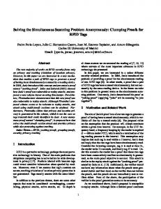
Fig. 1.
JAAVR Architecture.
B. JAAVR A challenge that we did not discuss so far is that no ATmega processor is openly available as synthesizable VHDL or Verilog code. We found several AVR-compatible processors at OpenCores [39], but none of them fulfilled our requirements of being fully synthesizable (as FPGA and ASIC), cycle-accurate, and well-tested. Therefore we (successfully) implemented our own version of an ATmega-compatible processor. Our processor is called Just Another AVR (JAAVR) and is based on an ATmega128 processor. In order to be maximally compatible with the ATmega128, we made sure that JAAVR has identical registers, an identical instruction-set, and an identical timing. We achieved this by using the documents [4], [5] and simulavr [46] as reference. In order to test the full instruction set, we wrote programs covering all available assembly instructions. First the compiled executable is run within a modified version of simulavr, which automatically generated test-vectors. A test vector contains the values of the processors register-file for each processing cycle. The identical program is then run on the VHDL model of JAAVR and in each cycle the content of the register-file is compared with the current test vector. JAAVR comes with three buses as it is shown in Figure 1: a synchronous program bus, a synchronous data bus, and an asynchronous I/O bus which is mapped within the data buses address range. The synchronous data and program buses ensure that it is possible to use area-efficient macros. Furthermore, JAAVR comes with 36 fixed-priority interrupts which can be cleared by the CPU. For an FPGA implementation we added a simple 604 bytes large UART bootloader. The program memory is synthesized as block RAMs which were initialized at runtime. With a fully functional VHDL design of an ATmegacompatible processor, it is possible to to apply several optimizations. Most notably are our performance optimizations which reduce the execution delay of several instructions. By operating a simple switch in our design, it is possible to
III. D ESIGN C ONCEPT Efficiently implementing cryptographic primitives for RFID tags and sensor networks is a challenging task. Most of the previously discussed papers concentrated on implementing a single cryptographic primitive. However, it is important to realize that those primitives are components of larger designs. In fact, the protocols to access those primitives have become so complex that it has become necessary to use tiny microprocessors instead of simple state machines. Such a microprocessor should be small, efficient (low-power, high performance-percycle), and easily programmable. In order to achieve those goals, it is not only necessary to build a small hardware design, but also to take care of a complete design-flow (e.g. simulator, assembler, compiler, debugger, ...). We decided to use the popular ATmega128 processor as the core of our architecture. This processor is one of the most popular 8-bit RISC processors ever designed and also well supported by available simulators [46], compilers (e.g. avr-gcc) and debuggers. Its 8-bit architecture, the dedicated I/O bus, and the flexible instruction-set make the processor perfectly suited to handle RFID and sensor-network protocols. A. ATmega128 Processor Developed in the 1990s, the AVR series by Atmel became one of the most popular 8-bit processors ever manufactured. A series of high-performance, low-power Atmel AVR processors evolved to the popular ATmega series. The ATmega series supports up to 133 instructions and comes with a wide range of peripherals. We decided to use the ATmega128 [4] as model. It is an 8-bit RISC processor with Harvard architecture, 32 general-purpose registers, an on-chip multiplier, 128 kbyte of Flash, 4 kbyte of EEPROM, and 4 kbyte of SRAM. It also supports boundary-scan JTAG as well as several timers, ADCs, UARTs, and an SPI and a TWI interface.
641 350
reduce the execution time of MUL, MULS, MULSU, FMUL, FMULS, FMULSU, ST, STD, PUSH, IJMP, RJMP, CBI, SBI (2 → 1), RCALL, ICALL, LPM, ELPM (3 → 2), and CALL, RET, RETI (4 → 3) instructions by one cycle. Experiments showed that these optimizations improved the performance of the subsequently discussed cryptographic functions by up to 30 %.
TABLE I C OMPARISON OF AES-128 IMPLEMENTATIONS . Version C version High-speed Low-RAM Eisenbarth et al. [12] Poettering et al. [42]
ROM [Bytes] 6,814 2,212 2,304 1,659 1,568
RAM [Bytes] 858 294 38 33 192
Runtime [Cycles] Enc. Dec. 6,502 7,938 3,290 4,534 3,490 4,630 4,557 7,015 3,629 4,462
IV. C RYPTOGRAPHIC P RIMITIVES Cryptographic services (confidentiality, data integrity, authentication, and non-repudiation) have to be defined depending on the application, environment, and necessary functionality. These goals can then be achieved by using standardized protocols, which are based on basic primitives, such as unkeyed, symmetric-key and public-key primitives. We decided to implement the popular AES standard, the SHA-3 finalist Grøstl, and the resource aware elliptic-curve-based public-key scheme. Our main goal concerning those three algorithms is to evaluate their runtime performance as well as their area footprint. As we will show in Section V, the chip-area consumption mainly depends on the size of the program memory (ROM) and the size of the necessary data memory (RAM). Security requirements such as side-channel awareness and countermeasures have not been evaluated explicitly, but were kept in mind during implementation. Because the ATmega128 and JAAVR have identical instruction-set timings, the following results are applicable for both processors. The average speedup of 30 % only applies when the compatibility mode is switched off.
the carry register, a reduction using the irreducible polynomial x8 ⊕ x4 ⊕ x3 ⊕ x ⊕ 1 is performed. This sequence of operations can be performed in constant time. In fact, all our AES implementations run in constant time and thus are safe from timing attacks. We implemented the MixColumns transformation using 48 XOR operations, 16 multiplications by 2, and 36 MOV instructions. 2) Results: Table I shows runtime, ROM, and RAM requirements of our and related AES implementations. A C version is given as reference in order to point out the margin exhausted by assembly implementations. In our high-speed design, an S-box lookup table was loaded to the RAM. By keeping the S-box within the program memory we were able to decrease the expensive RAM requirement from 294 to 38 bytes. In terms of runtime, even our RAM optimized implementation is still faster than Eisenbarth et al. [12] and Poettering et al. [42]. B. Grøstl When selecting a hash-function we decided not to go for the traditional ‘out-of-date’ hash function SHA-1, but focussed on one of the SHA-3 finalists. Based on the fact that Grøstl shares a lot of similarities with AES, it has been chosen for this work. Grøstl [18] is an iterated hash function operating on two distinct permutations P and Q and a compression function f . The input of the compression function is a message block m and a 512-bit chaining value h. For the construction of f the following definition is used f (h, m) = P (h ⊕ m) ⊕ Q(m) ⊕ h. The permutations P and Q are based on AES and thus consist of four transformations, known as AddRoundConstant, SubBytes, ShiftBytes, and MixBytes, which are applied several times. It comes to mind to actually combine the implementations of AES and Grøstl. In our highly optimized assembler implementations, AES and Grøstl share an S-box lookup table and temporary data memory. Apart from that, we had to keep the assembly implementations completely separated. 1) Implementations: In order to save processing cycles, the round transformations AddRoundConstant, SubBytes and ShiftBytes are handled consecutively. Hence, unnecessary RAM access can be avoided and a low memory footprint is ensured. The MixBytes transformation is the most expensive part in Grøstl as it involves a matrix multiplication within F256 . In order to reduce the needed amount of XOR and multiplicationby-2 operations, we followed the approach of Aoki et al [2]. Per column, MixBytes needs 48 XOR instructions, 9 MOV instructions and 16 multiply-by-2 operations.
A. AES AES [37] was standardized in 2001 and since then it has been used in a magnitude of applications and has become the most investigated symmetric-key cipher. AES is a round-based block cipher, operating on 128-bit data blocks, with an internal 128-bit state. The state is modified by iteratively applying the SubBytes, ShiftRows, MixColumns, and AddRoundKey transformations. Depending on the required security level, one can select from AES-128, AES-192 and AES-256, which vary on the size of the key and the number of applied round transformations. Having embedded applications in mind, we focus on AES-128. 1) Implementations: AES-128 uses a 128-bit key and performs the round transformations 10 times. The 128-bit state is constantly held in the registers R0-R15. In order to avoid loading the key twice, the key expansion step and the AddRoundKey transformation have been merged into a single function. Thus also expensive RCALL and RET instructions can be evaded. Due to the fact that MixColumns applies a transformation on every column of the state matrix, this is the most expensive part of AES. For an efficient implementation of MixColumns, the needed amount of XOR and multiplication operations has been reduced to a minimum. A multiplication with 2 is performed by consecutively executing an ADD, BRCC and EOR operation. ADD is used to do a right shift and depending on
642 351
TABLE II C OMPARISON OF G RØSTL -256 IMPLEMENTATIONS . Version High-speed Balanced Low RAM Ipsen [29] Roland [45] Roland [45]
ROM [Bytes] 4,990 1,406 1,792 4,684 4,228 4,170
RAM [Bytes] 534 536 216 602 994 226
Runtime [Cycles] 55 bytes 2776 bytes 41,232 1,230,722 44,830 1,337,477 50,006 1,490,917 87,643 2,636,561 50,105 1,301,944 49,610 1,471,280
2) Results: In the following (see Table II), three highlyoptimized assembly implementations of Grøstl-256 are presented. They focus on efficient usage of memory and computation resources and thereby yield results, which outperform existing solutions. A speed-optimized version makes extensive use of assembly macros and omits expensive RCALL (3 cycles) and RET (4 cycles) instructions. Due to the elimination of unused overhead, the high-speed version needs only 443 cycles/byte for a message with 2776 bytes. A disadvantage of this technique is that the code size increases to 4,990 bytes as the MixBytes routine is embedded 16 times. The balanced version is very similar to the high-speed version but does not embed MixBytes using assembly macros. Like MixBytes, the SubBytes step is applied on all columns and therefore can be integrated within MixBytes in order to evade redundant code. As a consequence, the code size minimizes to 1,406 bytes. The low-RAM version is especially suited for devices with small RAM, because the S-box values are loaded from program memory. Therefore the RAM access instruction LD (2 cycles) is replaced by the instruction LPM (3 cycles) which accesses the program memory. As a result of this, the cycles per byte raise up to 537 bytes for a long message but the consumed RAM reduces to 216 bytes. Table II also shows performance results of our and related implementations. The program memory values include 256 bytes for the S-box. Compared to related work [2], [29], [45], our implementations outperform them in terms of speed and memory.
Cycles / Byte 55 bytes 2776 bytes 750 443 815 482 909 537 1,594 950 911 469 902 530
1) Implementations: The most important design decision when implementing elliptic curves is which elliptic curve and which underlying finite field to use. We decided to use prime fields because the ATmega128 comes with an integrated 8bit multiplier. Further we decided to use the popular curves secp160-256r1 standardized within the SECG [9], [10] and NIST [38] standards. The secp160r1 elliptic curve has been removed from the latest version of the standards but we use it as reference as most related work focused on this elliptic curve. The most expensive block within hardware and embeddedsystem design is data memory. Therefore, the most expensive algorithms are public-key algorithms. Therefore it was especially important to carefully choose how to implement elliptic curve cryptography on JAAVR, respectively on an ATmega128. We selected to use the latest Montgomery-ladder formulas by Hutter et al. [25]. They require only seven registers, 16 field multiplications, and 17 addition operations, while guaranteeing a constant number of field operations as well as some basic resistance against side-channel attacks. On the level of prime-field operations we used a binary inversion algorithm based on the Extended Euclidian algorithm as well as highly assembly-optimized multiplication, addition and subtraction methods. We took advantage of the special Mersenne-like primes and performed reductions by only using addition, subtraction, and shift operations. 2) Results: In our experiments we varied both the elliptic curve and the used multi-precision multiplication formulas. As shown in Table III, we investigated the impact of operandscanning (OS), product-scanning (PS), and the newly introduced operand-caching (OC) [26] multiplication methods on runtime and program memory (ROM) size. As reference we also provide results using operand-scanning, written in C compiled with avr-gcc V4.5 with the ‘-Os’ flag enabled. While ‘-O1’ gave similar (but larger) results, ‘-O2’ and ‘-O3’ deteriorated both the runtime and code size. While using the fast operand-caching method, runtime improvements of factors between 2.7 and 3.4 where possible, compared to the pure C version, but the size of the program memory also increased by factors between 2.0 and 3.1. However, using a looped instead of an unrolled operand-caching implementation decreased the size of the program memory by 29-52 %. In comparison to related work by Gura et al. [19] and Szczechowiak et al. [47], our runtime performance is inferior
C. Elliptic Curve Cryptography Nowadays there exist three well-established public-key schemes (RSA [44], ElGamal [13], and ECC [31]) which are complementarily used in many applications. From those three, elliptic curve schemes need fewer data memory and outperform RSA and ElGamal on many embedded architectures (cf. [19]). The security of elliptic curves is based on the Elliptic Curve Discrete Logarithm Problem. Up to now, only generic attacks on elliptic curves have been found (Baby-step giantstep, Pollard-Rho) and therefore it is possible to compute ECC (compared to RSA and ElGamal) on relatively small finite fields. For further details on elliptic curve cryptography, we refer the interested reader to the following books [11], [21].
643 352
TABLE IV RFID HARDWARE DESIGNS .
TABLE III E LLIPTIC C URVE PERFORMANCE EVALUATION . Curve
Implementation
secp160r1
pure C, OS PS looped OC looped OC unrolled pure C, OS OC looped OC unrolled pure C, OS OC looped OC unrolled pure C, OS OC looped OC unrolled Gura et al. [19] Gura et al. [19] Gura et al. [19] Szczechowiak et al. [47]
secp192r1 secp224r1 secp256r1 secp160r1 secp192r1 secp224r1 160-bit curve
ROM [Bytes] 3,864 4,180 5,546 7,762 3,706 5,720 9,290 3,706 5,570 11,372 5,114 7,132 14,924 3,682 3,979 4,812 46,100
Hardware design
Runtime [kCycles] 35,101 20,440 13,787 13,027 52,265 16,573 15,371 81,172 29,688 27,633 122,960 46,117 43,057 6,480 9,920 17,520 9,376
(1) Flexible (2) ISO14443A using timer (3) ISO14443A using HW modem
Area w/o Macros w/ Macros [GE] [GE] 295,782 82,530 8,962 8,222 -
Power [uW] 77,6 57.0
12 kGE. So JAAVR is 19 % and 46 % smaller compared to those other processor designs. The area of 6459 GE is shared between various function blocks: 1,664 GE are general purpose registers, 786 GE are the multiplexers used to access those registers, 799 GE belong to the ALU, 468 GE are needed for the multiplier, 661 GE is the size of the instruction decoder, and 183 GE are spent on the interrupt controller. The remaining chip area is needed by other internal registers (SREG, SP, PC) and address generation. Due to the fact that in RFID chip-area is most significant, we also designed a slimmed-down version of JAAVR. In JAAVRslim we removed the multiplier (which is actually only used within ECC) and slightly changed the MOVW instruction. It now needs 2 cycles to complete. Thus a fairly large internal multiplexer could be avoided. JAAVR-slim requires 5,053 GE which is about 22 % smaller than JAAVR. When JAAVR is synthesized on the Xilinx Spartan-3 FPGA, it requires 1,078 slices and has a maximum frequency of 28 MHz.
to theirs. This is easily explained by investigating the used point-multiplication formulas. While Gura et al. used an NAFmethod for point multiplication (which is not side-channel secure), Szczechowiak et al. used a Comb method with 16 pre-computed points, resulting in a large program memory. Summarizing our software results, we can say that even 160-bit ECC is 317 times slower than Grøstl and 3,960 times slower than AES, rendering AES and Grøstl superior for any real-time applications. In terms of program memory, ECC is only 1.67 and 2.64 times larger compared to AES and Grøstl. It is important to note that 160-bit ECC only offers a security level of 80-bit, while both AES-128 and Grøstl-256 offer a security level of 128-bit. By applying 256-bit ECC with a security level of 128-bit the runtime would increase by a factor of 3.5.
B. JAAVR performing ISO14443-A Using JAAVR, many applications can be investigated. Common applications such as sensor networks or RFID tags are components of the upcoming Internet of Things (IoT). From a system designer’s perspective it is necessary to achieve small, low-power/energy designs that are capable of communicating with a certain protocol. In this work we decided to take a deeper look at RFID. Passive RFID tags are supplied via an electromagnetic field. The amount of energy that arrives at the actual microchip is dependent on the distance between the RFID reader and the tag. The larger the operating distance, the less energy is available for the RFID tag. Or in other words, the more energy consumed by the RFID tag, the shorter is the possible operating distance. In the case of near-field-communication (NFC), several Milliwatts of power are realistic. In the following we present three solutions, all capable of performing various RFID protocols (cf. Table IV). All these designs have been practically evaluated using the HF FPGA DemoTag presented by Plos et al. [40]. This prototyping platform comes with a discretely built analog front-end and the previously mentioned Spartan-3 FPGA. This DemoTag is also available in a different version which is equipped with an ATmega processor instead of an FPGA. This tag comes with a development platform and is shipped with a firmware, capable of communicating with ISO 14443 [27], ISO 15693 [28], and NFC. In fact, for our
V. H ARDWARE R ESULTS In the following we discuss several results, which we accumulated during our experiments. First, we take a look at the JAAVR processor. Second, we use JAAVR to perform over-the-air communication using an RFID protocol and third, we compare the different impacts of the previously described primitives on our lowest-cost RFID solution. For the following results we used the UMC 130 nm lowleakage CMOS process technology with Faraday design libraries. Further, we used Cadence RTL Compiler v08.10 to synthesize, Cadence First Encounter v08.10 to place and route, NCSim v08.20 to simulate and Cadence First Encounter v08.10 for power simulation. As FPGA platform we used a Spartan-3 XC3S1000-5FTG256C in connection with Xilinx ISE Design Suite v13.3. A. JAAVR A complete fully-compatible version of the JAAVR processor needs 6,459 GE. In comparison, the popular 16-bit OpenMSP430 [39] processor requires 8 kGE. ARM’s newly designed 32-bit Cortex-M0 processor [3] requires around
644 353
TABLE V JAAVR- SLIM WITH ISO-14443-A DIGITAL HARDWARE FRONT- END .
first design approach we simply modified this ready-to-use firmware which resulted in a very flexible RFID solution. Synthesis showed that 295,782 GE would be required to actually manufacture it. The flexible design comes with an 29,454 bytes large program memory, a 4 kByte SRAM (same size as the original ATmega128), two 8-bit timers, two 16-bit timers, one UART, and 44 general-purpose I/O pins (GPIO). Timer, UART and GPIOs are fully compatible with the original ATmega128. The by far largest components of this flexible RFID architecture are the program and data memories. Thus, in the following we distinguish between two design principles which are probably not applicable for every design process: the question is whether RAM, ROM, Flash, or EEPROM macros can be used in one’s design process. For the used UMC 130 nm low-leakage technology, we have access to both RAM and ROM macros. Building the same flexible design using macros would decrease its chip area to 82,530 GE. However, this is still too expensive for cost-critical RFID applications. For the practical FPGA evaluation, the data and program memories were synthesized using block RAMs and a bootloader was added to initialize the program memories. After setting a simple jumper, it is possible to update the firmware running on JAAVR via UART. This FPGA implementation has been used to practically verify that the hardware design is capable of doing wireless RFID communication with a standard reader. In our second solution (cf. Table IV) we decided to get rid of all unnecessary components and concentrate on a single RFID protocol: ISO 14443A. This is the same underlying protocol which is currently supported by the latest Google phones. The design only consists of a single timer, some GPIOs, as well as specially fitted program and data memories. In order to achieve a chip area of 8,962,GE, we used JAAVR-slim instead of JAAVR. For the first two hardware solutions we simply used and synthesized the Atmel compatible Timer, and GPIO components. Now that we have a fully synthesizable and flexible design framework (JAAVR) at our disposal, we are able to add custom components. For our third solution (cf. Table IV), we added a dedicated ISO 14443A digital hardware modulation and demodulation front-end (modem). As a result, all timers and GPIOs could be removed and outstanding chip-area and power results were achieved. Additionally it is possible to reduce the clock frequency of JAAVR from 13.56 MHz (the carrier frequency) down to an integer fraction of it to further reduce the power consumption. Table V lists the detailed chip area and power requirements for this highly optimized hardware solution consisting of: JAAVR-slim, a 606 bytes large ROM, an 8-byte RAM, and an ISO 14443A hardware modem. The modem stores incoming data in an IO-mapped, triple buffered, 8-bit register and automatically performs CRC checks. Command handling is all done by JAAVR-slim using plain C-software. A possible assembly implementation could avoid any RAM usage at all and would potentially minimize power consumption and ROM size as well. In order to reduce the necessary CPU frequency
Module JAAVR-slim ROM RAM Modem Misc Total
Area [um2 ] [GE] 25,871 5053 7,194 1,405 2,565 501 5,974 1,167 491 96 42,095 8,222
1.13 MHz 12.4 2.9 0.4 10.0 31.3 57.0
Power [uW] 3.39 MHz 13.56 MHz 34.0 149.2 8.9 36.9 1.0 4.3 10.4 13.0 37.1 37.1 91.4 240.5
and data-memory requirements as much as possible, each data byte is processed immediately after it has been received. This approach leads to a minimal CPU frequency of 1.13 MHz. The change of the clock pre-scaler has a direct impact in the power consumption of JAAVR-slim. However, the modem is always clocked with 13.56 MHz. The resulting power values between 57 μW and 240.5 μW make our design well suited for RFID and ready to add cryptography. C. JAAVR with Cryptographic Primitives in Software Up until now, much research has been performed on dedicated cryptographic hardware designs. In this subsection we show a very flexible design approach in which the program memory and appropriate data memories are synthesized and the impact of AES, Grøstl, and ECC on our total chip area as well as our power consumption is measured. Table VI lists the detailed results of several experiments. The most important factors concerning chip size are the program memory, the data memory, and whether JAAVR or JAAVR-slim has been used. JAAVR-slim was used for AES and Grøstl, and JAAVR was used for ECC. As it turns out, the ROM macros available to us, are much larger than the synthesized program memories. This is why we only considered synthesized program memories. Further, the size of the data memory has a significant influence on the total areaconsumption. For all algorithms we used the data-memory sizes evaluated in the preceding software implementations. In the following we do not only consider the total area consumption of our software-only solutions but also discuss the the difference in hardware requirements for doing cryptography. 1) AES: Our most significant result concerning AES is that in our case using a dedicated AES hardware extension is more efficient than our software-only solution. The AES core by Feldhofer et al. [16] requires 3,400 GE, while 5,367 GE need to be added in our software-only solution using JAAVR. Compared to the stand-alone JAAVR tag without cryptography, the power consumption increased by a factor between 1.3 and 2.5 but is still within reasonable boundaries. 2) Grøstl: The biggest difference between Grøstl and AES is the size of the necessary internal state matrix. We are capable of taking advantage of RAM macros, so the area increase compared to AES is quite negligible. Neither Tillich et al. [48], nor Henzen et al. [23] use RAM macros, so their hardware designs (14.6 kGE and 25 kGE) are larger than our softwareonly solution (14 kGE) with RFID interface.
645 354
TABLE VI I MPACT OF CRYPTOGRAPHIC PRIMITIVES ON CHIP AREA AND POWER . Crypto Algorithm w/o crypto AES Grøstl Grøstl & AES ECC AES & Grøstl & ECC
ROM Size Area [Byte] [GE] 604 1,405 3,590 5,833 2,822 4,927 5,382 7,534 4,968 7,790 9,234 13,330
Size [Byte] 8 38 216 216 384 384
RAM synth. w/ Macro [GE] [GE] 501 2,322 1,376 12,707 2,671 12,704 2,671 22,458 3,653 22,463 3,653
TABLE VII C OMPARISON WITH RELATED WORK . Crypto Algorithm AES Grøstl ECC AES [16] Grøstl [48] Grøstl [23] ECC Fp192 [49] ECC F2163 [34]
Crypto Area [GE] +5,367 +5,798 +9,684
Total Area [GE] 13,589 14,020 17,906 3,400 14,622 25,000 23,818 12,506
Crypto w/ Macro [GE] +5,367 +5,798 +8,391 +9,684 +15,271
Total w/ Macro [GE] 8,222 13,589 14,020 16,613 17,906 23,493
1.13 MHz [uW] 57.0 75.0 69.0 75.0 -
Power 3.39 MHz [uW] 91.4 131.9 117.6 131.9 -
13.56 MHz [uW] 240.5 351.4 332.2 351.4 484.8 484.8
With an improved instruction-set timing it is even possible that JAAVR outperforms its model ATmega128 processor doing cryptography by up to 30 %. However, we have not yet tapped the real potential of our design. Future work is going to both improve the runtime performance and chip-area of our cryptographic implementations by using instruction-set extensions and merging cryptographic hardware components with the JAAVR core.
Power [uW/MHz] 25.91 24.50 35.75 45.00 2,210.00 500.00 32.42
ACKNOWLEDGMENT The work described in this paper has been supported in part by the European Commission through the ICT programme under contract ICT-2007-216676 ECRYPT II.
3) ECC: Compared with AES and Grøstl, ECC needs an about two times larger program memory and is several magnitudes slower. So running it with a frequency of less than 13.56 MHz would result in an execution time of several seconds which is unpractical for real-time applications. For the ECC results we used the assembler optimized secp160r1 implementation using a looped product-scanning multiplication method. A memory with only 384 bytes is necessary. The area results of 17,9 kGE and the difference of 9.6 kGE are quite promising compared to the prime-field area results of Wolkerstorfer et al. [49]. 4) AES & Grøstl & ECC: When AES & Grøstl or AES & Grøstl & ECC are linked together and synthesized simultaneously, the real advantage of our software-only based design methodology can be observed. The total area consumption of 23.5 kGE combines AES, Grøstl, and ECC, as well as an ISO14443-A wireless RFID interface and is much smaller than the sum of the smallest implementations in the related work. In relation to that, Hutter et al. [24] need 21.5 kGE to combine AES and ECDSA. However, an RFID interface was not part of their design.
R EFERENCES [1] A. Abrial, J. Bouvier, M. Renaudin, P. Senn, and P. Vivet. A new contactless smart card IC using an on-chip antenna and an asynchronous microcontroller. Solid-State Circuits, IEEE Journal of, 36(7):1101–1107, July 2001. [2] K. Aoki, G. Roland, Y. Sasaki, and M. Schl¨affer. Byte slicing grøstl - optimized intel aes-ni and 8-bit implementations of the sha-3 finalist grøstl. 2011. in press. [3] ARM. ARM Homepage. Available online at http://www.arm.com/ products/processors/cortex-m/cortex-m0.php. [4] Atmel Corporation. 8-bit AVR Microcontroller with 128K Bytes InSystem Programmable Flash. Available online at http://www.atmel.com/ dyn/resources/prod documents/doc2467.pdf, August 2007. [5] Atmel Corporation. 8-bit AVR Instruction Set. Available online at http://www.atmel.com/dyn/resources/prod documents/doc0856. pdf, May 2008. [6] A. Auer. Scaling Hardware for Electronic Signatures to a Minimum. Master thesis, University of Technology Graz, October 2008. [7] L. Batina, N. Mentens, K. Sakiyama, B. Preneel, and I. Verbauwhede. Low-Cost Elliptic Curve Cryptography for Wireless Sensor Networks. In L. Butty´an, V. Gligor, and D. Westhoff, editors, Security and Privacy in Ad-Hoc and Sensor Networks – ESAS, volume 4357, pages 6–17, Berlin Heidelberg, 2006. Springer-Verlag. [8] H. Bock, M. Braun, M. Dichtl, E. Hess, J. Heyszl, W. Kargl, H. Koroschetz, B. Meyer, and H. Seuschek. A Milestone Towards RFID Products Offering Asymmetric Authentication Based on Elliptic Curve Cryptography. Invited talk at RFIDsec 2008, July 2008. [9] Certicom Research. Standards for Efficient Cryptography, SEC 2: Recommended Elliptic Curve Domain Parameters, Version 1.0. Available online at http://www.secg.org/, September 2000. [10] Certicom Research. Standards for Efficient Cryptography, SEC 2: Recommended Elliptic Curve Domain Parameters, Version 2.0. Available online at http://www.secg.org/, January 2010. [11] H. Cohen, G. Frey, R. Avanzi, C. Doche, T. Lange, K. Nguyen, and F. Vercauteren, editors. Handbook of elliptic and hyperelliptic curve cryptography. Discrete Mathematics and its Applications (Boca Raton). Chapman & Hall/CRC, Boca Raton, FL, 2006. [12] T. Eisenbarth, T. Gneysu, S. Heyse, S. Indesteege, S. Kerckhof, F. Koeune, T. Nad, T. Plos, F. Reggazoni, F.-X. Standaert, and L. van Oldeneel tot Oldenzeel5. Compact Implementation and Performance Evaluation of Block Ciphers in ATtiny Devices. In ECRYPT Workshop on Lightweight Cryptography, Belgium, November 2011.
VI. C ONCLUSION In this paper we presented a flexible design approach, using a standard microprocessor to combine RFID and cryptographic functionalities. We improved current AES and Grøstl implementations in terms of speed and memory footprint on the ATmega128 and also evaluated state-of-the-art ECC pointmultiplication methods, varying the security margin and the used multi-precision multiplication methods. Our hardware results are manifold. We both presented a programmable, digital RFID solution, just needing 8,222 GE, as well as an RFID design capable of performing AES, Grøstl, and ECC (three basic cryptographic primitives) requiring only 23.5 kGE.
646 355
[31] N. Koblitz. Elliptic Curve Cryptosystems. Mathematics of Computation, 48:203–209, 1987. [32] S. S. Kumar and C. Paar. Are standards compliant Elliptic Curve Cryptosystems feasible on RFID? In Workshop on RFID Security 2006 (RFIDSec06), July 12-14, Graz, Austria, 2006. [33] J.-W. Lee, D. H. T. Vo, Q.-H. Huynh, and S. H. Hong. A Fully Integrated HF-Band Passive RFID Tag IC Using 0.18-μm CMOS Technology for Low-Cost Security Applications. volume 58, pages 2531–2540, June 2011. [34] Y. K. Lee, K. Sakiyama, L. Batina, and I. Verbauwhede. Elliptic-CurveBased Security Processor for RFID. IEEE Transactions on Computers, 57(11):1514–1527, November 2008. [35] S. Masui, E. Ishii, T. Iwawaki, Y. Sugawara, and K. Sawada. A 13.56 MHz CMOS RF identification transponder integrated circuit with a dedicated CPU. In Solid-State Circuits Conference, 1999. Digest of Technical Papers. ISSCC. 1999 IEEE International, pages 162–163, February 1999. [36] A. Moradi, A. Poschmann, S. Ling, C. Paar, and H. Wang. Pushing the Limits: A Very Compact and a Threshold Implementation of AES. In K. G. Paterson, editor, Advances in Cryptology - EUROCRYPT 2011. Proceedings, volume 6632 of Lecture Notes in Computer Science, pages 69–88. Springer, 2011. [37] National Institute of Standards and Technology (NIST). FIPS-197: Advanced Encryption Standard, November 2001. Available online at http://www.itl.nist.gov/fipspubs/. [38] National Institute of Standards and Technology (NIST). FIPS-186-3: Digital Signature Standard (DSS), 2009. Available online at http://www. itl.nist.gov/fipspubs/. [39] OpenCores. OpenCores Homepage. Available online at http://opencores. org/, November 2011. [40] T. Plos, M. J. Aigner, T. Baier, M. Feldhofer, M. Hutter, T. Korak, and E. Wenger. Semi-Passive RFID Development Platform for Implementing and Attacking Security Tags. International Journal of RFID Security and Cryptography, 1:16–24, 2012. [41] T. Plos and M. Feldhofer. Hardware Implementation of a Flexible Tag Platform for Passive RFID Devices. In Proceedings of the 14th Euromicro Conference on Digital System Design Architectures, Methods and Tools (DSD 2011). Proceedings, pages 293–300. IEEE Computer Society, August 2011. ISBN 978-1-4577-1048-3. [42] B. Poettering. AVRAES: The AES block cipher on AVR controllers, March 2007. Available online at http://point-at-infinity.org/avraes/. [43] P. Rakers, L. Connell, T. Collins, and D. Russell. Secure Contactless Smartcard ASIC with DPA Protection. IEEE Journal of Solid-State Circuits, 36(3):559–565, March 2001. ISSN 0018-9200. [44] R. L. Rivest, A. Shamir, and L. Adleman. A Method for Obtaining Digital Signatures and Public-Key Cryptosystems. Communications of the ACM, 21(2):120–126, February 1978. ISSN 0001-0782. [45] G. Roland. Efficient Implementation of the Grøstl-256 Hash Function on an ATmega163 Microcontroller. Master’s thesis, Institute for Applied Information Processing and Communications (IAIK), Graz University of Technology, Inffeldgasse 16a, 8010 Graz, Austria, June 2009. [46] K. Rudolph, J. Wunsch, E. Weddington, and J. Sherrill. Simulavr: an AVR simulator, November 2011. Available online at http://http://www. nongnu.org/simulavr/. [47] P. Szczechowiak, L. B. Oliveira, M. Scott, M. Collier, and R. Dahab. NanoECC: Testing the Limits of Elliptic Curve Cryptography in Sensor Networks. In R. Verdone, editor, Wireless Sensor Networks 5th European Conference, EWSN 2008, Bologna, Italy, January 30-February 1, 2008. Proceedings., volume 4913 of Lecture Notes in Computer Science, pages 305–320. Springer, 2008. [48] S. Tillich, M. Feldhofer, W. Issovits, T. Kern, H. Kureck, M. M¨uhlberghuber, G. Neubauer, A. Reiter, A. K¨ofler, and M. Mayrhofer. Compact Hardware Implementations of the SHA-3 Candidates ARIRANG, BLAKE, Grøstl, and Skein. Cryptology ePrint Archive, Report 2009/349, 2009. [49] J. Wolkerstorfer. Is Elliptic-Curve Cryptography Suitable for Small Devices? In Workshop on RFID and Lightweight Crypto, July 13-15, 2005, Graz, Austria, pages 78–91, 2005.
[13] T. ElGamal. A Public Key Cryptosystem and a Signature Scheme Based on Discrete Logarithms. In Advances in Cryptology - CRYPTO ’84, Santa Barbara, California, USA, August 19-22, 1984, Proceedings, volume 196 of LNCS, pages 10–18. Springer, 1984. [14] M. Feldhofer, S. Dominikus, and J. Wolkerstorfer. Strong Authentication for RFID Systems Using the AES Algorithm. In CHES, pages 357–370, 2004. [15] M. Feldhofer and J. Wolkerstorfer. Strong Crypto for RFID Tags - Comparison of Low-Power Hardware Implementations. In IEEE International Symposium on Circuits and Systems (ISCAS 2007), New Orleans, USA, May 27-30, 2007, Proceedings, pages 1839–1842. IEEE, May 2007. [16] M. Feldhofer, J. Wolkerstorfer, and V. Rijmen. AES Implementation on a Grain of Sand. IEEE Proceedings on Information Security, 152(1):13– 20, October 2005. [17] F. F¨urbass and J. Wolkerstorfer. ECC Processor with Low Die Size for RFID Applications. In Proceedings of 2007 IEEE International Symposium on Circuits and Systems. IEEE, IEEE, May 2007. [18] P. Gauravaram, L. R. Knudsen, K. Matusiewicz, F. Mendel, C. Rechberger, and S. S. T. Martin Schl¨affer. Grøstl – a SHA-3 candidate. Document version 2.0, available online at http://www.groestl.info/Groestl.pdf, March 2011. [19] N. Gura, A. Patel, A. Wander, H. Eberle, and S. C. Shantz. Comparing Elliptic Curve Cryptography and RSA on 8-Bit CPUs. In M. Joye and J.J. Quisquater, editors, Cryptographic Hardware and Embedded Systems – CHES 2004, Proceedings, volume 3156 of Lecture Notes in Computer Science, pages 119–132. Springer, 2004. [20] P. H¨am¨al¨ainen, T. Alho, M. H¨annik¨ainen, and T. D. H¨am¨al¨ainen. Design and Implementation of Low-Area and Low-Power AES Encryption Hardware Core. In 9th EUROMICRO Conference on Digital System Design: Architectures, Methods and Tools (DSD 2006). Proceedings, pages 577–583. IEEE Computer Society, September 2006. [21] D. Hankerson, A. J. Menezes, and S. Vanstone. Guide to Elliptic Curve Cryptography. Springer, Berlin, Germany / Heidelberg, Germany / London, UK / etc., 2004. [22] D. Hein, J. Wolkerstorfer, and N. Felber. ECC is Ready for RFID - A Proof in Silicon. In Selected Areas in Cryptography, 15th International Workshop, SAC 2008, Sackville, Canada, August 14-15, 2008, Revised Selected Papers, Lecture Notes in Computer Science (LNCS), September 2008. [23] L. Henzen, P. Gendotti, P. Guillet, E. Pargaetzi, M. Zoller, and F. K. G¨urkaynak. Developing a Hardware Evaluation Method for SHA-3 Candidates. In Cryptographic Hardware and Embedded Systems – CHES 2010. Proceedings, volume 6225 of Lecture Note in Computer Science, pages 248–263, Santa Barbara, CA, 2010. Springer-Verlag. [24] M. Hutter, M. Feldhofer, and J. Wolkerstorfer. A Cryptographic Processor for Low-Resource Devices: Canning ECDSA and AES like Sardines. In C. A. Ardagna and J. Zhou, editors, Information Security Theory and Practices. Proceedings, volume 6633 of Lecture Notes in Computer Science, pages 144–159. Springer, 2011. [25] M. Hutter, M. Joye, and Y. Sierra. Memory-Constrained Implementations of Elliptic Curve Cryptography in Co-Z Coordinate Representation. In A. Nitaj and D. Pointcheval, editors, Progress in Cryptology AFRICACRYPT 2011. Proceedings, volume 6737 of Lecture Notes in Computer Science, pages 170–187. Springer, 2011. [26] M. Hutter and E. Wenger. Fast Multi-Precision Multiplication for Public-Key Cryptography on Embedded Microprocessors. In B. P. und Tsuyoshi Takagi, editor, Cryptographic Hardware and Embedded Systems – CHES 2011. Proceedings, volume 6917 of Lecture Notes in Computer Science, pages 459–474. Springer, 2011. [27] International Organization for Standardization (ISO). ISO/IEC 14443-3: Identification Cards - Contactless Integrated Circuit(s) Cards - Proximity Cards - Part3: Initialization and Anticollision. Available online at http: //www.iso.org, 2001. [28] International Organization for Standardization (ISO). ISO/IEC 18000-3: Information Technology AIDC Techniques — RFID for Item Management – Part 3: Parameters for air interface communications at 13.56 MHz, March 2004. [29] M. S. Ipsen. C-Implementation of Grøstl Optimized for 8-bit Architectures, December 2011. submitted to ebash. [30] J.-P. Kaps. Cryptography for Ultra-Low Power Devices. PhD thesis, ECE Department, Worcester Polytechnic Institute, Worcester, Massachusetts, USA, May 2006.
647 356