assembly equipment (dicing, adhesive die attach, and wire bonding equipment). ... chips ("Known-Good Die") and lack of package .... low Young's modulus, etc.
Laminated Memory: A New 3-Dimensional Packaging Technology for MCMs D. B. Tuckerman, L.-0. Bauer, N. E. Brathwaite, J. De&, K. Flatow, R. Hsu, P. Kim,C.-M. Lin, K.Lin, S. Nguyen, V. Thipphavong nCHIP, Inc., 1971 N.Capitol Avenue, San Jose, CA 95132 USA
Abstract
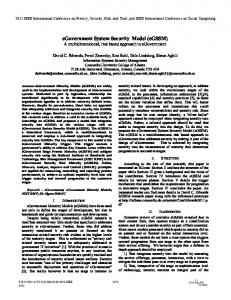
advantage of the very high interconnection density which an MCM-D substrate can provide: for example, an application containing a large number of relatively lowpinout memory chips, as illustrated in Figure l(a).
A new, low-cost, manufacturable process for stacking memory chips up to four-high on a multichip module (MCM)substrate is described. Theprocess is particularly useful when utilized with a high-performance thin-film interconnection substrate ("MCM-D"), as the technique typically enables large ( 2 - 4 ~reductions ) in substrate cost for memory-intensive designs, with only a small increment in assembly cost, thereby achieving lower total MCM cost, and greater utilization of the high wiring density and good thermal conductivity of the MCM substrate. The technology was developed and demonstrated using commercially available MCM assembly equipment (dicing, adhesive die attach, and wire bonding equipment). Fully functional memory modules incorporating 2-high stacks have beenfdricated, and have passed basic thermal shock rests.
I I
(a) Conventional assembly
(-2x area reduction)
Figure 1: Typical MCM layouts In such an application, the use of an MCM substrate technology having lower cost per unit area ($/cm2) would be appropriate (e.g., organic laminate "MCM-L" or cofired ceramic "MCM-C"), provided that the wiring density, electrical perfarmance, and t h e m performance all remain acceptable. The example of Figure l(a) is in fact a relatively common type of MCM application. Modern microprocessor systems are often designed so that all the logic functions are incorporated into a few (often only one) high pinout chips (e.g., central processing unit, floating point unit, and memory management unit). To achieve maximum performance, a significant number of cache memory chips (sometimes as many as 20) are also required, and the cache access operation may be a critical path for the system. In such cases, system performance is maximized by including the cache chips on a multichip module with the logic chips, thereby minimizing propagation delays. It would be very desirable to be able to economically package such a module using MCM-D technology, to take advantageof the superior electrical and thermal performance which MCM-D can provide [3].
1: Introduction Multichip modules (MCMs) provide a means for interconnecting integrated circuits (ICs) so as to achieve higher system performance, much smaller physical size and weight, reduced power consumption, and increased reliability, compared with the conventional method of interconnecting singlechip packages on a printed circuit board (PCB). However, the cost of manufacturing an MCM is often higher than its conventionally packaged equivalent. To some extent this higher cost has been due to inadequacies in the technological infrastructure,such as unavailability of fully tested and burned-in unpackaged IC chips ("Known-Good Die") and lack of package standardization; it is now clear that these inadequacies are gradually being overcome [1,2]. However, the cost of manufacturing MCM interconnection substrates, particularly when using thin-film technology (often called "MCM-D" technology), is still too high to be competitive in certain cost-sensitive applications. This is most apparent in applications which do not take full
0-8186-5560-7194 $03.00 0 1994 IEEE
(b) Laminated Memory
58
and Thomson-CSF 181 have developed related 3dimensional technologies which differ in the technological details. Yet other methods have been patented by Unisys [9] and Matsushita [lo]. In general, these methods require customization of the memory chip padout (i.e., placement of all bond pads along one edge) and may involve complex processing along the stack edge, for example, laser processing. TAB bonding, or other relatively high-cost steps. With two exceptions [6, 101, the memory stacks are generally designed to be mounted vertically, i.e., in an orientation such that the IC chips are perpendicular to the MCM substrate, which implies that the overall package must be. quite thick, e.g., 10 mm or so. In most practical MCM applications, however, overall package thickness is a critical parameter which the designer wishes to minimize to 3 4 mm, or even less, due to tight spacing between adjacent PC boards and/or the need for adequate vertical space for air flow and heat sinking. The methods of Refs. [6] and [ 103 involve "flat" stacking of the chips (i.e., parallel to the plane of the MCM substrate) and so can have lower p f d e . However, both methods still occupy substantial vertical space either because of the need for an extra redistribution chip [6] or because of the use of additional spacer layers between the chips (0.6 mm chip pitch in Ref. [lo]). In view of the above background, nCHIP, Inc. perceived a need for a memory stacking technology which is low cost, uses off-the-shelf memory chips, does not use exotic or expensive processing, and enables the chips to be stacked "flat" with very close spacing (4.4 mm chip pitch), so that short ( 2 4 chip) stacks could be produced without increasing overall package thickness. (It is not necessary that the technology be extendable beyond 4-high stacks, as the benefits of still higher stacks are negligible in terms of reduced module a m , and would be outweighed by the complications caused by increased package thickness.) Such a technology, "Laminated Memory", has been developed by nCHIP for use on its MCM-D substrate technology [3] and will be described in this pager.
This paper describes a new, low-cost method for interconnecting ICs on an MCM. The method enables a large reduction in the surface area of the MCM by stacking small groups of 2-4 identical chips in the vertical dimension 141, as illustrated in Figure 1@). We will refer to this new technology as "Laminated Memory". The substrate area reduction for actual MCM design case studies is typically in the range of 1.5x-3x, which typically leads to a 24x reduction in the manufacturing cost of the MCM subshate. m e super-linear relationship between cost and area is a result of two factors: first, because the number of substrates which can be manufactured on a single wafer or panel is a relatively small integer, and so a seemingly small reduction in area can alter the layout from, say, a one-per-wafer to a twoper-wafer design; second, because smaller substrates normally yield beuer than larger substrates. even when the overall wiring complexity is unchanged.) The resultant increase in routing density leads to much more efficient use of the highdensity interconnection capability of an MCM-D SubSW. Unlike most alternative schemes for 3dimensional memory packaging, Laminated Memory technology is derived from conventional dicing, die attach and wire bonding processes, thereby leveraging the existing technology infrastructure for IC and MCM assembly. It therefore greatly expands the range of applications for which MCM-D is the packaging technology of choice. While the Laminated Memory technology may, in some cases, also be applied to MCM-L and MCM-C technologies to effect area reductions, in most cases it would be difficult for those alternatives to accommodate the increased heat flux and denser wiring without the introduction of additional interconnect layers which would result in a net increase in substrate cost, rather than a decrease as occurs with MCM-D substrates. Thus, the Laminated Memory technology can be a major cost reducer for MCM-D technology compared to its altematiVeS. The cost of Laminated Memory assembly has been calculated to be about 35% grater than for conventional chip-and-wire assembly (but only for those chips which are stacked). This haease is greatly outweighed by the large reductions in MCM substrate and package costs, which together tend to dominate the cost of an MCM.
3: Process description Figure 2 is a cross section of a representative Laminated Memory architecture. As shown, the basic approach is to use a repeated sequence of die attach and wire bonding, where the bottom edges of the upper chips have been mechanically beveled or notched (as described below) on all sides which contain wire bond pads, in order that the wire bonds on the lower chips are not physically contacted when the upper chips are attached. The avoidance of physical contact is necessary to prevent
2: Prior art For many years, researchers have been motivated by the prospect of stacking of bare memory chips in a 3dimensional configuration to reduce size or weight. One of the fmt successful efforts was that of Irvine Sensors Corporation [5.61. More recently, Texas Instruments [7]
59
mechanically overstressing either the first or the second bond (i.e.. without "heel cracking"). As can be seen from Figure 3, the bonds are quite consistent when an automated wire bonder is used. Another potentially workable bonding process is ultra-low loop height gold ball bonding (such as is used in TSOP packages and can be produced on state-of-the-art wire bonders such as the K&S 1484XQ [I11). however as mentioned earlier the chips cannot generally be thinned as much due to the need for a rectangular notch to accommodate the vertical wire exit angle. Nonetheless, ball bonding is an attractive process because of its higher throughput, and so a third alternative is to peaform "reverse" ball bonding. Similar to reverse wedge bonding, proper selection of the ball bonder looping parameters can produce a second bond (the crescent bond) with a shallow wire angle, while the first bond (the ball bond) has the ideal vertical wire angle. However, reverse ball bonding is not normally an approved procedure in the IC industry,primarily due to the possibility of the bonding capillary contacting and cracking passivation glass over the edge of the IC bond pads. Reverse ball bonding is therefore advisable only when the chip bond pad metallization is higher than the surrounding chip areas, as is the case in most goldbumped chips. Such gold bumps can be either plated or produced using a ball bumping and coining process [12].
Figure 2: cross sectionai vkw of a Laminated Memory &high stack electrical leakage from a bond wire to the overlying silicon chip, and to preclude unnecessary bending of the wire. In order to achieve minimum overall stack height, the chips are pre-thinnsd to minimum acceptable values; this is typically in the range of 0.3-0.4mm (12-16mils). The exact minimum acceptable chip thickness is determined by the need to maintain acceptable wafer handling yields and the need for structural integrity of the chip "shelf" when wire bonding is performed on top of that shelf. The latter is a function of the type and depth of back-side beveling or notching that is performed; a shallow angle bevel leads to the strongest shelf and hence permits use of slightly thinner chips than does a rectangular notch. The wire bonds from the upper chips are longer than the ones from the lower chips, however they are still shorter than what is typically used in a conventional singlechippackage, and so do not adversely affect electrical performance. The assembly process can be described as follows. The fist (lowest) thinned memory chip in each stack is epoxybonded to the MCM substrate using a conventional die attach process. After curing the epoxy, the chips are all wire bonded to the substrate. A low-height wire bond loop profile is necessary: ideally less than 100 pm (4 mils) maximum height over the chip, although it is permissible for the loop to extend higher once it is outside of the chip footprint. The optimal situation is for the wire to extend from the bond pad at a shallow angle; in this case the upper chip bases require only a bevel rather than a rectangular notch (both are illustrated in Figure 2, although in practice only one method would be used). Several alternative wire bonding methods may be used to achieve the desired wire loop shape. For the demonstrations in this paper, we used ultrasonic aluminum wire wedge bonding, using a wedge with a 60" feed angle, but with a "reverse" sequence, i.e., the first bond is made to the substrate rather than to the chip. When the wire bonder is properly programmed, the frrst bond can be at a quite steep wire angle and the second bond at a quite shallow wire angle, yet without
Figure 3: SEM of a functional 2-high stack After the wire bonding is completed, the next tier of chips is attached using an electrically insulating adhesive, typically 50 pm (2 mils) thick. (High-accuracy automated die attach equipment is essential for manufacturing Laminated Memory modules, to avoid damaging underlying wire bonds, &HIP presently achieves f50 pm
60
Wires
(30) placement accurxy in x and y, and i25 p would be preferred.) It is not known in general whether a reliable process can be produced if the adhesive extrudes onto the wire bonds of the underlying chip; the answer to this question would certainly depend on the details of the adhesive and the consistency of the extrusion. To avoid raising these concerns, in our work we limited the quantity of adhesive so that it substantially (>go%) covered the flat back of the upper chip, but did not extrude onto the wire bond pad areas. This was achieved through the use of a preformed epoxy adhesive, although dispensed adhesives could potentially be used with appropriate process conditions. In any case, the adhesive must be a semiconductor-grade packaging material suitable for IC encapsulation applications (low ionic content, moderately low Young's modulus, etc.), as it is in contact with the face of the underlying chip. As the thermal analysis will show, most applications do not require the use of a thermally filed adhesive. After the adhesive is cured, the wire bonding process is repeated on the upper chip. The looping parameters will be somewhat different due to the increased wire height, and in general the substrate bond pads will be somewhat further away from the chip edge than for the first chip, as illustrated in Figures 3 and 4. This increased distance is needed so that the wire bonding tool and associated structure (clamps, wire feed) does not touch either the chips or the lower tier of wires. It is helpful if this second row of bond pads is offset laterally from the preceding row (Figure 4), such that the wire bonds do not directly overlay; in this way, the part is much easier to visually inspect and is also easier to rework (discussed later). Ball bonding processes with "bottleneck" capillaries offer the possibility of locating the bond pads closer to the chip edge than with wedge bonding, due to the absence of wire feed and clamp interference. Deepaccess bonders with 90-degree wire feed offer a similar possibility, although such bonders have lower wire bond yields, a significant consideration when building ultracomplex MCMs. The MCM wire bonder may require mechanical modification similar to that used in "deep-access" bonders. For example, in a wedge bonder, the clamp structures may need to be higher, or the wire feed steeper than would otherwise be used to build an MCM. In a ball bonder, the electronic flame-off structure may need to be higher. Also, the depth of focps and/or vertical travel of the bonder must be sufficient to deal with height differences of up to 1.5 mm, and the machine must allow a wide range of user-selectable looping parameters. If package cavity height and wire bonder capability permit, the process of die attachment and wire bonding may now be repeated to build up a third or even a fourth
1 Chip Stack
BondpadRdwl (for bottom chip)
BondpadRbw3 (for top chip)
Figure 4: Top view of Shlgh stack layer. Our experiments suggest that four-high stacks are achievable and represent a useful upper bound for the Laminated Memory process; with 0.3-mm thick chips and 0.05-mm thick adhesive layers, a total stack height of 1.4 mm (55 mils) results, which is compatible with many package designs. Still higher stacks are theoretically possible but would provide rapidly diminishing returns. The most dramatic impact on substrate size occurs going from 1-high to 2-high stacks; this would, for example, reduce a module containing a CPU and 16 cache memory chips from 17 total chip sites to 9 sites, nearly halving the module area. In contrast, the total footprint area would be unchanged when going from 4-high to 5-high memory stacks (since four separate memory stacks are required in either case), and the module area might actually increase due to the need to locate the substrate bond pads for the top-tier chips further from the chip footprint as the stack height is increased. The chip beveling or notching step, which was necessary on all upper-level memory chips and optional on the bottom level, was performed when the memory chips were provided in wafer form. First, using a conventional dicing saw, the wafer is cut into halves or quarters (depending, respectively, on whether beveling is required on 2 sides or all 4 sides of the chips), precisely along scribe lanes. Then, each wafer segment is inverted on the dicing saw (face down on standard dicing tape, to protect the devices), and a series of notches or bevels are cut to the desired depth in the back of the wafer segment, directly over the scribe lanes, using a resinoid dicing blade. Correct positioning of the cuts was assured by using the straight edges of the quarter-wafer as an initial precision alignment reference. Ideally the blade has a beveled shape; that IC chips can be beveled with excellent (k20 pn) depth control and smooth (M.5 pm) finishes has been previously demonstrated [13]. Alternatively, a
61
4: Capabilities and Limitations
conventional rectangular blade profile of precisely the desired width could be used to createa notch. Finally, the wafer segments are diced apart into chips. This last step is performed face-up to assure Correct centering of the dicing blade in the narrow scribe lane (the alignment is somewhat less critical during the back-side beveling or notching step). In the event that the memory chips are available only in die form, a special fixture (similar to what is used in angle lapping of semiconductor junctions) can be fabricated to perform the beveling, e.g., as described in Reference 9. For higher throughput, a custom chipgrinding machine could be built. The primary concern associated with the bevelindnotching process is structural, i.e., we do not wish to affect the reliability of the IC. Dicing processes generally produce minute damage (microcracks) at the machined surface. However, our beveling or notching step is identical in character to the standard IC dicing process (indeed, the same equipment and blade type are used), so this is not a concem per se. However, the removal of material from the base of the die creates a cantilevered ledge which is stressed by the force of the wire bonding tool. A notch structure is somewhat less favorable in this regard than a bevel, due to the increased stress concentration at the radius of the notch. Fortunately, the direction of the wire bonding force is such as to tend to push down on the ledge, which tends to close rather than open the microcracks, i.e., the stresses in the corner of the notch are compressive. To verify that the crystalline silicon is not being overstressed during wire bonding, we performed a series of finite-element modeling studies. The maximum tensile stress occurs at the top of the chip over the comer of the notch, as would be expected. The studies concluded that the tensile stress levels in a beveled chip are about 2.5 times lower than those in notched chips, but that even a notched chip with a minimal shelf thickness of 0.15 mm (6 mils), a maximal length of 0.6 mm (24 mils), and a typical notch radius provides an ample 8x safety factor (12 MPa tensile stress vs. 100 MPa tensile strength). This 6-mil shelf thickness, added to a minimum notch height of 5-mils (based on wire height studies), implies a minimum acceptable chip thickness of 11 mils to ensure structural integrity. As added confirmation, we then performed a series of experimental static and dynamic force applications to the silicon "shelf' using a wire bonder tool. Static bonding forces up to 125 gm, and unknown dynamic forces of considerably higher value (generated by the impact of the bond tool onto the silicon) were applied to notched chips without inducing any damage, insofar as could be determined by visual and SEM inspection.
The Laminated Memory process will greatly reduce the size and cost of many memory-intensive multichip module designs. As with any process, there are certain limitations; for example, it is not suitable for chips which have been laid out for "lead-on-chip" (LOC) packaging [151,as such chips have bond pads down the middle of the chip rather than around the perimeter. However, most LOC chips are DRAMs, and with their relatively low cost, low operating speeds, and low power dissipation, it is more appropriatethat DRAMs be located on a PC board rather than inside an MCM. 3-dimensional memory packaging methods employing packaged DRAM and suitable for F C board mounting have been reported by several manufacturers [16, 171. The high-speed, wideword cache SRAMs which are required by modem microprocessors typically have many more pins than DRAM chips, and most are still designed with perimeter bond pads which are compatible with Laminated Memory. The process does not presently support back-side biasing of the chips; however, most modem memory chips do not require external bias. It is, however, possible to modify the process slightly to provide this capability, at the expense of increased assembly complexity. The Laminated Memory architecture adds to the thermal challenge in two ways: (1) increasing the power density by decreasing the area in which the total heat is generated,and (2) adding thermally resistive layers through which the heat generated by the upper chips must pass. A variety of 3-dimensional finite-element models were performed which have convinced us that the thermal performance is usually acceptable. A fairly severe example is that of a 3-high memory stack ,in which the chips were 5 mm x 8 mm x 0.3 mm in size and dissipated 2 watts each (i.e., 5 W/cm2 per chip, a rather high heat flux for a memory die). The adhesive layer thicknesses were selected to be 50 p. With the base of the MCM package held at a fued temperature, the model predicted a maximum temperature rise of AT=23OC at the top of the chip stack. This thermal performance should be acceptable in most applications. Rework, defined as removal and replacement of a defective memory chip, can be accomplished in either of two ways. One way is to remove the wires from the defective chip; this can be done with a wire pulling machine, particularly if the wire bonds do not overlay, as was recommended earlier. An additional chip can then be bonded on top of the stack and wire bonded using the same techniques that were used to build up the original stack; an outer-most "rework row" of bond pads is required for this technique. The disadvantage of this method is that the reworked stack is now taller. The other method is to 62
architecture is mechanically robust. More extensive reliability tests are phned in the future.
simply remove and replace the entire chip stack and its
associated wires, in much the same way that a single chip is reworked on a wirebonded MCM. The one, two, or three remaining good memory chips in that stack are sacrificed, but this may be a minor consideration if, as is usually the case,the cost of those chips is small compared
6:
Acknowledgements
In any event, it appears that rework capability will gradually become less important, with the increasingly widespread availability of "Known-GoodDie" technology for memory chips [141.
We would like to acknowledge the valuable assembly work of Tim Benedict, Belinda Fernandez, Mike Rafatti, Jolene Thomas, and Shuji Yamamoto. The fabrication of the demonstration vehicle was sponsored in part by AFWA under the HTSC program through a subcontract with ESystems, Inc., Melpar Division.
5: Demonstration of Laminated Memory
7: References
with the total value of the MCM.
[l] J. K. Hagge and R. J. Wagner, "High-yield assembly of multichip modules through known-good ICs and effective test Strategies", hoc. IEEE. vol. SO(12). pp. 1965-1994, 1992. [2] J. C. Demmin, "Faster, cheaper MCM development", Proc. Intl. Conf. on Multichip Modules (ICEMM. Denver), pp. 119-124, April 1993. [3] B. Randall, D. Schwab, B. Donham, D. Tuckerman, D. Benson. R. Hsu. N. Brathwaite, S. Enquist, K. Cam, S. Wendel. IC. Seawright. P. Goodwin, and B. Gilbert, "Demonstration of GaAs multichip circuits on Si/Cu/SiO2 MCMs at up to 1 GHz clock rates ",IEPS Conference, San Diego, pp. 615-627, September 1993. [4] Patent pending. [5] S. N. Shanken and R. J. Indin, "3-D integrated packaging and interconnect technology". WESCON/90 Conference Record (Anaheim, CA), pp.739-742. 13-15 November 1990. [6] J. A. Minahan, A. Pepe, R. Some, and M. Suer, 'The 3D stack in short form (memory chip packaging)". 1992 Proc. 42nd Electronic Components and Technology Conference (ECTC). pp. 340-344, 18-20 May 1992. [7] Gene Wolfe, "Electronic packaging issues in the 1990s", Electronic PackaghgtProduction, pp. 76-80. October 1990. [SI C. Val and T. Lemoine. "3-D interconnection for ultradense multichip modules". IEEE Trans. CHMT. vol. 13, no. 4, pp. 814-821. December 1990. [9] C. J. Fassbender, J. I. Tustaniwskyj. and H. Vora, U.S. Patent #5.019.943 (28 May 1991). [lo] K. Hatada, U.S. Patent M.996.583 (26 Feb. 1991). [111 L. Levine and M. Sheaffer, "Wire bonding strategies to meet thin packaging requirements". Solid State Technology, vol. 36. no. 3, pp. 63-70. March 1993. [12] Ball bumping: U.S. Patent #4.717,066 (ATtT); Coining: Hughes Aircraft Corp. wire bonder product literature, Industrial Products Division. [13] D. B. Tuckerman, "Laser-patterned interconnect for thinfilm hybrid wafer-scale circuits". IEEE Electron Device Letters, vol. EDLS, no. 11. pp. 540-543, November 1987. [14] L. D. Kinsman and D. J. Gochnour. "Soft bond for semiconductor dies", U. S. Patent #5,173,451, 22 Dec.1992. [15] M. Lamson, D. Edwards. S. Groothuis, and G. Heinen, "Leaden-chip technology for high performance packaging", 1993 IEEE Electronic Components and Technology Conference (ECTC), pp. 1045-1050. 1993. [ 161 ThomsonCSF (Colombes. France) product literature. [17] Dense-Pac Microsystems. Inc. (Garden Grove, CA) product literature, 1993.
A multichip memory module was designed to demonstrate the Laminated Memory process for a 2-high stack. Fully functional modules were then fabricated. Each module contained ten 32Kx8 SRAM chips with 20 ns access time, procured from two different suppliers: five MT2C2568 chips from Micron Technology, and five IDT71256P chips from Integrated Device Technology. Each module contained two 2-high stacks of the MT die, two 2-high stacks of the IDT die, and a separate single MT die and single IDT die. The two single die acted as controls to enable comparisons with the stacked die. All chips had been lapped to 0.375 mm (15 mils) thickness. No special effort was made to minimize wire bond lengths, as the purpose of the demonstration was to verify the feasibility and potential reliability of the process, not to explore the ultimate limits of dense packing. (nCHIP's wire bonders have since been modified to allow for more aggressive wire bond rules, i.e., taller stacks and smaller footprints.) Wire bond pull strengths were essentially identical for all the chips (-12 grams average), whether they were on the bottom or top of the stack. The substrates were fabricated and the modules assembled at nCHIP's San Jose, California manufacturing facility. The modules were tested using a personal computer with a specially designed digital U 0 interface card;a random test file was generated, written to the memory module, and then read back and compared with the original test file. After verifying the electrical functionality, five modules were thermally shocked by plunging them into liquid nitrogen, then restored to room temperature by placing them on a thermally conductive surface. This thermal shock process was repeated for 50 cycles, and the modules were then retested. No failures were found. One of those modules was then subjected to 500 cycles of conventional liquid-liquid thermal shock (-65°C to +l5O0C); again there was no failure. While certainly not a full reliability evaluation, these preliminary results were encouraging as they suggest that the Laminated Memory
63