Large-scale, heterogeneous integration of nanowire arrays for image sensor circuitry Zhiyong Fan*†‡, Johnny C. Ho*†‡, Zachery A. Jacobson*†, Haleh Razavi*, and Ali Javey*†§ *Department of Electrical Engineering and Computer Sciences, University of California, Berkeley, CA 94720 and †Materials Sciences Division, Lawrence Berkeley National Laboratory, Berkeley, CA 94720 Edited by George M. Whitesides, Harvard University, Cambridge, MA, and approved June 2, 2008 (received for review February 28, 2008)
We report large-scale integration of nanowires for heterogeneous, multifunctional circuitry that utilizes both the sensory and electronic functionalities of single crystalline nanomaterials. Highly ordered and parallel arrays of optically active CdSe nanowires and high-mobility Ge/Si nanowires are deterministically positioned on substrates, and configured as photodiodes and transistors, respectively. The nanowire sensors and electronic devices are then interfaced to enable an all-nanowire circuitry with on-chip integration, capable of detecting and amplifying an optical signal with high sensitivity and precision. Notably, the process is highly reproducible and scalable with a yield of ⬇80% functional circuits, therefore, enabling the fabrication of large arrays (i.e., 13 ⴛ 20) of nanowire photosensor circuitry with image-sensing functionality. The ability to interface nanowire sensors with integrated electronics on large scales and with high uniformity presents an important advance toward the integration of nanomaterials for sensor applications. nanomaterials 兩 printable electronics 兩 devices 兩 transistors 兩 imager
C
hemically derived, synthetic nanomaterials with low dimensionality and well defined atomic composition present a unique route toward miniaturization of electronic and sensor components while enhancing their performance and functionality (1–5). To date, a broad spectrum of single crystalline nanomaterials with tailored properties have been synthesized, and have been successfully demonstrated as the building blocks of various high-performance device elements, such as transistors (6 –17), optical devices (18 –20), sensors (21–26), energyscavenging devices (27), and simple circuit structures (7, 17, 19, 28). These synthetic materials present a number of key advantages over their bulk counterparts. For instance, downscaling of the active sensing material to the nanoscale regime has been shown to enhance the sensitivity of chemical, biological, and optical sensors by orders of magnitude (21–26). To enable the implementation of nanosensors for various technological applications, on-chip integration with electronics is needed to enable automated and accurate processing of the signal. Here, we demonstrate an all-integrated, heterogeneous nanowire (NW) circuitry, capable of detecting and amplifying an optical signal with high sensitivity and responsivity. By implementing our recently developed contact printing technology (29, 30), large arrays of optically active CdSe NWs and high-mobility core/shell Ge/Si NWs are assembled at well defined locations on substrates, and configured as integrated sensor and electronic active components of an all-nanowire circuitry with image-sensing capability. Results and Discussion In this work, direct band gap CdSe NWs were used as a model system for the optical sensor elements, capable of detecting visible light with high sensitivity. CdSe- and CdS-based nanomaterials such as quantum dots and NWs have been extensively explored in the past, and their superb optical and opto-electrical properties have been reported in detail by various groups (31–33). Notably, NWs (for instance, in the case of ZnO NWs)
11066 –11070 兩 PNAS 兩 August 12, 2008 兩 vol. 105 兩 no. 32
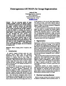
have been shown to be ideal materials for photodetection with significantly higher sensitivities than their bulk counterparts, arising from their high surface area-to-volume ratio that results in high density of surface states (21, 33). The surface states trap the photogenerated holes and, therefore, effectively increase the electron carrier lifetime that results in the enhancement of the photocurrent (21). To implement CdSe NWs as optical sensors, Schottky devices were fabricated by contacting the NWs with high work function Ni/Pd (5/45 nm) source (S) and drain (D) electrodes (Fig. 1A). NWs were grown intrinsically without any intentional doping by using the previously reported vapor– liquid–solid process (see Methods; 34), and as expected they exhibited n-type behavior (Fig. 1B) because of their surface Fermi level pinning. From photoluminescence measurements, a band gap of ⬇1.76 eV was extracted (see supporting information (SI) Fig. S1), which is consistent with the reported bulk value, and is indicative of stoichiometric composition. The electrical characteristic of a representative CdSe NW Schottky device is shown in Fig. 1B. The device exhibits large dark resistance Rdark ⬇140 G⍀ because of the Schottky barriers at the S/D interfaces that severely limit the carrier injection from the metal into the chemically intrinsic semiconductor NWs. On white light illumination (halogen light source, 4.4 mW/cm2), a drastic decrease of ⬇100 times in the device resistance (Rlight ⬇2 G⍀) is observed that is attributed to the efficient electron/hole photogeneration and field-induced carrier separation in CdSe NWs (Fig. 1 A). The photocurrent gain in our NW devices is comparable to the best reported values in literature for physical vapor-deposited CdSe thin films. However, for such thin-film devices, the exact gain (ranging from 10 to 1,000 times for ⬇80 mW/cm2 illumination) is shown to highly depend on the annealing and deposition temperature conditions that effectively control the film stoichiometry, morphology, and crystallinity (35). In distinct contrast, NWs are single crystalline with controlled composition, and require only ambient temperature processing for their deposition (i.e., assembly) on substrates, making them highly compatible with a wide range of substrates, including plastics and papers. To further characterize the CdSe NW photosensors, transient and illumination intensity-dependent measurements were performed. Time-resolved photoresponse measurements were conducted for multiple illumination cycles as depicted in Fig. 1C. Each photoresponse cycle consists of three transient regimes—a sharp rise ( ⬇0.7 sec), steady state, and sharp decay ( ⬇0.7 sec). We note that our time constants are larger than the best reported values for nanowires in the literature (21, 33). We attribute this Author contributions: Z.F., J.C.H., Z.A.J., H.R., and A.J. designed research; Z.F., J.C.H., Z.A.J., and H.R. performed research; Z.F., J.C.H., Z.A.J., H.R., and A.J. analyzed data; and Z.F., J.C.H., Z.A.J., H.R., and A.J. wrote the paper. The authors declare no conflict of interest. This article is a PNAS Direct Submission. ‡Z.F. §To
and J.C.H. contributed equally to this work.
whom correspondence should be addressed. E-mail:
[email protected].
This article contains supporting information online at www.pnas.org/cgi/content/full/ 0801994105/DCSupplemental. © 2008 by The National Academy of Sciences of the USA
www.pnas.org兾cgi兾doi兾10.1073兾pnas.0801994105
10
S (Ni/Pd)
D (Ni/Pd)
10 IDS (nA)
5µm
0
B
VDS = 2V
-1
10
-2
10
-3
10
-4
0
VGS = 0V
10 IDS (nA)
A
-1
10
-2
10
-3
10
-2
-10
V
0
GS
10
0
C
1.2
VDS = 2V
IDS (nA)
IDS (nA)
(V)
0 1 VDS (V)
2
10
VDS = 2V
1.0
6 4 2
10
D
-1
-1 6 4
0.8 0.6 0.4 0.2
2
0
100 200 Time (sec)
0
4 8 12 2 Intensity (mW/cm )
to (i) the quality of our nanowires, which can be readily improved in the future through growth optimization, and (ii) the measurement setup. However, this response time is adequate for the purpose of this work, and in principle it can be drastically improved in the future, if desired. Importantly, a nearly identical response is observed for multiple cycles which demonstrates the robustness and reproducibility of the NW optical sensors. The illumination power dependence of the photoresponse is shown in Fig. 1D, exhibiting two distinct regimes with the transition intensity of ⬇2mW/cm2. This nonlinear photoresponse has also been reported in other NW photodetectors, and has been attributed to the charge-trapping and recombination processes due to the dominant surface states in the forbidden gap of NWs (35, 36). Although the miniaturized nanosensor elements, such as the CdSe NW photodetectors shown here, provide high sensitivity to the environment with high spatial resolution, they are inherently limited to low signal amplitude (i.e., current), and therefore require an eventual signal amplification via electronic circuitry to enable effective data processing. To date, this important requirement has not yet been addressed. Here, we report direct, on-chip amplification of the nanosensor signal by using an all-NW circuitry without any external wiring. The schematic, SEM, and optical images of a fabricated all-nanowire circuit is shown in Fig. 2, consisting of three active device elements: (i) optical nanosensors (NSs) based on either a single or parallel arrays of multiple CdSe NWs, (ii) a high-resistance field-effect transistor (FET) (T1) based on parallel arrays of 1–5 Ge/Si core/shell NWs, and (iii) a low-resistance buffer FET (T2) with the channel consisting of parallel arrays of ⬇2,000 NWs. The Fan et al.
all-nanowire circuitry utilizes T1 to match the output impedance of the NS in a voltage divider configuration. Once the illumination-dependent NS current is translated into potential VG2, the output current of T2 is modulated according to its transfer characteristics, resulting in ⬇5 orders of magnitude amplification of the NS current signal. To enable the successful fabrication of the all-integrated, heterogeneous NW circuitry, it is essential to assemble highly regular NW arrays with high uniformity at well defined locations on the substrate. Recently, we have developed a contact printing technology for direct transfer of highly ordered and aligned NW arrays on various receiver substrates with high reproducibility over large areas (29, 30). In this approach, a dense ‘‘lawn’’ of single crystalline NWs with controlled composition is first grown on a growth substrate by using the vapor–liquid–solid process, followed by the transfer of NWs to a receiver substrate by a directional sliding. Before the printing process, the receiver substrate is coated with a photolithographically patterned resist layer that enables for patterned NW assembly on resist removal in acetone. We incorporated this assembly approach for enabling the fabrication of the all-nanowire sensor circuitry. First, highly aligned CdSe and Ge/Si NW arrays were assembled at predefined locations on a Si/SiO2 (50 nm, thermally grown) substrate by using a two-step printing process (see Methods). Ni/Pd S/D electrodes were then patterned on NW arrays followed by atomic layer deposition (ALD) of 8- to 9-nm-thick HfO2 film as the high- gate dielectric. Finally, the HfO2 layer was selectively etched in hydrofluoric acid at the bonding pads and vias, and the top gate electrodes (Ni/Pd) were patterned on Ge/Si NWs while simultaneously forming the vias between the two metal layers PNAS 兩 August 12, 2008 兩 vol. 105 兩 no. 32 兩 11067
ENGINEERING
Fig. 1. Highly sensitive, direct band-gap NW photodiodes. (A) SEM (Top), schematic (Middle), and the band diagram (Bottom) of a CdSe NW photodetector with Ni/Pd Schottky S/D contacts. (B) IDS-VGS and IDS-VDS (Inset) curves of a representative CdSe NW device before (dashed, gray line) and after (solid, red line) white light illumination, exhibiting ⬇100 times the current modulation. (C) Transient of a single CdSe NW device with an illumination intensity of 4.4 mW/cm2. (D) Illumination intensity-dependent measurements of a CdSe NW device, showing a nonlinear behavior.
A 100
A
IDS (mA)
10
T2
10
-3
10
-4
10
-5
-1
T1
10
-2
10
-3
-2
0 VGS (V)
2
B 300
-1.5
-Iout (µA)
B
VG2 (V)
-1.0
200
-0.5
100
C2
NS T2 T1
C3
C4
300
300
T1
T2
10µm
100 200 Time (sec)
C
4µm 100 µm
0
NS
Iout (µA)
C1
0.0
200
4µm
Fig. 2. Heterogeneous NW assembly for an all integrated, sensor circuitry. (A) Circuit diagram for the all-nanowire photodetector, with high-mobility Ge/Si NW FETs (T1 and T2) amplifying the photoresponse of a CdSe nanosensor. (B) Schematic of the all-nanowire optical sensor circuit based on ordered arrays of Ge/Si and CdSe NWs. (C1) An optical image of the fabricated NW circuitry, consisting of a CdSe nanosensor [NS (C2)] and two Ge/Si core/shell NW FETs [T2 and T1, (C3) and (C4)] with channel widths ⬇300 m and 1 m, respectively. Each device element within the circuit can be independently addressed for dynamics studies and circuit debugging.
(see Methods). Fig. 2C shows an optical microscopy image of a fabricated circuit and scanning electron microscopy (SEM) images of each individual component, clearly demonstrating the highly ordered NW positioning and the on-chip integration. The achieved NW alignment is highly desirable for high-performance and highly uniform transistor and sensor arrays. For transistors, a high degree of alignment, without NW crossing, is needed to reduce variation in gate electrostatics coupling and NW channel length, both of which directly affect the switching performance. Similarly, for CdSe optical sensors, the alignment is critical for uniform response of the devices, but also more uniquely to enable well defined polarized sensitivity that arises from the 1D nature of NWs (18). The polarization-dependent photoconduction measurements of single and parallel arrays of CdSe NWs are depicted in Fig. S2. In particular, near-identical polarizationdependent response is observed for various printed CdSe NWs with similar minima and maxima polarization angles, which further illustrates the highly aligned assembly of NWs by contact printing. This is in distinct contrast to the randomly aligned NWs assembled by the drop-casting method that show different polarized response depending on the orientation of the particular wire. 11068 兩 www.pnas.org兾cgi兾doi兾10.1073兾pnas.0801994105
100 0
5 10 2 Intensity (mW/cm )
Fig. 3. All-integrated NW sensor circuitry. (A) Transfer characteristics of parallel array Ge/Si NW FETs with channel width of ⬇1 m (dashed line, T1) and ⬇300 m (solid line, T2) with VDS ⫽ 3V. The blue box represents the active operation regime in which the photosensor circuit is being operated. (B) Circuit output current (blue curve) and voltage divider output voltage (gray curve) response to light illumination (4.4 mW/cm2). (C) Light-intensitydependent measurement of the circuit output current.
The all-nanowire photosensor circuits were measured at both the single-device component and circuit levels to characterize their operational performance. Fig. 3A shows the transfer characteristics of T1 and T2, both exhibiting clear p-type switching characteristics with ION ⬇4 A and 1 mA, respectively. Further detailed characterization of representative Ge/Si NWs FETs is presented in Fig. S3. In summary, the Ge/Si NW FETs showed minimal hysteresis (⬍200 mV) owing to the passivation from the environment (i.e., humidity) by the top gate stacks, and the high-quality gate dielectrics deposited by ALD (38). A hole mobility range of p ⫽ 30–120 cm2/V䡠s is extracted from the standard square law model (Fig. S3D). Although the highest p of our NWs is comparable to that of Si p-metal oxide semiconductor FETs, the mobility is ⬇7 times lower than the best reported value for Ge/Si NW FETs (9, 37). We attribute this to the nonideal high-/NW interfaces and/or non-ohmic metal contacts in our fabricated device structures. Ge/Si NW FETs were found nonresponsive to white light illumination which guaranteed no undesired interference (see Fig. S4). For the circuit level operation, the operating bias, VDD was maintained at ⫺3V for all measurements. The gate electrode Fan et al.
A
B
1 mm
Number of Circuits
60
C
4.4 mW/cm2
D
40
20
0
0
200 400 600 800 Photocurrent (µA)
2 mm
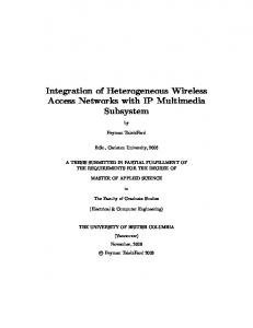
for T1 was biased at VG1 ⫽ 3V (corresponding to RT1 ⫽ 1–2 G⍀) to match the output impedance of the CdSe NS. The output signal of a circuit for multiple white light illumination cycles (4.4 mW/cm2) is depicted in Fig. 3B, showing average dark and light currents of ⬇80 A and ⬇300 A, respectively. Importantly, this output current is quantitatively consistent with the value that is estimated based on the circuit layout and the electrical properties of the single-device components. The output current of the circuit can be estimated from the transfer characteristics of T2 and the output voltage of the voltage divider, which is also the input to T2. The output of the voltage divider, VG2 can be estimated as VG2 ⫽ VDD ⫻ RT1/(RT1 ⫹ RNS), corresponding to VG2 ⬇ ⫺0.02V and ⫺1.11V for dark and light (RNS-dark ⬇140 G⍀ and RNS-light ⬇2 G⍀; Fig. 1B) scenarios, respectively, which is in good agreement with the measurements (blue curve, Fig. 3B). The VG2 swing defines the operation regime of T2 as depicted in the transfer characteristics (Fig. 3A). This operation regime corresponds to an output current swing of 87–310 A, consistent with the measured values and the PSpice modeling (see Fig. S5). The intensity-dependent photoresponse measurements were conducted as shown in Fig. 3C to further characterize the integrated circuits. The trend is nearly identical to the photoresponse of the single CdSe NW device (Fig. 1D), suggesting that the signal amplification by the circuit is nearly linear for the illumination intensity of 0–13 mW/cm2. The circuit level measurements demonstrate the successful operation of NW circuits for effective amplification of the small photocurrent generated by the NS elements. To further demonstrate the versatility of our approach, we fabricated large arrays (i.e., 13 ⫻ 20) of the all-nanowire circuits on a chip (Fig. 4A), and measured the photoresponse of each individual circuit element. Rather than single CdSe NWs, parallel arrays of 5–10 NWs were used as the active element of each Fan et al.
NS to enhance the yield and reduce the variation by taking advantage of the averaging effect (see Fig. S6). It was found that ⬇80% of the circuits demonstrated successful photoresponse operation as depicted in the failure analysis map (Fig. 4B). The functional circuits exhibited a mean photocurrent of ⬇420 A with a standard deviation of ⫾165 A. The reasonably small circuit-to-circuit variation arises from the uniformity of the assembled nanowire arrays. The three major causes for circuit failure were (i) fabrication defects (i.e., poor metal lift-off and gate dielectric breakdown), (ii) failed CdSe printing, and (iii) weak photoresponse from CdSe NWs (i.e., defective NWs), which represent ⬇10%, 5%, and 5% of the fabricated circuits accordingly. The high yield of the operational circuits with a high level of complexity proves the potential of the NW technology and our parallel array assembly approach for large-scale sensor and electronic integration. In the future, this yield can be further enhanced through NW synthesis and fabrication-processing optimization. The large NW circuit matrix can readily function as an image sensor. To demonstrate this feasibility, as a proof of concept, a halogen light source was focused and projected onto the center of the matrix. The output current was measured for each individual working circuit and digitized into a 0–100 scale with ‘‘0’’ and ‘‘100’’ representing the maximum and minimum measured intensity, respectively (see SI Text). Each of the circuits was regarded as a pixel and the measured intensity levels of the circuits were incorporated into a 2D plot to generate a contrast map shown in Fig. 4D. The contrast map clearly demonstrates the spatial intensity variation from the center to the outer edge of the circuit matrix, precisely matching the intensity profile of the projected light source, thus showing a preliminary imaging function with an all-nanowire circuit array. In future, significant downscaling of the pixel size can be achieved by reducing the PNAS 兩 August 12, 2008 兩 vol. 105 兩 no. 32 兩 11069
ENGINEERING
Fig. 4. Large-scale and heterogeneous integration of NWs for image sensing. (A) Optical image of an array of all-nanowire photodetector circuitry with each circuit element serving as an independently addressable pixel. (B) A defect analysis map showing the functional and defective NW photodetector circuit elements. (C) A histogram of the photocurrent for all functional circuit elements of the fabricated array. (D) An output response of the circuit array, imaging a circular light spot. The contrast represents the normalized photocurrent, with the gray pixels representing the defective sites (see SI Text).
feature size (for instance, channel length and width) of the Ge/Si NW FETs and the metal interconnects. In summary, the large-scale assembly of NWs for heterogeneous, sensor circuitry with on-chip integration was demonstrated. The sensory and electronic functionalities of NWs have been interfaced through heterogeneous integration of direct band gap CdSe NWs and high-mobility Ge/Si NWs. Active elements consisting of both single and parallel arrays of NWs were incorporated to enable the circuit operation, involving 5 orders of magnitude current amplification of the nanosensor’s signal. Importantly, by using parallel arrays of NWs as the active component of each device, the reliability and uniformity was significantly enhanced, therefore, enabling a reliable large-scale integration path for the demonstration of an image sensor. In the future, the process can be expanded to other optically active NWs, which combined with the scaling of the fabricated devices may enable high-resolution and multicolor imaging. This work not only demonstrates the nanowire device integration at an unprecedented scale, but also illustrates and presents a system based on printed NW arrays that may enable a number of technological applications by using NWs as the building blocks. Methods Nanowire Growth. Ge/Si core/shell NW growth process can be found in ref. 9. CdSe nanowires were grown in a custom-made CVD system with a single zone, resistive heating furnace (Lindburg Blue), which accommodates one-inch diameter quartz tubes. Gold nanoparticles with 30-nm diameter were deposited on Si/SiO2 substrates and served as catalysts for the vapor–liquid–solid growth process. Before the growth, 1.5 g of CdSe powder (Alfa Aesar, 99.999%) was placed in a quartz boat and loaded into the center of the heating zone in the furnace. Then, the growth substrate was placed at the downstream, ⬇9.5 cm away from the center of the furnace. The nanowire growth was carried out with the furnace temperature (precursor tempera-
1. Lieber CM, Wang ZL (2007) Functional nanowires. MRS Bull 32:99 –108. 2. Lieber CM (2003) Nanoscale science and technology: Building a big future from small things. MRS Bull 28:486 – 491. 3. Avouris, P. Chen J (2006) Nanotube electronics and optoelectronics. Mater Today 9:46 –54. 4. McEuen PL (2000) Single-wall carbon nanotubes. Phys World 13:31–36. 5. Rogers JA (2007) Slice and dice, peel and stick: Emerging methods for nanostructure fabrication. ACS Nano 1:151–153. 6. Bryllert T, Wernersson LE, Froberg LE, Samuelson L (2006) Vertical high-mobility wrap-gated InAs nanowire transistor. IEEE Electron Device Lett 27:323–325. 7. Javey A, Nam S, Friendman RS, Yan H, Lieber CM (2007) Layer-by-layer assembly of nanowires for three-dimensional, multifunctional electronics. Nano Lett 7:773–777. 8. Javey A, Guo J, Wang Q, Lundstrom M, Dai HJ (2003) Ballistic carbon nanotube transistors. Nature 424:654 – 657. 9. Xiang J, et al. (2006) Ge/Si nanowire heterostructures on high-performance field-effect transistors. Nature 441:489 – 493. 10. Ahn, J. H., et al. (2006) Heterogeneous three-dimensional electronics by use of printed semiconductor nanomaterials. Science 314:1754 –1757. 11. Chen ZH, et al. (2006) An integrated logic circuit assembled on a single carbon nanotube. Science 311:1735. 12. Kang SJ, et al. (2007) Printed multilayer superstructures of aligned single-walled carbon nanotubes for electronic applications. Nano Lett 7:3343–3348. 13. Kang SJ, et al. (2007) High-performance electronics using dense, perfectly aligned arrays of single-walled carbon nanotubes. Nature Nanotech 2:230 –236. 14. Bachtold A, Hadley P, Nakanishi T, Dekker C (2001) Logic circuits with carbon nanotube transistors. Science 294:1317–1320. 15. Wang D, Sheriff B, Heath JR (2006) Complementary symmetry silicon nanowire logic: Power-efficient inverters with gain. Small 2:1153–1158. 16. Ju S, et al. (2007) Fabrication of fully transparent nanowire transistors for transparent and flexible electronics. Nat Nanotech 2:378 –384. 17. Friedman RS, McAlpine MC, Ricketts DS, Ham D, Lieber CM (2005) High-speed integrated nanowire circuits. Nature 434:1085. 18. Wang J, Gudiksen MS, Duan X, Cui Y, Lieber CM (2001) Highly polarized photoluminescence and photodetection from single indium phosphide nanowires. Science 293:1455–1457. 19. Tian B, et al. (2007) Coaxial silicon nanowires as solar cells and nanoelectronic power sources. Nature 449:885– 889. 20. Lewis NS (2007) Toward cost-effective solar energy use. Science 315:798 – 801.
11070 兩 www.pnas.org兾cgi兾doi兾10.1073兾pnas.0801994105
ture) at 700°C and 50 standard cubic centimeters per minute continuous flow of hydrogen. The system pressure was stabilized at 30 torr with a pressure controller and the growth was carried out for 1.5 h. Nanowire Contact Printing. An alignment mark layer was first created on a Si/SiO2 substrate. Then a layer of photoresist (Shipley 1805 diluted in propylene glycol monomethyl ether acetate with 1:3 volume ratio) was spincoated on the substrate, and lithographically patterned to define printing channels for the CdSe nanowire assembly. The details of the printing process can be found in ref. 29. After CdSe nanowire printing, the photoresist was removed in acetone followed by a second printing step for Ge/Si nanowires by using an identical process flow. Device Fabrication. After contact printing of CdSe and Ge/Si nanowires, sourcedrain contact electrodes were patterned with photolithography. Then Ni (5 nm)/Pd (45 nm) was evaporated with an electron beam evaporator followed by lift-off. HfO2 high- gate dielectric film was then deposited by using an atomic layer deposition tool. In this process, tetrakis(dimethylamino) hafnium maintained at 110°C and water were used as the precursors. HfO2 was deposited for 85 cycles (⬇9 nm thick) at 140°C, with each cycle consisting of a 1-sec tetrakis(dimethylamino) hafnium precursor pulse, 20-sec nitrogen purge, 1-sec water vapor pulse, and 40-sec nitrogen purge. Thereafter, etching windows on source-drain bonding pads and the bridges (vias) between the Ge/Si transistors were photolithographically patterned, and the HfO2 was chemically etched with 5% HF for 35 sec. Finally, Ni (5 nm)/Pd (45 nm) for the top metal gate electrodes of T1 and T2, and the vias were fabricated by photolithography, metallization, and lift-off. ACKNOWLEDGMENTS. We thank A. M. Peczalski for insightful discussions, and Professor M. Wu and Dr. K. Yu for help with optical measurements. All fabrication was performed in the Berkeley Microfabrication Laboratory. This work was supported by Defense Advanced Research Projects Agency/ Microsystems Technology Office, Intel, and Materials Structures and Device Focus Center. The nanowire synthesis was supported by a Laboratory Directed Research and Development Project from Lawrence Berkeley National Laboratory. J.C.H received a graduate fellowship from Intel Foundation.
21. Soci C, et al. (2007) ZnO nanowire UV photodetectors with high internal gain. Nano Lett 7:1003–1009. 22. Cui Y, Wei Q, Park H, Lieber CM (2001) Nanowire nanosensors for highly sensitive and selective detection of biological and chemical species. Science 293:1289 –1292. 23. Patolsky F, et al. (2006) Detection, stimulation, and inhibition of neuronal signals with high-density nanowire transistor arrays. Science 313:1100 –1104. 24. McAlpine MC, Ahmad H, Wang D, Heath JR (2007) Highly ordered nanowire arrays on plastic substrates for ultrasensitive flexible chemical sensors. Nat Mater 6:379 –384. 25. Zhang DH, et al. (2004) Detection of NO2 down to ppb levels using individual and multiple In2O3 nanowire devices. Nano Lett 4:1919 –1924. 26. Stern E, et al. (2007) Label-free immunodetection with CMOS-compatible semiconducting nanowires. Nature 445:519 –522. 27. Wang ZL, Song J (2006) Piezoelectric nanogenerators based on zinc oxide nanowire arrays. Science 312:242–246. 28. Ju S, et al. (2008) Transparent active matrix organic light-emitting diode displays driven by nanowire transistor circuitry. Nano Lett 8:997–1004. 29. Fan Z, et al. (2008) Wafer-scale assembly of highly ordered semiconductor nanowire arrays by contact printing. Nano Lett 8:20 –25. 30. Yerushalmi R, Jacobson ZA, Ho JC, Fan Z, Javey A (2007) Large scale, highly ordered assembly of nanowire parallel arrays by differential roll printing. Appl Phys Lett 91:203104. 31. Chan EM, Mathies RA, Alivisatos AP (2003) Size-controlled growth of CdSe nanocrystals in microfluidic reactors. Nano Lett 3:199 –201. 32. Gudiksen MS, Maher KN, Ouyang L, Park H (2005) Electroluminescence from a singlenanocrystal transistor. Nano Lett 5:2257–2261. 33. Jie JS, et al. (2006) Photoconductive characteristics of single-crystal CdS nanoribbons. Nano Lett 6:1887–1892. 34. Ma C, Wang ZL (2005) Road map for the controlled synthesis of cdse nanowires, nanobelts, and nanosaws—A step towards nanomanufacturing. Adv Mater 17:2635–2639. 35. Raturi AK, Thankaraj R, Sharma AK, Tripathi BB, Agnihotri OP (1982) Structural, optical, and photoconducting properties of sprayed CdSe Films. Thin Solid Films 91:55– 64. 36. Rose A (1963) Concepts in Photoconductivity and Allied Problems (Interscience, New York). 37. Hu Y, Xiang J, Liang G, Yan H, Lieber CM (2008) Sub-100 nanometer channel length Ge/Si nanowire transistors with potential for 2 THz switching speed. Nano Lett 8:925– 930. 38. Javey A, et al. (2002) High-k dielectrics for advanced carbon nanotube transistors and logic. Nat Mater 1:241–246.
Fan et al.