Jan 11, 2010 - §Intel Corporation, Santa Clara, CA. ABSTRACT ... technologies such as microelectromechanical systems (MEMS) and various kinds of ...
Layout-Driven Test-Architecture Design and Optimization for 3D SoCs under Pre-Bond Test-Pin-Count Constraint Li Jiang†∗ , Qiang Xu†∗ , Krishnendu Chakrabarty‡ , and T. M. Mak§ † Deptartment of CS&E, The Chinese University of Hong Kong, Shatin, N.T., Hong ∗ CAS-CUHK Shenzhen Institute of Advanced Integration Technology ‡ Deptartment
Kong
of ECE, Duke University, Durham, NC Corporation, Santa Clara, CA
§ Intel
ABSTRACT We propose a layout-driven test-architecture design and optimization technique for core-based system-on-chips (SoCs) that are fabricated using three-dimensional (3D) integration. In contrast to prior work, we consider the pre-bond test-pin-count constraint during optimization since these pins occupy large silicon area that cannot be used in functional mode. In addition, the proposed test-architecture design takes the SoC layout into consideration and facilitates the sharing of test wires between pre-bond tests and post-bond test, which significantly reduces the routing cost for a test-access mechanism in 3D technology. Experimental results for the ITC’02 SoC benchmarks circuits demonstrate the effectiveness of the proposed solution.
1. INTRODUCTION As system-on-a-chip (SoC) designs become increasingly complex, interconnects have emerged as the performance and power limiter for giga-scale integrated circuits (ICs). Three-dimensional (3D) technology is able to provide abundant interconnect resources with improved performance and less communication energy by integrating multiple silicon dies with short and dense through-silicon vias (TSVs). As a result, it has become a promising solution to address the interconnect problem [3]. 3D technology also facilitates the integration of disparate technologies such as microelectromechanical systems (MEMS) and various kinds of sensors as they can be fabricated on different silicon layers separately before integration, thereby offering a genuine single-chip system solution. Because of the above benefits, industry experts predict that 3D ICs will occupy a big market share for future semiconductor products [21], despite the still unresolved testing and thermal-management challenges. In 3D ICs, silicon dies at different layers can be built in three ways: wafer-to-wafer (W2W) bonding [19], die-to-die (D2D) bonding [13], or die-to-wafer (D2W) bonding (for 3D ICs built on two semiconductor wafers only) [4]. Known good dies (KGDs) can be attached through pre-bond wafer-level testing to achieve higher manufacturing yield in D2D bonding or D2W bonding [3, 15]. Therefore, when the die size is large and/or the defect density is high, they are preferred over W2W bonding. In terms of bonding direction, there can be faceto-face bonding or face-to-back bonding. The former allows more interconnects between active devices on different layers but it limits the number of stacked dies to be two; the latter is a scalable solution that supports more stacking layers. Permission to make digital or hard copies of all or part of this work for personal or classroom use is granted without fee provided that copies are not made or distributed for profit or commercial advantage and that copies bear this notice and the full citation on the first page. To copy otherwise, or republish, to post on servers or to redistribute to lists, requires prior specific permission and/or a fee. ICCAD’09, November 2–5, 2009, San Jose, California, USA. Copyright 2009 ACM 978-1-60558-800-1/09/11...$10.00.
In order to enable pre-bond tests and improve manufacturing yield for 3D ICs, we need to fabricate a number of test pads on the silicon die so that the automatic test equipment (ATE) can probe it during testing. The test pads, however, occupy much larger area compared to the TSVs. Typically, one single test pad can consume area equivalent to hundreds of front-side vias. Therefore, if a large number of test pads are fabricated, the benefits of exploiting TSVs for interconnecting active devices between layers are significantly reduced. As a result, it is essential to take the pre-bond test-pin-count constraint into consideration during test planning. Related prior work in test architecture design and optimization for 3D SoCs [8], however, tries to integrate pre-bond tests and post-bond test together and may lead to high test pad requirement for certain dies. To tackle the above problem, in this work, we design test architectures for pre-bond tests and post-bond test separately so that the testpin-count constraint can be satisfied in pre-bond tests. By doing so, however, the routing cost for test access mechanisms (TAMs) may be dramatically increased as pre-bond tests and post-bond test have different TAMs. To address this issue, we propose optimization methods that allow us to share routing resources between pre-bond tests and post-bond test as much as possible. Also, we show how to optimize test architectures to further reduce TAM routing cost with little impact on testing time. Experimental results on several 3D adaptations of the ITC’02 benchmark circuits show that, the proposed layout-driven test architecture design and optimization techniques for 3D SoCs can reduce TAM wire length by up to 50% with only a small increase in testing time. The remainder of this paper is organized as follows. Section 2 reviews related work and motivates this paper. The problem investigated in this paper is then formulated in Section 3. Next, our proposed layout-driven test architecture design and optimization techniques are detailed in Section 4. Section 5 presents experimental results to show the advantages of the proposed method. Finally, Section 6 concludes this paper.
2. PRELIMINARIES AND MOTIVATION 2.1 Prior Work in Testing 3D ICs Test techniques and design-for-testability (DfT) solutions for 3D ICs are critical issues for the success of 3D technology, as pointed out in [14, 16]. However, only limited work has been done in this emerging area. Lewis and Lee [12] proposed a scan-island-based design to enable pre-bond tests for incomplete circuits at the architecture level. Wu et al. [18] studied several scan chain design approaches for 3D ICs and compared their routing costs. The above works mainly target 3D ICs that put functional blocks in different silicon layers. For 3D SoCs with entire embedded cores on different layers, modular testing is an attractive solution as it facilitates the reuse of test patterns. While test architecture design and optimization for twodimensional SoCs have been subject to extensive research [20], these solutions are not readily applicable for testing 3D SoCs. Recently, a test-access mechanism (TAM) optimization technique was proposed
191
Authorized licensed use limited to: DUKE UNIVERSITY. Downloaded on January 11, 2010 at 12:31 from IEEE Xplore. Restrictions apply.
Post-bond TAM ID Cu Cu
TSV
C4 Bump
Cu
Bond Pad
Cu
Bulk Si (b)
(a)
TP1
Layer 2
W3 8 TP4
TP2 17 3 6 Legend
W1 4 W2
TSV
2 5
TPi : Test Pad i TAM_2
TAM_1 TAM_3
Figure 2: Test architecture for an example 3D SoC. in [17] to minimize the testing time of 3D SOCs, under limits on the number of TSVs utilized by TAMs. However, pre-bond tests were not considered in this work and hence it can only provide cost-effective solutions for 3D SoCs manufactured with W2W bonding technology. Jiang et al. [8] proposed simulated annealing (SA) based algorithms to optimize modular SoC test architecture considering both pre-bond tests and post-bond test. In this work, the same TAMs that traverse multiple layers in post-bond testing are fully reused for pre-bond tests. Consequently, TAMs can be divided into multiple parts and distributed among the different silicon layers. As all the TAM segments in a particular silicon layer need to be probed during pre-bond testing, a large amount of test pads may be required for those silicon dies that contain many TAM segments. This can be a serious issue in pre-bond testing, as shown in the following section.
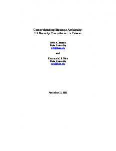
2.2 Test-Pin-Count Constraint When conducting pre-bond tests for silicon dies at wafer-level, one of the biggest challenges is how to probe the silicon die effectively. As shown in [1], since fine-grained touchdown probe needles are not available in the next decade, producing dense probe arrays to connect to the ATE is not a viable solution, at least for the near future. Consequently, we have to fabricate test pads (C4 bump or wire bond, see Fig. 1) on silicon dies and rely on conventional probing techniques to connect them to the ATE during pre-bond testing [14]. At the same time, however, it is not possible to fabricate a large number of test pads for pre-bond testing in 3D ICs. This is because of the following reasons. According to [1], the pitch for C4 bumps is around 120μm, which is much larger than that of TSV (1.7μm as shown in [22] and this figure keeps shrinking with technology improvements). In other words, one single test pad can consume area equivalent to hundreds of TSVs (see Fig. 1). As these test pads have to be put at the “keep-out area” for TSVs (i.e., TSVs need to keep some distance from any other component), the benefits of exploiting dense TSVs for interconnecting active devices between layers are significantly diminished with the increase of test pads [11]. In 3D technology, except for the bottom layer, the silicon bulks in other layers are thinned for the ease of TSV fabrication. If we conduct pre-bond tests before thinning, we may not be able to detect the failures introduced during the chemical mechanical polishing (CMP) process. If, however, we probe the thinned wafer instead, the probe force (typically 3 − 10g per probe and 60 − 120kg per wafer) during testing becomes a serious concern as these thinned wafers are not mechanically strong enough. Again, it is desired to have less test pads (probes/touchdowns) for silicon dies in pre-bond testing.
192
Pre-bond Test Pad
W1 C8 4,1 C5 2,2
Pad
C7 4,1 w4
C4 2,2
C9 3,1 C10 3,2
w2
C8 4,1 C5 2,2
(b)
Figure 3: Routing resource sharing example: (a) Test Architecture During Post-bond Test, (b) Reuse TAM During Pre-bond Test.
2.3
7
11
TP6
W2 C4 2,2
C2 1,1
w1 C3 1,2
TP5
9
10 7
C1 1,1
(a)
Figure 1: Pre-bond Test Pad: (a) C4 Bump as Test Pad, (b) WireBond as Test Pad.
TP3
C10 3,2
Bulk Si
C9 3,1
Pre-bond TAM ID
C7 4,1
C3 1,2
TSV
Layer 1
C2 1,1
C1 1,1
Device Layer
Core ID
Motivation
The most straightforward solution to take pre-bond test-pin-count constraint into consideration during the 3D SoC test architecture design and optimization process is to design separate test architectures for pre-bond tests and post-bond test. By doing so, however, the total TAM routing cost for 3D SoCs can be quite high as we have dedicated TAMs for pre-bond tests, resulting in degradation of the chip’s routability. As we need to link cores using both pre-bond TAMs and post-bond TAMs and they are used at different times, a natural question is whether we can share some of the routing resources between the two types of TAMs. We use the following example to demonstrate the possibility of sharing routing resources and its potential benefits. Consider a twolayer 3D SoC containing 11 cores, in which six of them (C1 to C6) are on the bottom layer while the other five cores (C7 to C11) are on the top layer. Similar to [8], for the sake of TSV count consideration, we assume a post-bond TAM involved in several layers will route through all cores tested with this TAM on one layer before it goes through TSVs to connect cores in other layers. In this example 3D SoC, three TAMs are used for post-bond testing and they are shown in Fig. 2. As an example, TAM1 connects C1, C2, C7, C8, and C9 with TAM width W 1, starting from test pad T P1 and ending at test pad T P2 . For the ease of discussion, we map a few cores in the 3D SoC onto one layer as shown in Fig. 3(a). In this figure, each vertex represents a core, in which the upper label is the core ID, while the lower one denotes the pre-bond TAM ID and post-bond TAM ID that this core belongs to. In Fig. 3(b), we show how pre-bond TAMs can reuse the existing test wires for post-bond testing, wherein the solid lines are pre-bond TAMs. It can be easily observed that those wires having both solid and dashed/doted lines can be shared between pre-bond test and post-bond test, which can significantly reduce the total routing cost for TAMs in 3D SoCs. Note that, during pre-bond test, the end points of each TAM are directly routed to deliver test data on its own silicon layer. Here, we assume that these test pad is near the end point, so that we can ignore the distance between end points and test pads. Obviously, some design-for-testability (DfT) circuitries need to be introduced to enable the routing resource sharing between pre-bond test and post-bond. To be specific, we need: (i) certain multiplexers to select the different test data source for pre-bond test and post-bond test (see the “×" point shown in Fig. 3(b)); (ii) reconfigurable test wrappers for cores that have different TAM width between pre-bond test and post-bond test (e.g., [9, 10]); (iii) the necessary control mechanisms (typically by introducing extra instructions in test wrapper and JTAG controller).
3.
PROBLEM FORMULATION
The layout-driven 3D SoC test architecture design and optimization problem investigated in this paper can be formulated as follows: Problem: Given • the set of cores C on the 3D SoC, and the test parameters for each core c ∈ C; • the layout of the 3D SoC, i.e., the physical position of every core c, including which layer it sits on and its X-Y coordinate on that layer;
2009 IEEE/ACM International Conference on Computer-Aided Design Digest of Technical Papers
Authorized licensed use limited to: DUKE UNIVERSITY. Downloaded on January 11, 2010 at 12:31 from IEEE Xplore. Restrictions apply.
∑
Wti × Lti
(1)
i=0
Here, Lti denotes the wire length for TAM ti , and we calculate it using the sum of Manhattan distance between adjacent cores in this TAM. When considering the sharing of pre-bond TAMs and post-bond TAMs, suppose the total length for the shared wires is Creused . The routing cost Croute becomes i