Nov 23, 2010 - Memory management in software development is supported by a rich ... Front Side Bus sockets and FPGAs connected to a host over a JTAG ...
Computer Science and Artificial Intelligence Laboratory Technical Report MIT-CSAIL-TR-2010-054
November 23, 2010
LEAP Scratchpads: Automatic Memory and Cache Management for Reconfigurable Logic [Extended Version] Michael Adler, Kermin E. Fleming, Angshuman Parashar, Michael Pellauer, and Joel Emer
m a ss a c h u se t t s i n st i t u t e o f t e c h n o l o g y, c a m b ri d g e , m a 02139 u s a — w w w. c s a il . m i t . e d u
LEAP Scratchpads: Automatic Memory and Cache Management for Reconfigurable Logic [Extended Version] ‡ Michael Adler† Kermin E. Fleming¶ Angshuman Parashar† Michael Pellauer¶ Joel Emer†¶ †
Intel Corporation VSSAD Group
¶
Massachusetts Institute of Technology Computer Science and A.I. Laboratory Computation Structures Group
{michael.adler, angshuman.parashar, joel.emer}@intel.com
{kfleming, pellauer, emer}@csail.mit.edu
ABSTRACT
1.
Developers accelerating applications on FPGAs or other reconfigurable logic have nothing but raw memory devices in their standard toolkits. Each project typically includes tedious development of single-use memory management. Software developers expect a programming environment to include automatic memory management. Virtual memory provides the illusion of very large arrays and processor caches reduce access latency without explicit programmer instructions. LEAP scratchpads for reconfigurable logic dynamically allocate and manage multiple, independent, memory arrays in a large backing store. Scratchpad accesses are cached automatically in multiple levels, ranging from shared on-board, RAM-based, set-associative caches to private caches stored in FPGA RAM blocks. In the LEAP framework, scratchpads share the same interface as on-die RAM blocks and are plug-in replacements. Additional libraries support heap management within a storage set. Like software developers, accelerator authors using scratchpads may focus more on core algorithms and less on memory management. Two uses of FPGA scratchpads are analyzed: buffer management in an H.264 decoder and memory management within a processor microarchitecture timing model.
FPGAs are increasingly employed as coprocessors alongside general purpose CPUs. The combination of large memory and ease of programming a general purpose machine along with the abundant parallelism and low communication latency in an FPGA make the pair attractive for hybrid algorithms that split computation across both engines. Memory management in software development is supported by a rich set of OS and library features. Describing overlays [6, 16], a method of swapping regions of code or data to fit in limited physical memory, elicits pitying chuckles from even well-educated computer scientists who began their careers after virtual memory became pervasive. Software designers targeting general purpose hardware long ago accepted that the gain in programmer efficiency from using compilers, support libraries and operating systems outweighs possible performance gains of hand-coding raw instructions. The memory subsystem in general purpose hardware offers a hierarchy of storage, ranging from fast but small caches embedded in the processor to large external RAM arrays on memory buses, and to swap files on disks. Management of cache state is controlled by fixed hardware algorithms chosen for their overall performance. Explicit, hand-tuned cache management instructions are typically added only to the most performance-sensitive programs. Tremendous effort has been spent building compilers capable of automatic cachemanagement, e.g. [12, 13]. As general purpose processors add more parallel processing, language designers continue to add abstract memory management to design tools in order to split algorithmic design from the grunt work of memory management [3]. The gap between the programming environment on the general purpose half and the reconfigurable half of a hybrid machine is stark. Most FPGA developers still code in low level languages equivalent to assembly language on general purpose machines. Those optimizing a set of loop kernels may use C or Java-like languages [8, 10, 11, 14] and a handful are beginning to use languages such as Bluespec [2, 19] that support language-based static elaboration and polymorphic module definitions. The state of memory management on reconfigurable logic is similarly primitive. FPGA synthesis tools support relatively easy management of on-die memory arrays. The interface to on-die RAM blocks is simple: a method for writing a value to an address and a two-phase pair of read request and response methods. This interface may be made timing insensitive by predicating the methods with ready and enable flags and
Categories and Subject Descriptors C.5.m [Computer System Implementation]: Miscellaneous
General Terms Algorithms, Performance
Keywords FPGA, memory management, caches
‡This is an extended version of a paper presented at FPGA 2011: Proceed-
ings of the 19th Annual ACM/SIGDA International Symposium on Field Programmable Gate Arrays (ISFPGA).
INTRODUCTION
buffering state on pipeline stalls [5].
1.1
Scratchpad memory hierarchies
What if an algorithm needs more memory than is available on-die? At best, designers are offered low-level device drivers for embedded memory controllers, PCIe DMA controllers or some other bus. Building an FPGA-side memory hierarchy is treated as an application-specific problem. Even methods for mapping memory management as basic as malloc and free to on-die RAM for C-like synthesis languages are a very recent innovation [22]. On general purpose hardware the memory hierarchy is invisible to an application, except for timing. A similar memory abstraction, identical to the interface to on-die RAM blocks but implementing a full storage hierarchy, is equally useful for a range of FPGA-based applications. Our project began as an effort to accelerate processor microarchitecture timing models using FPGAs. We quickly realized that some effort writing a general programming framework would make our task more tractable. The resulting platform is in active use for timing models and has been adopted for other algorithmic accelerators, such as an H.264 decoder. Both of these applications are considered in this paper. We have written LEAP (Logic-based Environment for Application Programming) [17], a platform for application development on reconfigurable logic. LEAP runs on any set of reconfigurable logic connected to general purpose machines. Like an operating system, LEAP is layered on top of devicespecific drivers. It presents a consistent virtual platform on any hardware. Application writers may then target the virtual platform, rendering their code portable across communication fabrics. LEAP presents the same interface over connections as diverse as FPGAs plugged directly into Intel Front Side Bus sockets and FPGAs connected to a host over a JTAG cable. The virtual platform provides a rich set of services, including streaming I/O devices, application control primitives, and an asynchronous hybrid procedural interface similar to remote procedure calls [18]. The platform also provides automatic instantiation of processor-like memory hierarchies, ranging from private caches, through shared caches and down to host memory. In this paper we focus on the automatically constructed memory stack. LEAP defines a single, timing insensitive, interface to scratchpad memory hierarchies. The same write, read request and read response interface methods are used for any memory implementation defined by the platform, along with the predicates governing whether the methods may be invoked in a given FPGA cycle. The simplest memory device allocates an on-die RAM block. However, LEAP memory stacks sharing the same interface can be configured for a variety of hierarchies. The most complicated has three levels: a large storage region such as virtual memory in a host system, a medium sized intermediate latency memory such as SDRAM controlled by an FPGA, and fast, small memories such as on-FPGA RAM blocks. Converting a client from using on-die memory to a complex memory hierarchy is simply a matter of instantiating a different memory module with identical connections. For a given set of hardware, low-level device drivers must be provided for each level in a physical hierarchy. Virtual devices and services are layered on top of these physical device drivers, thus providing a consistent programming model independent of the underlying physical devices. Our goal is
to make programming an FPGA more like software development on general purpose hardware. Programmers target an abstract set of virtual services similar to general purpose kernel and user-space libraries. Like general purpose hardware, programmers may get an algorithm working with generic code and then, optionally, tune their application for specific hardware latencies and sizes.
1.2
Related work
Many researchers have considered the problem of cache hierarchies in reconfigurable logic and embedded systems. Automatic generators build a variety of cache types and sizes, treating caches as building blocks [25]. Panda et al. presented an algoritm for computing application-specific cache hierarchies designed to minimize off-chip references [15]. CoRAM, a current research effort, is an investigation of application interfaces to memory hierarchies within reconfigurable logic [4]. CoRAM defines both a memory API and a control thread model for managing traffic between on-die and off-die memory. The CoRAM model could be implemented within the LEAP framework. LEAP scratchpads are a structured, hierarchical cache topology connected to applications through a relatively simple interface. In LEAP, the specific hierarchy instantiated is configurable from building blocks of both direct mapped and set associative caches. Clients may either accept the default private caches or may plug in their own, taking advantage of the sorts of access pattern optimizations considered in [15]. A CoRAM implementation within LEAP would replace the default, private, on-die cache with a CoRAM memory and control thread. Other projects, such as hthreads [1], have also built hybrid computation frameworks. Hthreads offers a hybrid pthreadsstyle thread management environment layered on coherent memory. The automatic instantiation of cached memory hierarchies we describe for LEAP scratchpads could be inserted into an hthreads stack as well.
2. 2.1
SCRATCHPAD ARCHITECTURE FPGA On-Die RAM Blocks
On-die FPGA RAM blocks can be configured quite flexibly. Xilinx RAM blocks are organized as 18Kb or 36Kb blocks in data widths of 1, 2, 4, 9, 18 or 36 bits [24]. Altera RAM blocks have similar widths. Synthesis tools automatically provide the illusion of arbitrary size and width by grouping multiple blocks into a single logical block and mapping into the closest available bit width. A large Xilinx Virtex 6 FPGA has about 32Mb of RAM. Access to RAM blocks is simple: a single cycle write operation and a two phase read request / read response protocol. Even a na¨ıve implementation can be dual ported, permitting simultaneous reads and writes. RAM blocks are fast, flexible and easy to access as private storage within a module. Unfortunately, they are finite. What are we to do for algorithms with memory footprints too large for on-FPGA RAM?
2.2
On-Board RAM
Many FPGA platforms have on-board RAM and have memory controllers available as logic blocks. Compared to an FPGA’s internal RAM blocks, on-board memory is plentiful: typically measured in megabytes or gigabytes. Unlike FPGA RAM blocks, on-board memory is a monolithic resource. At most only a few banks are available, managed by individual
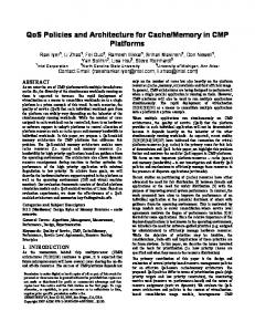
Application
Client
Client
Client
Memory Interface
RAM Block
RAM Block
RAM Block
Application
a) Private RAM blocks
Client
Client
Memory Interface
Scratchpad Interface
Platform Connector
Platform
Client
Scratchpad Controller
Scratchpad Interface
Scratchpad Interface
Request Ring Response Ring
Local Memory
b) Scratchpads with a ring interconnect
Figure 1: Transforming private RAM blocks to scratchpads. The memory interface between clients and storage is unchanged following the transformation. Only timing is different.
controllers. In order to share on-board RAM among multiple clients the memory must be partitioned and managed by a central controller. We call this service the scratchpad controller. The controller is responsible for partitioning a large memory into individual scratchpads, corresponding to private memories requested by clients. The controller then routes requests from scratchpads to their unique memory segments. This is implemented using an indirection table, mapping scratchpads to memory base offsets. Except for latency, moving storage to a different level in the memory hierarchy is invisible to software written for general purpose hardware. The change could range from missing in an L1 cache to suffering a page fault and swapping data in from a disk. While not an absolute requirement for FPGAbased scratchpads, having the ability to express memory I/O operations independent of their underlying implementation and latency is equally convenient on reconfigurable logic. In our implementation, the difference between a client using a private on-die RAM block and a scratchpad in a shared memory is only a single source line (see Section 2.7). The client using a RAM block invokes a module that instantiates on-die memory. To use a scratchpad instead, the client replaces this instantiation with a module that connects itself to the scratchpad controller. Each client requesting a scratchpad memory instantiates a scratchpad interface. This interface is private to a single client, transforming client-side references to requests in the
scratchpad controller. The scratchpad controller is a shared resource. Connecting multiple clients to the controller requires an interconnect and arbitration. For a small number of scratchpads, a set of point-to-point connections from scratchpad interfaces to the controller along with a round-robin arbiter works perfectly well. As the number of clients grows, the burden on FPGA routing becomes too great and a more sophisticated network is required. We have built a pair of token rings, using self-assembling rings described in [19]. The transformation from private RAM blocks to scratchpad memories is illustrated in Figure 1. Deadlocks are avoided by assigning requests to one ring and responses to the other. A pair of rings was chosen instead of a single ring with virtual request and response channels both to increase network bandwidth and because the FPGA overheads of channel buffering and multiplexing are similar to the simpler, multi-ring, solution. One ring stop is responsible for forwarding messages between the rings and the scratchpad controller.
2.2.1
Identifying scratchpads
The scratchpad controller must have a way of identifying individual scratchpads. Each scratchpad interface must be assigned a unique identifier that we call a scratchpad ID. Each instantiation of a scratchpad interface module takes a compiletime constant argument specifying a unique scratchpad ID. Every request from an interface module to the scratchpad controller is tagged with an ID. Reconfigurable logic and table sizes are minimized if the scratchpad ID space is dense. LEAP provides a namespace management tool for generating unique identifiers. This dictionary tool was originally conceived for mapping integer identifiers to strings in order to trigger printing of messages on a host from an FPGA without having to specify hardware logic for passing variable length strings. We have extended it to solve the general problem of managing identifier spaces, including syntax for managing numerically dense subspaces. Using LEAP dictionaries and conventions, an implementor allocating scratchpad IDs would specify: def VDEV.SCRATCH.FBUF_Y def VDEV.SCRATCH.FBUF_U def VDEV.SCRATCH.FBUF_V
"Frame buffer Y"; "Frame buffer U"; "Frame buffer V";
in order to allocate a group of scratchpads named FBUF Y, FBUF U and FBUF V. The dotted notation represents numerically dense subregions.
2.2.2
Initialization and addressing
An initialization step is required in order to subdivide onboard memory into individual scratchpads. At start-up, each scratchpad interface computes the size of its scratchpad array. The interfaces then send allocation requests to the scratchpad controller. The controller receives allocation requests and builds a partition table, mapping individual scratchpads to unique regions of memory. An error is signaled if the size of all allocation requests exceeds available memory. Each scratchpad interface operates in its own private, zero-based address space. Within the common controller, addresses are computed as the sum of the private address and a scratchpad’s on-board memory offset from the partition table. The mapping from private scratchpad array indices to on-board memory addresses is fully contained within the scratchpad controller. Although our current controller implementation maps all scratchpads dynamically at start-up and
2.3
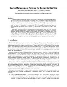
Client Client
Client
Marshaler
Marshaler
Marshaler
Private Cache
Private Cache
Private Cache
Scratchpad Interface
Scratchpad Interface
Scratchpad Interface
Client Memory Interface
Marshaling
Astute readers will have noticed a problem in our transformation of RAM block clients to scratchpad clients. Synthesis tools permit FPGA RAM allocation in any bit width. While the underlying hardware does not support arbitrary width, it is sufficiently flexible that memory is allocated relatively efficiently. In contrast, on-board memory is presented in chunks of words and lines, with some hardware adding write masks to support byte-sized writes. An easy, but unacceptably inefficient solution would be fixed mapping of RAM block addresses to word-sized onboard memory chunks. The fixed mapping would not support data widths larger than a memory word. It would also waste nearly the entire word for small data widths, turning a dense 1024 x 1-bit RAM block into a 64KB chunk, assuming a 64 bit word! To solve this mapping problem, the scratchpad interface interposes a marshaling layer between the client and requests to the platform interface. When objects are smaller than the memory word size, multiple objects are grouped into a single memory word. When objects are larger than the memory word size, the marshaling layer spreads objects across multiple words. In the first case the marshaler is forced to request readmodify-write operations in order to update an entry. In the second case the marshaler must emit multiple read or write requests in order to reference all memory words corresponding to a scratchpad location. From the client’s perspective, the word size remains the size originally requested. The LEAP platform provides a marshaling library module. Compile-time parameters declare the memory word size along with the desired scratchpad width and number of elements. The marshaler computes the dimensions of an on-boardmemory-sized container for holding the equivalent data and determines whether read-modify-write or group reads and writes are required. It also exports read and write methods that act on the requested array’s data type. The methods automatically trigger either read-modify-write or group reads and writes when needed.
2.4
Application
has no protocol for releasing regions, it would be relatively easy to extend the private protocol between scratchpad interfaces and the controller to permit dynamic release and reallocation of memory. Only the partition table must be updated. An ambitious implementation could even rebase region mappings in order to combine fragmented free memory blocks into larger chunks.
Private Caches
With the addition of marshaling we now have an architectural description for replacing RAM blocks with on-board memory scratchpads that is fully functional. Unfortunately, it will perform terribly. RAM block references that were formerly single cycle references and parallel for each block have been converted into a shared, high contention, higher latency resource. A cache is needed, both to provide lower latency and to reduce the number of requests that reach on-board memory. LEAP provides low latency, direct mapped, caches, though developers may specify their own cache implementations optimized for particular access patterns. The position of the cache, above or below the marshaler, is a compromise. Choosing to insert the cache between the client and the marshaler would eliminate many read-modify-write operations in the marshaler. However, read-modify-write
Platform Connector
Request Ring Response Ring
Figure 2: Client-facing model hierarchy, including marshaling from client data to on-board memory word-sized accesses, private L1 caching and a token ring networking scratchpad interfaces. The platform interface at the bottom of the stack forwards messages between the ring network and the scratchpad manager (not shown). operations are required because the data width above the marshaler is small. Consider a scratchpad of boolean values. Caching above the marshaler would require tag sizes to cover the address space but would have only one bit data buckets. This ratio of meta-data to actual cache data is unacceptable. In our implementation, both the private cache and the marshaler present the same interface to the client. The relative order of the marshaler and a cache is invisible to the scratchpad client. A compile-time heuristic could choose a locally optimal topology based on a scratchpad’s size and data type, placing the cache either above or below the marshaler. In our current implementation the cache is always inserted below the marshaler. The full hierarchy is shown in Figure 2.
2.5
Host Memory
The hierarchy has now expanded available FPGA-side memory from the capacity of on-die RAM blocks to the capacity of on-board RAM. This solution is fully functional on both stand-alone FPGAs and on FPGAs connected to a host computer. For scratchpad memories, on-die RAM block usage is reduced to fixed sized caches. Now we face the same question asked at the end of Section 2.1: What are we to do for algorithms with memory footprints too large for on-board RAM? If the FPGA is connected via a high speed bus to a host computer, the solution is the same as when we ran out of on-die memory: push the backing storage one level down in the hierarchy, using host memory as the home for scratchpad data. The method is essentially identical to the method for the on-board memory scratchpad controller in Section 2.2.2. An indirection table must map scratchpad memories to host
Client
Client
Memory Interface
Marshaler
Marshaler
Marshaler
Private Cache
Private Cache
Private Cache
Scratchpad Interface
Scratchpad Interface
Scratchpad Interface
Platform Connector
Central Cache Clients
Scratchpad Clients
Client
Client Fill / Spill
Request Ring
Client
Platform Host
Scratchpad Memory
Client
Marshaler
Marshaler
Private Cache
Private Cache
Central Cache Ifc
Central Cache Ifc
Platform Connector
Response Ring
Scratchpad Controller
...
Central Cache
Client Fill / Spill
Request Ring Response Ring
Local Memory
Figure 3: Full client-facing model hierarchy. Scratchpad clients (top-left) marshal requests to memory-sized chunks and are filtered by private caches. The scratchpad controller handles central cache spill and fill requests, transforming them into operations on the host scratchpad memory. Central cache clients (top-right) must provide their own spill and fill drivers, which likely connect to drivers on the host. The central cache protocol tags each request and cached line with a specific client, enabling proper routing of responses and spill or fill requests. addresses. Instead of reading and writing data from on-board memory, the scratchpad controller reads and writes host memory using either direct memory access or a protocol over an I/O channel.
2.6
Central Cache
Moving the backing storage from on-board RAM to host memory offers more space at the expense of access time. Configuring the now unused on-board RAM as a last-level cache can reduce this penalty. Because only one central cache controller is instantiated we can afford a more complicated controller. The platform’s central cache controller is set associative with LRU replacement. Clients connecting to the central cache identify themselves using a dictionary-based mechanism similar to the scratchpad ID allocation scheme described in Section 2.2.1. Like the scratchpad controller, the central cache constructs a unique address space for each client by concatenating client IDs and address requests from clients. This internal address space enables the central cache to associate entries with specific clients. Clients connecting to the central cache must provide functions for spilling and filling memory lines. Pushing the details of spills and fills out of the central cache allows a variety of clients to connect, all sharing the same on-board RAM, each with unique methods of reading and writing their backing storage. The LRU central cache policy automatically opti-
mizes the footprint of each client in the central cache based on the global access pattern of all clients. Figure 3 shows the full caching hierarchy. The scratchpad controller, shown at the left in the platform, is one client of the central cache. Misses from all L1 scratchpad clients are passed by the scratchpad controller to the central cache. The scratchpad controller provides spill and fill functions to the central cache that write and read lines from the scratchpad memory stored on the host. Other clients of the central cache are shown in the top right of the figure. In this example configuration, each client instantiates a private L1 cache and provides its own spill and fill methods that communicate with the host. While not currently implemented in the platform, the spill and fill methods could be extended with coherence messages. Along with coherence messages, the central cache tag structure could be enhanced to represent line ownership. Hybrid algorithms sharing data between the FPGA and the host could then communicate and force synchronization between FPGA-side caches and host memory.
2.7
Language
LEAP is written in Bluespec SystemVerilog [2]. While the platform framework is language independent, some Bluespec features simplified our implementation. The language offers powerful static elaboration and type algebra, enabling predicate functions that govern whether operations that invoke predicated methods will fire within an FPGA cycle. As long
as the user adopts a latency insensitive programming style, predicates defined within our implementation of scratchpad read request and response methods make it simple to replace a RAM block with a scratchpad by changing only a single line of source code. The method interfaces for RAM blocks and scratchpads are identical. Externally, they differ only in their timing and, consequently, their public methods’ predicates. All LEAP RAM block and scratchpad classes share the following interface: 1 2 3 4 5 6 7 8
interface MEMORY_IFC#(type t_ADDR, type t_DATA); method Action readReq(t_ADDR addr); method ActionValue#(t_DATA) readRsp(); method Action write(t_ADDR addr, t_DATA val); endinterface
The definition above declares the interface to the class MEMORY IFC. The class uses two abstract type names, t ADDR and t DATA, that will be bound to explicit types when instantiated. Three methods are defined: readReq requests a memory read, readRsp receives the read response and write updates the value at a location. Consider a trivial pipeline that reads a RAM block: 1 2 3 4 5 6 7 8 9 10 11 12 13 14 15 16 17 18 19 20
typedef Bit#(8) ADDR_T; typedef Bit#(4) DATA_T; // Allocate 256 4-bit elements MEMORY_IFC#(ADDR_T, DATA_T) mem