the TSI then produces a serial output out of these packets by permuting their respective time slots. TSIs are key devices in. Time-Division Multiplexing (TDM) ...
Load-balanced optical packet switching using two-stage time-slot interchangers A. Cassinelli (1), A. Goulet (1), M. Naruse (2), F. Kubota (2), M. Ishikawa (1) (1): University of Tokyo, Dept. Information Physics and Computing, 7-3-1 Hongo, Bunkyo-ku, 113-0033 Tokyo, Japan, Tel. +81-3-5841-6937 ; e-mail: {Alvaro_Cassinelli, Alain_Goulet, Masatoshi_Ishikawa}@ipc.i.u-tokyo.ac.jp (2): National Institute of Information and Communications Technology, 4-2-1 Nukui-kita, Koganei, 184-8795 Tokyo, Japan, Tel. +81-42-327-6209 ; e-mail : {naruse, kubota}@nict.go.jp
Abstract A photonic implementation of the load-balanced switch using feed-forward, two-stage optical time-slot interchangers is proposed here. Despite the simplicity of the architecture, preliminary simulations show a packet loss probability comparable to an architecture using FIFO buffers.
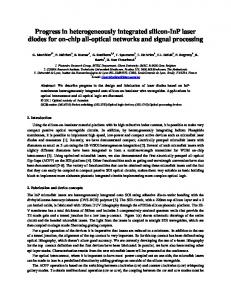
1- Load-balancing stage and TDM stage. A simple architecture to emulate a full-access TDM switch is the stage-controlled banyan network (SC-BN). It is a log2 N multistage interconnection network formed from 2×2 switches. All the N/2 switches within a stage are set either in the bar state or cross state; hence only log2 N control signals are necessary to operate the switch. It has been proven that the set of N permutations obtained from an SC-BN provides full access [5]. Owing to their simplicity, SC-BNs could be monolithically integrated using various photonic technologies such as electroabsorption (EA) modulators, semiconductor optical amplifiers and so forth. VOQ
1
…
N -1
1
…
L o a d -b a la n c in g s w itc h
0
…
0
…
II - Review of the load-balanced switch architecture The load-balanced switch architecture proposed by C.S. Chang et al. [4] consists of two switch stages and one buffer stage (see Fig. 1). The first switch performs load-balancing; it makes bursty traffic uniformly distributed at the input of the buffer stage. The buffer stage is composed of N independent buffers, each composed in turn of N separate FIFO queues known as Virtual Output Queues (VOQs) because packets are sorted and stored there depending on their output destination (packet destined to output j is stored in VOQ j). The second TDM switch services these queues by periodically connecting each to its corresponding output. The Load-Balancing and TDM stages are in fact alike. Both switching stages run through a periodic
III – Optical implementation of the load-balanced switch.
…
I - Introduction Packet switching in core and edge routers currently relies on electronic switching fabrics, which necessitates expensive optical-electrical-optical conversions. In addition, single-stage switch architectures with centralized scheduling are becoming increasingly impractical as the number of channels and the line rate become higher [1]. These reasons amply justify research on all-optical packet switches. A major drawback of photonics, however, is the lack of optical random access memories. Only simple optical buffers (OBs) using fiber delay lines (FDLs) are feasible at present [2]. The optical Time-Slot-Interchanger (TSI) is a well studied buffering [3]. The basic TSI design comprises a serial input fed by a stream of time-slotted packets; the TSI then produces a serial output out of these packets by permuting their respective time slots. TSIs are key devices in Time-Division Multiplexing (TDM) systems, since switching data among channels actually corresponds to permuting time slots between packets. A very promising packet switch architecture is the so called Load-Balanced Switch (LBS) [4]. It turns out that, internally, this architecture relies on a repetitive interconnection schedule: therefore, if implemented optically, it is likely that some part of the LBS can benefit being assembled out of optical TSIs. We present here a candidate architecture for an optical TSI which efficiently replace the standard FIFO buffers in the electronic version of the LBS. In order to minimize noise and switching losses, the TSI considered here does not contain any internal feed-back loop.
sequence of N particular interconnection patterns, Im (with m∈{0,…,N-1}) such that Im connects input i to output (i+m) modulo N. This permutation is set periodically in the LB or TDM stage at the time slots m+kN (where k is any integer). Conversely, at time slot t, input port i is connected to output port j with j=(i+t) mod N. Therefore, during a frame composed of N time slots, each input is connected once to each output (the switch is said to achieve full access). Because the loadbalancing stage equally distributes the traffic load among the inputs of the buffer stage, a deterministic TDM-like schedule that serves every virtual output queue to its corresponding output 1/Nth of the time gives a 100% throughput if the traffic is weakly mixed [4].
T D M s w itc h
N -1
Fig. 1. N input × N-output Load-balanced switch architecture. 2- Single-stage optical buffer In the case of the LBS architecture, a whole VOQ buffer with N FIFO queues, each of length b, can be emulated by a singlestage TSI that is able to delay packets from 0 to a maximum of bN-1 time slots. Indeed, because interconnection patterns repeat cyclically in the LBS, it is possible to forecast at which time slots an input will be connected to any output: a packet arriving at port r and time slot t will reach its destination d if it is delayed by exactly δ+kN time slots where δ=(d-r-t) mod N,
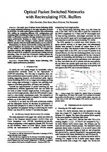
and k is any (positive) integer. As δ and N are unambiguously determined, only k (0≤k≤b-1) has to be chosen by the scheduling algorithm so as to avoid collision at the exit of the buffer (E1) with any packet scheduled in the previous Nb-1 time slots (see Fig. 3.a). If the current schedule is stored in a Nb long array E1[i] (0≤i≤Nb-1) where E1[i] indicates the state of occupation of the exit (E1) at time t+i, then the scheduling algorithm must find the smaller index k such that E1[δ+kN] is free (E1[Nb-1] is always free at the start of the scheduling cycle). At the end of each time slot, whether or not a packet was present at the input of the network, and whether or not it was possible to give it a schedule, the array is updated by shifting its content by one case, to account for the movement of packets in the fibers. Fig. 3a shows two possible implementations of the simple OB, functionally equivalent when packet schedules are computed so as to avoid collision, and therefore leading to the same probability of packet rejection. The second architecture needs roughly half of the square root of the total fiber length used in the first one, but a packet may go trough a larger number of potentially lossy fiber-combiners.
collision at E1. If there are several possible choices for k, then the smaller integer is preferred in order to minimize packet delay. If there is no such index, then the packet is considered lost. The obtained scheduling is optimal in terms of buffer occupancy and packet delay, and has an algorithmic complexity of O(b) -in the worst case, the search must consider only b pairs of memory cells. In practice, both stages can be fabricated from one-dimensional gate arrays, optical fibers, and passive splitter/combiners or wavelength-sensitive devices [2]. IV- Simulation One can realistically assume that after the Load Balancing stage, bursty traffic is changed into a Bernouilli process, every input of the buffer stage holding the same load. In the simulation, it was assumed that destination requests were also uniformly distributed. Simulations were carried out for a single and a double stage optical TSI, for N=16 input/outputs (a reasonable implementation goal). Figure 4 shows the probability of packet loss when varying parameter b (the equivalent length of a VOQ FIFO queue in the electronic version of the LBS). About 107 packets were generated per sample point in the graphs. As can be seen, performance of the double-stage architecture is only slightly degraded with respect to the single-stage delay-line buffer. This makes the proposed optical architecture an interesting substitute of the FIFO queues in an all-optical LBS.
Fig. 3. (a) Single and (b) double-stage loop-less optical TSI. 2- Double-stage optical buffer A single-stage TSI may appear impractical due to the large number of FDLs and/or switches required. The double-stage TSI shown in Fig. 3b is an alternative architecture needing only b+N switches instead of bN. It is composed of a first stage which provides delays multiple of the N time-slot-long cycle, followed by a sub-cycle delaying stage which provides an additional delay ranging from 0 to N-1 time slots. A packet requiring a total delay of ∆=δ+kN is delayed kN time slots in the first stage, then δ time slots in the second. The price to pay for reducing the number of switches/fibers is an additional source of contention at the exit of the first stage (E2), which is likely to reduce switch throughput. It is easy to extend the scheduling algorithm in the case of the double stage architecture: to avoid packet collision both at the exit of the whole switch (E1) and at the inter-stage crossing (E2), an additional array E2[j], 0≤j≤N(b-1), is maintained over time, representing the schedule of the exit of the first stage (E2[N(b-1)] is always free at the start of the scheduling cycle). To schedule a new packet, an index 0≤k≤b-1 must be found, such that E2[k.N] and E1[k.N+δ] are simultaneously free: this will mean that the packet is able to go, from first to second stage without collision at E2 (at time t+kN), and that it will find the requested permutation available (at time t+kN+δ), without
Fig. 4. Single-stage vs. double-stage buffer performance. V- Conclusions A photonic version of the load-balanced switch architecture using a stage-controlled Banyan network and a double-stage optical delay TSI was described. Despite an additional source of contention and the absence of any deflection or feed-back mechanisms in the buffer, overall performance remains comparable to the ideal single-stage TSI. Further study on generalized multi-stage architectures will be described at the conference. References 1. I. Keslassy et al., ACM SIGCOMM (2003), 189. 2. D.K. Hunter et al., J. Lightwave Technol., 26 (1998), 2081. 3. H.F. Jordan et al. IEEE Trans. On Comp. 43 (1994), 1309. 4. C.S. Chang et al., Comp. Commun., 25 (2002), 623. 5. A. Massini, Discrete Applied Math., 128 (2003), 43.