Localization and electron-electron interaction effects in magnetoresistance of p-type Ge/Ge1-xSix heterostructures Yu.G. Arapov1, G.I. Harus, V.N. Neverov, A.T. Lonchakov, N.G. Shelushinina and M.V. Yakunin Institute of Metal Physics, Ekaterinburg, 620219 Russia
1. Introduction The diffusive nature of electron motion in a disordered system results in quantum corrections to the Drude conductivity σ0 due to both the single particle weak localization (WL) effects and the disorder-modified electron-electron interaction (EEI) [1]. The WL and EEI parts of the total quantum correction ∆σ may be separated by a magnetic field B since the localization effect should be suppressed for B >> Btr = !c/2e"2 (" is the elastic free path) [2]. In contrast to the B sensitivity of ∆σ, for the EEI effect it is found that ∆σxy = 0 and ∆σxx = ∆σee (B = 0) at both ωcτ < 1 and ωcτ > 1 [3]. As a consequence, at B >> Btr the following expression for longitudinal resistivity takes place [3,4]: 2 ρ xx (B ) = ρ 0 + ρ 0 [1 − ( µB ) 2 ]∆σ ee (1) with ρ0 = 1/σ0. The interplay of classical cyclotron motion and EEI effect thus leads to the parabolic negative magnetoresistance (MR) [4,5]: ∆ρ / ρ 0 = −( µB ) 2 ∆σ ee / σ 0 .
(2)
1. Results and discussion
1
E-mail:
[email protected]
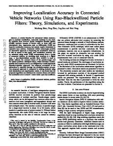
19
a) 1125a7
2
σ , e /h
18 17 16 15
b) 1124b 3
12 2
σ , e /h
We report on the results of the MR investigations for two samples 1124b3(1125a7) of strained multilayer p-type Ge/Ge1-xSix heterostructures with hole densities p = 2.5(2.8)·1011 cm-2 and mobilities µ = 1(1.7)·104 cm2/Vs at T ≥ 0.1 K in fields up to 2T. The logarithmic upturn of B = 0 resistivity takes place in both samples at T < 20 K (fig.1). For sample 1124b3, the negative MR is observed in the whole range of magnetic fields up to µB = 1 (B ≈ 1T) at T < 12 K (fig.2). The same situation takes place for sample 1125a7 at T < 1.3 K. But at T ≥ 1.3 K MR, also being negative for B < 10Btr ≈ 0.2 T, becomes positive for B ≥ 0.2 T (Fig.3). Estimation of the Fermi energy for complex Ge valence band in both samples yields EF ≈ ∆, where ∆ is the energy separation of the ground and the second hole subbands. Variation of internal uniaxial strain, as well as some differences in the Ge layer width, may result in variation of ∆ and thus in the degree of the second subband filling. We connect the observed positive MR just with the interplay of two types of holes due to the partial
11 0,1
1
T, K
10
Fig.1. Temperature dependencies of conductivity for samples 1125a7 and 1124b3
filling of the second subband. For two types of carriers with conductivities σ2 σ2) and give place to the positive one with increasing T (∆σee < σ2). Important is that for one or two types of carriers, as well as for negative or positive MR, extrapolation of the high-field (B >> Btr) ρxx(B2) dependence to B = 0 yields the same result:
ρ xx (B → 0) = ρ 0 (1 + ρ 0 ∆σ ee ) (4)
and makes it possible to estimate ∆σee and thus to separate WL and 2.2K EEI contributions to the total quantum correction at B = 0 (see figures 2,3). The result for both of 0,0 0,2 0,4 0,6 0,8 2 2 our structures is that ∆σee ≈ 2/3∆σ B ,T and ∆σWL ≈ 1/3∆σ. Fig.2. Resistivity ρxx against B2 for sample 1124b3. For p-type structures with strong Solid lines are the extrapolation of the B2 dependence spin-orbit coupling, positive weakto zero field. The inset shows the curve for T = 0.3K at localization MR is predicted for higher fields (ωcτ > 1). situation with EF ≈ ∆ due to a mixing 1,52 of the heavy- and light-hole states [6-8]. Contrary to this prediction, it 1125a is seen from figures 2 and 3 that MR 1,50 due to WL effect is negative at 1 B < 10Btr for both of our samples. 2 The disparity of our data with the 3 1,48 theory [8] may be due to the 4 different kind of impurity scattering 5 potential (remote impurities [9], but 1,46 not the short-range scatterers) or to the unconsidered role of the second hole subband, when the analysis of 1,44 data with due regard for a relation 0,0 0,2 0,4 0,6 0,8 1,0 between the times of phase breaking B ,T and intersubband transitions is Fig.3. Resistivity ρxx against B2 for sample 1125a7. needed [7,8]. T [K] = 1 - 1.55, 2 - 2.0, 3 - 2.5, 4 – 3.0, 5 – 4.2. But the main reason we believe is the strong uniaxial tension strain of Ge layers taking place in our heterostructures [10]. Due to uniaxial tension, a set of heavy-hole subbands is shifted to lower energies while a set of light-hole subbands is shifted to higher energies (if the hole energy is counted upwards) [11]. As a result, the interplay of the lowest different-type hole subbands becomes weaker and the degree of heavy-hole/light-hole mixing at the Fermi level diminishes. 2,10
ρxx, kΩ
7
2
2
3. Conclusions In summary, we analyze magnetoresistance data for p-type Ge/Ge1-xSix heterostructures with Fermi energy near the bottom of the second confinement hole subband (EF ≅ ∆). The negative MR due to a suppression of WL effect in the weak-field (B < Btr) region gives evidence that we are not in a situation with the strong spin-orbit scattering, in contrast with results of the theory [6,7]. Extrapolation of the B2 dependencies of the high-field MR (B >> Btr) to zero field is used to separate the WL and EEI parts of the total quantum correction to the conductivity. Acknowledgements The work is supported in part by Russian Foundation for Basic Researches, projects 01-0217685, 02-02-16401, 02-02-06864, 02-02-06168, INTAS YSF 01/1-156 and the 6-th concursexpertise RAS (1999) No. 68. References 1. B.L. Altshuler, A.G. Aronov in "Electron-Electron Interactions in Disorder Systems" (Amsterdam, North-Holland, 1985), p.1. 2. S. Hikami, A.I. Larkin, and Y. Nagaoka, Progr. Theor. Phys. 63, 707 (1980). 3. A. Hougton, J.R. Senna, and S.C. Ying, Phys. Rev. B 25, 6468 (1982). 4. K.K. Choi, D.C. Tsui, and S.C. Palmaateer, Phys. Rev. B 33, 8216 (1986). 5. Yu.G. Arapov, G.I. Harus, V.N. Neverov et al., Semiconductors 33, 978 (1999); Cond-mat/0203435. 6. N.S. Averkiev, L.F. Golub, G.E. Pikus, JETP 86, 780 (1998). 7. N.S. Averkiev, L.E. Golub, G.E. Pikus, Semiconductors 32, 1087 (1998). 8. N.S. Averkiev, L.E. Golub, S.A. Tarasenko, M. Willander, Phys. Rev. B 64, 045405 (2001). 9. Yu.G. Arapov, G.A. Alshanskii, G.I. Harus et al., Nanotechnology 13, 86 (2002); Cond-mat/0111229. 10. Yu.G. Arapov, G.I. Harus, N.A. Gorodilov, O.A. Kuznetsov, V.N. Neverov, L.K. Orlov, R.A. Rubtsova, A.L. Chernov, N.G. Shelushinina, Semiconductors 27, 642 (1993). 11. R.W. Martin, R.J. Warburton, R.J. Nicholas, G.J. Rees, S.K. Heywood, N.J. Mason, P.J. Walker, M. Emeny and L.K. Howard, Proc of XX ICPS. Thessaloniki, Greece, 1990, v.3, p.909; Phys. Rev. B 42, R9237 (1990).