Mar 10, 2006 - The developed field control module (FCM) of Spallation .... Automation software ... Lorentz force detuning effect on the basis of small-signal.
PHYSICAL REVIEW SPECIAL TOPICS - ACCELERATORS AND BEAMS 9, 032001 (2006)
Low-level rf control of Spallation Neutron Source: System and characterization Hengjie Ma, Mark Champion, Mark Crofford, Kay-Uwe Kasemir, Maurice Piller, Lawrence Doolittle, and Alex Ratti (Received 15 December 2005; published 10 March 2006) The low-level rf control system currently commissioned throughout the Spallation Neutron Source (SNS) LINAC evolved from three design iterations over 1 yr intensive research and development. Its digital hardware implementation is efficient, and has succeeded in achieving a minimum latency of less than 150 ns which is the key for accomplishing an all-digital feedback control for the full bandwidth. The control bandwidth is analyzed in frequency domain and characterized by testing its transient response. The hardware implementation also includes the provision of a time-shared input channel for a superior phase differential measurement between the cavity field and the reference. A companion cosimulation system for the digital hardware was developed to ensure a reliable long-term supportability. A large effort has also been made in the operation software development for the practical issues such as the process automations, cavity filling, beam loading compensation, and the cavity mechanical resonance suppression. DOI: 10.1103/PhysRevSTAB.9.032001
PACS numbers: 41.20.�q, 07.05.Dz, 02.30.Zz, 01.52.+r
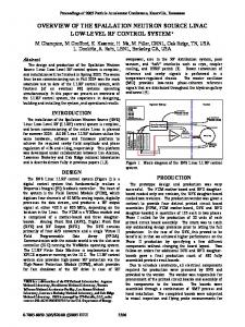
I. DIGITAL HARDWARE The developed field control module (FCM) of Spallation Neutron Source (SNS) LINAC Low-level rf (LLRF) control is in VXI format. It is all digital with 14-bit input and output resolution, and 40 MHz sampling rate. Excluding the peripheral ADCs and DAC, the entire FCM digital hardware is implemented on a single Xilinx field programmable gate array (FPGA) chip XC2V1500, including the direct digital synthesis (DDS) of the IF output. Figure 1 shows the mechanical construction of a FCM. All 96 commissioned LLRF systems are installed in 48 instrument racks distributed along the LINAC Klystron Gallery [1]. A. Development system The digital hardware of FCM is modeled in Verilog hardware description language (HDL). The framework and all the required functionalities [2] have been implemented. Currently the Verilog design has 24 components with over 3600 lines of code for synthesis, and over 3000 lines for simulation. The HDL development work by its nature is an ongoing process and the digital hardware will need to continuously evolve and be enhanced in order to adapt to the needs from the commissioning and operation. The ability of efficient and reliable support is equally important as the HDL design itself. For this reason, a great deal of effort was made also in creating a companion software system LLC-suite for providing an integrated development and cosimulation process as shown in Fig. 2. A large part of this process is automated. The process begins with 2300 lines of handwritten code for synthesis and 1300 lines for the test bench. In each run, the system subsequently machine generates additionally about 1000 lines of synthesis code for the standard functionalities in the design, including the top-level net list, and 2000 lines for the simulation models. The purpose of having an automated machine code generation and simulations is to minimize the risk of human errors. The test 1098-4402=06=9(3)=032001(12)
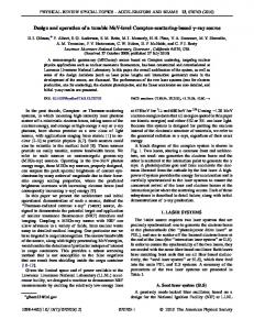
suite will continue to grow as more modeling is added into it. The detailed description of this development system, as well as a complete set of FPGA logic and software driver code, is available free at the LLC-suite website authored by Doolittle [3,4]. B. Current implementation Figure 3 shows the configuration of the implemented FCM hardware. It is a textbook series P-I controller [5] supported by a CORDIC phase rotator for frequency shifting, one set-point curve table, two feed forward data buffers, five additional data buffers for recording signal traces, and an rf timing sequencer. The key for a successful implementation of a digital feedback control has been the hardware latency. A careful HDL design for the P-I controller is able to let the signal go through the proportional control path in only 6 clock cycles, which is 150 ns for the 40 MHz sampling/system clock that the FCM has. Compared with the typical 1 � 2 �s total loop delay that SNS LINAC rf system has, the 6 clock cycle latency of the digital hardware has become insignificant, and that allows the use of an all-digital feedback control for the full bandwidth. Another unusual feature with this implementation is that it processes the I and Q signal data in its original sequential format throughout the entire process in a single channel, resulting in minimal hardware and minimum latency. The implemented essential functionalities also include four history data buffers for simultaneously recording four vector signal traces selectable from the forward and reflected wave of the rf power, cavity field, and LLRF output drive, plus an extra data buffer for study. The history buffers have the standard ZOOM/PAN feature of a digital storage oscilloscope (DSO) for variable time resolutions and starting points. The DSO feature proved essential for the system development, troubleshooting, and operation automation. There are two switched 8-kByte feed forward
032001-1
© 2006 The American Physical Society
HENGJIE MA et al.
Phys. Rev. ST Accel. Beams 9, 032001 (2006)
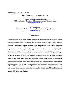
FIG. 1. (Color) FCM of SNS LINAC LLRF is built with a VXI carrier and three daughter-cards: analog front end in the left, digital front end (DFE) in the middle and rf output in the right. The core of this unit is DFE which performs all the control functions.
data buffers, one for the rf drive waveform of cavity filling, and another for the beam loading compensation. There is also a 1-kByte long table for the set-point curve. A CORDIC algorithm based phasor rotator is also coded in the HDL [6]. The rotator spins the set-point phasor to shift
the output frequency up to �= � 645 kHz. The function of the output frequency shift is needed during the cavity tuning or heating. The phase reference signal data is collected in a time slot either prior to or after the rf pulse. That allows the reference signal to come into the system either
Verilog Modeling: NO
O
K
?
Functionalities
Machine Code gen.: Netlists
RTL Compilation Iverilog / ModeSim
YES
Verification Test Lab.
GUI/Control Automation software development
Machine Code Gen. : drivers
PAR Xilinx ISE
Synthesis XST / Synplify NO
OK
YES
?
End-to-End System Behavioral Simulation
FIG. 2. (Color) Verilog HDL modeling and cosimulation process for the development of FCM digital hardware.
032001-2
LOW-LEVEL RF CONTROL OF SPALLATION NEUTRON . . .
Phys. Rev. ST Accel. Beams 9, 032001 (2006)
FPGA: X2V1500 SP_Vec_Rot
DIFF
Phase_Rot
FIR
+ G(z)
width := 16 size := 1024 ts := 25ns
-
Kp
Gain_Ramp
error
s1
SP_Sel
INTEGRAL
err_trip
I
SP_Table width := 16
s z
FLD_BUF
adc_CAV MUX
adc_FWD
RFL_BUF
s z
s z
adc_REF
RF TIMING CNTRL
DIAG_BUF
adc_RFL mux5x5
probe
Ki IF_BOOST clk80
rf_gate ff_start fb_start trip_del ramp_stp
s2 PROTECTION hpm mps err_trip
FF_table_2
OUT_BUF size := 1024
size := 8192
CAVITY
comb2_s1
FF_table_1
TIMING_SEQ
FWD_BUF
s z
s3
a b c d
AGAIN
DCPL
Gain
SW
InterLock Logic
Loop_Latency S
z
Delay
drive
kc := 1kHz
fwd
k := A
rfl
dac_z2s1
td := 0.000001
FIG. 3. (Color) A model of SNS rf control system. All required control functionalities in the blue box are implemented in one FPGA chip.
through a dedicated channel or through the channel timeshared with the cavity signal [7]. After the place-and-route, the entire design has used about 20% of the logic slices, 30% of the RAMBs, 50% of the IOBs, and 8% of the multipliers of the XC2V1500 FPGA chip. II. SYSTEM CHARACTERIZATION A. Frequency response A system analysis at the cavity probe where the end-toend point in the control loop is defined can be conveniently carried out in continuous time. The CPI 805 MHz klystron used in the SNS LINAC exhibits a fairly good linearity around the normal operating point. If we can ignore the Lorentz force detuning effect on the basis of small-signal analysis, we may assume a simplistic 1st-order model for the cavity which is perfectly on its resonance [8]. Under these assumptions, we may first examine the theoretical limits posed by the loop delay on the loop gain and consequently on the control bandwidth through a linear timeinvariant (LTI) system analysis. The open-loop transfer function is expressed in (1) as � � !bpf K !b G�s� � Kp � g � 1 � i � � � e���s s s � !b s � !bpf � g � Kp � !b �
�s � Ki � ���s �e ; when !b !bpf s�s � !b � (1)
where !b and !bpf are the half-bandwidth of the cavity
and the output bandpass filter of the LLRF. The � is the total loop delay. Kp is the digital proportional gain produced inside the P-I controller, while g is the lumped-sum gain along the analog path of the feedback loop outside of the controller. Therefore, the product g � Kp represents the total loop gain. The scalar Ki is the integral gain. The effect of the Klystron bandwidth is not included in the transfer function as the klystron bandwidth is as wide as 3 MHz, and has an insignificant effect for the bandwidth of analysis. The above open-loop transfer function indicates a Type 1, and minimum �n � 2�th-order system, where the number n is the order of the Pade´ approximation for the delay term. For a unity feedback, the closed-loop transfer function therefore is G�s� 1 � G�s� g � Kp � !b �s � Ki � � e���s � : (2) s�s � !b � � g � Kp � !b �s � Ki� � e���s
GB�s� �
The added poles from the loop delay � have created the possibility for instability to occur, and limited the maximum loop gain that can be used, and that in turn has limited the control bandwidth and precision. To analytically examine the stability of such a system, we may first simplify the closed-loop transfer function (2) by setting Ki � !b to cancel the cavity pole, and substitute the delay term with a 3rd order Pade´ approximation. That renders a characteristic function
032001-3
HENGJIE MA et al.
Phys. Rev. ST Accel. Beams 9, 032001 (2006)
� � � 1 3 F�s� � s 1 � � � s � g � Kp � !b � 1 � � � s 4 4 � 1 1 � �� � s�2 � �� � s�3 : 4 24
(3)
Using Routh-Hurwitz criterion, we obtain a condition for the system stability approximately as g � Kp �
1.0
0.25 dB
1 dB
-1 dB
15 3 dB
10
-3 dB 6 dB
5
60 deg
0
-6 dB
-5
-10
8dB
3dB BW = 95 kHz
-12 dB
-15 Stop frequency = 115kHz
-225
-180 -135 -90 -45 Open-Loop Transfer Function Phase (deg)
-20 dB
0
FIG. 4. (Color) Graphical analysis with Nichols chart for the performance and stability of SNS rf control system. A worst case of 2 � sec loop delay is assumed.
032001-4
LOW-LEVEL RF CONTROL OF SPALLATION NEUTRON . . . bandwidth, but not the control error as it becomes zero after the system reaches a steady state. Contrary to the NC cavities, the superconducting cavities have the time constants comparable to the rf pulse width. The control system cannot reach a steady state within the duration of the rf pulse. In a transient state, the amount of loop gain affects not only the control bandwidth in the form of responding time, but also the control error. The Nichols chart analysis indicates that in the case of SNS SC cavities, the maximum loop gain that can be used without causing instability is 210, while the optimal value is about 75. Based on control theories, with only the feedback control and the gain of 75, the estimated maximum field error would be about 1.3% in the case of 100% beam loading, which exceeds the specified precision of 0.5%. Because of that, the help of a feed forward compensation is necessary for achieving the required control precision for SC cavities. B. Transient response On the commissioned NC cavities, the transient response was measured with a commonly used method for a P-I controller. A test step is added to the amplitude set point, and the response at the cavity field probe is observed. The choice of end-to-end point is consistent with the one used in the previous section. The size of the step was 12.5% of the nominal field level. The systems were tuned up by matching the time constant of the controller integrator to that of the cavity for a zero-pole cancellation. Figure 5 shows the test result on drift tube linac (DTL) Tank 1 with a
Phys. Rev. ST Accel. Beams 9, 032001 (2006)
cavity bandwidth of 16 kHz. The result shows the control system reaches to a critically dampened condition when the loop gain is at about 10, and the corresponding closedloop control bandwidth in baseband is about 166 kHz. This result is close to the predicted value. Figures 6 and 7 show the transient response tested on a superconducting cavity system SCL-12a. The test method used on SC cavities was slightly different from that for NC cavities. The 50 �s rectangular pulse was injected into the loop from the feed forward signal input, and the response was observed at the cavity rf input port. The choice of endto-end point is different, but the test is equivalent, and so the test results for the two types of cavities can be comparable. The pulse amplitude is 20% of the normal rf drive level. The high-beta SC cavity SCL-12a has a halfbandwidth of 560 Hz, and operates at a field gradient of 9 MV=m. A maximum loop gain of 99 was measured for the system to reach a slightly under damping ratio of 0.78, and achieved 3-dB control bandwidth is about 56 kHz. The measured value of the control bandwidth is lower than the 95 kHz predicted in the Nichols chart. The transient response to a 10 mA, 300 �s unchopped beam pulse was also observed on the high-beta superconducting cavity SCL-12a as shown in Figs. 8 and 9. The test beam pulse had an about 10 �s rise time on its leading edge. With a high loop gain of 89 and without any feed forward compensation, the beam loading produced an initial peak error under 0.3% on the cavity field amplitude, and the error then reduced to less than 0.1% after about 30 �s.
1800
Changes of cavity field and RF drive amplitude (ADC counts)
←← Dead time (delay from DAC to ADC) = 1.0365 usec. 1600
1400 Control bandwidth ωb = 165.2581 kHz @ ξ=0.707 Total Loop Gain: 9.9207 for ξ=0.707 Settling time (95%): 4.2814µs Cavity pole Kc: 16.6579 kHz
1200
1000
800
600
400 System ID: DTLLLRF:FCM1:
200
−200
Cavity field, ξ=0.707 LLRF drive, ξ=0.707 Cavity field, ξ