Semiconductors, Vol. 36, No. 8, 2002, pp. 883–888. Translated from Fizika i Tekhnika Poluprovodnikov, Vol. 36, No. 8, 2002, pp. 947–952. Original Russian Text Copyright © 2002 by Vintsents, Zaitsev, Zoteev, Plotnikov, Rodionov, Chervyakov.
SEMICONDUCTOR STRUCTURES, INTERFACES, AND SURFACES
Low-Threshold Defect Formation and Modification of Ge Surface Layer under Elastic and Elastoplastic Pulsed Laser Effects S. V. Vintsents*, V. B. Zaitsev**, A. V. Zoteev**, G. S. Plotnikov**, A. I. Rodionov**, and A. V. Chervyakov** * Institute of Radio Engineering and Electronics, Russian Academy of Sciences (Fryazino Branch), pl. Vvedenskogo 1, Fryazino, Moscow oblast, 141120 Russia e-mail:
[email protected] ** Faculty of Physics, Moscow State University, Vorob’evy gory, Moscow, 119899 Russia Submitted July 23, 2001; accepted for publication November 28, 2001
Abstract—Changes in the spectra of fluorescence of dye (rhodamine B) molecules adsorbed on a Ge surface and modification of the parameters of Raman and diffuse scattering of light by a semiconductor surface subjected to elastic and elastoplastic effects of pulsed laser radiation are studied. Using contactless photoacoustic measurements based on the laser beam deflection technique, the amplitude of the threshold surface strain is estimated at ~5 × 10⁻⁵. An appreciable quenching of the fluorescence of the adsorbed probe molecules, an abrupt broadening of the molecular spectra, and an above-threshold increase in the intensity of the diffusively scattered light are observed upon the transition to the range of energy densities corresponding to the inelastic strain formation. The larger the laser-induced strain, the smaller the frequency and the width of the Raman lines, and the higher their intensities. The physical nature of these effects is discussed. © 2002 MAIK “Nauka/Interperiodica”.
INTRODUCTION Previously, the final stages of the controllable damage of semiconductors and metals exposed to multiple laser pulses were observed at relatively low threshold energy densities W0 ⱗ 0.1 J/cm2 [1–4], which, in the conditions of local (Gaussian beam radius ω ≈ 10–100 µm) short-term heat release, are characterized by the socalled size effect: W0 ∝ ω [2, 5–8]. Most of the experiments were based on the techniques that are sensitive only to the macrodamage of semiconductors (see, e. g., [2, 3] and the references therein). It was not until recently that the initial stages of microscopic changes, whose accumulation within small regions (10–100 µm) may cause macrodamage, have received the attention they deserve [9–11]. It has been shown already that, under the local effect of a relatively small number of laser pulses (N ⱗ 103), the thermal stress produced in the surface layer of a semiconductor results in plastic microstrains, which cause (at the energy density W ≈ W0) a significant threshold change in the parameters of the insulator slow states (ISS) localized in the oxide layer on the germanium surface [10]. However, in the conditions specified, the microscopic defect formation in the oxide film is not the only result of the photoinduced deformation; a considerable change in the microstructure of the semiconductor surface layer, a radical restructuring of the deeper layers [7, 8, 10], and the formation of superstructures on the surface [3, 12] are also possible.
For a complex investigation of the early stages of microplastic changes produced near the actual (i.e., covered with a thin oxide film) germanium surface, we combined several optical nondestructive techniques; namely, molecular luminescence probing, diffuse and Raman scattering, and photothermal deformation of the surface were used. EXPERIMENTAL Similar to [10], we studied the (111) surfaces of high-resistivity (resistivity ρ = 25–30 Ω cm) n-Ge single crystals doped with Sb and etched in H2O2 at room temperature. After the etching, the germanium samples were kept in air for more than a day, during which a 20to 30-Å-thick GeO2 layer of hexagonal structure was formed on the Ge surface. Then, the “real” surfaces thus obtained were subjected to pulsed laser radiation in air. A laser beam of micrometer size, similar to that described in [10], was used in the scanning mode; for the experimental techniques implying nonlocal action, five-to-six regions of ~3 × 5 mm2 area were formed by scanning the sample surface (we used the samples of size 20 × 5 × 0.3 mm3). Each of the regions was characterized by its specific energy density W of the laser radiation with λ = 0.53 µm, the Gaussian spot of the size 2ω ≈ 70 µm, the pulse duration τ0 ⲏ 350 ns, and the number of pulses N ⱗ 103. The range of W variation was chosen between 10 and 250 mJ/cm2, which is much
1063-7826/02/3608-0883$22.00 © 2002 MAIK “Nauka/Interperiodica”
VINTSENTS et al.
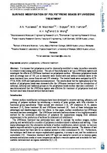
884 10 6 dUz /dr 12
~0.8 nm and a spatial resolution along a sample of ~10 µm. As the position-sensitive device, we used a microchannel plate and a CCD array for detecting the fluorescence spectra and for studying the Rayleigh scattering, respectively. A halogen lamp (1000 W) with an interference filter adjusted to 530 nm excited the fluorescence of the probe molecules.
(a)
2 8
Probe molecules were those of rhodamine B deposited on the semiconductor surface from an alcoholic solution. The surface concentration of the dye molecules amounted to 2 × 1013 cm–2, which corresponds to a ~0.2 monolayer according to the data obtained using a piezo-resonance balance. Special experiments indicated that neither the adsorption of the dye at the surface nor the radiation with intensities used in the experiments changed the degree of homogeneity of the surface or the spectrum of surface electron states (SES).
1 3
4
4 5
Uz , Å 4
3
2
Additional study of Raman and diffuse scattering spectra of the probing light was carried out using a DFS-52 spectrograph for the germanium samples excited by an argon laser with λ = 0.488 µm. The resolution of the Raman scattering (RS) spectral measurements was improved by using p polarization of the laser beam incident upon the sample surface at the Brewster angle with an intensity of ~0.5 W/cm2.
(b)
2
Instantaneous spatial profiles of the quasi-static strains on the germanium surface dUz/dr = f (r) and the effective normal elastic displacements Uz(r) were detected using an advanced method of photothermal surface strain (PTSS) in accordance with the technique employed in [14, 15].
3 1 4
1
RESULTS AND DISCUSSION
5
The results will be outlined by proceeding mainly from the lower to higher densities of laser pulse energy W. 0
40
80 r, µm
Fig. 1. Kinetics of the spatial profiles of (a) quasi-static strains dUz/dr = f (r) and (b) the effective normal displacements Uz (r) of the actual Ge surfaces at the elastic stage of the focused laser-beam effect W ≈ 8–10 mJ/cm2 Ⰶ W0. The profiles were measured at the time t counted from the beginning of the laser pulses, which recurred within intervals ∆t ≈ 100 µs and featured the following coordinate r and time t dependence of the intensity [15]: I(r, t ) = 2
Wexp(–r2/ω2)(t/ τ 0 )exp(–t/τ0) with the characteristic time constant τ0 ≥ 350 ns. t = (1) 1, (2) 2, (3) 6, (4) 10, and (5) 18 µs.
lower than the melting threshold Wm ⲏ 1.2 J/cm2 [13] calculated at τ0 ⲏ 350 ns [13]. The fluorescence spectra were measured using a hyperspectrometer, which is a system with a positionsensitive sensor and ensures a wavelength resolution of
The profiles of dUz/dr = f (r) and Uz(r) obtained in germanium in situ under the nondestructive (elastic) pulsed laser effect at W ≈ 8–10 mJ/cm2 Ⰶ W0 are plotted in Fig. 1. The profiles have the shape of a hump appearing at the semiconductor surface and turned out to be similar to those previously obtained for metals [14, 15]. The kinetics of the displacement profiles makes it clear that the intervals between laser pulses (∆t ≈ 100 µs) is sufficient for the sample surface to cool entirely and return to its unperturbed (unstrained) “horizontal” state. When W increased to W0 ⲏ 70 mJ/cm2, the displacement profiles retained their smooth shape and no small-size (on the order of micrometers) spatial fluctuations Uz appeared. As in [2], the profiles at W0 corresponded to the largest (along the beam radius r and for the time t) shear strain ϕ0 ≡ (dUz/dr)max ≈ 5 × 10⁻⁵ (Fig. 2, curve 1). Note that the drop in the photostrain signal at the thresholds W0 is mostly caused by the development of the final stages of damage in germanium (at N ≥ 106) accompanied by an abrupt decrease in the fraction of mirror-reflected light [2]. SEMICONDUCTORS
Vol. 36
No. 8
2002
LOW-THRESHOLD DEFECT FORMATION AND MODIFICATION OF Ge SURFACE LAYER
The results of studying the fluorescence of the dye on the germanium surface are shown in Fig. 3. It is clearly seen that, at small W (W < W0), both the intensity (IPL) and the half-width of the rhodamine B spectral line (λ1/2) are nearly constant. This corresponds with the data previously obtained from electrical measurements of the slow states in an insulator [10], which suggest that no dramatic changes are produced under the thermoelastic local laser effect either in the germanium layer (Ge) or in the oxide film (GeO2). We observed only a slight quenching of the fluorescence from the adsorbed rhodamine B molecules (at W ≈ 50–70 mJ/cm2), which was attributed to the prethreshold laser-induced generation of a small number of deep slow states in the oxide layer [10]. Such states may apparently arise from the elastic bending flexure of the thin insulator films during the multiple photostimulated expansion of the surfacelayer bulk with the vertical displacement amplitude Uz ≈ 1–10 nm [2, 8]. As is known [16], the deep traps in an insulator can act as acceptors of the electron excitation energy transferred from the probe molecules, thus, promoting moderate quenching of the molecular fluorescence observed at W < W0. The most abrupt changes in the rhodamine B molecular spectra of fluorescence are observed at W ≈ 70–85 mJ/cm2, i. e., at the thresholds W0 [10]. These changes comprise an appreciable (from five to ten times) quenching of the fluorescence intensity (Fig. 3, curve 1) and a simultaneous broadening of the fluorescence spectra of the probe molecules (Fig. 3, curve 2). Let us emphasize that, at W ≈ W0, no shift of the fluorescence peak (λmax) was noticed at the threshold. In our opinion, this may be explained by the fact that the irreversible plastic strain induced at the energy densities in the vicinity of W0 (Fig. 2) results in the additional electronic states in the damaged oxide layer on the germanium surface. Along with an increase in the concentration of the deep electron traps (the ISS), we observed a pronounced increase in the concentration of shallow fluctuation states in GeO2 in the vicinity of the allowed band edges. The latter circumstance is indicated by an abrupt drop in the ISS charging threshold upon the photoinjection of charge carriers from Ge [10]. Similar to the deep traps in insulators [16], the fluctuation states in GeO2 are likely to be effective acceptors of the probe-molecule photoexcitation energy that is nonradiatively transferred into the solid medium. In fact, the critical radius of the energy transfer by the Forster–Dexter mechanism in such structures equals ~5 nm, and the most intense generation of the fluctuation states is in the oxide region (with a thickness ⱗ3–5 nm) that is directly adjacent to the germanium interface; this region is the most disordered [17]. It should be noted that the local electric fields that appear upon the recharging of such defects could produce only a slight effect on the position of the fluorescence peak λmax of the probe molecules, because the Coulomb charged centers affect only the molecules which are located in their vicinity, i.e., within 1 nm [18]. SEMICONDUCTORS
Vol. 36
No. 8
2002
885
0 Isc /Isc
10 5 (dUz /dr)max 6 5
2.5 1
4 2.0 3 2 1.5
2 1
1.0 0
W0 0
50
100 150 W, mJ/cm 2
200
250
Fig. 2. (1) The increase in the largest (along the radius r and for the time t) elastic strain (dUz/dr)max with increasing W and the drop of the PTSS [2] signal at the thresholds W0 (1); (2) W-dependence of the intensity of light diffusely scat0
0
tered from the Ge surface Isc/ I sc , where I sc is the intensity of light scattered from an unirradiated surface (W = 0).
The considerable (from 1.5 to 2 times) broadening exhibited by the fluorescence spectra of probe molecules at the thresholds W0, i. e., upon the transition from the elastic to the elastoplastic straining of the semiconductor, may be attributed to the pronounced growth of the geometric heterogeneity of the surface, which presents direct evidence of the initiated irreversible (residual) displacements ∆Uz of the real germanium surface. The amplitude of these displacements is apparently close (within an order of magnitude) to the amplitude of the maximal reversible elastic displacements of the germanium surfaces Uz max ~ 1–10 nm, which were previously studied by the PTSS method [2, 8]. Note that, at the thresholds W0, the value Uz max is comparable to the mean radius of the induction-resonant Forster–Dexter transfer of the electron excitation energy r0 ≈ 5–6 nm [16] and the inhomogeneous broadening of spectra is maximal; therefore, the molecular probe technique turned out to be especially effective in this case. A distinct increase in the intensity of the diffuse scattering was observed at W ⲏ 85–100 mJ/cm2 and tended to level off at higher energy densities (Fig. 2, curve 2). In contrast to the short-range testing of the surface by the luminescent molecular probes, the scattered light allows one to probe the germanium surface to a depth that is essentially larger than r0 and can be as large as R0 ~ 100 nm for the excitation wavelength λ
VINTSENTS et al.
886
λ1/2, nm
0 IPL /IPL 1.0
80 1
{δν, δν1/2} 0 –1
0.8 70 0.6
–2
2
1
–3 2
0.4
60
W0 –4 Raman intensity, arb. units 2.0
0.2 50 0
W0 0
40
80 120 160 200 240 W, mJ/cm 2
3
1.5
W0
1.0 0
Fig. 3. (1) Threshold quenching of rhodamine B molecular fluorescence and (2) threshold broadening of the fluorescence spectra of the probe molecules on the actual germanium surface that was preliminarily subjected to elastic (W < W0) or elastoplastic (W > W0) strains as a result of 0
pulsed laser irradiation. I PL is the fluorescence intensity of an unirradiated sample.
used in the experiment. In these conditions, the enhancement of the diffuse scattering observed at W ⲏ (1.2–1.5)W0 most likely reflects the kinetics of the gradual accumulation of the microplastic changes, when the scattering inhomogeneities induced in the surface layer grow with W and become comparable in size with R0 or λ. We believe that, at the initial stages of the microplastic changes (i. e., in the vicinity of W0), the inhomogeneities grow mainly due to pulse-to-pulse accumulation and the subsequent diffusion of point rather than extended defects [3]. This is because the local laser irradiation with an energy density near the threshold W0 induces the thermal stresses σ0 ≈ 2–3 MN/m2 [2, 8], which are far below the minimal stresses that give rise to the heterogeneous nucleation and motion of dislocations at room temperature and the related dislocationrelated plasticity of germanium σ > 20–200 MN/m2, as determined from the experiments with contact loading of germanium [19]. In fact, in our experimental conditions, the local laser-induced heating does not exceed ∆T ⱗ 100°C [2, 8] at the thresholds W0, while the brittle point in germanium is T ≈ 500°C. In accordance with the well-known classification of the microplasticity phenomena ([19], p. 243), in the range of a relatively low photoinduced stress, which is the case, the hetero-
40
80
120 160 W, mJ/cm 2
Fig. 4. Changes in the parameter of Raman scattering from actual germanium surfaces subjected to preliminary pulsed laser irradiation versus the energy density at the center of the laser spot W: (1) Raman line frequency shift δv, (2) narrowing of the linewidth δv1/2, and (3) an increase in the intensity of Raman scattering.
geneous–dislocation mechanism of microplastic strain gives way to a defect–diffusion mechanism: both the initial nucleation of the plastic microstrains (dislocation loops) and their further growth are entirely governed by the diffusion processes in the field of the point defects. The significant role of the kinetics of defects in the observed microplastic processes is also indicated by the somewhat unexpected behavior of the Raman spectra. As W grows, the RS line (~301 cm–1) shifts to lower frequencies by δv, which is usually observed during amorphization, when the degree of crystallinity decreases and microcrystals appear in the material [20] (Fig. 4, curve 1). Along with this, the full width of the RS line at half maximum decreases with W by δν1/2 (Fig. 4, curve 2), which is typical of a growing degree of order. It should be emphasized that the aforementioned changes in the RS spectra of the germanium samples were observed in both the elastic (W < W0) and the elastoplastic (W > W0) modes of the multiple (N ⱗ 103) laser-induced straining and did not feature a pronounced threshold character (Fig. 4). The RS spectrum narrowing observed in the entire W range may be caused by the existence of an initial (at W = 0) inhomogeneous broadening of the RS spectra in the studied samples due to the overlapping of local SEMICONDUCTORS
Vol. 36
No. 8
2002
LOW-THRESHOLD DEFECT FORMATION AND MODIFICATION OF Ge SURFACE LAYER
stress fields that exist in the vicinity of various growthrelated microinclusions and extended defects, e. g., dislocations. Is it well known that such local fields of compression and tension of the crystal lattice in the vicinity of defects give rise to a considerable broadening of the RS spectra [21]. In fact, the initial RS linewidth for unirradiated samples was v1/2 ≈ 7.5 cm–1, whereas the RS line of the reference germanium single crystal with a low concentration of growth dislocations had a width of ~ 5.5 cm–1. In the conditions of multiple laser irradiation realized in our experiment (in both the elastic and elastoplastic modes), an increase in W resulted in the increase of the concentration of “frozen” vacancies (“vacancy pump” model [19, 22]), whose migration to dislocations or other sinks may effectively reduce the fluctuations of microstresses existing before exposure in the vicinity of defects. To illustrate such a positive influence of defects, we may recall the well-known relaxation of microstresses in the elastic model of interstitial precipitate, where the discrepancy in the size of an inclusion and semiconductor void (for example, the inclusion is larger than the void) is significantly reduced because the “excess” material of the host is removed in the course of the diffusive absorption (emission) of point defects: vacancies, interstitial atoms, etc. ([19], p. 203). Another argument in favor of the noticeable contribution of vacancies (and other point defects) to the observed defect–diffusion microplasticity [19] is presented by an increase in the intensity of RS (Fig. 4, curve 3). According to the theory of RS for an anharmonic crystal containing vacancies [23], the presence of vacancies should produce an additional polarization of the lattice around the point defect, thus making additional contributions to the dipole moment and renormalizing the spectral width and position of both the fundamental and combination absorption lines. Usually, the defects make only a moderate contribution to these parameters; however, the laser-induced cyclic thermal strains may cause a considerable accumulation of defects (vacancies) [3], which can contribute significantly to both the frequency shifts and the increase in the intensities of the Raman scattering and the fundamental absorption [23]. It should also be noted that, when the concentration of the point defects is high, various types of instabilities might develop and give rise to the formation of a microcrystalline superstructure, which is possibly the case in our experimental conditions [3, 12]. In order to verify the latter statement, one has to perform a direct study of the changes induced in the micromorphology of the surface by the elastoplastic laser effect. This may be done using scanning atomic-force microscopy, which we are planning to perform. CONCLUSION (1) We studied the changes in the fluorescence spectra of dye (rhodamine B) molecules adsorbed on a gerSEMICONDUCTORS
Vol. 36
No. 8
2002
887
manium surface and in the parameters of the Raman and diffuse scattering of light, which were the result of elastic (W < W0) and elastoplastic (W > W0) pulsed laser effects with a threshold strain amplitude of ~5 × 10⁻⁵ [2]. (2) Along with the deep traps in the insulator (GeO2), the slow fluctuation states appearing in the oxide layer at the thresholds W0 ≈ 70 mJ/cm2 [10] effectively absorb the electron photoexcitation energy from the adsorbed probe molecules and cause a pronounced quenching of their fluorescence at W ≥ W0. The energy transfer to the fluctuation states near the insulator/semiconductor interface is accompanied by a threshold (with respect to W) broadening of the fluorescence spectra of the dye, which suggests a steep rise in the geometric heterogeneity of the germanium surface due to irreversible (residual) surface displacements ∆Uz ~ 1–10 nm that arise at the thresholds W0. (3) The observed behavior of the Raman and the diffuse scattering parameters indicates that a gradual accumulation of microplastic changes occurs in the surface layer of the semiconductor (Ge). The initial stage of modifications includes primarily the generation, the accumulation (from pulse to pulse), and the diffusion to sinks of the point defects (presumably, vacancies), which, at W ≥ (1.2–1.5)W0, (i) lead to the growth of scattering irregularities thus enhancing the intensity of the diffuse scattering and (ii) effectively reduce the inhomogeneous broadening of the RS spectra caused by local microstress fields. (4) High concentrations of point defects in germanium are attainable in the elastoplastic mode of multiple local laser effects; therefore, irradiation in this mode may cause an instability in the point defect field with the subsequent formation of periodic surface superstructures. REFERENCES 1. P. M. Fauchet, Phys. Lett. A 93, 155 (1983). 2. A. G. Barskov and S. V. Vintsents, Fiz. Tverd. Tela (St. Petersburg) 36 (9), 2590 (1994) [Phys. Solid State 36, 1411 (1994)]. 3. B. L. Volodin, V. I. Emel’yanov, and Yu. G. Shlykov, Kvantovaya Élektron. (Moscow) 20 (1), 57 (1993). 4. C. S. Lee, N. Koumvakalis, and M. Bass, Appl. Phys. Lett. 47, 625 (1982); Opt. Eng. 22, 419 (1983). 5. C. S. Lee, N. Koumvakalis, and M. Bass, J. Appl. Phys. 54, 5727 (1983). 6. S. S. Cohen, J. B. Bernstein, and P. W. Wyatt, J. Appl. Phys. 71, 630 (1992). 7. S. V. Vintsents and S. G. Dmitriev, Pis’ma Zh. Tekh. Fiz. 21 (19), 1 (1995) [Tech. Phys. Lett. 21, 767 (1995)]. 8. S. V. Vintsents, S. G. Dmitriev, and O. G. Shagimuratov, Pis’ma Zh. Tekh. Fiz. 22 (8), 8 (1996) [Tech. Phys. Lett. 22, 307 (1996)]. 9. A. G. Barskov, S. V. Vintsents, G. G. Dvoryankina, et al., Poverkhnost, No. 3, 79 (1995).
888
VINTSENTS et al.
10. S. V. Vintsents, S. G. Dmitriev, R. A. Zakharov, and G. S. Plotnikov, Fiz. Tekh. Poluprovodn. (St. Petersburg) 31 (5), 513 (1997) [Semiconductors 31, 433 (1997)]. 11. I. V. Ostrovskiœ, L. P. Steblenko, and A. B. Nadtochiœ, Fiz. Tekh. Poluprovodn. (St. Petersburg) 34 (3), 257 (2000) [Semiconductors 34, 251 (2000)]. 12. V. I. Emel’yanov, Kvantovaya Élektron. (Moscow) 28, 2 (1999). 13. R. F. Wood, C. W. White, and R. T. Young, Semicond. Semimet. 23, 1 (1984). 14. S. V. Vintsents and S. G. Dmitriev, Zh. Tekh. Fiz. 67 (2), 105 (1997) [Tech. Phys. 42, 216 (1997)]. 15. S. V. Vintsents, S. G. Dmitriev, and O. G. Shagimuratov, Fiz. Tverd. Tela (St. Petersburg) 38 (4), 993 (1996) [Phys. Solid State 38, 552 (1996)]. 16. S. V. Vintsents, V. F. Kiselev, and G. S. Plotnikov, Phys. Status Solidi A 85, 273 (1984). 17. V. F. Kiselev, S. N. Kozlov, and A. V. Zoteev, Foundations of Solid Surface Physics (Mosk. Gos. Univ., Moscow, 1999), Chap. 6.
18. V. B. Zaœtsev, S. G. Zhidomirova, and G. S. Plotnikov, Khim. Fiz. 9 (4), 485 (1990). 19. V. P. Alekhin, Physics of Strength and Plasticity of Surface Layers of Materials (Nauka, Moscow, 1983). 20. M. M. Sushchinskiœ, Raman Scattering and Structure of Materials (Nauka, Moscow, 1981). 21. I. I. Novak, V. I. Vettegren’, and B. M. Tashpulatov, in Spectroscopy of Raman Scattering (Nauka, Moscow, 1978), p. 191. 22. N. V. Karlov, N. A. Kirichenko, and B. S. Luk’yanchuk, Laser Thermochemistry (Nauka, Moscow, 1992), Chap. 15. 23. A. A. Adkhamov, V. I. Lebedev, and Kh. Nasrullaev, in Spectroscopy of Raman Scattering (Nauka, Moscow, 1978), p. 10.
Translated by A. Sidorova-Biryukova
SEMICONDUCTORS
Vol. 36
No. 8
2002