Low-voltage, high dB-linear, exponential. V-V converter. Q.-H. Duong, V. Krizhanovskii, H.-C. Choi, S.-J. Yun,. M.-S. Yang and S.-G. Lee. A new idea is proposed ...
Low-voltage, high dB-linear, exponential V-V converter Q.-H. Duong, V. Krizhanovskii, H.-C. Choi, S.-J. Yun, M.-S. Yang and S.-G. Lee A new idea is proposed to make use of the disadvantages at low-voltage operations to widen the output dynamic range and the input swing of the exponential voltage-to-voltage circuit with differential input, at low-voltage low-power applications. The pseudo-exponential function is used to realise the exponential characteristic. Based on 0.25 mm CMOS technology, simulations show a 16 dB linear improvement of the output voltage range while dissipating less than 0.2 mW from 1.25 V supply voltage.
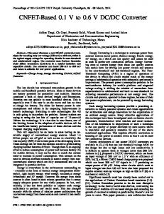
Introduction: CMOS devices have the important feature that they are easily scaled. Scaling down the transistor sizes enables integration of more circuit components in a single chip so that the circuit area, and thus its cost, will be reduced. However, scaling down also leads to MOS transistors with thinner gate oxides; and, to prevent the transistor from breakdown because of the higher electrical field across the thinner gate oxide and to ensure its reliability, the supply voltage has to be reduced. Lowering the supply voltage is also one of the most effective ways of reducing power consumption. However, many of the existing CMOS analogue building blocks, designed to operate with higher supply voltages, will lose a significant amount of operating range and need to be reconsidered. In this Letter, a new idea to solve this problem at low-voltage operations is proposed; moreover, this idea also improves the performance of the exponential voltageto-voltage converter (EVVC), therefore high performance EVVC at low-voltage low-power application is achieved.
which is drawn for the constant a¼0.1. Otherwise, the deviation of (1) from the ideal exponential function will increase drastically. As a result, the dB linear range as well as the input range is critically limited. In this Letter, the variable x is considered as a function of t as depicted in Fig. 1b, the x is relatively linear function of t for jtj � 5 (i.e x¼t). In this region, from (1) the f (x)¼f (t) is closed to the ideal exponential function as depicted in Fig. 1a by the dashed and circle symbol lines. Otherwise, x is a nonlinear function of t as shown in Fig. 1b by the circle symbol line (let x¼f1(t)). Intuitively, from (1) one can see that the equation f (x) ¼ f [ f1(t)] as a function of t is shifted to the ideal exponential function as shown in Fig. 1a by the circle symbol line, leading to the improvement of both the dB linear output range and the input range. In this Letter, the variable x and t are chosen to be current and differential input voltage parameters, respectively. Hence, the output voltage f (x) is a function of the differential input voltage t.
Low-voltage low-power EVVC design: Fig. 2 shows the schematic of the proposed EVVC that implements (1) and the proposed idea. As shown in Fig. 2, the voltage-to-current converter (VCC) is a differential amplifier with M3 and M4 as diode connected loads. Neglecting the second-order effects and assuming that all transistors are biased in the saturation region, the drain current of transistor M1,2 is given as � �� � 1 mn Cox W ðVin� þ Vcm � Vp � VTH Þ ð2Þ I1;2 ¼ 2 L where Vcm and VTH are, respectively, the common-mode input voltage and the threshold voltage of M1,2. The Vcm is chosen to bias M1,2 in the saturation region. The I1,2 are, respectively, copied to M5 and M6,7 by a multiplication factor of a constant k. The two output currents I of the VCC as shown in Fig. 2 are given as I ¼ k(I1 � I2) From (2), I is calculated as I ¼ kðI1 � I2 Þ ¼ bðVinþ � Vin� Þ ¼ bVd
ð3Þ
where b ¼ k (mnCoxW=L)(Vcm � Vp � VTH) and Vd ¼ Vinþ in Vin�. Equation (3) shows that the output current of the VCC, I, is linear function of Vd. The current I is, respectively, added and subtracted to the bias current I0 to form two current signals, (I þ I0) and (I � I0) as shown in Fig. 2. The current (I þ I0) is copied to the drain current of the transistor M14, while the current (I � I0) is fed to the drain of two diode connected transistors M11 and M12. As in [2] the transistors M11 and M12 constitute the linear I–V converter, and the output voltage of this converter is given as [2] VG;M11;12 ¼
VDD � jVTp j þ VTn ðI � I0 Þ � KðVDD � jVTp j � VTn Þ 2
ð4Þ
where VG,M11,12 is the output voltage of this converter which is also the gate voltage of transistor M15. The transistor M15 is assumed to be in the triode region and acts as a voltage controlled resistor. For small drain-source voltage, the resistance exhibited by M15 is given as RDS;M15 ’
Fig. 1 Various functions on dB scale, and variable x as linear and nonlinear functions of t
Proposed idea: EVVCs are usually implemented with bipolar or MOS transistors in weak inversion, because of their exponential I–V characteristics. However, bipolar transistors are not compatible with CMOS technology, and MOS transistors in weak inversion are limited to low-frequency applications because of their poor frequency response. Consequently, the ‘pseudo-exponential’ generators [1, 2] and the Taylor series approximation [3, 4] have been introduced as alternatives. The pseudo-exponential function is given as eax 1 þ ax ffi e�ax 1 � ax
ð5Þ
Consequently, the current (I þ I0) flowing through M15 will generate a drain-source voltage, VDS,M15 ¼ RDS,M15(I þ I0), proportional to (I þ I0)=(I � I0). Hence, the following equation applies
a Functions on dB scale b Variable x as linear and nonlinear functions of t
f ðxÞ ¼ e 2ax ¼
1 KM12 ðVG;M11;12 � VTH Þ
ð1Þ
where a and x are the coefficient and the independent variables, respectively. Equation (1) is valid for jaxj � 1. Using MATLAB to investigate (1), the results show 15 dB linear range with the linearity error < �0.5 dB for jxj < 0.42 as shown in Fig. 1a by the dashed line,
Vout ¼ VDS;M15 ’ M
I þ I0 I � I0
ð6Þ
where M is a constant. I1 is a function of the input differential voltage Vd ¼ Vinþ � Vin�. Finally, from (6) the pseudo-exponential approximation of the proposed circuit shown in Fig. 2 is given as Vout ¼ M
kVd þ I0 kV =I þ 1 ¼M d 0 kVd =I0 � 1 kVd � I0
ð7Þ
In (7), the output voltage Vout is obviously a pseudo-exponential function of the Vd, which is the same form of expression as in (1), where a ¼ k=I0. The I–V performance of the VCC is shown in Fig. 3. When the supply voltage is reduced as shown in Fig. 3 by the solid line, as Vd increases to saturate either input transistors in the differential pair, the
ELECTRONICS LETTERS 19th August 2004 Vol. 40 No. 17
linear relation of I ¼ bVd no longer exists because of cutoff or weak inversion operation of either transistor. This results in a narrow window for differential-input voltage at low-voltage applications. Therefore, for the VCC to achieve large differential-input swing as shown in Fig. 3 by the dashed line, the supply voltage should be high; however, the power consumption is high as well. This issue is not compatible for lowvoltage low-power applications. Fortunately, the idea in this Letter not only opens up a possibility to implement the I–V characteristic of the VCC at low-voltage applications but also extends the output range of the EVCC; hence, this idea is significant.
Fig. 4 V-V performance of EVVC shown in Fig. 2
Fig. 2 Proposed exponential voltage-to-voltage converter ( EVVC)
By implementing circuits that also replicate (1), some of the previously reported EVCCs have been able to obtain 15 dB of amplitude variation with the error < � 0.5 dB [1, 2]. However, these circuits have single inputs, and the dB linear ranges are extremely limited. The circuit proposed can extend the dB linear range drastically. Moreover, the circuit provides rail-to-rail differential input, which is useful for the design of analogue and mixed-signal circuits such as log-domain filtering, AGC, etc. Conclusions: We propose a new and compact EVVC that can operate at extremely low-voltage low-power applications and increase the output voltage range drastically (16 dB linear range improvement compared to traditional pseudo-exponential approximations [1, 2]). The proposed circuit offers significant performance advantages over previous works [1–4], such as high dB linear range, low-power (