The resort to LTCC technology permits us to improve the structure bulk by adding capacitive posts in the middle of the cavity. I/O CPW feeds are printed on the ...
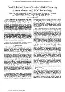
LTCC reduced-size bandpass filters based on capacitively loaded cavities for Q band application P.Ferrand1, D. Baillargeat1, Member, IEEE, S. Verdeyme1, Member, IEEE, J. Puech2, M. Lahti3, T. Jaakola3 1
IRCOM-UMR 6615-CNRS, Faculté des sciences de Limoges, 87060 Limoges Cedex, France 2 3
CNES, 18 avenue Edouard Belin 31401 Toulouse cedex4, France
VTT ELECTRONICS , P.O. Box 1100 Kaitoväylä 1 FIN-90571 Oulu Finland
Abstract — The filter presented here is composed of cavities delimited in a LTCC substrate by a periodic lattice of metallized via-holes. The resort to LTCC technology permits us to improve the structure bulk by adding capacitive posts in the middle of the cavity. I/O CPW feeds are printed on the top face of the substrate and are suitable for planar circuit integration. A filter, functionning around 42.6 GHz with bandwidth at –3dB of 7% and insertion losses lower than –0.6 dB has been designed and realized with success. Index Terms — LTCC, bandpass filter, periodic structures, capacitive post
by a periodic lattice of metallized via-holes. The substrate is made of six 99 µm thick layers of Ferro A6S (εr=5.9). Applying a 3D electromagnetic simulation, we optimize a cavity operating on a TM110 around 42.6 GHz (Fig. 1).
I. INTRODUCTION LTCC is a multi layer technology which use ceramic tape sheet layers stacking. Each layer is processed independently (conductors and via-holes) before being laminated and cofired in a monolithic multilayer substrate. It enables high precision 3D structuring and vertical integration of the circuit, and thus, showed great interest in reducing circuit bulk and improving circuit elements interconnections. The work presented in this paper is the result of a collaboration between IRCOM and VTT Electronic Finland within the frame of the LOTTO project which goal is to develop 40 GHz filtering solutions for telecommunication modules. The design of the filters takes place at the IRCOM and VTT realized the circuits. We have searched to apply the quasi-planar cavity concept based on periodic structures to the LTCC environment. Via-holes which are usually used to connect conductors through two layers are here arranged in a periodic lattice through all the substrate thickness to confine electromagnetic field in a resonant dielectric cavity. The 3D integration potential of LTCC permits us to improve resonator compactness by using a capacitive metallized post located in the middle of the cavity. II. Q BAND RESONATOR DESIGN A. LTCC resonator In [1], it was shown that an array of metallic via-holes could be used to confine the electromagnetic field in a dielectric substrate. The purpose of this part is the conception of a resonator composed of a cavity delimited in a LTCC substrate
Fig. 1.
Schematic of the LTCC resonator, dimensions are mm
Internal dimensions of the cavity are 2.1 x 2.1 mm² B. Capacitively loaded resonator The concept of adding capacitive effect to a resonator in order to modify its caracteristics has already been studied for different technologies and topologies [2,3,4,5]. In the work described in this paper, a non emerging via-hole located in the middle of the cavity is used to modify the resonant frequency of the cavity (Fig. 2).
Fig. 2. TM110 E field distribution in the cavity loaded with a capacitive post
This modification of the cavity geometry takes place where the electric field is maximal (TM110) and a capacitive effect appear between the cavity upper metallized face and the top of the via-hole (Fig. 3).
The addition of a metallized crown at the top of a constant 500 µm height post also enable the frequency tuning by the mean of its surface sizing (Fig.6).
Fig. 3. Schematic side view of the cavity showing the localisation of the capacitive effect
In this case, by using an equivalent lumped element RLC circuit of the unloaded cavity behaviour around the resonant frequency of the TMM110 mode, we can define the new frequency of the loaded cavity by adding the capacity Cd to the CR capacity. A new lumped element equivalent circuit is then defined as shown in figure 4, and the resonant frequency is given by the well known formula (1). Fig. 6. Radius of the metallized crown (R) versus resonant frequency and unloaded quality factor for a 500 µm height metallized via-hole
(1)
Fig. 4. Modelisation of the capacitive effect on a RLC lumped elements circuit
Therefore, we can observe the effect of this geometric modification of the cavity on the resonant frequency which decrease. The resonant frequency of a cavity fitted with a capacitive post is lower than for an equal size cavity without the post. That is to say that at equal functionning frequencies, a cavity with a capacitive post present lower dimensions than a classic cavity. The strengh of the capacitive effect depends on two parameters : the distance d between the top of the post and the top of the cavity and the top surface of the post. We have investigated two ways of adjusting the resonant frequency reduction. Fig. 5 shows the evolution of the resonant frequency and the unloaded quality factor versus via-holes height.
The strengthening of the capacitive effect go with a reduction of the unloaded quality factor due to losses increase above the top of the post where electric field is extremely concentrated. With the help of previous studies, we optimize a 42.6 GHz cavity. Therefore, a 400 µm height via-hole without crown is used in order to keep a good compromise between frequency reduction and unloaded Q decreasing (Fig. 7).
Fig. 7. Schematic of the capacitive post loaded cavity optimized by E.M simulations
Internal dimensions of the optimized structure are 1.45 x 1.45 mm². We have highlighted a 52 % size reduction brought by the addition of the capacitive post. The estimated unloaded quality factor of 350 which is still better than classic planar topologies is reduced from 20 % compared to the unloaded cavity functionning at the same frequency. II. TWO POLE BANDPASS FILTER Fig. 5. Post height (h) versus resonant frequency and unloaded quality factor for a metallized via-hole of radius 75 µm
Two pole filter is obtained by associating two cavities as described previously. Filtering targets are a central frequency of 42.6 GHz with 7 % -3dB bandwidth. Applying a Chebychev type synthesis method, we define an external quality factor
Qext of 23 and a coupling coefficient between the resonators K12 of 0.046 needed to fulfil the objectives. A. Coupling coefficients Inter resonators coupling coefficient : K12 The coupling coefficient between the two resonators is tuned by the means of the two via-holes acting like an iris to separate the cavities [1]. The closer these via-holes are, the narrower the canal linking the two cavities is and the coupling coefficient K12 is. (Fig. 8) Fig. 10. Position of the excitation system (L) versus external Q factor Qext (E.M calculations)
B. Two pole filter design
Fig. 8. iris
Schematic of the two associated cavities with the coupling
Working on previous parametric studies, the whole filter dimensions are calculated The dimension of the coupling iris and the position of the coplanar pattern are chosen to achieve the Qext and K12 values provided by the synthesis. A short phase of optimization lead us to final dimensions given on Fig. 11.
A parametric study of this coefficient versus the distance d separating the via-holes has been carried out by the means of E.M calculations. The result of this study is given on Fig. 9
Fig. 11. Schematic of the optimized two poles filter (dimensions are given in µm)
Simulated S parameters of the filter confronted to the targeted filter response are shown on Fig. 12. Fig. 9. Evolution of the coupling coefficient K12 versus the iris size (d) (E.M calculations)
External Q factor : Qext This parameter is link to the location and dimensions of the input/output excitation system of the filter which is composed of CPW ports printed on the top of the substrate [1]. This system enable coplanar measurement of the circuit and make easy its integration to a planar environment. The CPW is short-circuited to provide a magnetic coupling with the TM mode of the cavity located below. Gap and central conductor dimensions are designed to fit to measurement probes. The influence of its position compared to the edge of the cavity has been investigated (Fig. 10)
Fig. 12. S parameters of the simulated filter (dotted lines) compared to the ideal filtering function given by the synthesis (solid lines)
This response is in good agreement with the theoretical response, provided by the synthesis. C.Realisation and measurements As we have said, the circuit is realized by VTT Electronics on a six 99 µm thick layers of Ferro A6S. The conductor lines were screen-printed using CN33-398 Ag conductor and CN33343 Ag via fill paste. The microstrip line was printed using 400-mesh screen meanwhile striplines and all ground layers were printed with 325-mesh screen. Typical width of microstrip and stripline was 500 and 150 µm, respectively. The diameter of via holes was 150 µm. The layers were laminated at pressure of 3000 psi and temperature of 70 °C for 10 min. The peak temperature of co-firing process was 850 °C and the duration was about 16 h [6]. Dimensions of the fabricated filter fit well with the awaited ones as we can notice on Fig. 13. Dimensions of the fabricated filter are 3.9 x 2.4 mm².
The measured response is satisfying and well fitted with the simulated one. The experimental filter exhibits the following performances : fo=42.6 GHz, ∆f-3dB= 7 % and very low insertion losses in the band equal to - 0.6 dB. III. CONCLUSION A small size quasi-planar dielectric 2 pole filter based on capacitive loaded cavities has been designed and realized. It exhibit great performances with 0.6 dB insertion losses on a 7% -3dB bandwidth around 42.6 GHz. The measures are very closed from the electromagnetic calculations and validate our design methodology. This technology and filter topology can be used to obtain narrow bandwidth filter behaviour. Indeed, we have estimated that a two pole filter with less than 1 dB insertion losses and an equi-ripple bandwidth of 1 GHz can be obtained using resonators with an unloaded Q of 350. Therefore, the LTCC technology can be an alternative solution for the design of cavity filter with great performances and is well suited to mass production. ACKNOWLEDGEMENT The authors wish to thank the French Space Agency (CNES) for its financial support. REFERENCES
Fig. 13. Picture of the fabricated filter (dimensions in mm)
Measurements were taken with a HP 8510C vector network analyser and a cascade probe station. A SOLT calibration was used from 35 GHz to 50 GHz. Measured results are presented on Fig. 14.
Fig. 14. S parameters of the mesured filter (solid lines) compared to the optimized filtering function given by the simulation (dotted lines)
[1] P. Ferrand et al., “Compact quasi planar silicon bandpass filters based on metallic periodic structure for Q and V bands applications” IEEE MTT-S Int. Microwave Symposium Digest. June 2004. [2] D. Deslandes and K. Wu, “Integrated microstrip and rectangular waveguide in planar form” IEEE Microwave and Wireless Components Letters, vol. 11, no. 2, pp. 68-70, Feb. 2001. [3] M. Simeoni, R. Sorrentino, S. Verdeyme, “The circular wirepatch resonator-theory, numerical analysis, and filter design application” Microwave Theory and Techniques, IEEE Transactions on ,Volume: 51 , Issue: 4 , April 2003 Pages:1187 - 1193. [4] M.Ito et al., “60 GHz band planar dielectric waveguide filters with cross coupling for flip-chip modules”, IEEE MTT-S International Symposium Digest 2002 [5] X. Gong, A. Margomenos, B. Liu, W. J. Chappell and L. P. B. Katehi, “High-Q Evanescent mode filters using silicon micromachining and polymer stereolithography (SL) processing” IEEE MTT-S Int. Microwave Symposium Digest. June 2004. [6] R. Valois, D. Baillargeat, S. Verdeyme, M. Lahti and T. Jaakola, “High performances of shielded LTCC vertical transitions from DC up to 50 GHz” European Microwave Conference, Amsterdam, October 2004.