arXiv:1702.00260v1 [physics.optics] 31 Jan 2017
Machine learning based compact photonic structure design for strong light confinement MIRBEK TURDUEV1,5,* , CAGRI LATIFOGLU2,5 , IBRAHIM HALIL GIDEN3,6 , and Y. SINAN HANAY4,5 1
Department of Electrical and Electronics Engineering, TED University, Ankara 06420, Turkey 2 Department of Industrial Engineering, TED University, Ankara 06420, Turkey 3 Department of Electrical and Electronics Engineering, TOBB University of Economics and Technology, Ankara 06560, Turkey 4 Department of Computer Engineering, TED University, Ankara 06420, Turkey 5 Photonic Networks Research Group, TED University, Ankara 06420, Turkey 6 Nanophotonics Research Group, TOBB University of Economics and Technology, Ankara 06560, Turkey * Corresponding author:
[email protected] Compiled February 2, 2017
Abstract
terparts, the optimized lens and coupler designs are easy-to-fabricate via optical lithography techniques, quite compact, and can operate at telecommunication wavelengths. The outcomes of the presented study show that machine learning can be beneficial for efficient photonic designs in various potential applications such as polarization-division, beam manipulation and optical interconnects.
We present a novel approach based on machine learning for designing photonic structures. In particular, we focus on strong light confinement that allows the design of an efficient free-space-to-waveguide coupler which is made of Si- slab overlying on the top of silica substrate. The learning algorithm is implemented using bitwise square Si- cells and the whole optimized device has a footprint of 2 µm × 1 µm, which is the smallest size ever achieved numerically. To find the effect of Si- slab thickness on the subwavelength focusing and strong coupling characteristics of optimized photonic structure, we carried out three-dimensional time-domain numerical calculations. Corresponding optimum values of full width at half maximum and coupling efficiency were calculated as 0.158λ and −1.87 dB with slab thickness of 280nm. Compared to the conventional coun-
Studies on subwavelength light focusing phenomenon are increasing over time due to immense needs of light energy enhancement via confining it to a narrow region [1, 2, 3]. Light focusing into a tight spot smaller than the wavelength of light may find place in various optical applications including nanolithography, optical microscopy, optical measurements and optical data storage. Especially, highresolution imaging and strong beam coupling can be achieved by using the light focusing effect beyond the diffraction limit [4, 5]. Various subwavelength focus1
ing lenses have already been developed using metasurfaces [6], plasmonics [7], metamaterials [8] and alldielectric materials [9] as well as exploiting superoscillation [10] and hypergrating techniques [11]. Conventional theoretical approaches may not fully provide analytical solutions for complex photonic structures. Furthermore, theoretically designed systems may not satisfy the feasibility and performance requirements such as compactness, efficiency, bandwidth and energy loss drawbacks. For this reason, different types of optimization algorithms such as evolutionary algorithm [9], inverse optimization [12], topology optimization [13], nonlinear search algorithm [14], and the direct binary search algorithm [15] have been implemented to design efficient photonic integrated structures. However, to the best of authors knowledge, this is the first time that machine learning algorithm is utilized to design photonic devices with desired optical properties. Machine learning has attracted much attention from both academia and industry recently. Researchers leveraged machine learning successfully in developing a self-learning robot which can withstand failures [16], predicting hepatitis B positive patients [17], improving components’ performances in optical communication systems [18], detecting malicious software automatically [19] and understanding ecological phenomena [20]. Well-known applications in industry include driverless cars, language translation services (e.g. Google translate), credit decision systems and anti-virus software. In all those diverse examples, the power of machine learning lies in accurate modeling and characterization of complex relationships within the systems. In this study, we propose using a machine learning algorithm to construct highly efficient and compact focusing lenses that are able to surpass the light diffraction limit. The algorithm we use is called Additive Reinforcement Learning Algorithm (ARLA) [21] and like all the machine learning algorithms, ARLA consists of two phases: training and inference. In the training phase, which consists of a number of rounds, ARLA generates random photonic structures, and records the optical performance of each random structure. Later in the inference phase ARLA uses the information collected in the training
phase to come up with a final layout. The details of ARLA can be found in [21], which combines the additive updates feature of the perceptron algorithm [22] and the reward for state idea of reinforcement learning [23]. However, we briefly explain the steps in ARLA as shown in Figure 1. In the upper diagram of the figure, operations in a single round are depicted. The training phase starts with creating a random photonic structure that needs to be mirror-symmetric along x-axis to obtain the focal point at the optical axis. That half of the structure is represented with a 10x10 binary matrix, where a 1 corresponds to Si- and 0 corresponds to air cells of 100nm x 100nm. Thus, the size of complete photonic structure equals 2 µm × 1 µm. Next, finite-different time-domain (FDTD) method is used to calculate full-width at half maximums (FWHM) and maximum side lobe levels (MSLL) of the focused light beam using MEEP [24]. Here, FWHM and MSLL values are arranged as inputs for the reward function, which is defined as: R = Rmax − (w1 × F W HM + w2 × M SLL). (1) In this expression, w1 and w2 represent weights that control the trade-off between FWHM and MSLL values. The objective of the design problem is to find a photonic layout that minimizes both FWHM and MSLL; when both FWHM and MSLL values approaches to zero, reward approaches to Rmax , which is an arbitrarily chosen constant that satisfies the following condition:
Rmax > (w1 × F W HM + w2 × M SLL).
(2)
In the second phase, the inference phase, ARLA calculates a cumulative reward matrix from the results obtained in the training phase. A round matrix is multiplication of the binary matrix evaluated and its reward. Then ARLA normalizes this matrix A by subtracting the minimum value from all the elements. Next, ARLA applies a step function, which is shifted by the mean of A′ , to convert the normalized matrix A′ to a binary matrix. Finally, the binary matrix is converted back to a photonic structure, and this final 2
Figure 1: Flowchart of ARLA optimization algorithm for subwavelength light focusing purpose. structure is the final output of the algorithm, as can ing structure can be related to constructive interferbe seen from the inset in the figure. ence of propagating waves [25]: The optimized turThe number of training rounds N depends on the bid structure is perturbed in bitwise-scale so that desired focusing performance and the size of the pho- nanoscale local modifications exist in the correspondtonic structure. In our study that number was chosen ing refractive index distribution. The incident wave, empirically. Due to independent nature of the train- then, encounters multiple light scattering while proping rounds, ARLA can be fully parallelizable. We agating through the structure. Such scattering mechdistributed the training rounds to 12 different virtual anism enhances the constructive interferences at the machines each having two virtual CPUs and 3.75 GB output so that a strong light focusing may emerge RAM. ARLA can work with larger matrices as well, [26]. at the cost of increased training times.
The optimized lens design is constructed on a silicon-on-insulator (SOI) substrate and composed of Si- slab having the refractive index of nSi = 3.47, see Fig. 2(a). Corresponding geometrical parameters of the lens structure are represented as an inset in the same figure. The width and height of photonics lens are equal to {W, L} = {2 µm, 1 µm}. 3D FDTD calculations are carried out for the optimized structure in order to analyze the effect of Si- slab thickness on the subwavelength focusing performance [27].
The output of ARLA gives an optimized structure with the highest reward providing the subwavelength focusing effect, which is schematically drawn as inset in Fig. 1. The dielectric medium is optimized in bitwise scale via the machine learning ARLA method in order to control the near-field strong focusing effect, see the corresponding steady-state electric field Ez distribution in the same figure. Obtained subwavelength focusing effect through the optimized scatter3
(b) 300
100 nm
(c) 1.5 0.40
250
W
0.40
200
0.35 150
0.30
y
0.20
L
x
SiO 2
50 1.30
0.8
0.5 0.6 0 0.4
-0.5
0.25
100
z
1
0.45 FWHM ( λ)
Slab Thickness (nm)
Si
y-axis (μm)
H
1
1.35
1.40 1.45 1.50 Wavelength (μm)
1.55
0.2
-1 -1.5 1.30
1.60
Field intensity (a.u.)
(a)
0 1.35
1.40 1.45 1.50 Wavelength (μm)
1.55
1.60
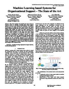
Figure 2: (a) Optimized bitwise photonic structure design as a near field sub-wavelength lens. (b) FWHM map depending on the slab thickness and incident wavelength variations. (c) The cross-sections of field intensities are taken at the output and plotted as a map depending on the incident wavelengths. FWHM values are calculated at the output face of the optimized design with respect to the variations of slab thicknesses H and the incident wavelengths with transverse magnetic-like (TM-like) polarization. This relationship is plotted as a FWHM map in Fig. 2(b). The calculated map shows that the excited light focuses with FWHM values below 0.20λ while the slab thickness to be in the range of 250nm-300nm. Furthermore, the minimum FWHM value was calculated as 0.155λ, which implies that the diffraction limit of light could be defeated in the near-field by the help of the optimized design. To be compatible with SOI technology and optical communication systems, the slab thickness of the optimized structure is fixed to H=280 nm.
the Fig. 2(c) and Fig. 3 (see inset plot) that incident beam is concentrated into a narrower spot with almost negligible levels of additional undesired side lobes. To quantify the broadband subwavelength focusing effect of the optimized lens structure, the slab thick-
0.20
1
Intensity (a.u.)
0.8
0.19
0.6 0.4
FWHM= 0.158λ
FWHM ( λ)
0.2
In order to show the broadband subwavelength focusing effect of the designed photonic lens, corresponding transverse cross-sections of output electric field intensities were calculated for varying incident wavelengths ranging between 1.3µm − 1.6µm and superimposed in Fig. 2(c) as a transverse crosssectional intensity map. It should be noted that, while dealing with the strong light focusing effect, it is crucial to consider the emergence of side lobes. Excessive side lobe radiations cause the reduction of the main lobe, which is undesirable for strong light focusing. Therefore, a main purpose of using machine learning is to suppress the intensity levels of the MSLLs besides of minimizing the FWHM values at the focal point. It can be clearly observed in
0 -1.5
0.18
-1
-0.5 0 0.5 y-axis (μm)
1
1.5
λ=1.51 μm 0.17 0.16 0.15 1.30
1.35
1.40 1.45 1.50 1.55 Wavelength (μm)
1.60
Figure 3: Calculated FWHM values depending on incident light wavelengths of the photonic slab lens having H = 280nm thickness. Steady state electric field profile with its transverse cross-sectional intensity profile at λ = 1.51µm are given as insets. 4
Slab Thickness (nm)
Si
W
250
0.5 0.4
200
0.3
150
0.2 100
z y
L
x
SiO 2
0.1 50 1.30 1.35
(c) 1.5
0.6
λ =1.55 μm 0.8
0.5 0.6
0 0.4
-0.5 0.2
-1 -1.5 -2
1.40 1.45 1.50 1.55 1.60 Wavelength (μm)
1
λ =1.35 μm
1
Field intensity (a.u.)
(b) 300
H
y-axis (μm)
200 nm
Normalized transmission
(a)
-1.5
-1
-0.5 0 0.5 x-axis (μm)
1
1.5
2 -2
-1.5
-1
-0.5 0 0.5 x-axis (μm)
1
1.5
2
0
Figure 4: (a) Optimized photonic structure design for air-to-waveguide coupling application. (b) Corresponding transmission efficiency map depending on the slab thickness and incident wavelength variations. (c) Spatial field intensity distributions of optimized structure calculated for the incident wavelengths of λ = 1.35µm (left) and λ = 1.55µm (right). The dashed boxes represent the structure boundaries. ness is fixed to H=280 nm and the FWHM values of the focused beam are calculated within telecom wavelengths. Corresponding FWHM plot is represented in Fig. 3. As can be seen from the figure, calculated FWHM values were less than 0.197λ, where the minimum value of FWHM was calculated as 0.158λ at operating wavelength λ = 1.51µm. The spatial electric field intensity profile with its transverse crosssectional plot is calculated at λ = 1.51µm and given as insets in the same figure. The FWHM plot shows that the optimized structure provides a broadband subwavelength focusing effect under λ/6 within the telecom wavelengths. Such strong subwavelength focusing property as well as small footprint size imply that the optimized photonic lens can also be considered as an alternative and promising solution for freespace-to-waveguide optical coupling applications. In addition, the optimized structure is all-dielectric so that such a photonic device is free of absorption losses and it may operate in a broadband regime comparing to its metamaterial and plasmonic counterparts [28, 29]. The coupling effect is also investigated in detail in the study using proposed machine learning based photonic lens. The optimized photonic lens device can also be applied for free-space-to-waveguide coupling problems. For this reason, Si- bulk waveguide with the width of 200nm is butt-coupled to the back face/output of the structure. 3D representation of the optimized free-space-to-waveguide coupler is represented in Fig. 4(a). The thicknesses of Si- slab and coupled waveguide are scanned in the range of 50nm-300nm
to analyze the coupling efficiency depending on the slab thickness. Free-space-to-waveguide coupling efficiency of the optimized structure is plotted according to the variation of incident wavelengths’ and given as a transmission map in Fig. 4(b). As can be seen from the map, the coupling efficiency of above 50%(−3dB) is obtained in the case of the slab thickness greater than 250nm. In the case of setting the coupler thickness to 280nm, the corresponding coupling efficiency was calculated to be around 65%(−1.87dB) within S (short wavelengths) and C (erbium window) wavelengths. Fig. 4(c) demonstrates steady-state spatial intensity profiles of the optimized coupler having 280 nm thickness for the incident wavelengths of λ = {1.35µm, 1.55µm}. The optimized coupler and the output waveguide are shown as dashed boxes in the figure. It can be inferred from the field intensity calculations in Fig. 4(c) that the proposed coupler design strongly confines the light to the output waveguide with ten times smaller width. In other words, the designed coupler transfers light energy from 2µm width waveguide to 200nm waveguide (with beam compressing ratio of 10:1) with 65% coupling efficiency. In conclusion, all-dielectric subwavelength focusing lens and air-to-waveguide coupler were designed utilizing machine learning for the first time. The performance of optimized photonic structure was analyzed employing 3D FDTD numerical calculations. The footprint of whole optimized system is 2 µm × 1 µm, which is thought to be very compact compared to the 5
[7] Fangwei Ye, Dumitru Mihalache, Bambi Hu, and Nicolae C Panoiu. Subwavelength vortical plasmonic lattice solitons. Optics letters, 36(7):1179–81, 2011.
other systems in the literature. A minimum FWHM value of 0.158λ and a maximum coupling efficiency of −1.87dB were calculated for the optimized photonic structure with the slab thickness of 280nm. The obtained sub-wavelength light focusing and strong coupling effects can be can be useful in various application domains such as medicine, optical communication, sensing structures and high precision optical device designs. Funding. The authors acknowledge the partial financial support of NATO SPS research grant No: 985048. Acknowledgement. The authors would like to thank Emre Bor for his helpful comments during the optimization process.
[8] Akash Kannegulla and LiJing Cheng. Subwavelength focusing of terahertz waves in silicon hyperbolic metamaterials. Optics Letters, 41(15):3539, 2016. [9] E Bor, M Turduev, and H Kurt. Differential evolution algorithm based photonic structure design: numerical and experimental verification of subwavelength λ/5 focusing of light. Scientific Reports, 6, 2016. [10] Fu Min Huang and Nikolay I. Zheludev. Superresolution without evanescent waves. Nano Letters, 9(3):1249–1254, 2009.
References
[11] [1] E Betzig, J K Trautman, T D Harris, J S Weiner, and R L Kostelak. Breaking the diffraction barrier: optical microscopy on a nanometric scale. Science (New York, N.Y.), 251(5000):1468–70, 1991. [12]
Sukosin Thongrattanasiri and Viktor A Podolskiy. Hypergratings: nanophotonics in planar anisotropic metamaterials. Optics letters, 34(7):890–2, 2009. Jesse Lu and Jelena Vuˇckovi´c. Nanophotonic computational design. Optics Express, 21(11):13351, 2013.
[2] J. B. Pendry. Negative refraction makes a perfect lens. Physical Review Letters, 85(18):3966–3969, [13] P Borel, A Harpoth, L Frandsen, M Kristensen, 2000. P Shi, J Jensen, and O Sigmund. Topology optimization and fabrication of photonic crys[3] Xiang Zhang Nicholas Fang, Hyesog Lee, Cheng tal structures. Optics express, 12(9):1996–2001, Sun. SubDiffraction-Limited Optical Imaging 2004. with a Silver Superlens Nicholas. Science, 308(2005):534–537, 2005. [14] Bing Shen, Peng Wang, Randy Polson, and Rajesh Menon. Integrated metamaterials for effi[4] Zubin Jacob, Leonid V. Alekseyev, and Evgenii cient and compact free-space-to-waveguide couNarimanov. Optical Hyperlens: Far-field imagpling. Optics express, 22(22):27175–82, 2014. ing beyond the diffraction limit. Optics Express, 14(18):8247, 2006. [15] Bing Shen, Randy Polson, and Rajesh Menon. Integrated digital metamaterials enables ultra[5] Alexander Poddubny, Ivan Iorsh, Pavel Belov, compact optical diodes. Optics Express, and Yuri Kivshar. Hyperbolic metamaterials. 23(8):10847, apr 2015. Nature Photonics, 7(12):948–957, 2013. [16] Antoine Cully, Jeff Clune, Danesh Tarapore, and [6] Nanfang Yu and Federico Capasso. Flat optics Jean-Baptiste Mouret. Robots that can adapt with designer metasurfaces. Nature Materials, like animals. Nature, 521(7553):503–507, may 13(2):139–150, 2014. 2015. 6
[17] Q. H. Ye, L. X. Qin, Marshonna Forgues, Ping [26] Allard P. Mosk, Ad Lagendijk, Geoffroy Lerosey, and Mathias Fink. Controlling waves in space He, Jin Woo Kim, Amy C. Peng, Richard Simon, Yan Li, Ana I. Robles, Yidong Chen, Z. C. and time for imaging and focusing in complex Ma, Z. Q. Wu, S. L. Ye, Y. K. Liu, Zhao Y. media. Nature Photonics, 6(5):283–292, 2012. Tang, and Xin Wei Wang. Predicting hepatitis Lumerical Solutions. B viruspositive metastatic hepatocellular carci- [27] Lumerical Solutions. http://www.lumerical.com/tcad-products/fdtd. nomas using gene expression profiling and supervised machine learning. Nature Medicine, [28] M Turduev, Z Hayran, and H Kurt. Fo9(4):416–423, apr 2003. cusing of light beyond the diffraction limit by randomly distributed graded index pho[18] Darko Zibar, Molly Piels, Rasmus Jones, and tonic medium. Journal of Applied Physics, Christian G. Schaeffer. Machine Learning Tech120(24):243102, 2016. niques in Optical Communication. Journal of Lightwave Technology, 34(6):1442–1452, mar [29] A G Nalimov and V V Kotlyar. Hyperbolic se2016. cant slit lens for subwavelength focusing of light. Optics Letters, 38(15):2702–4, 2013. [19] Konrad Rieck, Philipp Trinius, Carsten Willems, and Thorsten Holz. Automatic analysis of malware behavior using machine learning. Journal of Computer Security, 19(4):639–668, jun 2011. [20] JulianD. Olden, JoshuaJ. Lawler, and N.LeRoy Poff. Machine Learning Methods Without Tears: A Primer for Ecologists. The Quarterly Review of Biology, 83(2):171–193, jun 2008. [21] C ¸ Latifolu. Binary Matrix Guessing Problem. ArXiv e-prints, 1701.06167, jan 2017. [22] F Rosenblatt. The perceptron: a probabilistic model for information storage and organization in the brain. Psychological review, 65(6):386– 408, 1958. [23] R.S. Sutton and A.G. Barto. Reinforcement Learning: An Introduction. IEEE Transactions on Neural Networks, 9(5):1054–1054, 1998. [24] Ardavan F. Oskooi, David Roundy, Mihai Ibanescu, Peter Bermel, J. D. Joannopoulos, and Steven G. Johnson. Meep: A flexible freesoftware package for electromagnetic simulations by the FDTD method. Computer Physics Communications, 181(3):687–702, 2010. [25] D S Wiersma. Disordered photonics. Nature Photonics, 7(3):188–196, 2013. 7