1
Magnetic Josephson Junctions with Superconducting Interlayer for Cryogenic Memory Igor V. Vernik, Vitaly V. Bol’ginov, Sergey V. Bakurskiy, Alexander A. Golubov, Mikhail Yu. Kupriyanov, Valery V. Ryazanov and Oleg A. Mukhanov Abstract— We investigate Magnetic Josephson Junction (MJJ) – a superconducting device with ferromagnetic barrier for a scalable high-density cryogenic memory compatible with energyefficient single flux quantum (SFQ) circuits. The superconductorinsulator-superconductor-ferromagnet-superconductor (SIS’FS) MJJs are analyzed both experimentally and theoretically. We found that the properties of SIS’FS junctions fall into two distinct classes based on the thickness of S’ layer. We fabricate Nb-Al/AlOx-Nb-PdFe–Nb SIS’FS MJJs using a co-processing approach with a combination of HYPRES and ISSP fabrication processes. The resultant SIS'FS structure with thin superconducting S'-layer is substantially affected by the ferromagnetic layer as a whole. We fabricate these type of junctions to reach the device compatibility with conventional SIS junctions used for superconducting SFQ electronics to ensure a seamless integration of MJJ-based circuits and SIS JJ-based ultra-fast digital SFQ circuits. We report experimental results for MJJs, demonstrating their applicability for superconducting memory and digital circuits. These MJJs exhibit IcRn product only ~30% lower than that of conventional SIS junctions coproduced in the same fabrication. Analytical calculations for these SIS’FS structures are in a good agreement with the experiment. We discuss application of MJJ devices for memory and programmable logic circuits. Index Terms— Superconducting logic elements, memory devices, single flux quantum, RAM, energy efficient, proximity effect
I. INTRODUCTION
R
Single Flux Quantum (RSFQ) technology [1] offers unmatched clock speed and low power dissipation [2]-[4]. Recently, its power dissipation was further reduced with an introduction of energy-efficient single flux quantum logics [5]-[8], making these circuits viable contenders for the implementation of next generation high performance computing (HPC) [9], cryogenic sensor image processors, and high-end instrumentation. However to date, the high performance potential of RSFQ technology was realized only for limited practical applications of mixed signal Digital-RF circuits for communications and signal intelligence [10]-[12]. APID
I. V. Vernik and O. A. Mukhanov are with HYPRES, Inc. 175 Clearbrook Rd., Elmsford, NY 10523 USA (phone: 914-592-1190; fax: 914-347-2239; email:
[email protected]). V. V. Bol’ginov is with Institute of Solid State Physics, Russian Academy of Sciences, Chernogolovka, 142432 Russia (e-mail:
[email protected]). S. V. Bakurskiy and M. Yu. Kupriyanov are with Skobeltsyn Institute of Nuclear Physics, Moscow State University, Moscow, 119992 Russia (e-mail:
[email protected]). A. A. Golubov is with the Faculty of Science and Technology and MESA+ Institute for Nanotechnology, University of Twente, 7500 AE Enschede, The Netherlands (e-mail:
[email protected]). V. V. Ryazanov is with Institute of Solid State Physics, Russian Academy of Sciences, Chernogolovka, 142432 Russia and InQubit, Inc., 21143 Hawthorne Blvd., Torrance, CA 90503, USA (e-mail:
[email protected]).
Highly promising applications in HPC, instrumentation and other fields remain unfulfilled. The chief reason for this is a lack of dense, high capacity superconducting memory capable of matching unparallel clock speed and low power available with single flux quantum technology. In spite of substantial efforts to develop a suitable superconducting memory technology [13]-[21], only a 4 kbit random access memory (RAM) was demonstrated to date [16]. This capacity was not sufficient for practical applications. Serial memories applicable to some instrumentation applications [22] did not go further either, as a 1 kbit memory occupied a substantial area [23] making it hardly extendible to application requirements. Superconducting memory exhibits relatively low density due to relatively large size of SQUIDbased memory cells coupled to address lines via transformers which are difficult to scale [13]-[21]. Additionally, the RAM ac power was identified as an obstacle for the development of larger size memories [21]. In some cases, the lack of high capacity superconducting memory can be circumvented by architectural approaches reducing memory requirements [24]. An attempt to eliminate the need for massive addressable memories by the distribution of memory functions in digital RSFQ circuits is described in [25]. However an existence of dense energy-efficient random access memory would unlock many presently not realized applications and would substantially enlarge the applicability of superconducting technologies. In order to get around the low capacity of superconductor memories, hybrid superconductor-semiconductor schemes were pursued combining room-temperature CMOS memory and RSFQ interface circuits [26] or building a cryogenic (4 K) hybrid Josephson junction (JJ) CMOS RAM [27]. Recently, a cryogenic 64 kbit hybrid JJ-CMOS RAM was successfully demonstrated [28]. This hybrid RAM can fill a niche in the memory hierarchy, in which access time requirements are less demanding. Still, there is a strong need for a fast, energy efficient memory integrated with energy-efficient digital circuits on the same chip and capable of operating with a clock rate similar to RSFQ digital circuits. The ideas of combining superconducting and ferromagnetic materials to build a high density cryogenic RAM were first expressed in the 90s and recently gained even more attention [29]-[33]. These ideas were based on various structures of superconducting and ferromagnetic layers, ferromagnetic dots, combined with superconducting-isolator-superconducting (SIS) JJs for readout. However, these initial concepts were not further developed. A hybrid superconducting-magnetic RAM was proposed by combining proven magnetic tunnel junctions (MTJs) with the SIS readout JJs to form a cryogenic MRAM [34]. The experimental realization of superconducting-
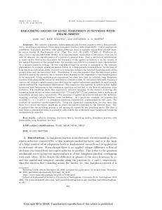
2 However, the fabricated SIS’FS showed significant differences in observed critical currents. From our initial measurements [46], it was difficult to establish whether superconductivity in the S’-layer was completely or only partially suppressed. In this paper, we theoretically and experimentally investigate SIS’FS junctions focusing on effects of the S’layer thickness. Our study is guided by requirements of these devices for memory applications and their compatibility to SIS-based digital circuits. II. SUPERCONDUCTOR-INSULARTOR-SUPERCONDUCTORFERROMAGNET-SUPERCONDUCTOR JUNCTIONS A. Theory Here, to analyze SIS’FS devices, the conditions of dirty limit are presumed to be valid for all superconducting and ferromagnetic layers. Additionally, the effective electronphonon coupling constant for the F is set to zero. With these assumptions, the critical current Ic is calculated by numerically solving Usadel equations [47] with Kupriyanov-Lukichev boundary conditions [48]. Figures 1-3 summarize the results of this self-consistent approach. Fig. 1 presents IcRn product as a function of F layer exchange energy, h, calculated at T=0.5TC for different thickness, LS’, of S’ film, large thickness of S electrodes and F layer thickness, LF=2 F with F being decay length in ferromagnet, of a SIS'FS sandwich. For simplicity, in our calculations the critical temperature, TC, for S and S’ layers is assumed to be the same with decay lengths S and S’ are, also, the same for all the films. All calculations are performed for SIS’FS structure with following layer thicknesses: for base S electrode of 2 S, for ferromagnetic layer of 2 F and counter S electrode of 10 S. Both S’F and FS interfaces can be described by suppression parameters γ=(ρS S)/(ρF F)=1, γB=(RS’FA)/(ρF F) =0.3, while suppression parameter at SI interface, γBI=(RNA)/(ρS S)=1000. Here ρS and ρF are resistivity of S, S’ and F films, respectively, RN and RS’F are the resistances of SI and S’F interfaces; and A is the area of junction cross section. 1
SIS
0- transition 0.1
|eICRn/2 TC|
ferromagnetic junctions in 1999 [35], [36] stimulated memory ideas based on using magnetic Josephson junctions (MJJs), in which ferromagnetic layers are integrated within a Josephson junction [37]-[46]. The MJJ critical current can change and retain its value by the ferromagnetic layer magnetization allowing the realization of two distinct states with high and low Ic, corresponding to logical “0” and “1” states, respectively. In [44], the storage MJJs are suggested to be integrated with readout SIS JJs into SQUID loops following known superconducting RAM architectures, e.g., [14]. However, it is not evident if MJJs in the proposed configuration can bring any advantage in density and energyefficiency as compared to the design with proven MTJs, cf. [34]. In contrast, the MJJs are suggested to perform both data storage and readout functions in [38]-[40], [45], [46]. The first MJJ-based memory with energy-efficient SFQ switching readout was proposed in [39], [45]. Such a memory required MJJs to be compatible in speed and critical currents with conventional SIS junctions. Memory built with these MJJs is electrically and physically compatible with SFQ-type circuits allowing a fabrication of memory and digital circuits on the same chip in a single process expandable to a high density 3D integration. This will enlarge the applications of MJJs beyond just memory arrays into programmable logic and enable the smaller footprint as SQUID loops are no longer required. Our MJJs are made using only one ferromagnetic layer (Flayer). By applying magnetic field pulses (e.g., by current pulses through a superconducting Write line), the junction Flayer can be magnetized in two opposite directions. To discriminate these directions, a read current bias is applied through the MJJ inducing a reference magnetic field (selffield). Depending on F-layer magnetization, this field either adds to or subtracts from F-layer magnetic field effectively forming two possible magnetic states with high or low magnetizations corresponding to low (“1”) and high (“0”) MJJ critical currents, respectively (see Fig. 2 in [46] for clarity). The switching between “0” and “1” states has been observed in Superconductor-Ferromagnetic-Superconductor (SFS) Nb/Pd0.99Fe0.01/Nb junction [38]. The characteristic voltage IcRn of these SFS devices was 2-3 nV, which makes them too slow (~MHz rate) for the memory designs discussed in [39]. Achieving MJJ switching speed comparable to that of conventional JJs is essential for both types of junctions to be integrated into a single circuit operating in an SFQ nonhysteretic switching regime. By inserting an additional isolation tunnel layer (I-layer) in the junction (i.e., fabricating an SIFS structure), we were able to increase Vc = IcRn to ~1 mV achieving high switching frequency. The SIFS MJJ based on Nb-Al/AlOx-Pd0.99Fe0.01-Nb tunnel junctions with Vc from 100 to 400 V were reported in [39]. Very recently, we demonstrated Nb-Al/AlOx-Nb-Pd0.99Fe0.01-Nb MJJ device of SIS’FS type where superconductivity of S’-layer was substantially affected by the adjacent ferromagnet making it close to the SIFS configuration [46]. By applying magnetic field pulses, the MJJ was switched between “0” and “1” logic states. This MJJ exhibited high characteristic voltage IcRn ~1 mV enabling fast non-destructive readout and making it applicable for an energy-efficient memory compatible to SFQ circuits.
S- S'- F -S 2-LS'-2-10
0.01
LS'=10
1E-3
1E-4
S
LS'=5
S
LS'=3
S
LS'=1
S
LS'=0.5
S
LS'=0.1
S
T=0.5 TC
0
5
10
15
20
25
30
35
40
45
50
55
60
h/TC Fig. 1. ICRn product of SIS’FS structure as a function of exchange energy h of F layer calculated for a set of thickness of S’ layer LS’ and T = 0.5 TC, LF=2 F, γ=1, γB= 0.3, γBI= 1000. Superconducting and ferromagnetic layer thicknesses are normalized to S and F, respectfully.
3 0.5
1
SIS
S-S' -F -S 2-Ls-2-10
0.4
|eICRn/2 TC|
|eICRn/2 TC|
0.1 S- S'- F -S 2-LS'-2-10 h=0 TC
0.01
h=10 TC h=20 TC h=40 TC
1E-3
near 0- transition h=5 TC
0.3
LS'=5
S
LS'=3
S
LS'=1
S
LS'=0.5
S
LS'=0.1
S
SIS h=0
0.2
0.1
T=0.5 TC
0
1
2
3
4
LS'/
5
6
7
8
S
0.0 0.0
0.2
0.4
T/TC
0.6
0.8
1.0
Fig. 2. ICRn product of SIS’FS structure as a function of thickness of S’ layer LS’ calculated for a set of exchange energy h and T = 0.5TC, LF=2 F, γ=1, γB= 0.3, γBI= 1000. Superconducting and ferromagnetic layer thicknesses are normalized to S and F, respectfully.
Fig. 3. ICRn product of SIS’FS structure as a function of temperature, T, calculated for a set of thickness of S’ layer and h=0, LF=2 F, γ=1, γB= 0.3, γBI= 1000. Superconducting and ferromagnetic layer thicknesses are normalized to S and F, respectfully.
In the limit of large LS’, the SIS’FS device can be considered as a composition of two independent SIS’ and S’FS junctions coupled in series. A flowing across SIS’FS supercurrent
junction critical current Ic = ISIS’ closes to that of AmbegaokarBaratoff (AB) theory (horizontal dashed line in Fig. 2), while the structure is either in 0- (h < 5TC) or in the π-state (5TC < h < 30TC) depending on the value of exchange energy, h (see Fig. 1). At lower thicknesses, the superconductivity in the layer S’ is suppressed due to the proximity effect. Fig. 3 presents the temperature dependencies of IcRn product calculated for different thickness, LS’, of S’ film, infinitely large thickness of S electrodes and F film thickness, LF=2 F, γ=1, γB=0.3, γBI=1000 and h=0. In a vicinity of Tc all the curves have a positive curvature. This behaviour is typical for SINS structures. It comes from suppression of superconductivity at SN interface and in the S’ layer, which is the stronger the closer is the temperature to Tc. For smaller T the intrinsic superconductivity in S’ film and at FS interface are restored. At LS’ > 3 S this is accompanied by strong increase of Ic to value, which is close to that followed from AB theory for SIS tunnel junctions (dashed line in Fig. 3). For LS’ = S the shape of Ic(T) is typical for SINS structures. It is proportional to (Tc – T)3/2 at T Tc and saturates for T = ETh, where ETh is Thouless energy [50]. The larger is h, the larger is the thickness of LS’ at which the crossover between this two typical shapes of Ic(T) occurs. In the interval of S’ layer thickness 3 S < LS’