interblock communication link in all of these schemes will con- ... it is possible to use simplified models in most cases to capture ... Restrictions apply. ... in this paper: to develop closed form equations for delay ... empirical equations have been developed which have reason- ..... They basically iteratively check for noise and.
224
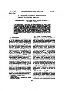
IEEE TRANSACTIONS ON VERY LARGE SCALE INTEGRATION (VLSI) SYSTEMS, VOL. 11, NO. 2, APRIL 2003
Maximizing Throughput Over Parallel Wire Structures in the Deep Submicrometer Regime Dinesh Pamunuwa, Li-Rong Zheng, and Hannu Tenhunen
Abstract—In a parallel multiwire structure, the exact spacing and size of the wires determine both the resistance and the distribution of the capacitance between the ground plane and the adjacent signal carrying conductors, and have a direct effect on the delay. Using closed-form equations that map the geometry to the wire parasitics and empirical switch factor based delay models that show how repeaters can be optimized to compensate for dynamic effects, we devise a method of analysis for optimizing throughput over a given metal area. This analysis is used to show that there is a clear optimum configuration for the wires which maximizes the total bandwidth. Additionally, closed form equations are derived, the roots of which give close to optimal solutions. It is shown that for wide buses, the optimal wire width and spacing are independent of the total width of the bus, allowing easy optimization of on-chip buses. Our analysis and results are valid for lossy interconnects as are typical of wires in sub-micron technologies. Index Terms—Bandwidth maximization, crosstalk, high performance, high-speed interconnect, interconnect delay, on-chip bus, repeater insertion, throughput maximization, wire optimization.
I. INTRODUCTION
M
OORE’S LAW has held remarkably true over the years and challenges at the device level have been and are being met with solutions of great ingenuity. It seems reasonable to assume that Moore’s law will continue to hold true over the next eight to ten years. The ability to put hundreds of millions of transistors on a single chip has, however, created new challenges for the systems engineer in dealing with the complexity in such a way that potential bottlenecks such as timing closure, power distribution, and input–output requirements are not allowed to dictate the ultimate size, and hence, the functionality of the chip. A potential solution is an on-chip packet switched network, which has been proposed by a number of authors [1]–[3]. Whether of a regular tiled nature or otherwise, the interblock communication link in all of these schemes will consist of a large number of parallel wires with uniform coupling over most of the wire length in all probability. This article examines signaling techniques and conventions over such relatively long coupled lossy lines, with emphasis on minimizing delay and maximizing bandwidth over multinet structures. A key question that we pose and attempt to answer in this paper is, given a fixed area in which to distribute the interconnect, what is the best arrangement of the wires to obtain Manuscript received February 5, 2002; revised June 19, 2002. This work was supported by the Swedish governmental funding agencies Sida, Vinnova, and Exsite. The authors are with the Laboratory of Electronics and Computer Systems, Department of Micro-Electronics and Information Technology, Royal Institute of Technology, Kista SE-164 40, Sweden. Digital Object Identifier 10.1109/TVLSI.2003.810800
the highest bandwidth? Is it to have a few fat wires and a high signaling frequency, or a large number of small wires with a lower signaling frequency, or anything in between? How does the wire spacing affect overall bandwidth? What effect does repeater insertion have? How many repeaters should there be and how should they be sized? Interconnects in deep submicron technologies are typically delay dominates. In order to keep the very lossy so that the resistance to a minimum, the aspect ratio (height/width) of wires is increased, which gives rise to increased interwire capacitance. This interwire capacitance results in crosstalk which has an effect on the delay, depending on how the aggressor lines switch. Crosstalk is of special significance in uniformly coupled parallel wires, causing unpredictable delays. A crucial point here is that when the geometry of the wire arrangement changes, the parasitics of the wires change in a highly nonlinear fashion. In particular, the exact manner in which the total capacitance is distributed into a ground component, and a component consisting of the capacitance to the adjacent wires is important, as this dictates the charging/discharging time. In the following sections, we carry out a novel analysis for optimizing bandwidth which maps the wire geometry to the parasitics, and uses modified switch factor based delay models that consider the effect of crosstalk on delay with good accuracy. Equations for optimizing the repeater size and number to compensate for the effects of switching aggressors are developed to aid in this analysis. We show that for a given metal resource in terms of a fixed total width, there is a clear global optimum consisting of a particular number of wires having a particular wire width and spacing. This optimum configuration does not necessarily translate to the maximum parallelism allowed by the technology, and in fact deviates considerably from it when the resources available for repeater insertion are limited. For wide buses, this optimal wire width and spacing is mostly independent of the total area. The main contribution of this paper is in providing an analysis of delay and bandwidth issues over multiple, long, capacitively coupled lossy nets, and deriving analytic guidelines for optimizing the wire width and pitch for maximizing total bandwidth. II. OVERVIEW An accurate analysis of interconnects requires solving Maxwell’s equations in three-dimensions (3-D), which is prohibitively expensive in terms of computation time. However, it is possible to use simplified models in most cases to capture the important effects in the regime of interest [4]. We present in this section a brief overview of parasitic modeling and delay
1063-8210/03$17.00 © 2003 IEEE
Authorized licensed use limited to: Lancaster University Library. Downloaded on November 30, 2009 at 05:28 from IEEE Xplore. Restrictions apply.
PAMUNUWA et al.: MAXIMIZING THROUGHPUT OVER PARALLEL WIRE STRUCTURES IN THE DEEP SUBMICROMETER REGIME
225
Fig. 1. Configuration for investigating effect of crosstalk. (a) Geometrical arrangement of the parallel multinet structure. (b) Electrical model for delay modeling comprising victim net capacitively coupled to two aggressors in a uniform and distributed manner.
modeling with emphasis on the suitability for our objective in this paper: to develop closed form equations for delay prediction in parallel wire structures that will aid in gaining an intuitive understanding of how changes in the wire geometry affect the delay. A. Parasitic Modeling The skin depth at the highest frequency of interest is usually high enough so that the DC resistance is quite accurate [5]
(1) If second-order effects are ignored, and the capacitance of a wire is modeled solely by its parallel plate capacitance, changing the width does not affect the RC delay, as a decrease (increase) in resistance by a certain factor is accompanied by an increase (decrease) in capacitance by the reciprocal of the same factor leaving the RC product unchanged, However, it is well known that for interconnects in sub-micron technologies, the higher aspect ratio results in the fringing component of the capacitance being of similar or often greater magnitude than the parallel plate component [6]. Hence, the RC delay does change with the wire width, and does so in a highly nonlinear fashion. Further, most of the fringing capacitance is to an adjacent conductor, which results in capacitive crosstalk. Hence, the accurate distribution of the total capacitance into self and mutual terms is very important. The parasitic capacitance is a very strong function of the geometry, and 3-D field solvers are required to obtain accurate values. However, over the years, empirical equations have been developed which have reason-
able accuracy, and are very important in gaining an intuitive understanding at a system level. The models can be broadly classified into those that consider an isolated rectangular conductor, and those that consider a multiwire structure. The geometrical parameters mentioned below can be identified by referring to Fig. 1. The models in the first category describe the self capacitance of the wire and an overview can be found in [7]. One of the early approaches detailed in [8] gives an empirical formula which decomposes the capacitance of a single rectangular wire over a ground plane into a parallel plate component and a component proportional to a circular wire over a ground plane, and hence, has a straightforward physical motivation. The accuracy falls of this equation however drops rapidly when the ratio below values of about 2–3. The trend in modern technologies is to have increasing numbers of metal layers, thus increasing , and shrinking wire sizes, decreasing , making the regime below this ratio the most interesting, and hence, rendering it unsuitable for on-chip wires. In [9], Sakurai reports (2) which was developed from curve fitting techniques, and is more accurate in the regime of interest
(2) Finally, in [10], another slightly more complex equation is presented for the configuration of a single wire, which is reported to be the most accurate in [7] for the values of dielectric m) and conductor thickness ( m) thickness ( that were used in the study.
Authorized licensed use limited to: Lancaster University Library. Downloaded on November 30, 2009 at 05:28 from IEEE Xplore. Restrictions apply.
226
IEEE TRANSACTIONS ON VERY LARGE SCALE INTEGRATION (VLSI) SYSTEMS, VOL. 11, NO. 2, APRIL 2003
For the configuration of a conductor surrounded by two adjacent wires, Sakurai in the paper cited above, defines a coupling as given in (3) capacitance (3) This is used to define a total capacitance for the middle con. The total capacitance given by ductor as the sum of and this equation is in very good agreement with that predicted by a field solver for the total capacitance of the middle wire, but the individual components are not intended to provide decomposition of the total into ground and coupled components. Since the presence of the adjacent conductors significantly affects the electric field around the central conductor, accurate decomposition requires that the proximity of the neighboring conductors, or in a mathematical sense the quantity , has to be modeled in the expression for the self capacitance. It then follows that the expressions for mutual capacitance are also unusable on their own.1 Hence, although these equations are quite useful for certain applications, they not suitable for a bandwidth analysis which requires that the distribution of the capacitance into self and mutual components be accurate. Since then, formulae which attempt to partition the total capacitance into two components accurately have been proposed, in [12] and [13] and more recently in [14] and [15]. The equations in [12] have been widely used in the past, but drop in accuracy when the aspect ratio of the wires increase to DSM proportions. The methodology proposed in [14] uses numerous technology dependent constants, which render the models rather difficult to use without familiarity with their derivation. The formulae proposed in [13] and [15] can be conveniently used for parasitic extraction of DSM geometries. The models in [15] use a single technology dependent constant, derived by generating a database of values with a field solver for different geometries in a particular technology, and then using curve fitting techniques. They are in effect a modification of Sakurai’s equations to render the partitioning more accurate. In this paper, these latter models will be used for mapping the wire geometry to the capacitive parasitics. They are reproduced in Section III-A. Extraction of inductive parasitics poses problems of a different nature altogether [5], and in fact there is a certain duality when compared with capacitance extraction. Capacitance is very localized in that the electric field lines from a given conductor tend to terminate on the nearest neighbor conductors. This makes the capacitance matrix sparse (since only the terms related to the coupling between close wires need be included, the others being insignificant), so that analytic formulae need only model the geometry of the wire in question and the adjacent wires. However, the nonzero interaction terms have a very strong geometry dependence. This makes the accuracy of analytic formulae somewhat limited, and an error contained to within roughly 10% is about the best that can be hoped for in the prediction of different capacitive components of complex structures. By contrast, strong geometry dependence does not exist for inductance and local calculation is rather easy, rendering an1An excellent discussion including independent verification of this can be found in [11].
alytic formulae for partial inductances quite accurate. But again, contrary to the situation with capacitance, the locality problem is much harder. Current loops defining flux linkages can, and often do, extend far beyond the conductor in question, making the inductance matrix very dense. Hence, sparsifying the inductance matrix is a difficult problem. Because of the relative insensitivity of signal waveforms to variations in the parasitic inductance though, expensive extraction techniques can be avoided to a fair extent for most circuits, with some approaches even adopting a constant precharacterized inductance [16]. B. Delay Modeling 1) Interconnect Modeling: From now on, whenever delay is mentioned without further qualification, we are talking about the 50% point of the step response, which is the delay to the switching threshold of an inverter. The most ubiquitous circuit model in MOS circuits is a lumped capacitance (representing the load) driven through a series resistance (representing the driver impedance), which has a single pole response and a delay as shown in (4) (4) One of the most prevalent methods of estimating the delay of more complex networks is to model the output by a single pole response, where the pole is the reciprocal of the first moment of the impulse response. This is often referred to as the Elmore delay, after the person who first proposed it as an upper bound to the delay in an analysis of timing in valve circuits [17]. Now, thin on-chip wires have a high resistance and are most often modeled by distributed RC lines. Signal propagation along such lines is governed by the diffusion equation which does not lend itself readily to closed-form solutions for the delay at a given threshold. However, it turns out that a first-order approximation results in very good predictions [18], [19]. One way of explaining this is to recognize that a distributed line (which comprises cascaded RC sections in the limit where the number of sections tends to infinity) is a degenerate version of an RC tree, with the step response in consequence having a dominant time constant. This time constant can be well approximated by the Elmore delay, or RC, which leads to (5) as the model for the delay of a distributed RC line [18] (5) This is a very good approximation and is reported to be accurate to within 4% for a very wide range of R and C. Sakurai in [20] reports a heuristic delay formulae based on a single pole response which predicts values which are very close to the elmore delay. A distributed RLC model is the most accurate depiction of a wire, but it is not possible to get exact analytic solutions for the delay. Numeric techniques based on convolution methods [21], [22] and moment matching techniques [23]–[25] have been proposed, where it is possible to calculate the delay to arbitrary accuracy, depending on the number of matrix manipulations. For timing driven layout optimization, however, simpler models are necessary. In [26], Kahng and Muddu present closed form equations for the delay of a distributed RLC line by consid-
Authorized licensed use limited to: Lancaster University Library. Downloaded on November 30, 2009 at 05:28 from IEEE Xplore. Restrictions apply.
PAMUNUWA et al.: MAXIMIZING THROUGHPUT OVER PARALLEL WIRE STRUCTURES IN THE DEEP SUBMICROMETER REGIME
ering the first and second moments of the impulse response. Ismail and Friedman in [27] give empirical closed form equations derived from curve fitting techniques. Particularly elegant in their model is the fact that setting the inductance term to zero makes it consistent with the RC tree delay. Now there are an increasing number of works that address the issue of when the effect of inductance is important enough to be modeled in the delay [28]–[32]. These expressions, though formulated in different ways, are for the most part equivalent. Reproduced here are the expressions from [29], because they neatly quantify a window where inductance is important, and have a straightforward physical motivation (6) A lossy transmission line has series resistive and inductive segments and parallel capacitive segments (the conductive loss to ground can be safely ignored for the vast majority of very large scale integration (VLSI) circuit applications). The symand in (6) refer to the per-unit length quantities while bols refers to the length of the wire. Now, in a qualitative sense, if the combined capacitive and inductive reactance at the highest frequency of operation (defined by the rise time at the output of the driver) is comparable with the series resistance, inductance cannot be ignored. This condition defines the second inequality of (6); if the line is longer, the loss is high enough to mask out the inductive effect. However, the line also has to be long enough for the delay at the speed of light in the medium to be comparable to the rise time; if not, the gating signal is too slow for the reactance to compete with the resistance. This defines the first inequality. Additionally, this window may never exist, if the combination of the rise time and loss is such that short lines have a time of flight delay that is much less than the rise time, and long lines have far too much loss for inductance to be important. This condition is defined in (7) (7) The inequalities (6) and (7) can be used to show that for the majority of nets in VLSI circuits, inductance can be safely ignored. In closely coupled lines the phenomenon of crosstalk can be observed. Crosstalk may be both inductive and capacitive. In coupled microstrip lines, for example, the mutual capacitance couples the time derivative of voltage while the mutual inductance couples the spatial derivative of voltage, so that a signal transition on one line may induce traveling waves on another line [33], [34]. For DSM circuits, capacitively coupled lossy lines are the most relevant when the phenomenon of crosstalk causes signal integrity and delay problems. Crosstalk couples a noise pulse onto the victim net which can have two effects: it can result in a functional failure by causing the voltage at a node to switch above or below a threshold, and it affects the propagation velocity of signal pulses on the victim line. In this paper, we are only concerned with the influence on delay. The effect of crosstalk on the delay depends on the switching of the aggressor lines, and can truly be captured only by dynamic simulators which takes into account arrival times of dif-
227
ferent signals and carries out a full transient analysis. It is possible, however, to limit the aggressor alignment to a few specific cases and develop timing models for static analyses. One such work is [35], where moment-matching techniques are used to obtain single pole responses for coupled lines. Most often static timing models, which take crosstalk into account are based on a switch factor. The capacitance for a line is modeled as the sum of two components, one of which represents the capacitance to ground, while the other represents the capacitance to adjacent nets. This second component is multiplied by a factor which takes the value of 0 and 2 for the best and worst cases, respectively. Kahng et al. in [36] show that 2 does not necessarily constitute an upper limit on the delay in general, where the inputs are finite ramps, and have different slew rates, and that 3 is a better factor for worst-case estimations in such situations. There have been works which have derived closed form equations for the delay where the capacitance has been distributed into two components. Examples are [37], which uses a lumped model, and [38], which uses a single section model and derives two pole delay models for arbitrary ramp inputs. However, when the wire length increases, the lumped model can result in large deviations from the actual delay. For example, for an isolated distributed line of 500 resistance and 100 fF capacitance with a 10 fF gate load driven with a driver having a Thevenin resistance of 1 k , the difference between the delay predicted by a single section model and a five section model is 41%. 2) Repeater Insertion: The most common method of reducing delay over long interconnects is to insert repeaters at appropriate points. Bakoglu and Meindl in [39] presented an analysis based on characterizing the repeater with an input capacitance and an output resistance which was one of the pioneering works in this area. Subsequently, researchers have improved on both the repeater model and the wire-load model. Wu and Shiau in [40] use a linearized form of the Schichmann–Hodges equations while Adler and Friedman in [41] use Sakurai’s alpha power model to include the effect of velocity saturation in short channel devices. In [42], Dhar and Franklin present an elegant mathematical treatment of area constrained optimization. Ismail and Friedman in [27] use the interconnect model mentioned above to carry out an analysis for repeater insertion which models inductance for the first time. As we mentioned at the beginning of this section, a clear distinction is made between crosstalk noise and crosstalk on delay effects. There have been a lot of articles published which propose efficient methodologies to insert repeaters to combat both effects [43], [44]. They basically iteratively check for noise and delay constraint violations, and insert repeaters where necessary, optimizing the placement in the process. The delay calculations in these methodologies are made with the switch factor based models, or higher order numeric models such as AWE described in [24]. There have been relatively few works which address the issue of driver modeling and optimizing the repeater size and number to combat the crosstalk on delay effect. One such work is [45], where the authors model the driver with a “transient” resistance which is calculated numerically. 3) Our Approach: Since our objective in this paper is to develop closed form equations for bandwidth optimization in parallel wires, we use analytic delay models that are very simple,
Authorized licensed use limited to: Lancaster University Library. Downloaded on November 30, 2009 at 05:28 from IEEE Xplore. Restrictions apply.
228
IEEE TRANSACTIONS ON VERY LARGE SCALE INTEGRATION (VLSI) SYSTEMS, VOL. 11, NO. 2, APRIL 2003
yet model with good accuracy the most important phenomenon in closely coupled wires: that of capacitive crosstalk. The lines are modeled as coupled uniformly distributed RC lines, and a slightly modified switch factor based analysis of delay in long uniformly coupled nets is presented, where the capacitance is distributed over two components and two empirical constants are used to appropriately modify the dominant time constant. This is shown to be more accurate than using a factor of 2 to model the worst case, although, the complexity is the same. We further use this model to show that both the number and size of repeaters can be optimized to compensate for dynamic effects. The Ismail metrics given above are utilized to verify the boundary conditions where these models are valid. These equations for repeater insertion give a very simple means of modeling the effect of crosstalk on delay and provide an insight at the system level into timing issues in long buses, allowing easy analysis of bandwidth optimization.
TABLE I COEFFICIENTS OF THE HEURISTIC DELAY MODEL FOR DISTRIBUTED LINE WITH DIFFERENT SWITCHING PATTERNS
For DSM circuits, typical geometries are well within this range. Additionally, the DC resistance is given by
III. INTERCONNECT MODELING AND DELAY ANALYSIS
(17)
The electrical model for investigating delay is shown in Fig. 1(b). Each line, except the two peripheral lines, are coupled on both sides to aggressors. The reason is that this is closest to the actual situation for an interconnect in a bus. This is a lossy capacitive model which does not include inductance, and is valid for the thin wires which are typical of DSM technologies. A. Parasitic Modeling To calculate the capacitance terms shown in Fig. 1 we use the models proposed in [15]. They use a technology dependent constant which is calculated from a database of values generated by a field solver, and are defined in (8)–(13) (8)
(9) (10) (11) (12)
B. Line Delay and Repeater Insertion In the delay analysis, the victim line is assumed to switch from zero to one, without loss of generality. When a line switches up(down) from zero(one) it is assumed to have been zero(one) for a long time. For simultaneously switching lines in the configuration of Fig. 1, six distinct switching patterns can be identified. 1) Both aggressors switch from one to zero. 2) One switches from one to zero, the other is quiet. 3) Both are quiet. 4) One switches from one to zero, the other switches from zero to one. 5) One switches from zero to one, the other is quiet. 6) Both switch from zero to one. Consider 3) above as the reference delay, where the driver of the victim line charges the entire capacitance. Cases 1) and 2) slow down the victim line, 4) is equivalent to 3), and 5) and 6) speed up the victim. In all cases except 5), the response of the distributed line for step inputs has a dominant pole nature.2 Since the time constants in question are linear combinations of and , changing coefficients are sufficient to distinguish between the different cases. The delay is as given in (18) where take the values in Table I (18)
(13) Typical values of range from 1.50 to 1.75, and 1.65 may be used for most DSM technologies. The equations are reported to be accurate to over 85% when the following inequalities are satisfied (14) (15) (16)
These constants were obtained by running sweeps with the circuit analyzer SPECTRE. Now the total delay of the line is affected by the driver strength, and the load at the end of the line. The simplest characterization of the driver is to consider it , with as a voltage source in series with an output resistance at the input. The linear approximation a capacitive load of 2The reason is that distributed, uniformly coupled RC nets resemble charge sharing networks, which often have a dominant pole on the signal path. However, if the dominant pole is not on the signal path, (from the driver of the victim to the load of the victim) or the network has two coincident poles, the response has a two pole nature [47].
Authorized licensed use limited to: Lancaster University Library. Downloaded on November 30, 2009 at 05:28 from IEEE Xplore. Restrictions apply.
PAMUNUWA et al.: MAXIMIZING THROUGHPUT OVER PARALLEL WIRE STRUCTURES IN THE DEEP SUBMICROMETER REGIME
229
TABLE II ACCURACY OF DELAY MODEL WITH EMPIRICAL CONSTANTS MEASURED AGAINST SPECTRE AND TRADITIONAL WORST CASE MODEL
of the buffers allows the use of superposition to find the delay, which is given by (19)
(19) combines with all the capaciThe lumped resistance tances (lumped and distributed) to produce delay terms with a coefficient of 0.7. Similarly, the distributed resistance of the line combines with various capacitances to produce different delay terms (it is assumed that the load at the end of the line is an inverter, which is the same size as the driving inverter). The terms which model crosstalk are shown in bold. The coefficient is a second empirical constant to model the Miller effect. Together, these two coefficients make the expression for total delay more accurate than using a single coefficient of 2 for the coupling , the above excapacitance to model the worst case. For pression reduces to (20)
(20) If a universal factor of 2 is used for the coupling capacitance, the expression takes the form given in (21)
(21)
Hence, with the empirical constants that we propose, factors of 4.4 and 1.5 appear before , while in a conventional worst-case analysis they would be 4 and 1.6. If the driver impedance is set to zero, the difference between the two expressions is very small, but with nonzero driver impedances, the difference is significant. The accuracy of (20) and (21) was checked against simulated values, and the results are presented in Table II, which is divided into three sections. The first section has parasitic values that can be said to represent those of global or semi-global wires, the second has values that are more typical of narrower wires, while the third has a much wider variation of all three parameters. The values corresponding to and were set to 1 k and 0, 3 k and 0, and 5 k and 100 fF for the three sections, respectively. The comparison is also plotted in Figs. 2–4. It can be seen that in all cases, the empirical model contains the error to under 5%, while the traditional method is more sensitive to the value of the driver impedance and has errors of up to 10% for certain cases. To reduce delay the long lines in Fig. 1 are broken up into shorter sections, with a repeater (an inverter) driving each section. Let the number of repeaters including the original driver be , and the size of each repeater be times a minimum sized inverter (all lines are assumed to be buffered in a similar fashion). The output impedance of a minimum sized inverter for the parand the output capacitance ticular technology is R both of which are assumed to scale linearly with size. This arrangement is sketched out in Fig. 5, where the symbol refers to
Authorized licensed use limited to: Lancaster University Library. Downloaded on November 30, 2009 at 05:28 from IEEE Xplore. Restrictions apply.
230
IEEE TRANSACTIONS ON VERY LARGE SCALE INTEGRATION (VLSI) SYSTEMS, VOL. 11, NO. 2, APRIL 2003
Fig. 2. Comparison of empirical and traditional switch factor based analyses. Points correspond to entries 1–27 of Table II.
Fig. 3. Comparison of empirical and traditional switch factor based analyses. Points correspond to entries 28–54 of Table II.
a capacitively coupled interconnect as shown in Fig. 1. In general, the line segments corresponding to the gain stages would not be equal in length, as repeaters are typically situated in “repeater stations,” the locations of which are determined by overall layout considerations. Then the delay is given by (22)
(22) It is assumed that the load C is equal to the input capacitance of an sized inverter. Also, the signal rise time has been included here. For the long lossy lines that we consider here, usually the delay of the line is much greater than the rise time
Authorized licensed use limited to: Lancaster University Library. Downloaded on November 30, 2009 at 05:28 from IEEE Xplore. Restrictions apply.
PAMUNUWA et al.: MAXIMIZING THROUGHPUT OVER PARALLEL WIRE STRUCTURES IN THE DEEP SUBMICROMETER REGIME
231
Fig. 4. Comparison of empirical and traditional switch factor based analyses. Points correspond to entries 55–81 of Table II.
Fig. 5.
Repeaters inserted in long uniformly coupled nets to reduce delay.
of the signal with which the driving inverter is gated, and the 50%–50% delay from buffer input to output interconnect node is independent of rise time [46].3 Now the minimum delay is obtained when the repeaters are equalized over the line, when the above expression reduces to (23)
(23)
When a number corresponding to a certain case is substituted for in the two equations, the number and size of repeaters to minimize the delay for that particular switching pattern results. is set to zero Note that when the coupling capacitance term (i.e., the entire capacitance is lumped into the term ), (7) and (8) simplify to the Bakoglu equations [19]. Thus, we have proposed a simple way to distribute the capacitance and take the effect of switching aggressors into account. These equations and their ramifications for repeater insertion strategies are examined in more detail later in the paper. C. Model Verification
In order to find the optimum and for minimizing delay, the partial derivatives of (23) with respect to and are equated to zero, resulting in (24) and (25) (24)
(25) 3This is assuming that zero time is when the driving inverter starts to switch. If zero time is considered to be the point at which the ramp to the first driver starts, the entire rise time should be added.
1) Aggressor Alignment: The effect of aggressor alignment (the times at which the aggressors switch relative to the victim net) on delay is a much researched topic [48]. For a three net arrangement such as was considered in this paper, it has been shown that when the slew rates are unequal, the worst-case delay is caused by aggressors which switch at different times [36]. Since our models are built up by considering simultaneously switching nets, and we present case 1) as being very near worstcase, it is interesting to check the inaccuracy introduced by our assumptions. Since we are analyzing uniformly coupled data lines, it is reasonable to make the simplifying assumption that the rise times
Authorized licensed use limited to: Lancaster University Library. Downloaded on November 30, 2009 at 05:28 from IEEE Xplore. Restrictions apply.
232
IEEE TRANSACTIONS ON VERY LARGE SCALE INTEGRATION (VLSI) SYSTEMS, VOL. 11, NO. 2, APRIL 2003
TABLE III COMPARISON OF MODEL FOR BUFFERED NET WITH WORST-CASE CROSSTALK AGAINST ACTUAL DELAY WITH REAL INVERTERS
Fig. 6. Eye diagram at the output of the victim net showing the effect of aggressor alignment on delay.
of the input signals are the same. Even for this simplified case, it is not simultaneous switching, but both aggressors switching slightly after the victim that causes the worst delay. This is, however, a very small difference and is really negligible. The effect of different aggressor alignment on delay can be seen by inspection of the eye diagram at the output of the victim net, built up over hundreds of cycles, with different pseudo-random bit streams (PRBS) being fed to the three lines. Consider a net , fF, and fF, where with and fF.4 The worst case delay predicted by (6) is 277.5 ps. Now shown in Fig. 6, is the eye diagram built up with 1000 bits of 1ns period having 100 ps rise and fall times where PRBSs with different seeds have been fed to the three lines. The worst-case delay is indicated by the intersection of the markers, and is 274.9 ps, which is very close to that predicted by the model. The exact error depends very much on the rise times used. Obviously, the smaller the rise time, the more accurate is the model. 2) Testing With Real Repeaters: We investigated the accuracy of our models with an actual 0.35 m technology. The input capacitance of a minimum sized inverter in that technology is approximately 9.5 fF, while its output impedance is 7.7 k . We used signal rise and fall times of 100 ps. In the same technology, a 1 cm long wire in metal 3 has a total capacitance to substrate of 720 fF, a coupling capacitance of 850 fF to an adjacent wire with minimum spacing, and a resistance of 800 . Hence, the loads in Table III are chosen to represent global or semi-global length wires. The repeater insertion strategy we have opted to and , and the accuracy is tested for show here is case a). The drop in accuracy seen here is due more to the effect of resistive shielding, i.e., poor driver modeling than a weakness in the delay models. The practice of treating the inverter as a voltage source-resistor-capacitor combination where the parasitics scale linearly with size, and all second-order effects are ignored, though poor, are often the only option available for timing driven layout optimization. 4These figures are the Thevenin resistance and input capacitance of an appropriately sized MOS driver.
As seen in Table III, the accuracy of the total delay predicted by (6) is accurate within 82% and 92%. The fidelity of (7) and (8) appear, however, to be much greater. By fidelity we mean the closeness of the solutions predicted by (7) and (8) to the optimal solutions. This is evident from Fig. 7, where the results of simulations for a range of situated either side of the value predicted by (6) are shown. It can also be seen that the delay and can be relaxed with little curves are quite flat, and loss in performance. IV. OPTIMAL SIGNALING OVER PARALLEL WIRES For the wire arrangement show in Fig. 1, the worst-case delay .5 Since in general it has to be asof a line is defined as sumed that the worst case aggressor-victim switching pattern will occur on a given line, any calculation of bandwidth has to consider the worst-case delay as the minimum delay over a line. This minimum delay, as we shall show depends on the resources available for repeater insertion, but it shall always correspond to the switching pattern in case 1)6 (this statement needs further proof, which we provide in Section IV-A1). Hence, for all is used. The line delay is delay calculations, (22) with matched to the minimum pulse width , by allowing a sufficient margin of safety. The exact mapping depends on the type of line [49], but it is generally accepted that three propagation delays are sufficient to let the signal cross the 90% threshold for RC lines [50]. Since we already consider the worst-case delay with good accuracy, a factor of 1.5 is deemed to be sufficient,7 resulting in (26) (26) 5The delays of the two corner conductors differ as they are coupled to only one line, and the distribution of the capacitance changes slightly. Considering this difference would be an unnecessary refinement for most applications. 6This is neglecting the very slight difference introduced by simultaneously switching aggressors. 7The constant used to match the 50% delay to the pulse width depends on the application and is irrelevant in the context of the methodology. We are using the value given here merely to be able to talk in terms of numbers.
Authorized licensed use limited to: Lancaster University Library. Downloaded on November 30, 2009 at 05:28 from IEEE Xplore. Restrictions apply.
PAMUNUWA et al.: MAXIMIZING THROUGHPUT OVER PARALLEL WIRE STRUCTURES IN THE DEEP SUBMICROMETER REGIME
233
(a)
(b) Fig. 7. Graphs showing how the delay varies with repeater size around the optimal size for minimum delay: (a) top graph shows the delay for a net of R = 800 , C = 1 pF, C = 100 fF, where K = 3, H = 38 and the bottom for a net of R = 600 , C = 550 fF, C = 100 fF, K = 2, H = 37 and (b) top graph shows the delay for a net of R = 600 , C = 1 pF, C = 1 pF, K = 5, H = 86 and the bottom for a net of R = 600 , C = 550 fF, C = 1 pF, K = 4, H = 82.
The total bandwidth in terms of bits per second is now given by (27) (27) This expression changes if pipelining is carried out so that at any given time, more than one bit—up to a maximum of one bit per each gain section—is on the line. Since each repeater will refresh the signal and sharpen its rise or decay, the mapping between the propagation delay and the pulse width needs to be carried out for each section. Theoretically, it is possible to gain an increase in bandwidth by introducing repeaters up to the limit where the bit width is determined by considerations other than the delay of a single stage, or where the delay of the composite
net is greater than its constraint. In practice, one rarely sees repeaters introduced merely for the sake of pipelining, when the total delay of the net and power consumption increases as a result. If pipelining is carried out, it is a simple matter to multiply (27) by the appropriate factor. The number of signal wires , that can be fitted into a given area depends on whether shielding is carried out or not. In general, shielding individual lines is only useful against capacitive crosstalk. The magnetic field will in all probability permeate the entire breadth and length of the bus, and can only be contained by very fat wires. Hence, for the shielded case it is assumed that the shielding wires are the thinnest permitted by the technology, regardless of the size of the signal wires, as this serves the intended purpose while minimizing area for nonsignal wires.
Authorized licensed use limited to: Lancaster University Library. Downloaded on November 30, 2009 at 05:28 from IEEE Xplore. Restrictions apply.
234
IEEE TRANSACTIONS ON VERY LARGE SCALE INTEGRATION (VLSI) SYSTEMS, VOL. 11, NO. 2, APRIL 2003
Fig. 8. Graphs showing how a repeater insertion strategy optimized for a particular switching pattern performs for other switching patterns. The x axis shows different aggressor switching patterns, and the axis the delay for different repeater sizes and numbers. Case i) in the legend refers to a repeater insertion strategy where and are optimal for minimizing delay for case i).
K
H
y
From the geometry of Fig. 1, we get the relation given in (28) for unshielded wires, and (29) for shielded wires (28)
TABLE IV SHOWS HOW A REPEATER INSERTION STRATEGY OPTIMIZED FOR A PARTICULAR SWITCHING PATTERN PERFORMS FOR OTHER SWITCHING PATTERNS. THE DATA CORRESPONDS TO THE GRAPHS IN FIG. 8
(29) Our problem definition is to maximize the bandwidth for a . Depending on whether or not the designer constant width has freedom over wire sizing, the analysis is different. These two cases are covered in Sections IV-A and IV-B. A. Fixed Wire Width and Pitch When the wire width and pitch is fixed, optimizing bandwidth reduces to the simple task of designing the repeaters to minimize delay over each individual line. The issue of optimizing the repeaters for the worst-case is examined in Section IV-A1 while resource constrained repeater insertion is covered in Section IV-A2. 1) Minimum Delay: Equations (24) and (25) give the K and H values for minimizing delay for different switching patterns. The obvious question is, how will a repeater insertion strategy optimized for a particular switching pattern work for other patterns? Given in Fig. 8 are the delays for different patterns, when the repeater insertion strategies are optimized for cases 1–6, excepting 5. The net considered here has a resistance of 1 k and capacitances of 100 fF to ground and to each of the adjacent and are set to 7.7 k and 9.5 fF to match wires. the 0.35 m technology we use for testing. The legend termed
single refers to the conventional delay minimization strategy that would be carried out by treating the total capacitance as a single lumped component. These values are also given for comparison in Table IV. Now as expected, for each switching pattern, the delay is minimum for the H and K that is optimized for that particular pattern and is not optimal for other patterns. It can also be seen that the optimal strategy for minimizing the and . Although this worst case delay is indeed particular number and size of repeaters performs suboptimally for cases 2 through 6, they do not perform so badly that the delay
Authorized licensed use limited to: Lancaster University Library. Downloaded on November 30, 2009 at 05:28 from IEEE Xplore. Restrictions apply.
PAMUNUWA et al.: MAXIMIZING THROUGHPUT OVER PARALLEL WIRE STRUCTURES IN THE DEEP SUBMICROMETER REGIME
235
first optimization problem, which has to be solved numerically. However, it is possible to analytically solve the second optimization problem because its objective function as given in (6), is concave as seen in the figure. The optimum solution can be found by solving the Karush–Kuhn–Tucker conditions refer to the Lagrangian [51], [52] given by (30)–(34) where constants
(30)
(31) (32) (33) (34) B. Variable Wire Width and Pitch In this section, we consider additionally that the wire size and Shows how the delay varies with H and K for a net having R = 600 , C = 550 fF and C = 100 fF. The plane at 1.3 ns describes the delay spacing can also change. Typically in a process the wires in a Fig. 9.
constraint for that net, while the third surface is an appropriately scaled plot of HK. Any of the H, K coordinates corresponding to the points on the curved convex surface below the plane are acceptable to meet the delay constraint, and the particular point among all these points that gives the minimum HK product is the most desirable solution.
for any one of these patterns is greater than the delay corresponding to case 1. Hence, when a repeater insertion strategy is referred to as optimal, it means that H and K take the values and , respectively. 2) Area and Power Constrained Repeater Insertion: The area of a minimum sized inverter can be modeled as the sum of ratio two components, one of which is dependent on the of the transistors, and one which is independent of it. Now since the repeaters are H times a minimum sized inverter and are K in number, minimizing the area is equivalent to minimizing the product HK. The dynamic power consumption of an inverter (where refers to frequency), and hence, is 0.5 for a given frequency power consumption is minimized by . Since the output capacitance of an inverter minimizing is proportional to H, minimizing power consumption is also equivalent to minimizing HK. The problem of repeater optimization for uniform, coupled nets can take two forms. Either the maximum acceptable delay for the net is specified, and the objective is to minimize area sub, or the maximum acceptable area ject to the constraint is specified and the objective is to minimize the delay subject to . Consider Fig. 9 which shows the varithe constraint ation of delay with H and K where the line parasitics correspond to row 1 of Table III. The plane shows a delay constraint of 1.3 ns for that net, and any of the K and H combinations which lie below this and on the curved surface showing the delay is acceptable to meet the delay constraint. Also shown is an appropriately scaled plot of HK. Because HK is quasi concave in the quadrant of positive H and K, it is not possible to find an analytical solution to the
certain layer are limited to tracks determined by the minimum feature size of the technology. Within this frame, the designer has freedom to vary the spacing and the width of the wires. Now the problem definition can be stated as follows: for a constant , what are the N (number of conductors), (spacing width between conductors), and (width of an conductor) values that give the optimum bandwidth? The variables are discrete as and are dictated by the process as well, and there are geometrical limits which cannot be exceeded. The optimal arrangement depends very much on the resources allocated for repeaters, and is investigated by simulations first. Then approximate analytic equations are developed that give close to optimal solutions, and can be used as guidelines to quickly obtain the true solution. 1) Simulations: The simulations are carried out for a future technology with parameters estimated from guidelines laid out in [53]. The minimum feature size is 50 nm, and copper wires are assumed with the technology dependent constant being 1.65, height above substrate being 0.2 m, and wire thickness being 0.21 m. The minimum wire width and spacing are each assumed to be 0.1 m and the output impedance of a minimum sized inverter estimated to be 7 k and its input capacitance 1 fF. In all cases the constraint for the wires is set to a total and , only two width of 15 m. Of the three variables are linearly independent, as the third is defined by (28) or (29) for any values that the other two may take. We choose to vary and , and assume that and are variable in multiples of the minimum pitch. In the subsequent sections different constraints on the repeaters are considered. 2) Ideally Driven Line: Although ideal sources are never present in practice, the wire arrangement for the maximum bandwidth is interesting as it serves as a point of comparison for later results. Given in Fig. 10 is the plot of how the bandwidth varies with and . It can be seen that there is a clear optimum of 16 conductors which is far from the maximum number of 150 conductors allowed by the technology constraints.
Authorized licensed use limited to: Lancaster University Library. Downloaded on November 30, 2009 at 05:28 from IEEE Xplore. Restrictions apply.
236
IEEE TRANSACTIONS ON VERY LARGE SCALE INTEGRATION (VLSI) SYSTEMS, VOL. 11, NO. 2, APRIL 2003
Fig. 10.
N
s
Variation of bandwidth with number of conductors ( ), and spacing between conductors ( ) over a fixed metal resource where driver delay is ignored.
N
s
Fig. 11. Variation of bandwidth for unshielded lines with number of conductors ( ), and spacing between conductors ( ) over a fixed metal resource with optimal repeater insertion. Variation of bandwidth for unshielded lines with number of conductors ( ), and spacing between conductors ( ) over a fixed metal resource with a fixed size and number of buffers for each line.
3) Unshielded Lines With Optimal Buffering: The bandand where the repeaters are optimally width for changing sized is plotted in Fig. 11. It can be seen that the maximum bandwidth is obtained when the parallelism is the maximum allowed by the physical constraints of the technology, of m. This result is logical because the buffers
N
s
which are optimally sized for each configuration compensates for the increased resistance and crosstalk effect. The values of H and K are 52 and 7, respectively, while the maximum bandwidth is 345.5 Gb/s. 4) Unshielded Lines With Constant Buffering: Optimal repeater insertion results in a large number of huge buffers. Also,
Authorized licensed use limited to: Lancaster University Library. Downloaded on November 30, 2009 at 05:28 from IEEE Xplore. Restrictions apply.
PAMUNUWA et al.: MAXIMIZING THROUGHPUT OVER PARALLEL WIRE STRUCTURES IN THE DEEP SUBMICROMETER REGIME
N
237
s
Fig. 12. Variation of bandwidth for unshielded lines with number of conductors ( ), and spacing between conductors ( ) over a fixed metal resource with a fixed size and number of buffers for each line.
as is the case with optimal buffering in general whether the load is lumped or distributed, the delay curve is quite flat, and the sizes can be reduced with little increase in delay. Instead of optimal repeater insertion, if a constraint is imposed on the number and size of buffers for each line, the optimal configuration does not equate to the maximum number of wires. Given in Fig. 12 and is a plot of the bandwidth when a constraint of is laid down for each line. The optimal configuration m, m and , so corresponds to product is 840. The maximum bandwidth is now that the 171.1 Gb/s. 5) Unshielded Lines With Constrained Buffering: Typically the constraint would be on the total area occupied by the buffers, and hence, K and H would be affected by . If (28) describes their area constraint on the buffers, the optimum configuration is the solution to the constrained optimization problem of maximizing (27) subject to (35) (35) This adds a third independent variable to the objective funcis a constant. It is a simple tion (21), of either K or H since matter to incorporate all the relevant equations presented here into an iterative algorithm that can be used to obtain a computer is set to generated solution. As an example, assume that 500 for the same boundary conditions. It turns out that the op, and shown in Fig. 13 is a timal configuration is when and H changes according to plot of the bandwidth where . The optimal wire arrangement turns out to be m, m and . 6) Shielded Lines With Optimal Buffering: In general, shielding each signal wire results in a drop in the overall band-
width. The reason is that although shielding reduces the delay over each individual line, the reduction in the number of signal lines more than negates this effect. Shown in Fig. 14 is a plot of the bandwidth where every other wire is a minimum sized shielding wire, and the signal wires are buffered optimally. The total bandwidth of 261.3 Gb/s is less than in the unshielded case. This reduction is however accompanied with a saving in repeater size, and shielding can be considered as an option to reduce area and power consumption for repeaters. 7) Shielded Lines With Constrained Buffering: This plot (Fig. 15) also offers a straight comparison with the unshielded case. There is a drop in the bandwidth as can be seen, from 163 Gb/s to 160 Gb/s. With constrained buffering, the repeater area and power consumption are the same in the two cases, as the maximum available resources are utilized. 8) Validity of Analysis: Since inductance is not considered in the timing model, the question arises of how close the prediction is to the true optimum for real wires which always have nonzero inductance. Inductance as mentioned before, depends on the signal return path, and hence, is relatively insensitive to the wire width. Typical values range from 2–4 nH/cm [16]. If the metrics defined in (6) and (7) are applied with a signal rise time of 50 ps and the very conservative inductance value of 5 nH/cm, it can be seen that the inductive effects are not important even for the fattest wires in the plots, which are in an unimportant region, and far away from the optimal point. 9) Analytic Guidelines: An analysis for the optimum bandwidth with the exact capacitance equations proves to be intractable rather quickly. However, an approximate solution can be derived by recognizing certain characteristics in the fringe capacitance terms. An inspection of (8) shows that dependence of
Authorized licensed use limited to: Lancaster University Library. Downloaded on November 30, 2009 at 05:28 from IEEE Xplore. Restrictions apply.
238
IEEE TRANSACTIONS ON VERY LARGE SCALE INTEGRATION (VLSI) SYSTEMS, VOL. 11, NO. 2, APRIL 2003
N
s
Fig. 13. Variation of bandwidth for unshielded lines with number of conductors ( ), and spacing between conductors ( ) over a fixed metal resource where the total resources for repeater insertion are fixed.
N
s
Fig. 14. Variation of bandwidth for shielded lines with number of conductors ( ), and spacing between conductors ( ) over a fixed metal resource with optimal repeater insertion.
on the width w is rather weak. (In fact, this is the main reason that increased wire width results in reduced delay; the total ca-
pacitance of a wire is dominated by the fringe component, which is insensitive to . Hence, the possibility exists to increase the
Authorized licensed use limited to: Lancaster University Library. Downloaded on November 30, 2009 at 05:28 from IEEE Xplore. Restrictions apply.
PAMUNUWA et al.: MAXIMIZING THROUGHPUT OVER PARALLEL WIRE STRUCTURES IN THE DEEP SUBMICROMETER REGIME
N
239
s
Fig. 15. Variation of bandwidth for unshielded lines with number of conductors ( ), and spacing between conductors ( ) over a fixed metal resource where the total resources for repeater insertion are fixed.
width by a certain factor and reduce the resistance proportionally, while benefiting from the fact that the parallel plate capacitance which increases by the same proportionate factor is only a small portion of the total capacitance, thus reducing the overall RC product.) The contribution from the term proportional to is much less than the term proportional to the ratio. Hence, is given in (36) which is conan approximate expression for stant in the face of changing and
(42)
(36)
(46)
Similarly, the term proportional to expression for , leading to (37)
(44) (45)
can be neglected for the (47) (37)
where
(43)
is a unitless constant defined by (38)
Now substituting for in (27) from (28) (since it was shown that unshielded wires result in the greater bandwidth over a constant metal resource, we consider only this case) results in expression (48) for bandwidth
(38) (48) which is defined as Now the approximate pulsewidth can be expressed in the form given in (39)
(39)
This is a concave function in and with a global maximum as was shown in the simulated plots. At this maximal point, the with respect to numerators of the partial derivatives of and are zero. Recognizing that close to the optimal point allows the following equations to be derived from these two conditions
where the time constants are defined in (40)–(47)
(49) (40) (41)
Authorized licensed use limited to: Lancaster University Library. Downloaded on November 30, 2009 at 05:28 from IEEE Xplore. Restrictions apply.
(50)
240
IEEE TRANSACTIONS ON VERY LARGE SCALE INTEGRATION (VLSI) SYSTEMS, VOL. 11, NO. 2, APRIL 2003
Fig. 16.
Roots of the function f (s) = T + (w + s) @t=@s for optimally buffered lines.
Substituting for from (39) in (49) and doing some rather unpleasant number crunching allows to be written as an explicit function of , as defined in (51), shown at the bottom of the page. Also the partial derivative of with respect to is as given in (52)
(52) is replaced by (52), replaced by (39), Now in (50), and replaced by (51) in the resulting expression. This results . in a single variabled function of in the form of Given that the initial expressions were rather complex and unwieldy, this is a fairly simple equation, in so much that it is a function of a single variable with constants completely defined in terms of easily obtained technological parameters and the design constraints K, H and . The coordinates of the optimal point is given by the roots of (50) and (51). Since is a well behaved function with a single maximal point in the regime of interest, (50) usually has only one root. This root can easily be found either by a simple iterative algorithm such as a binary search, or by inspection of a plot. To demonstrate this, consider the first example in the simulation, which consisted of
optimally buffered lines, when and . Shown in Fig. 16 is a plot of (50) against the different values considm, ered in the simulation. The only possible root is m, which are exactly the values when (51) gives given by the simulation. To consider a second example, simulations showed that for constrained buffering the optimal point m and m, when and is when K and H are 1 and 21, respectively. The function (50) for these values of H and K are plotted in Fig. 17. The solution predicted m and m, when . by the roots is This is very close to the true optimum, and in fact checking the values predicted by the exact equations with the values on eim ther side of the value predicted by (50), that of m results in the correct solution. Finally, for the and and , the simcase with ideal drivers, when m, ulation showed that the optimal point was when m, and . The plot of (50) shown in Fig. 18 m, m, when predicts the optimal to be . Again, checking just the two values on either side of the approximate s value results in the correct solution. Hence, (50) and (51) can be used to garner values that can either serve as the starting point for simulations with the exact equations to yield the true optimal point, or even be used unchanged, as they are quite close to the true optimum. There is a rather important ramification of these approximate analytic equations for designing buses. An inspection of (49)
(51)
Authorized licensed use limited to: Lancaster University Library. Downloaded on November 30, 2009 at 05:28 from IEEE Xplore. Restrictions apply.
PAMUNUWA et al.: MAXIMIZING THROUGHPUT OVER PARALLEL WIRE STRUCTURES IN THE DEEP SUBMICROMETER REGIME
Fig. 17.
Roots of the function f (s) = T + (w + s) @t=@s for lines with constrained buffering.
Fig. 18.
Roots of the function f (s) = T + (w + s) @t=@s for lines with ideal buffering.
and (50) reveals that the optimal bus width and spacing is inde. The only approximation made pendent of the total width, in deriving these two expressions was that the optimal spacing is very small in comparison to , which is valid for buses with word length greater than or equal to eight. This makes the design much less complicated, and the optimal wire width and pitch for maximizing bandwidth can easily be derived by estimating an initial solution with the analytic formulae, and then running a few simulations with the exact capacitance equations. The following guidelines can be followed in this process.
241
1) The maximum bandwidth across a metal resource can be achieved by fitting the maximum number of wires, each . optimally buffered according to (24) and (25) with This defines the upper bound on the repeater resources or the H K product. 2) Depending on the design bandwidth requirement and area and power constraints, H and K are chosen for each line. 3) The single variabled function (50) is plotted against the values of that are allowed by the technology, and the value that most closely resembles a zero represents the
Authorized licensed use limited to: Lancaster University Library. Downloaded on November 30, 2009 at 05:28 from IEEE Xplore. Restrictions apply.
242
IEEE TRANSACTIONS ON VERY LARGE SCALE INTEGRATION (VLSI) SYSTEMS, VOL. 11, NO. 2, APRIL 2003
approximate optimal interwire spacing. This value is substituted in (51) to yield the matching wire width. 4) With these approximate values as a starting point, a few simulations are carried out with the exact capacitance equations for in (48), to find the true optimal solution. It must also be stated that the validity of the lossy capacitive line model must be established at the start of the analysis, which can easily be checked by any of the metrics proposed by a number of authors [28]–[32]. In the experiments carried out by the authors, it was evident that inductive effects could be safely ignored for the wire widths that were close to the optimal point, and indeed even for those wires much fatter than the wires in this region. V. SUMMARY AND CONCLUSION In this paper, we have discussed signaling issues over lossy capacitive lines that are representative of global and semi-global length interconnect in DSM circuits. The accurate extraction of capacitive parasitics in multinet structures by means of closed form equations was examined. Then a modified switch factor based delay model with empirical coefficients was used to derive equations that describe the manner in which the repeater size and number can be optimized to compensate for the effect of switching aggressors in long nets. All equations were checked against a dynamic circuit simulator Spectre, and the accuracy of the repeater models were checked using real transistor models from an actual 0.35 m process. These expressions were then used to investigate the optimum arrangement of wires to yield the maximum throughput for a given metal resource. For a parallel wire configuration, several factors combine to affect the delay in various ways. Increased parallelism is desirable in general, but when the total area that is allowed for the wires is constrained, this results in smaller, more tightly coupled wires, increasing crosstalk, and causing greater line delay. Repeater insertion and especially area constrained repeater insertion further complicates the issue. However, we have demonstrated a method of analysis that takes into account all these factors, and shown that there is a clear optimum configuration. Because of the closed form nature of the expressions we have presented, this optimum can be predicted easily by means of an iterative algorithm. Additionally, we have used simplified versions of the equations to produce a single variabled function of interwire spacing , and a companion function for wire width , the roots of which give a solution that is quite close to the true optimum. This approximate solution can be used as a starting point for simulations with the exact equations to provide the correct solution with one or two iterations. It was also shown that for wide buses, the optimal wire width and spacing depends on the repeater constraints and length, but is independent of the total width. The results we have presented in this article can conveniently be used to optimize on-chip buses. REFERENCES [1] D. Sylvester and K. Keutzer, “Getting to the bottom of deep submicron II: A global wiring paradigm,” in Proc. ISPD, 1999, pp. 193–200. [2] W. J. Dally and B. Towles, “Route packets, not wires: On-chip interconnection networks,” in Proc. DAC, 2001, pp. 684–689.
[3] M. Sgroi, M. Sheets, A. Mihal, K. Keutzer, S. Malik, J. Rabaey, and A. Sangiovanni-Vincentelli, “Addressing the system on-a-chip interconnect woes through communication based design,” in Proc. DAC, 2001, pp. 667–672. [4] E. Chiprout, “Interconnect and substrate modeling and analysis: An overview,” IEEE J. Solid-State Circuits, vol. 33, pp. 1445–1452, Sept. 1998. [5] K. L. Shepard, D. Sitaram, and Y. Zheng, “Full-chip, three-dimensional, shapes-based RLC extraction,” in Proc. ICCAD, pp. 142–149. [6] J. M. Rabaey, Digital Integrated Circuits. Englewood Cliffs, NJ: Prentice-Hall, 1996, pp. 439–444. [7] E. Barke, “Line-to.ground capacitance calculation for VLSI: A comparison,” IEEE Trans. Computer-Aided Design , vol. CAD-7, pp. 295–298, Feb. 1988. [8] C. P. Yuan and T. N. Trick, “A simple formula for the estimation of the capacitance of two-dimensional interconnects in VLSI circuits,” IEEE Electron Device Lett., vol. EDL-3, pp. 391–393, 1982. [9] T. Sakurai and K. Tamaru, “Simple formulas for two- and three-dimensional capacitances,” IEEE Trans. Electron Devices, vol. ED-30, pp. 183–5, Feb. 1983. [10] N. v.d. Meijs and J. T. Fokkema, “VLSI circuit reconstruction from mask topology,” Integration, vol. 2, no. 2, pp. 85–119, 1984. [11] T. H. Lee, The Design of CMOS Radio Frequency Integrated Circuits. New York: CUP, 1998, pp. 114–131. [12] E. T. Lewis, “An analysis of interconnect line capacitance and coupling for VLSI circuits,” Solid-State Electron., vol. 27, pp. 741–749, Aug. 1984. [13] J. H. Chern, J. Huang, L. Arledge, P. C. Li, P. C. Lee, and P. Yang, “Multilevel metal capacitance models for CAD design synthesis systems,” IEEE Electron Device Lett., vol. 13, pp. 32–34, Jan. 1992. [14] M. Lee, “A multilevel parasitic interconnect capacitance modeling and extraction for reliable VLSI on-chip clock delay evaluation,” IEEE J. Solid-State Circuits, vol. 33, pp. 657–661, Apr. 1998. [15] L. R. Zheng, D. Pamunuwa, and H. Tenhunen, “Accurate a priori signal integrity estimation using a dynamic interconnect model for deep submicron VLSI design,” in Proc. ESSCIRC, Sept. 2000, pp. 324–327. [16] Y. I. Ismail and E. G. Friedman, On-Chip Inductance in High Speed Integrated Circuits. Norwell, MA: Kluwer, 2001, pp. 247–256. [17] W. C. Elmore, “The transient response of linear damped circuits,” J. Appl. Physics, vol. 19, pp. 55–63, Jan. 1948. [18] J. Rubinstein, P. Penfield, and M. Horowitz, “Signal delay in RC tree networks,” IEEE Trans. Computer-Aided Design, vol. CAD-2, pp. 202–211, July 1983. [19] H. B. Bakoglu, Circuits, Interconnections, and Packaging for VLSI. Reading, MA: Addison-Wesley, 1990. [20] T. Sakurai, “Approximation of wiring delay in MOSFET LSI,” IEEE J. Solid State Circuits, vol. 18, pp. 418–426, Aug. 1983. [21] S. Lin and E. S. Kuh, “Transient simulation of lossy interconnect,” in Proc. DAC, June 1992, pp. 81–86. [22] J. S. Roychowdhury and D. O. Pederson, “Efficient transient simulation of lossy interconnect,” in Proc. DAC, June 1991, pp. 406–412. [23] S. P. McCormick and J. Allen, “Waveform moment methods for improved interconnection analysis,” in Proc. DAC, June 1990, pp. 406–412. [24] L. T. Pillage and R. A. Rohrer, “Asymptotic waveform evaluation for timing analysis,” IEEE Trans. Computer-Aided Design , vol. 9, pp. 352–366, Apr. 1990. [25] V. Raghavan, J. E. Bracken, and R. A. Rohrer, “AWESpice: A general tool for the accurate and efficient simulation of interconnect problems,” in Proc. DAC, June 1992, pp. 740–745. [26] A. B. Kahng and S. Muddu, “An analytic delay model for RLC interconnects,” IEEE Trans. Computer-Aided Design, vol. 16, pp. 1507–1514, Dec. 1997. [27] Y. I. Ismail and E. G. Friedman, “Effects of inductance on the propagation delay and repeater insertion in VLSI circuits,” IEEE Trans. VLSI Syst., vol. 8, pp. 195–206, Apr. 2000. [28] A. Deutsch et al., “When are transmission lines important for on-chip interconnects,” IEEE Trans. Microwave Theory Tech., vol. 45, pp. 1836–1846, Oct. 1997. [29] Y. I. Ismail, E. G. Friedman, and J. L. Neves, “Figures of merit to characterize the importance of on-chip inductance,” IEEE Trans. VLSI Syst., vol. 7, pp. 442–449, Dec. 1999. [30] S. Lin, N. Chang, and S. Nakagawa, “Quick on-chip self- and mutualinductance screen,” in Proc. ISQED, Mar. 2000, pp. 513–520. [31] B. Krauter, S. Mehrotra, and V. Chandramouli, “Including inductive effects in interconnect timing analysis,” in Proc. CICC, 1999, pp. 445–452.
Authorized licensed use limited to: Lancaster University Library. Downloaded on November 30, 2009 at 05:28 from IEEE Xplore. Restrictions apply.
PAMUNUWA et al.: MAXIMIZING THROUGHPUT OVER PARALLEL WIRE STRUCTURES IN THE DEEP SUBMICROMETER REGIME
[32] K. Banerjee and A. Mehrotra, “Analysis of on-chip inductance effects using a novel performance optimization methodology for distributed RLC interconnects,” in Proc. DAC, June 2001, pp. 798–803. [33] C. R. Paul, Analysis of Multi-Conductor Transmission Lines. New York: Wiley, 1994. [34] W. J. Dally and J. W. Poulton, Digital Systems Engineering. New York: CUP, 1998, pp. 272–274. [35] H. Kawaguchi and T. Sakurai, “Delay and noise formulas for capacitively coupled distributed RC lines,” in Proc. Asian and South Pacific Design Automation Conf., June 1998, pp. 35–43. [36] A. B. Kahng, S. Muddu, and E. Sarto, “On switch factor based analysis of coupled RC interconnects,” in Proc. DAC, June 2000, pp. 79–84. [37] W. Chen, S. K. Gupta, and M. A. Breuer, “Analytic delay models for cross-talk delay and pulse analysis under nonideal inputs,” in Proc. Int. Test Conf., 1997, pp. 809–818. [38] A. B. Kahng, S. Muddu, and D. Vidhani, “Noise and delay uncertainty studies for coupled RC interconnects,” in Proc. ASIC/SOC, 1999, pp. 3–8. [39] H. B. Bakoglu and J. D. Meindl, “Optimal interconnection circuits for VLSI,” IEEE Trans. Electron Devices, vol. ED-32, pp. 903–909, May 1985. [40] C. Y. Wu and M. Shiau, “Accurate speed improvement techniques for RC line and tree interconnections in CMOS VLSI,” in Proc. ISCAS, 1990, pp. 2.1648–2.1651. [41] V. Adler and E. B. Friedman, “Repeater design to reduce delay and power in resistive interconnect,” IEEE Trans. Circuits Syst. II, vol. 45, pp. 607–616, May 1998. [42] S. Dar and M. A. Franklin, “Optimum buffer circuits for driving long uniform lines,” IEEE J. Solid State Circuits, vol. 26, pp. 32–40, Jan. 1991. [43] C. J. Alpert, A. Devgan, and S. T. Quay, “Buffer insertion for noise and delay optimization,” IEEE Trans. Computer-Aided Design , vol. 18, pp. 1633–1645, Nov. 1999. [44] N. Menezes and C. P. Chen, “Spec-based repeater insertion and wire sizing for on-chip interconnect,” in Proc. Very Large Scale Integration (VLSI) Design, 1999, pp. 476–482. [45] S. Sirichotiyakul, D. Blaauw, C. Oh, R. Levy, V. Zolotov, and J. Zuo, “Driver modeling and alignment for worst-case delay noise,” in Proc. DAC, 2001, pp. 720–725. [46] J. A. Davis and J. D. Meindl, “Generic models for interconnect delay across arbitrary wire-tree networks,” in Proc. Interconnect Technol. Conf., 2000, pp. 129–131. [47] M. A. Horowitz, “Timing models for MOS circuits,” Ph.D. dissertation, Stanford Electronics Laboratories, Stanford Univ., Palo Alto, CA, Jan. 1984. [48] P. D. Gross, R. Arunachalam, K. Rajagopal, and L. T. Pillegi, “Determination of worst-case aggressor alignment for delay calculation,” in Proc. ICCAD, Nov. 1998, pp. 212–219. [49] A. Deutsch, P. W. Coteus, G. V. Kopcsay, H. H. Smith, C. W. Surovic, B. L. Krauter, D. C. Edelstein, and P. J. Restle, “On-chip wiring design challenges for gigahertz operation,” IEEE Special Issue on Interconnections, vol. 89, pp. 529–555, Apr. 2001. [50] R. Ho, K. W. Mai, and M. A. Horowitz, “The future of wires,” IEEE Special Issue on Interconnections, vol. 89, pp. 490–504, Apr. 2001. [51] W. Karush, “Minima of functions of several variables with inequalities as side conditions,” M.S. thesis, Dept. of Math. Univ. Chicago, Chicago, 1939. [52] W. W. Kuhn and A. W. Tucker, “Nonlinear programming,” in Proc. 2nd Berkeley Symp on Mathematical Statistics and Probability, 1951, pp. 481–492. [53] SEMATECH. (1999) International technology semiconductor roadmap. [Online]. Available: http://public.itrs.net/files/1999_SIA_Roadmap/ Home.htm.
243
Dinesh Pamunuwa received the Bachelor of Science of engineering degree (Hons.) from the University of Peradeniya, Peradeniya, Sri Lanka, in 1997. He is currently working toward the Ph.D. degree in electronic system design at the Royal Institute of Technology (KTH), Kista, Sweden. In 2002, he spent time at Cadence Berekley Laboratories, Berkeley, CA. His research interests include modeling and analysis of interconnects for DSM design and of VLSI circuits. He is author or coauthor of several papers in this area. His hobbies include chess, soccer, cricket, and medieval English poetry.
Li-Rong Zheng received the D.Sc. degree in semiconductor physics and devices from the Chinese Academy of Sciences, Beijing, China, and the Tech.D. degree in electronic system design from the Royal Institute of Technology (KTH), Kista, Sweden, in 1996 and 2001, respectively. He is currently a Senior Researcher and Research Project Leader with the Laboratory of Electronics and Computer Systems at KTH, where he is heading up a new research group in mixed-signal integration and system-on-packaging. His research interest includes interconnect-centric system-on-chip design, signal and power integrity, mixedsignal system design, and high-performance electronic system packaging.
Hannu Tenhunen received the Diploma Engineer in electrical engineering and computer sciences from Helsinki University of Technology, Helsinki, Finland, in 1982, and the Ph.D. degree in microelectronics from Cornell University, Ithaca, NY, in 1986. From 1978 to 1982, he was with the Electron Physics Laboratory, Helsinki University of Technology. From 1983 to 1985, he was a Fullbright Scholar at Cornell University. In 1985, he joined Signal Processing Laboratory, Tampere University of Technology, Tampere, Finland, as an Associate Professor. From 1987 to 1991, he was Coordinator of the National Microelectronics Programme of Finland. Since January 1992, he has been with the Royal Institute of Technology (KTH), Stockholm, Sweden, where he is a Professor of electronic system design. His current research interests are VLSI circuits and systems for wireless and broadband communication, and related design methodologies and prototyping techniques. He has made over 400 presentations and publications on IC technologies and VLSI systems worldwide, and holds over 16 patents pending or granted.
Authorized licensed use limited to: Lancaster University Library. Downloaded on November 30, 2009 at 05:28 from IEEE Xplore. Restrictions apply.