on an Intel Nehalem Multiprocessor System. Daniel Molka, Daniel Hackenberg, Robert Schöne and Matthias S. Müller. Center for Information Services and High ...
c
IEEE 2009. This is the author’s version of the work. It is posted here for your personal use. Not for redistribution. The definitive Version of Record was published in: Proceedings of the 18th International Conference on Parallel Architectures and Compilation Techniques (PACT’09), http://dx.doi.org/10.1109/PACT.2009.22.
Memory Performance and Cache Coherency Effects on an Intel Nehalem Multiprocessor System Daniel Molka, Daniel Hackenberg, Robert Sch¨one and Matthias S. M¨uller Center for Information Services and High Performance Computing (ZIH) Technische Universit¨at Dresden, 01062 Dresden, Germany Email: {daniel.molka, daniel.hackenberg, robert.schoene, matthias.mueller}@tu-dresden.de Abstract—Today’s microprocessors have complex memory subsystems with several cache levels. The efficient use of this memory hierarchy is crucial to gain optimal performance, especially on multicore processors. Unfortunately, many implementation details of these processors are not publicly available. In this paper we present such fundamental details of the newly introduced Intel Nehalem microarchitecture with its integrated memory controller, Quick Path Interconnect, and ccNUMA architecture. Our analysis is based on sophisticated benchmarks to measure the latency and bandwidth between different locations in the memory subsystem. Special care is taken to control the coherency state of the data to gain insight into performance relevant implementation details of the cache coherency protocol. Based on these benchmarks we present undocumented performance data and architectural properties. Keywords-nehalem, multicore, cache coherency, bandwidth, latency
I. I NTRODUCTION Today, multicore technology is available in most processor families. The growing number of cores further increases the demand for a powerful memory subsystem. Previous generations of Intel Xeon processors are connected to other processors and a single, off-chip memory controller by the Front Side Bus. Especially in multiprocessor systems, this architecture poses a serious bottleneck as it limits the scalability of both the memory bandwidth and the interprocessor bandwidth. Intel addresses these issues with the Nehalem microarchitecture discussed in this paper. Each processor has an integrated memory controller (IMC) that reduces the memory latency and improves the bandwidth scalability. The Quick Path Interconnect (QPI) provides point-to-point connectivity to other processors and the chipset. With these features, a Nehalem based multiprocessor system represents a cachecoherent non-uniform memory access (ccNUMA) architecture. Similar systems based on the competing AMD Opteron processors are well-known and established. These architectural changes are most valuable for High c
2009 IEEE. Personal use of this material is permitted. Permission from IEEE must be obtained for all other uses, in any current or future media, including reprinting/republishing this material for advertising or promotional purposes, creating new collective works, for resale or redistribution to servers or lists, or reuse of any copyrighted component of this work in other works.
Performance Computing (HPC) and its high demand for memory performance. However, the community lacks an accepted benchmark analysis that offers qualitative and quantitative information on the memory subsystem. Common memory benchmarks such as STREAM do not cover all aspects of multicore architectures such as bandwidth and latency between different processor cores. These characteristics are of growing importance, e.g. for shared memory parallelism such as producer-consumer problems as well as for thread migration between cores and subsequent reuse of cached data. The complexity increases for accesses to cache lines in different coherency states, another aspect that has not been investigated in detail so far. Our newly developed benchmarks measure both bandwidth and latency for accesses to main memory and caches of other cores. The results reveal detailed performance characteristics of cache-to-cache transfers and the ccNUMA implementation. This allows us to gain substantial new insight into the Nehalem microarchitecture. While the highlevel analysis of application performance is beyond the scope of this paper, we present fundamental data to facilitate such research. This paper is organized as follows: Section II presents background information and related work. Characteristics of the Nehalem architecture are outlined in Section III. Section IV introduces the test system and our benchmarks. We present the results of our latency and bandwidth measurements in Sections V and VI, respectively. Section VII concludes this paper and sketches future work. II. R ELATED W ORK The use of performance measurements is a common technique to determine details about the design and implementation of a processor’s memory subsystem. Babka and T˚uma presented their work in [1], focusing mainly on translation lookaside buffers and cache associativity. Peng et al. compare the memory performance of dualcore processors including a ping-pong implementation to analyze the latency of cache-to-cache transfers [2]. Other benchmarks measure the memory bandwidth but disregard most architectural details. One example is the well-know STREAM benchmark [3], [4]. To the best of the authors knowledge, our memory benchmarks are the first to consider the cache coherency protocol.
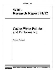
c author’s version, not for redistribution, IEEE Nehalem Quadcore
Nehalem Quadcore
Core 0 Core 1 Core 2 Core 3
Core 4 Core 5 Core 6 Core 7
L1
L1
L1
L1
L1
L1
L1
L1
L2
L2
L2
L2
L2
L2
L2
L2
QPI
I/O Hub
Figure 1.
System overview
Although the basic structure of the memory hierarchy is similar for Nehalem and Shanghai based processors, the implementation details differ. While AMD processors use a “non-inclusive” L3 cache, Intel implements an inclusive last level cache. “core valid bits” within the L3 cache indicate that a cache line may be present in a certain core. If a bit is not set, the associated core certainly does not hold a copy of the cache line, thus reducing snoop traffic to that core. However, unmodified cache lines may be evicted from a core’s cache without notification of the L3 cache. Therefore, a set core valid bit does not guarantee the presence of the cache line in a higher level cache. Generally speaking, the shared last level cache with its core valid bits has the potential to strongly improve the performance of on-chip data transfers between cores while filtering most unnecessary snoop traffic. Nehalem is the first microarchitecture that uses the MESIF cache coherency protocol. It extends the MESI protocol used in previous Xeon generations by a fifth state called forwarding. This state allows unmodified data that is shared by two processors to be forwarded to a third one. We therefore expect the MESIF improvements to be limited to systems with more than two processors. The benchmark results of our dual-processor test system configuration should not be influenced.
III. S YSTEM A RCHITECTURE Previous generation quad-core Xeon processors (Harpertown) are composed of two dual-core dies each with a shared L2 cache. In contrast, the Xeon 5500 series processors (Nehalem-EP) are a native quad-core design. Similar to quad-core AMD Opteron processors (Shanghai), the L1 and L2 caches are implemented per core, while the L3 cache is shared among all cores of one processor. The Front Side Bus used in previous Intel CPUs is replaced by point-to-point links called Quick Path Interconnect (QPI). Moreover, each processor contains its own integrated memory controller (IMC). The basic design of a two-socket Nehalem system is depicted in Figure 1. The Intel Nehalem microarchitecture supports simultaneous multithreading (SMT) that allows each core to execute two threads in parallel. This technique is well-known from the Pentium 4 processors based on Intel’s Netburst microarchitecture. Furthermore, processors based on the Nehalem microarchitecture feature a dynamic overclocking mechanism (Intel Turbo Boost Technology) that allows the processor to raise core frequencies as long as the thermal limit is not exceeded. Table I shows the key differences between the Nehalem microarchitecture and other common x86 64 server CPUs.
Table I C OMPARISON OF DIFFERENT X 86 64 MICROARCHITECTURES Processor
AMD Opteron 238*
Intel Xeon 54**
Intel Xeon 55**
Shanghai
Harpertown
Nehalem-EP
non-inclusive
inclusive
inclusive
MOESI
MESI
MESIF
Shared last level cache
yes
no
yes
Integrated memory controller
yes
no
yes
Point-to-point processor interconnect
yes
no
yes
Native quad-core design
yes
no
yes
Microarchitecture Cache organization Cache coherency protocol
IMC (3 Channel)
DDR3 F
QPI
DDR3 C
DDR3 B
DDR3 A
IMC (3 Channel)
Shared Level 3 Cache
DDR3 E
Shared Level 3 Cache
DDR3 D
The Nehalem microarchitecture implements the MESIF cache coherency protocol, an extended version of the wellknown MESI protocol [5, p. 213]. Due to the novelty of this microarchitecture, we can only refer to a very limited number of publications that are relevant for our test system. Some information can be gathered from Intel documents [6], [7]. However, none of them describe the architecture in much detail. We use BenchIT [8] to develop and run our memory benchmarks as well as for the results evaluation. This performance measurement suite is designed to run microbenchmarks on every POSIX 1.003 compliant system in a user-friendly way. It helps to compare different algorithms, implementations of algorithms, properties of the software stack, and hardware details of whole systems. The software is available as Open Source.
c author’s version, not for redistribution, IEEE IV. T EST S YSTEM AND B ENCHMARK D ESIGN The configuration of our test system is detailed in Table II. We disabled dynamic overclocking to exclude potential interference factors. Our benchmarks use only one thread per core. We therefore disabled the SMT feature. The “adjacent line prefetcher” was always enabled in the BIOS of our test system, whereas the “hardware prefetcher” was disabled if not noted otherwise. Table II T EST SYSTEM CONFIGURATION Processors
2x Intel Xeon X5570
Core arrangement
Processor 0: core 0-3 Processor 1: core 4-7
Core frequency
2.933 GHz
Uncore frequency
2.666 GHz
QPI bandwidth
25.6 GB/s per link
L1 cache size
32 KiB/32 KiB
L2 cache size
256 KiB
L3 cache size
8 MiB
Cache line size Page size L1 data TLB L2 TLB Memory type Operating System Compiler
64 Bytes 4 KiB/2 MiB (small/huge pages) 48/32 entries for small/huge pages 512 entries for small pages 6x 2 GiB DDR3-1333, registered, ECC 3 channels per processor, 10.66 GB/s each Debian 5.0, Kernel 2.6.28.1 gcc 4.3.2 and icc 11.0
We used two kinds of benchmarks to measure the performance of the memory subsystem. Hand optimized assembler benchmarks (see Section IV-A) are used to determine minimal read latency and the maximal read and write bandwidth. Additionally, a modified version of the STREAM [4] benchmark (see Section IV-B) is used to verify the results from the assembler benchmarks and examine more complex memory access patterns. The benchmarks are available as Open Source on the BenchIT website (www.benchit.org). A. Assembler Benchmarks Our compiler independent assembler benchmarks are designed to run on 64 Bit x86 processors (Intel and AMD). They use instruction sequences that can not be generated using C, e.g. transfer data into registers without computing on it. Only the measurement routine itself is programmed in assembler, the rest (e.g. memory allocation) is written in C. Our timer is the high resolution Time Stamp Counter. However, a small overhead exists that is noticeable especially in the L1 results. Each thread of the benchmark program is pinned to a certain core. In the following description, thread N will always run on core N. We ensure that all memory pages of each thread are physically allocated in the corresponding memory DIMMs, allowing us to reveal effects caused by the NUMA architecture.
Prior to the measurement, data is placed in the caches in a certain coherency state. These states are generated as follows: • Modified state in caches of core N is generated by: Thread N writing the data, which also invalidates all copies that may exist in other cores. • Exclusive state in caches of core N is generated by: 1) Thread N writing to the memory to invalidate copies in other caches, 2) Thread N invalidating its cache using the clflush instruction, 3) Thread N reading the data • Shared state in caches of core N is generated by: 1) Thread N caching data in exclusive state, 2) Reading the data from another core Memory benchmarks and especially latency measurements often show a mixture of effects from different cache levels rather than just one. If appropriate, we use a special cache flush routine to explicitly measure the performance of a certain cache level. If the dataset used for the measurement does not fit into a certain cache level, the cache flush routine completely replaces the data in this (and higher) cache levels with dummy data that is not accessed during the measurement. Translation lookaside buffer (TLB) misses are another effect that can strongly influence the results of memory benchmarks. We use “huge pages” to prevent TLB misses up to a dataset size of 64 MiB of contiguous memory. The dummy data for our cache flushes is allocated using small pages. The Nehalem microarchitecture implements separated TLB entries for small and huge pages. Therefore, the cache flushes do not affect the TLB entries needed for the measurement. The latency benchmark (see Section V) uses pointerchasing to determine the latency for accesses to main memory and different cache levels (local and other cores), respectively. The following implementation model describes a latency measurement of core 0 accessing memory associated with core N: 1) 2) 3) 4) 5) 6)
thread 0: warm-up TLB if (N>0): sync of thread 0 and N thread N: access data (-> E/M/S) if (N>0): sync of thread 0 and N all threads: flush caches (optional) thread 0: measure latency
Step 1 ensures that TLB entries needed for the measurement are always present in core 0. Step 3 places data in the caches of core N in one of the coherency states described earlier. Step 5 optionally performs the cache flush routine described earlier. Step 6 is the final latency measurement and always runs on core 0. The number of accesses during the latency measurement is constant, the access pattern is pseudo-random. Every cache line is accessed only once to avoid reuse of cache lines. No consecutive cache lines are accessed to eliminate the influence of the adjacent line prefetcher.
c author’s version, not for redistribution, IEEE The single-core bandwidth benchmark (see Section VI-A) has a similar structure as the latency benchmark and performs steps 1 to 5 identically. We again control the coherency state of the accessed cache lines to unveil how the coherency protocol affects the memory performance. Moreover, the measurement routine can access different locations of the memory subsystem, including other cores’ caches. We are therefore able to determine local, inter-core, and inter-processor bandwidths. The measurement routine that runs on core 0 (step 6) differs from the latency benchmark. It consecutively accesses a variable amount of data to determine the read or write bandwidth that is available for a single core. We solely use transport instructions to load (MOVDQA) or store (MOVDQA, MOVNTDQ) data in order to avoid being limited by arithmetic operations. With respect to the write bandwidth, it is important to note that current x86 64 microarchitectures do not allow one core to write explicitly into another core’s cache. Therefore, the results of this benchmark are always a combination of two effects: first, the read-for-ownership that is performed prior to the write, and second, the write access to the local cache. This has to be considered in the interpretation of the results. The multicore bandwidth benchmark (see Section VI-B) uses multiple threads concurrently to determine the aggregate bandwidth for a variable number of cores. This is particularly helpful to determine the characteristics of the shared L3 cache and the integrated memory controller for simultaneous accesses of multiple cores. The memory access routine is similar to the previous benchmark and consecutively accesses a variable amount of data that is privately allocated by each thread. For this benchmark it is very important that all parallel threads are tightly synchronized. We use the Time Stamp Counter (TSC) for this purpose. This requires system-wide synchronous TSCs, which is the case in our test system. All cores increment the TSC at a constant rate set to a fixed multiple of an external reference clock. The latter is received from an external clock source jointly used by both processors. To ensure that all accesses occur between two timestamps, we use the minimal start time and maximal end time of all threads to calculate the accumulated bandwidth. The implementation model of the benchmark looks as follows: 1) 2) 3) 4) 5) 6) 7) 8) 9)
all threads: access data (-> E/M) all threads: flush caches (optional) all threads: barrier synchronization thread 0: define start_time in future all threads: wait for start_time all threads: measure t_begin all threads: access data (read/write) all threads: measure t_end duration = max(t_end) - min(t_begin)
B. Modified STREAM Benchmarks The last benchmark presented in this paper resembles STREAM, a well-know and frequently used set of bandwidth benchmarks [4]. We mainly use it to crosscheck the results of our assembler routines and find potential weaknesses of either the C or the assembler implementation. Additionally, it is used to investigate the performance of more complex memory access patterns that involve reads and writes. The original STREAM benchmark uses four different memory access patterns which implement calculations on one-dimensional arrays of double precision floating point numbers. The second version, called STREAM2, also defined memory accesses for read-only and write-only operations. Our C benchmarks are comparable to STREAM(2) as they use the same access patterns. However, there are several differences compared to the original version: • Every OpenMP thread is bound to a specific core and allocates its own memory. • Time measurement uses the Time Stamp Counter and is done within the parallel region to remove thread creation overhead from the measurement. • The best results of multiple runs are chosen to reduce interferences. • Use of vector pragmas to improve compiler optimizations: #pragma vector aligned for fast aligned memory access, #pragma vector nontemporal for explicit write-back of data to main memory without polluting the caches. The Intel C++ Compiler 11.0 (-O3) was used to generate optimal code for the underlying architecture and maximize the performance. V. L ATENCY R ESULTS In this Section we present the results of our latency measurements on the Intel Nehalem test system. We determine the latency for accesses to cache lines in variable coherency states that are placed in different locations of the memory subsystem. The benchmark implementation is detailed in Section IV. The results for exclusive and modified cache lines are presented in Figure 2. Table III summarizes these results and additionally includes results for shared cache lines. A variety of conclusions can be drawn from these results and we describe most of them below. The latencies to local caches are independent of the coherency state since the data can be read directly in all states. In agreement with [6] we measure a latency of 4 and 10 cycles for the L1 and L2 cache, respectively. The L3 cache latency (38 cycles) is 3 cycles higher than Intel specifies for processors with identical core and uncore frequency, likely caused by the differing clock speeds in our test system.
c author’s version, not for redistribution, IEEE
(a) Exclusive cache lines
Figure 2.
(b) Modified cache lines
Read latencies of core 0 accessing cache lines of core 0 (local), core 1 (on die) or core 4 (via QPI)
The latencies to other cores on the same processor strongly depend on the cache line’s coherency state. The latency for unmodified cache lines in other cores is independent of the cache level since the inclusive L3 cache can answer all requests. Shared cache lines (two or more core valid bits set) can be accessed within 13 ns. The L3 cache contains a valid copy and will immediately respond to a request without snooping other cores. In contrast, exclusive cache lines (one core valid bit set) may have been modified in a higher level cache, forcing the L3 cache to check the coherency state in the core. This snoop results in a 9.2 ns penalty that increases the latency to 22.2 ns. Due to the silent eviction from higher level caches, this penalty even occurs for cache lines only present in the L3 cache. For requests to modified cache lines (see Figure 2b), the data has to be gathered from the cache that contains the latest copy. The eviction of modified cache lines from a higher level requires a write-back to the L3 cache that will also update the core valid bits. Therefore, the L3 cache can deliver these cache lines with the lowest latency (13 ns). Data that are still present in higher cache levels (indicated by the core valid bit) are requested from the L2 or L1 cache, thus resulting in a higher latency (25.5 or 28.3 ns). Evidently the shared L3 cache serves as the central and single unit for on-chip inter-core data transfers.
The latencies to the other processor include an additional penalty for the data transfer via QPI. For exclusive cache lines the whole access includes a snoop of one core in the other processor and requires 63 ns. This is a penalty of 41 ns compared to the local access (22.2 ns). The latency for shared cache lines is slightly lower (58 ns). Again, the L3 cache can directly answer request for shared cache lines. However, the QPI penalty of 45 ns compared to the local access (13 ns) is 4 ns higher than for exclusive cache lines. The latency for modified cache lines exceeds 100 ns. This occurs due to write-backs to main memory that are required by the cache coherency protocol. The latency to main memory is 65 ns for local accesses. The QPI penalty of 41 ns increases the total latency to 106 ns when remote memory is accessed. A slowly increasing latency for memory sizes that exceed 64 MiB shows the effect of insufficient L1 data TLB entries. In general, the main memory latency is: lram = lL3miss (+lQP I ) + lIM C/DIM M . The absolute values strongly depend on the actual test system, e.g. the processor’s core and uncore frequency. In our case, the formula looks as follows: lram = 13ns (+41ns) + 52ns.
Table III R EAD LATENCIES OF CORE 0, ALL RESULTS IN NANOSECONDS ( CYCLES ) Exclusive cache lines L2 L3
Source
L1
Local Core1 (on die)
1.3 (4)
Core4 (QPI)
3.4 (10) 13.0 (38) 22.2 (65) 63.4 (186)
L1
Modified cache lines L2 L3
1.3 (4) 28.3 (83)
3.4 (10) 25.5 (75) 102 - 109
13.0 (38)
L1
Shared cache lines L2 L3
1.3 (4)
RAM
3.4 (10) 13.0 (38) 13.0 (38)
65.1
58.0 (170)
106.0
c author’s version, not for redistribution, IEEE
(a) Exclusive cache lines
Figure 3.
(b) Modified cache lines
Read bandwidth of core 0 accessing cache lines of core 0 (local), core 1 (on die) or core 4 (via QPI)
VI. BANDWIDTH R ESULTS
The results of our single-core bandwidth benchmarks show the available transfer rate when accessing data located
in certain cache levels of different cores. Section VI-B discusses the main memory in more detail. We use our designated cache flush routines (see Section IV) to ensure that data is fetched or written back solely to the intended cache level or main memory. In Figure 3 we plot the read bandwidth over the memory size for both exclusive and modified cache lines. Table IV summarizes the data. The results for write bandwidths are presented in Figure 4 and Table V. The bandwidth to local caches is independent from the coherency state of the accessed data. This is consistent with our latency results. We measure an L1 bandwidth of 45.6 GB/s, nearly reaching theoretical peak performance. Read and write bandwidth for L2 cache (31.1/28.8 GB/s) and L3 cache (26.2/19.9 GB/s) cannot be derived from the available documentation. We conclude that the non-optimal bandwidths of lower cache levels mainly originate from conflicts caused by simultaneous L1 accesses (Core accesses L1, transfers between L1 and other caches/memory). The write bandwidth is lower than the read bandwidth as data is actually read before it can be written, effectively doubling the amount of transferred data. However, the write performance only suffers a minor penalty, especially in the L2 cache. The 256 bit interfaces of both the L2 and L3 cache clearly pay off and prevent larger write penalties.
Table IV C ORE 0 READ BANDWIDTH IN GB/ S
Table V C ORE 0 WRITE BANDWIDTH IN GB/ S
Each core of an Intel Nehalem processor has one 128 bit write port and one 128 bit read port [6] to the L1 cache. At a core clock rate of 2.933 GHz, this limits the available L1 bandwidth to 46.9 GB/s per direction (read/write). The L2 caches have 256 bit interfaces used for both reading and writing, as has the L3 cache. However, the latter is shared between all four cores of one processor. All cache lines accessed by a core are placed in its L1 cache. Moreover, the Nehalem microarchitecture implements a write-allocate cache policy (except for non-temporal stores [6]). Any write access to a cache line that is not present in a local cache triggers a read for ownership before actually writing the cache line. Main memory is the lowest level of the memory subsystem that we analyze with our benchmarks. Each triplechannel integrated memory controller (IMC) has a theoretical peak bandwidth of 32 GB/s when equipped with DDR31333 DIMMs. The following Sections demonstrate the single- and multicore bandwidths that can be achieved practically. A. Single-core Bandwidth
L1
Exclusive L2 L3
Local Core1
45.6 19.3
31.1 26.2 19.7
Core4
9.0
9.2
L1 45.6 9.4
Modified L2 L3 31.1 13.2 5.6
26.2
RAM
L1
10.1
Local Core1
6.3
Core4
45.6 23.4
Exclusive L2 L3 28.8 22.2 9.0
19.9 17.6
L1
Modified L2 L3
45.6 9.4
28.8 13.0 8.3
RAM
19.9
8.4
9.6
5.5
c author’s version, not for redistribution, IEEE
(a) Exclusive cache lines
Figure 4.
(b) Modified cache lines
Write bandwidth of core 0 accessing cache lines of core 0 (local), core 1 (on die) or core 4 (via QPI)
The bandwidth to other cores on the same processor strongly depends on the coherency state of the accessed data. Reading and writing modified data in the L3 cache again achieves 26.2 GB/s or 19.9 GB/s, respectively. If the latest copy is in the local caches of the remote core, read bandwidth decreases to 13.2 GB/s in the L2 and 9.4 GB/s in the L1 cache. This picture fully corresponds with our latency results (see Figure 2b). The L1 and L2 write bandwidth results resemble the corresponding read bandwidths. The limiting factor for this case is the read for ownership of the remote cache lines rather than writing to the local caches. Read accesses to exclusive cache lines can be served by the inclusive L3 cache. However, the L3 cache is not aware whether the data has been modified in the higher cache levels or not. The snooping overhead limits the bandwidth to 19.7 GB/s for all cache levels, including the L3 cache. The latter is an effect of the silent eviction from higher level caches and again very much in accordance with our latency results. Write accesses to exclusive cache lines from another core of the same processor achieve 23.4 and 22.2 GB/s for the L1 and L2 cache respectively. This means that the write bandwidth for L1/L2 data is actually higher than the corresponding read bandwidth. This effect is surprising and difficult to explain with the available documentation. However, the difference is not large. The bandwidth to the other processor is mainly limited by the Quick Path Interconnect. Our benchmarks could not achieve its theoretical peak bandwidth of 12.8 GB/s per direction. We measure about 9 GB/s for reading and writing exclusive cache lines. The bandwidth for writing data modified by a core of the second processor is very similar. However, the bandwidth significantly decreases to 5.6 GB/s when reading modified cache lines. In this case,
data is written back to main memory as required by the coherency protocol for cache lines that are shared between both processors. In contrast, write accesses to modified cache lines do not require writing back data as the cache lines remain in a modified state. Therefore, higher bandwidths can be achieved. The bandwidth with enabled prefetcher reflects the performance of the default processor configuration. Table VI summarizes our results. The absolute bandwidth difference compared to the case with disabled prefetcher is listed as second value in each cell (+/- refers to a bandwidth improvement/degradation due to the activation of the prefetcher). The prefetcher improves the bandwidth in most cases. Only the L3 performance slightly drops by 2.7 GB/s in some situations. It is interesting to note that this only occurs in cases where the L3 cache bandwidth with deactivated prefetcher is at its limit of 26.2 GB/s. In contrast, the prefetcher is beneficial if snoops of other cores limit the L3 bandwidth. The main memory bandwidth and the bandwidth to the second processor via QPI improve significantly when prefetchers are enabled. Table VI C ORE 0 READ BANDWIDTHS WITH PREFETCHER ( IN GB/ S ) AND DIFFERENCE COMPARED TO RESULTS WITHOUT PREFETCHER ( IN GB/ S )
L1
Exclusive L2 L3
L1
Modified L2 L3
RAM
Local
45.6 ±0
31.1 ±0
23.5 -2.7
45.6 ±0
31.1 ±0
23.5 -2.7
13.8 +3.7
Core1
22.5 +3.2
23.8 +3.1
23.8 +3.1
9.4 ±0
13.2 ±0
23.5 -2.7
13.8 +3.7
Core4
9.6 +0.6
10.0 +0.8
10.0 +0.8
8.1 +2.5
8.1 +2.5
8.5 +2.9
9.0 +2.7
c author’s version, not for redistribution, IEEE
(a) Exclusive cache lines
Figure 5.
(b) Modified cache lines
Accumulated read bandwidth using multiple threads
B. Multicore Bandwidth In this Section we discuss the available bandwidth when multiple cores access memory concurrently. This test is primarily targeted at the shared L3 cache and the integrated memory controller. All threads work on disjoint data, assuring that data streams are independent from each other. Cache flushes have not been used as they hide interesting effects. The results for read and write bandwidth are depicted in Figure 5 and 6, respectively. Any access to a cache line that is not present in the L1 cache causes its transfer into this cache. Consequently, the eviction of older cache lines is required. This occurs silently for exclusive cache lines, while the write-back of modified lines requires additional bandwidth. The read bandwidth for exclusive cache lines as depicted in Figure 5a allows to estimate the performance for concurrent read accesses to certain cache levels. In contrast, reading modified data is influenced by additional write-backs, especially for data sizes that exceed the local caches (see Figure 5b). For exclusive cache lines, the silent evictions prevent selective writes to certain cache levels. For example, writing 64 KiB results in writing 32 KiB into L1 and 32 KiB into L2 cache. Write bandwidths to modified data are more comprehensible. Writing 64 KiB results in writing 64 KiB into L2 cache, 32 KiB of new data and 32 KiB of evicted older data. As expected, the bandwidth of the L1 and L2 caches scale well with the number of cores used. Therefore, the rest of this Section concentrates on the L3 cache and the main memory. Our intention is to determine bandwidths of the individual cache levels. Therefore, reading exclusive cache lines and writing to modified lines are the most interesting cases for us. The results are summarized in Table VII, which also includes the bandwidth of non-temporal stores.
The L3 bandwidth for reading exclusive cache lines only scales well for up to three cores with 26 GB/s each as depicted in in Figure 5a. The performance with four cores is limited to 85.3 GB/s by the L3 cache (2.66 GHz, 32 Bytes per cycle). In contrast, the bandwidth for multiple cores writing to the L3 cache (as depicted in Figure 6b) scales weakly. Two cores can saturate the L3 write bandwidth. The read bandwidth of modified data (see Figure 5b) reveals a potential bottleneck. In this case, all cores writeback their modified L1 and L2 cache content concurrently while reading from the L3 cache. Therefore, the L3 write bandwidth limits the L3 read bandwidth in this situation. The read performance increases with growing data sets. This can be explained with the growing amount of read data, whereas the number of write-backs is determined by the size of the higher level caches and therefore constant. The memory bandwidth of a single reading core is limited by the number of transactions in flight. The theoretical maximum can be estimated using Littles Law [9]: bandwidth =
Bytes/T rans. ∗ T rans. in f light latency
Table VII L3 AND MAIN MEMORY BANDWIDTH IN GB/ S L3 Cache
RAM non-temporal write w/o pref. w/ pref.
Cores (Sockets)
read
write
read
1 (1)
26.2
19.9
10.1
8.4
8.5
8.5
2 (1)
52.2
27.2
19.3
12.0
12.3
10.7
3 (1)
77.3
26.5
22.7
12.0
13
11.5
4 (1)
85.0
26.0
23.0
12.0
14.1
11.5
8 (2)
170.0
52.0
41.9
22.3
28.2
23.2
write
c author’s version, not for redistribution, IEEE
(a) Exclusive cache lines
Figure 6.
(b) Modified cache lines
Accumulated write bandwidth using multiple threads
In our case, a single core’s fill buffers [6] allow a maximum of 10 concurrent memory requests of 64 Bytes each (cache line size). With a latency of 61.7 ns (memory latency minus L2 cache latency), the peak bandwidth calculates as follows: 64 Bytes ∗ 10 = 10.4 GB/s bandwidth = 61.7 ns Our measurement result of 10.1 GB/s is only slightly below the theoretical peak. The bandwidth scales well when using two cores. However, only minor improvements can be achieved with three and four cores. The maximum of 23 GB/s does not meet the expectations. Considering the three channel memory interface with a bandwidth of 10.6 GB/s per channel, a theoretical peak bandwidth of 32 GB/s can be expected. It is interesting to note that we achieve a bandwidth of 10.1 GB/s when only one memory channel is populated. Two channels scale well, as a bandwidth of 19 GB/s can be achieved. The write bandwidth to main memory is limited to 12 GB/s per processor and can be reached using two cores. This is significantly slower than the read bandwidth but can be explained with the write-allocate mechanism: data needs to be read before writing, effectively doubling the required bandwidth. Non-temporal stores slightly improve the write bandwidth unless the hardware prefetcher is enabled.
Compared to our assembler results, read bandwidths (DDOT) tend to be slightly lower in all levels of the memory subsystem. Generally the bandwidths are similar to our assembler results with enabled hardware prefetchers. The highest deviation is measured for the L2 cache, presumably due to memory access patterns of DDOT that cause more conflicts than our assembler routine. The results for writing (Fill) almost perfectly match the assembler results for all three cache levels. The main memory bandwidth is close to the assembler result using non-temporal stores, which are generated by the used Intel C++ compiler (11.0) as well. For Triad and Copy, the L1 bandwidth exceeds those for solely reading or writing. In case of Copy, read and write accesses can be done in parallel, effectively doubling the achievable bandwidth. The Triad bandwidth can be explained with a read/write-ratio of 2:1 that prevents the use of half of the available write bandwidth. The results for the L2 cache slightly improve as well. However, the 256 bit interfaces are not fully utilized. Table VIII STREAM(2) BANDWIDTH IN GB/ S Kernel
Threads
L1
L2
L3
RAM
Triad
1 4
67.71 270.01
34.6 134.4
24.0 50.9
12.72 19.02
Copy
1 4
89.2 353.7
35.8 143.6
23.8 41.1
11.21 18.81
Fill
1 4
45.2 168.8
28.8 113.9
20.3 25.7
8.52 13.92
DDOT
1 4
45.2 168.2
27.8 109.7
23.01 79.3
13.31 20.81
C. Modified STREAM Benchmarks This Section discusses the results of our STREAM derived benchmarks, mainly used to verify our assembler benchmarks and investigate properties of alternating reads and writes (Copy, Triad). The STREAM bandwidths are strongly influenced by the use of non-temporal stores and the prefetcher settings. Only the best results of several configurations are presented in Table VIII.
1 prefetcher 2 using
enabled #pragma vector nontemporal
c author’s version, not for redistribution, IEEE VII. C ONCLUSIONS AND F UTURE W ORK Understanding the properties and performance of the hierarchical memory system of today’s computers is a key factor to obtain good application performance. In this work we have presented a new set of latency and bandwidth benchmarks for multicore x86 64 architectures. Two major novelties characterize our approach: First, the explicit control of the data’s cache coherency state. Second, the welldefined data placement in every available cache and memory location of a multi-core and multi-processor ccNUMA system. Our benchmark software is publicly available as Open Source. We have demonstrated the potential of our approach with a detailed analysis of the memory hierarchy of a two socket, quad-core Intel Nehalem test system. The Nehalem microarchitecture features an integrated memory controller, an extended cache coherency protocol and a ccNUMA architecture. Our results reveal a fast and well-designed memory subsystem. It performs particularly well in most scenarios that involve on-chip cache-to-cache data transfers. However, we have also disclosed some potential bottlenecks. The L1 and L2 caches are implemented per core and we find the multicore cache bandwidth to scale accordingly. The L3 bandwidth is shared, scaling well up to three cores for simultaneous accesses. With concurrent accesses from all four cores, the per-core read bandwidth decreases from 26 GB/s to about 21 GB/s. The accumulated bandwidth of 85 GB/s currently forms no major limitation, though it will hopefully be improved for future eight-core implementations. On the contrary, the write performance of the L3 cache is more limited. An aggregated bandwidth of about 27 GB/s is available for all four cores. This can also reduce the read bandwidth if modified cache lines have to be written back from the core’s local caches. Our observations indicate that the shared L3 cache performs well as the central connection between all cores of one processor. Most unnecessary core snoops are filtered. Requests to shared cache lines are not forwarded to the cores. For modified cache lines, requests are only forwarded to one core or handled by the L3 if the core already evicted the data. Only request to exclusive cache lines always have to be forwarded to one core, which is the trade-off for silent eviction. We have not been able to fully utilize all three memory channels of our test system. This may be an architectural limit or a problem of our test hardware. Apart from that, a main memory bandwidth of 23 GB/s per processor is significantly higher than for any other x86 system to date. However, single cores can not fully utilize this bandwidth. With respect to the QPI point-to-point interconnect, our benchmarks show that a bandwidth of up to 10 GB/s can be achieved per direction. This limits the inter-processor memory bandwidth for both cache and main memory accesses.
A detailed comparison with other cache coherency protocols and architectures is beyond the scope of this paper and subject to future work. We have disclosed some effects of the hardware prefetchers that for example decrease the throughput of non-temporal stores and need to be investigated further. Our benchmarks are perfectly suitable to analyze the ccNUMA implementation of large, Nehalem-EX based shared memory systems. In addition we will study future multi- and many-core microarchitectures that are likely to implement even more complex cache architectures. We also plan to incorporate performance counters into our benchmarks in order to identify indicators for bad performance. This may allow the correlation of performance anomalies in applications to properties of the underlying hardware. ACKNOWLEDGMENT This work was funded in part by the BMBF grant 01IS07005B within the ParMA (Parallel Programming for Multi-core Architectures) project. In addition, this work substantially benefited from the early availability of an Intel Nehalem evaluation platform. The authors would like to thank Intel Germany for providing these resources. R EFERENCES [1] V. Babka and P. T˚uma, “Investigating cache parameters of x86 family processors,” in SPEC Benchmark Workshop, 2009, pp. 77–96. [2] L. Peng, J.-K. Peir, T. K. Prakash, C. Staelin, Y.-K. Chen, and D. Koppelman, “Memory hierarchy performance measurement of commercial dual-core desktop processors,” Journal of Systems Architecture, vol. 54, no. 8, pp. 816 – 828, 2008. [3] J. D. McCalpin, “Stream: Sustainable memory bandwidth in high performance computers,” University of Virginia, Tech. Rep., 1991-2007. [Online]. Available: http://www.cs.virginia. edu/stream/ [4] J. D. McCalpin, “Memory bandwidth and machine balance in current high performance computers,” IEEE Computer Society Technical Committee on Computer Architecture (TCCA) Newsletter, pp. 19–25, December 1995. [5] J. L. Hennessy and D. A. Patterson, Computer Architecture: A Quantitative Approach, 4th ed. Morgan Kaufmann Publishers, 2006. [6] Intel 64 and IA-32 Architectures Optimization Reference Manual, Intel, December 2008. [Online]. Available: http: //developer.intel.com/products/processor/manuals/ [7] An Introduction to the Intel QuickPath Interconnect, Intel, January 2009. [Online]. Available: http://www.intel. com/technology/quickpath/introduction.pdf [8] G. Juckeland, M. Kluge, W. E. Nagel, and S. Pfl¨uger, “Performance analysis with BenchIT: Portable, flexible, easy to use,” in Proceedings of the International Conference on Quantitative Evaluation of Systems, 2004, pp. 320–321. [9] J. D. Little, “A proof for the queueing formula: L = λ · W ,” Operations Research, vol. 9, no. 3, 1961.