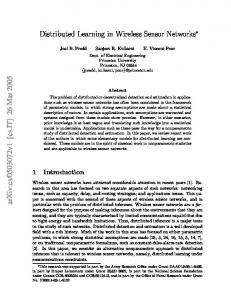
autonomous, wireless sensor nodes (Figure 1) that can be ... The main advantages of this technique .... attractive wireless communications technique for minute.
MEMS for Distributed Wireless Sensor Networks Brett A. Warneke, Kristofer S.J. Pister Berkeley Sensor and Actuator Center, University of California at Berkeley ABSTRACT
Interrogating Laser Beam Laser
MEMS technology is enabling the development of inexpensive, autonomous wireless sensor nodes with volumes ranging from cubic mm to several cubic cm. These tiny sensor nodes can form rapidly deployed, massive distributed networks to allow unobtrusive, spatially dense, sensing and communication. MEMS enable these devices by reducing both the volume and energy consumption of various components. This paper will review some of the wireless sensor nodes under development and applicable MEMS devices for small and efficient optical communication, micropower generation, and sensing. In addition, CMOS post-process micromachining will be discussed as a method of achieving low cost and high integration.
1. INTRODUCTION Over the course of the last several decades, technological advances have promoted exponential decreases in the size of computational functionality, rapid growth in the number of networked devices, escalating numbers of wireless devices, diminishing wireless device sizes, enhanced battery life, brisk reduction in sensor sizes, and a continual decline in cost. The convergence of these trends is expected to result in “ubiquitous computing” [1]. One manifestation of ubiquitous computing will be small, inexpensive, autonomous, wireless sensor nodes (Figure 1) that can be rapidly deployed in vast numbers throughout the environment. Because of the discreet size, substantial functionality, connectivity, and low cost, these devices will enable completely new methods of interacting with the environment, providing more information from more places in a less intrusive way than before. Application areas include defense networks that could be rapidly deployed by unmanned aerial vehicles (UAV), tracking the movements of birds, small animals, and even insects, fingertip accelerometer virtual keyboards, monitoring environmental conditions that affect crops and livestock, inventory control, product quality monitoring, smart office spaces, and interfaces for the disabled. The primary facilitators for the aforementioned trends are advances in microfabrication technology, both in microelectronics and microelectromechanical systems (MEMS). MEMS technology in particular and more recently is allowing a dramatic reduction in the size and power consumption of sensors, actuators, communication components, and power systems. Progress in
Lens
Mirror
Mirrors
Passive Transmitter with Corner-Cube Retroreflector
Sensors
Active Transmitter with Beam Steering
Incoming Laser Communication
Photodetector and Receiver
Analog I/O, DSP, Control
Power Capacitor
Solar Cell Thick-Film Battery 1-2mm
Figure 1: Conceptual Diagram of a Smart Dust mote, one example of a tiny, autonomous, wireless sensor node.
microelectronics is also a major contributor to the realization of tiny wireless sensor nodes by increasing the amount of functionality that can be packed into a given area, by enhancing levels of circuit integration with mixed-signal design, and by reducing circuit power consumption. However, this paper will focus on the contribution of MEMS to wireless sensor nodes. This paper will begin with a description of some microfabrication processes that provide high levels of integration, which is beneficial to building small systems, then discuss the primary components of these nodes: sensors, communication, and micropower sources. Finally, some example sensor systems will be reviewed, with particular emphasis on the authors’ own work on the Smart Dust project, which has achieved a 16 mm3 node.
2. HIGHLY INTEGRATED PROCESSES Shrinking an entire autonomous system into volumes between a cubic mm and a cubic cm can be assisted by utilizing highly integrated processes that allow disparate components to be fabricated on a common substrate. Frequently, such a process would combine CMOS transistors with some micromachining capabilities. One approach to this that has been successfully commercialized by Analog Devices [2] begins with a standard BiCMOS process, then a 4µm low-stress polysilicon structural layer is inserted into the process before the interconnect metalization is deposited. An extra mask at the end protects the oxide over the circuits during the sacrificial oxide release etch. A similar approach developed by Sandia National Laboratory [3] forms the microstructures before the CMOS by fabricating the polysilicon structures in a trench in the
different process. These die are presently hand-assembled, but production would utilize microassembly techniques. Additionally, the next generation device will pack the same functionality into two die: a CMOS ASIC and a highly integrated custom process that yields solar cells, high voltage FETs, and micromachined structures. Figure 2: Cross-sectional diagram of an etch hole in a standard CMOS process that has been post-processed with an isotropic etchant. Contact, via, and overglass cut layers are stacked to yield the oxide hole to the substrate.
silicon substrate. The trench is refilled with sacrificial oxide then the CMOS process is run. The main advantages of this technique are that the CMOS process does not need substantial modification and its thermal budget is unaffected by the polysilicon deposition. Despite being based on standard CMOS, both of these integrated processes require control over the fabrication flow to add the micromechanical layers. A number of approaches have been developed to do post-process micromachining on foundry CMOS. Franke, et al. [4] demonstrated post-CMOS modular integration of poly-SiGe microstructures with polyGe sacrificial layers. LPCVD poly-Ge and poly-SiGe can be deposited at such a low temperature that the CMOS aluminum interconnects are not damaged. Furthermore, hydrogen peroxide etches poly-Ge without attacking the CMOS layers, which simplifies the process. An even simpler method allows micromachining to be performed with a single maskless post-processing step [5] on foundry CMOS wafers or die, thus requiring very little extra equipment. This technique relies on the ability to stack the contact, via, and overglass cut layers (Figure 2) to yield a ‘pit’ of exposed silicon when the chip returns from the foundry, which can then be sacrificially etched by bulk Si etchants such as xenon difluoride (XeF2) [6], tetramethylammonium hydroxide (TMAH), and ethylenediamine-pyrocatechol (EDP) [7] with the oxide acting as the mask and structural layer. Each of these etch methods require relatively inexpensive equipment and infrastructure, making this a viable option for designers without a fabrication facility. This technique has been used to create a wide variety of devices including accelerometers [8], microwave power sensors [7], higher-Q spiral inductors [9], heart-cell transducers [10], thermal sensors [11], and thermally isolated circuits [12]. Although this method does not work in sub-micron processes that use tungsten plugs in the vias, it is still useful in the older, less expensive processes. Another maskless post-CMOS process that does work in sub-micron processes uses the top metal layer as the mask [13]. A high aspect ratio reactive ion etch (RIE) removes the oxide not protected by metal, leaving near vertical sidewalls. Next, a plasma etch removes the silicon substrate from beneath the microstructures. This approach has the advantage of providing high-aspect ratio structures, but it requires expensive processing equipment. An additional technology area that can help shrink an autonomous system is microassembly [14]. Pick and place methods for the microdomain, microtweezers [15], batch transfer, fluidic microassembly, flip-chip bonding, and many other techniques are facilitating the compact assembly of heterogeneous dies. For instance, the current Smart Dust mote, shown in Figure 3, contains four die, each from a
3. SENSORS Standard integrated circuit processes can inherently sense a few phenomenon, such as light and temperature, in a compact area, but micromachining has allowed researchers to shrink many types of sensors into small volumes while often maintaining similar, or even exceeding, performance levels of conventional transducers [16],[17]. Examples include thermal sensors [11], accelerometers [18], gyroscopes [2], pressure sensors [19], microphones [20], radiation detectors, magnetic sensors, flow sensors, and chemical and biological sensors. Several factors need to be considered when selecting sensors for use in tiny wireless sensor nodes: volume; power consumption; suitableness to power cycling, as this is a primary means of reducing the energy consumption, but some sensors require more time to generate a stable measurement than they would be powered off; fabrication and assembly compatibility with other components of the system; and packaging needs, as sensors that require contact with the environment, such as chemicals, add significant packaging considerations.
4. COMMUNICATION Certainly, the most common form of wireless communication in use today is RF/microwave/millimeter wave radiation. While developments in MEMS [21] are reducing the size of RF components and allowing tighter circuit integration, there are certain limitations that make it less efficient in tiny, energy-constrained devices. First, antennas need to be a significant fraction of a wavelength to be at all efficient, so at RF frequencies antennas are relatively long. A second issue is that a small RF antenna will have very low antenna gain, as beam divergence is fundamentally limited by diffraction, which is dependent on wavelength. To achieve the same milliradian collimation of an inexpensive laser pointer at 1GHz would require a 100m antenna. A third problem with RF communication is that the transceivers have poor overall efficiency because there is usually 1-100mW of overhead due to the mixers, biasing, etc.; however, researchers are working to improve these efficiencies and build 100µW radios [22]. A fourth disadvantage of RF communication is that the received power is ∝ 1/d2→7 due to multi-path fading. For groundbased communication, such as mobile telephone, the average factor is four. These reasons combine to make RF communication unattractive for tiny wireless nodes. For example, the Bluetooth radio standard, which was designed for relatively low power consumption devices, costs about 100nJ/bit to communicate over 10s of meters. Nevertheless, since RF radiation can propagate through a wide variety of materials, thus not requiring line-of-sight, wireless nodes designed for certain applications will utilize it. One notable point of correspondence between RF MEMS components, particularly resonators, and tiny wireless nodes is that these
Solar Cell Array
CCR
XL CMOS IC
Figure 3: 16mm3 mock-up of the current Smart Dust system, showing a 0.25µm CMOS ASIC, solar power array, accelerometer and CCR, each on separate die. The functional device does not have the accelerometer.
components often have relatively low power handling capabilities that render them unsuitable for many RF applications; however, these limits are high enough to be applicable to distributed wireless sensor networks that utilize short-range, multi-hop communication links. Free-space optical communication provides an attractive wireless communications technique for minute sensor nodes (Figure 3). First, optical radiators such as laser diodes and mirrors can be made extremely small – 0.03µm3 lasers have been demonstrated [23]. As mentioned above, optical communication also provides extremely high antenna gain, which yields higher transmission efficiencies. Thirdly, while laser output slope efficiencies are only about 25%, the overhead (diode turn-on current) can be as low as 1µW for vertical cavity surface emitting lasers (VCSELs), so the overall output efficiency can be much higher than RF power amplifiers. A fourth advantage of optical communication is that the received power only decays as the inverse of distance squared, assuming line-of-sight communication. Finally, optical communication enables the use of spatial division multiple access (SDMA) [24]. This is a simple technique wherein an imaging receiver can separately process simultaneous transmissions from different angles. As such, SDMA requires no communication overhead and thus has the potential to be more energy-efficient than the RF media access methods such as frequency, time, and code division multiple access (FDMA, TDMA, CDMA). We have explored two approaches to free-space optical transmission: passive reflective systems and active-steered laser systems. The passive reflective system consists of three mutually orthogonal mirrors that form the corner of a cube (Figure 4), hence the name corner cube retroreflector (CCR). Light entering the CCR bounces off each of the mirrors and is reflected back parallel to the incident beam. By electrostatically actuating the bottom mirror, the orthogonality can be broken, causing less light to return to the sender. The CCR can thus communicate with an interrogator by modulating the reflected light, with the only energy consumption being the charging of about 3pF in the actuator and a demonstrated range of 180m [25]. This technique consumes much less power than an approach that
requires the generation of radiation, such as lasers or RF, but it does not facilitate peer-to-peer communication. In such a network the nodes are unlikely to talk to each other, although distributed compression algorithms are being developed to take advantage of such a network. Because a single base-station will simultaneously communicate with potentially thousands of devices, synchronous communication can be used to lock the data sent by each node to a master clock signal from the interrogator. Active-steered laser communication is currently under development. It would utilize an onboard light source, such as a VCSEL, a collimating lens, and MEMS beam-steering optics [26],[27] to send a tightly collimated light beam toward an intended receiver, thus facilitating peer-to-peer communication.
5. MICROPOWER SOURCES Wireless sensor nodes will likely utilize a combination of energy storage and energy scavenging devices. A number of micromachined microbatteries have been reported [28], including some that achieve an energy density of 5.6 J/mm3 [29], which is very competitive with macro-scale batteries. Scavenging energy from the environment will allow the wireless sensor nodes to operate nearly indefinitely, without their battery dying. Solar radiation is the most abundant energy source and yields around 1 mW/mm2 (1 J/day/mm2) in full sunlight or 1 µW/mm2 under bright indoor illumination. Solar cells have conversion efficiencies up to 30% and are a well-established technology, making them attractive for early use in sensor nodes. Vibration harvesting [30] is another potential energy source, scavenging energy from the vibrations of copy machines, ventilation systems, etc. More exotic energy sources include utilizing the excess heat from micro rocket engine [31] combustion and micro radioactive sources.
6. SYSTEMS A number of small, MEMS-based wireless sensor node systems have been developed. Mason, et al. [32] at the University of Michigan built a multisensor microcluster that measures pressure, temperature, humidity, and vibration/position, includes a microcomputer, and has a 50m RF link. The device is less than 10 cm3 and consumes 530µW average power and 10mW while transmitting. Asada, et al. [33] at UCLA developed wireless integrated network sensors (WINS) that included an infrared imager, seismometer, spectrum analyzer, RF transceiver, and lithium coin cells in a volume on the order of tens of cubic inches. Rabaey, et al. [22] at UC Berkeley are researching RF data nodes with less than 5nJ/bit communication energy in a cubic centimeter volume. The authors’ own Smart Dust project [34] seeks to aggressively push the volume of wireless sensor nodes down to a cubic millimeter (Figure 1), which also puts extreme constraints on the energy consumption. The current device [35] is a 16mm3 autonomous solar-powered sensor node with bi-directional optical communication. The device digitizes integrated sensor signals and transmits and receives data optically. The system consists of three die–a 0.25µm CMOS ASIC, a trench-isolation SOI solar cell array, and a
micromachined four-quadrant CCR. The ASIC contains an optical receiver that consumes 69 pJ/bit, an ADC that uses 360 pJ/8-bit sample, a photosensor for measuring ambient light, a finite state machine to control the system, and a 1µW, 3.9MHz integrated oscillator. The CCR consumes about 16 pJ/bit-transmitted. In a new DRIE SOI/CMOS process, we have demonstrated working solar cells, CCRs, and a capacitive accelerometer on a single chip. Once this process is fully developed, the sensor node will shrink to 6.6 mm3. Another forthcoming development is the addition of an ultra-low power custom microprocessor and SRAM to provide greatly enhanced functionality, including laser reprogramming, extreme power cycling, hardware implementation of common tasks for reduced power consumption, and special ADC modes. Assembly and packaging are challenges that remain largely unaddressed.
8. CONCLUSION Technological trends of smaller devices with more functionality, greater connectivity, and more sensors are leading to small, inexpensive, autonomous wireless sensor nodes that will form distributed networks. MEMS are an enabling technology through smaller sensors, communication components, and micropower sources.
9. REFERENCES [1] M. Weiser, et al., “The Coming Age of Calm Technology,” http://www.ubiq.com/hypertext/weiser/acmfuture2endnote.htm, 1996. [2] J.A. Geen, et al., “Single-Chip Surface-Micromachined Integrated Gyroscope with 50º/hour Root Allan Variance,” 2002 IEEE ISSCC., vol.45, San Francisco, Feb. 2002, p. 426-7. [3] J.J. Sniegowski, et al., “IC-Compatible Polysilicon Surface Micromachining,” Annual Rev. Mat. Sci. 2000. 30:299-333. [4] A.E. Franke, et al., “Integrated MEMS technologies,” MRS Bulletin, vol.26, (no.4), Mater. Res. Soc, April 2001, p.291-5. [5] M. Parameswaran, et al., “A new approach for the fabrication of micromechanical structures,” Sensors and Actuators, 19 (1989) 289-307. [6] B. Warneke, K.S.J. Pister, "In situ characterization of CMOS post-process micromachining," Sensors and Actuators A (Physical), Vol. 89, Issue 1-2, 20 March 2001, pp. 142-151. [7] N. Tea, et al., “Hybrid Postprocessing Etching for CMOSCompatible MEMS,” IEEE J. MEMS, 6 (1997) 363-372. [8] E.J.J. Kruglick, B.A. Warneke, and K.S.J. Pister, “CMOS 3axis accelerometers with integrated amplifier,” MEMS 98, Heidelberg, Germany, Jan. 25-29, 1998, pp. 631-636. [9] A. Rofougaran, J. Y.-C. Chang, M. Rofougaran, A.A. Abidi, “A 1 GHz CMOS RF front-end IC for a direct-conversion wireless receiver,” J. Solid State Circuits, 31(1996) 880-889. [10] G. Lin, R.E. Palmer, K.S.J. Pister, and K.P. Roos, “Single heart cell force measured in standard CMOS,” TRANSDUCERS ‘97, Chicago, June 16-19, 1997, p. 199-200. [11] H. Baltes, et al., “Micromachined thermally based CMOS microsensors,” Proc. IEEE, 86 (1998) 1660-1678. [12] E.H. Klaassen, R.J. Reay, C. Storment, and G.T.A. Kovacs, “Micromachined thermally isolated circuits,” Sensors and Actuators A, A58 (1997) pp. 43-50. [13] G.K. Fedder, et al., “Laminated high-aspect-ratio microstructures in a conventional CMOS process,” Sensors and Actuators A (Physical), vol.A57, (no.2), Nov. 1996. p.103-10.
[14] M.B. Cohn, et al., “Microassembly technologies for MEMS,” Proc. SPIE, vol.3511, Micromachining and Microfabrication Process Technology IV, Santa Clara, pp.2-16, 21-22 Sept. 1998. [15] C. Keller, Microfabricated High Aspect Ratio Silicon Flexures, MEMS Precision Instruments, 1998. [16] Lj. Ristic [ed], Sensor Technology and Devices, Artech House, London, 1994. [17] G.T.A. Kovacs, Micromachined Transduceers Sourcebook, WCB McGraw-Hill, San Francisco, 1998. [18] N. Yazdi, F. Ayazi, K. Najafi, “Micromachined inertial sensors,” Proc. IEEE, vol.86, (no.8), Aug. 1998, pp.1640-59. [19] W.P. Eaton, J.H. Smith, “Micromachined pressure sensors: review and recent developments,” Smart Materials and Structures, vol.6, (no.5), Oct. 1997. pp.530-9. [20] P. Rombach, et al., “The first low voltage, low noise differential silicon microphone, technology development and measurement results,” Sensors and Actuators A (Physical), vol.A95, (no.2-3), 1 Jan. 2002, pp.196-201. [21] C.T.-C. Nguyen, L.P.B. Katehi, G.M. Rebeiz, “Micromachined devices for wireless communications,” Proc. IEEE, vol.86, (no.8), Aug. 1998, pp.1756-68. [22] J. Rabaey, et al., "PicoRadios for Wireless Sensor Networks: The Next Challenge in Ultra-Low-Power Design", IEEE ISSCC, San Francisco, Feb. 2002, pp. 200-201. [23] O. Painter, et al., “Two-dimensional photonic band-gap defect mode laser,” Science, vol.284, (no.5421), 11 June 1999, p.1819-21. [24] J.M. Kahn, et al., “Imaging Diversity Receivers for HighSpeed Infrared Wireless Communication,” IEEE Comm., Dec. 1998, pp. 88-94. [25] L. Zhou, K.S.J. Pister, J.M. Kahn, "Assembled Cornercube Retroreflector Quadruplet", MEMS 2002, Las Vegas, Nevada, 20-24 Jan. 2002, p.556-559. [26] M. Last, et al., “An 8 mm3 digitally steered laser beam transmitter,” 2000 IEEE/LEOS Int’l Conf. Optical MEMS, Kauai, HI, p. 69-70. [27] V. Milanovic, M. Last, K.S.J. Pister, ``Torsional Micromirrors with Lateral Actuators,'' Trasducers'01 Eurosensors XV Conference, Muenchen, Germany, Jun. 2001. [28] K.B. Lee, L. Lin, “Electrolyte Based On-Demand and Disposable Microbattery,” MEMS 2002, Las Vegas, Nevada, 20-24 Jan. 2002, p.236-239. [29] W.C. West, et al., “Fabrication and testing of all solid-state microscale lithium batteries for microspacecraft applications,” J. Micromechanics and Microengineering, 12(2002), p. 58-62. [30] S. Meninger, et al., “Vibration-to-electric energy conversion,” IEEE Trans. VLSI Systems, vol.9, (no.1), Feb. 2001, p.64-76. [31] D. Teasdale, V. Milanovic, P. Chang, K.S.J. Pister, “Microrockets for Smart Dust,” Smart Materials and Structures, vol.10, (no.6), Dec. 2001, pp.1145-55. [32] A. Mason, et al., “A Generic Multielement Microsystem for Portable Wireless Applications”, Proc. IEEE, Vol. 86, No. 8, Aug. 1998, pp. 1733-1746. [33] G. Asada, et al., “Wireless Integrated Network Sensors: Low Power Systems on a Chip,” Proc. 1998 European Solid State Circuits Conf., The Hague, 22-24 Sept. 1998, p. 9-16. [34] B. Warneke, M. Last, B. Leibowitz, K.S.J. Pister, "Smart Dust: Communicating with a Cubic-Millimeter Computer", Computer Magazine, Jan. 2001, pp. 44-51. [35] B. Warneke, et al., “An Autonomous 16mm3 SolarPowered Node for Distributed Wireless Sensor Networks,” to be presented at IEEE Sensors 2002, Orlando, FL, June, 2002.