nisms is regularly carried out by an assembly language programming course. As ...... cation systems, automotive applications, and consumer electronics. The typical block dia- ...... 2.0), Motorola Literature Distribution, Denver, Colorado, 2000.
MICROCOMPUTER ARCHITECTURE Low-level Programming Methods & Applications of the M68HC908GP32
MICROCOMPUTER ARCHITECTURE Low-level Programming Methods & Applications of the M68HC908GP32 Dimosthenis E. Bolanakis Euripidis Glavas Georgios A. Evangelakis Konstantinos T. Kotsis Theodore Laopoulos
2012
MICROCOMPUTER ARCHITECTURE
ISBN 978-960-93-4535-4
Copyright © 2012. All rights reserved. No part of this publication may be reproduced or distributed in any form or by any means, or stored in a data base or retrieval system without the prior written permission of the authors/publishers. Authors/Publishers:
Dimosthenis E. Bolanakis Euripidis Glavas Georgios A. Evangelakis Konstantinos T. Kotsis Theodore Laopoulos
Authors do not write because they have the answer to a problem. They possibly have the problem and wish for a solution. The solution does not consist in solution, but in a wider and deeper awareness of the problem, to which the authors are directed because they fight with the problem. We create when we deal with a problem. father Filotheos Faros “love’s nature” (in Greek)
Preface According to Stallings [1], the term computer architecture refers to all the features of a system that are “visible” to the programmer or in other words, the features that have an effect on the program execution. Therefore, the teaching of a computer’s internal mechanisms is regularly carried out by an assembly language programming course. As Duntemann [2] remarks, assembly is a programming language that allows total control over every individual machine instruction generated by the assembler. However, assembly language programming is nowadays rarely applicable to personal computers (PCs) and therefore, academicians often debate whether assembly-level programming should be addressed by a separate course [3] or integrated into other courses [4]. On the other hand, it is universally acknowledged that rapid changes in technology have created the demand for systematic changes in engineering education. Thus, the need for curriculum revisions through revisions of the courses’ structure and syllabus with an emphasis on students’ flexibility and ability to adjust to technological changes is often posed in the literature [5, 6]. Following current trends in the computer engineering discipline, in early 2004 the authors of this book initiated an educational research focused on the installation of a microcomputer system in the traditional “Computer Architecture” course; a research that took place at the Dept. of Informatics and Telecommunications, Epirus Educational Institute of Technology, Greece. The research intended to integrate the assembly language programming into a practicable course that would enrich students’ educational background on software/hardware design issues for embedded computer systems. Nowadays, it is very possible that software engineering students might become programmers of embedded computer systems in their future careers [7]. The proposed course addresses an 8-bit microcontroller unit (MCU), the MC68HC908GP32 [8], because a) MCUs constitute a complete computer system albeit on single chip of limited abilities and they therefore keep students focused on the basic structure of a computer’s architecture [9]; b) MCUs are widely used in monitoring and control systems and they therefore often migrate to engineering disciplines other than the electrical/electronic engineering in order to support the design and development of specific applications [10-13]. It is worth noting that the selected MCU constitutes a Complex Instruction Set Computer (CISC) system that helps in improving the teaching of 8-bit microcontroller programming in assembly language [14]. In their attempt to migrate microcontroller technology from electrical/electronic engineering to the computer engineering discipline, the authors encountered two basic problems that are relevant to a) the inadequate educational background of the students on the hardware domain; b) the perceptual difficulties that arise from the unstructured low-level programming techniques. The former problem was addressed by the design of an appropriate educational board system for the laboratory course [15], as well as the use of representational and interpretational picture examples [16, 17] that are used for establishing a clear link between the firmware and hardware [9, 18]. The latter was addressed by a pedagogy
7
PRE F AC E
8
that draws students’ attention to the parallelism between assembly-level programming for microcontrollers and higher-level programming [19]. It is worth noting that due to the professional character of the proposed course, the educational research was also focused on propositions that are in line with a practicable examination of theories (in regard to 8-bit MCUs) [20, 21], a choice that stemmed from the need to enhance the traditional tutoring methods on 8-bit MCUs [22-24]. Through a long term research in education [9, 14, 15, 18-21, 25], the authors incorporate in this book all the information needed for an effective microcontroller-based tutoring system [26], which is particularly suitable for students/learners with insufficient background on hardware design issues. In addition, the parallelism between assembly-level and higherlevel programming constitutes a quite helpful guide for students/learners who have previous experience in high-level programming, but without considering this experience a prerequisite. The book provides a comprehensive guide on the subject of microcomputer architecture teaching and learning and it is designed for a variety of engineering disciplines, such as Electrical Engineering, Electronic Engineering, Automation Engineering, Computer Engineering, and all engineering disciplines that have specific requirements for the design and development of microcontroller-based applications. Apart from the academic community, the book is designed to support self-study training, appropriate for professional engineers.
Organization of the book This book consists of 5 comprehensive chapters and 3 appendices that are designed to support the theoretical and practical part of the course. The following table contains a tentative schedule for the proposed course.
Every chapter is divided into subchapters, and subchapters of the practical part of the
PRE F AC E
9
course (i.e. chapters 4 and 5) are divided into examples. Chapters 1 to 3 and appendix A constitute the theoretical part of the course, while chapters 4 and 5 and appendices B and C constitute the practical part. Some of the book’s special features are as follows. The issues covered in the book are examined thoroughly so as to avoid the need for additional literature searches. The theoretical concepts that are needed for the teaching of the practical part of the course are covered in chapters 4 and 5 so that theory and practice can be carried out in parallel. Figures are designed to promote the interpretational function in order to make hardto-follow passages more understandable [16]. Design details are in line with Tufte’s suggestions [17] for an improved representation of the depicted information, while colors are not used in the book in order to reduce its cost. More than 3,000 assembly code lines are addressed to provide an extensive examinational of the practical concepts and techniques. Every example in assembly language has been simulated with the software package ICS08GPGTZ [27, 28] in order to ensure its functional operation, while examples in chapters 4 and 5 have been tested with the educational board system that is proposed by the book in Appendix C. Moreover, ‘Courier New’ font is used for the assembly language code portion as it allows character/space alignment, and every code line has an associated number for a straightforward explanation. The practical examples in chapters 4 and 5 are introduced in the form of real applications/projects so as to stimulate students’ interest, and in addition each practical example is connected to the previous one in order to provide the opportunity of repeating the previous lesson. The software package ICS08GPGTZ1, as well as all assembly code examples are included on a CD-ROM that accompanies the book at no extra cost. Additional material of the book is available for educators and learners at no extra cost. Visit our website: http://electronics.physics.auth.gr/microcon/.
About the authors Dimosthenis E. Bolanakis was born in Crete, Greece in 1978. He obtained a B.Sc. degree in “Electronic Engineering” from the Dept. of Electronics, Thessalonikis Educational Institute of Technology, Greece, and a M.Sc. degree in “Modern Electronic Technologies” from the Dept. of Physics, University of Ioannina, Greece. D.E. Bolanakis has (co)authored more than 10 papers (mainly on research in education), while he has refereed articles for the IEEE Multidisciplinary Engineering Education Magazine, International Journal of Engineering Education and Computer Applications in Engineering Education. He has participated in research
The software edition ‘ICS08GPGTZ V1.53’ (along with the ‘USB to Dual RS232 Adapter’ presented in Appendix B) has been tested and runs both on Windows XP Professional (32-bit) and Win7 Home Premium (32-bit). For alternative software editions, please refer to the website www.pemicro.com (P&E Microcomputer Systems). 1
10
PRE F AC E
projects for a) Designing and Implementing (FPGA-based) Digital Mammography Systems, b) Reinforcing Informatics' Education and c) Broadening Higher Education. He has worked as a Laboratory Associate at the Dept. of Informatics and Telecommunications, Epirus Educational Institute of Technology, Greece for the teaching of Computer Architecture course (Years: 2003-2009 with 2,334 teaching hours), as well as a Teaching Assistant at the Dept. of Physics, University of Ioannina, Greece for the teaching of Microcontrollers – Microprocessors course (Years: 2003-2004). He is a student member of the IEEE Educational Society, ACM Special Interest Group on Computer Science Education and ACM Special Interest Group on Information Technology Education. His research interests include a) design and implementation of μC-based & FPGA-based digital hardware systems and b) educational issues such as, teaching approaches for enhancing engineering education, the design of innovative educational hardware systems, remote experimentation, etc. Euripidis Glavas received the B.Sc. degree in Physics Dept. from the University of Ioannina, Ioannina, Greece, in 1983, and the Ph.D. degree from Sussex University, UK, in 1989. He worked as Research Associate at the University of Sussex, the University of Liver-pool and the Democritus University of Thrace. In 2001, he joined the Dept. of Informatics and Telecommunications of the Epirus Educational Institute of Technology (TEI.), Arta, Greece, where he is currently a Professor. Presently, he is teaching an undergraduate course in Computer Architecture at the Dept. of Communications, Informatics, and Management as well as a postgraduate course in Microprocessors Architecture and Assembly language at the Physics Dept., University of Ioannina, Ioannina, Greece. His primary research interests include Computer Architecture, Computers in Education, Microprocessors and Microcomputers. Georgios A. Evangelakis received the B.Sc. degree in Physics Dept. from the Aristotelian University of Thessaloniki, Thessaloniki, Greece in 1980 and his Ph.D degree from the University of Nancy I, Nancy, France in 1989. He is a Professor at the Physics dept., University of Ioannina, Ioannina, Greece, and presently teaches the graduate elective course Microcontrollers – Micro-processors. His primary research interests focus on computer simulation techniques and applications.
Konstantinos T. Kotsis received the B.Sc. degree in Physics Dept. from the Aristotelian University of Thessaloniki, Greece in 1980 and his Ph.D degree from the University of Ioannina, Greece in 1986. In 1987, he joined the Dept. of Physics, University of Ioannina, Greece. He is now an Assoc. Professor at the Primary Education Dept., University of Ioannina, Greece, and presently teaches the graduate elective course Didactics of Science in Primary Education and Dept. of Physics, University of Ioannina. His primary research interests focus on Didactics of Physics and Science using ICT.
PRE F AC E
11
Theodore Laopoulos is Associate Professor at the Electronics Lab., Physics Dept., Aristotle University of Thessaloniki, Greece. His interests are in the fields of: Instrumentation Circuits and Systems, Sensor Interfacing Electronics, Measurement Techniques, Microcontroller Systems, and Development of Education in Electronic Instrumentation. Dr. Laopoulos has published over 100 papers in international scientific journals and conferences, and has served as leader or senior researcher in more than 20 Greek and European research projects. Dr. Laopoulos is an IEEE senior member, Associate Editor of the IEEE Transactions on Instrumentation and Measurement, and chairman of the Advisory Board of "IDAACS" - International Workshop on "Intelligent Data Acquisition and Advanced Computing Systems".
12
PRE F AC E
References [1] W. Stallings, “Computer organization and architecture: designing for performance”, Pearson Educations Inc., NJ, 2003. [2] J. Duntemann, “Assembly Language: Step-by-Step”, John Wiley & Sons, New York, 1992. [3] K. Buckner, “A non-traditional approach to an assembly language course”, The Journal of Computing in Colleges. Vol. 22, No. 1, pp. 179-186 (2006). [4] K. K. Agarwal and A. Agarwal, “Do we need a separate assembly language programming course?”, The Journal of Computing in Colleges. Vol. 19, No. 4, pp. 246-251 (2004). [5] A. K. Ditcher, “Effective teaching and learning in higher education, with particular reference to the undergraduate education of professional engineers”, International Journal of Engineering Education. Vol. 17, No. 4, pp. 24-29 (2001). [6] J. J. Sparkes, “Engineering education in a world of rapidly changing technology”, in Proc. AEESEAP/FEISEAP/IACEE Int. Conf. Engineering Education, Singapore, 1993. [7] M. Anguita and F. J. Fernadez-Baldomer, “Software optimization for improving students motivation in a computer architecture course”, IEEE Transactions on Education, Vol. 50, No. 4, pp. 373-378 (2007). [8] M68HC908GP32 M68HC08GP32 technical data (rev. 6), Motorola Literature Distribution, Denver, Colorado, 2002. [9] D. E. Bolanakis, E. Glavas, and G. A. Evangelakis, “An integrated microcontrollerbased tutoring for computer architecture laboratory course”, International Journal of Engineering Education. Vol. 23, No. 4, pp. 785-798 (2007). [10] K. Lodge, “The programming of a micro-controller as the laboratory component in process Control for undergraduates in chemical engineering”, in Proc. American Society for Engineering Education Annual Conference & Exposition, Chicago, IL, 2006. [11] V. Giurgiutiu, J. Lyons and D. Rocheleau, “Mechatronics/microcontrollers education for mechanical engineering students at the university of south carolina”, in Proc. American Society for Engineering Education Annual Conference & Exposition, Salt Lake City, UT, 2004. [12] T. K. Hamrita, “Micro-controllers in the biological and agricultural engineering curriculum at the university of georgia”, in Proc. American Society for Engineering Education Annual Conference & Exposition, Montreal, Quebec, Canada, 2002. [13] W. G. Culbreth, “Meeting the needs of industry: development of a microcontroller course for mechanical engineers”, in Proc. American Society for Engineering Education Annual Conference & Exposition, Albuquerque, NM, 2001. [14] D. E. Bolanakis, K. T. Kotsis and T. Laopoulos, “Teaching Concepts in Microcontroller Education: CISC vs RISC assembly-level programming”, in Proc. of the International Conference on Information Communication Technologies in Education (ICICTE 2009), 9-11 July 2009, Corfu, Greece, pp. 742-750. [15] D. E. Bolanakis, E. Glavas, G. A. Evangelakis, “A multidisciplinary educational board system for microcontrollers: considerations in design for technically accurate custommade platforms”, in Proc. International Symposium on Information Technologies and Applications in Education, Kunming, P. R. China, 2007, pp. 391-395. [16] R. E. Mayer and J. K. Gallini, “When is an illustration worth ten thousand words?”, Journal of Educational Psychology. Vol. 82, No. 4, pp. 715-726 (1990).
PRE F AC E
13
[17] E. R. Tufte, “Envisioning Information (9th printing)”, Graphics Press, Cheshire, Connecticut, 1990. [18] D. E. Bolanakis, E. Glavas, and G. A. Evangelakis, “Levin’s approach for microcontrollers tutoring”, in Proc. American Society for Engineering Education Global Colloquium on Engineering Education, Istanbul, Turkey, 2007, pp. 1-11. [19] D. E. Bolanakis, G. A. Evangelakis, E. Glavas and K. T. Kotsis, “A Teaching Approach for Bridging the Gap between Low-level and Higher-level Programming using Assembly Language Learning for Small Microcontrollers”, Computer Application in Engineering Education, Vol. 19, Issue 3, pp. 525-537 (2011). [20] D. E. Bolanakis, G. A. Evangelakis, E. Glavas and K. T. Kotsis, “Teaching the Addressing Modes of the M68HC08 CPU by Means of a Practicable Lesson”, in Proc. of the 11th IASTED International Conference on Computers and Advance Technology in Education (CATE 2008), 29 September–1 October 2008, Crete, Greece, pp. 446-450. [21] D. E. Bolanakis, K. T. Kotsis and T. Laopoulos, “Arithmetic Operations in Assembly Language: Educators’ Perspective on Endianness Learning using 8-bit Microcontrollers”, IEEE 5th International Workshop on Intelligent Data Acquisition and Advanced Computing Systems: Technology and Applications (IDAACS'2009), 21-23 September 2009, Rende, Italy, pp. 600-604. [22] M. Predko, “Programming and Customizing the PIC Micrcocontroller”, McGraw-Hill, New York, 1998. [23] M68HC05 Family: Understanding Small Microcontrollers. Motorola Literature Distribution, Denver, Colorado, 1998. [24] K. J. Ayala, “The 8051 Microcontroller: Architecture, Programming and Applications”, West Publishing Company, USA, 1991. [25] D. E. Bolanakis, K. T. Kotsis and T. Laopoulos, “Switching from Computer to Microcomputer Architecture Education”, European Journal of Engineering Education, Vol. 35, Issue 1, pp. 91-98 (2010). [26] D. E. Bolanakis, E. Glavas, G. A. Evangelakis, K. T. Kotsis, and T. Laopoulos, “Documenting Knowledge to the Undergraduate Education of Professional Engineers: A case Study in Microcontroller Education”, 40th Annual Conference of the European Society for Engineering Education (SEFI 2012), 23-23 September 2012, Thessaloniki, Greece, pp. 1-7. [27] M68ICS08 68HC08 In-circuit Simulator Operator’s Manual (ver. 1.05), P&E Microcomputer Systems Inc., Woburn, MA, 2000. [28] Addendum to the M68ICS08SOM/D for ICS08GPGT (ver. 1.07), P&E Microcomputer Systems Inc., Woburn, MA, 2002.
Contents Preface Organization of the book About the authors References
Chapter 1: Microcomputer Architecture 1.1 Introduction to microcomputers Basic concepts CISC & RISC microcomputer architectures Von Neumann & Harvard microcontroller architectures Central processing unit Memory Input/output devices Embedded system design 1.2 The central processing unit CPU08 General description Accumulator (Α) Index register (H:X) Program counter (PC) Stack pointer (SP) Condition code register (CCR) Functional description Interrupt processing Addressing modes Inherent Immediate Direct Extended Indexed Relative 1.3 The M68HC908GP32 microcontroller unit Features, pin assignment, pin function Memory map Embedded peripherals Analog to digital converter (ADC) Break module (BRK) Clock generator module (CGM) Computer operating properly (COP) External interrupt (IRQ) Keyboard interrupt module (KBI)
7 8 9 12
27 28 28 28 29 30 30 31 32 34 34 34 35 35 35 36 37 38 39 40 40 40 40 40 43 44 44 46 49 49 49 49 50 50 50
16 Low-voltage inhibit (LVI) Serial communication interface module (SCI) System integration module (SIM) Serial peripheral interface module (SPI) Timebase module (TBM) Timer interface module (TIM) 1.4 Practice problems 1.5 References
PRE F AC E 50 50 50 50 50 50 52 53
Chapter 2: Low-level Programming
55
2.1 Introduction to the assembly language programming Code development process Syntax rules Assembler directives Assembler pseudo-opcodes A simple program in assembly language The problem Flowchart Source code syntax Convert the source code to machine code Source code simulation 2.2 A pseudo high-level code strategy in assembly language Program flow-of-control Conditional branching (‘if’ clause) Multiway conditional branching (‘switch-case’ clause) Iterative loops (‘for’, ‘while’ and ‘do-while’ clauses) Infinite loop (‘while(1)’ clause) One-dimensional array Arithmetic and logical operations Modular programming Subroutines and interrupt service routines Macro-instructions 2.3 A macro-code example in assembly language Macro-code of a ‘for’ clause Perform a call to the macro-code 2.4 Practice problems 2.5 References
56 56 56 57 63 66 66 67 68 71 73 77 77 77 83 85 92 92 96 100 100 103 106 106 110 111 112
Chapter 3: Microcomputer Arithmetic 3.1 Numeral systems and codes Number representation Signed number representation Radix conversion Codes 3.2 Binary arithmetic Unsigned (logical) shift Unsigned addition/subtraction Unsigned multiplication Multiplication by successive additions
113 114 114 117 120 130 135 135 136 138 140
PRE F AC E Shift-and-add multiplication algorithm Unsigned division Division by successive subtractions Shift-and-subtract division algorithm Signed (arithmetic) shift Signed addition/subtraction Signed multiplication Signed division 3.3 Arithmetic examples in assembly language Logical shift (16-bit integer) Unsigned addition (16-bit integers) Unsigned subtraction (16-bit integers) Unsigned multiplication (16-bit integers) Unsigned division (32-bit integer dividend by a 16-bit integer divisor) Assembly-level arithmetic techniques and byte ordering 3.4 Practice problems 3.5 References
Chapter 4: Interface to the Outside World 4.1 Simple i/o units administration EXAMPLE 4.1.1 Time delay using a ‘for’ clause Subroutine call Last-in-first-out memory (stack) Endless loop with a ‘while’ clause Flowchart and source code of the example 4.1.1 EXAMPLE 4.1.2 Reading the state of a switch with a ‘do-while’ clause Logical operators Bitwise operations and masks Switch bouncing effect Push/pull data onto/from stack Flowchart and source code of the example 4.1.2 4.2 Advanced i/o units administration EXAMPLE 4.2.1 One-dimensional arrays and pointers Flowchart and source code of the example 4.2.1 EXAMPLE 4.2.2 Interrupts Software interrupt Keyboard interrupt Arithmetic operators ‘If’ and ‘if-else’ clauses ‘Switch-case’ clause Calculating the sum Calculating the difference Calculating the product Calculating the quotient
17 141 143 145 146 148 150 155 164 173 173 175 177 178 181 183 187 188
189 190 190 190 199 204 204 205 207 207 208 209 210 214 214 217 217 220 226 229 233 236 237 240 242 243 245 246 247 249
18 Functions and macros The macro-instruction ADDITION The macro-instruction SUBTRACTION The macro-instruction MULTIPLICATION The macro-instruction DIVISION The pseudo-instruction INCLUDE Changing the stack address Flowchart and source code of the example 4.2.2 4.3 Practice problems 4.4 References
Chapter 5: Peripheral Systems 5.1 Embedded peripheral systems EXAMPLE 5.1.1 Timer interface module (TIM) Macros for the initialization and control of the TIM module The macro-instruction CONF_TIMx The macro-instruction START_TIMx The macro-instruction STOP_TIMx The macro-instruction CLR_TIMx The macro-instruction DELAY_TIMx Alternating the active display when TIM overflows Macros for the initialization and control of the matrix keyboard The macro-instruction CONF_KBI The macro-instruction SCAN_KBI Flowchart and source code of the example 5.1.1 EXAMPLE 5.1.2 Pulse width modulation Activating PWM mode of TIM1 Specifying the period and duty cycle of the generated PWM signal The generated PWM signal Macro-instructions for the initialization and control of the PWM The macro-instruction CONF_PWM The macro-instruction SET_PWM The macro-instruction START_PWM The macro-instruction INC_PWM The macro-instruction DEC_PWM Flowchart and source code of the example 5.1.2 EXAMPLE 5.1.3 The RS-232 data interface standard Asynchronous serial communication ASCII characters Serial communication interface module (SCI) Initializing the SCI module Specifying the baud rate The macro-instruction CONF_SCI Status control of the SCI module SCI data transmit and receive subroutines
PRE F AC E 250 251 251 251 252 252 253 256 263 266
267 268 268 268 269 270 271 271 272 272 273 274 275 275 276 283 283 283 285 285 286 286 287 287 288 288 288 292 293 294 295 295 296 296 298 301 301
PRE F AC E The macro-instructions ASCIItoDECIMAL and BCDtoBINARY Interrupt request upon the SCI data reception Flowchart and source code of the example 5.1.3 The HYPER TERMINAL application EXAMPLE 5.1.4 Low-power modes Initialization of the STOP operating mode Exiting STOP mode with the IRQ module Exiting STOP mode with the TBM module The macro-instruction STOP_MODE The macro-instruction STOP_ACK Analog-to-digital converter (ADC) Initialization and control of the ADC module The macro-instruction CLK_ADC The macro-instruction START_ADC The macro-instruction HEXtoVOLTS Flowchart and source code of the example 5.1.4 5.2 External peripheral systems EXAMPLE 5.2.1 HD44780 controller Initializing HD44780 controller LCD instruction and data write subroutines The macro-instruction LCD_CONF The macro-instruction LCD_PRINT Printing the measured signal on the LCD Flowchart and source code of the example 5.2.1 5.3 Practice problems 5.4 References
Appendix A: Instruction Set Summary References
Appendix B: ICS08 Software Package Starting the ICS08GPGTZ software WinIDE editor CASM08Z assembler ICS08GPGTZ simulator ICS08GPGTZ in-circuit simulator ICS08GPGTZ in-circuit debugger PROG08SZ programmer In-circuit debugging and programming through the USB port References
Appendix C: Educational Board System Schematic diagrams Board description Board assembly References
19 302 304 306 311 314 314 314 314 315 315 315 316 317 318 318 319 323 329 329 329 332 333 335 337 339 340 345 346
347 364
365 366 366 367 368 369 371 372 375 378
379 380 389 389 392
20
PRE F AC E
Tables Table 1—1 Multiples of byte Table 1—2 CPU08 FLASH vectors Table 1—3 Inherent addressing instructions Table 1—4 Immediate addressing instructions Table 1—5 Direct addressing instructions Table 1—6 Extended addressing instructions Table 1—7 Indexed addressing instructions Table 1—8 Relative addressing instructions Table 1—9 M68HC908GP32 control, status, and data registers Table 1—10 M68HC908GP32 vector addresses Table 2—1 CASM08Z assembler directives Table 2—2 Prefixes/suffixes that define the numeral system Table 2—3 CASM08Z assembler arithmetic and logical operators Table 2—4 CASM08Z assembler pseudo-opcodes Table 2—5 Modifying the .lst file through special assembler directives Table 2—6 Rational operators in C and the corresponding instructions in assembly Table 2—7 Flow-of-control instructions in assembly Table 2—8 Compare/Test instructions in assembly Table 2—9 Assignment instructions in assembly Table 2—10 Unary operators in C and the corresponding instructions in assembly Table 2—11 Compound instructions in assembly Table 2—12 Logical operations in C and the corresponding instructions in assembly Table 2—13 Arithmetic operations in C and the corresponding instructions in assembly Table 2—14 Arithmetic instructions in assembly Table 2—15 Addressing modes of the macro-code instructions Table 3—1 Prevailing numeral systems Table 3—2 Signed number representations Table 3—3 BCD examples Table 3—4 Counting in Decimal, Binary, and Gray code Table 3—5 ASCII characters Table 3—6 Unsigned numbers and singed numbers in RC Table 4—1 Assignment instructions in assembly Table 4—2 Relational operators and the corresponding instructions in assembly Table 4—3 Unary operators and the corresponding instructions in assembly Table 4—4 Flow-of-control instructions in assembly Table 4—5 Compare/Test instructions in assembly Table 4—6 Compound instructions in assembly Table 4—7 Logical operators and the corresponding instructions in assembly Table 4—8 Truth table of AND, OR, and XOR Table 4—9 Counting in binary-coded-decimal (BCD) Table 4—10 Arithmetic operators and the corresponding instructions in assembly Table 4—11 Arithmetic instructions in assembly Table 5—1 TIM pin assignment Table 5—2 CASM08Z assembler arithmetic and logical operators Table 5—3 RS-232 signal description
31 38 39 40 41 41 42 42 48 49 58 59 62 64 73 78 79 79 80 85 91 97 98 98 109 115 119 131 132 133 163 191 192 192 193 194 195 209 210 231 239 239 268 271 293
PRE F AC E Table 5—4 ASCII characters Table 5—5 Possible baud rates for 20 MHz crystal oscillator Table 5—6 Available baud rated of the software package HYPER TERMINAL Table 5—7 Selecting the ADC channel(s) Table 5—8 ADC prescaler Table 5—9 Expected (Exp.) & Actual (Act.) values of the analog signal Table 5—10 HD44780 pin description Table 5—11 HD44780 instructions Table 5—12 LCD characters Table 5—13 LCD timing features Table A—1 M68HC908GP32 instruction set summary Table A—2 Memory assignment instructions Table A—3 Flow-of-control instructions Table A—4 Arithmetic and bitwise instructions Table B—1 WinIDE toolbar buttons description Table C—1 Bill of materials
21 295 297 297 317 318 320 329 330 331 334 359 360 361 363 367 391
22
PRE F AC E
Figures Figure 1—1 a) Von Neumann and b) Harvard architectures Figure 1—2 a) Big-endian and b) Little-endian ordering Figure 1—3 Block diagram of a typical embedded system Figure 1—4 CPU08 block diagram Figure 1—5 CPU08 registers Figure 1—6 MC68HC908GP32 pin assignment (40-pin PDIP) Figure 1—7 M68HC908GP32 memory map Figure 2—1 Flowchart symbols Figure 2—2 Flowchart of a simple program in assembly language Figure 2—3 CASM08Z assembler error message Figure 2—4 The generated listing (.lst) file Figure 2—5 Assembly language code simulation (step 1 of 5) Figure 2—6 Assembly language code simulation (step 2 of 5) Figure 2—7 Assembly language code simulation (step 3 of 5) Figure 2—8 Assembly language code simulation (step 4 of 5) Figure 2—9 Assembly language code simulation (step 5 of 5) Figure 2—10 Flowchart of an ‘if’ clause Figure 2—11 Flowchart of an ‘if-else’ clause Figure 2—12 Flowchart of a ‘switch-case’ clause Figure 2—13 Flowchart of a ‘for’ clause (post-increment operation) Figure 2—14 Flowchart of a ‘for’ clause (pre-increment operation) Figure 2—15 Flowchart of a ‘for’ clause (post-decrement operation) Figure 2—16 Flowchart of a ‘for’ clause (pre-decrement operation) Figure 2—17 Flowchart of a while (1) clause Figure 3—1 Geometrical representation of a fixed-point binary number in the RC Figure 3—2 Geometrical representation of the reflective Gray code Figure 3—3 a) Binary to Gray code conversion and b) Gray code to Binary conversion Figure 3—4 Representation of the ASCII message “Apollo 11” Figure 3—5 Unsigned binary shift: a) left shift and b) right shift Figure 3—6 Unsigned binary addition Figure 3—7 Unsigned binary subtraction Figure 3—8 Calculation of the partial products in the unsigned multiplication Figure 3—9 Unsigned binary multiplication Figure 3—10 Unsigned binary multiplication by successive additions Figure 3—11 Shift-and-add unsigned binary multiplication Figure 3—12 Unsigned binary division Figure 3—13 Unsigned binary division by successive subtractions Figure 3—14 Shift-and-subtract unsigned binary division Figure 3—15 Singed binary shift Figure 3—16 Signed binary addition/subtraction in DRC Figure 3—17 Signed binary addition/subtraction in RC Εικόνα 3—18 Signed binary addition/subtraction in S-M representation Figure 3—19 Signed binary multiplication a) X∙Y and b)X∙Y in DRC Figure 3—20 Signed binary multiplicationX∙Y in DRC Figure 3—21 Signed binary multiplication a) X∙Y and b)X∙Y in RC
29 31 32 34 35 44 46 67 67 71 72 74 75 75 76 76 81 82 84 86 88 89 91 92 120 131 132 134 135 136 137 138 139 140 143 144 145 147 150 152 154 155 158 159 160
PRE F AC E Figure 3—22 Signed binary multiplicationX∙Y in RC Figure 3—23 Signed binary division Χ Y in DRC Figure 3—24 Signed binary division Χ Y in DRC Figure 3—25 Signed binary division Χ Y in DRC Figure 3—26 Signed binary division Χ Y in RC Figure 3—27 Signed binary division Χ Y in RC Figure 3—28 Signed binary divisionΧ Y in RC Figure 3—29 Logical shift left of a 16-bit integer Figure 3—30 Logical shift right of a 16-integer Figure 3—31 Unsigned addition of two 16-bit integers Figure 3—32 Unsigned subtraction of two 16-bit integers Figure 3—33 Unsigned multiplication of two 16-bit integers Figure 3—34 Unsigned division of a 32-bit dividend by a 16-bit divisor (both integers) Figure 4—1 Flowchart of a ‘for’ clause (without statements) Figure 4—2 Flowchart of a ‘for’ clause (pre-decrement operation) Figure 4—3 Flowchart of a nested ‘for’ loop (double loop) Figure 4—4 Flowchart of a nested ‘for’ loop (triple loop) Figure 4—5 Initializing a subroutine in program memory Figure 4—6 Subroutine call (steps 1 to 3) Figure 4—7 Subroutine call (steps 4 to 6) Figure 4—8 Flowchart of the example 4.1.1 Figure 4—9 Flowchart for reading the switch state a) ON and b) OFF Figure 4—10 Toggling the PTD4 pin with the use of bitwise XOR along with a mask Figure 4—11 Bouncing effect on mechanical switches Figure 4—12 Bouncing effect in the assembly code execution Figure 4—13 Switch debounce using time delay Figure 4—14 Push/pull X and A registers onto/from stack Figure 4—15 Flowchart of the example 4.1.2 Figure 4—16 a) Matrix and b) common-ground keyboards Figure 4—17 The matrix keyboard connected to Port A pins Figure 4—18 Detecting a pressed button Figure 4—19 Identifying the pressed button Figure 4—20 One-dimensional array in program memory Figure 4—21 Scanning process for the identification of the pressed button ‘3’ Figure 4—22 Keyboard characters on a seven-segment display Figure 4—23 Flowchart of the example 4.2.1 Figure 4—24 Multiplexing techniques of two displays from a single Port Figure 4—25 The arithmetic outcome assigned to the variable RESULT Figure 4—26 Extracting the a) lower and b) upper nibbles of the variable RESULT Figure 4—27 Software interrupt example (steps 1 to 3) Figure 4—28 Software interrupt example (steps 4 to 6) Figure 4—29 Flowchart of an ‘if’ clause Figure 4—30 Calculating the sum Figure 4—31 Calculating the difference (signed result) Figure 4—32 Calculating the product Figure 4—33 Calculating the quotient Figure 4—34 Revising the recovering address from the keyboard ISR
23 164 165 166 167 169 170 171 174 175 176 177 180 183 193 195 197 198 201 202 203 205 207 210 211 211 212 213 216 217 218 219 220 220 224 225 228 230 231 233 234 235 242 246 247 248 249 254
24
PRE F AC E
Figure 4—35 Flowchart of the example 4.2.2 Figure 5—1 Alternating the active display when TIM overflows Figure 5—2 Flowchart of the example 5.1.1 Figure 5—3 PWM duty cycle: a) 50%, b) 10%, and c) 90% Figure 5—4 The generated PWM signal on the PTD4/T1CH0 pin Figure 5—5 Flowchart of the example 5.1.2 Figure 5—6 Interface between two distant DTEs Figure 5—7 DTE–DCE interface Figure 5—8 Asynchronous serial data transmission Figure 5—9 RS-232 interface with an MCU Figure 5—10 Binary values of the baud rates: 38400, 19200, 9600, 4800, 2400, 1200 Figure 5—11 Execution of the macro CONF_SCI: code lines 9-13 Figure 5—12 Execution of the macro CONF_SCI: code lines 14-18 Figure 5—13 Flowchart of the SCI a) data reception and b) data transmission routines Figure 5—14 Execution of the macro BCDtoBINARY Figure 5—15 ASCII to BCD conversion Figure 5—16 Flowchart of the example 5.1.3 Figure 5—17 Initializing the HYPER TERMINAL (steps 1 of 9 and 5 of 9) Figure 5—18 Initializing the HYPER TERMINAL (steps 2 of 9 and 6 of 9) Figure 5—19 Initializing the HYPER TERMINAL (steps 3 of 9 and 7 of 9) Figure 5—20 Initializing the HYPER TERMINAL (step 4) Figure 5—21 Initializing the HYPER TERMINAL (step 8) Figure 5—22 Initializing the HYPER TERMINAL (step 9) Figure 5—23 Modifying the PWM duty cycle from the HYPER TERMINAL Figure 5—24 Representation of a) digital and b) analog signals Figure 5—25 Binary search of the successive approximation ADC Figure 5—26 Flowchart of the example 5.1.4 Figure 5—27 Flowchart for the initialization of the HD44780 Figure 5—28 LCD timing diagram for instruction/data write Figure 5—29 Association of the DDRAM addresses to the LCD dot matrices Figure 5—30 Printing the measured analog signal on the LCD Figure 5—31 Flowchart of the example 5.2.1 Figure B—1 Assembly language syntax and program structure Figure B—2 Transforming the source code into machine code (successful assembly) Figure B—3 The simulation environment Figure B—4 Adding and removing break points Figure B—5 In-circuit simulator parameters Figure B—6 Target connection error Figure B—7 In-circuit debugger parameters Figure B—8 Specifying the device programming algorithm Figure B—9 FLASH memory program window Figure B—10 Specifying the s-record (S19) input programming file Figure B—11 USB to 2xRS232 adapter Figure B—12 Modifying the virtual COM number assigned to a USB port (step 1 of 2) Figure B—13 Modifying the virtual COM number assigned to a USB port (step 2 of 2) Figure B—14 Modifying the ‘908_gp32.08p’ programming algorithm Figure C—1 Power supply, input clock, and reset circuits Figure C—2 In-circuit programming (ICP)
261 273 279 284 286 290 293 294 294 296 299 300 301 302 304 306 308 311 311 312 312 312 313 313 316 317 324 333 334 338 340 341 366 367 368 369 370 371 372 373 373 374 374 375 376 376 380 381
PRE F AC E Figure C—3 Upgrading the platform Figure C—4 Light emitter diodes (LEDs) Figure C—5 Mechanical switches (push-buttons) Figure C—6 Seven-segment displays Figure C—7 Matrix keyboard (4x4) Figure C—8 RS232 interface circuit Figure C—9 Analog input trimmer (ADC modue) Figure C—10 External interrupt switch (IRQ module) Figure C—11 Liquid crystal display (LCD) Figure C—12 The educational board Figure C—13 Silk-screen layer
25 382 383 384 384 385 386 387 387 388 389 390
26
PRE F AC E
Formulas Formula 2—1 Calculating the sum of the array elements Formula 3—1 Fixed-point number representation Formula 3—2 Positional number notation Formula 3—3 Real numbers: a) range of values, b) minimum value, c) maximum value Formula 3—4 Range of a) positive and b) negative values of S-M Formula 3—5 Complement representaion in the a) DRC and b) RC systems Formula 3—6 Range of a) positive and b) negative values in the RC Formula 3—7 Division algorithm Formula 4—1 Calculating the clock periods and time delay of a ‘for’ loop Formula 4—2 Calculating time delay of a double ‘for’ loop Formula 4—3 Calculating time delay of a triple ‘for’ loop Formula 4—4 Calculating the variables i, j, k for time delay 1sec Formula 5—1 Maximum time delay with the TIM module Formula 5—2 Calculating the TxMOD value with the macro CONF_TIMx Formula 5—3 Calculating the average voltage of a PWM signal Formula 5—4 Calculating the period of the generated PWM signal Formula 5—5 Calculating the tON period with the macro-instruction SET_PWM Formula 5—6 Calculating the SCI module baud rate Formula 5—7 Standard deviation of the generated baud rate Formula 5—8 Positional notation of the number 9910 Formula 5—9 Calculating the ADC operating frequency Formula 5—10 Maximum digitization time of the analog signal (fEXT=20 MHz) Formula 5—11 Conversion of the ADC digital value to volts Formula 5—12 Calculating the ADC value in volts (HEXtoVOLTS macro)
110 114 115 116 117 118 118 120 196 197 197 198 269 270 283 285 287 296 298 303 318 318 319 319
Microcomputer Architecture
D
espite the fact that the earliest microcomputers make their appearance in the decade of ’70s, this technology is still used in a wide range of contemporary applications. The present introductory chapter addresses the reader to the fundamental concepts of microcomputer technology and thereafter, it provides them with all necessary tools for an easy passage to 8-bit microcontrollers learning, which is the subject matter of the book.
27
1 IN THIS CHAPTER Introduction to microcomputers This subchapter focuses on the fundamental concepts of microcomputer technology and, in particular, on 8-bit microcontroller units (MCUs). Some of the issues presented are: the Complex Instruction Set Computer (CISC) & Reduced Instruction Set Computer (RISC) core architectures, the Harvard & Von Neumann architectures, the fundamental parts of a microcomputer system, the various memory technologies, etc. The central processing unit CPU08 This subchapter focuses on the central processing unit CPU08 (that is, the central processing unit of the M68HC08 family of units) and its special features. The M68HC908GP32 microcontroller unit This subchapter focuses on the M68HC908GP32 MCU, which is part of the M68HC08 family of units and it is used for the experimental part of the book.
28
CH AP T ER 1 Mi cr oc o m pu t er ar c hi t ec t ur e
1.1 Introduction to microcomputers This section introduces the reader to the fundamental concepts of microcomputer systems and particularly to 8-bit microcontroller units (MCUs). The section studies the various types and architectures of 8-bit MCUs.
Basic concepts Given that the earliest microcomputers began to appear in the 1970s, it is difficult to straightforwardly define the microcomputer concept. The term was coined to describe a novel and physically small – for the age – technology, compared to the existing technology of minicomputers. While minicomputers were a class of multi-user computers (like the even larger class of mainframes), microcomputers constituted a single-user computer, i.e., a type of computer that is nowadays called the personal computer [1, 2]. The term computer generally refers to a system consisting of a hardware and a software part, where the latter controls the hardware in order to perform particular operations. In general, the fundamental parts of a computer system are three: a) the central processing unit (CPU), b) program & data memory, and c) input/output (i/o) devices. There are various types of computer systems of different size, cost, computing power, etc., which are used to support different kinds of applications. One of the common types of computers is the type based on a single chip. Microcontrollers belong to that particular class of computers and, as their name suggests, they are used for control applications. Nowadays, the term microcomputer regularly refers to a single chip computer system. Contrary to the familiar and modern personal computers that involve a series of abstraction layers for hiding direct access to the hardware recourses, microcontrollers represent a simplified form of computer system with a limited number of machine instructions. This particular feature of microcontrollers, in association with a low-level programming language for controlling their inner mechanisms, renders this technology an effective teaching tool for computer architecture learning [3]. Therefore, the present book focuses on 8-bit microcontroller learning and particularly on the MC68HC908GP32 MCU [4] of Freescale semiconductors [5]. Software and hardware development tools for Freescale microcontrollers are also provided by P&E Microcomputer Systems Enterprise [6]. Other familiar MCU vendors are the Microchip [7], the Atmel [8], the Maxim [9], etc. The MC68HC908GP32 microcontroller was chosen for the practical part of the book because it constitutes a Complex Instruction Set Computer (CISC) system with an appropriate instruction set architecture that is proven to assist low-level programming learning [10].
CISC & RISC microcomputer architectures The term Complex Instruction Set Computer (CISC) and Reduced Instruction Set Computer (RISC) terms refer to two different kinds of architectures where the main difference is in the instruction set architecture. In particular, the CISC architecture refers to a CPU design strategy with the special feature of performing several low-level operations per instruc-
In tr o d uc ti o n t o mi cr o c o mp u t ers
29
tion, while the CPU design strategy of an RISC architecture aims to simplify instructions [11]. Complex operations per instruction assist the code development process in low-level programming (i.e., in assembly language), while simplified instructions fit well with compiled high-level languages and increase performance (i.e., faster execution of each instruction). Complexity is mainly associated with the instruction addressing modes [12], that is, with the way in which the CPU obtains the data required for the instruction execution. Lately, there has been a significant shift in High Level Languages (HLLs) programming for microcontrollers [13] and therefore, manufacturers are concentrating more and more on the design of RISC MCUs. Two of the prevailing 8-bit RISC MCUs are a) the PIC devices of Microchip and b) the AVR devices of Atmel. Although the code development process is much quicker in an HLL than it is in the assembly language programming, at some point it hides information related to the inner working of the computer machine [14]. Given the fact that this book is orientated to the deeper understanding and handling of microcomputers’ internal structure (i.e., microcomputer architecture learning), the authors purposely avoided choosing an RISC MCU for the practical part of the course. For that reason, microcontroller programming is carried out in assembly language. At this point it is worth noting that, contrary to the popular PIC and AVR RISC devices which are of Harvard1 architecture, the HC08 series of microcontrollers is of Von Neumann architecture.
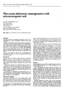
Von Neumann & Harvard microcontroller architectures Von Neumann and Harvard are two fundamental microcomputer architectures that respectively use a) the same and b) separate storage and signal pathways for instructions and data. Figure 11 presents the block diagram of a) Von Neumann and b) Harvard architectures.
Figure 1—1 a) Von Neumann and b) Harvard architectures
During the execution of a code, Von Neumann architecture obtains instructions and assigns data from/to the same memory, while Harvard architecture obtains instructions from one memory called program memory, and assigns data to another memory called data memory. Harvard architecture allows simultaneous access to both instructions and data and therefore optimizes system performance. The Harvard architecture scheme in association 1
AVR microcontrollers are actually of Modified Harvard architecture and able to use program memory as data memory (see the manufacture’s website for more specific information).
30
CH AP T ER 1 Mi cr oc o m pu t er ar c hi t ec t ur e
with RISC core architecture is used for a microcomputer system capable of achieving the same execution time for every individual instruction (and irrespective of the instruction complexity). One of the special features of Harvard architecture is that it can fetch and execute instructions that are stored in program memory [15]. On the other hand, Von Neumann architecture has the ability to fetch and execute instructions stored in both program and data memory. This particular feature of Von Neumann architecture provides the programmer with the ability to experiment with significant inner mechanisms 2 of the microcomputer system [16]. This is an additional reason for choosing the HC08 series of MCUs which are of Von Neumann architecture. Hereafter, the section presents the fundamental parts of a microcomputer system and focuses on 8-bit microcontrollers.
Central processing unit The CPU is considered the most significant part of the computer’s system and it is responsible for the execution of a computer program. Computer programs consist of machine instructions that are assigned to the computer’s memory. In conventional computer systems, programming is of sequential execution, that is, the CPU continuously fetches and executes instructions from memory in sequential order. The process by which the computer obtains and executes instructions from its memory is regularly referred to as the fetch-and-execute cycle. Machine instructions constitute binary numbers that describe the instruction operation code (opcode) as well as its argument(s). The instruction opcode describes the operation to be performed, while opcode format, instruction syntax, addressing modes, etc., are collectively referred to as the instruction set architecture (ISA) of the CPU. According to this information, instruction execution depends on the computer architecture and it is specified by the input clock frequency, which synchronizes the CPU internal mechanisms. Contrary to modern personal computers that operate with an input clock frequency of GHz, 8bit MCUs have a regular operating frequency of MHz. From the designer’s point of view, the CPU of a microcontroller consists of general purpose registers3 for reading/writing data from/to memory as well as performing arithmetic and bitwise operations. The length of the CPU registers specifies the system’s architecture. For example, an 8-bit CPU consists of 8-bit registers and 8-bit data bus. However, 8-bit CPUs can have special function registers of greater than 8-bit length. One of the fundamental special function registers is the program counter (PC). The program counter contains the address of the next instruction in memory to be fetched and executed. Thus, the length of this particular register determines the memory depth of the microcomputer system.
Memory Memory constitutes the physical device intended for the storage of information, that is, bits representing the program instructions and data. In microcontrollers, program instruc2 3
A corresponding example in assembly language is presented in Chapter 2. A hardware register in a computer system stores bits of information.
In tr o d uc ti o n t o mi cr o c o mp u t ers
31
tions are stored to non-volatile memory and program data (i.e., data occurring during the code execution) to volatile memory. While volatile memory requires power to retain information, non-volatile memory retains data even if it is not powered. Volatile storage is carried out in Random Access Memory (RAM). On the other hand, non-volatile storage is carried out in Read Only Memory (ROM) and, in particular, in Electrically Erasable Programmable Read Only Memory (EEPROM). Modern 8-bit microcontrollers use an alternative type of EEPROM, known as Flash memory. Contrary to the regular byte-to-byte erasing and storage of information in EPROM, Flash memory is erased and rewritten in large blocks and thus it is characterized by faster access times. Usually, Flash memory in 8-bit MCUs is counted in kilobytes (KB), while RAM is counted in bytes (B). A byte is a unit of digital information and it is equal to eight bits, where every bit defines two possible states, the logic ‘1’ and ‘0’ state. Table 11 presents the multiples of bytes.
Table 1—1 Multiples of byte
Another concept that is of particular significance in regard to memory usage is the assignment of numbers greater than 1-byte, in memory formed of 1-byte registers [17]. For example, the assignment of the hexadecimal 4 number 0x1234ABCD can be carried out either in a) big-endian or b) little-endian ordering (Figure 12). In computing, the term endianness refers to the particular order in which large data are stored to memory. In bigendian ordering, storage initiates from the most significant byte, while in little-endian ordering, storage initiates from the least significant byte.
Figure 1—2 a) Big-endian and b) Little-endian ordering
Input/output devices Input/output (i/o) devices constitute that hardware part of the computer system which is used for the communication with the outside world. In microcontrollers, i/o devices end at the device pins, to which the designer connects i/o peripheral units in order to either receive
4
Positional numeral systems are examined in detail in Chapter 3.
CH AP T ER 1 Mi cr oc o m pu t er ar c hi t ec t ur e
32
or transmit data from/to the outside world. As expected, the regular peripheral units of microcontroller applications are much simpler than the regular peripheral units of personal computers. Some of the most familiar are: mechanical switches, matrix keyboards, light emitter diodes (LEDs), seven-segment displays, liquid crystal displays (LCDs), etc. The control of peripheral devices is managed through digital signals of logic ‘1’ and ‘0’, where the range of their voltage levels depends on the device type being used. In the practical examples of the book, binary ‘1’ refers to 5V level (active-high signal) and binary ‘0’ to 0V level (active-low signal). In some cases, however, there is a need to recognize and specify voltage levels of other than active-high and active-low (such as in temperature measurement, humidity measurement, etc.). Thus, microcontroller-based applications often require analog to digital converters (ADCs) for the administration of analog signals, whereas modern MCUs are designed with embedded ADCs. The control of the microcontroller’s i/o devices (as well as its embedded subsystems) is achieved through special function registers, also known as i/o registers.
Embedded system design The design of an MCU-based application is often referred to as embedded system design. In general, an embedded system is a computer-based system designed for a specific purpose application. The development of an embedded system incorporates the hardware design (i.e., the selection of the appropriate computer system, the definition of the requisite i/o units and relevant electronic components, the printed circuit board design, etc.) along with the software development for the control of hardware. Due to the fact that the software running on the embedded system is a fixed program, it is regularly called firmware.
Figure 1—3 Block diagram of a typical embedded system
In tr o d uc ti o n t o mi cr o c o mp u t ers
33
The firmware development process for a microcontroller relies on inputting/outputting data from/to the outside world, as well as the processing of information. Contrary to the software development process in high-level programming, firmware development in lowlevel programming entails a deep understanding of the microcomputer architecture, as well as an awareness of handling the application peripherals. The abundant examples that make use of microcontrollers include, but are not limited to, industrial automation, telecommunication systems, automotive applications, and consumer electronics. The typical block diagram of a microcontroller-based system is given in Figure 13.
34
CH AP T ER 1 Mi cr oc o m pu t er ar c hi t ec t ur e
1.2 The central processing unit CPU08 This section focuses on the central processing unit CPU08 [18] (that is, the CPU of the M68HC08 family of units) and explores its special features. The study of the CPU08 is necessary for an easy passage to the subsequent learning step, i.e., the assembly language programming of the M68HC908GP32 microcontroller.
General description Figure 14 presents the block diagram of the CPU08. The CPU08 is divided into a) the control unit and b) the execution unit.
Figure 1—4 CPU08 block diagram
The control unit consists of a Finite State Machine (FSM) which generates the synchronization signals of the execution unit. On the other hand, the execution unit (the unit responsible for executing a series of tasks described by the program code) consists of a) the arithmetic logic unit5 (ALU), b) CPU registers, and c) the bus interface between the CPU and memory. Figure 15 presents the five registers of the CPU08. These are a) the accumulator (A), b) the index register (H:X), c) the program counter (PC), d) the stack pointer (SP), and e) the condition code register (CCR).
Accumulator (Α) This 8-bit register can be treated as a general purpose register for holding operands, but its special purpose is to hold results of arithmetic and logical operation. There are a considerable number of assembly instructions dealing with the accumulator in order to carry out arithmetic or logical results. The accumulator’s value after a device reset is indeterminate (denoted X in Figure 15).
5
The ALU is the basic digital circuit of the central processing unit used to perform arithmetic and logical operations on integers.
T h e c e n tra l pr o c es si ng u ni t CP U 0 8
35
Figure 1—5 CPU08 registers
Index register (H:X) This 16-bit register is a concatenation of H and X registers and can be used as either a general purpose register or an index register for assigning/obtaining data to/from memory. For backwards compatibility purposes with the earlier M68HC05 family of MCUs, the index register can also be used as an 8-bit register, where in this particular case its upper byte should be set to zero (H=0). The register value after a device reset is indeterminate.
Program counter (PC) The program counter is a 16-bit register containing the addresses of the next instruction to be fetched. During the instruction execution, the address in the program counter automatically increments by an appropriate amount so as to point to the subsequent code instruction. However, an exception to this rule is justified whenever the instruction alters the regular program flow, or in the particular case where the microcontroller responds to an interrupt6 mechanism. During a reset, the program counter is assigned to the address located at the reset vector (denoted R in Figure 15). Thus, the designer should initialize the reset vector to the address of the opening code instruction in every single program.
Stack pointer (SP) The stack pointer is a 16-bit register containing the address of the next available location on the stack. The concept of the stack refers to the way the microcontroller’s data memory (RAM) is used as last-in-first-out (LIFO) memory. One of the most important uses of the stack is in line with the program flow of control. For instance, whenever performing a call to a program’s routine, the CPU automatically pushes the value of the program counter onto the stack. After the execution of the routine’s instructions, the CPU pulls the program counter from the stack in order to resume the program flow. The value of the stack pointer dec-
6
Interrupts are explained later in this section.
36
CH AP T ER 1 Mi cr oc o m pu t er ar c hi t ec t ur e
rements as data are pushed onto the stack, while it increments as data are pulled from the stack. The stack pointer can also be used as an index register to access data on the stack. For backwards compatibility purposes with the earlier M68HC05 family of MCUs, the stack pointer is assigned the value 0x00FF during a device reset. However, the stack can be relocated by the designer to anywhere within the data memory.
Condition code register (CCR) The condition code register is an 8-bit register consisting of flags which indicate either the result of an instruction execution or the result of inner tasks performed by the MCU. Carry/borrow flag (C) When the CPU sets the carry/borrow flag to binary ‘1’, it indicates the generation of a carry/borrow during an operation. Zero flag (Z) When the CPU sets the zero flag to binary ‘1’, it indicates the generation of a zero result during an operation. Negative flag (Ν) When the CPU sets the negative flag to binary ‘1’, it indicates the generation of a negative value during an operation. Interrupt mask (Ι) The interrupt mask is used to manually activate (Ι=0) or deactivate (Ι=1) the microcontroller’s interrupt mechanisms. If an interrupt occurs, the I mask is automatically set to binary ‘1’ in order to prevent other interrupts disturbing the service of the current mechanism. In addition, all CPU registers are pushed onto the stack, except the H register, in order to maintain compatibility with the earlier M68HC05 family of MCUs. However, the designer can manually stack or unstack the H register through PSHH (Push H onto stack) and PULH (Pull H from stack) instructions correspondingly. After servicing the interrupt, the CPU registers are pulled from the stack and the I mask is cleared. Simultaneous interrupts with lower priority are latched and serviced as soon as the I mask is cleared. Half-carry flag (H) When the CPU sets the half-carry flag to binary ‘1’, it indicates the generation of carry between the third and fourth bits of the accumulator. This flag is used for binary-codeddecimal (BCD)7 arithmetic operations. Overflow flag (V) When the CPU sets the overflow flag to binary ‘1’, it indicates a two’s complement8 overflow during an arithmetic operation. The overflow flag is controlled by the following signed instructions that are used for the program flow of control: BGT (Branch if greater than), BGE (Branch if greater than or equal to), BLE (Branch if less than or equal to), BLT (Branch if less than).
7 8
BCD digital encoded method is examined in Chapter 3. Signed number representations are presented in Chapter 3.
T h e c e n tra l pr o c es si ng u ni t CP U 0 8
37
Functional description The CPU08 can enter two different modes of operation, that is, the monitor and user mode [19, 20]. In monitor mode, the CPU executes code that has been permanently stored into memory and it is used to provide an asynchronous serial communication between the microcontroller and a host computer. In this mode it is possible to load into the microcontroller’s memory an assembled binary code, as well as to perform in-circuit simulation/debugging of the code. In user mode, the CPU executes the user-defined code that has been previously loaded into the program memory. The mode which the CPU08 enters depends on the logic level on the IRQ pin after power-on reset (POR). A CPU reset causes all registers to be loaded to their default values and all modules to return to their initial state. If the CPU08 enters user mode, then the program counter is assigned to the address located at the reset vector9 and consequently the code execution starts from this particular memory address. The CPU08 is designed to access memory of 64KB (216=65536B=64KB) depth and 8-bit length. Therefore, each memory location is identified by a 16-bit number (216=65536), while it can receive values in the range 0 to 255 (2 8=256). This is the reason why the reset vector is defined by two memory addresses, as their concatenation forms the 16-bit starting address. During the execution of an instruction, the value in the program counter increments by the amount of bytes reserved for this particular instruction. For example, if the storage of the leading instruction begins at memory address 0x8000 and reserves three bytes in memory, then the following actions are performed. First, the program counter gets the value 0x8000 from the reset vector, and during the instruction execution it increments its value by three (i.e., the value in the program counter changes from 0x8000 to 0x8003) so as to point the subsequent code instruction. This programming approach is also known as sequential programming. In sequential programming, it is often necessary to alter the normal program flow. Thus, the CPU08 consists of instructions that perform conditional or unconditional branching, as well as interrupt mechanisms that cause normal program flow to be suspended. Unconditional branching instructions admit a label for argument and alter the program flow to the effective address identified by the label. The same actions perform instructions that are used for calling a program routine 10. During this call the program counter increments by the amount of bytes that are reserved by this – call to subroutine – instruction. Then the program counter is pushed onto the stack and afterwards it is loaded to the effective address described by the subroutine label. The program flow enters the subroutine code and the last instruction of the subroutine (which is a specific instruction of particular purpose) pulls the program counter from the stack and resumes program flow. Conditional branching instructions have a similar function, except that branching occurs in the event that the evaluated condition is considered to be true, while if it is false, the program continues to the next-in line instruction. These instructions evaluate the condition code register flags and therefore it is expected that the preceding instruction(s) will have an effect on
9
The Reset vector of the M68HC908GP32 refers to memory addresses 0xFFFE and 0xFFFF. Assembly language routines (also known as subroutines) are parts of code that are written just once in the program and can be called as many times as needed. 10
38
CH AP T ER 1 Mi cr oc o m pu t er ar c hi t ec t ur e
these flags. The program flow can also be altered through an interrupt mechanism. Interrupts cause the program flow to be suspended in order to provide an immediate service to the interrupt mechanism, i.e., to straightforwardly respond to an event and execute a group of instructions within an interrupt service routine (ISR). After finishing the execution of the ISR, the CPU resumes the program flow through the execution of a special function instruction. This procedure is similar to the subroutine call/return operation.
Interrupt processing Although it is possible to perform an interrupt through the assembly code (also known as software interrupt), in general, interrupts constitute automatic responses of the hardware. Interrupt processing requires a series of initialization steps before being utilized. The first step is the activation of the interrupt mechanism that the designer would like to use. The activation is achieved by instructions that store specific values to one or more registers. Then the designer writes the ISR that is executed in response to the interrupt mechanism. Finally, the designer assigns to the corresponding interrupt vector the effective address of the ISR. As concerns the M68HC908GP32 MCU, the CPU08 can reach up to 127 interrupt vectors for 127 independent interrupt sources (including software interrupt). The CPU08 vectors (including the reset vector) are presented in Table 12.
Table 1—2 CPU08 FLASH vectors
The vector position is proportional to the interrupt priority. Thus, if two or more interrupts occur at the same time, then priority decoding 11 it is performed to the corresponding sources, and their service is carried out in succession. During the service on an interrupt, the I mask in the CCR is automatically set to binary ‘1’ in order to prevent other interrupts disturbing the current service. The only mechanism not affected by the I mask is the software interrupt. The program flow resumes with the execution of a specific instruction that is routinely placed at the end of each ISR, which also clears the I mask. During a call to interrupt, the CPU registers are pushed onto the stack in the following order12: PC (loworder byte), PC (high-order byte), Χ (index register low), Α, CCR. One of the numerous applications of interrupts is to awaken the MCU after it has been put in a low-power state. The CPU08 has two different low-power modes of operation, the stop and wait mode. In stop mode, the CPU and bus clocks are disabled, while in wait mode, the CPU clock is disabled but the bus clock continues to run.
11
Priority decoding is achieved by an internal peripheral that is called the System Integration Module (SIM). The SIM and CPU08 together control all the internal functions of the microcomputer system. 12 CPU registers are pulled from the stack in reverse order.
T h e c e n tra l pr o c es si ng u ni t CP U 0 8
39
Addressing modes Addressing modes are considered part of the CPU instruction set architecture and define the way the CPU identifies operands of the machine instructions and accesses data. Assembly language instructions consist of an operation code (opcode) describing the operation(s) being performed during the instruction execution and, optionally, of one or more operands necessary for the processing of information. Operands define either a memory location or an integer value. Opcodes and operands are represented by binary digits (bits) that are stored to the microcomputer’s memory. The CPU08 employs six different addressing modes that are subsequently extended to sixteen with their subcategories [18]. A brief description of the six fundamental addressing modes is given hereafter.
Table 1—3 Inherent addressing instructions
40
CH AP T ER 1 Mi cr oc o m pu t er ar c hi t ec t ur e
Inherent Inherent instructions take no argument (operand), while most of them reserve only one byte in program memory. Inherent instructions are presented in Table 13.
Immediate Immediate instructions take an operand of constant value, and therefore the operand is characterized by the sharp (#) prefix. The sharp (#) symbol is used to describe an integer value rather than the value of a memory location, while the operand can reserve two or three bytes in program memory. Immediate instructions are presented in Table 14.
Direct Direct instructions can only access the first 256 memory locations (i.e., 0x00-0xFF), which is the area of memory that is used as RAM in many MCUs. The high order byte of the operand’s effective address is considered to be of zero value (0x0000-0x00FF), and thus each instruction reserves only two bytes in program memory. This addressing mode saves space and speeds up the execution time from the equivalent extended mode of 3-byte instructions. Direct instructions are presented in Table 15.
Extended Extended instructions can access any address in a 64-KB memory and they therefore reserve three bytes in program memory. At this point it is worth noting that the designer does not have to specify whether an instruction is of extended or direct mode, since the assembler automatically decodes this information in regard to the optimal implementation of the code at the machine level. Extended instructions are presented in Table 16.
Table 1—4 Immediate addressing instructions
Indexed Indexed instructions make use of either the index (H:X) register or the stack pointer. In each case the employed register suggests the offset from the memory location defined by
T h e c e n tra l pr o c es si ng u ni t CP U 0 8
41
the operand. Offset (8-bit or 16-bit) length is defined by the address of the operand. There are seven types of indexed addressing mode, of which five make use of the H:X register, while the other two utilize the stack pointer. These seven types are: a) indexed, no-offset, b) indexed, no-offset & post increment, c) indexed, 8-bit offset, d) indexed, 8-bit offset & post increment, e) indexed, 16-bit offset, f) stack pointer, 8-bit offset, g) stack pointer 16-bit offset. Indexed instructions are presented in Table 17, where instructions in bold letters refer to the option of performing a post increment to index.
Table 1—5 Direct addressing instructions
Table 1—6 Extended addressing instructions
42
CH AP T ER 1 Mi cr oc o m pu t er ar c hi t ec t ur e
Table 1—7 Indexed addressing instructions
Table 1—8 Relative addressing instructions
T h e c e n tra l pr o c es si ng u ni t CP U 0 8
43
Relative Relative instructions alter the program flow through a conditional branch. The branching offset ranges from -128 to +127 in regard to the memory address found immediately after the branch instruction. Relative instructions are presented in Table 18.
44
CH AP T ER 1 Mi cr oc o m pu t er ar c hi t ec t ur e
1.3 The M68HC908GP32 microcontroller unit This section explores the special features of the M68HC908GP32 [4] microcontroller and attempts to familiarize readers with this particular device. Readers may also use this section as a reference guide, whenever they need to look for particular technical specifications.
Features, pin assignment, pin function The MC68HC908GP32 is a general purpose and low cost microcontroller unit that incorporates the CPU08. The microcontroller features are: 32KB Flash memory, 512Β RAM, 33 i/o pins, low-power design, 3V or 5V operation, and 8MHz internal bus (maximum) frequency. The device also embeds several peripheral systems intended for more sophisticated applications, while it is addressed in packages of 40, 42 and 44 pins (PDIP, SDIP, and QFP correspondingly). Figure 16 presents the popular 40-pin PDIP pin assignments of MC68HC908GP32, which is the package used in the educational board that is proposed by the book. Pin functions are presented hereafter.
Figure 1—6 MC68HC908GP32 pin assignment (40-pin PDIP)
Power supply pins (VDD & VSS) The MC68HC908GP32 operates over a single supply voltage connected to the VDD and VSS (ground) pins. To avoid noise problems it is suggested that a 100nF bypassing capacitor is connected as close as possible to the device. Oscillator pins (OSC1 & OSC2) The input clock that synchronizes the CPU is connected to the OSC1 and OSC2 pins. If
T h e M6 8 HC 9 0 8GP 32 m ic ro c o ntr o ll er u nit
45
using a crystal oscillator, then its output should be connected to the OSC1 pin, while the OSC2 pin should be left floating. The maximum allowed (external) frequency is 20MHz and in the microcontroller’s standard (default) mode of operation it is internally divided by 4 (so generating 5MHz internal operating frequency). External reset pin (RST) The reset pin forces the MCU to a known start up state whenever it detects a binary ‘0’. Active-low voltage is regularly applied to the pin through a mechanical switch, while the pin is internally connected to a pull-up resistor. (The RST pin is bidirectional, allowing a reset of the external peripherals in particular circumstances.) External interrupt pin (IRQ) The IRQ pin forces the MCU to suspend normal program flow and execute the interrupt service routine that is associated with the external interrupt mechanism. The IRQ pin is asynchronous and it is internally connected to a pull-up resistor. CGM power supply (VDDΑ & VSSΑ) The VDDΑ & VSSΑ pins provide power supply to an embedded peripheral known as the clock generator module (CGM). The pins are connected to the same voltage potential as the main power supply pins, while same decoupling techniques should be also used with them. External filter capacitor pin (CGMXFC) This pin is intended for the connection of an external filter to the clock generator module in the event that subsystem makes use of the phase-locked-loop (PLL) unit. ADC power supply/reference pins (VDDΑD & VSSΑD) The VDDΑD & VSSΑD pins are power supply pins for the embedded analog to digital converter. The pins are connected to the same voltage potential as the main power supply pins, while the same decoupling techniques should be also used with them. Port A I/O pins (PTA7-PTA0) The PTA7 to PTA0 are general purpose and bidirectional i/o pins that provide an interface to the outside world. Each pin can be independently defined to be either input or output13, and if it is defined to be input, then an internal pull-up resistor is available for this pin. These pins can be configured to operate as keyboard interrupt pins when using the keyboard interrupt module. Port B I/O pins (PTB7-PTB0) The PTB7 to PTB0 are general purpose and bidirectional i/o pins that provide an interface to the outside world. These pins can be configured to operate as inputs to the embedded analog to digital converter. Port C I/O pins (PTC4-PTC0) The PTC4 to PTC0 are general purpose and bidirectional i/o pins that provide an interface to the outside world. Each pin can be independently defined to be either input or output, and if it is defined to be input, then an internal pull-up resistor is available for this pin. Port D I/O pins (PTD5-PTD0) The PTD5 to PTD0 are general purpose and bidirectional i/o pins that provide an inter-
13
It is suggested that any unused pin or i/o port should be connected to VDD or VSS so as to prevent static electricity damage.
46
CH AP T ER 1 Mi cr oc o m pu t er ar c hi t ec t ur e
face to the outside world. Each pin can be independently defined to be either input or output, and if it is defined to be input, then an internal pull-up resistor is available for this pin. The PTD5 and PTD4 can be configured to operate as timer interface module (TIM) pins, while the PTD3 to PTD0 can be configured to operate as serial peripheral interface (SPI) pins. Port E I/O pins (PTE1, PTE0) The PTE1 and PTE0 are general purpose and bidirectional i/o pins that provide an interface to the outside world. These pins can be configured to operate as serial communications interface (SCI) pins.
Figure 1—7 M68HC908GP32 memory map
Memory map The control of the microcontroller’s i/o pins and embedded peripherals is achieved by special function registers located in the memory. These registers are called i/o registers and they are divided into three categories: a) control registers, b) status registers, and c) data
T h e M6 8 HC 9 0 8GP 32 m ic ro c o ntr o ll er u nit
47
registers. Figure 17 presents a general aspect of the M68HC908GP32 memory map 14, while Table 19 presents i/o registers and Table 110 presents vector addresses of this particular MCU. For more specific information, the designer may refer to the microcontroller’s technical data [4] or to the relevant reference manuals [21-24] delivered by Motorola literature distribution. Memory address 0x0000 0x0001 0x0002 0x0003 0x0004 0x0005 0x0006 0x0007 0x0008 0x0009 0x000A 0x000B 0x000C 0x000D 0x000E 0x000F 0x0010 0x0011 0x0012 0x0013 0x0014 0x0015 0x0016 0x0017 0x0018 0x0019 0x001A 0x001B 0x001C 0x001D 0x001E 0x001F 0x0020 0x0021 0x0022 0x0023 0x0024 0x0025 0x0026 0x0027 0x0028 0x0029
14
Register description Port A Data Register Port B Data Register Port C Data Register Port D Data Register Data Direction Register A Data Direction Register B Data Direction Register C Data Direction Register D Port E Data Register Unimplemented Unimplemented Unimplemented Data Direction Register E Port A Input Pullup Enable Register Port C Input Pullup Enable Register Port D Input Pullup Enable Register SPI Control Register SPI Status and Control Register SPI Data Register SCI Control Register 1 SCI Control Register 2 SCI Control Register 3 SCI Status Register 1 SCI Status Register 2 SCI Data Register SCI Baud Register Keyboard Status and control Register Keyboard Interrupt Enable Register Time Base Module Control Register IRQ Status and Control Register Configuration Register 2 Configuration Register 1 Timer 1 Status and Control Register Timer 1 Counter Register High Timer 1 Counter Register Low Timer 1 Counter Modulo Register High Timer 1 Counter Modulo Register Low Timer 1 Channel 0 Status and Control Register Timer 1 Channel 0 Register High Timer 1 Channel 0 Register Low Timer 1 Channel 1 Status and Control Register Timer 1 Channel 1 Register High
Abbreviation PTA PTB PTC PTD DDRA DDRB DDRC DDRD PTE U U U DDRE PTAPUE PTCPUE PTDPUE SPCR SPSCR SPDR SCC1 SCC2 SCC3 SCS1 SCS2 SCDR SCBR INTKBSCR INTKBIER TBCR INTSCR CONFIG2 CONFIG1 T1SC T1CNTH T1CNTL T1MODH T1MODL T1SC0 T1CH0H T1CH0L T1SC1 T1CH1H
Accessing the unimplemented locations presented in Figure 17 may cause an illegal address reset to the microcontroller from the system integration module. Moreover, accessing the reserved memory locations may cause an unpredictable effect in the device.
CH AP T ER 1 Mi cr oc o m pu t er ar c hi t ec t ur e
48
Memory address Register description Abbreviation 0x002A Timer 1 Channel 1 Register Low T1CH1L 0x002B Timer 2 Status and Control Register T2SC 0x002C Timer 2 Counter Register High T2CNTH 0x002D Timer 2 Counter Register Low T2CNTL 0x002E Timer 2 Counter Modulo Register High T2MODH 0x002F Timer 2 Counter Modulo Register Low T2MODL 0x0030 Timer 2 Channel 0 Status and Control Register T2SC0 0x0031 Timer 2 Channel 0 Register High T2CH0H 0x0022 Timer 2 Channel 0 Register Low T2CH0L 0x0033 Timer 2 Channel 1 Status and Control Register T2SC1 0x0034 Timer 2 Channel 1 Register High T2CH1H 0x0035 Timer 2 Channel 1 Register Low T2CH1L 0x0036 PLL Control Register PCTL 0x0037 PLL Bandwidth Register PBWC 0x0038 PLL Multiplier Select High PMSH 0x0039 PLL Multiplier Select Low PMSL 0x003A PLL VCO Range Select Register PMRS 0x003B PLL Reference Divider Select Register PMDS 0x003C Analog-to-Digital Status and Control Register ADSCR 0x003D Analog-to-Digital Data Register ADR 0x003E Analog-to-Digital Clock Register ADCLK 0x003F Unimplemented U 0xFE00 SIM Break Status Register SBSR 0xFE01 SIM Reset Status Register SRSR 0xFE02 SIM Upper Byte Address Register SUBAR 0xFE03 SIM Break Flag Control Register SBFCR 0xFE04 Interrupt Status Register 1 INT1 0xFE05 Interrupt Status Register 2 INT2 0xFE06 Interrupt Status Register 3 INT3 0xFE07 Reserved R 0xFE08 FLASH Control Register FLCR 0xFE09 Break Address Register High BRKH 0xFE0A Break Address Register Low BRKL 0xFE0B Break Status and Control Register BRKSCR 0xFE0C LVI Status Register LVISR 0xFF7E FLASH Block Protect Register FLBPR 0xFFFF COP Control Register COPCTL Table 1—9 M68HC908GP32 control, status, and data registers Memory address 0xFFFF 0xFFFE 0xFFFD 0xFFFC 0xFFFB 0xFFFA 0xFFF9 0xFFF8 0xFFF7 0xFFF6 0xFFF5 0xFFF4 0xFFF3 0xFFF2 0xFFF1
Vector description Reset Vector (Low) Reset Vector (High) SWI Vector (Low) SWI Vector (High) IRQ Vector (Low) IRQ Vector (High) PLL Vector (Low) PLL Vector (High) TIM1 Channel 0 Vector (Low) TIM1 Channel 0 Vector (High) TIM1 Channel 1 Vector (Low) TIM1 Channel 1 Vector (High) TIM1 Overflow Vector (Low) TIM1 Overflow Vector (High) TIM2 Channel 0 Vector (Low)
T h e M6 8 HC 9 0 8GP 32 m ic ro c o ntr o ll er u nit
49
Memory address Vector description 0xFFF0 TIM2 Channel 0 Vector (High) 0xFFEF TIM2 Channel 1 Vector (Low) 0xFFEE TIM2 Channel 1 Vector (High) 0xFFED TIM2 Overflow Vector (Low) 0xFFEC TIM2 Overflow Vector (High) 0xFFEB SPI Receive Vector (Low) 0xFFEA SPI Receive Vector (High) 0xFFE9 SPI Transmit Vector (Low) 0xFFE8 SPI Transmit Vector (High) 0xFFE7 SCI Error Vector (Low) 0xFFE6 SCI Error Vector (High) 0xFFE5 SCI Receive Vector (Low) 0xFFE4 SCI Receive Vector (High) 0xFFE3 SCI Transmit Vector (Low) 0xFFE2 SCI Transmit Vector (High) 0xFFE1 Keyboard Vector (Low) 0xFFE0 Keyboard Vector Vector (High) 0xFFDF ADC Conversion Complete Vector (Low) 0xFFDE ADC Conversion Complete Vector (High) 0xFFDD Timebase Vector (Low) Vector (High) 0xFFDC Timebase Vector (High) Table 1—10 M68HC908GP32 vector addresses
Embedded peripherals This subsection provides a brief description of the M68HC908GP32 embedded peripherals. However, analytical description of each peripheral has been purposely avoided since the best way of understanding them is accomplished through a practical examination of their internal mechanism. Most of the embedded systems are examined in practice in chapters 4 and 5.
Analog to digital converter (ADC) The analog to digital converter consists of a successive approximation design of eight input channels (and 8-bit resolution per channel), which share function with the PTB7 to PTB0 i/o pins and are used for sampling external analog signals. As soon as the conversion of the input signal finishes, the module stores the results in its data register and sets a flag or generates an interrupt.
Break module (BRK) The break module generates an interrupt that causes program flow to be suspended at a particular memory location in order to enter a background program.
Clock generator module (CGM) The clock generator module produces the internal synchronization clock of the CPU. The module also contains a phase-locked-loop design.
50
CH AP T ER 1 Mi cr oc o m pu t er ar c hi t ec t ur e
Computer operating properly (COP) The computer operating properly module monitors the approved operation of the MCU and generates a reset signal in the event that the program flow illegally stops at a memory location. This operation is accomplished though a free-running counter that is included in the module.
External interrupt (IRQ) The external interrupt module provides an interrupt to the microcontroller whenever a binary ‘0’ is applied to the corresponding pin.
Keyboard interrupt module (KBI) The keyboard interrupt module provides eight different external interrupts to the microcontroller through the PTA7 to PTA0 pins. When a port pin is enabled for KBI function, a pull-up resistor is internally connected to this pin.
Low-voltage inhibit (LVI) The low voltage inhibit module monitors the voltage potential on the VDD pin and forces the MCU to reset state if the voltage drops below the LVI trip falling voltage (VTRIPF).
Serial communication interface module (SCI) The serial communication interface module provides an asynchronous serial interface between the microcontroller and other peripheral devices.
System integration module (SIM) The system integration module coordinates the CPU08 and exception timing in order to control all MCU activities such as bus clock generation and control for CPU and peripherals, master reset control, interrupt control, etc.
Serial peripheral interface module (SPI) The serial peripheral interface provides a synchronous, full-duplex serial interface between the microcontroller and other peripheral devices.
Timebase module (TBM) The timebase module generates periodic interrupts at eight selectable rates defined by the designer. (The module allows periodic wake up of the microcontroller during stop mode.)
Timer interface module (TIM) The timer interface module consists of a two-channel timer that can be used either as a
T h e M6 8 HC 9 0 8GP 32 m ic ro c o ntr o ll er u nit
51
free-running (modulo) up counter, or a timing reference with input capture, output compare and pulse width modulation (PWM) functions.
CH AP T ER 1 Mi cr oc o m pu t er ar c hi t ec t ur e
52
1.4 Practice problems 1.4.1 1.4.2 1.4.3 1.4.4 1.4.5 1.4.6 1.4.7 1.4.8 1.4.9 1.4.10 1.4.11 1.4.12 1.4.13 1.4.14 1.4.15 1.4.16 1.4.17 1.4.18
Describe the term computer. Define the differences between the CISC and RISC core architectures. Define the differences between the Von Neumann and Harvard architectures. Describe the main purpose of the CPU. Define the regular operating frequency of microcontrollers (i.e., Hz, KHz, etc.). Define the differences between a volatile and non-volatile memory. Define the differences between Flash and EEPROM. Calculate the number of bytes in a 32KB memory. Place the hexadecimal number 0xABCDEF896745 to the first addresses of a 256Β memory of 8-bit length using a) big-endian and b) little-endian ordering. Describe the control of peripheral devices through a MCU. Create the block diagram of a typical microcontroller-based system. Create and describe the block diagram of the CPU08. Calculate the effective offset achieved by a) index register (H:X) and b) index register low (Χ). Describe the concepts of stack and LIFO memory. Define the difference between monitor and user mode of operation of the CPU08. Describe the general idea of an interrupt processing. Is it possible to generate an interrupt of the CPU08 during the service of a different interrupt? Define the endianness that is used in the M68HC08 family of units for the operand assignment in program memory.
Re f er e nc e s
53
1.5 References [1] Microcomputer (on-line): http://en.wikipedia.org/wiki/Microcomputer. [2] 8-bit never dies. Pixel magazine (in Greek), Compupress S.A., Cholargos, 2007. [3] M68HC05 family: understanding small microcontrollers. Motorola Literature Distribution, Denver Colorado, 1998. [4] M68HC908GP32 M68HC08GP32 technical data (rev. 6), Motorola Literature Distribution, Denver, Colorado, 2002. [5] http://www.freescale.com (on-line). [6] http://www.pemicro.com (on-line). [7] http://www.microchip.com (on-line). [8] http://www.atmel.com (on-line). [9] http://www.maxim-ic.com (on-line). [10] D. E. Bolanakis, K. T. Kotsis and T. Laopoulos, “Teaching Concepts in Microcontroller Education: CISC vs RISC assembly-level programming”, in Proc. of the International Conference on Information Communication Technologies in Education (ICICTE 2009), 9-11 July 2009, Corfu, Greece, pp. 742-750. [11] V. P. Heuring and H. F. Jordan, “Computer Systems Design and Architecture (2 nd ed.)”, Publishing House of Electronics Industry, Beijing, 2004. [12] H. El-Aawar, “CISC vs RISC hardware and programming complexity measures of addressing modes”, in Proc. of the International Conference on Perspective Technologies and Methods in MEMS Design (MEMSTECH), 24-27 May 2006, Lviv-Polyana, Ukraine. [13] G. Myklebust, “The AVR microcontroller and C compiler co-design”, in Proc. of the 3rd Euro. Microprocessor and Microcontroller Seminar, 6 November 1996, Heathrow, U.K., pp. 164–170. [14] J. R. Richardson, “Effectively teaching C in an introductory embedded microcontroller course”, in Proc. of the ASEE IL/IN Sectional Conference, 1-2 April 2005, DeKalb, Illinois, pp. 1-8. [15] A. Francillon and C. Castelluccia, “Code injection attacks on Harvard-architecture devices”, in Proc. of the 15th ACM Conference on Computer and Communications Security (CCS’ 08), 27-31 October 2008, Virginia, USA, pp. 1-11. [16] D. E. Bolanakis, G. A. Evangelakis, E. Glavas and K. T. Kotsis, “Teaching the Addressing Modes of the M68HC08 CPU by Means of a Practicable Lesson”, in Proc. of the 11th IASTED International Conference on Computers and Advance Technology in Education (CATE 2008), 29 September–1 October 2008, Crete, Greece, pp. 446-450. [17] D. E. Bolanakis, K. T. Kotsis and T. Laopoulos, “Arithmetic Operations in Assembly Language: Educators’ Perspective on Endianness Learning using 8-bit Microcontrollers”, IEEE 5th International Workshop on Intelligent Data Acquisition and Advanced Computing Systems: Technology and Applications (IDAACS'2009), 21-23 September 2009, Rende, Italy, pp. 600-604. [18] CPU08 Central Processor Unit reference manual (rev. 3.0), Motorola Literature Distribution, Denver, Colorado, 2001.
54
CH AP T ER 1 Mi cr oc o m pu t er ar c hi t ec t ur e
[19] T. J. Airaudi, In-circuit Programming of the Flash Memory Using the Monitor Mode for the MC68HC908GP32 (rev. 1), Motorola Literature Distribution, Denver, Colorado, 2001. [20] T. C. Lun, In-circuit Programming of Flash Memory in the MC68HC908GP32 (rev. 2.0), Motorola Literature Distribution, Denver, Colorado, 2000. [21] G. Racino, Resetting Microcontrollers during Power Transitions, Motorola Literature Distribution, Denver, Colorado, 1998. [22] Y.-T. Ng, Power-on, Clock Selection, and Noise Reduction Techniques for the Motorola M68HC908GP32, Motorola Literature Distribution, Denver, Colorado, 2001. [23] S. Arendrarik, Generating Clocks for HC908 MCU Families, Motorola Literature Distribution, Denver, Colorado, 2003. [24] S. Robb, Creating Efficient C Code for the MC68HC08, Motorola Literature Distribution, Denver, Colorado, 2000.
Low-level Programming lready in the early ’80s, educators urged on the relevance of the assembly level programming with microcomputer technology [1, 2]. Code development process for microcomputers requires a deeper insight into the mechanisms’ working. Moreover, mnemonic instructions allow total control over the machine instructions, and thus assembly is considered to be an effective programming language for microcomputers. In addition, the simplified architectures of microcomputers system ease the low-level programming process, while the composite architectures of personal computers complicate the procedure [3]. However, assembly is an unstructured programming language that raises comprehension difficulties to the tutees. Those difficulties are increased when tutees are already familiarized with high-level programming topics, as highlevel languages tend to hide the underlying hardware from the programmer. This chapter presents a pedagogy that makes the parallelization between the assembly level programming for 8-bit microcontrollers and higher level programming in C language [4]. It is well known that freshman engineering students regularly attend a compulsory course in C programming language. Therefore, the present pedagogy explores the composition of the basic C programming possibilities into the machine level. The pedagogy aims in facilitating the assembly language learning without considering the knowledge of C language prerequisite.
A
55
2 IN THIS CHAPTER Introduction to the assembly language programming This subchapter focuses on the assembly language syntax rules for the MC68HC908GP32 microcontroller unit (MCU). The subchapter explores the assembly code development process, the translation of the mnemonic instructions into the target microcontroller’s machine code, and the simulation of code execution. Some of the issues presented are: the assembler’s directives, the pseudo-opcodes, the operators, the use of labels and comments, etc. A pseudo high-level code strategy in assembly language This subchapter focuses on a pedagogy that makes the parallelization between the assembly level programming for 8-bit microcontrollers and higher level programming in C language, while also explores the composition of the basic high-level programming possibilities into the machine level. Some of the issues presented are: the program flow-of-control, the initialization and accessing of one-dimensional arrays in microcontroller’s program and data memory, the arithmetic and bitwise operations, the modular programming method, etc. A macro-code example in assembly language This subchapter presents a novel aspect of a macro-code example in assembly language. The macro-code implements a ‘for’-like iterative loop that explores the addressing modes of the MC68HC908GP32 MCU, while in addition addresses the reader to a close examination of the modular programming method in the assembly level.
CH AP T ER 2 L ow -l e v el pr og ra mmi n g
56
2.1 Introduction to the assembly language programming This subchapter focuses on the assembly language syntax rules for the Μ68HC08 [5] family of microcontroller units (MCUs) and addresses a simple example in assembly language for the MC68HC908GP32 MCU [6]. The subchapter aims in familiarizing readers with the fundamental concepts of low-level programming for 8-bit microcontrollers.
Code development process Code development process in assembly language for the MC68HC908GP32 microcontroller is achieved through an editor included in the ICS08GPGTZ1 software package. Assembly language source code is stored to a file of .asm extension, while it is converted into a binary file of .s19 extension (also known as s-record file) though the CASM08Z [7] assembler program. S-record object files encode programs and data files in a printable format and are used for the programming of the microcontroller’s memory, but they can also be used as input for code simulation and debugging by the simulator program included in the ICS08GPGTZ. From the very beginning we need to clarify the way of developing an assembly language program for a specific MCU. The condition of writing code in assembly language is a concern of many issues. The designer should be familiarized with the assembly mnemonics of a particular MCU, as well as the assembler directives, pseudo operation codes, syntax rules, etc., which all have an effect on the code translation into the target microcomputer’s machine code. A detailed description of the assembly code development process compatible to the CASM08Z assembler and MC68HC908GP32 MCU is presented hereafter.
Syntax rules Assembly language programs are peculiar to a specific syntax type. First of all, assembly operation codes (opcodes), i.e., the portion of a machine instruction describing the operation to be performed, should not be placed in the first column. At least one space character should be placed before the opcode. The first column of programs is reserved for labels, assembler directives and code comments. Because the assembly programs regularly address numerous labels starting from the first column, assembly text is regularly separated into multiple columns. Label
Instruction
Argument(s)
Assembly language programs are regularly written in three columns where the first column holds the labels, second column holds the opcodes, and third column holds the argument(s) of each instruction. Separation between two successive columns is accomplished
1
ICS08GPGTZ software package is described in Appendix Β.
In tr o d uc ti o n t o t h e as s e mbl y l a ng ua g e p ro gr am mi ng
57
by pressing the tabulator (tab) key, located at the upper-left side of a standard keyboard. Optionally, a fourth column may be utilized as a comment column where in this particular case, a semicolon (;) character must precede the comment2. The semicolon forces the assembler to discard (during the translation process) any information written after the character. If the entire line is intended to be comment line, then an asterisk (*) character could be used as well. ;This is a comment line in assembly language. *This is an alternative way of inserting comment lines in assembly language.
Due to the fact that the use of asterisks is limited to the first column only, asterisks are normally used for header comments, whereas semicolons are regularly used to make comments on particular code lines. Some comment examples are presented hereafter. *This is an example in assembly language for the use of comments. *Asterisk (*) character are used to insert header comments. *In the following we give a pseudo-code with explanatory comments. Label1 Instruction1 Instruction2
Argument(s)1
;Comment of code line 1 ;Line 2 without label and argument(s)
Labels are symbolic names referred to the memory addresses utilized within a program, while they are used to ease the code development process and make the program more readable. The CASM08Z assembler admits labels of length lower than or equal to 16 character, while it discards the additional characters used in labels of greater (than the allowed) width. Labels must begin with either a letter of the English alphabet, or an underscore (_) character. Rest of the label can contain any printable character except space, double quote ("), and single quote (') characters. In addition, the colon (:) character can only be used at the end of each label. Label examples are given below. Label: Label_1 _label labelExample:
Assembler directives Assembler directives refer to the assembler’s revered words that provide information associated to the assembly process, e.g., where the machine code is to be located within the memory. Table 21 presents the CASM08Z assembler directives. The caret (^) character indicates the place where the directive parameter should be positioned. The directives are regularly placed before the assembly instructions, while they are invoked by one of the following characters: slash (/), full stop (.), sharp (#), dollar ($). BASE assembler directive
2
If an assembly instruction takes no argument(s), the third line should be left blank.
58
CH AP T ER 2 L ow -l e v el pr og ra mmi n g
Arguments of the assembly instructions may refer to numbers and in this particular case, the prefix/suffix located immediately before/after the number indicates the positional numeral system that is used to express its value. The default numeral system for the assembler CASM08Z is the hexadecimal. Therefore, whenever the prefix/suffix is omitted the number is considered to be of hexadecimal positional notation. Table 22 presents the prefix and suffix of the commonly employed numeral systems in the assembly language programming. However, the CASM08Z default system can be modified using the BASE directive.
Table 2—1 CASM08Z assembler directives
The example given below3 indicates the use of prefixes and suffixes as well as the alternation of the default (hexadecimal) numeral system to decimal and binary using the BASE directive. The example makes use of the LDA (Load accumulator from memory) instruc-
3
Hereafter, every assembly instruction has an associated number so as to support the explanation of the code.
In tr o d uc ti o n t o t h e as s e mbl y l a ng ua g e p ro gr am mi ng
59
tion for assigning accumulator (A) to an immediate value. The sharp (#) character located at the very beginning of the LDA argument indicates that the accumulator is assigned to an immediate value. Otherwise, the absence of sharp character would force accumulator to be loaded to the content of the memory address determined by the number.
Table 2—2 Prefixes/suffixes that define the numeral system
1 2 3 4 5 6 7 8 9 10 11 12
LDA LDA LDA LDA LDA LDA LDA
#!255 #255t #%11111111 #11111111q #$FF #0FFh #0FF
LDA
#255
LDA LDA
#11111111 #'A'
$BASE 10t $BASE 2t
Code lines 1 and 2 assign the value 25510 to the accumulator using the corresponding prefix (!) and suffix (t). Lines 3 and 4 assign the same value to the accumulator, which is expressed in the binary (111111112) positional notation, using the corresponding prefix (%) and suffix (q). Lines 5 and 6 perform the same action using hexadecimal (FF 16) positional notation. In this particular case, if the hexadecimal number initiates with a letter (i.e., Α, Β, C, D, E or F) and expressed by suffix, then the number zero (0) should be placed at the beginning of the hexadecimal value. Line 7 performs the same operation without using suffix, as the default numeral system for the assembler CASM08Z is the hexadecimal. Line 8 changes the default numeral system to decimal. Therefore, the line 6 assigns to the accumulator the value 25510 without making use of the corresponding prefix or suffix. The similar operation is performed by lines 10 and 11 for the assignment of a binary value without the use of a prefix/suffix. At this point it is worth noting that CASM08Z assembler accepts the use of ASCII characters4 provided that the character is enclosed within single or double quotes. Thus, the line 12 assigns character ‘A’ to the accumulator, which is equal to the value 4116 (=6510). CYCLE_ADDER_ON & CYCLE_ADDER_OFF assembler directives The number of instruction cycles of any assembly instructions inserted between the
4
The American standard code for information interchange (ASCII) is presented in chapter 3.
CH AP T ER 2 L ow -l e v el pr og ra mmi n g
60
CYCLE_ADDER_ON and CYCLE_ADDER_OFF assembler directives, is printed on a file of .lst extension (also known as listing file). This file is generated by the assembly process of the source code (i.e the .asm file). At this point it is worth noting that during the assembly of the source code, the CASM08Z assembler produces the .s19 binary file and three more files as well. All files have the same name as the user-defined .asm file and are of .bak, .map, and .lst extension. The .bak file creates backup of the previously saved source code. The .map file reserves information needed for source level simulation and/or debugging (i.e., it makes it possible for the user to inspect source code during simulation/debugging process). The .lst file holds a backup of the source code at which it inserts some annotations, such as the memory addresses that hold the instructions, the cycles of each instruction, etc. The example below makes use of the NOP (No operation) instruction in order to present the functional operation of CYCLE_ADDER_ON & CYCLE_ADDER_OFF assembler directives. 1 2 3 4 5 6 7 8
NOP $CYCLE_ADDER_ON NOP NOP NOP $CYCLE_ADDER_OFF NOP NOP
The NOP instruction does nothing but consumes one CPU cycle, and thus it is used for delay purposes. During the assembly process of the source code, lines 2 and 6 of the above code force the assembler to store the number of instruction cycles of lines 3-5 (i.e., 3 CPU cycles) to the leasting (.lst) file. INCLUDE assembler directive Software programs can be broken down into smaller parts codes and saved in different source files5. In this particular technique, the main assembly program is of .asm extension, while the other source files (embedded to the main) are of .inc extension (also known as include files). INCLUDE directive copies to the main program (and to the position at which the directive is being invoked), the source code of the .inc file specified by its parameter. The following program presents the use of an INCLUDE directive that copies the ‘delay.inc’ source code between lines 1 and 3. It is assumed that the ‘delay.inc’ file contains only two NOP instructions. 1 2 3
LDA $INCLUDE 'delay.inc' LDA
#!255 #!254
Line 1 assigns the value 25510 to the accumulator. Line 2 is replaced by the two NOP instructions included in the ‘delay.inc’ file. Finally, line 3 assigns the value 25410 to the ac-
5
This software design technique is known as modular programming and it is examined in the next subsection.
In tr o d uc ti o n t o t h e as s e mbl y l a ng ua g e p ro gr am mi ng
61
cumulator. The above program is equivalent to the one presented below. 1 2 3 4
LDA NOP NOP LDA
#!255
#!254
At this point it is worth noting that, if the include file is found in a different location than the application file (i.e., the main assembly file), then the full access path should be defined by the INCLUDE parameter. In both cases, the parameter can be enclosed within single or double quotes. 1
$INCLUDE "c:\pemicro\include\test.inc"
An .inc file may contain the INCLUDE directives itself, but nested includes are limited to a maximum number of ten. MACRO & MACROEND assembler directives The use of MACRO & MACROEND directives is, in some way, similar to the use of the INCLUDE directive. These directives are used for the generation of a macro-instruction, that is, several assembly language statements embedded in a single code line. A macroinstruction begins with the MACRO directive and concludes with the MACROEND. A macro-instruction is also specified by a name that is placed immediately after the MACRO word. The following example presents the syntax of a macro-instruction that embeds two individual NOP instructions and it is defined by the identical name double_nop. 1 2 3 4
$MACRO double_nop NOP NOP $MACROEND
The definition of a macro-instruction takes place before the main assembly code, while the macro-instruction is invoked by its identical name. The following program presents the way of performing a call to the double_nop macro-instruction by the main assembly program. During the assembly of the code, line 2 is replaced by the two NOP instructions included in the double_nop macro-instruction. 1 2 3
LDA #!255 double_nop LDA #!254
The use of macro-instructions compared to the use of INCLUDE directives, has two essential advantages. The former is that macro-instructions admit the use of labels6, without causing any assembler errors in case a call to a particular macro-instruction is performed more than once. The latter advantage is that macro-instructions take parameter values, and they therefore are able to extend the low-level programming techniques. Access to the mac-
6
Macro-instruction labels should be no more than 10characters.
CH AP T ER 2 L ow -l e v el pr og ra mmi n g
62
ro-instruction parameters is accomplished with the percent (%) character, followed by a positive integer that refers to the parameter being invoked.
Table 2—3 CASM08Z assembler arithmetic and logical operators
Table 23 presents the acceptable arithmetic and logical operators of the CASM08Z assembler that are regularly used in macro-instruction. If the macro-instruction addresses more than one operators, or in case its parameter makes use of parentheses that define the priority of arithmetic operations7, then the parameters are placed inside braces ({}). 1 2 3 4 5 6
$MACRO macro_test (a,b) LDA #%1 NOP NOP LDA #%2 $MACROEND
The above program presents the syntax of a macro-instruction named macro_test, which admits two parameters (a and b). Line 2 assigns the value of parameter a to the accumulator, lines 3 and 4 execute the NOP instruction, and line 5 assigns the value of parameter b to the accumulator. The call to this particular macro-instruction is presented in the program below, where
7
If the use of parentheses is ignored, then the assembler follows the known priority rules for arithmetic.
In tr o d uc ti o n t o t h e as s e mbl y l a ng ua g e p ro gr am mi ng
63
line 1 replaces parameters a and b to the values 25510 and 25410 correspondingly, while line 2 performs the exact same operation but with the use of hexadecimal notation (i.e., FF16 and FE16). 1 2
macro_test !255,!254 macro_test $FF,$FE
Nested macro-instructions are only allowed in the improved version of CASM08Z assembler which is the CasmHC08_Pro8. An example of nested macro-instructions is given below, where line 3 performs a call to the double_nop macro instruction. 1 2 3 4 5
$MACRO macro_test (a,b) LDA #%1 double_nop LDA #%2 $MACROEND
SET, SETNOT & IF, ELSEIF, ENDIF assembler directives IF, ELSEIF and ENDIF directives determine the parts of code that will be assembled. The directives SET and SETNOT set the value of their parameter to true and false, respectively. Thus, the part of code located between the directives IF and ENDIF (or ELSIF) will be assembled if the parameter value is true, while the code located between IFNOT and ENDIF (or ELSIF) will be assembled if the parameter value is false. 1 2 3 4 5 6
$SET debug $IF debug LDA
#!255
$ELSEIF NOP $ENDIF
Line 1 of the above code sets the value of debug parameter to true. Line 2 evaluates the content of the parameter and since it is considered to be true, the code between IF and ELSIF (i.e., the LDA instruction) will be assembled. Therefore, the code between ELSIF and ENDIF (i.e., the NOP instruction) will not be assembled.
Assembler pseudo-opcodes The CASM08Z assembler allows a set of pseudo-opcodes in place of the assembly mnemonics, which aim in facilitating the low-level programming process. Table 24 presents the available pseudo-opcodes of the CASM08Z. Examples of using these pseudoopcodes are given hereafter. The pseudo-opcode EQU The following program uses EQU pseudo-opcode in order to associate the memory address 0x8000 to the label PROGRAM_MEMORY (line 1), and the memory address
8
See P&E Microcomputer Systems website (www.pemicro.com) for particular information.
CH AP T ER 2 L ow -l e v el pr og ra mmi n g
64 0x0040 to the label RAM_MEMORY9 (line 2). 1 2
PROGRAM_MEMORY RAM_MEMORY
EQU EQU
$8000 $0040
Table 2—4 CASM08Z assembler pseudo-opcodes
The pseudo-opcode ORG The following program uses the ORG pseudo-opcode (line 2) in order to set the assembler’s location counter to the memory address labeled PROGRAM_MEMORY, that is, the 0x8000 memory location. Therefore, the first NOP instruction is stored to the 0x8000 memory address and the second one is stored to the 0x800110. 1 2 3 4
PROGRAM_MEMORY
EQU ORG NOP NOP
$8000 PROGRAM_MEMORY
The pseudo-opcode FCB The following program uses the FCB pseudo-opcode in order to assign the string11 ‘HELLO’ to the program memory. Line 3 assigns ‘H’ character to the 0x8000 memory location, line 4 assigns ‘E’ to the 0x8001, line 5 assigns ‘L’ to the 0x8002, and so fourth. 1 2 3
9
PROGRAM_MEMORY
EQU ORG FCB
$8000 PROGRAM_MEMORY 'H'
It is reminded that the MC68HC908GP32 program memory ranges from 0x8000 to 0xFDFF and the data memory ranges from 0x0040 to 0x023F. 10 The NOP instruction reserves one memory byte. 11 In computer science, a string refers to a sequence of ASCII characters.
In tr o d uc ti o n t o t h e as s e mbl y l a ng ua g e p ro gr am mi ng 4 5 6 7
FCB FCB FCB FCB
65
'E' 'L' 'L' 'O'
Lines 3-7 of the above code are equivalent to the following single code line: 1
FCB
'HELLO'
Moreover, the addition of a label before the FCB pseudo-opcode initiates an array of n elements, while +n syntax denotes the accessing of the nth element of the list. Thus, line 3 of the above code initiates the one-dimensional list named ARRAY, while line 4 obtains the 4th array element (which is the character ‘O’), since the array indices start always from zero. 1 2 3 4
PROGRAM_MEMORY ARRAY
EQU ORG FCB LDA
$8000 PROGRAM_MEMORY 'HELLO' ARRAY+4
In case there is a demand for assigning numbers instead of ASCII characters to the MCU memory, then the numbers should be separated by a comma. The following example assigns the 1-byte numbers 0A16, 0B16, 0C16, 0D16, 0E16, 1510 and 111111112 to the memory locations 0x8000-0x8006, respectively. 1 2 3
PROGRAM_MEMORY
EQU ORG FCB
$8000 PROGRAM_MEMORY $0A,$0B,$0C,$0D,$0E,!15,%11111111
The pseudo-opcode FDB The use of the pseudo-opcode FDB is identical to the FCB except that the former defines word, instead of byte storage (i.e., 16-bit instead of 8-bit storage). The FDB pseudo-opcode is regularly associated to the storage of information in the CPU vectors, since they reserve two bytes of memory. The following program uses the FDB in order to assign the so-called reset vector12, to the memory address labeled PROGRAM_START. The reset vector of the MC68HC908GP32 is located at the memory addresses 0xFFFE & 0xFFFF. 1 2
PROGRAM_MEMORY RESET_VECTOR
3 4
EQU EQU
$8000 $FFFE
ORG FDB
RESET_VECTOR PROGRAM_START
5 6
ARRAY
ORG FCB
PROGRAM_MEMORY 'HELLO'
7
PROGRAM_START
LDA
ARRAY+4
12
It is reminded that during the MCU reset, the program counter is loaded to the address located at the reset vector.
CH AP T ER 2 L ow -l e v el pr og ra mmi n g
66
Lines 1, 2 associate memory addresses 0x8000 and 0xFFFE to the labels PROGRAM_MEMORY and RESET_VECTOR, respectively. Line 3 sets the CASM08Z location counter to the memory address labeled RESET_VECTOR (i.e., the 0xFFFE memory location). Thus, line 4 assigns the high-order byte of the 16-bit number labeled PROGRAM_START (i.e., the 0x80 value of the 0x8000 number) to the 0xFFFE memory location, and the low order byte (i.e., the 0x00 value of the 0x8000 number) to the 0xFFFF memory location. In a similar procedure, lines 5 and 6 assign the ARRAY elements to the memory locations 0x8000-0x8004, while storage of the LDA instructions starts at 0x8005 (i.e., opcode of the instruction is stored to the 0x8005 memory address). Since the PROGRAM_START label is placed before the LDA mnemonic, the microcontroller starts the program execution from the LDA instruction of line 7. The pseudo-opcode RMB The following program presents an alternative process for the generation of onedimensional arrays in data memory through the RMB pseudo-opcode. Line 6 sets the CASM08Z location counter to the memory address labeled RAM_MEMORY (i.e., the 0x0040), while line 7 reserves five addresses of RAM (i.e., 0x0040-0x0044). Lines 4 and 5 define the first mnemonic to be executed on the MCU startup, which is the code line 9. Thus, the microcontroller executes the codes lines 9-13 that successively obtain and load to the accumulator the five array elements located at data memory. 1 2 3 4 5 6 7
PROGRAM_MEMORY RESET_VECTOR RAM_MEMORY
ARRAY
8 9 10 11 12 13
EQU EQU EQU ORG FDB ORG RMB
$8000 $FFFE $0040 RESET_VECTOR PROGRAM_MEMORY RAM_MEMORY 5
ORG LDA LDA LDA LDA LDA
PROGRAM_MEMORY ARRAY+0 ARRAY+1 ARRAY+2 ARRAY+3 ARRAY+4
A simple program in assembly language This section examines the development and simulation of a simplified code in assembly language for the MC68HC908GP32. It is worth noting that the code avoids emphasizing on the sophisticated programming techniques, since the main purpose is to emerge the procedure that has to be followed in order formulate an executable – by the MCU – file.
The problem Formulate a program that transfers the string ‘HELLO’ to the pins of Port A.
In tr o d uc ti o n t o t h e as s e mbl y l a ng ua g e p ro gr am mi ng
67
Figure 2—1 Flowchart symbols
Flowchart One popular method of representing the process (or the algorithm) of a code is the flowchart type of diagrams. The formulation of a flowchart regularly precedes the code development process, as it constitutes an illustrative diagram that helps in building an errorfree code [8]. Figure 21 presents the flowchart symbols that are used in this book. The oval symbol signals the start (Figure 21 a)) as well as the end (Figure 21 b)) of a process. The parallelogram shows a data processing (Figure 21 c)). The rhombus represents a decision, while it also indicates the flow path in case the evaluated condition is considered to be true or false (Figure 21 d)). Finally, the circle (in association with a number) indicates the junction points of a flowchart that is divided into smaller parts (Figure 21 e)).
Figure 2—2 Flowchart of a simple program in assembly language
CH AP T ER 2 L ow -l e v el pr og ra mmi n g
68
Figure 22 presents the flowchart diagram of the simplified code examined in this section13.
Source code syntax The syntax of the assembly code for the MC68HC908GP32 is regularly divided into two main sections. The former upholds the initialization process of the employed peripheral systems, while the latter addresses the main program code. Data arrays and program routines14 are regularly placed to either the beginning, or the end of the code. Finally, every program addresses assembler pseudo-opcodes and/or directives that formulate a readable and easily upgradeable code. Initializing the MCU port pins This example requires the initialization of Port A pins that, according to the current problem, should be declared as output pins. Port A constitutes an input/output (i/o) device, and thereby the corresponding pins can be declared as either inputs or outputs. The initialization of Port A is accomplished through the data direction register A (DDRA) located at memory address 0x0004. This register consists of 8 bits15 and every bit initializes the direction of the corresponding port pin. For instance, the value of DDRA(bit0) determines the direction of Port A(pin0), the value of DDRA(bit1) determines the direction of Port A(pin1), and so fourth. If the value of DDRA(bitn) is set to binary ‘0’ then the corresponding pin is configured as input, and if set to binary ‘1’ then the pin is configures as output. It is worth noting that every pin can be individually configured as input or output, without taking into consideration the direction of the rest port pins. According to the procedure procedure, every pin of Port A device in this particular example should be declared as output. Therefore, each bit of the DDRA register (i.e., the 0x0004 memory address) should be set to binary ‘1’. This action in assembly language can be performed through the MOV mnemonic. The MOV (Move) instruction admits two arguments, where the former refers to an 8-bit number and the latter to a memory location. The arguments are separated by comma and whenever the MOV instruction is executed, the value of the former argument is loaded to the memory location determined by the latter argument. The following instruction loads to the memory address 0x0004 the value 111111112, thus configuring Port A pins as outputs. Like in the LDA instruction, omitting the sharp (#) character would force DDRA register to be loaded to the content of 0x00FF memory address (this is because 111111112 equals to FF16 and since memory addresses are of 16-bit length, the high-order byte of the address is considered to be zero). 1
13
INITIALIZATION
MOV
#%11111111,$0004
The utilization of the rhombus was avoided in this example because it requires more sophisticated programming methods. This symbol is investigated in the following subchapter. 14 Assembly language routines (also known as subroutines) are examined in the following subchapter. 15 It is reminded that the M68HC908GP32 is an 8-bit microcontroller, and thus it consists of 8-bit registers (although some special function registers are greater than 8-bit length).
In tr o d uc ti o n t o t h e as s e mbl y l a ng ua g e p ro gr am mi ng
69
The main code Having finalized the initialization of the MCU peripherals, the next step is to originate the array of string ‘HELLO’ and write the code that subsequently obtains and sends the array elements to Port A pins. Accessing to an i/o port is performed by the corresponding data register. For instance, accessing to Port A port pins is achieved through port A data register (PTA) located at 0x0000. If the port is configured as output, then every value written to PTA(bitn) finds its way to the outside world via the corresponding Port A(pinn), as an active-high (for binary ‘1’) or active-low (for binary ‘0’) signal. In a similar procedure, if the port is configured as input, then the voltage level applied on Port A(pinn) is transferred to PTA(bitn) as a binary ‘1’ (for active-high signal) or binary ‘0’ (for active-low level). The obtaining of the array elements in this example is achieved by the LDA instruction, while this value is written to PTA register using the STA (Store accumulator in memory) mnemonic. The STA instruction admits a memory address in the argument, in which it copies the current value of the accumulator when executed. The following example presents the main source code based on LDA and STA instructions. Line 1 loads to the accumulator the value of the first array element, that is, the ‘H’ character which is equal to the 4816 (and to the binary 01001000). Line 2 copies this value to the PTA register, and subsequently an active-high signal is applied on Port A(pin6) and Port A(pin3). The rest of Port A pins are set to active-low. The same action is performed for the rest elements of the array in lines 310, while line 11 originates the list of string ‘HELLO’. 1 2 3 4 5 6 7 8 9 10 11
MAIN_LOOP
ARRAY
LDA STA LDA STA LDA STA LDA STA LDA STA FCB
ARRAY+0 $0000 ARRAY+1 $0000 ARRAY+2 $0000 ARRAY+3 $0000 ARRAY+4 $0000 'HELLO'
At this point it is worth making a reference to the process by which the CPU08 obtains and executes instructions from the MCU memory [9]. The M68HC908GP32 program (i.e., the machine code that is generated when the source code is assembled) is nothing more than a set of binary values in the form of array, intended to be assigned to the MCU program memory. Every assembly instruction consists of one or more single-byte values, where the former byte represents the mnemonic code and the rest occurs by the instruction argument(s). When the assembled code has been loaded to the MCU program memory and the device is powered on, the CPU08 sequentially obtains and executes instructions one after the other; a process that is regularly referred to as fetch-and-execute cycle [10]. In accordance to the previously described procedure, the CPU08 cannot know where the code ends unless the program defines, in way, the code boundaries. This could be done by one more instruction at the end of the code, which is used to halt the sequential execution of
CH AP T ER 2 L ow -l e v el pr og ra mmi n g
70
the CPU. One simple approach to this requirement is the infinite execution of the last instruction. This could be easily preformed with the JMP (Jump) mnemonic. The JMP instruction admits a label referring to a memory address, at which it sends the program flow whenever it is executed. Inserting the label to the code line upholding the JMP mnemonic, the CPU08 executes this instruction endlessly. This particular action is achieved in code line 11 of the following program. 1 2 3 4 5 6 7 8 9 10 11 12
MAIN_LOOP
FREEZE_PROCESS ARRAY
LDA STA LDA STA LDA STA LDA STA LDA STA JMP FCB
ARRAY+0 $0000 ARRAY+1 $0000 ARRAY+2 $0000 ARRAY+3 $0000 ARRAY+4 $0000 FREEZE_PROCESS 'HELLO'
Whenever the JMP instructions is used for halting the code execution, its argument can be replaced by the character of asterisk (*), or by the character of dollar ($). At this particular case, the use of the label before the mnemonic is redundant and can be optionally omitted. Thus, line 11 of the above code can be replaced by one of the two code lines given below. 1 2
JMP JMP
* $
Assembler pseudo-opcodes The code of the example is finalized with the use of some pseudo-codes. These pseudocodes are needed for defining: a) the space of memory that that upholds the machine code; b) the reset vector value that is loaded to the program counter at device’s power on (in order to fetch-and-execute the first instruction of the code). Moreover, some additional pseudoopcodes are valuable for associating the utilized memory addresses to symbolic names, thus making the code more readable. The final form of the code is given below. Lines 1-4 associate memory addresses to symbolic names. Lines 5 and 6 specify the value to be loaded to the reset vector. Line 7 defines at which point begins the storage of the machine code in program memory. The rest of the code includes the initialization of Port A pins (line 8), the main program code (lines 9-19), and the array of string ‘HELLO’ at the end of code (line 20). 1 2 3 4 5 6
PORTA_DATA PORTA_DIRECTION PROGRAM_MEMORY RESET_VECTOR
EQU EQU EQU EQU ORG FDB
$0000 $0004 $8000 $FFFE RESET_VECTOR PROGRAM_MEMORY
In tr o d uc ti o n t o t h e as s e mbl y l a ng ua g e p ro gr am mi ng 7
ORG
PROGRAM_MEMORY
8
INITIALIZATION
MOV
#%11111111,PORTA_DIRECTION
9 10 11 12 13 14 15 16 17 18 19
MAIN_LOOP
LDA STA LDA STA LDA STA LDA STA LDA STA JMP
ARRAY+0 PORTA_DATA ARRAY+1 PORTA_DATA ARRAY+2 PORTA_DATA ARRAY+3 PORTA_DATA ARRAY+4 PORTA_DATA *
20
ARRAY
FCB
'HELLO'
71
Figure 2—3 CASM08Z assembler error message
Convert the source code to machine code The next step after finishing the development of the source code is the conversion of the
72
CH AP T ER 2 L ow -l e v el pr og ra mmi n g
assembly program into binary (machine) code, which is subsequently used for the programming of the MCU memory. This operation is carried out with the appropriate program builder, which in our case is the CASM08Z assembler. In order to achieve a successful translation of the program, it is assumed that the source code has no syntax errors. If there are syntax errors in the source code, the assembler highlights the first recognized error and prints a message indicating what kind of error it is. For example, if the percent (%) character of code line 8 is mistakenly replaced to the dollar ($) character, then the assembler prints the error message ‘first parameter must by a byte value’ on WinIDE’s status bar (Figure 23). This error occurs because a byte value is described by two hexadecimal digits, while the number is actually expressed in the binary form of eight digits (and the dollar character mistakenly denotes the use of 8 hexadecimal digits).
Figure 2—4 The generated listing (.lst) file
In tr o d uc ti o n t o t h e as s e mbl y l a ng ua g e p ro gr am mi ng
73
The file of .lst extension Figure 24 presents the listing file (named a-simple-program.lst) that is generated by the assembly process of the source code (named a-simple-program.asm). The format of listing files is given as follow: AAAA VVVVVVVV [CC] LLLL Source Code …
The first field (ΑΑΑΑ) consists of four hexadecimal digits that reveal the memory address containing the mnemonic opcode of the current assembly instruction. The second field (VVVVVVVV) includes the maximum eight hexadecimal digits, describing in bytes the numbers that compose the whole instruction; i.e., the opcode and the argument(s). The third field ([CC]) appears on the file only when the CYCLE_ADDER_ON directive is used, while it presents the number of machine cycles needed for the execution of each instruction16. The next field (LLLL) contains the maximum four hexadecimal digits and it is used as a decimal instruction line counter. The final field includes the actual source code. At the top edge of the listing file appears the name of the source code, the version of the assembler being used, the date and time of creation/modification, and finally the page number. At the end of the file appears a table containing all labels used in the source code, as well as their association to the memory addresses. Some additional (special) assembler directives can be used within the source code for a further formation of the listing file (Table 25).
Table 2—5 Modifying the .lst file through special assembler directives
Source code simulation The simulator is a computer program that is used for observing the behavior of the as-
16
If the assembly instruction has several possible machine cycles and none of them can be determined at this point, this file shows the best case scenario (i.e., the lowest required number of machine cycles).
74
CH AP T ER 2 L ow -l e v el pr og ra mmi n g
sembly code and verify that is free of errors. The simulation environment allows the execution of each assembly instruction of the code, as well as the inspection/control of the CPU and memory registers during the execution. Thus, the user is able to verify the expected results generated by the assembly program. One major disadvantage of simulators is the non-real-time execution of the machine code. However, there are particular software programs known as debuggers, which are able to perform real-time execution of the code. Figure 25 presents the simulation environment17 for the assembly code developed in this section. Due to the value loaded to the reset vector, the execution of instructions starts at the label INITIALIZATION. The execution of the first instruction (Figure 26) loads to DDRA the value FF16 (i.e., 111111112), and thus Port A is configured as output. The execution of the second instruction (Figure 27) loads to the accumulator the 1st array element (i.e., the character ‘H’ which is equal to 4816), while the execution of the third instruction (Figure 28) copies ‘H’ to PTA register. Thus, the value 4816 (i.e., 010010002) appears on Port A pins. The same process is achieved by the simulation of the subsequent instructions until the execution of the JMP mnemonic (Figure 29), which halts the sequential execution of the code.
Figure 2—5 Assembly language code simulation (step 1 of 5)
17
See Appendix B for more information regarding the description of the simulation environment.
In tr o d uc ti o n t o t h e as s e mbl y l a ng ua g e p ro gr am mi ng
Figure 2—6 Assembly language code simulation (step 2 of 5)
Figure 2—7 Assembly language code simulation (step 3 of 5)
75
76
CH AP T ER 2 L ow -l e v el pr og ra mmi n g
Figure 2—8 Assembly language code simulation (step 4 of 5)
Figure 2—9 Assembly language code simulation (step 5 of 5)
A p s e ud o hi g h -l e v el c o d e str at e g y i n a ss e mb ly l an g ua ge
77
2.2 A pseudo high-level code strategy in assembly language As mentioned before in this chapter, the machine code that is stored in the MCU memory is nothing else than a set of binary values, representing the program instructions and data. The source code in assembly language consists of mnemonic instructions that deal with registers, memory addresses, flags, etc., thus allowing the total control over every individual machine instruction generated by the assembler. On the other hand, high level programming languages deal with keywords, objects, elements, etc., which refer to a higher level of abstraction from the machine language. It could be said that the high level programming acts as a link between the humans’ reflection and the machine tasks, thereby making the programming process easier and more understandable. This subchapter focuses on the composition of the high-level programming possibilities of C language in the assembly language level. The examples aim at helping the reader learn easier and faster the low-level programming possibilities and techniques for 8-bit microcontrollers.
Program flow-of-control In sequential programming, instructions are executed one after the other. However, it is often desirable to alter the normal execution of the code. For instance, sometimes it is needed to be decided whether an instruction (or a set of instructions) will be executed or skipped according to a particular condition; or in some cases to repeat the execution of a code portion for a predefined number of times. In C language, there are particular flow-of-control clauses defined by an identical keyword, while next to the keyword it is written the evaluated condition. The evaluated condition is placed inside parentheses and determines the execution of the code portion placed inside braces and below the identical keyword. This code portion is also known as the body of the clause and it may contain one or more statements; therefore referred to as compound statement18. 1 2 3 4 5
keyword (test expression) { «compound statement» } «subsequent statements»
Examples of program flow-of-control in C language and the corresponding assembly code composition are presented hereafter.
Conditional branching (‘if’ clause) The following program presents the syntax an ‘if’ clause in C language. The ‘if’ clause evaluates a condition and decides whether to continue or alter the normal flow-of-control according to the boolean value (i.e., true or false) of the condition. In programming, this action is regularly referred to as conditional branching. At this point it is worth noting that
18
The code placed below the flow-of-control clause is referred to as subsequent statements.
CH AP T ER 2 L ow -l e v el pr og ra mmi n g
78
due to the function of decision, the ‘if’ clause is represented by the rhombus flowchart symbol. 1 2 3 4 5
if (iΧ and because Χ–Υ=–(Υ–Χ), the subtraction Χ–Υ can be performed as follows. The X is subtracted from Y and thereafter the complement of the latter outcome is calculated. The equality below proves that the Χ +Υ addition generates the
Bin ar y ari t h m eti c
153
same value. Therefore, it can be straightforwardly performed without corrections to the final outcome. r n r n Χ>|Υ| For the case where Χ>|Υ| the subtraction Χ–Υ can be straightforwardly performed and generate the expected result. However (as presented by the following proof) the actual outcome of the addition Χ +Υ consists of an additional carry; that is, the outer term rn. Ignoring that bit we obtain the correct outcome. rn rn Χ=|Υ| For the case where Χ=|Υ|, the numbers are of same magnitude and it is assumed that the subtraction X–Y generates an outcome of zero value. However, the actual outcome of the addition Χ +Υ is equal to the value rn, as presented by the following proof. The proof shows that the Χ +Υ addition is like adding X to its complement, while the outcome of this addition is equal to the number zero if the additional carry bit (i.e., the term rn) is ignored. rn rn This can be also verified by the following scheme. In regard to the Formula 3—5b) the radix complement of a number equals to its diminished radix complement plus the minimum (ulp) value to the latter outcome. In the DRC system the addition of each pair of digits in the operation Χ +Υ generates r-1 for each digit of the sum. Thus, addition of the minimum (ulp) value to the latter outcome (as it is performed in the RC system) generates a number of zeros with an addition carry bit. In the binary numeral system, this number consists of zeros18 and an additional carry bit of ‘1’. Therefore, ignoring the carry bit we obtain the correct outcome. d n 1 d n2 d n 3 ... d m
d n 1
d n2
d n 3
...
dm
___________________________________________________________
r 1 r 1 r 1
...
r 1 1
___________________________________________________________
1 0 0 0 ... 0 According to the Formula 3—6, the addition of two numbers of opposite sign cannot generate an overflow because 0Χrn-1–r-m and –rn-1Υ–r-m. Therefore, –rn-1(Χ +Υ) rn-1–2r-m. Figure 3—17 presents 6 examples of signed addition/subtraction for binary numbers
18
Due to this particular feature of the RC system (i.e., the event that the subtraction X–Y generates a zero value when X=|Y|) the latter is also referred to as true complement system [6].
154
CH AP T ER 3 M icr o c om p u t er ar it h m et ic
represented in the RC system. Figure 3—17 a) presents the addition of two negative numbers where the generated carry bit is discarded in order to correct the final outcome. Figures 3—17 b) and c) present the addition of two negative and two positive numbers, respectively. Both examples generate an overflow because the sign of the outcome is not in line with the sign of the numbers. Thus, the final outcome is incorrect. Figures 3—17 d) and e) present the addition of two numbers of opposite sign. In the former case |Υ|>Χ and thus the outcome needs no correction. In the latter case Χ>|Υ| and therefore the generated carry bit is discarded in order to correct the final outcome. Finally, Figures 3—17 f) presents the addition of two numbers of opposite sign where Χ=|Υ|. Therefore, the generated carry bit is discarded in order to correct the final outcome (which is equal to zero).
Figure 3—17 Signed binary addition/subtraction in RC
c.1) Sign-magnitude representation (numbers of the same sign) Contrary to the complement representation, the sign in the S-M representation does not involve in the arithmetic operation. The sign is determined independently to the addition/subtraction and according to the sign of numbers X and Y. If the numbers X and Y are of same sign, the arithmetic outcome is correct only when the addition of their magnitude does not generate an overflow. Moreover, the value of the final sign should be identical to the signs of X and Y. c.2) Sign-magnitude representation (numbers of opposite sign) If the numbers X and Y are of opposite sign then the number of the lower magnitude is subtracted from the higher number. The value of the final sign should be identical to the sign of the higher – in magnitude – number. If the numbers are of opposite sign but of same magnitude then the subtraction of the magnitudes generates zero outcome. The final sign can be set to either positive or negative (i.e., +0 or -0). It is worth noting that two numbers of opposite sign cannot generate an overflow. Figure 3—18 presents 6 examples of signed addition/subtraction for binary number represented in the S-M system. Figure 3—18 a) presents the addition of two negative numbers where the sign bit of the outcome is identical to the signs of X and Y. Figures 3—18 b) and c) present the addition of two negative and two positive numbers, respectively. Both examples generate an overflow and thus the final outcome is incorrect. Figures 3—18 d) and e) present the addition of two numbers of opposite sign. In the former case |Υ|>Χ and thus the operation is performed as Υ–Χ. In the latter case Χ>|Υ| and therefore the operation is performed as X–Y. In both cases, the sign of the outcome is identical to the sign of the higher
Bin ar y ari t h m eti c
155
– in magnitude – number. Figures 3—18 f) presents the addition of two numbers of opposite sign where Χ=|Υ|. Therefore, the subtraction X–Y generates zero outcome. The sign of the latter outcome can be set to either binary ‘0’ or ‘1’.
Εικόνα 3—18 Signed binary addition/subtraction in S-M representation
Signed multiplication The multiplication of signed numbers can be easily performed when numbers are represented in the S-M system. Since the sign is separated from the magnitude the numbers are multiplied as being unsigned. The sign of number is determined independently as follows. If the numbers are of same sign then the product is set to positive, otherwise it is set to negative (i.e., the sign is set to ‘0’ and ‘1’, respectively). The multiplication of signed numbers in complement representation systems requires a deep insight into the arithmetic theories. An easy implementation would be the negation of the negative terms, thereafter the multiplication of the positive values, and finally the negation19 (if necessary) of the final product. The latter negation is decided by the sign of the multiplicand and multiplier. However, a more efficient method is the direct multiplication of the signed values, with on the fly correction to the final product. The implementation of this procedure in the a) DRC and b) RC representation systems, in case the numbers are of either opposite or same sign, is presented hereafter20. a.1) Diminished-radix complement representation (numbers of opposite sign) According to the Formula 3—5a), the DRC representation of an n-bit binary number denoted A is equal to 2n–1–A. Due to the latter formula and the fact that the multiplication two n-bit numbers (X, Y) of opposite sign generates a 2n-bit negative product, the expected product (PEXP.) of the terms X and Y is as follows. PEXP. 22 n 1
19 20
The negation is applied in consideration of the Formula 3—5. The examples apply to binary integers.
CH AP T ER 3 M icr o c om p u t er ar it h m et ic
156
However, the actual product (PACT.) occurring by the direct multiplication of X and Y is as follows. PACT . 2n 1 2n PACT . 2n 1 2n
Thus, the generated (actual) product is less than the expected by a factor that is calculated below. (in the case X Y )
PEXP. PACT . 22 n 1 2n 22 n 1 2n 22 n 1 2n (in the case X Y ) becausethe multiplier is positive P P , and thus the P is denoted in 2 n 1bits : n n 1 EXP.
PEXP. PACT . 22 n 1 1 2n 22 n 1 1 2n
Hereafter is explored the appliance of the shift-and-add algorithm in case a) Χ is positive and Y is negative, and b) X is negative and Y is positive. In both cases, the calculation of the second to last product (i.e., Pn-1) is achieved in the same way as in the unsigned multiplication process. Thereafter the final product (i.e., P n) is calculated in consideration of the corrections that need to be made. In order to simplify the correction process the initial product (i.e., P0) is assigned to either X or Y. Thus, the corrections of the final product are a concern of the term inside the parentheses of the above proofs (and no longer a concern of the outer term X+ or Y+). Χ positive and Υ negative According to the shift-and-add algorithm, if the multiplier Y is negative (i.e., yn-1=1) then the last product (Pn) is calculated by the addition of the second to last product (P n-1), to the multiplicand X that is being shifted n-1 positions to the left (i.e., Pn-1+ yn-1∙2n-1X). If this final step is discarded then the corrections that need to be made to the final product (during the direct multiplication of Χ ·Υ) are as follows: Pn Pn 1 22 n 1 2n 2n 1
Pn 1 22 n 1 2n 2n 1 Pn 1 22 n 1 2n 1
The term within the parentheses equals to the DRC representation of X in 2n bits, where the number X has been previously shifted n-1 positions to the left. The outcome of this arithmetic operation generates a negative number (since the original value of X is positive), while this number consists of two sign bits. Therefore, the term within the parentheses can be replaced by the term simplified term 22n-1–1–2n-1X. The latter term is the equivalent value with one sign bit instead of two.
Bin ar y ari t h m eti c
157
According to the above calculations, the direct multiplication P=Χ ·Υ in the DRC representation is performed as follows: 1) The initial product is assigned to the multiplicand (P0=X). 2) The second to last product Pn-1 is calculated with the shift-and-add algorithm (either with a left or right shift) in the same way as in the unsigned multiplication. 3) The multiplicand is shifted n-1 positions to the left (2n-1Χ). 4) The complement of the previous shift is generated in 2n-1 bits (22n-1-1-2n-1Χ). 5) The previous number is added to the second to last product (Pn-1+22n-1-1-2n-1Χ). The above calculations generate the final product Pn in 2n-1 bits. In order to reform the product in 2n-bit21 representation, an extra sign bit is added to the most significant position of that number. The rest of the bits are shifted one position to the right. As it is proved below, the increment of the sign digits of a number represented in the DRC system does not affect its value: DRC DRC
nbits
r n 1 1
n 1bits
n2
dr
i m
i
i
r n 1 d n 1 r n 1 r n r n 1 1
n2
dr
i m
n2
dr
i m
i
i
i
i
( where : d
r n 1 1
n 1
1)
n2
dr
i m
i
i
Χ positive and Υ negative According to the shift-and-add algorithm, if the multiplier Y is positive (i.e., yn-1=0) then the last product (Pn) is equal to the second to last product (Pn=Pn-1+yn-1∙2n-1X=Pn-1+0). If this final step is performed in association with the corrections that need to be made to the final product (during the direct multiplication of X·Y) then the Pn is calculated as follows: Pn Pn 1 22 n1 1 2n The term within the parentheses equals to the DRC representation of Y in 2n-1 bits, where the number Y has been previously shifted n positions to the left. According to the above calculations, the direct multiplication P=X Υ in the DRC representation is performed as follows: 1) The initial product is assigned to the multiplier (P0=Υ). 2) The second to last product Pn-1 is calculated with the shift-and-add algorithm (either with a left or right shift) in the same way as in the unsigned multiplication. 3) The multiplier is shifted n positions to the left (2nY). 4) The complement of the previous shift is generated in 2n-1 bits (22n-1-1-2nY). 5) The previous number is added to the second to last product (Pn-1+22n-1-1-2nY). The above calculations generate the final product Pn in 2n-1 bits. In order to reform the product in 2n-bit representation, an extra sign bit is added to the most significant position of that number. The rest of the bits are shifted one position to the right.
21
This action is important during the assembly language development process in order to ensure that the outcome is correct.
158
CH AP T ER 3 M icr o c om p u t er ar it h m et ic
Figures 3—19a) and b) present an appliance of the singed multiplication P=X∙Y and P=Χ∙Υ, respectively. The corrections to the final product are placed inside the rectangles at the bottom of the figure.
Figure 3—19 Signed binary multiplication a) X∙Y and b)X∙Y in DRC
a.2) Diminished-radix complement representation (numbers of the same sign) The multiplication of two negative numbers generates the same positive outcome that occurs by the multiplication of the corresponding positive values. Therefore, the expected product (PEXP.) of the multiplicationX·Y equals to Χ∙Υ. However, the actual product (PACT.) occurring by the direct multiplication of the terms in regard to the Formula 3—5a), is as follows.
Bin ar y ari t h m eti c
159
PACT . 2n 1 2n 1 22 n 2n 2n 2n 1 2n 22 n 2n 1 2n 1
According to the above proof, the corrections that need to be made to the final product during the direct multiplication of the negative terms are too complex. The negation of the two terms and thereafter the calculation of their product, would be executed faster in a computer system. Thereby, an alternative way to apply direct multiplication to the negative terms X and Y is introduced, which is performed by an inversed appliance of the shift-andalgorithm. In detail, instead of adding the multiplicand to the previous partial product (Pi-1) whenever the current digit of the multiplier is equal to binary ‘1’ (i.e., di=1), we add the complement of the multiplicand whenever the current digit of the multiplier is equal to zero (i.e., di=0). It is hereby notified that, on the fly negation of the terms can only be performed in the DRC system because of the special feature of each digit: di=diMAX–di=(r–1)–di. Thus, the DRC of the binary ‘0’ equals to ‘1’ (i.e.,0=1) and vice verse (i.e.,1=0).
Figure 3—20 Signed binary multiplicationX∙Y in DRC
Figure 3—20 presents an example of the arithmetic operation P=X ∙Y, which performs on the fly negation of the terms during the execution of the shift-and-add algorithm (of right shift process) 22. The initial partial product is cleared (P0=0). If the current bit of the multiplier is zero (yi=0) then the DRC of the multiplicand is added to the previous partial product (Pi-1). Thereafter, a shift of the previous outcome one position to the right is per-
22
At this point it is worth noting that on the fly negation of the terms can be also performed in the previous multiplication examples, that is, a) P=X ∙Y and b) P=X Υ. In the former case, an addition of the multiplicand to the previous partial product is performed whenever the current digit of the multiplier is equal to zero (i.e., yi=0). In the latter case, an addition of the DRC of the multiplicand to the previous partial product is performed whenever the current digit of the multiplier is equal to one (i.e., yi=1). In both cases, the initial partial product is cleared (P0=0) and the final product is negated in order to generate the correct outcome.
16 0
CH AP T ER 3 M icr o c om p u t er ar it h m et ic
formed. If the current bit of the multiplier is equal to one (yi=1) then only a right shift of the previous partial product is performed. The multiplication finishes as soon as the Pn-1 is generated (i.e., just like in the unsigned multiplication example). This is because the outcome is of positive value and therefore Pn=Pn-1.
Figure 3—21 Signed binary multiplication a) X∙Y and b)X∙Y in RC
b.1) Radix complement representation (numbers of opposite sign) According to the Formula 3—5b), the RC representation of an n-bit binary number denoted A is equal to 2n-A. Due to the latter formula (and since the multiplication two n-bit
Bin ar y ari t h m eti c
161
numbers of opposite sign generates a 2n-bit negative product), the expected product (PEXP.) of the terms X, Y in the RC system is as follows. PEXP. 22 n However, the actual product (PACT.) occurring by the direct multiplication of the terms X and Y is as follows. PACT . 2n 2n PACT . 2n 2n
Thus, the generated (actual) product is less than the expected by the factor that is given below. (inthe case X Y )
PEXP. PACT . 22 n 2n 22 n 2n 2n 2n (inthe case X Y )
PEXP. PACT . 22 n 2n 2n 2n
Χ positive and Υ negative According to the shift-and-add algorithm, if the multiplier Y is negative (i.e., yn-1=1) then the last product (Pn) is calculated by the addition of the second to last product (Pn-1), to the multiplicand X being shifted n-1 positions to the left (i.e., Pn-1+yn-1∙2n-1X). If this final step is discarded then the corrections that need to be made to the final product (during the direct multiplication of Χ ·Υ) are given below: Pn Pn 1 22 n 2n 2n 1 Pn 1 22 n 2n 2n 1 Pn 1 22 n 2n 1 Pn 1 2n 1 2n 1 Since X is positive, the 2n+1–X term of the above proof generates a negative number which consists of an additional sign bit. Replacing this term to the equivalent number without the redundant sign (that is, the term 2n–X which is equal to the RC representation of X) then the correction that need to be made to the final product is as follows. The RC of X is calculated and thereafter shifted n-1 positions to the left. The latter value is added to the second to last product Pn-1 in order to generate the correct final outcome: Pn Pn 1 2n 1 2n According to the above calculations, the direct multiplication P=Χ ·Υ in the RC representation is performed as follows: 1) The initial product is cleared (P0=0). 2) The second to last product Pn-1 is calculated with the shift-and-add algorithm (either with a left or right shift) in the same way as in the unsigned multiplication. 3) The RC of the multiplicand is calculated (i.e.,Χ=2n-Χ). 4) The previous outcome is shifted n-1 positions to the left (2n-1∙Χ).
162
CH AP T ER 3 M icr o c om p u t er ar it h m et ic
5) The previous number is added to the second to last product (Pn-1+2n-1∙Χ). As in the DRC system, a signed number of RC representation which consists of 2n-1 bits is converted to the equivalent 2n-bit form by the addition of an sign bit to the position of the most significant bit of that number. The rest of the bits are shifted one position to the right. Χ negative and Υ positive According to the shift-and-add algorithm, if the multiplier Y is positive (i.e., yn-1=0) then the last product (Pn) is equal to the second to last product (Pn=Pn-1+yn-1∙2n-1X=Pn-1+0). If this final step is performed in association with the corrections that need to be made to the final product (during the direct multiplication of X·Y) then the Pn is calculated as follows: Pn Pn1 2n 2n According to the above calculations, the direct multiplication P=X Υ is performed as follows: 1) The initial product is cleared (P0=0). 2) The second to last product Pn-1 is calculated with the shift-and-add algorithm (either with a left or right shift) in the same way as in the unsigned multiplication. 3) The RC of the multiplier is calculated (i.e.,Υ=2n-Υ ). 4) The previous outcome is shifted n positions to the left (2n∙Υ). 5) The previous number is added to the second to last product (Pn-1+2n∙Υ). As mentioned earlier in the subchapter, the generated number of 2n-1 bits is converted to the equivalent 2n-bit number by the addition of a sign digit to the most significant bit of that number. The rest of the bits are shifted one position to the right. Figures 3—21a) and b) present an appliance of the singed multiplication P=X∙Y and P=Χ∙Υ, respectively. The corrections to the final product are placed inside the rectangles at the bottom of the figure23. b.2) Radix complement representation (numbers of the same sign) The multiplication of two negative numbers generates the same positive outcome that occurs by the multiplication of the corresponding positive values. Therefore, the expected product (PEXP.) of the multiplicationX·Y equals to Χ∙Υ. However, the actual product (PACT.) occurring by the direct multiplication of the terms in regard to the Formula 3—5b), is as follows. PACT . 2n 2n 22 n 2n 2n 22 n 2n
According to the above proof, the corrections that need to be made to the final product during the direct multiplication of the terms are too complex. As in the DRC representation, the negation of the two RC terms and thereafter the calculation of their product would be executed faster in a computer system. Thereby, an inversed appliance of the shift-and-
23
It is reminded that ARC=ADRC+1.
Bin ar y ari t h m eti c
163
algorithm is taken into account. However, the direct negation that was applied in the DRC system is not valid for the RC system. This is because it is not possible to calculate the complement of each digit independently. What can be done is to consider the association of the RC number to the corresponding unsigned and DRC representation and act accordingly. Table 3—6 presents the unsigned numbers from 0012 to 1112 and the corresponding signed number in the DRC and RC systems (i.e., the one’s and two’s complement representations, respectively). Taking a closer look at the digits of the number represented in the RC system (from the right-to-left direction) until the first ace is found, it is observed that the digits between RC and unsigned representations are exactly the same. The rest of the RC digits are the same with digits of the one’s complement representation. Thereby, for the low-order bits of the multiplier and until the first ace that is being found in the number, the shift-and-add algorithm (of right shift) is applied as in the unsigned multiplication. For the rest of the bits (that is, the high-order bits of the multiplier that follow the first ace) the shift-and-add algorithm is applied as in the corresponding multiplication of DRC numbers. In detail, instead of adding the multiplicand to the previous partial product (P i-1) whenever the current digit of the multiplier is equal to binary ‘1’ (i.e., d i=1), the complement of the multiplicand is added whenever the current digit of the multiplier is equal to zero (i.e., di=0).
Table 3—6 Unsigned numbers and singed numbers in RC
16 4
CH AP T ER 3 M icr o c om p u t er ar it h m et ic
Figure 3—22 presents an example of the arithmetic operation P=X ∙Y, which performs on the fly negation of the terms during the execution of the shift-and-add algorithm (of right shift process). The (on the fly) negation starts from the y3 bit of the multiplier, since the leading (low-order) ace of the multiplier is found at the position 2 (i.e. y2 bit).
Figure 3—22 Signed binary multiplicationX∙Y in RC
Signed division As in the multiplication, an easy way to perform signed division is through the negation the negative terms. The negative terms are negated and the division of the positive values is performed with the shift-and-subtract algorithm. Thereafter, the negation of the outcome is performed in regard to the signs of dividend and divisor. In detail, the quotient is negated only in the event that either the dividend or the divisor is negative. Otherwise, it is left positive. In regard to the remainder, the latter value should be identical to the dividend’s sign digit so t validate the division algorithm theorem is verified (i.e., Χ=quo∙Y+rem). The regulations that should be met in order to perform signed division are reformed as follows: a) b) 0 c) r n The division of signed numbers can be easily performed when numbers are represented in the S-M system. Since the sign is separated from the magnitude the numbers are divided as being unsigned. The sign of the quotient and remainder is determined independently. However, the direct multiplication of signed numbers in the DRC and RC representation systems requires a deep insight into the arithmetic theories. The examples presented hereafter apply to integers in association to a non-performing division technique.
Bin ar y ari t h m eti c
165
Figure 3—23 Signed binary division Χ Y in DRC
166
CH AP T ER 3 M icr o c om p u t er ar it h m et ic
Figure 3—24 Signed binary division Χ Y in DRC
Bin ar y ari t h m eti c
167
Figure 3—25 Signed binary division Χ Y in DRC
168
CH AP T ER 3 M icr o c om p u t er ar it h m et ic
a1) Diminished-radix complement representation (numbers of opposite sign) In the unsigned appliance of the shift-and-subtract algorithm, the partial remainders that were generated by the consecutive subtractions of the term Υ* (where Υ*=2nY) were of positive value. Thus, they were identical to the sign of the positive dividend. The shift-andsubtract algorithm in the signed DRC system is applied under the same idea. Χ positive and Υ negative If the multiplicand is positive (i.e., xn-1=0) and the multiplier negative (i.e., yn-1=1) then the generated quotient is negative and the remainder positive. Since the multiplier is negative, the consecutive decrements of the partial remainder can be performed with consecutive additions of the negative term Υ*. The negative quotient can be generated by on the fly negation its digits. Thus, a binary ‘0’ is inserted to the quotient whenever the generated partial remain is negative. In this particular case the latter outcome is restored to the previous value. The regulation Χ|Y|, |Y|>0, and Χ0, and |Χ|B), the final outcome is assigned to the memory locations 0x0044 and 0x0045 (difference [0:1]). 1 2 3 4 5 6 7 8 9
RAM_MEMORY PROGRAM_MEMORY RESET_VECTOR
intA intB difference
EQU EQU EQU ORG FDB ORG RMB RMB RMB
$0040 $8000 $FFFE RESET_VECTOR PROGRAM_MEMORY RAM_MEMORY 2 2 2
CH AP T ER 3 M icr o c om p u t er ar it h m et ic
17 8 10 11 12 13 14 15 16
ORG LDA SUB STA LDA SBC STA
PROGRAM_MEMORY intA+1 intB+1 difference+1 intA+0 intB+0 difference+0
Code lines 1-10 declare the constants and variables of the assembly program and assign the machine code to the MCU memory (from the address 0x8000 and below). The subtraction is performed by the code lines 11-16 and it is applied by a similar process as in the addition example. Thus, the arithmetic operation begins from the low-order bytes (lines 1113) using the SUB (Subtract) mnemonic. Thereafter, the high-order bytes (lines 14-16) are subtracted with the SBC (Subtract with carry) mnemonic, which takes into account the possible borrow bit that may have been generated by the former operation. It is worth noting that the generated borrow bit is also assigned to the C flag. Figure 3—32 presents the subtraction of the 16-bit numbers 11111111111111102 (=65.53410) and Β=10000000111111112 (=33.02310). The outcome is equal to the 16-bit number 01111110111111112 (=32.51110).
Unsigned multiplication (16-bit integers) The following example performs multiplication of two 16-bit integers denoted intA and intB. The former integer is assigned to the memory addresses 0x0040 and 0x0041 (intΑ[0:1]). The latter is assigned to the addresses 0x0042 and 0x0043 (intΒ[0:1]). The final product reserves four memory addresses, i.e. 0x0044-0x0047 (P[0:3]) The multiplication is achieved by the shift-and-add algorithm (of right shift implementation). 1 2 3 4 5 6 7 8 9 10
RAM_MEMORY PROGRAM_MEMORY RESET_VECTOR
EQU EQU EQU ORG FDB ORG RMB RMB RMB RMB
$0040 $8000 $FFFE RESET_VECTOR PROGRAM_MEMORY RAM_MEMORY 2 2 4 1
11 12 13 14 15 16 17 18 19 20 21
ORG CLR CLR CLR CLR forLoop1_clause MOV forLoop1 LSR ROR BCC LDA ADD
PROGRAM_MEMORY P+0 P+1 P+2 P+3 #!16,i intB+0 intB+1 shiftP intA+1 P+1
intA intB P i
Ari t hm e ti c exa m pl es i n ass e m bly la ng u ag e 22 23 24 25 26 27 28 29 30
shiftP
STA LDA ADC STA ROR ROR ROR ROR DBNZ
17 9
P+1 intA+0 P+0 P+0 P+0 P+1 P+2 P+3 i,forLoop1
Code lines 1-11 declare the constants and variables of the assembly program and assign the machine code to the MCU memory (from the address 0x8000 and below). The multiplication is performed by the code lines 12-30. In detail, code lines 12-15 clear the initial partial product (P0=0). Code lines 16-30 implement the shift-and-add algorithm inside a ‘for’ loop. Due to the initialization expression of code line 16, the loop is repeated 16 times. In detail, the LSR and ROR mnemonics of code lines 17 and 18, respectively, shift the multiplier (i.e., intB) one position to the left. The shifting process loads the least significant bit of the multiplier to the C flag. Thereafter, the BCC (Branch if carry bit clear) mnemonic of code line 19 determines the subsequent operation to be performed according to the value of the multiplier’s current bit. Thus, if C=0 the control flow alters to the code line 26, where only a right shift25 to the previous partial product is performed (i.e., code lines 26-29). However, if C=1 the code lines 20-25 add to the multiplicand (i.e., intA) the previous partial product before applying the shifting process of code lines 26-29. Finally, the code line 30 determines the repetition of the ‘for’ loop. Figure 3—33 presents the execution of the ‘for’ loop in regard to the multiplication of the multiplicand 11111110111111112 (=65.27910) by the multiplier 10000000000000102 (=32.77010). In detail, Figure 3—33a) presents the first time the ‘for’ loop is executed where the corresponding digit of the multiplier is equal to zero (d 0=0). Therefore, it is only performed a right shift to the initial partial remainder (i.e., the P0). Figure 3—33b) presents the second time the ‘for’ loop is executed where the corresponding digit of the multiplier is equal to one (d1=1). Therefore the multiplicand is added to previous partial remainder (i.e., the P1) before the latter outcome is shifted one position to the right. The next 13 steps of the multiplication procedure are not depicted in the figure. Since the subsequent 13 bits of the multiplier (i.e., d2-d14) are equal to zero, it is assumed that only a shift operation is performed to the corresponding partial remainders. Figure 3—33c) presents the final execution of the loop where the corresponding digit of the multiplier is equal to one (d 15=1). Thus, the multiplicand is added to previous partial remainder (i.e., the P 14) before the latter outcome is shifted one position to the right. The final product (i.e., the P15) is equal to the 32-bit number 1111111100000010111110111111110 2 (=2.139.192.83010), which reserves four bytes of memory (i.e., P[0:3]).
25
It is hereby notified that the right shift of the partial product begins with the ROR mnemonic, instead of the LSR that would be expected, as the addition of the multiplicand to the previous partial product may generate a carry bit. Starting the shifting process with the ROR mnemonic it is assured that this carry bit is not discarded. Moreover, if C=0 then the ROR instruction is equivalent to the LSR.
18 0
CH AP T ER 3 M icr o c om p u t er ar it h m et ic
Figure 3—33 Unsigned multiplication of two 16-bit integers
Ari t hm e ti c exa m pl es i n ass e m bly la ng u ag e
181
Unsigned division (32-bit integer dividend by a 16-bit integer divisor) The following example performs the division of a 32-bit integer dividend by a 16-bit integer divisor denoted intA and intB respectively. The former integer is assigned to the memory addresses 0x0040-0x0043 (intΑ[0:3]). The latter is assigned to the addresses 0x0044 and 0x0045 (intΒ[0:1]). The final quotient reserves two memory addresses, i.e. the 0x0046 and 0x0047 (quo[0:1]). The partial remainders are stored to four memory addresses, i.e. the 0x0048-0x004B (rem[0:3]). However, only two of the addresses are reserved for the final remainder; that is, the 0x0048 and 0x0049 (rem[0:1]). The division is performed by the shift-and-subtract and as restoring division. 1 2 3 4 5 6 7 8 9 10 11
RAM_MEMORY PROGRAM_MEMORY RESET_VECTOR
12 13 14 15 16 17 18 19 20 21 22 23 24 25 26 27 28 29 30 31 32 33 34 35 36 37 38 39 40 41
ORG MOV MOV MOV MOV CLR CLR forLoop1_clause MOV forLoop1 LSL ROL ROL ROL LDA SUB STA LDA SBC STA TPA PSHA BCC LDA ADD STA LDA ADC STA skip_restore PULA EOR TAP
intA intB quo rem i
EQU EQU EQU ORG FDB ORG RMB RMB RMB RMB RMB
$0040 $8000 $FFFE RESET_VECTOR PROGRAM_MEMORY RAM_MEMORY 4 2 2 4 1 PROGRAM_MEMORY intA+0,rem+0 intA+1,rem+1 intA+2,rem+2 intA+3,rem+3 quo+0 quo+1 #!16,i rem+3 rem+2 rem+1 rem+0 rem+1 intB+1 rem+1 rem+0 intB+0 rem+0
skip_restore rem+1 intB+1 rem+1 rem+0 intB+0 rem+0 #%00000001
CH AP T ER 3 M icr o c om p u t er ar it h m et ic
182 42 43 44
ROL ROL DBNZ
quo+1 quo+0 i,forLoop1
Code lines 1-12 declare the constants and variables of the assembly program and assign the machine code to the MCU memory (from the address 0x8000 and below). Code lines 13-16 copy the dividend (intA[0:3]) to the memory locations that are hold for the partial remainders (rem[0:3]), and thus the initial remainder (rem(0)) is composed. Code lines 17 and 18 clear the initial quotient (quo(0)=0). The division is performed inside a ‘for’ loop (i.e., lines 19-44), where the initialization expression of code line 19 forces the loop to be repeated 16 times. Code line 44 determines the repetition of the loop. In detail, code lines 20-23 shift left the partial remainder and code lines 24-29 subtract the divisor from the high-order word26 of the shifted remainder. Thus, code lines 20-29 perform subtraction of the term Y* (which is equal to the value 2n·intB) from the partial remainder. If the outcome is negative (i.e., C=1) then the code lines 33-38 restore the previous remainder. Otherwise this particular operation is skipped. The composition of the quotient is performed by the code lines 42 and 43. These lines shift the previous quotient left and assign the complement of the generated carry bit to the least significant digit. Thus, if the subtraction (performed by the lines 24-29) generates a carry bit then the least significant digit of the quotient is assigned to binary ‘0’. Otherwise it is assigned to ‘1’. The complement of C flag is performed as follows. The TPA (Transfer processor status byte to accumulator) mnemonic of code line 30 copies the value of the CCR27 to the accumulator. Thereafter, the PSHA (Push accumulator onto stack) mnemonic of code line 31 stores accumulator to the stack memory28. After the execution of code lines 33-38 that restore the remainder, the PULA (Pull accumulator from stack) mnemonic of code line 39 obtains the previous value of the accumulator from the stack (which holds the value of C flag in its least significant digit). The instruction EOR (Exclusive-OR) of code line 40, in association with the mask 000000012, leaves all the bits of the accumulator unaffected except its least significant bit The latter bit is complemented because of the bitwise exclusive OR (XOR) operation29. Figure 3—34 presents the first time the ‘for’ loop is executed for dividend’s value equal to 011011010000001100000000000000002 (=1.828.913.15210) and divisor’s value equal to 01111111000000002 (=32.51210). The foremost subtraction generates a positive outcome (i.e., C=0). Therefore, the execution of code lines 33-38 that restore the remainder is skipped. (This is why these code lines are not depicted in the figure.) The rectangle at the bottom of the figure depicts the final remainder rem[0:1]=00111101000000002 (=15.61610) and the final quotient quo[0:1]=11011011101111012 (=56.25310).
26
It is reminded that a word consists of two bytes. The least significant bit of the CCR is the C flag. It is reminded that the stack is the RAM. 29 See the truth table of XOR gate in order to understand how the bit is complemented. 27 28
Ari t hm e ti c exa m pl es i n ass e m bly la ng u ag e
183
Figure 3—34 Unsigned division of a 32-bit dividend by a 16-bit divisor (both integers)
Assembly-level arithmetic techniques and byte ordering The concept of endianness (as introduced in chapter 1) refers to the byte ordering of numbers greater then 1-byte width, in a memory organized in byte-wide arrangement. In the
CH AP T ER 3 M icr o c om p u t er ar it h m et ic
18 4
assembly-level programming, the endianness representation is a concern of the programmer during the code development process. Since the study of the assembly-level arithmetic techniques for numbers extending one-byte range constitutes a regular challenge in 8-bit microcontroller education, it is worth associating their study to the endianness representation of byte ordering. In this particular case the numbers are treated as array elements, which are accessed by iterative loops with indexing techniques. This implementation supports the examination of the optimum system performance in regard to employed byte ordering scheme in the assembly-level programming [11]. The examples presented hereafter perform left as well as right shift to a long-word (i.e., 4-byte) unsigned integer denoted longWord, which is represented in a) big-endian and b) little-endian ordering. For simplicity reasons, the final outcome is assigned to the same memory locations (i.e., if a carry bit is generated, it is discarded by the code). The number is assigned at the very beginning of the RAM; that is, the memory addresses 0x00400x0044 (longWord [0:3]). For instance, if the number is equal to the hexadecimal value 23CDEF10 then the big-endian ordering is as follow: longWord[0:3]=23CDEF10. On the other hand, the little-endian ordering is as follows: longWord[0:3]=10EFCD23. 1 2 3 4 5 6 7 8
RAM_MEMORY PROGRAM_MEMORY RESET_VECTOR
longWord
EQU EQU EQU ORG FDB ORG RMB ORG
$0040 $8000 $FFFE RESET_VECTOR PROGRAM_MEMORY RAM_MEMORY 4 PROGRAM_MEMORY
;shift one position left (big-endian) 9 CLC 10 LDX #!4 11 forLoop1 ROL longWord-1,X 12 DBNZX forLoop1 ;shift one position right (big-endian) 13 CLC 14 CLRX 15 CLRA 16 forLoop2 TAP 17 ROR longWord,X 18 TPA 19 INCX 20 CMPX #!4 21 BNE forLoop2 ;shift one position left (little-endian) 22 CLC 23 CLRX 24 CLRA 25 forLoop3 TAP 26 ROL longWord,X 27 TPA 28 INCX
Ari t hm e ti c exa m pl es i n ass e m bly la ng u ag e
185
29 CMPX #!4 30 BNE forLoop3 ;shift one position right (little-endian) 31 CLC 32 LDX #!4 33 forLoop4 ROR longWord-1,X 34 DBNZX forLoop4
Code lines 1-7 of the above assembly program declare the constants and variables, while line 8 assigns the machine code to the MCU memory from the address 0x8000 and below. Code lines 9-12 perform left shift to the longWord variable, which is assumed to be represented in big-endian ordering. The left shift process begins from the low-order byte. This byte is assigned to the highest address of RAM because of the big-endian scheme. Thus, the ‘for’ loop is implemented with a pre-decrement operation which is the optimum implementation of an iterative loop. Moreover, the compound DBNZX (Decrement index register low and branch if not zero) mnemonic does not affect the C flag. Therefore, there is no need to save the content of the condition code register in order to reserve the carry bit that may be generated during the consecutive shifting process. The corresponding left shift of the longWord variable, which is assumed to be represented in little-endian ordering, is given in code lines 22-30. Because of the little-endian scheme, the code cannot be implemented with the (optimum) iterative loop of predecrement operation. Hence, the employed pre-increment operation of the loop holds more assembly language instructions. In addition, the CMPX (Compare index register low with memory) mnemonic that is used by the loop affects the C flag of the condition code register. Therefore, a temporary storage of the condition code register is performed by the code line 27 (with the TPA mnemonic). The value of CCR is restored by the code line 25 (with the TAP mnemonic) immediately before the shifting process. It is obvious that this code employs more assembly language instructions from the one that uses big-endian ordering. Thus, it consumes more space in program memory and has extensive execution time. The right shift process of a number begins from the high-order byte. Therefore the littleendian ordering constitutes a more effective scheme for this particular operation. Code lines 31-34 perform right shift to the longWord variable, which is assumed to be represented in little-endian ordering. The right shift begins from the high-order byte. This byte is assigned to the lowest address of RAM because of the little-endian scheme. Thus, the ‘for’ loop is implemented with the optimum pre-decrement operation. Once again, the employed DBNZX mnemonic does not affect the C flag. Therefore, there is no need to save the content of the condition code register (in order to save the carry bit that may be generated during the consecutive shifting process). The corresponding right shift of the longWord variable, which is assumed to be represented in big-endian ordering, is given in code lines 13-21. Because of the big-endian scheme, the code is implemented with the less optimum iterative loop of pre-increment operation. In addition, the employed CMPX mnemonic that is used by the loop affects the C flag of the condition code register. Therefore, a temporary storage of the condition code register is performed by the code line 18 (with the TPA mnemonic). The value of CCR is restored by the code line 16 (with the TAP mnemonic) immediately before the shifting pro-
186
CH AP T ER 3 M icr o c om p u t er ar it h m et ic
cess. This code requires more assembly language instructions from the one that uses littleendian ordering. Therefore, it consumes more space in program memory and has extensive execution time. It can be concluded that none of the two ordering schemes constitutes an ideal scheme for the accomplishment of arithmetic operations. Instead, the programmer should be able to identify the optimum ordering representation according to the particular task that is to be performed.
Prac ti c e pr o bl e ms
187
3.4 Practice problems 3.4.1 Find the range of possible values of a real and an integer number, which are represented a) in the binary numeral system and b) in the decimal system. The real number consists of 2 digits in the integral part and 3 digits in the fractional part, while the integer consists of 4 digits. Find also the maximum and minimum values of these two numbers. 3.4.2 A signed number is represented in the binary numeral system and consists of 4 digits in the integral part and 4 digits in the fractional part. Find the range of a) the positive and b) the negative values in case the number is represented in the RC system. 3.4.3 Find the radix complement of the following signed values: a) 1010.11112, b) 100000002, c) A3.F116, and d) D716. 3.4.4 Convert the number FF.6416 to the decimal numeral system through an immediate replacement of the weight of digits. 3.4.5 Convert the number 127.510 to the hexadecimal numeral system using the division algorithm theorem. 3.4.6 Convert the signed number 100100102 to the decimal numeral system in case the number is represented in the a) RC and b) DRC systems. 3.4.7 Calculate the number of binary digits that are needed for the representation of each decimal digit. 3.4.8 Repeat the book’s signed multiplication examples a) P=X ∙Y and b) P=X Υ in the DRC representation system using on the fly negation of the terms. 3.4.9 Write an assembly language program that converts a 16-bit binary integer to binarycoded-decimal form, and vice versa. 3.4.10 Write an assembly language program that converts a 16-bit binary integer to Gray code, and vice versa. 3.4.11 Write an assembly language programs that performs arithmetic shift (left and right) of numbers represented in the a) DRC and b) RC systems. 3.4.12 Write an assembly language programs that performs signed multiplication of two 16-bit numbers represented in the a) DRC and b) RC systems by applying on the fly negation of the terms. 3.4.13 Write an assembly language programs that performs signed division of a 32-bit dividend by a 16-bit divisor in case the numbers are represented in the a) DRC and b) RC systems. Include in the code all the regulations needed to perform the division (like for example the evaluation of a division overflow). 3.4.14 Write an assembly language programs that performs unsigned addition as well as subtraction of two long-word numbers, which are represented in a) big-endian and b) little-endian ordering.
18 8
CH AP T ER 3 M icr o c om p u t er ar it h m et ic
3.5 References [1] D. E. Bolanakis, T. Laopoulos and K. T. Kotsis, “Fixed-point Arithmetic for a Microcomputer Architecture Course”, submitted for publication. [2] J.-P. Deschamps, G. J. A. Bioul and G. D. Sutter, “Synthesis of Arithmetic Circuits: FPGA, ASIC and Embedded Systems”, John Wiley & Sons Inc., Hoboken, New Jersey, 2006. [3] I. Koren, “Computer Arithmetic Algorithms (2 nd ed.)”, A K Peters Ltd., Natick, MA, 2002. [4] M. D. Ercegovac and T. Lang, “Digital Arithmetic”, Morgan Kaufmann Publishers, USA, 2004. [5] V. P. Heuring and H. F. Jordan, “Computer Systems Design and Architecture (2 nd ed.)”, Publishing House of Electronics Industry, Beijing, 2004. [6] K. H. Rosen, “Elementary Number Theory and Its Applications”, Addison Wesley, USA, 2005. [7] A. Clements, “The Principles of Computer Hardware (3 rd ed.), Oxford University Press, New York, 2000. [8] A. R. Omondi, “Computer Arithmetic Systems: Algorithms, Architecture and Implementation”, Prentice Hall, Grate Britain, University Press, Cambridge, 1994. [9] J. F. Wakerly, “Digital Design Principles and Practices (2 nd ed.)”, Prentice Hall, New Jersey, 1994. [10] M68HC08 Integer Math Routines (by M. Johnson), Motorola Literature Distribution, Denver, Colorado, 1996. [11] D. E. Bolanakis, K. T. Kotsis and T. Laopoulos, “Arithmetic Operations in Assembly Language: Educators’ Perspective on Endianness Learning using 8-bit Microcontrollers”, IEEE 5th International Workshop on Intelligent Data Acquisition and Advanced Computing Systems: Technology and Applications (IDAACS'2009), 21-23 September 2009, Rende, Italy, pp. 600-604.
Interface to the Outside World
S
yllabus of the introductory laboratory lessons on microcontrollers focuses on the device’s interface to the outside world [1, 2]. Trainees regularly experiment on the development of firmware for outputting data to the outside world (e.g. driving light emitter diodes) and/or inputting data to the microcontroller (e.g. reading the state of switches). The programming of a microcomputer system is based on the regular sequential method of programming. However, the code development process requires a good understanding of the microcomputer’s internal structure. This chapter explores how a microcontroller interfaces to the outside world through a series of practical examples in assembly language, which make use of simple as well as more complex input/output (i/o) units. The examples address a plethora of figures which are proved quite helpful in establishing a clear link between firmware and hardware, and thus overcoming the barriers to learning [3, 4].
1 89
4 IN THIS CHAPTER Simple i/o units administration This subchapter explores how a microcontroller interfaces to the outside world through simple input/output (i/o) units (i.e. mechanical switches and light emitter diodes). In consideration of the hardware domain, the reader’s interest focuses on timing issues (such as, execution time of the assembly instructions, delay methods, etc.) as well as the usage of random access memory (RAM) as last-in-first-out (LIFO) memory. In consideration of the software domain, the reader’s interest focuses on the program flow-ofcontrol as well as the masking concept in computer systems. Advanced i/o units administration This subchapter adheres to the interaction of a microcontroller with the outside world though more composite i/o units (i.e. seven segment displays and matrix keyboards). In consideration of the hardware domain, the reader is introduced to the concept of interrupts, using software and keyboard interrupt service routines (ISRs). In consideration of the software domain, the reader is introduced to the declaration and accessing of one-dimensional arrays in microcontroller’s memory, as well as the modular programming method with the utilization of macro-instructions.
CH AP T ER 4 C o mm u ni ca t io n t o t h e o u t sid e w o rld
19 0
4.1 Simple i/o units administration This subchapter explores the techniques for inputting/outputting data from/to the outside world through mechanical switches and light emitter diodes (LEDs), respectively, which are controlled by the microcontroller unit (MCU). The mechanical switches and LEDs constitute the simpler input and output units that are frequently met in digital systems, and in particular in the microcontroller-based systems. The purpose of the subchapter is to familiarize learners with the fundamental topics in regard to the implementation of simple MCU-based applications.
EXAMPLE 4.1.1 WRITE THE ASSEMBLY LANGUAGE PROGRAM THAT ASSIGNS THE PTD4 PIN AS OUTPUT, AND THEN REPEATEDLY TURN A LED (CONNECTED TO THIS PARTICULAR PIN) ON AND OFF FOR 1SEC DELAY IN EACH STATE. The solution of the example begins from the implementation of the (1sec) time delay using an iterative loop.
Time delay using a ‘for’ clause In C language, one method of implementing iterative loops is with the use of the ‘for’ clause. 1 2 3 4
for (i=0; i