ampoule inside the chamber and injecting some of the liquid metal using a micropipette. The cell preform is then placed inside a bell jar (inside the anaerobic ...
MICROFABRICATED ATOMIC FREQUENCY REFERENCES J. Kitching*, S. Knappe*, L. Liew†, J. Moreland†, H. G. Robinson*, P. Schwindt*‡, V. Shah*‡ and L. Hollberg* *Time and Frequency Division, National Institute of Standards and Technology, Boulder, CO 80305 † Electromagnetics Division, National Institute of Standards and Technology, Boulder, CO 80305 ‡ The University of Colorado, Boulder, CO 80309 Keywords: Atomic, microfabrication.
wafer
bonding,
clock,
compact,
Abstract We describe a design for a microfabricated atomic frequency reference with a volume of several cubic millimetres and a power dissipation in the range of tens of milliwatts. It is anticipated that this frequency reference will be capable of achieving a fractional frequency instability below 10-11 at integration times of hours.
1 Introduction Atomic frequency references are being used in an increasing number of real-world applications. Much of this growth is a result of the exceptional long-term frequency stability routinely achieved by atomic standards, combined with improved miniaturization and power management. The most recent generation of compact atomic frequency standards [1,2] were developed primarily for the synchronization of wireless communication networks. These devices, with a volume of roughly 100 cm3, achieve long-term fractional frequency instabilities below 1 × 10-11 and consume several watts of power while operating. While certainly useful for many applications in addition to wireless network synchronization, these frequency references cannot be applied in hand-held, portable units because their large power dissipation is not compatible with battery power. Examples of such portable applications are receivers for global navigation satellite systems (GNSS) and wireless communication devices. Since many devices rely on high data transfer rates and information portability, precision timing in battery-operated devices is highly desirable. One example is jam-resistant global positioning system (GPS) receivers for the military. Because of the extremely low power of the signal broadcast by GPS satellites, receivers are highly susceptible to intentional jamming and unintentional interference from other RF sources transmitting in the same frequency band. Because of the larger bandwidth over which the military P(Y) signal is transmitted, it is considerably less susceptible to jamming than the civilian C/A signal. However, since the P(Y) code repeats only every seven days, a P(Y) receiver needs a better local clock than in a C/A receiver in order to narrow down its search window and reduce the time required to find the code match [3]. Existing P(Y) receivers usually have to first lock
onto the civilian C/A signal, which eliminates the anti-jam advantage of the larger bandwidth P(Y) signal. If the receiver’s local clock were capable of determining the time to within 1 ms over several days, it would be possible for a receiver to lock onto the P(Y) signal directly without first acquiring the C/A signal. Thus, a significant advantage in resistance to jamming would be achieved. The frequency-reference physics package we are developing [4] is the first atom-based reference to present significant potential for battery operation. In addition, its small size and amenability to wafer-level fabrication and assembly make it appealing for commercialization and integration into other devices.
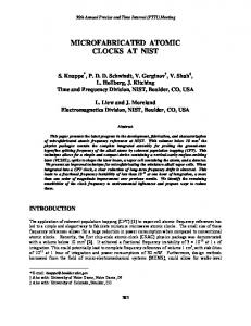
2 Microfabricated Vapour Cells The heart of the atomic clock physics package is a vapour cell containing a combination of alkali atoms and a buffer gas to reduce the wall-induced decoherence of the hyperfine oscillation. Vapour cells have traditionally been fabricated using conventional glass-blowing techniques, which have two important drawbacks. Firstly, it is difficult to make small cells because of the increasing importance of surface tension in shaping the melted glass at small sizes. Secondly, the cells must be made one by one, leading to substantial fabrication cost and difficulty integrating the cells with other clock components. We have developed a method of cell fabrication [5] based on techniques usually applied to microelectromechanical systems (MEMS). The cells are formed by sandwiching an etched Si wafer between two transparent glass wafers, as shown in Figure 1. A Si wafer, typically a few hundred micrometers thick, is lithographically patterned and etched by use of wetchemical (KOH) or deep-reactive-ion etching. An example of the wet-chemical etching process is outlined in Figure 2. By use of one of these processes, holes are etched through the wafer with a square cross-section of sides roughly 0.6 mm. However, the highly scalable nature of the etching process would allow holes as small as a few tens of microns to be created simply by changing the etch mask. Once the holes are created in the Si wafer, glass is attached to one side using the technique of anodic (or field-assisted) bonding [6]. Developed by Wallis and Pomerantz in 1969, this process can be used to bond flat wafers of borosilicate glass to a variety of materials including other glasses, metals
(Anodic bonding) +
silicon
Si wafer V
(b)
(a)
-
300 oC PyrexTM
-
(c)
LPCVD nitride deposition
Cesium + buffer gas
PR spin on V +
(d)
(f)
300 oC
PR exposure
(Anodic bonding) (e) Direct Injection Method
Chemical Reaction Method (Ba2N6 + CsCl)
Cs
N2 +
Bell-jar +
BaCl
heat Si
PyrexTM
Ultra High Vacuum Chamber (pressure = 10-6 Torr)
N2
pipette Cs
CF4 plasma h
Si PyrexTM
Anaerobic Chamber O22)) Anaerobic Chamber (< (0.0% 0.1 % O
PR strip
Figure 1 Schematic showing the steps in wafer-level fabrication of an alkali cell.
Anisotropic KOH etch
and Si. The bonding process is carried out by placing the two clean wafers in contact in a dust-free environment. The sample is then heated to approximately 300 ºC and a few hundred volts of potential difference is applied across the wafer pair (Figure 1c). Because of the high temperature, impurity ions in the glass (such as K+ and Na+) begin to drift in the electric field, leaving behind electrons. The electrons form a space-charge field, which attracts one material to the other and creates a strong bond between them. The bond is fully hermetic and ideal for confining alkali atoms inside the cell, as far as we have been able to ascertain.
Nitride strip
Once the initial piece of glass is bonded onto one side of the Si wafer, Cs (or Rb) is then deposited into the cell (Figure 1d and subpanels). This is carried out with one of two methods. The first method involves the chemical reaction of BaN6 and CsCl in a high-vacuum environment. These two materials are both soluble in water and are deposited into the cell preform in solution. The water is then evaporated and the preform, with remaining chemicals in solid form, is placed into a highvacuum chamber. The chamber is evacuated and backfilled with a buffer gas at an appropriate pressure. The sample is then heated to 150 ºC, at which point the chemicals react and create Cs, BaCl and N2. A second glass piece is then pushed up against the top of the sample, and the cell is heated further with an electric field applied to seal the Cs and buffer gas inside the cell. The residual N2 gas produced by the reaction presumably is pumped or diffuses away before the cell is sealed since the final buffer-gas pressure in the cell roughly matches the pressure in the chamber during bonding. The second technique of cell filling involves the use of an anaerobic chamber, essentially an airtight glove box with the water and oxygen reacted away. The cell preform is placed in the anaerobic chamber and Cs is added by breaking open a Cs ampoule inside the chamber and injecting some of the liquid metal using a micropipette. The cell preform is then placed inside a bell jar (inside the anaerobic chamber) that is
Figure 2 Steps to carry out anisotropic chemical etching of Si for cell fabrication. Silicon Nitride is deposited on a Si wafer using liquid-phase chemical vapour deposition (LPCVD). Photoresist (PR) is spun onto the nitride and exposed to ultra-violate (UV) light through a mask. The patterned PR and nitride is plasma-etched using CF4 and the PR is stripped off leaving the Si exposed. An anisotripic KOH etch is then used to etch holes in the exposed Si. Finally the nitride is removed. backfilled with the desired buffer gas. The second window is then attached, again using anodic bonding. After the final bonding step, the cells can be diced into individual components. A cell fabricated using the first method described above is shown in Figure 3. It should be clear that the process outlined in could be easily implemented at the wafer level. Lithographic patterning, etching and bonding of entire wafers are routinely done in the MEMS field and cell filling could be carried out either with an automated Cs dispenser (anaerobic chamber technique) or simultaneous deposition of chemical solution (chemical reaction technique).
3 Physics Package Design The development of wafer-level processing of planar cells allows for marked change in the design of frequencyreference physics packages. For the first time it becomes possible to assemble physics packages in an integrated, vertically-stacked structure. This type of structure allows not only for extremely small size but also for a corresponding reduction in power dissipation. In addition, this assembly method has the potential to drastically reduce the cost of manufacturing physics packages.
6P3/2
1.2 mm
852 nm
(a)
Normalized Transmitted Optical Power
1.0
F=4, mF=0
0.8
6S1/2
9.192 GHz
0.6
F=3, mF=0
0.4
(a)
0.2 0.0 -20
-10
0
10
20
Optical Frequency Detuning (GHz)
(b) Figure 3 (a) Photograph of a micromachined Cs vapour cell fabricated by anodic bonding. (b) Optical absorption resonance indicating the presence of Cs in the cell, along with approximately 250 Torr of buffer gas. The frequency references we are developing are based on the microwave transition between the F=3, mF=0 and F=4, mF=0 hyperfine sublevels of the 6S1/2 ground state of 133Cs. A coherence between these two levels can be generated through the phenomenon of coherent population trapping (CPT) [7,8,9] in a Λ-system (see Figure 4a). The CPT resonance is excited using light from a diode laser modulated through the injection current at one-half the Cs hyperfine splitting of 9.192 GHz [10] (see Figure 4b). The two first-order sidebands on the optical spectrum therefore create a Λ-system with the atoms on the D2 optical transition at 852 nm. When the laser modulation frequency is scanned near the first subharmonic of the hyperfine splitting, a resonance is observed by monitoring the total transmitted power through the cell with a Si PIN photodiode. This signal is used to determine when the local oscillator (LO) is on-resonance with the atoms. A schematic of one possible design of a fully integrated physics package is shown in Figure 5. A die containing a vertical-cavity surface-emitting laser (VCSEL) is bonded onto a substrate patterned with gold (Figure 5, layer a). The VCSEL is used because of its low power requirements (typically < 5 mW for most devices), high modulation efficiency and availability of single-mode devices at the 852 nm D2 transition in Cs. The light emitted by the VCSEL is conditioned by an optics assembly (Figure 5, layers b-f) attached to the baseplate. This optics assembly attenuates and collimates the light and change the light polarization from linear to circular. The cell assembly (Figure 5, layers g-k) is
Cell
VCSEL Local Oscillator
(b)
Photodiode
Figure 4 (a) Part of the Cs atom level spectrum showing the states relevant for CPT excitation. (b) Schematic of the experimental implementation based on a modulated diode laser. placed on top of the optics assembly. Because of the small optical path length in the cell, a temperature of about 80 ºC is required to provide an optimal signal. One way to accomplish this is to attach integrated heaters and temperature sensors to the cell structure. Finally a photodiode assembly (Figure 5, layers l-m) is mounted onto the top of the structure to detect the light power transmitted through the cell. An example of how physics packages might be assembled at the wafer level is shown in Figure 6. Power dissipation is a critical aspect of any design of a portable atomic frequency reference. A typical AA battery yields about 2000 mW-hours of power and therefore a few tens of milliwatts would be a reasonable goal for the power dissipation of a portable, battery-operated atomic clock. This is a challenging target since the cell must be held at a temperature several tens of Celsius degrees above ambient.
The power dissipation is in fact the primary consideration in determining how big the structure can be; larger cells radiate and conduct more power for a given temperature difference between the cell and the surroundings.
m
Despite the drawback of high cell temperature with regard to power dissipation, one rather fortuitous circumstance resulting from the small cell size is that the cell is operated above the range of temperatures typically specified for commercial devices. The cell must be actively temperature stabilized in order achieve good long-term frequency stability, and the high cell temperature obviates the need for a cooling mechanism, which is typically far less efficient than heating. As a result the small size of the cell is compatible with lowpower temperature stabilization.
l k j i h g f e
For the design in Figure 5, in which the cell is heated independently from the baseplate, the major heat loss channels are conduction through the cell support structure and electrical connections, conduction and convection through the air surrounding the structure, and radiation. Conduction through the air can be largely eliminated by packaging the structure in a vacuum enclosure. The power dissipated by radiation is given by (1) Q& rad = ασ (T14 − T04 )A ,
d c b
a
Figure 5: Schematic of one possible design of a microfabricated atomic clock physics package. Layer a is the laser, layers b-f are the optics assembly, layers g-k is the cell assembly and layers l-m are the photodiode assembly.
Photodiodes + Baseplate Spacer Heaters Cell Assemblies Heaters Waveplate Spacer ND Filter + Lenses Spacer Lasers + Baseplate
Figure 6 Wafer-level assembly of microfabricated frequencyreference physics packages.
where α is the surface emissivity, σ is the Stefan-Boltzmann constant, T1 is the cell temperature, T0 is the ambient temperature and A is the surface area of the device. If the interior of the vacuum enclosure were coated with a material such as gold, which has a radiative emissivity of about 0.02, the radiated power would be approximately 0.4 mW for T1-T0 = 100 K. Conduction through the support structure is perhaps the most important source of power dissipation. In the design shown in Figure 5, the cell is held away from the baseplate by two thin supports of rectangular cross section, As and height L. The power conducted through a support is given by A (2) Q& cond = I (T1 − T0 ) s , L where I is the thermal conductivity of the material. Polymer photoresist materials such as SU-8 have low thermal conductivity (about 0.2 W/(m·K)) and are also micromachinable. For supports 1.5 mm long, 0.1 mm wide and 0.5 mm high, the power dissipated to maintain temperature difference of 100 K is 12 mW. Conduction through the electrical connections can be minimized by making them thin and long. A gold trace 2 µm high, 50 µm wide and 2 mm long would dissipate only about 2 mW to support a temperature difference of 100 K between its ends. Since the laser wavelength depends on the temperature of the device, the laser temperature is typically actively stabilized. This requires power to heat the laser but because of the small size of the laser die, this power is substantially smaller than that required to heat the cell. The contact area of the laser on the baseplate is about 0.1 mm2. If the laser were mounted on a
thermally insulating polymer substrate, roughly 6 mW would be required to heat the laser to 100 K above ambient. Nonthermal sources of power dissipation within the physics package include the laser operation (< 5 mW), RF modulation (typically hundreds of microwatts) and detector bias (very small). Overall, therefore, it appears that a power dissipation of the order of tens of milliwatts is possible with this compact clock design. A summary of the physics package power budget is shown in Table 1. Table 1 Summary of power budget of physics package. Source Cell heating (∆T = 100 K) Laser heating (∆T = 100 K) Laser DC Laser RF Total
Power (mW) 20 6 4 0.1 30.1
[15]. Both of these technologies can be used to achieve high Q-factors (> 1000) at gigahertz frequencies and can be excited with low circulating power levels. The control electronics carry out the servo systems required to keep the system locked and stable. In the large-scale CPT frequency references currently operating in our laboratory, four servo systems are required. Two of these are temperature servos that stabilize the laser and cell temperatures. The remaining two are lock-in-based servos that stabilize the laser frequency onto the optical transition and the LO frequency onto the microwave transition. We anticipate that a microprocessor-based digital servo system would be appropriate for the frequency reference control. An alternative would be an application-specific integrated circuit (ASIC) in which an analogue circuit was implemented. The power required to run the local oscillator and control circuitry has not been evaluated with a high degree of certainty but levels in the range of tens of milliwatts are not out of the realm of possibility.
4 Anticipated Short-Term Frequency Instability The short-term instability of vapour-cell atomic frequency references is determined by a number of factors. Perhaps the most important is the resonance linewidth, which depends on both the frequency of collisions of the alkali atoms with the walls of the cell and also the pressure of the buffer gas used to prevent frequent wall collisions. Theoretical estimates based on diffusion in a buffer gas and complete depolarization on wall collisions indicate that a linewidth of near 1 kHz should be possible in a cell with dimensions of about 1 mm [11]. Experimental measurements confirm these predictions [12]. A second important factor is the resonance contrast, which we define as the ratio of the change in power due to the CPT resonance to the total absorbed power. For excitation on the D1 line of Rb, contrast values above 10 % have been observed [13]. Finally, the noise on the measured signal is determined fundamentally by the photon shot noise. For one microampere of detected photocurrent, the signal-to-noise ratio should be approximately 1 × 10⁵, assuming a contrast of 10 % and an absorption of 50 %. This leads to a fundamental short-term fractional frequency instability of roughly 1 × 10-12 at one second of integration. Real devices are expected to fall short of this mark due to technical noise and additional linewidth-broadening mechanisms such as power broadening and spin-exchange broadening, but this analysis nevertheless gives an indication of what might be possible in a millimeterscale device. Based on these numbers, a long-term instability below 1 × 10-11 should be easily achievable.
5 Integration With Other Components In addition to the physics package, two other components are required to enable a fully functional atomic frequency reference: a local oscillator and a control system. The local oscillator provides the initial (unstable) RF signal that is locked to the atomic resonance. Leading candidates to realize a compact, low-power local oscillator are thin-film bulkacoustic wave resonators [14] and SiC-based nanoresonators
6 Conclusions We have described here a fundamentally new design for compact atomic frequency references based on MEMS microfabrication techniques. Advantages of this technique include small size, low power dissipation, low-cost massproduction through wafer-level processing and a high degree of scalability. These features may enable atomic frequency references to be integrated into portable, battery-operated devices used for global positioning and wireless data communications.
Acknowledgements This work is supported by NIST and the Defence Advanced Research Projects Agency (DARPA). This work is a contribution of NIST, an agency of the US government, and is not subject to copyright.
References [1]
P. J. Chantry et al., “Miniature laser-pumped cesium cell atomic clock oscillator,” Proc. 1996 IEEE Int. Freq. Cont. Symp, 1002-1010 (1996). [2] J. Ho, I. Pascaru, C. Stone and T. McClelland, “New Rubidium frequency standard designs for telecommunications applications,” Proc. 1998 IEEE Int. Freq. Cont. Symp, 80-83 (1998). [3] H. Fruehoff, “Fast “direct-P(Y)” GPS signal acquisition using a special portable clock,” Proc. 33rd Ann. Precise Time and Time Interval (PTTI) Meeting, pp. 359-369 (2001). [4] S. Knappe, L. Liew, V. Shah, P. Schwindt, J. Moreland, L. Hollberg and J. Kitching, “A micromachined atomic clock,” to be published.
[5] L. Liew, S. Knappe, J. Moreland, H. G. Robinson, L. Hollberg and J. Kitching, “Micromachinined alkali atom vapor cells,” Appl. Phys. Lett. 84, 2694-2696 (2004). [6] G. Wallis and D. I. Pomerantz, “Field assisted glassmetal sealing,” J. Appl. Phys. 40, 3946-3949 (1969). [7] W. E. Bell, A. L. Bloom, “Optically driven spin precession,” Phys. Rev. Lett. 6, 280-281 (1961). [8] G. Alzetta, A. Gozzini, L. Moi, G. Orriols, “An experimental method for the observation of R. F. transitions and laser beat resonance in oriented Na vapor,” Il Nuovo Cim. 36B, 5-20 (1976). [9] E. Arimondo, “Coherent population trapping in laser spectroscopy,” Progress in Optics XXXV, E. Wolf, ed., 257-354 (1996). [10] J. Kitching, S. Knappe, N. Vukicevic, L. Hollberg, R. Wynands, and W. Weideman, “A microwave frequency reference based on VCSEL-driven dark line resonances in Cs vapor,” IEEE Trans. Instrum. Meas. 49, 13131317 (2000). [11] J. Kitching, S. Knappe and L. Hollberg, “Miniature vapor-cell atomic frequency references,”Appl. Phys. Lett. 81, 553-555 (2002). [12] S. Knappe, L. Hollberg and J. Kitching, “Dark-line atomic resonances in sub-millimeter structures,” Opt. Lett. 29, 388-390 (2004). [13] M. Stahler et al., “Coherent Population Trapping Resonance in a Thermal 85Rb vapor: D1 versus D2 line excitation,” Opt. Lett., 27, 1472-1474 (2002). [14] K. M. Lakin, J. S. Wang, “Acoustic bulk wave composite resonators,” Appl. Phys. Lett. 38, 125-127 (1981). [15] X. M. H. Huang, C. Zorman, M. Mehregany, M. L. Roukes, “Nanodevice motion at microwave frequencies,” Nature 421, 496 (2003).