Modeling of the electron field emission process in polycrystalline diamond and diamond-like carbon thin films S. R. P. Silvaa) School of Electronic Engineering, University of Surrey, Guildford, Surrey GU2 5XH, England
G. A. J. Amaratunga Department of Engineering, University of Cambridge, Cambridge CB2 1PZ, England
K. Okano Department of Physics, International Christian University, Tokyo, Japan
~Received 19 July 1998; accepted 28 January 1999! Electron field emission has been observed from carbon thin films at relatively low electric fields. These films range from amorphous carbon to polycrystalline diamond films. There are many models that attempt to account for the electron field emission process observed in these films. The initial models that were based on the emission due purely to a negative electron affinity have now been modified. The emission from diamond like carbon ~DLC! films, although following a Fowler– Nordheim type curve, do not give realistic values for the emission areas or barriers purely based on a tunneling mechanism. Therefore, a model based on space charge band bending at the back junction is proposed to account for the electron emission at low electric fields from DLC. In this ‘‘space charge interlayer’’ model the real cathode is the substrate, from which hot electrons are created due to the fully depleted DLC film the electrons encounter before reaching the front surface of the film. In this article we extend the model to incorporate the emission of electrons from polycrystalline diamond thin films. © 1999 American Vacuum Society. @S0734-211X~99!10802-3#
I. INTRODUCTION Research into the next generation of display technologies that are flat and cheap to manufacture has produced a number of contenders. The liquid crystal display ~LCD! is the clear market leader at present, with flat panel displays ~FPD! based on field emission processes being envisaged as a major contender for future high definition display applications such as televisions.1 In order for these field emission based flat panel displays to operate commercially, stable long lasting cathodes that do not degrade with time are needed over large areas. Chemical vapor deposition based systems are well suited to produce large area thin films at relatively low cost. Current FPDs based on field emission utilize metal tips ~such as Mo! in order to create field enhancement at their tips to extract electrons. The lifetime of the cathodes and the relative expense incurred in the integrated electronic driver circuitry used for FPDs can be vastly improved if the voltages, and thus the electric fields, that need to be switched to extract electrons from the cathode were to be lowered. To lower the electric field required to extract electrons from the cathode, the emission process needs to be understood and suitable materials once identified, modeled. Diamond thin films have been proposed as a viable cold cathode alternative for field emission applications due to the apparently low ~or negative! electron affinity making it feasible for use as flat cathodes that operate at low electric fields. A number of research groups have shown experimental results in which the electron emission from polycrystalline diamond and diamond like carbon ~DLC! ~or amorphous carbon! has been a!
Corresponding author; electronic mail:
[email protected]
557
J. Vac. Sci. Technol. B 17„2…, Mar/Apr 1999
achieved at low threshold fields.2–7 In this article we will develop a model that can be used to explain the observed electron emission characteristics of polycrystalline diamond using a model which involves the presence of DLC ~or amorphous carbon! at/in the grain boundaries. Carbon and carbon based alloys were initially pursued as possible electron emitters due to diamond having a negative electron affinity on certain crystalline planes when terminated with hydrogen.8 Models based purely on the electron affinity have been postulated in the past. We present a model in this article for electron emission due to space charge induced band bending creating hot electrons which gain energy to exit its host material ~‘‘interlayer’’! by virtue of its fully depleted bands.9–11 If this model is correct, it is expected that not only DLC or amorphous carbon ~a-C! but other materials with low electron affinities ~in the range 2–3 eV! would also be suitable to act as space charge interlayers for the release of electrons from highly doped substrates into vacuum.12–14
II. FIELD ELECTRON EMISSION MODELS FOUND IN THE LITERATURE In the case of field electron emission from thin films, there are three aspects that need to be examined when modeling electron emission, namely, the electron source, the injection/transport of electrons within the source, and the release mechanism of electrons into vacuum. In the case of models based on negative electron affinity ~NEA! cathodes, an electron source is required to ‘‘pump’’ electrons into the conduction band of the NEA material, from which there is
0734-211X/99/17„2…/557/5/$15.00
©1999 American Vacuum Society
557
558
Silva, Amaratunga, and Okano: Modeling of the electron field emission process
only a small barrier, due to surface effects such as dipoles, that needs to be overcome for electron emission to take place. Bayliss and Latham15 proposed a hot electron emission model based on band bending from wide band gap insulating material. A phenomenological model for field emission from nitrogen containing hydrogenated amorphous carbon ~aC:H:N! using a semiconductor model with space charge band bending induced hot electrons has also been proposed.9 Additional results have shown that the ‘‘interlayer’’ model may be extended to explain electron emission from other amorphous materials such as tetrahedral a-C ~ta-C!,12 amorphous silicon carbide ~a-SiC!,13 and amorphous silicon ~a-Si!.14 The question that should be paramount in considering emission from diamond and polycrystalline diamond films is where the source of the electrons that are emitted to the surface originates. We know that diamond is a large band gap semiconductor with an optical gap of 5.5 eV. It is also well known that it is difficult to electronically dope polycrystalline diamond films n type. Therefore, even though diamond has a negative electron affinity ~or low positive electron affinity! on certain crystal planes, it has a very low intrinsic concentration of electrons in the conduction band, as with most wide gap semiconductors/insulators that cannot be electronically doped n type. On the other hand, field emission results on all polycrystalline diamond samples clearly show field emission at relatively low electric fields. The results of Zhu et al.2 show the more defective the polycrystalline diamond @observed by the full-width at half-maximum ~FWHM! of the Raman signal# to lower the electric field required for electron field emission. Similar results have also been observed by others.3 Zhu et al.2 have explained this behavior using a model in which additional defect subbands are created within the 5.5 eV band gap of diamond. Other models introduced include the electron emission in diamond via graphite inclusions which act as conducting regions which help induce higher electric fields in the interior of the diamond and models which discuss the possibility of enhanced conductivity along grain boundaries.16 An alternative model in which emission occurs via surface states located ;1 eV below the conduction band of diamond was proposed17 based on theoretical calculations. The problem of how a continuous source of electrons may be supplied from a back contact into the conduction band of the diamond at a relatively low electric field has been a complex issue not answered satisfactorily as of yet. It is very unlikely that electrons will be thermally excited directly into the conduction band of diamond to supply the measured emission current from states situated 4 eV below it at the reported low threshold fields. Values below 5 V/mm have been observed by a number of groups. Assuming there is field penetration into the diamond films, which may be unlikely due to the large thickness ~tens of microns! of some films, then due to the dielectric constant of 5.5 of diamond, Gauss’ law gives an electric field of less than 1 V/mm in the semi-insulating films which is insufficient to induce enough J. Vac. Sci. Technol. B, Vol. 17, No. 2, Mar/Apr 1999
558
band bending to surmount most barriers ~especially the large barrier at the back contact!. Therefore, although having a negative electron affinity or low positive affinity is of importance in the final stage of electron emission into vacuum, a source of electrons that maintain the conditions for current continuity must also be present. Geis et al.18,19 noted the importance of the back metal contact in their type Ib n-type diamond. They found that once a threshold voltage of several kV was applied across their substrates, an electric field of only ;0.2 V mm21 was required for emission to take place. The applied voltage for emission was approximately independent of anode-cathode spacing. But, in the case of the boron doped p-type diamond an electric field of 24 V mm21 was required for emission to take place. They18,19 also showed that by varying the surface roughness of their back contact it was possible to vary the electric field required for field emission to take place. This was attributed to the rougher back contact, which made it more likely for electrons to enter the conduction band of the diamond films by tunneling due to the high local fields. It is of course possible that with the roughening of the back surface, a more pronounced DLC interface layer will come into existence and thereby help improve the emission properties not only by increasing the b value but also due to space charge band bending as discussed in this model. These experiments emphasize the importance of the back contact, and indicate that the rate limiting process for electron emission may also be associated with it. III. SPACE CHARGE INTERLAYER MODEL FOR POLYCRYSTALLINE DIAMOND In the model by Amaratunga and Silva,9 a fully depleted, doped interlayer is shown to sustain a larger electric field than the applied macroscopic field due to space charge effects as a consequence of having to satisfy the Poisson relationship in the interlayer. The highly doped n 11 -Si and a-C:H:N film acts as a heterojunction and using the electron affinity value calculated by Robertson20 of ;2.5 eV for the DLC ~a-C! film a large band discontinuity is predicted at this junction. It has been shown by high resolution scanning tunneling electron microscopy coupled with electron energy loss spectroscopy that polycrystalline diamond grains are surrounded by a thin layer of amorphous carbon.21 This result has been confirmed by micro-Raman analysis across grain boundaries22 and very recent electron energy-loss spectra ~EELS! analysis that has examined the joint density of states ~JDOS! of polycrystalline diamond.23 A schematic of the polycrystalline diamond based on these results is shown in Fig. 1. In the context of electron field emission from polycrystalline diamond this is of crucial importance in that by having such a layer of DLC ~or a-C! at the back contact it is probable that space charge based band bending can arise. This means that when the DLC is fully depleted, electrons at relatively low electric fields can become ‘‘hot’’ by drifting down the DLC and enter the conduction band of the diamond. Once in the diamond conduction band they can be
559
Silva, Amaratunga, and Okano: Modeling of the electron field emission process
559
FIG. 1. Cross-sectional and plan view schematics of the polycrystalline diamond thin films. The thicker bold lines indicate grain boundaries at which amorphous carbon is present. These figures are based on the work by Fallon and Brown ~Ref. 24!.
readily emitted at low fields due to the low electron affinity of the diamond surface. In the phenomenological model proposed, for the most basic case a structure composed of a metal or highly doped Si substrate will be followed by the DLC layer ~grain boundary! with a crystalline diamond front surface, as shown by the band diagrams in Figs. 2 and 3. Therefore, there are two barriers observed by electrons prior to emission for this simple case, one between the metal ~or Si! and the DLC ~a-C!, and the other between the DLC ~a-C! and the polycrystalline diamond. Due to the amorphous na-
FIG. 3. Proposed electronic band diagram for field emission from p-type polycrystalline diamond films. ~a! At equilibrium and ~b! under an applied electric field.
FIG. 2. Proposed electronic band diagram for field emission from n-type polycrystalline diamond films; ~a! at equilibrium with no applied field, and ~b! under a moderate electric field. An n-doped amorphous carbon thin film surrounds the diamond grains. JVST B - Microelectronics and Nanometer Structures
ture of the grain boundaries it is quite possible that instead of two barriers there could be multiple barrier components associated in a mixed sp 3 /sp 2 phase material.24 Assuming a typical value for the DLC grain boundary thickness of 10–20 nm,21 and an active nitrogen dopant concentration of say 531018 cm23 (;331020 cm23 was measured as the N content7! in the n-doped diamond films discussed here, values between 1 and 5 V are calculated for the potential drop in the space charge induced fully depleted DLC layer purely based on the solution to Poisson’s equation. In this calculation, an electron affinity and mobility gap of 2.5 and 2.0 eV have been assumed for the DLC in the grain boundaries.9 The DLC ~a-C! films too have been taken to be doped due to the dopants present in the polycrystalline diamond films being intermixed in the thin amorphous films ~Figs. 2 and 3!. The ‘‘blocking back contact’’ is essential for hot electron emission from the fully depleted interlayer ~DLC! in that it allows for only the more energetic electrons to drift through the semiconductor and gain energy by heating to move into the conduction band of the diamond. Electrons that do not gain enough energy to move into the conduction band of the diamond in the first attempt will give rise to accumulation of the electrons in the conduction band of the DLC ;1.5 eV below the conduction band of the diamond ~for both cases!. These may subsequently gain energy from
560
Silva, Amaratunga, and Okano: Modeling of the electron field emission process
560
opposed to the abrupt 4 eV metal ~or Si!-diamond back contact without a DLC transition layer. IV. DISCUSSION
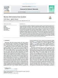
FIG. 4. Electron field emission from doped polycrystalline diamond thin films ~Ref. 7!.
incoming ‘‘hot’’ electrons to move to higher levels and ultimately reach the vacuum via the conduction band of the diamond film. The band diagram of equilibrium, with no applied electric field, for the polycrystalline DLC films assuming an amorphous DLC ~a-C! boundary layer at the back of each crystal is shown in Figs. 2~a! and 3~a! for the n- and p-doped diamond films, respectively. The diamond is assumed to have an electron affinity of ;0.5 eV, with the metal giving a typical known Schottky barrier height f sb close to 4 eV for the diamond being used as the back contact.20 In Fig. 2, the n-type diamond which is assumed to be doped with N, has an activation energy of 1.7 eV with respect to the conduction band and the p-type diamond in Fig. 3 is assumed to have an activation energy of 0.3 eV with respect to its valence band. The figures are to illustrate quantitatively on how a thin layer of DLC ~a-C! at a grain boundary in polycrystalline diamond will help in the emission of electrons at relatively low threshold fields. A more detailed analysis of the band bending observed, without consideration of the DLC interfacial layer, can be found in the work of Lerner et al.25 who clearly show the band bending due to space charge for the n-Si/n-doped diamond film when the current continuity equation is solved rigorously for the whole system. It is quite encouraging that this phenomenological model using the space charge analysis gives rise to band diagrams similar to those obtained by Lerner.25 It is interesting to note that the band diagrams constructed according to our model, an n-doped polycrystalline diamond film would need a significantly lower threshold field for emission in comparison to a p-doped film. This is observed in the results of Geis et al.19 and the results obtained in this study shown in Fig. 4. Figure 3~b! shows the p-type diamond after a rather high field has been applied @in comparison to n-doped Fig. 2~b!# and the bands now have a shallow negative gradient. Under zero bias conditions, Fig. 3~a!, high positive gradient results. The figures clearly illustrate that it is easier for electrons to surmount a two stage barrier as J. Vac. Sci. Technol. B, Vol. 17, No. 2, Mar/Apr 1999
The above analysis may be used to explain the results observed by Zhu et al.2 and Wistsora et al.3 where the higher the amorphous component in their polycrystalline diamond films, the lower the threshold electric field that was required to emit electrons. On the basis of our model we would see this as being due to an increase in the DLC containing grain boundaries across which the electrons could travel and gain energy. A small energy gain of the electrons by heating due to drift in an electric field in the DLC film is sufficient to overcome the surface barriers shown in the figures. The DLC in the diamond grain boundaries effectively acts as a stepping stone for the emission of electrons by providing a two ~or multi! stage process for the gaining of energy.24 Although it is possible for the electrons to be directly emitted to the vacuum from the DLC ~grain boundaries! if it were to gain sufficient energy, it would have to overcome a significantly larger surface barrier in comparison to if it were to use the two or multistage process. Therefore, it is more probable that the emission will be via the diamond surface rather than the grain boundaries. The observations of Geis et al.18 may also be explained using the above model. In the case of the type Ib nitrogen doped diamond; once the electrons have enough energy to overcome the two barriers, little or no further field is required due to the band bending in the n-diamond films which will readily emit electrons. Therefore, the apparent independence of the threshold voltage to anode-cathode spacing in the results is reported. In the case of the p-diamond films, even though electrons may be excited to the conduction band of diamond at the DLC p-diamond interface, due to the nature of the initial band bending a higher applied voltage will be required as the flat band condition has to be reached before carriers can tunnel into the diamond from the DLC and be transported to the surface for emission18 @Fig. 3~b!#. The voltage which has to be maintained between the emitting surface of diamond and the back contact is significantly higher in this case, and will be seen as a larger rise in the anode-cathode field required for electron emission. A number of models have been introduced that discuss the space charge effects in the interlayer material and junctions.6,18,19,25–27 Hot electrons caused by space charge induced band bending have also been proposed as a possible mechanism by which electrons are emitted from polycrystalline diamond deposited on metal tips.6 But, yet in all these cases,6,18,19,25–27 the space charge region has been confined to within the crystalline diamond. In the work by Geis et al.18,19 and Lerner et al.25,26 a small layer of the diamond back surface is assumed to be ionized due to asperities at the back contact. Reference 6 discusses emission from metal tips, which have a diamond crystal on its apex, which discusses a similar process to the Geis and Lerner emission processes. We in our model for the first time have introduced the concept of fully depleted grain boundaries giving rise to the
561
Silva, Amaratunga, and Okano: Modeling of the electron field emission process
observed field emission results in doped and undoped polycrystalline DLC films. The grain boundaries being thin enough to not only be fully depleted when a suitably large electric field is applied to the cathodes, but also be able to sustain a sufficient voltage drop to give rise to the ‘‘heating’’ of electrons within a short spatial distance. It is interesting to note that recent field electron energy distribution ~FEED! experiments by Schlesser et al.28 indicate the presence of space charge in the diamond films, and according to their results an applied macroscopic field of 2 V/mm created an electric field greater than 10 V/mm within the diamond film. In the proposed space charge interlayer model such a result is expected. The data shown in Fig. 4 for doped diamond films further strengthens the arguments for an interlayer model by showing that n-type materials, namely nitrogen and phosphorus doped films give significantly better results than the boron doped p-diamond films. It should be noted that although phosphorous is a shallow donor in comparison to nitrogen in the polycrystalline diamond films, the nitrogen level may be more advantageously situated for band bending and depletion of the DLC layers. It is well known that with increased impurity addition in diamond, more sp 2 states are created which could also help in the creation of more uniform regions of grain boundaries that can help with the electron emission process. In conclusion, a space charge induced hot electron model is proposed to explain the observed electron emission characteristics of diamond and diamond-like carbon thin films. The phenomenological model proposed in this article may be extended to other amorphous and polycrystalline semiconducting materials. K. Derbyshire, Solid State Technol. Nov., 55 ~1994!; J. Jaskie, MRS Bull. 21, 59 ~1996!. 2 W. Zhu, G. P. Kockanski, S. Lin, and L. Siebels, J. Appl. Phys. 78, 2707 ~1995!. 3 A. Wisitsora-at, W. P. Kang, J. L. Davidson, and D. V. Kerns, Appl. Phys. Lett. 71, 3394 ~1997!. 4 W. S. Xu, Y. Tzeng, and R. V. Latham, J. Phys. D 26, 1776 ~1993!. 5 M. W. Geis, J. A. Gregory, and B. B. Pate, IEEE Trans. Electron Devices 38, 619 ~1991!. 1
JVST B - Microelectronics and Nanometer Structures
6
561
E. I. Givargizov, V. V. Zhimov, A. V. Kunznetsov, and P. S. Plekhanov, J. Vac. Sci. Technol. B 14, 2030 ~1996!. 7 K. Okano, S. Koizumi, S. R. P. Silva, and G. A. J. Amaratunga, Nature ~London! 381, 140 ~1996!. 8 F. J. Himpsel, J. A. Knapp, J. A. Van Vechten, and D. E. Eastman, Phys. Rev. B 20, 625 ~1979!; B. B. Pate, Surf. Sci. 165, 83 ~1986!. 9 G. A. J. Amaratunga and S. R. P. Silva, Appl. Phys. Lett. 68, 2529 ~1996!. 10 S. R. P. Silva, R. D. Forrest, D. A. I. Munindradasa, and G. A. J. Amaratunga, Diamond Relat. Mater. 7, 645 ~1998!. 11 R. D. Forrest, A. P. Burden, S. R. P. Silva, L. K. Cheah, and X. Shi, Appl. Phys. Lett. 73, 3784 ~1998!. 12 L. K. Cheah, X. Shi, B. K. Tay, S. R. P. Silva, and Z. Sun, Diamond Relat. Mater. 7, 640 ~1998!. 13 S. R. P. Silva et al., in Proceedings of the First Specialist Meeting on Amorphous Carbon, edited by S. R. P. Silva, J. Robertson, W. I. Milne, and G. A. J. Amaratunga ~World Scientific, Singapore, 1998!, pp. 350– 361. 14 S. R. P. Silva, R. D. Forrest, and J. M. Shannon, J. Non-Cryst. Solids 227–230, 1101 ~1998!. 15 K. H. Bayliss and R. V. Latham, Proc. R. Soc. London, Ser. A 403, 285 ~1986!. 16 C. Wang, A. Garcia, D. C. Ingram, and M. E. Kordesh, Electron. Lett. 27, 1459 ~1991!. 17 Z. Huang, P. H. Cutler, N. M. Miskovsky, and T. E. Sullivan, Appl. Phys. Lett. 65, 2562 ~1994!. 18 M. W. Geiss, J. C. Twitchell, and T. M. Lyszczarz, J. Vac. Sci. Technol. B 14, 2060 ~1996!. 19 M. W. Geis, J. C. Twitchell, N. N. Efremow, K. Krohn, and T. M. Lyszczarz, Appl. Phys. Lett. 68, 2294 ~1996!. 20 J. Robertson and W. I. Milne, J. Non-Cryst. Solids 227–230, 558 ~1998!. 21 P. J. Fallon and L. M. Brown, Diamond Relat. Mater. 2, 1004 ~1993!. 22 N. Kikuchi, T. Komatsu, and H. Yamashita, Proceedings of the 10th Symposium On Ion Sources and Ion Assisted Technology, Tokyo, 1986, ISIAT Foundation, Tokyo ~unpublished!, p. 359. 23 G. A. J. Amaratunga, A. P. Papworth, and C. J. Kiely, Institute of Physics Meeting, London, 22 September 1998. 24 X. Shi, L. K. Cheah, B. K. Tay, and S. R. P. Silva, Appl. Phys. Lett. 74, 833 ~1999!. 25 P. Lerner, N. M. Miskovsky, and P. H. Cutler, J. Vac. Sci. Technol. B 16, 900 ~1998!. 26 P. Lerner, P. H. Cutler, and N. M. Miskovsky, J. Phys. IV C5 6, 39 ~1996!. 27 H. J. Fitting, Th. Hingst, E. Schreiber, and E. Geib, J. Vac. Sci. Technol. B 14, 2087 ~1996!. 28 R. Schlesser, M. T. McClure, W. B. Choi, J. J. Hren, and Z. Sitar, Appl. Phys. Lett. 70, 1596 ~1997!.