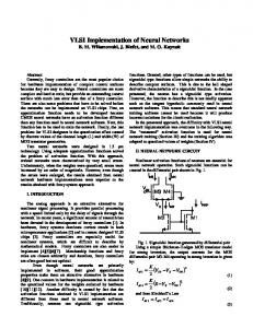
important that the data is checked for sanity by 2-D or 3-D plotting. AC1IULDMCLon. PROCESS SPCCS-. WRUALUATDll. POST-NEURAL. CODE ENHANCING.
SIMULATION OF SEMICONDUCTOR DEVICES A N D PROCESSES Vol. 5 Edited by S. Selberherr, H. Stippel, E. Strasser - September 1993
Modeling of VLSI MOSFET Characteristics Using Neural Networks Ph. Lindorfer and C. Bulucea National Semiconductor Corporation 2900 Semiconductor Dr., Santa Clara, CA 95052, USA
Abstract Neural modeling of transistor current-voltage characteristics is explored as a possible solution to the complexity and accuracy problems currently encountered with analytical representations of VLSI devices. The neural modeling methodology is discussed along with first results obtained for a 0.8 pm CMOS process. The drain and substrate current-voltage characteristics of an n-channel MOSFET device are modeled over a drain current range of 10 orders of magnitude, from deep subthreshold to high-current operation.
1. Introduction The compact MOSFET models for circuit simulation are customarily built around the parabolic approximation derived in the classical long-channel theory. While this approach is adequate for channel lengths larger than 2 pm, it tends to lead to excessively complicated parameter definitions when modified for submicron devices. Moreover, the good match between models and experimental data reported for particular processes fails to yield similar results on different processes. This explains the quite respectable size of the compact modeling literature, as well as the continuous demand for more accurate modeling coming from circuit designers. To cope with the increasing complexity of the state-of-the-art VLSI scenario, we propose the more pragmatic approach of representing the transistor as a computersimulated neural network, the connection strengths (or weights) of which are computed by training the network on measured or simulated data. The neural networks methodology is essentially used here as a convenient multi-variable, multi-function interpolation tool, rather than as a predictive tool, as usually reported. The basic terminology of neural networks, typed in italics, is assumed to be known, and the readers not yet exposed to it are referred to the introductory book [I] and to the representative selection of the classical neurocomputing papers [2].
2. Modeling Methodology with Neural Networks The principal steps of developing the neural network model of an electronic device are described in the flowchart of Fig. 1. The training and testing data are obtained from electrical measurements, or from numerical simulations, at a given input parameter
34
Ph. Lindorfer et al.: Modeling of VLSI MOSFET Characteristics Using Neural Networks
matrix. Since neural modeling does not involve any physics-based validation, it is important that the data is checked for sanity by 2-D or 3-D plotting. AC1IULDMCLon PROCESSSPCCS ~ -
WRUALUATDll
POST-NEURAL CODE ENHANCING
RULES
2
4
8
6
1
D r a l n Voltage, VD [ V ]
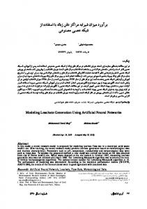
Fig. 1 - Simplified flowchart of the device modeling methodology based on neural networks. Fig. 2 - Drain I-V characteristics used for training: (a) actual (curves with circles), and normalization (straight lines) data at VG = 0, 1, 2, 3, 4, and 5 V, and (b) normalized dataat VG = 0, 0.4,0.8, 1, 1.5, 2, 3,4, and 5 V.
! 0
! 2
!
! 4
!
!
!
6
! 6
! 1
Draln Voltage, V D [V]
The neural network algorithms assume that the input and output values of the modeled system are scaled to finite linear ranges, such as from -1.0 to +1 .O, that are compatible with the transfer functions of the processing elements (or neurons) involved, and do not cause their saturation. This poses a prime difficulty to neural modeling of semiconductor devices, where the output currents vary by many orders of magnitude. Simple linear presentation of the actual data results, at best, in modeling the two uppermost decades of the output quantities. Conversely, simple logarithmic presentation compresses excessively the upper ranges, losing modeling accuracy there. To cope with this difficulty, adequate normalization functions have to be devised for each output quantity, such that the data are uniformly compressed to a linear range. Following normalization, the training data are fed into the neural simulator, together with the previously determined network type, structure and learning schedules. The neural simulation software repeatedly presents the data to the network and adjusts the connection weights using error minimization algorithms [3]. When a limit or a predetermined error for the output quantities is reached, the connection weights are set to their final values and, if tested satisfactorily, the network is able to model the device. A computer code is automatically generated for the normalized data, which is externally enhanced for denormalization and inclusion of device scaling rules.
Ph. Lindorfer et al.: Modeling of VLSI MOSFET Characteristics Using Neural Networks
3. Data Preparation for Neural Network Training The training data used for this study were generated using MINIMOS and VISTA [4], a Technology Computer-Aided Design environment, both from the Technical University of Vienna, using the process characteristics of the company's 0.8pm/5V CMOS process. The goal was t o model the DC characteristics of the drain and substrate currents as functions of the gate and drain voltages, such as to continuously cover the full gate voltage range, from subthreshold to high-current operation (0 to 5 V), and the drain voltage range from zero to incipient avalanche multiplication (0 t o 10 V). The substrate was biased to source potential. Fin. 2a illustrates the normalization Drocess for the drain current. where the linear reiion I-V characteristics at each = gch(VG) V; are used as norvoltage, IDN malization functions, with g c h ( V ~determined ) at VD = 0.1 V. To simplify training, a look-up table representation of the normalization function was preferred t o an analytical function. The normalized drain current ID/IDN used for training, plotted in Fig. 2b, has a reduced dynamic range, and varies monotonically with the gate voltage. The network was actually presented the logarithm of this ratio. A similar normalization scheme was used for the substrate current, where the substrate current determined at VD = 10 V was used as a normalization function, also in a look-up table representation as a function of Vc. A complete training set in this case consisted of 10 ordered data subsets at constant gate voltages, each having 22 drain voltage points.
4. Neural Network Architecture, Parameters, Results With the ultimate goal of modeling for VLSI design, the networks considered were extremely simple, in order to minimize the calculation time of circuit simulators. Different network architectures and learning strategies were tried, all of which were of the back-propagation type. The PC1386 version of the Neuralware Professional II/Plus [3] software was chosen, from several commercially available packages, due to its multiple options of neural paradigms and monitoring devices. The best results were obtained with networks having two hidden layers, the typical architecture being 2 * input (linear)
4...8
* hidden1 (tanh) + 3...4 * hidden2 (tanh) + 2 * output (tanh),
where the transfer function of the processing element is specified in parentheses. The Delta-Rule learning was generally preferred, with data presented sequentially. Fig. 3 shows a typical well behaving network around the beginning of the training process. The Summation Value instrument averages its values over a displaying epoch equal t o the number of sets (220) in the training file. The RMS Error instrument averages " the root mean sauare error of the o u t ~ u t sover the same ~ e r i o d .The arrows on the error curve mark the transition points of the learning schedule, where the learning coefficients are changed to avoid processing element saturation. The final value of the linear correlation coeficient of the desired and actual outputs, printed on the vertical axis of the confusion matrix (see Fig. 3), is 0.9989. High values of this coefficient, in the range reported here are required for accurate modeling.
36
Ph. Lindorfer et al.: Modeling of VLSI MOSFET Characteristics Using Neural Networks
Fig. 3 - Typical NeuralWare Professional II/Plus screen of a well behaving network, around the beginning of the training. Fig. 4 - Characteristics of a VLSI nchannel MOSFET: (a) real, and (b) modeled by a 2 + 6 + 4 + 2 network. VG= 0,0.4,0.8,1.0,1.5,2,3,4,5V.
Fig. 4 illustrates the results of this modeling experience, for the simple network represented in Fig. 3, comparing the real (a) and modeled (b) characteristics of the drain current over the full range of gate and drain voltages, covering ten orders of magnitude. The network yielded similar results for the substrate current. The modeling accuracy is quite surprising considering the relative simplicity of the network used.
5. Conclusions The neural representation is shown to be a practical and universally applicable modeling tool for accurate simulation of submicron VLSI devices. The vast variety of options available for neural modeling, ranging from fundamentally different network architectures and normalization functions, to details of training algorithms and schedules invite further communication exchange.
References [I] Jeannette Lawrence, Introduction to Neural Networks and Expert Systems, California Scientific Software, Nevada City CA, 1992. [2] James A. Anderson and Edward Rosenfeld, Neurocomputing: Foundations of Research, M I T Press, Cambridge MA, 1990. [3] NeuralWare Staff, Neural Computing - NeuralWorks Professional 11 /PLUS and NeuralWorks Explorer, Software User's Manual, NeuralWare Inc., Pittsburgh PA, 1991. [4] S. Halamaet al., Consistent User Interface and Task Level Architecture of a TCAD System, Proceedings NUPAD IV, Seattle WA, 1992.