Microprocessors and Microsystems (Elsevier journal), accepted for publication, 2015
Modular Vector Processor Architecture Targeting at Data-Level Parallelism Seyed A. Rooholamin and Sotirios G. Ziavras Department of Electrical and Computer Engineering New Jersey Institute of Technology Newark, NJ 07102, USA
[email protected] Abstract: Taking advantage of DLP (Data-Level Parallelism) is indispensable in most data streaming and multimedia applications. Several architectures have been proposed to improve both the performance and energy consumption for such applications. Superscalar and VLIW (Very Long Instruction Word) processors along with SIMD (Single-Instruction Multiple-Data) and vector processor (VP) accelerators, are among the available options for designers to accomplish their desired requirements. We present an innovative architecture for a VP which separates the path for performing data shuffle and memoryindexed accesses from the data path for executing other vector instructions that access the memory. This separation speeds up the most common memory access operations by avoiding extra delays and unnecessary stalls. In our lane-based VP design, each vector lane uses its own private memory to avoid any stalls during memory access instructions. The proposed VP, which is developed in VHDL and prototyped on an FPGA, serves as a coprocessor for one or more scalar cores. Benchmarking shows that our VP can achieve very high performance. For example, it achieves a larger than 1500-fold speedup in the color space converting benchmark compared to running the code on a scalar core. The inclusion of distributed data shuffle engines across vector lanes has a spectacular impact on the execution time, primarily for applications like FFT (Fast-Fourier Transform) that require large amounts of data shuffling. Compared to running the benchmark on a VP without the shuffle engines, the speedup is 5.92 and 7.33 for the 64-point FFT without and with compiler optimization, respectively. Compared to runs on the scalar core, the achieved speedups for this benchmark are 52.07 and 110.45 without and with compiler optimization, respectively. Keywords: Parallelism, vector processor, performance, speedup, benchmarking.
1. Introduction High-performance computing processors often have a superscalar or VLIW architecture that focuses mostly on exploiting ILP (Instruction-Level Parallelism). Roger et. al.[1] show that ILP and DLP can be merged in a single simultaneous vector multithreaded architecture for higher performance. VIRAM’s [2] basic multi-lane architecture can be used to build VPs that exploit DLP through SIMD processing. Each lane contains similar pipelined execution and load-store units. Each vector register is uniformly distributed among the lanes. All the elements from a vector in a lane are processed sequentially in its pipelined units while corresponding elements from different lanes are processed simultaneously. Using EEMBC benchmarks, it was demonstrated that a cache-less VIRAM is much faster than a superscalar RISC or a cache-based VLIW processor [3].
1
Microprocessors and Microsystems (Elsevier journal), accepted for publication, 2015 The SODA VP has a fully programmable architecture for software defined radio [4]. Using SIMD parallelism and being optimized for 16-bit computations, it supports the W-CDMA and IEEE802.11a protocols. Embedded systems using a soft core or hard core processor for the main execution unit also have the option to attach a hardware accelerator to increase their performance for specialized tasks. Sometimes these accelerators are realized using FPGA (Field-Programmable Gate Array) resources to speed up applications with high computational cost. Designing a custom hardware accelerator that will yield outstanding performance needs good knowledge of HDL (Hardware Description Language) programming. Another SIMD, FPGA-based processor uses a 16-way data path and 17 memory blocks as the vector memory in order to perform data alignment and avoid bank conflicts [5]. VESPA [6] is a portable, scalable and flexible soft VP which uses the same instruction set as VIRAM but the coprocessor architecture was hand-written in Verilog with built-in parameterization. It can be scaled with regards to the number of lanes and yields x6.3 improvement with 16 lanes for EEMBC benchmarks compared to a one-lane VP. It is flexible as the size of the vector length and its width, as well as the memory crossbar, can vary according to the target application. The VIPERS soft VP is a general-purpose accelerator that can achieve a x44 speedup compared to the Nios II scalar processor [7]; it increase the area requirements 26-fold. It supports specific instructions for the applications, such as motion estimation and median filters, and can be parameterized in terms of number of lanes, maximum vector length and processor data width. VEGAS [8] is a soft VP with cache-less scratchpad memory instead of a vector register file. It achieves x1.7-3.1 improvements in the area-delay product compared to VESPA and VIPERS. With the integration of a streaming pipeline in the data path of a soft VP, a x7000 times speedup results for the Nbody problem [9]. An application-specific floating-point accelerator is built using a fully automated tool chain, cosynthesis and co-optimization for SIMD extension with a parameterizable number of vector elements [10]. An application-specific VP for performing sparse matrix multiplication was presented in [11]. IBM’s PowerEN processor integrates five hardware application specific accelerators in a heterogeneous architecture to perform key functions such as compression, encryption, authentication, intrusion detection and XML processing for big workload network applications. Hardware acceleration facilitates energyproportional performance scaling [12]. An innovative lane-based VP which can be shared among multiple cores in a multicore processor was proposed in [13]; it improves performance while maintaining low energy cost compared to a system with exclusive per-core VPs. Three shared-vector working policies were introduced for coarse-grain, fine-grain and exclusive vector-lane sharing, respectively. Benchmarking showed that these policies yield x1.2-2 speedups compared to a similar cost system where each core contains its own dedicated VP. A major challenge with these VPs is slow memory accesses. Comprehensive explorations of MIMD, vector SIMD and vector thread architectures in handling regular and irregular DLP efficiently confirm that vector-based microarchitectures are more area and energy efficient compared to their scalar counterparts even for irregular DLP[14]. Lo et. al. [15] introduced an improved SIMD architecture targeted at video processing. It has a parallel memory structure composed of various block sizes and word lengths as well as a configurable SIMD architecture. This structure can perform random register file accesses to realize complex operations, such as shuffling, which is quite common in video coding kernel functions. A crossbar is located between the ALU (Arithmetic Logic Unit) and register file. In a VIRAM-like architecture, a memory crossbar often connects the lanes to the memory banks to facilitate index memory addressing and data shuffling. This crossbar adds extra delay when not actually needed, such as for stride loads and stores. Moreover, it increases the energy consumption. Adding a 2
Microprocessors and Microsystems (Elsevier journal), accepted for publication, 2015 cache to each lane may solve this problem to some extent but the cache coherence problem will require an expensive solution, often prohibitive for embedded systems. Since in practical applications stride addressing is more common than other types of addressing [16], we introduce here a VP model that does not sacrifice performance for less likely memory access instructions. We develop a VIRAM-based, floating-point VP embedded in an FPGA that connects to a scalar processor. This VP comprises four vector lanes, and provides two separate data paths for each lane to process and execute load and store operations in the LDST (Load-Store) unit in parallel with floating-point operations in the ALU. Each cache-less lane is directly attached to its own local memory. Data shuffle instructions are supported by a shuffle engine in each lane which is placed after the lane’s local memory and connects to other lanes via a combinational crossbar. All the local memories connect to the shared bus which is used to exchange data between these memories and the global memory. The prototyping of a system with four lanes shows substantial increases in performance for a set of benchmarks compared to similar systems that do not contain the shuffle engines. Previously proposed VPs are not versatile enough in multithreading environments. They were mostly capable of handling simultaneously multiple threads using the same vector length in predefined contexts. However, this approach is not often efficient for real applications since a VP is a rather highcost, high-performance accelerator that consumes considerable area and energy in multicore processors. A more flexible VP that can be shared dynamically by multiple cores results in better resource utilization, higher performance and lower energy power dissipation. Our proposed solution supports the simultaneous processing of multiple threads having diverse vector lengths. In fact, the vector lengths used by any given thread are allowed to change during execution. The following sections show the detailed architecture of our VP, benchmarking results on an FPGA prototype, and performance analysis.
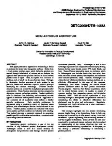
Figure 1: High-level architecture of the multi-lane VP prototyped on a Xilinx FPGA. The vector memory is low-order interleaved. Each vector lane is attached to a private memory.
3
Microprocessors and Microsystems (Elsevier journal), accepted for publication, 2015 2. Methodology and Realized Architecture 2.1 System Architecture Prototyping on FPGA Figure 1 depicts the basic architecture of the FPGA-prototyped VP introduced in this paper. For the sake of simplicity we show a single scalar core, Xilinx’s soft core MicroBlaze (MB) that fetches instructions from its instruction memory (not shown in the figure) and issues them to appropriate execution units. The MB is in charge of executing all scalar and control instructions while vector instructions are sent to the VP. The shuffle engine, which is distributed along the lanes, is activated only to realize vector data shuffling with multiple vector lanes. Our design introduces two innovative concepts. First, it removes the competition of lanes to access memory banks, which is the case for earlier works, by employing cache-less private memories for the lanes; the private memories form a low-order interleaved space that resides between the lanes and the global memory. Second, the vector length can vary even between instructions in the same thread. In all previously introduced VPs, the vector length was defined for each working context, program or thread. It was usually a fixed number for each thread and was set in advance by the scheduler. In contrast, our model allows us to define the vector length for each individual instruction. As a result, the vector length can vary widely, even for instructions in the same loop. Although usage of a mask register could potentially have the same effect, the performance can degrade. Data needed by applications running on the VP should be preferably stored in the private memories of lanes. Since these private memories connect to the AXI (Advanced eXtensible Interface) shared bus, copying the data from the global memory could be done either by the MB or the DMA engine as both have access to the shared bus. If the instruction and data caches also of the MB are placed on the AXI interconnect, the time needed to copy the data from the global memory to either the vector memory or the MB data cache will basically be the same. The same principles are applied for writing back from the VP private memories or the MB data cache to the global memory. Block data are placed in consecutive locations in the MB data cache while low-order interleaving among lanes is used for the vector memory. To evaluate the proposed VP model, we created an FPGA prototype with four lanes and four onchip memory banks that serve as local memories. Our VP model is modular and can be easily extended to include more lanes. We used the Xilinx Virtex6 xc6vlx240t-FF748 FPGA device. To reduce the complexity of the hardware design in order to track operations progressing through the data path, we included rather simple execution units in the vector lanes. Since each lane directly connects only to its private memory in order to avoid contention when accessing memory banks, a very fast load-store unit was designed in each lane as there is no chance of stalling during memory access instructions. Contention when accessing a memory bank can only happen in the case of data shuffle instructions which, however, are totally handled by each lane’s shuffle engine. Since the distributed shuffle engines employ other ports of the private memory banks than those that connect to lanes, other vector instructions can be executed while realizing data shuffling as long as no data hazard exists between the involved instructions. Figure 2 shows the detailed architecture of our prototype. The hardware design of the vector lanes, vector controller, scheduler, data shuffle controller, data shuffle engines, and combinational crossbar and mux was done by writing VHDL code. Xilinx IPs (Intellectual Properties) were used for the realization of the memory banks, memory controllers, MB, and AXI4 and AXI4 Lite interconnects. The VP was developed using Xilinx ISE version 14.5. The MB was added to the project using the EDK tool while its configuration and connection to the peripherals was done using Xilinx XPS. The current paper focuses on proof of concept, so the prototyped VP consists of 4
Microprocessors and Microsystems (Elsevier journal), accepted for publication, 2015 four lanes and has 1024 32-bit registers in the vector register file. It also contains a 64Kbyte vector memory that can accommodate our largest benchmark. The rest of this section contains VP details.
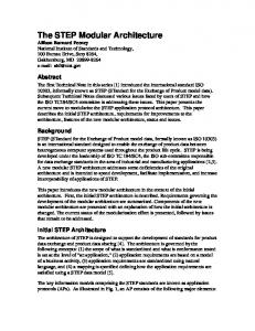
Figure 2: Detailed architecture of the four-lane VP (FP: Floating-point).
The MB soft core is a 32-bit RISC Harvard architecture that supports the AXI4 and LMB (Local Memory Bus bus interfaces. We implemented version 8.40.a with five pipeline stages and a floating-point unit. Data and instruction caches can be connected to either bus. For flexibility, we connect the memory blocks to both the AXI4 and LMB buses. Each bus requires its own memory controller. We use one AXI4 memory controller to create a slave interface for the vector memory. The AXI4 interconnect is good as a shared bus for high-performance memory mapping and can support up to 16 slaves and 16 masters [17]. The AXI4 crossbar can realize every transfer between interconnected IPs, like memories. Moreover, it supports the DMA-based burst mode for up to 256 data transfer cycles which is suitable for transfers between the global and private memories. To connect the VP and shuffle controller to the MB for vector instruction transfers from the MB, the AXI4 Lite interconnect is used which is appropriate for this type of non-DMA memory-mapped transfers. The slave interfaces for connecting the VP and shuffle controllers to the shared bus are developed using the create-and-import peripheral wizard in Xilinx XPS. They both contain control registers which can be read and written by the MB through the AXI4 lite interconnect. A hardwired scheduler for accessing the VP is included in the VP interface. The main responsibility of the scheduler is to grant VP access to a requesting MB based on the vector length it asks for and the current availability of VP vector registers. Vector instructions are written into the VP using memory mapping. 2.2 VP Architecture and Instructions Two types of vector instructions are used by our VP. The first type does not contain data and all the required fields for executing the instruction are placed in the 32-bit instruction; vector-vector ALU instructions are of this type. The other instruction type consumes 64 bits that contain a 32-bit operand value; e.g., vector-scalar ALU instructions are of this type. Since our main focus here is proof of concept for the hardware design, we did not develop an advanced compiler for the VP. Inline function calls are included in the C code for the MB; they represent VP instructions and their realization involves macros. 5
Microprocessors and Microsystems (Elsevier journal), accepted for publication, 2015 Since the VP’s instruction input port is viewed as a memory location by the MB in this memory mapped system, a small delay may occur between issuing an instruction of the second type and the arrival of the needed operand. Thus, the scheduler sends them together to the VP when the data becomes available. Every MB that has access to the AXI4 Lite interconnect can send a request to the scheduler for VP resource access. Each MB can access the VP as a peripheral device using two different addresses, for sending a VP request or release instruction and a vector instruction upon VP granting, respectively. Requests are granted by the scheduler. Threads initiate a request to the scheduler in advance using a 32bit instruction. This request instruction includes the vector length (VL) per register and the number of vector registers needed by the thread. An affirmative reply by the scheduler will include a 2-bit thread ID that can be used to get VP access. This will occur only if there is enough space in the vector register file to accommodate the request. The MB running the thread will include this ID in all vector instructions sent to the VP. Vector register renaming and hazard detection rely on this type of ID. If the aforementioned conditions for the thread are not satisfied, the scheduler will reject the thread request with information about the currently available VL and vector registers. Although our hardware implementation allows different vector instructions to employ different VLs, a complicated register renaming unit will be needed. Therefore, for the sake of simplicity, this paper assumes that the VP can handle two threads at a time, from the same or different MB cores, where all instructions in both threads use the same VL. Otherwise, it will be the compiler’s or programmer’s responsibility to employ registers that will guarantee no conflicts in the VRF (Vector Register File). Threads release VP resources by issuing a release instruction to the scheduler. The VP scheduler interfaces the VP via the VP controller (VC). The latter has a pipelined architecture that consumes three clock cycles for register renaming and hazard detection. Since the VP connects to AXI4 Lite via the shared bus, it can receive instructions from any scalar processor that connects to that bus in a multicore environment; thus, the VC unit can accept vector instructions from a multitude of threads and carry out register renaming, if needed. RAW (Read-After-Write), WAW (WriteAfter-Write) and WAR (Write-After-Read) data hazards are resolved by the hazard detection unit in the VC. This unit resolves all possible hazards in accessing vector registers in the lanes by using an appropriate instruction tagging mechanism. Adding a tag to each instruction allows handshaking between the VC and VP. The same instructions are issued simultaneously to all four lanes. The detailed architecture of each lane is depicted in Figure 3. The data paths for memory and ALU instructions are completely separated in each lane, and related instructions and data are queued in different FIFOs. All the instructions and data in a lane are represented using 32 bits. Memory accessing instructions always contain 32-bit additional data to represent the private memory base address to be used. ALU instructions for vector-scalar operations also contain a 32-bit floating point scalar. ALU instructions are decoded by the ALU decode unit and the needed operands are fetched from the VRF. The VRF in each lane consists of 256 32-bit locations that can store 256 single-precision floating-point vector elements. It is accessed using three read and two write ports since the ALU and load (part of the loadstore LDST) units need two and one read port in order to simultaneously read two and one operand, respectively, and the register WB (Write-Back) and store (part of LDST) units require one write port each. In the case of contention, when different ports want to perform different tasks simultaneously on the same location in the VRF, the write first policy could be applied. The design results in one clock cycle latency for sending the output to related ports; it uses output enable ports to ease the reading task. Reading from the VRF is possible only when the output enables are triggered. The ALU decode unit requires two read ports when reading a pair of floating-point operands to realize vector-vector 6
Microprocessors and Microsystems (Elsevier journal), accepted for publication, 2015 instructions. The ALU execution unit in the lane contains a floating-point adder/subtractor and a multiplier that were developed using open source code [18]. This unit has six pipeline stages for addition and subtraction, and four stages for multiplication; it performs operations on 32-bit single-precision floating-point data. The results of the execution unit are sent to the WB block which connects to a write port of the VRF for writing one element per clock cycle in a pipelined fashion.
Figure 3: Lane architecture.
Absolute and indexed memory addressing are used to access the private memories. Absolute addressing may employ a non-unit stride. The LDST unit fetches the register content for a store instruction from the VRF and generates the destination address for the lane’s private memory using the base address that arrived right after the instruction. It uses only one VRF read port. Each vector memory instruction issued to the lane has two 32-bit fields. The first field contains the source or destination register and the stride value, whereas the second one is a base address in the lane’s private memory. Indexed addressing for the private memory is realized using the data shuffle engines. For load instructions, the WB unit writes the fetched memory contents into the proper register using a write port at the rate of one element per clock cycle. In our prototyped VP with four lanes, 1024 (i.e., 4 lanes *256 elements/lane) vector elements can reside in the VRF; the VRF is divided evenly among the four lanes so the VL must be a multiple of four. Hence, we can configure the VRF as 16 vector registers with VL=64, or 32 registers with VL=32, or 64 registers with VL=16. The location of register elements in the VRF depends on the VL value and the register ID. In the case of VL=64, for example, register “r0” contains all the elements of “r0” and “r1” for VL=32. The ALU and LDST decode blocks in each lane include counters for synchronization when reading from the VRF and feeding the data to the next block; they are initialized based on the VL assumed by the instruction. Since our design avoids memory stalls by making a private memory available to each lane, all lanes remain synchronized in the full pipeline utilization mode where one element is processed every clock cycle in the lane. This synchronization flexibility allows dynamic changes of VL’s value for any given instruction. For example, the vector-vector instruction “r2