Molekul, Vol. 11. No. 2, November 2016: 202 – 207
doi: 10.20884/1.jm.2016.11.2.230
PREPARATION OF COPPER OXIDE NANOSTRUCTURE THIN FILM FOR CARBON MONOXIDE GAS SENSOR PEMBUATAN LAPISAN TIPIS TEMBAGA OKSIDA BERSTRUKTUR NANO UNTUK SENSOR GAS KARBON MONOKSIDA Brian Yuliarto1,2, Suyatman1*, Ni Luh Wulan Septiani1,2, Nugraha1,2, Gentry Rafa1 1
Advanced Functional Materials Laboratory, Engineering Physics Department, Institut Teknologi Bandung, Bandung, Indonesia 2 Research Center for Nanosciences and Nanotechnology, Institut Teknologi Bandung, Bandung, Indonesia email:
[email protected] Received 18 August 2016; Accepted 28 October 2016; Available online 29 November 2016 ABSTRACT This work reports the synthesis of the nanostructure of CuO thin film using dip coating and chemical bath deposition method. Seed layer was deposited by dip coating method using zinc nitrate as a precursor. The CuO nanostructure has been successfully grown using CBD process at 95 °C for 6 hours. The X-Ray Diffraction characterization result shows that the CuO has monoclinic crystallization and good crystallinity. Moreover, the Scanning Electron Microscope characterization results show that CuO has nanospike-like shape. The CuO thin film as a gas sensor shows a relatively high response on CO gas at the temperature working above 200 °C. The highest response is obtained at 350 °C of working temperature toward 30 ppm CO gas at 186% of sensor response. Keywords: Copper oxide, nanostructure thin films, carbon monoxide, gas sensor. ABSTRAK Artikel ini melaporkan pembuatan atau sintesis lapisan tipis CuO berstruktur nano menggunaan metode dip coating dan chemical bath deposition. Lapisan seed di deposisikan dengan metode dip coating menggunakan zinc nitrat sebagai precursor. CuO berstruktur nano telah berhasil ditumbuhkan dengan proses CBD pada temperatur 95 °C selama 6 jam. Karakterisasi dengan menggunakan X-Ray Diffraction menunjukan bahwa CuO memiliki struktur kristal monoklinik dan memiliki kristalinitas yang baik. Selain itu, karakterisasi dengan menggunakan Scanning Electron Microscope menunjukan bahwa CuO memiliki bentuk morfologi nanospike-like. Lapisan tipis CuO sebagai sensor gas menghasilkan respon yang relatif tinggi pada suhu di atas 200 °C. Respon tertinggi terhadap 30 ppm gas CO diperoleh CuO pada temperatur kerja 350 °C yaitu 186%. Kata kunci : Tembaga oksida, lapisan tipis berstruktur nano, karbon monoksida, sensor gas.
INTRODUCTION In recent times, the fast growing of vehicles has affected greatly on air quality especially in big cities Indonesia. Based on Statistic Center Agency, the growing of the vehicles reaches 10.39% every year (Badan Pusat Statistik, 2014). The vehicles emit the harmful gasses including carbon monoxide (CO) which is very dangerous for both human and environment (Arabloo et al., 2015; Gosh.,
2014; Yuliarto.,2015). This gas is colorless and odorless so that it is very difficult to be detected by a human. CO can bind hemoglobin in red blood and prevent red blood cells to bind oxygen (Gosh, Narjinary, Sen, Bandyopadhyay, & Roy, 2014). This gas can cause death if inhaled in high concentration (Arabloo et al., 2015; Gosh., 2014; Yuliarto.,2015). The characteristic and the dangerous of CO gas yield the demand of gas sensor to
202
Preparation of Copper Oxide Nanostructure Thin Film detect the existence and monitor the concentration of CO gas. Gas sensor based on metal oxide becomes the favorite because it has high sensitivity and relatively low cost (Yuliarto, 2015; Septiani, 2016). In recent years, decreasing the size of metal oxide become the main focus because particles with nanoscale size significantly improve the properties of metal oxide compare with the bulk form (Javed, Usman, Tabassum, & Zia, 2016). In the case of the gas sensor, decreasing size of metal oxide can significantly improve the sensitivity. Copper oxide (CuO) is one of p-type semiconductor that has band gap range 1.21-1.51 eV and has potential as a gas sensor (Muiva, 2016; Ayesh, 2016; Liu, 2016). CuO has high catalytic activity, unique electrochemical characteristic and high oxygen adsorption (Asad & Sheikhi, 2016). There are many methods that have been developed for the synthesis of this material such as hydrothermal and solvothermal. In this work, we used Chemical Bath Deposition (CBD) to fabricate CuO nanostructure thin film. CBD is one of wet route method that has several advantages including simple set up, low-cost equipment, large scale production, easy to adjustment the parameter and relatively low-temperature synthesis (Manthina, 2016; Shi, 2016; Bahramian, 2016). The resulting CuO nanostructure thin films deposited by CBD were then testing toward CO gas at various working temperature and concentrations. EXPERIMENTAL SECTION The materials that used in this work are Zn(CH3COO)2.6H2O, Cu(NO3)2. 3H2O, Hexamethyl Tetraamine (HMTA), and deionized water. All the materials are pro analysis and used without any further purification. The first step in this work is seed layer deposition on the substrate by dip coating method. The solution for dip process was prepared by mix Zn(CH3COO)2.6H2O, HMTA, and deionized water. A certain amount of 203
Brian Yuliarto et al.
Zn(CH3COO)2.6H2O and HMTA were mixed by a magnetic stirrer in 60 mL deionized water at 60 °C for 1 hour. After several time of washed using water, the alumina substrate was dipped in the solution for 10 seconds and was dried in the microwave at 100 oC for 30 minutes. The next step is deposition of CuO nanostructure thin films by CBD process. Several amounts of Cu(NO3)2. 3H2O dan HMTA were mixed with a stirrer for 60 minutes at room temperature. The substrate having seed layer was then immersed in the solution for 6 hours at 95 °C. After that, the samples were then calcined at 450 °C for 2 hours. The crystallinity, morphology and composition of CuO nanostructure thin films were investigated by X-Ray Diffraction (XRD), Scanning Electron Microscope (SEM), and Energy Disperse, respectively. The CO gas sensor testing was conducted at 200-350 °C toward 30 ppm CO. The testing was repeated for five times each sample. The sensitivity of the sensor was tested by varied the concentration of gas at 10, 50, and 100 ppm. The sensor was also tested with NO gas to get their selectivity of the sensor. Variation concentration of CO and NO were confirmed by Bacharach gas detector PCA3 type. RESULTS AND DISCUSSION Figure 1 shows X-Ray diffraction pattern of CuO nanostructure thin films on an alumina substrate. From the pattern, there are two phases that were come from CuO of nanostructure thin film and Al2O3 of the alumina substrate. The alumina was still detected because the film is very thin which is about hundreds of nanometers so that the X-Ray could detect the alumina structure. The strong peaks of CuO in 2θ = 35.662° dan 38.853° yielded by (-111) structure, indicate that the CuO has good crystallinity and has a monoclinic crystal structure, which is matched with JCPDS (Joint Committee of Powder Diffraction Standard) card no 41-0254.
Molekul, Vol. 11. No. 2, November 2016: 202 – 207
doi: 10.20884/1.jm.2016.11.2.230
Figure 1. X-Ray Diffraction pattern of CuO nanostructure thin films
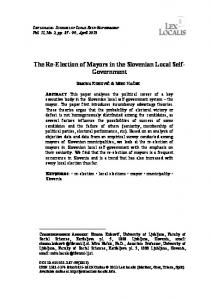
(a)
(b)
Figure 2. The SEM image of CuO nanostructure thin films with different magnitude with scale bar equals to (a) 5 µm and (b) 1 µm Figure 2 shows the morphology of CuO nanostructure thin film from the SEM image. It can be seen from Figure 2 that the CuO thin film has nano spike pattern. In the SEM image with scale bar at 5 µm, the CuO nanostructure thin films shows that incomplete agglomeration is occurred and the nano spike is not visible, but in the SEM image with scale bar 1 µm the nano spike is clearly visible. The Figure 2 also shows that the CuO
nanostructure thin film has many pores that can help the targeted gas to diffuse deeply into the sensitive layer of CuO nanostructure thin films and increase the response of sensor toward CO gas. Figure 3 shows EDS characterization result of CuO nanostructure thin films. It shows that there is only one phase in the thin film sample from CuO nanostructure thin film structure indicating that there is no impurity in the sample.
Figure 3. Energy Dispersive Spectroscopy spectrum of CuO nanostructure thin film
204
Preparation of Copper Oxide Nanostructure Thin Film
Brian Yuliarto et al.
Figure 4. The typical dynamic response of CuO nanostructure thin film toward 30 ppm at 200°C-350 °C of working temperature The CuO nanostructure thin film is found out sensitive to the exposure of CO gas in the range of working temperature between 200 °C and 350 °C. In this case, the CuO nanostructure thin film has high resistance and start to show a response at 200 °C. The CuO thin film sensor was tested until 350 °C because the sensor with high operation temperature is not expected because of high-energy consumption as shown in Figure 4. At 200 °C the CuO nanostructure thin film shows very little response indicating that at the working temperature of 200 °C the reaction between targeted gas and the surface sensitive layer occurred rarely. Figure 4 shows that the sensor response toward 30 ppm increases as the increasing of working temperature. This phenomenon occurred because at a higher temperature, the CO gas has more energy to absorb and interact with oxygen ion in the surface of CuO nanostructure thin
film. CuO is p-type semiconductor where the majority carrier is a hole (Umar, 2016). CO gas is a reduction gas and the interaction between the CO gas, and ptype semiconductor can cause the increasing of resistance of the material. The resistance of CuO nanostructure thin film increases when the CO gas has interaction with O- ion of oxygen on the surface of CuO and this interaction release electrons. The electrons will recombine with the hole and decrease the charge carrier, which led to the increasing resistance of CuO surface. At 200 °C, the resistance of CuO is still too high so that the changing of resistance caused by the surface reaction is very small. The surface reaction can be as follow (Yuliarto, 2015; Kocemba, 2011), (1) (2)
Figure 5. The sensitivity of CuO toward different concentration of CO. 205
Molekul, Vol. 11. No. 2, November 2016: 202 – 207 Moreover, to investigate the linearity, the CuO nanostructure thin film sensors is exposed the CO gas toward various concentration on 10, 30, 50, and 100 ppm at 350 °C of working temperature. The sensor response increases as the increasing of CO gas concentration as shown in Figure 5 indicates that the CuO nanostructure thin film sensor has good linearity. The sensor also still reveals good response at the 10 ppm concentration of CO gas. The increasing amount of CO gas would increase the interaction between the CO gas and the surface of CuO nanostructure thin film sensor. CONCLUSION The CuO nanostructure thin film has been successfully fabricated on alumina substrate using dip coating and chemical bath deposition method. The resulting CuO nanostructure thin film has good crystallinity with nanospike pattern on the surface. The CuO nanostructure thin film shows a good response in the range of 200 °C to 350 °C toward the 30 ppm of CO gas. The CuO nanostructure thin film sensors can detect as low as 10 ppm of CO gas at the working temperature of 350°C. REFERENCES Arabloo, F., Javadpour, S., Memarzadeh, R., Panahi, F., Emami, M.D., Shariat, M.H. (2015).The interaction of carbon monoxide to Fe (III)(salen)-PEDOT:PSS composite as a gas sensor. Synthetic Metals, 209, 192-199. Asad, M., Sheikhi, M.H. (2016). High sensitive wireless H2S gas sensors at room temperature based on CuOSWCNT hybrid nanomaterials. Sensors and Actuators B: Chemical, 231, 474-483. Ayesh, A.I., Abu-Hani, A.F.S., Mahmoud, S.T., Haik, Y. (2016). Selective H2S sensor based on CuO nanoparticles embedded in organic membranes.
doi: 10.20884/1.jm.2016.11.2.230
Sensors and Actuators B: Chemical, 231, 593-600. Bahramian, R., Eshghi, H., Moshaii. (2016). Influence of annealing temperature on morphological, optical and UV detection properties of ZnO nanowires grown by chemical bath deposition. Materials & Design, 107, 269-276. Gosh, S., Narjinary, M., Sen, A., Bandyopadhyay, R., Roy, S. (2014). Fas detection of low concentration carbon monoxide using calciumloaded tin oxide sensors. Sensors and Actuators B : Chemical, 203, 490-496. Javed, R., Usman, M., Tabassum, S., Zia, Muhammad. (2016). Effect of capping agent: Structural, optical and biological properties of ZnO nanoparticles. Applied Surface Science, 386, 319-326. Kocemba, I., Rynkowski. (2011). The influence of catalytic on the response of Pt/SnO2 gas sensors to carbon monoxide and hydrogen. Sensors and Actuators B, 155, 659666. Liu, X., Hu, M., Wang, Y., Liu, J., Qin, Y. (2016). High sensitivity NO2 sensor based on (CuO/p-porous silicon heterojunction at room temperature. Journal of Alloys and Compounds, 685, 364-369. Manthina, V., Agrios, A.G. (2016). Single-pot ZnO nanostructure synthesis by chemical bath deposition and their application. Nano-Structures & Nano-Objects, 7, 1-11. Muiva, C.M., Maabong, K., Moditswe., C. (2016). CuO nanostructured thin films synthesized by chemical bath deposition on seed layers deposited by successive ionic layer adsorption and reaction and chemical spray pyrolysis technique. Thin Solid Films, 616, 48-54. Septiani, N.L.W., Yuliarto, B. (2016). The development of gas sensor based on
206
Preparation of Copper Oxide Nanostructure Thin Film carbon nanotubes. Journal of The Electrochemical Society, 163, B97B106. Shi, Z., Walker, A.V. (2016). Zinc oxide chemical bath deposition on functionalized organic thin films: Formation of nanorods, nanorockets and nanoflower. Thin Solid Films, 606, 106-112. Suryamin. (2014). Statistik Transportasi Darat. Jakarta : Badan Pusat Statistik. Umar, A., Lee, J.-H., Kumar, R., AlDossary, O., Ibrahim, A.A., Baskoutas, S. (2016). Development of highly sensitive and selective ethanol sensor based on lanceshaped CuO nanostructures. Materials & Design,105, 16-24.
207
Brian Yuliarto et al.
Yuliarto, B., Gumilar, G., Septiani, N.L.W. (2015). SnO2 nanostructure as pollutant gas sensors : Synthesis, sensing performances, and mechanism. Advances in Materials Science and Engineering, 2015, 114. Yuliarto, B., Nulhakim, L., Ramadhani, M.F., Iqbal, M., Nugraha, Suyatman, Nuruddin, A. (2015). Improve performances of ethanol sensor fabricated on Al-doped ZnO nanosheet thin films. IEEE Sensors Journal, 15, 4114-4120.