16. - 18. 10. 2013, Brno, Czech Republic, EU
MONTE CARLO SIMULATION OF PROXIMITY EFFECT IN E-BEAM LITHOGRAPHY Michal URBÁNEK, Vladimír KOLAŘÍK, Stanislav KRÁTKÝ, Milan MATĚJKA, Miroslav HORÁČEK, Jana CHLUMSKÁ ISI ASCR, v.v.i., Královopolská 147, 612 64 Brno, Czech Republic,
[email protected]
Abstract: E-beam lithography is the most used pattern generation technique for academic and research prototyping. During this patterning by e-beam into resist layer, several effects occur which change the resolution of intended patterns [1]. Proximity effect is the dominant one which causes that patterning areas adjacent to the beam incidence point are exposed due to electron scattering effects in solid state [2]. This contribution deals with Monte Carlo simulation of proximity effect for various accelerating beam voltage (15 kV, 50 kV, 100 kV), typically used in e-beam writers. Proximity effect simulation were carried out in free software Casino and commercial software MCS Control Center, where each of electron trajectory can be simulated (modeled). The radial density of absorbed energy is calculated for PMMA resist with various settings of resist thickness and substrate material. At the end, coefficients of proximity effect function were calculated for beam energy of 15 keV, 50 keV and 100 keV which is desirable for proximity effect correction. Keywords: Monte-Carlo, proximity effect simulation, e-beam lithography. 1.
INTRODUCTION
Nowadays, e-beam writing technology is a method for creating very fine patterns in academic and research prototyping. This method is based on the interaction of focused electron beam with resist layer (polymer material) deposited in most cases on silicon wafer. During the writing, the scatering effects affecting the final pattern occur. First is forward scattering due to this the initial beam diameter is broaden. The broadening of the beam is given empiracally and it can be minimized by using the highest possible accelerating voltage. Second one is backsacttering where the electrons undergo large angle scattering angle events.The result of scattering effects is that areas nearby from beam incidence point are exposed or isolated patterns lose much of dose. The combination of this scattering effects is called proximity effect and can be described by two Gaussian distribution of absorbed energy in resist layer. This contribution deals with another aproach which is Monte Carlo simulation of each individual electron trajectory penetrating the resist layer and substrate [3]. The density of absorbed energy in resist can be modeled for various acellerating voltages, various resist material and thicknesses. Parameter of backscattered electrons is calculated from simulated trajectories which can be implemented in Gaussian model to prevent proximity effect which is desirable for pattern generation in high resolution [4]. 2. 2.1
MONTE CARLO SIMULATION CASINO software
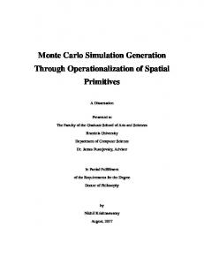
This software enables simulations of individual electron trajectories for various settings of thicknesses, materials and beam voltages. The trajectories of 200 primary electrons projected onto x-z plane for beam voltage of 15 and 100 kV and PMMA thickness of 500 nm are shown in Fig.1 and Fig. 2.
16. - 18. 10. 2013, Brno, Czech Republic, EU
Fig. 1: Simulated trajectories of 200 electrons in PMMA layer (500 nm) on silicon for beam voltage 15 kV.
Fig. 2: Simulated trajectories of 200 electrons in PMMA layer (500 nm) on silicon for beam voltage 100 kV. As obvious, the penetration depth of electrons into substrate material is higher for higher beam voltage, accordingly this the using of higher beam voltage is one possibility of proximity effect compensation.
16. - 18. 10. 2013, Brno, Czech Republic, EU
CASINO software allows to calculate radial density of absorbed energy in PMMA and substrate (Fig.3) but due to complicated data export into graph, software MCS Control Center, described in next section, was used.
Fig.3: Equienergy density contours for beam voltage of 15 kV and PMMA thickness of 500 nm. 2.2
MCS Control Center software
Comercial software MCS Control Center is more complex and it allows to calculate radial density of absorbed energy and proximity effect parameters for various materials, the thicknesses of material and beam voltages. The values of proximity effect parameters are listed in Table 1, these parameters can be exploited in proximity effect corection [5]. The parameter is bigger for higher beam voltage it means that using higher beam voltage is preferable for pattern generation with high resolution. The parameter remains constant for all beam voltages and PMMA thicknesses. Figure 4 shows the radial distribution of absorbed energy calculated with 1 000 000 electrons for beam voltages of 15 and 100 kV and PMMA thicknesses of 500 nm. Table 1: Proximity effect parameters
beam voltage [kV]
15 kV
50 kV
100 kV
= 0,002 m
= 0,002 m
= 0,002 m
1,069 m
9,147 m
32,665 m
= 0,002 m
= 0,002 m
= 0,002 m
1,376 m
9,369 m
32,765 m
PMMA thickness [nm]
50
500
16. - 18. 10. 2013, Brno, Czech Republic, EU
Fig. 4: Radial distribution of absorbed energy in material 15 kV – top, 100 kV – bottom. 3.
CONCLUSION
Monte Carlo simulation in two different softwares were carried out. The radial density of absorbed energy in PMMA and substrate was calculated for various beam voltages and PMMA thicknesses. Proximity effect parameters for double Gaussian function were determined. ACKNOWLEDGMENT This work was partially supported by the EC and MEYS CR (project No. CZ.1.05/2.1.00/01.0017 ALISI, project No. CZ.1.07/2.3.00/20.0103 OPVK), the TACR project No. TE 01020233 and by the institutional support RVO: 68081731. REFERENCES [1]
RAI-CHOUDHURY, P. Handbook of Microlithography, Micromachining and Microfabrication. Volume 1: Microlithography. 1. edit. SPIE Press Monograph: Washington, 1997, ISBN 0-8194-2378-5.
[2]
URBANEK, M. et al., Determination of proximity effect forward scattering range parameter in E-beam lithography. In proceedings of12th Recent Trends in Charged Particle Optics and Surface Physics Instrumentation, Skalský Dvůr, Czech Republic , 2010, p. 67-68, ISBN 978-80-254-6842-5.
[3]
KYSER, D.F., VISWANATHAN, N.S., Monte Carlo simulation of spatially distibuted beams in electron –beam lithography, Journal of Vacuum Science and Technology , 12, 1975, p.1305-1308.
[4]
KOLARIK, V. et al., Proximity effect simulation for variable shape E-beam writer. In proceedings of13th Recent Trends in Charged Particle Optics and Surface Physics Instrumentation, Skalský Dvůr, Czech Republic , 2012, p. 75-76, ISBN 978-80-87441-07-7.
[5]
URBANEK, M. et al., Shaped E-beam nanopatterning with proximity effect correction, In proceedings of Nanocon 2012, 1. edit. TANGER Ltd: Ostrava, 2012, p. 61, ISBN 978-80-87294-32-1.