MOSIS CMOS Scalable Rules An Example of Scalable Design ...
Recommend Documents
May 11, 2009 ... Vendor-independent, scalable rules (MOSIS SCMOS Rules) ... MOSIS Scalable
CMOS (SCMOS) is a set of logical layers together with their ...
Oct 4, 2004 ... MOSIS Scalable design rules require that layout is on a 1/2 lambda grid. ...
MOSIS has defined an optional layer (called XP in CIF and ...
principle hash, range or k-d based with respect to the partitioning key(s). The storage .... Each constraint defines the partition (primary) key range of the segment.
The SERDES circuits contribute greatly to power consumption at these frequencies. More recently in [9], the impact of the low latency and absence of contention ...
Kyle Preston, Nicolás Sherwood-Droz, Jacob S. Levy, and Michal Lipson. School of Electrical and Computer Engineering, Cornell University, 428 Phillips Hall, ... As high-performance computing systems and data centers continue to achieve ...
course on CMOS Analog I.C. Design offered at our department, design of a
CMOS .... Two textbooks are used: Allen and Holberg's[1] serves as an excellent
...
Dec 13, 2005 - Server UPDATE command clauses allowed for a distributed ..... Dell o R iew of PhotoObj scalable table. The merge of under-loaded segments ...
Pride and Prejudice also buy Emma within a month". Such patterns are ...... cessors/host) inter-connected by the Memory Channel Gillett, 1996] network. The.
group at IBM Almaden Research Center. Thanks to Dr. Mitsunori ...... ACD. DTW. CTW. AC. ACTW. CDW. Maximal Frequent Itemsets: ACTW, CDW. Figure 2.3: The .... We therefore call k a pre x-based equivalence relation. Figure 2.6 shows ...
synthesizing analog piecewise-linear (PWL) computing circuits using the MP principle. MP circuits use only addition, subtraction and threshold operations and ...
Jun 5, 2014 - candidate to realize large scale quantum information processing, as it ..... Lithographic mask of a quantum register made of 8 logic qubits (A-H).
assigned size of send socket buffer is too large for client A and it is too insufficient for client B. This is because the network capacity (more strictly, ...
system. The paper presents design patterns of scalable cluster system software, including scalable software topologies and optimized communication modes.
Jul 15, 2013 - Ranajit Sai , K.J. Vinoy , Navakanta Bhat , and S. A. Shivashankar. Centre for Nano Science and Engineering, Indian Institute of Science, ...
current-mode analog computational circuits is based on the translinear principle which exploits the exponential current-to- voltage relationship observed in ...
Design of a Self-evolving Scalable Matching. Network for OCEAN. Pradeep Padala and Michael P. Frank. Computer & Information Science & Engineering.
The design pattern of cluster system software has an ... According to recent TOP500 lists of supercomputer ... scheduling and job management capabilities, d).
comparing two (or more) configurations for large work- loads. Solving this ... First, the accuracy of the estimation depends crit- ically on the .... ble or file, and evaluating its cost using the query optimizer. ... and Cj, which we write as Pr(CSl
If the server host assigns an equal size of the send socket buffer to both clients, it is likely that an amount of the assigned buffer is too large for client A, and too ...
Exact and Heuristic data Workflow Placement Algorithms for Big Data. Computing in Cloud Datacenters. 223. Sonia Ikken, Eric Renault, Abdelkamel Tari, M. Tahar Kechadi. Significance ...... [3] Sammer, E.: Hadoop operations. O'Reilly Media ...
The development of IoT has led to an increase of data generated. ⢠Since anonymization is mandatory, those data needs to be processed by Mondrian as quickly ...
mentations of synapse plasticity, which limits portability to advanced technology nodes. On-chip synaptic learning was demonstrated with binary synapses in [7], ...
from Cascade Microtech, with a ceramic impedance standard substrate. Subsequent to the probe tip calibration, the pads used to test the passives fabricated on ...
MOSIS CMOS Scalable Rules An Example of Scalable Design ...
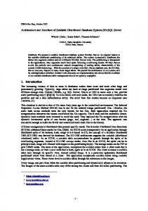
An Example of Scalable Design Rules for Integrated Circuit Layout The following pages contain an example of a typical set of design rules that is used by the MOSIS integrated circuit fabrication service. The symbol names, colors, and patterns for the different layers refer to the MAGIC layout software package.
MOSIS CMOS Scalable Rules LAYER
SYMBOL MIN. DIM. COLOR PATTERN
NDIFFUSION
ndiff
3
green
PDIFFUSION
pdiff
3
brown
POLYSILICON
poly
2
red
METAL1
m1
3
blue
METAL2
m2
3
purple
NWELL
nwell
10
lt. green
PWELL
pwell
10
lt. brown
CONTACT
m2c, pc, ndc, pdc, nnc, ppc
2 M1
1
M2
COMMENTS 1. ALL CONTACTS ARE WITH RESPECT TO THE METAL1 LAYER (e.g. pc= m1 to poly). 2. DIMENSIONS ARE IN UNITS OF LAMBDA FOR GENERAL LAYOUTS OR MICRONS FOR 2.0 MICRON TECHNOLOGY (LAMBDA = 1.0). 3. A SUBSTRATE OR WELL CONTACT MAY BE SHOWN BY A FREE STANDING CONTACT OR BY A DOUBLE CONTACT AT THE SOURCE OF A TRANSISTOR. 4. DIMENSIONS GIVEN ARE MINIMUM VALUES, EXCEPT FOR CONTACT SIZES WHICH MUST BE EXACTLY 2 X 2 AS SHOWN.
RULES A. ACTIVE (TRANSISTOR) POLY GATE OVERLAP
POLY WIDTH ACTIVE TO CONTACT 2
NDIFF WIDTH 2
2
3
2
CONTACT
1 FIELD POLY TO DIFFUSION
3
3 DIFFUSION BEYOND POLY GATE
SUMMARY OF RULES: 1. MINIMUM DIFFUSION WIDTH = 3 2. MINIMUM POLY WIDTH = 2 3. MINIMUM SPACING OF FIELD POLY TO DIFFUSION = 1 4. POLY GATE OVERLAP OF DIFFUSION = 2 5. EXTENSION OF DIFFUSION BEYOND POLY GATE = 3 6. MINIMUM POLY GATE TO CONTACT = 2 7. CONTACT IS EXACTLY 2 X 2 2
B. GENERAL WIDTHS AND SPACINGS 2
2
3
3
3
3
3
3
2
3
3
4
POLY
DIFFUSION
METAL1
METAL2
10
10
10
4
9
PWELL
NWELL
DIFFUSION TO WELL EDGE
DIFFUSION CONTACT
CONTACT AND OVERLAP 4
5
5
5
1
5 DIFFUSION TO WELL
3
CONTACT OVERLAP WELL/SUBSTRATE CONTACT 3 WELL CONTACT DIFFUSION TO WELL EDGE ACTIVE TO SUBS/WELL CONTACT
5. MINIMUM WELL WIDTH = 10 MINIMUM WELL SPACING = 4 MIN PWELL TO NWELL SPACING = 9
12. MIN OVERLAP PLUS CONTACT = 4 3
C. OTHER CONTACTS 2
2
2
2
1
POLY
DIFFUSION
4
DIFFUSION
5
4 2 many contacts
6
DIFFUSION
2 2
3
2
2 VIA (M2 TO M1)
ALTERNATE VIA (M2 TO M1)
VIA (M2 TO M1)
SUMMARY OF RULES: 1. MULTIPLE POLY/DIFFUSION CONTACT SPACING = 2 2. POLY/DIFF/METAL OVERLAP OF CONTACT = 1 3. CONTACT TO TRANSISTOR CHANNEL = 2 4. DIFF CONTACT TO POLY CONTACT = 4 5. FIELD POLY TO DIFF W/ MULTIPLE CONTACTS = 2 6. POLY CONTACT TO POLY CONTACT = 5 7. POLY CONTACT TO FIELD POLY = 4 8. METAL2 ONLY CONNECTS TO METAL 1 9. A VIA MUST BE ON A FLAT SURFACE BY SPACING CONTACTS 3 UNITS WHEN NO DIFF/POLY IS UNDERNEATH OR EXTENDING DIFF/POLY 2 UNITS BEYOND THE VIA ON ALL SIDES. UNRELATED DIFF/POLY TO VIA = 2. 10. CONNECT METAL2 TO DIFF/POLY BY FORMING A METAL2 TO METAL1 VIA AND THEN A METAL1 TO DIFF OR POLY CONTACT. 4