Multi-Dimensional Modulation Technique for Cascaded Multilevel Converters J. I. Leon, Member, IEEE, S. Kouro, Member, IEEE, S. Vazquez, Member, IEEE, R. Portillo, Member, IEEE, L. G. Franquelo, Fellow Member, IEEE, J. M. Carrasco, Member, IEEE and J. Rodriguez, Member, IEEE
Abstract—Multilevel cascaded H-bridge converters have found industrial application in the medium voltage high power range. In this paper, a generalized modulation technique for this type of converters based on a multi-dimensional control region is presented. Using the multi-dimensional control region, it is shown that all previous modulation techniques are particularized versions of the proposed method. Several possible solutions to develop a specific implementation of the modulation method are addressed in order to show the potential possibilities and the flexibility of the proposed technique. In addition, a feedforward version of this technique is also introduced to determine the switching sequence and the switching times avoiding low harmonic distortion with unbalanced dc voltages. Experimental results are shown in order to validate the proposed concepts. Index Terms—Cascaded multilevel converters, modulation algorithm.
I. I NTRODUCTION
M
ULTILEVEL converters are especially designed to be used in applications where a high power demand and a high quality of the output waveforms are required [1]– [4]. Several topologies have found industrial acceptance: the already classical 3-level neutral point clamped (3L-NPC), Cascaded H-Bridge (CHB) and four level Flying Capacitor (4L-FC) [4]; and the more recent active NPC (ANPC) [5], the modular multilevel converter (MMC) [6], [7] and the five level H-bridge NPC (5L-NPC) [8], [9]. This paper focuses on the CHB, which is commercially available by several manufacturers and covers a power range of 0.15 to 120MW, output voltages up to 13.8kV, output frequency up to 330Hz, and is available in 7, 9, 11, 13 and 17-level configurations (3, 4, 5, 6, and 9 cells per phase respectively), with 18, 30 and 36 multipulse diode rectifiers and even with a regenerative option (2-level 3-phase VSI front end per cell) [10]–[14]. The industrial CHB is composed of low voltage IGBTs, is modulated with phase shifted PWM, and features air-cooling system. Currently their main application Manuscript received June 30, 2009. Accepted for publication April 12, c 2009 IEEE. Personal use of this material is permitted. 2010. Copyright ° However, permission to use this material for any other purposes must be obtained from the IEEE by sending a request to
[email protected]. J. I. Leon, S. Vazquez, R. Portillo, L. G. Franquelo and J. M. Carrasco are with the Electronic Engineering Department, University of Seville (Spain), (e-mail:
[email protected]). S. Kouro is with the Department of Electrical and Computer Engineering, Ryerson University, Toronto, ON M5B 2K3, Canada (e-mail:
[email protected]). J. Rodriguez is with the Electronics Engineering Department, Universidad Tecnica Federico Santa Maria, 2390123 Valparaiso, Chile (e-mail:
[email protected]).
fields are pump, fans, compressors, extruders, kneaders, mixers, crushers, agitators, and conveyors in the medium voltage range [15]. In addition, it has been recently proposed for other applications like: photovoltaic power conversion system [16], [17], wind power conversion [18], and traction with medium frequency isolation transformer [19], [20]. In particular the CHB has great potential for reactive power compensation and active filter applications, since no multipulse transformerrectifier circuit is necessary (which is his main drawback compared to other multilevel topologies) [21], [22]. The modulation of multilevel converters is a important research focus during the last years. In order to determine the switching of the CHB, several modulation strategies have been developed. Multi-carrier based pulse width modulation (PWM) (such as level-shifted PWM and phase-shifted PWM), spacevector modulation (SVM), hybrid modulation or time-based modulation techniques have been applied to CHB achieving a high performance [23]–[30]. Each modulation technique is focused on the optimization of some converter feature such as switching losses reduction, maximum effective switching frequency, even power distribution among the power cells, common-mode voltage minimization, minimum computational cost, etcetera. A good and brief classification of the most common modulation techniques for CHB is presented in [15], [31]. The CHB converter presents great possibilities due to its cascaded connection. Any optimization criterion can be studied developing the corresponding specific modulation technique. The aim of this paper is to introduce a new generalized modulation technique showing the potential of the CHB topology. In this paper, it will be demonstrated that all previous modulation techniques (multi-carrier PWM, SVM, hybrid modulation, etcetera) are only particular solutions of the proposed modulation technique. So, any other modulation strategy could be developed in order to optimize some converter feature. Considering the concepts introduced in this paper, new alternatives in the modulation strategies are opened. The proposed modulation strategy will be focused on the 2CCHB topology but it will be extended for CHB with more than two H-bridges in section V. As a second contribution of the paper, a feed-forward version of the proposed modulation strategy is introduced in order to avoid possible low harmonic distortion due to voltage unbalance in the dc sources of the converter. This paper is an updated and extended version of a previously published paper in IEEE ICIT 2009 Conference [32] and
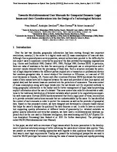
Diode bridge
S11 C1
VC1
Utility Grid
Diode bridge Transformer with configurable secondaries
V1
VC2
S12
S11
S12
S21
S22
C2
V2
S21
a
Vab
Load
S22 b
Fig. 1. Two-cell cascaded H-bridge inverter (2C-CHB) connected to the grid through a transformer with configurable secondaries and diode bridges. This figure also shows the diagram of the test-bench used to obtain the experimental results.
is organized as follows: The proposed generalized modulation method for CHB is presented in section II. The feed-forward version of this modulation technique is presented in section III. The experimental results of the proposed method are introduced in section IV. The extension of the method to be applied to CHB with more than two cells is introduced in section V. Finally, the conclusions of the work are summarized in section VI.
TABLE I G ATE DRIVER SIGNALS DEPENDING ON THE H- BRIDGE i STATE H-bridge i voltage Vi −VCi 0 0 VCi
H-bridge i state Hi 0 1 1 2
Gate driver signals Si1 =1 and Si2 =0 Si1 =0 and Si2 =0 Si1 =1 and Si2 =1 Si1 =0 and Si2 =1
II. P ROPOSED M ODULATION T ECHNIQUE FOR C ASCADED M ULTILEVEL C ONVERTERS
A. Control Region of the Cascaded H-bridge Converter
The objective of a modulation technique is to generate a ∗ phase voltage Vab similar to the desired phase voltage Vab as much as possible. This objective can be written as
In order to consider all the possible values of the output ∗ voltage of H-bridge i (Vi with i =1,...,m) to achieve Vab in a m-cell CHB, a m-dimensional orthogonal control region can be defined where each axis is devoted to represent the output voltage of each H-bridge. For instance, in the 2C-CHB case the control region is formed by two axes V1 and V2 as is represented in Fig. 2. The possible switching states of the converter are placed on the control region taking into account that it is assumed that VC1 =VC2 =E volts. Each switching state of the 2C-CHB is named H1 H2 where H1 and H2 are the states of the H-bridge 1 (upper cell) and the H-bridge 2 (lower cell) respectively.
∗ Vab → Vab .
(1)
∗ In order to achieve a desired phase voltage Vab averaged over a switching period Tsw , the output voltages of the cells of the CHB (Vi for cell i) can take multiple values. In fact, in the 2C-CHB case, there are infinite values of the average output voltage of each cell δ1 and δ2 which fulfill
Vab = δ1 + δ2 , Z Tsw δi = Vi dt.
(2) (3)
0
The states of each H-bridge can take values 0, 1 or 2 being the H-bridge output voltage −E, 0 or E respectively. The gate driver signals for the power semiconductors of the H-bridge i depending on its state Hi are listed in Table I. The proposed modulation technique is based on the representation of the control region of the CHB and secondly a geometrical determination of the switching sequence.
Equation (2) can be graphically represented on the control region. In Fig. 2, it is shown a possible solution to generate ∗ Vab defining voltages δ1 and δ2 . In addition, several examples ∗ of this concept are also shown in Fig. 2, where Vab =−1.2E, ∗ ∗ Vab =0.8E and Vab =1.7E. As a consequence of (2), the slope ∗ is always 135o in of the solutions set to generate a specific Vab the 2C-CHB. All those combinations of δ1 and δ2 over a single 135◦ line have the same output phase voltage, hence leading to redundant switching combinations. An example to see this fact would be δ1 =E and δ2 =0 corresponding to the switching state 21 and the combination δ1 =0 and δ2 =E corresponding to switching state 12 which are connected by a 135◦ line.
)
1. 7E *
Vab
= 0. 8E
E
X
V2
12
*
Vab
= −1 E .2
00
X
X−E 01
X 02
Fig. 2. Control region of a 2C-CHB with VC1 =VC2 =E. An example to ∗ is considered using the voltages δ and δ . generate Vab 1 2
ti2 =
Hi2 =0
|δi | Tsw E
V1 20
E 21
X
X 22
X
7E
=
δ2
Hi1 =1
≤0
E−|δi | Tsw E
−E 10 X
11
8E
*
Vab
X
ti1 =
Hi2 =2
1.
X 22
X
11
>0
0.
E 21
−E 10 X
Times
Hi1 =1
X
) 45º
E
X
V2
12
E .2
(5)
V1
135º
Sequence
−1
ti1 + ti2 = Tsw .
δ1
Switching
*= Vab
Since there are infinite solutions to generate one particular point of the infinite solutions set has to be selected. This challenge can be embraced as an opportunity to take advantage of this degree of freedom, selecting the solution according to some design criterion. Considering that the point has been chosen and δ1 and δ2 are determined, the switching states and the switching times of the 2C-CHB can be easily calculated using Table II. The mathematical description to obtain expressions of Table II is introduced in the appendix A at the end of this paper. The switching sequence is formed by two different switching states in each H-bridge i (Hi1 and Hi2 ). The corresponding switching times for the H-bridge states are defined as ti1 and ti2 respectively fulfilling
X
Switching
(4) ∗ Vab ,
20
δi
*= Vab
δi ∈ [−E, E].
TABLE II S WITCHING S EQUENCE AND S WITCHING T IMES CALCULATION OF THE PROPOSED mD-PWM T ECHNIQUE
*= Vab
B. Proposed Modulation Technique for the CHB topology The main contribution of this paper is to introduce a generalized multi-dimensional modulation technique, called in this paper mD-PWM, taking into account all the possible solutions that can be achieved by the CHB. The proposed technique initially assumes that the dc voltages of the Hbridges of the 2C-CHB are equal (VC1 =VC2 =E). However, a feed-forward modification of the mD-PWM technique will also be presented in section III in order to operate with any dc voltage value in the power cells. Initially, the technique is introduced for a 2C-CHB topology but it will be extended for a higher number of power cells in section V. As it is shown in Fig. 2, any point belonging to the solutions set can be used as the chosen point to achieve the desired phase ∗ voltage Vab . Each possible solution can be defined using its (x, y) components denoted as (δ2 , δ1 ). As the dc voltages of the CHB are equal to E volts, the average output voltage of H-bridge i (δi ) has to fulfil that
00
X
X−E 01
X 02
Fig. 3. Possible solutions using the unidimensional modulation technique ∗ =0.8E, using PS-PWM to generate V ∗ =−1.2E and using to generate Vab ab ∗ =1.7E LS-PWM to generate Vab
C. Particularizations of the mD-PWM Technique Each modulation technique present in the literature is based on the choosing of one specific solution in the control region ∗ used to generate Vab . In order to show this fact, Fig. 3 is introduced where the points have been chosen according to several well-known modulation techniques. The phase-shifted PWM (PS-PWM) technique achieves equal power distribution between the cells of the CHB [2]. In ∗ this way, if Vab =−1.2E is considered, the point on the control region used by the PS-PWM is that belonging the solutions set fulfilling that δ1 =δ2 =−0.6E. This makes that each cell provides the same average voltage to the output phase voltage. This example is represented in Fig. 3. On the other hand, the level-shifted PWM (LS-PWM) can be also considered. In this case, the points to be used in the 2D control region are those fulfilling that ∗ • The H-bridge 1 commutates when |Vab | is lower than VC1 whilst H-bridge 2 generates zero volts. Therefore in this case, the points used by the LS-PWM technique are located in the vertical line δ2 =0. ∗ • The H-bridge 2 only commutates when |Vab | is greater than VC1 . In this case, the points used by the LS-PWM are located in the horizontal lines δ1 =−VC1 or δ1 =VC1 if
TABLE III S WITCHING S EQUENCE AND S WITCHING T IMES CALCULATION OF THE PROPOSED FEED - FORWARD mD-PWM TECHNIQUE
V1 20 X
VC1 21
00 X
11
>0
*b
10 X
δi
Va
δ1 −VC2
X 22
X
Xδ2
−VC1
X
VC2
X
V2
≤0
12
X 02
01 Fig. 4. 2D control region of the 2C-CHB with VC1 > VC2 . The control region changes with the actual dc voltages of the converter.
∗ the sign of Vab is negative or positive respectively. ∗ As an example, if Vab =1.7E, the H-bridge 1 has to provide E volts and H-bridge 2 has to provide 0.7E volts to the output. Therefore, δ1 =E and δ2 =0.7E. This example is represented in Fig. 3. Finally, the unidimensional modulation technique [33] is also considered. In this case, several switching sequences can be used depending on the switching redundancy of the ∗ 2C-CHB with equal dc voltages. For instance, if Vab =0.8E, switching sequences 20-21, 21-11, 21-02, 20-12, 11-12 or 1202 can be used. Therefore, six points on the control region can be chosen by the unidimensional modulation technique to ∗ generate Vab . This example is represented in Fig. 3.
III. F EED - FORWARD V ERSION OF THE mD-PWM T ECHNIQUE All the previous calculations are only valid if the dc voltages of the 2C-CHB are balanced (VC1 =VC2 =E). In case of unbalanced dc voltages, the control region changes and the mD-PWM technique generates a distorted phase voltage as happens with all traditional PWM methods when the dc-link voltages are not fixed. The actual values of dc voltages VC1 and VC2 have to be used to determine the 2D control region in the case of unbalanced dc voltages. This is the basic concept of the feed-forward modulation techniques [34]–[36]. Considering the actual dc voltages, the 2D control region is limited by VC1 and VC2 . In this case, it has to be fulfilled that δi ∈ [−VCi , VCi ].
(6)
As an example, the control region when VC1 >VC2 is represented in Fig. 4. As in Fig. 2, a possible desired phase voltage ∗ Vab is represented. A new feed-forward generalized multidimensional modulation method (feed-forward mD-PWM) is proposed taking into account the actual dc voltages of the 2C-CHB. Using this technique the desired phase voltage
Switching
Switching
Sequence
Times
Hi1 =1 Hi2 =2 Hi1 =1 Hi2 =0
ti1 =
VCi −|δi | Tsw VCi
ti2 =
|δi | T VCi sw
∗ Vab obtained by the external controller is generated taking into account the actual dc voltages and avoiding errors in the switching sequence determination. The necessary calculations of the proposed feed-forward mD-PWM technique to determine the switching sequence and the corresponding switching times are summarized in Table III. The mathematical description to obtain expressions of Table III is introduced in the appendix A at the end of this paper. In addition, a discussion about how to select the redundant switching states is addressed in the appendix B at the end of this paper as well. It is important to notice that the proposed feed-forward mDPWM technique is a generalization of the mD-PWM method because the feed-forward mD-PWM technique can be used in balanced or unbalanced dc voltage conditions. Moreover, the modulation strategy complexity of the feed-forward mD-PWM technique is equal to the mD-PWM technique complexity, which is very low.
IV. R ESULTS OF THE P ROPOSED FEED - FORWARD mD-PWM T ECHNIQUE FOR THE 2C-CHB The proposed feed-forward mD-PWM technique has been experimentally tested using the 5 kVA prototype of the 2CCHB connected to a RL load (R=20Ω, L=15mH). In this prototype, as is represented in Fig. 1, the dc voltages are charged from the grid using a transformer with configurable secondaries for each cell. In this way, the dc voltage of the H-bridges can be charged to different voltage levels. The switching frequency is equal to 2 kHz. A pure 50 Hz sinusoidal waveform is the reference phase voltage with modulation index equal to 0.9. As commented above, the PS-PWM makes that both cells generate the same output voltage average over a switching period achieving an average equal power sharing between the cells. In Fig. 5, the 2C-CHB with balanced dc voltages is tested using the points located in the diagonal of the 2D control region as the solutions to achieve the reference phase voltage ∗ . In this way, each cell provides the same average output Vab voltage to the output. In addition, as in the conventional PSPWM, there is a multiplicative effect on the switching frequency of the phase voltage (m times the switching frequency of an H-bridge for a m-cell CHB converter). On the other hand, the LS-PWM is also considered with balanced dc voltages and the result is depicted in Fig. 6. As ∗ expected, the H-bridge 1 only commutates when |Vab | is lower than VC1 (100V in the experiment). Besides, H-bridge 2 only ∗ | is greater than VC1 . commutates when |Vab
Finally, in order to show the flexibility of the feed-forward mD-PWM method, a CHB with unequal dc sources (also known as asymmetrical CHB [37]) using a 2:1 ratio between the dc sources is analyzed. A well-known modulation technique for asymmetrical CHB is the hybrid modulation [38]. This modulation method determines the switching of the CHB providing a fundamental switching frequency for the high voltage power cell (H-bridge 1), while traditional PWM is used for the low voltage power cell (H-bridge 2) increasing the efficiency. Fig. 7 shows the control region of the 2C-CHB with VC1 =2VC2 =2E. A subspace containing only those combinations corresponding to the hybrid modulation is depicted by a zigzag line. The experimental result using this subspace is shown in Fig. 8. It can be seen that the switching frequency of the high voltage cell is minimized while the low voltage cell has a high switching frequency (2 kHz). The average device switching frequency of the experimental results shown in the paper is equal to 1 kHz. Since its unipolar PWM, the effective frequency of the output of each cell is equal to 2 kHz and by the shift between the twocell converter, the apparent switching of the complete CHB
Fig. 5. Results of the proposed feed-forward mD-PWM technique achieving equal power distribution between the H-bridges of the 2C-CHB. From top to bottom: phase voltage Vab (100V/div) and phase current (10A/div), output voltage of upper H-bridge V1 (200V/div), output voltage of lower H-bridge V2 (200V/div).
Fig. 6. Results of the feed-forward mD-PWM technique for the 2C-CHB working as a level-shifted PWM technique. From top to bottom: phase voltage Vab (100V/div) and phase current (10A/div), output voltage of upper H-bridge V1 (200V/div), output voltage of lower H-bridge V2 (200V/div).
V1 20 X
−E
10 X
2E 21
11
X
X 22
X
X
E
V2
12
00 X
X−2E
X 02
01 ∗ Fig. 7. Hybrid modulation solution in the 2D control region to generate Vab with dc voltage ratio equal to 2:1 in the 2C-CHB.
Fig. 8. Results of the feed-forward mD-PWM technique for the 2C-CHB working as a hybrid PWM technique. From top to bottom: phase voltage Vab (100V/div) and phase current (10A/div), output voltage of lower H-bridge V2 (100V/div) and output voltage of upper H-bridge V1 (200V/div).
is 4 kHz. This fact can be observed in Fig. 5 since it is equivalent to PS-PWM. On the other hand, in Fig. 6 the device switches actually at 2 kHz but during a reduced time, hence the average is still 1 kHz, this is because this is similar to LS-PWM. The average switching frequency of 1 kHz is acceptable, but in practice with 3 cells or 6 cells in series it can be further reduced to easily 450 Hz. This analysis does not apply to Fig. 8, since this an asymmetric topology and here the high power cell has fundamental average switching frequency (very low) while the small power cell switches at 2 kHz average per device (with an apparent total output with 4 kHz due to the unipolar PWM). The proposed 2DPWM technique can be applied with any switching frequency. Therefore, it can be applied to the same high-power highvoltage applications where conventional PWM techniques can be applied. If an extremely reduced switching frequency is required, other techniques such as the selective harmonic elimination technique should be used.
V. E XTENSION OF THE FEED - FORWARD mD-PWM T ECHNIQUE FOR CHB WITH MORE THAN TWO CELLS The feed-forward mD-PWM technique can be extended for CHB with more than two cells. In order to carry out this extension, an axis has to be devoted to represent the output voltage of each H-bridge in the control region. When the three-cell CHB (3C-CHB) is considered, the control region is a prism centered in the origin of coordinates with size 2VC1 ×2VC2 ×2VC3 (a cube if equal dc sources are used). This concept is illustrated in Fig. 9 assuming that VC1 =VC2 =VC3 to simplify the representation. In the three-cell case, instead of having lines with 135◦ here the solutions set to obtain a ∗ desired phase voltage Vab are in planes which are orthogonal to vector (1,1,1) fulfilling Vab = δ1 + δ2 + δ3 .
(7)
Once δ1 , δ2 and δ3 are determined in order to improve some feature of the CHB, Table III can be directly applied to each H-bridge in order to determine the switching sequence and the switching times. If the number of power cells of the CHB increases, equation (7) can be extended fulfilling Vab =
m X
δi ,
(8)
i=1
for a m-cell CHB and the graphical representation is lost but the concept remains valid. It can be noticed that while the number of cells of the CHB increases, the possible solutions ∗ to obtain an specific Vab also increases and more degrees of freedom appear in order to determine the point (δm ,...,δ1 ) to be used. VI. C ONCLUSIONS In this paper, a generalized modulation method called mDPWM and based on a multi-dimensional control region for the m-cell cascaded H-bridge converter has been introduced. In each axis of this control region is represented the output voltage of each H-bridge Vi . Infinite solutions can be used in ∗ order to generate the desired phase voltage reference Vab as a linear combination of the possible switching states of the converter. Using voltages δi , the switching sequence and the switching times are easily calculated. The mD-PWM technique only implies very simple calculations and the computational cost is very low. Moreover, the feed-forward version of the mDPWM technique has been also introduced in order to operate with any value of the dc voltages of the CHB. This fact avoids possible distortion in the output voltage and current when the dc voltages of the CHB are not balanced. It has to be noticed that the addition of the feed-forward concept does not increase the computational cost of the modulation technique. The potential use of the multi-dimensional control region has been shown particularizing for a two-cell CHB (2C-CHB). In fact, it has been shown that all the modulation techniques are particularizations which can be plotted in the control region. As infinite solutions can be used to carry out the
modulation, different optimization criteria can be used in order to choose the final point of the multiple solutions set (defined by voltages δi ) in order to improve some feature of the power converter operation. As an example of the use of the multiple solutions, some conventional modulation techniques such as the PS-PWM and the LS-PWM have been tested. Besides, the feed-forward mD-PWM technique has been tested emulating other modulation techniques such as the hybrid modulation (to reduce the switching losses of the high voltage cell). The feed-forward mD-PWM technique has been extended to be applied to CHB with any number of H-bridges. In addition, it is important to notice that the proposed idea can be applied to power converters formed by the series connection of power cells with any topology (not only H-bridges). VII. A PPENDIX A: M ATHEMATICAL D ERIVATION OF THE mD-PWM M ODULATION M ETHOD Depending on the sign of the voltage δi , two different cases appear: 1) δi ≥ 0: If δi is equal to zero, then state 1 has to be applied the complete switching period Tsw . If δi is equal to the dc voltage of the H-bridge i (δi =VCi ), then state 2 has to be applied the complete switching period Tsw . For other values, the switching time of state 1 is equal to Tsw (VCi − δi )/VCi and the switching time of state 2 is equal to Tsw δi /VCi . 2) δi ≤ 0: If δi is equal to zero, then state 1 has to be applied the complete switching period Tsw . If δi is equal to minus the dc voltage of the H-bridge i (δi =−VCi ), then state 0 has to be applied the complete switching period Tsw . For other values, the switching time of state 1 is equal to Tsw (VCi + δi )/VCi and the switching time of state 2 is equal to −Tsw δi /VCi . Both cases can be reduced to only one where the switching time of state 1 is equal to Tsw (VCi −|δi |)/VCi and the other switching time (state 2 or 0) is equal to Tsw |δi |/VCi . These calculations are summarized in Table III. Data from Table II are a particular case of these expressions assuming the dc voltage balanced case VC1 =VC2 =E. VIII. A PPENDIX B: A BOUT THE S ELECTION OF THE R EDUNDANT S WITCHING S TATES In order to introduce the criteria to select the redundant switching states, it can be considered the following example. Consider that the two-cell CHB dc voltage values are equal to VC1 =50V and VC2 =50V. In the example, an external controller has determined that the output voltage of the converter has to be equal to 70V and δ1 =45V and δ2 =25V. The switching sequence determined by the 2D-PWM is equal to: • Cell 1: Switching sequence : = 1 − 2, 50 − 45 Dwelling times := t1 = Tsw = 0.1Tsw , 50 45 = 0.9Tsw (9) t2 = Tsw 50
V2
V2
V1 V3
V1 V3
a)
b)
∗ form planes orthogonal Fig. 9. Control region of a three-cell CHB when VC1 =VC2 =VC3 . The multiple solutions to generate each desired phase voltage Vab ∗ is negative b) Solutions when V ∗ is positive to vector (1,1,1). a) Solutions when Vab ab
•
Cell 2:
Switching sequence : = 1 − 2, 50 − 25 Dwelling times := t1 = Tsw = 0.5Tsw , 50 25 t2 = Tsw = 0.5Tsw (10) 50 Considering the complete CHB with the obtained results, the final switching sequence of the two-cell CHB is equal to 11-21-22 and the corresponding switching times are 0.1Tsw , 0.4Tsw and 0.5Tsw respectively. Consider as a second example that the two-cell CHB dc voltage values are equal to VC1 =50V and VC2 =50V. In the example, an external controller has determined that the output voltage of the converter has to be equal to 70V and δ1 =25V and δ2 =45V. The switching sequence determined by the 2DPWM is equal to: • Cell 1:
•
Switching sequence : = 1 − 2, 50 − 25 Dwelling times := t1 = Tsw = 0.5Tsw , 50 25 t2 = Tsw = 0.5Tsw (11) 50 Cell 2:
Switching sequence : = 1 − 2, 50 − 45 Dwelling times := t1 = Tsw = 0.1Tsw , 50 45 t2 = Tsw = 0.9Tsw (12) 50 The final switching sequence of the two-cell CHB is equal to 11-12-22 and the corresponding switching times are 0.1Tsw , 0.4Tsw and 0.5Tsw respectively. As can be observed from the previous examples, the switching sequence and the dwelling times are determined and a maximum of one switching per cell is needed to carry out the switching sequence. Both examples obtain very similar switching sequences. Only the middle switching state is different (state 21 or 12 in examples 1 and 2 respectively). The switching states 21 and 12 are redundant because both states
generate the same voltage in the balanced dc voltage case (VC1 =VC2 ). From the example, it can be observed that both states are not used in the same switching sequence. The use of the state 21 or 12 is imposed by the election of the values of δ1 and δ2 . So, the determination of the value of δ1 and δ2 (calculated by an external controller or a simple selection criterion) directly imposes the switching states to be used in the switching sequence. As an example of this fact, the switching losses minimization can be included as the optimization criterion in order to determine the δi values. In fact, the hybrid modulation shown in Fig. 8 is developed minimizing the switching of the high voltage H-bridge. Applying this optimization, the high voltage cell only commutates when is needed. In this way, an extremely low switching frequency is achieved in the high voltage cell as can be observed in Fig. 8 (upper H-bridge waveform). ACKNOWLEDGMENT The authors gratefully acknowledge financial support provided by the Chilean National Fund of Scientific and Technological Development (FONDECYT), under grant number 1080582, and by the Universidad Tecnica Federico Santa Maria. In addition, this work has been supported by the Jose Castillejo Spanish Program and the Spanish Science and Education Ministry under Project TEC2007-61879. R EFERENCES [1] D. Krug, S. Bernet, S. S. Fazel, K. Jalili and M. Malinowski, “Comparison of 2.3-kV Medium-Voltage Multilevel Converters for Industrial Medium-Voltage Drives,” IEEE Trans. Ind. Electron., vol. 54, no. 6, pp. 2979–2992, Dec. 2007. [2] J. Rodriguez, S. Bernet, B. Wu, J. O. Pontt and S. Kouro, “Multilevel Voltage-Source-Converter Topologies for Industrial Medium-Voltage Drives,” IEEE Trans. Ind. Electron., vol. 54, no. 6, pp. 2930–2945, Dec. 2007. [3] L. G. Franquelo, J. Rodriguez, J. I. Leon, S. Kouro, R. Portillo and M. M. Prats, “The age of multilevel converters arrives,” IEEE Ind. Electron. Magazine, vol. 2, no. 2, pp. 28–39, June 2008. [4] J. Rodriguez, L. G. Franquelo, S. Kouro, J. I. Leon, R. Portillo, M. M. Prats and M. A. Perez, “Multilevel Converters: An Enabling Technology for High-Power Applications,” IEEE Proceedings, vol. 97, no. 11, pp. 1786–1817, Nov. 2009.
[5] O. Apeldoorn, B. Odegard, P. Steimer, and S. Bernet, “A 16 MVA ANPC-PEBB with 6 ka IGCTs,” in Industry Applications Conference, 2005. Fourtieth IAS Annual Meeting. Conference Record of the 2005, vol. 2, Oct. 2–6, 2005, pp. 818–824. [6] S. Allebrod, R. Hamerski, and R. Marquardt, “New transformerless, scalable Modular Multilevel Converters for HVDC-transmission,” in Power Electronics Specialists Conference, 2008. PESC 2008. IEEE, Jun. 15–19, 2008, pp. 174–179. [7] B. Gemmell, J. Dorn, D. Retzmann, and D. Soerangr, “Prospects of multilevel VSC technologies for power transmission,” in Transmission and Distribution Conference and Exposition, 2008. T&D. IEEE/PES, Apr. 21–24, 2008, pp. 1–16. [8] I. Etxeberria-Otadui, A. L. de Heredia, J. San-Sebastian, H. Gaztaaga, U. Viscarret, and M. Caballero, “Analysis of a H-NPC topology for an AC traction front-end converter,” in Power Electronics and Motion Control Conference, 2008. EPE-PEMC 2008. 13th, Sep. 1–3, 2008, pp. 1555–1561. [9] Z. Cheng and B. Wu, “A Novel Switching Sequence Design for Fivelevel NPC/h-bridge Inverters With Improved Output Voltage Spectrum and Minimized Device Switching Frequency,” IEEE Trans. Power Electron., vol. 22, no. 6, pp. 2138–2145, Nov. 2007. [10] “Siemens.” [Online]. Available: www.siemens.com [11] “Tmeic-ge.” [Online]. Available: www.tmeic-ge.com [12] “Arrowspeed.” [Online]. Available: www.arrowspeed.com [13] “Rongxin power electronic co. rxpe.” [Online]. Available: www. severnflow.co.uk/sites/rxpe/ [14] “Ls industrial systems.” [Online]. Available: http://eng.lsis.biz/ [15] M. Malinowski, K. Gopakumar, J. Rodriquez and M. Perez, “A Survey on Cascaded Multilevel Inverters,” IEEE Trans. Ind. Electron., in press. [16] E. Villanueva, P. Correa, J. Rodriguez and M. Pacas, “Control of a Single-Phase Cascaded H-Bridge Multilevel Inverter for Grid-Connected Photovoltaic Systems,” IEEE Trans. Ind. Electron., vol. 56, no. 11, pp. 4399–4406, Nov. 2009. [17] S. Kouro, A. Moya, E. Villanueva, P. Correa, B. Wu, and J. Rodriguez, “Control of a cascaded h-bridge multilevel converter for grid connection of photovoltaic systems,” Porto, Portugal: 35th Annual Conference of the IEEE Industrial Electronics Society (IECON09), November, pp. 1–7. [18] C. H. Ng, M. A. Parker, L. Ran, P. J. Tavner, J. R. Bumby, and E. Spooner, “A multilevel modular converter for a large, light weight wind turbine generator,” IEEE Trans. Power Electron., vol. 23, no. 3, pp. 1062–1074, May 2008. [19] M. Carpita, M. Marchesoni, M. Pellerin, and D. Moser, “Multilevel Converter for Traction Applications: Small-scale Prototype Tests Results,” IEEE Trans. Ind. Electron., vol. 55, no. 5, pp. 2203–2212, May 2008. [20] V. Blahnik, Z. Peroutka, J. Zak, and T. Komrska, “Traction converter with medium-frequency transformer for railway applications: Direct current control of primary active rectifiers,” in Power Electronics and Applications, 2009. EPE ’09. 13th European Conference on, Sep. 8–10, 2009, pp. 1–8. [21] H. Akagi, S. Inoue, and T. Yoshii, “Control and Performance of a Transformerless Cascade PWM STATCOM with Star Configuration,” IEEE Trans. Ind. Applicat., vol. 43, no. 4, pp. 1041–1049, Jul./Aug. 2007. [22] C. Junling, L. Yaohua, W. Ping, Y. Zhizhu, and D. Zuyi, “A closedloop selective harmonic compensation with capacitor voltage balancing control of cascaded multilevel inverter for high-power active power filters,” in Power Electronics Specialists Conference, 2008. PESC 2008. IEEE, Jun. 15–19, 2008, pp. 569–573. [23] D. G. Holmes and T. A. Lipo, “Pulse Width Modulation for Power Converters: Principles and Practice,” IEEE Press Series on Power Engineering Publication, Wiley-IEEE Press, Oct. 2003. [24] R. Naderi and A. Rahmati, “Phase-Shifted Carrier PWM Technique for General Cascaded Inverters,” IEEE Trans. Power Electron., vol. 23, no. 3, pp. 1257–1269, May 2008. [25] J. I. Leon, S. Vazquez, S. Kouro, L. G. Franquelo, J. M. Carrasco and J. Rodriguez, “Unidimensional Modulation Technique for Cascaded Multilevel Converters,” IEEE Trans. Ind. Electron., vol. 56, no. 8, pp. 2981–2986, Aug. 2009. [26] Wenxi Yao, Haibing Hu and Zhengyu Lu, “Comparisons of Space-Vector Modulation and Carrier-Based Modulation of Multilevel Inverter,” IEEE Trans. Power Electron., vol. 23, no. 1, pp. 45–51, Jan. 2008. [27] A. M. Massoud, S. J. Finney, B. W. Williams, “Systematic analyticalbased generalised algorithm for multilevel space vector modulation with a fixed execution time,” IET Power Electron., vol. 1, no. 2, pp. 175–193, June 2008.
[28] B. P. McGrath and D. G. Holmes, “Multicarrier PWM strategies for multilevel inverters,” IEEE Trans. Ind. Electron., vol. 49, no. 4, pp. 858–867, Aug. 2002. [29] Jingsheng Liao, K. Corzine and M. Ferdowsi, “A new control method for single-dc-source cascaded H-bridge multilevel converters using phaseshift modulation,” IEEE Twenty-Third Annual Applied Power Electronics Conference and Exposition (APEC 2008), pp. 886–890, 24-28 Feb. 2008. [30] V. Naumanen, J. Luukko, T. Itkonen, O. Pyrhonen and J. Pyrhonen, “Modulation technique for series-connected h-bridge multilevel converters with equal load sharing,” IET Power Electron., vol. 2, no. 3, pp. 275–286, May 2009. [31] S. Rohner, S. Bernet, M. Hiller and R. Sommer, “Modulation, Losses and Semiconductor Requirements of Modular Multilevel Converters,” IEEE Trans. Ind. Electron., in press. [32] J. I. Leon, S. Vazquez, R. Portillo, L. G. Franquelo, J. M. Carrasco, S. Kouro and J. Rodriguez, “Two-dimensional Modulation Technique for Multilevel Cascaded H-bridge Converters,” IEEE International Conference on Industrial Technology (ICIT 2009), 10-13 Feb. 2009, Melbourne (Australia). [33] J. I. Leon, R. Portillo, S. Vazquez, J. J. Padilla, L. G. Franquelo and J. M. Carrasco, “Simple Unified Approach to Develop a Time Domain Modulation Strategy for Single-Phase Multilevel Converters,” IEEE Trans. Ind. Electron., vol. 55, no. 9, pp. 3239–3248, Sept. 2008. [34] J. Pou, D. Boroyevich and R. Pindado, “New feedforward space-vector PWM method to obtain balanced AC output voltages in a three-level neutral-point-clamped converter,” IEEE Trans. Ind. Electron., vol. 49, no. 5, pp. 1026–1034, Oct. 2002. [35] S. Kouro, P. Lezana, M. Angulo and J. Rodriguez, “Multicarrier PWM With DC-Link Ripple Feedforward Compensation for Multilevel Inverters,” IEEE Trans. Power Electron., vol. 23, no. 1, pp. 52–59, Jan. 2008. [36] J. I. Leon, S. Vazquez, A. J. Watson, L. G. Franquelo, P. W. Wheeler and J. M. Carrasco, “Feed-forward Space Vector Modulation for SinglePhase Multilevel Cascade Converters with any dc voltage ratio,” IEEE Trans. Ind. Electron., vol. 56, no. 2, pp. 315–325, Feb. 2009. [37] M. D. Manjrekar, P. K. Steimer and T. A. Lipo, “Hybrid multilevel power conversion system: A competitive solution for high-power applications,” IEEE Trans. Ind. Applicat., vol. 36, no. 3, pp. 834–841, May 2000. [38] C. Rech and J. R. Pinheiro, “Hybrid Multilevel Converters: Unified Analysis and Design Considerations,” IEEE Trans. Ind. Electron., vol. 54, no. 2, pp. 1092–1104, April 2007.
Jose I. Leon (S’04, M’07) was born in C´adiz, Spain, in 1976. He received the B.S. and M.S. and PhD degrees in telecommunications engineering from the University of Seville (US), Spain, in 1999, 2001 and 2006 respectively. Currently, he is an Associate Professor with the Department of Electronic Engineering, US. His research interests include electronic power systems, modulation and control of power converters and industrial drives. He was recipient as co-author of the 2008 Best Paper Award of the IEEE Industrial Electronics Magazine.
Samir Kouro (S’04, M’08) was born in Valdivia, Chile, in 1978. He received the M.Sc. and Ph.D. degrees in electronics engineering from the Universidad T´ecnica Federico Santa Mar´ıa (UTFSM), Valpara´ıso, Chile, in 2004 and 2008 respectively. From 2004 to 2008 he was a Research Assistant, and from 2008 to 2009 Associated Researcher at the Electronics Engineering Department of UTFSM. Currently he is a Post Doctoral Fellow at Ryerson University, Toronto, Canada. In 2004 he was distinguished as the youngest researcher of Chile in being granted with a governmental funded research project (FONDECYT) as Principal Researcher. His research interests include power converters, adjustable speed drives, and renewable energy conversion.
S ergio Vazquez (S’04, M’08) was born in Seville, Spain, in 1974. He received the B.S. and M.S. degrees in industrial engineering from the University of Seville (US), Spain, in 2003 and 2006, respectively. In 2002, he was with the Power Electronics Group, US, working in R&D projects. He is currently an Assistant Professor with the Department of Electronic Engineering in the US. His research interests include electronic power systems, modeling, modulation and control of power electronic converters and power quality in renewable generation plants.
Ramon Portillo (S’06) was born in Seville, Spain, in 1974. He received the Industrial Engineer degree from the University of Seville (US), Spain, in 2002. He is currently working toward the Ph.D. degree in electrical engineering in the Power Electronics Group, US. In 2001, he joined the Power Electronics Group, US, working in R&D projects. Since 2002, he has been an Associate Professor with the Department of Electronic Engineering, US. His research interests include electronic power systems applied to energy conditioning and generation, power quality in renewable generation plants, applications of fuzzy systems in industry and wind farms, and modeling and control of powerelectronic converters and industrial drives.
Leopoldo G. Franquelo (M’84, SM’96, F’05) was born in M´alaga, Spain. He received the M.Sc. and Ph.D. degrees in electrical engineering from the University de Seville (US), Seville, Spain in 1977 and 1980 respectively. He was the Vice-President of the Industrial Electronics Society (IES) Spanish Chapter (2002 - 2003), member at Large of the IES AdCom (2002 - 2003). He was the Vice-President for Conferences (2004 2007), and President Elect of the IES (2008 - 2009). Currently is a Distinguished Lecturer since 2006, Associated Editor for the IEEE Transactions on Industrial Electronics since 2007 and President of the IEEE Industrial Electronics Society (2010). His current research interest lies on modulation techniques for multilevel inverters and its application to power electronic systems for renewable energy systems.
Juan M. Carrasco (M’97) was born in San Roque, Spain. He received the M.Eng. and Dr.Eng. degrees in industrial engineering from the University of Seville (US), Seville, Spain, in 1989 and 1992, respectively. From 1990 to 1995, he was an Assistant Professor with the Department of Electronic Engineering in the US where he is currently an Associate Professor. He has been working for several years in the power electronic field where he was involved in the industrial application of the design and development of power converters applied to renewable energy technologies. His current research interests are in distributed power generation and the integration of renewable energy sources.
Jose Rodriguez (M’81-SM’94) received the Engineer degree in electrical engineering from the Universidad Tecnica Federico Santa Maria (UTFSM), Valparaiso, Chile, in 1977 and the Dr.-Ing. degree in electrical engineering from the University of Erlangen, Erlangen, Germany, in 1985. He has been with the Department of Electronics Engineering, University Tecnica Federico Santa Maria since 1977, where he is currently a Professor. From 2001 to 2004, he was the Director of the Department of Electronics Engineering of the same university. From 2004 to 2005, he was the Vice Rector of academic affairs, and since 2005, he has also been the Rector of the same university. During his sabbatical leave in 1996, he was responsible for the Mining Division of Siemens Corporation, Santiago, Chile. He has extensive consulting experience in the mining industry, particularly in the application of large drives such as cycloconverter-fed synchronous motors for SAG mills, high-power conveyors, and controlled AC drives for shovels and power-quality issues. He has directed more than 40 R&D projects in the field of industrial electronics. He has co-authored more than 250 journal and conference papers and contributed one book chapter. His research group has been recognized as one of the two Centres of Excellence in Engineering in Chile from 2005 to 2008. His main research interests include multilevel inverters, new converter topologies, control of power converters, and adjustable-speed drives. Prof. Rodriguez has been an active Associate Editor of the IEEE TRANSACTIONS ON POWER ELECTRONICS and IEEE TRANSACTIONS ON INDUSTRIAL ELECTRONICS since 2002. He has served as Guest Editor for the IEEE TRANSACTIONS ON INDUSTRIAL ELECTRONICS in six instances [Special Sections on Matrix Converters (2002), Multilevel Inverters (2002), Modern Rectifiers (2005), High Power Drives (2007), Predictive Control of Power Converters and Drives (2008), and Multilevel Inverters (2009)]. He received the Best Paper Award from the IEEE TRANSACTIONS ON INDUSTRIAL ELECTRONICS in 2007 and the Best Paper Award from the IEEE INDUSTRIAL ELECTRONICS MAGAZINE in 2008.