Paper
Multi-Domain Modeling and Simulations of the Heterogeneous Systems Tomasz Bieniek, Grzegorz Janczyk, Paweł Janus, Jerzy Szynka, Piotr Grabiec, Andrzej Kociubiński, Magdalena Ekwińska, Daniel Tomaszewski, and Arkadiusz Malinowski Abstract—This paper discusses the multi-domain modeling and simulation issues of the design and analysis of heterogeneous integrated systems. Modeling and simulation methodology and tools are also discussed. Keywords—Corona, Coventor, 3D integration, e-Cubes, heterogeneous systems, MATLAB, modeling, simulation.
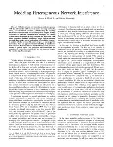
1. Introduction There is a strong demand in the market for fast and cheap development of reliable, standalone, wireless, multifunctional devices for automotive, aerospace and biomedical applications. Therefore the complexity of electronic sensors and multifunctional devices increases. Fast development of device fabrication technology stimulates new challenging technology development and progress in wafer processing, module interconnects and packaging technology. Apart from a broad hardware experience, standalone software design simulations have to be done before hardware fabrication. Such research and development work is done within the framework of e-Cubes [1] and SE2A [2] projects, where multimodule 3D integration of multifunctional elements is the main goal. Many various functionalities, such as power supply, power management, RF communication, digital signal processing, memory, micro electro-mechanical systems (MEMS) and many other have to be assembled into a single device. The range of applications is not limited to automotive, aerospace and biomedical domains only. As the device integration is an important factor of the design process in improving the reliability of the device, new materials, technologies and technological concepts are being tested and verified. The reliability of vertical interconnects turns out to be one of crucial design issues. Thermal management of the device and thermo-mechanical stress simulations are prime candidates for research on reliability. From the reliability point of view standalone functional module simulations are insufficient to find out whether the modules will work if assembled into a final stacked device or not due to some thermal interactions neglected during the design verification process. For example, if one module dissipates the power, the heat flows through VIA’s. It extends to other modules and affects thermal budget of other devices. A slightly different point of view is exploited within the Corona project [3], where the main goal is to develop the best methodology and tools for fast product development. 34
It should cover the whole flow from the idea to the final micro-nanotechnology product. The key issue is short time-to-market and efficient dataflow for distributed design and fabrication scenarios. One of the main goals of the Corona is also the support of the multi-site product development – where every module of the integrated microsystem may be fabricated in the best technology in different places/fabs and finally integrated into one multifunctional device (Fig. 1).
Fig. 1. Multi-site product development scenario, where every module of the integrated microsystem (MEMS+IC’s) may be fabricated in the best technology in different places/fabs and finally integrated into one multifunctional device.
From this point of view different design tools are important at different design stages: from device design, through device modeling and simulation, to process development and optimization. It enables fast virtual prototyping for selected parts of the device or the whole final device.
2. Multi-Domain Modeling and Simulation Examples As it has been mentioned before, multi-domain modeling and simulation is very important at every stage of device fabrication. Selected examples of various multi-domain modeling and simulation are presented. For design, modeling and simulations of heterogeneous micro- and nanostructures designers may use CoventorWare [4] and ESI-CFD [5] software environments implementing multi-domain FEM (finite element method) simulation and analysis of the micro- and nanostructures. One of the key reliability issues of 3D structures is the intercon-
Multi-Domain Modeling and Simulations of the Heterogeneous Systems
nection reliability. Several integration techniques have been considered within the framework of the e-Cubes project to obtain sample demonstrator structures. An example of the integrated modeling and simulation is shown in Fig. 2.
sure needed to be applied for thermo-compression bonding is also investigated.
Fig. 2. (a) SEM image of a group of microinserts [6], [7] and (b) 3D model of a quarter of a group of 9 microinserts in CoventorWare.
Thermo-electro-mechanical microinsert simulations [6], [7] have been performed (Figs. 3 and 4) to find the electrical and mechanical behavior of the simulated structures and to verify possible electromigration problems and assess the electrical suitability of the examined structures. The pres-
Fig. 3. Multi-domain simulation results: von Mises stress distribution across a microinsert structure under pressure of 1 MPa applied on top of the structure with single and multiple microinsert configurations (diameter of 1.5 m, height of 5 µ m and pitch of 3 µ m for multiple microinserts).
Fig. 4. Multi-domain simulation results: current density distribution through microinserts under 10 V applied between upper and bottom part.
The results presented in Figs. 3 and 4 show the von Mises stress distribution across the microinsert structure under the pressure of 1 MPa for device configurations with single and multiple microinserts. It is very important to characterize the stress distribution under different pressures according to thermo-compression bonding process usually used for 3D integration. The current density distribution shows how the current flows through the modeled 3D device. It also makes it possible to verify if one should expect such problems as, e.g., electromigration. Modeling and simulation results at this stage can help to optimize, e.g., geometry, materials and dimensions (e.g., diameter, pitch, height). Besides modeling and simulation efforts devoted to the single structure used for 3D integration, modeling and simulation of the integrated microsystem have been also presented. Such a system is the e-Cubes project demonstrator sample. The general idea of the project is presented in Fig. 5 [8]. From the reliability point of view thermo-mechanical behavior of the whole system is one of the most important 35
T. Bieniek, G. Janczyk, P. Janus, J. Szynka, P. Grabiec, A. Kociubiński, M. Ekwińska, D. Tomaszewski, and A. Malinowski
Also some mechanical issues regarding the encapsulation methodology were considered. Thermal simulations results show that under the assumed boundary conditions the temperature does not increase too much across the whole demonstrator device structure. Sample results of the thermal investigation are shown in Fig. 7.
Fig. 7. Temperature distribution through a 3D model of the integrated microsystem in two modes: (a) high power mode and (b) low power mode. Fig. 5. (a) Physical architecture of a sensor node (whole system for health monitoring), drawing not on scale [8] and (b) mechanical design drawing (3D model) [8].
reliability parameters. Even if all standalone modules are correctly designed, simulated and one can anticipate perfect operation after assembly process, in the case of 3D integration their functionality may be affected by various side effects not taken into consideration during the design process. Each of the assembled modules of a 3D multimodule device interferes thermally and electrically with its neighborhood (see Fig. 6). The probability that a single module may affect another by, e.g., high temperature transfer is quite high. Therefore the module arrangement and complex simulation are necessary at each design stage.
Analysis of the mechanical displacement simulation leads to a major conclusion. Displacement and stress distribution is better if more fixed points are applied to the device (Fig. 8). While in the high power mode the maximum displacement reaches 24 µ m on the edge of the structure, in the low power mode the displacement does not exceed 6 µ m.
Fig. 8. Mechanical part of multi-domain simulation and modeling results – displacement magnitude (displacement and deformation factor rescaled ×100!!!) of structures in high power mode in two different modes of fixation to the package.
Fig. 6. Interactions between microsystem modules [9].
The 3D integration technique has been simulated along with realistic thermo-mechanical boundary conditions applied (power dissipation from different modules and parts). 36
The heterogeneous device oriented (Hedoris) multi-domain simulation system [10], [11] will be developed within the framework of the projects mentioned above. The Hedoris system implements the idea of the hardware description language (HDL) of the device model based on VerilogAMS [12] language specification used for device thermal modeling. Currently the system is mainly optimized to run thermal simulations of heterogeneous devices and is still under development. Intensive work has been undertaken including TCAD simulations oriented on the system
Multi-Domain Modeling and Simulations of the Heterogeneous Systems
extension to cover thermo-mechanical internal device interactions, such as mechanical stress, which may affect the overall performance of the device.
3. Summary The design and verification methodologies are discussed and presented. Modeling and simulation samples presented in this paper show the importance of the flexibility of the multi-site design and development framework of cooperation. The paper also shows how universal CAD tools used for design of micro- and nanodevices in distributed engineering environments should be and how important it is to correctly estimate the device reliability and keep balance between reaching the attractive time to market and fulfilling the customer requirements.
Acknowledgements This work has been partially supported by the European Commission under support-number: IST-026461 (European project: 3D Integrated Micro/Nano Modules for Easily Adapted Application, acronym e-CUBES [1]), CP-FP 213969-2 (European project: Customer-Oriented Product Engineering of Micro and Nano Devices, acronym CORONA [2]) and Eniac SE2A (Nanoelectronics for Safe, Fuel Efficient and Environment Friendly Automotive Solutions [3]). We would like to thank e-Cubes and CORONA project Partners for the excellent and fruitful collaboration, special thanks to Ric van Doremalen and Piet van Engen from Philips Applied Technologies.
References [1] e-Cubes project, http://www.ecubes.org [2] Nanoelectronics for Safe, Fuel Efficient and Environment Friendly Automotive Solutions project, http://www.eniac.eu, SE2A [3] Corona project, http://www.corona-mnt.eu [4] 3D MEMS Design Automation and Virtual Fabrication – Coventor, http://www.coventor.com [5] ESI Group CFD Portal, http://www.esi-cfd.com/ [6] A. Mathewson, J. Brun, C. Puget, R. Franiatte, N. Sillon, F. Depoutot, and B. Dubois-Bonvalot, “Microstructured interconnections for high security systems”, in Proc. Electron. Syst. Integr. Technol. Conf., 2006, Dresden, Germany, vol. 1, pp. 126–132. [7] A. Mathewson, J. Brun, G. Ponthenier, R. Franiatte, A. Nowodzinski, N. Sillon, G. Poupon, F. Deputot, and B. Dubois-Bonvalot, “Detailed characterisation of Ni microinsert technology for flip chip die on wafer attachment”, in Proc. Electron. Compon. Technol. Conf. ECTC’07, Sparks, USA, 2007, pp. 616–621. [8] P. van Engen, R. van Doremalen, W. Jochems, A. Rommers, S. Cheng, A. Rydberg, T. Fritzsch, J. Wolf, W. De Raedt, P. Müller, E. Alarcon, and M. Sanduleanu, “3D Si-level integration in wireless sensor node”, in Proc. Smart Syst. Integr. 2009 Conf., Brussels, Belgium, 2009, pp. 150–157. [9] T. Bieniek, P. Janus, A. Kociubiński, P. Grabiec, G. Janczyk, and J. Szynka, “Integrated multi-domain modeling and simulation of complex 3D micro- and nanostructures”, in. Proc. Smart Syst. Integr. 2008, Barcelona, Spain, 2008, pp. 399–402.
[10] G. Janczyk, T. Bieniek, J. Szynka, and P. Grabiec, “Reliability issues of e-Cubes heterogeneous system integration”, Microelectron. Reliab., vol. 48, pp. 1133–1138, 2008. [11] G. Janczyk, T. Bieniek, J. Szynka, and P. Grabiec, “Integrated thermal modeling of heterogeneous eCubes stacked devices”, in Proc. Therminic 2008, 14th Int. Worksh. Thermal Invest. ICs Syst., Roma, Italy, 2008, pp. 80–84. [12] Accelera, “Verilog-AMS Language Reference Manual”, Version 2.1, 2003, http://www.accellera.com
Tomasz Bieniek received the M.Sc. and Ph.D. degrees in electronic engineering from the Warsaw University of Technology, Poland, in 2002 and 2007, respectively. The doctor thesis was devoted to plasma technologies for ultrathin dielectric layer formation. In 2006 he joined the Department of Silicon Microsystems and Nanostructure Technology of the Institute of Electron Technology, Warsaw. His research is focused on MEMS and CMOS silicon technologies and multi-domain modeling, as well as the simulation of micro- and nanostructures. He is an author and co-author of more than 40 technical papers and presentations presented in journals and at conferences. e-mail:
[email protected] Institute of Electron Technology Lotników av. 32/46 02-668 Warsaw, Poland Grzegorz Janczyk received the M.Sc. degree (with honors) and Ph.D. degree in electronic engineering from the Warsaw University of Technology (WUT), Poland, in 1999 and 2005, respectively. Since then, he has been with the Institute of Microelectronics and Optoelectronics (IMIO), VLSI Engineering and Design Automation Division, at the same university. In 2006 he joined the Institute of Electron Technology (ITE). He is an Assistant Professor in IMiO-WUT and ITE. His main Ph.D. related interests cover device modeling along with technological SOI fabrication process modeling and development of SOIMOS transistor models. Multi-domain device modeling using Verilog language also belongs to the range of his professional interests. Statistical yield simulations and mismatch modeling are secondary field of interest. He is also C++ programmer. e-mail:
[email protected] Institute of Electron Technology Lotników av. 32/46 02-668 Warsaw, Poland 37
T. Bieniek, G. Janczyk, P. Janus, J. Szynka, P. Grabiec, A. Kociubiński, M. Ekwińska, D. Tomaszewski, and A. Malinowski
Paweł Janus received the B.Sc. and M.Sc. degrees from the Technical University in Wrocław, Poland, in 1996 and 1998, respectively. In 2003 he received the Ph.D. degree in electrical engineering from the Wrocław University of Technology. Since 2003, he has been with the Institute of Electron Technology, Warsaw. His research interests include studies of materials for MEMS applications, micromachining of silicon microstructures, microsensors, and microactuators. His current research is silicon force sensors development for nanomechanical applications. He is an author and co-author of more than 30 technical papers presented in journals and at conferences. e-mail:
[email protected] Institute of Electron Technology Lotników av. 32/46 02-668 Warsaw, Poland Jerzy Szynka graduated in 1972 and received in 1976 the Ph.D. from Technical University Dresden, Germany. The doctor thesis was devoted to cellular automata theory. In 1977 he joined to the Institute of Mathematical Machines in Warsaw, Poland, where he worked on automation project. In 1978 he joined to the Institute of Electron Technology in Warsaw. In 1992 he became Managing Director in Quantum Ltd. the software company, where he was responsible for the development and application of commercial software. From 2002 he is the Head of the Circuit and System Department of Institute of Electron Technology managing the research and development on behavioral synthesis using VHDL and Verilog description languages, silicon implementation of algorithms and design of mixed signal ASICs. Actual activities concern the design methods for heterogeneous systems. e-mail:
[email protected] Institute of Electron Technology Lotników av. 32/46 02-668 Warsaw, Poland Piotr B. Grabiec graduated from the Warsaw University of Technology, Poland, in 1973, and received the Ph.D. degree in chemistry from the same university in 1985. In 1974 he joined the Institute of Electron Technology, Warsaw, where he was involved in CVD and diffusion technology research. Since 1999 he has been the Head of 38
Silicon Microsystem and Nanostructure Department. His present activity involves fabrication of silicon ASICs, optoelectronic devices and MEMS and their integration. He has been involved in 10 EU projects and has been awarded numerous awards for development and commercialization of advanced micro-devices. He is the member of IEEE and Electrochemical Society. He is the author and co-author of more than 300 scientific papers and conference presentations. He holds 19 patents. e-mail:
[email protected] Institute of Electron Technology Lotników av. 32/46 02-668 Warsaw, Poland
Andrzej Kociubiński received the M.Sc. and Ph.D. degrees in electronic engineering from the Warsaw University of Technology, Poland, in 2002 and 2007, respectively. In 2001 he joined the Department of Silicon Microsystems and Nanostructure Technology of the Institute of Electron Technology, Warsaw. Since 2007, he has been with the Lublin University of Technology. His research interests include diagnostics, characterization, simulation and modeling of silicon devices. His recent works are related to SOI devices, pixel detectors on SOI wafers and integrated microsystems. e-mail:
[email protected] Lublin University of Technology Nadbystrzycka st 38a 20-618 Lublin, Poland
Magdalena Aleksandra Ekwińska received the M.Sc. and Ph.D. degrees in micromechanics from the Warsaw University of Technology, Poland, in 2002 and 2009, respectively. The doctoral thesis was devoted to investigation of nanoscale material properties and comparison of two commonly used nanoscale tests: nanowear and nanoindentation. One of the results was the method of prediction of the results of the time consuming nanowear test based on the information from nanoindentation test only. In 2001 she was an Intern with Hysitron Company (manufacturer of nanoindentation equipment) and in 2003 with the Mechanical-Mathematical Department of the University of Belarus. From 2007 she is a member of Polish Tribology Society (PTT), which is a founder member of International Tribology Council (ITC). In 2008 she joined the Institute of Electron Technology to the Department of Silicon Microsystems and Nanostructure Technology.
Multi-Domain Modeling and Simulations of the Heterogeneous Systems
Her work is focused to MEMS multi-domain modeling and simulation of micro- and nanostructures. e-mail:
[email protected] Institute of Electron Technology Lotników av. 32/46 02-668 Warsaw, Poland Daniel Tomaszewski received the M.Sc. degree from the Warsaw University of Technology, Poland, in 1980. Since then he is with the Institute of Electron Technology, Warsaw. In 1998 he received the Ph.D. degree in electrical engineering. His research interests include modeling and characterization of silicon and silicon-on-insulator devices for the purpose of IC diagnostics and design. He participated in several conferences and workshops related to these fields. e-mail:
[email protected] Institute of Electron Technology Lotników av. 32/46 02-668 Warsaw, Poland
Arkadiusz Malinowski received the B.Sc. and M.Sc. degrees from the Warsaw University of Technology, Poland, in 2005 and 2007, respectively. He currently pursues the Ph.D. degree in electrical and computer engineering at the Warsaw University of Technology and the Nagoya University, Japan. In March 2004 he joined the Institute of Electron Technology, Warsaw, working in the area of TCAD semiconductor process and device simulation. His research interests include FinFET CMOS technology scaling, nanocarbon based FET and plasma nanoprocessing. Institute of Electron Technology Lotników av. 32/46 02-668 Warsaw, Poland e-mail: m
[email protected] Nagoya University C3-1 (631), Furo-cho, Chikusa-ku 464-8603 Nagoya, Japan
39