Surface Science 454â456 (2000) 1094â1098 www.elsevier.nl/locate/susc. Multi-technique application of a double reflection electron emission microscope.
Surface Science 454–456 (2000) 1094–1098 www.elsevier.nl/locate/susc
Multi-technique application of a double reflection electron emission microscope Krzysztof Grzelakowski 1 Focus GmbH, Am Birkhecker Berg 20, D65510 Hu¨nstetten-Go¨rsroth, Germany
Abstract Results obtained with the recently developed double reflection electron emission microscope applied in different imaging modes are presented. The novel illumination system is based on a (100)-oriented single crystalline W wire electron microreflector and an electron gun placed in the back focal plane of the immersion objective. After being elastically reflected from the W tip surface, the primary electrons of energy ranging from 1 to 6 keV are decelerated to the desired impact energy in the range 0 to 200 eV for mirror electron microscopy (MEM ), low energy electron emission microscopy (LEEM ) and low energy electron diffraction (LEED) modes or to 5 keV for the secondary electron imaging mode. Photoelectron emission microscopy (PEEM ), MEM, LEEM, secondary images of Pd/Si(111) and a set of selected area LEED patterns of the W(100) surface taken at energies ranging from 5 to 40 eV are presented for the first time. © 2000 Published by Elsevier Science B.V. All rights reserved. Keywords: Electron emission measurements; Electron microscopy; Low energy electron diffraction (LEED); Low-energy electron microscopy (LEEM )
1. Introduction Emission microscopy covers a wide range of imaging techniques that are characterized, in contrast to scanning techniques, by parallel image acquisition. This feature makes emission microscopy particularly attractive for the research of dynamic processes at surfaces [1]. Since the first electron emission micrographs were obtained in 1932 by Bru¨che and Johannson [2], a number of different techniques and instrumental setups have been employed [3]. As was successfully demonstrated with low energy electron emission microscopy (LEEM ) [4], reflection emission microscopy offers a richness of selective information about the 1 Permanent address: Uznamska 8, PL54-315 Wroclaw, Poland.
topography, crystalline [1] or magnetic [5,6 ] structure, and chemical composition [7]. The continuing development of reflection microscopy illustrates the significance of this technique for the research of surfaces [8,9]. The concept of the double reflection electron emission microscope (DREEM ) [10] permits the complementary exploitation of many contrast mechanisms and techniques {thermionic, secondary, Auger, mirror, diffraction, phase contrast, dark field, photoelectron emission microscopy (PEEM ), X-ray photoelectron emission microscopy ( XPEEM ), LEEM, spin polarized low energy electron microscopy (SPLEEM ), and standard surface science methods: low energy electron diffraction (LEED), and electron spectroscopy [Auger electron spectroscopy (AES), X-ray photoelectron spectroscopy ( XPS), and ultraviolet
0039-6028/00/$ - see front matter © 2000 Published by Elsevier Science B.V. All rights reserved. PII: S0 0 39 - 6 0 28 ( 00 ) 0 01 9 7 -7
K. Grzelakowski / Surface Science 454–456 (2000) 1094–1098
1095
photoelectron spectroscopy ( UPS)] when equipped with an energy analyzer [11]}. Some of the possible operating modes of the DREEM have already been proven and are presented in this paper. Since the prototype instrument is described elsewhere [10], only its electron optical configuration will be presented.
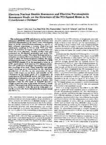
2. Electron optical configuration A key feature of the DREEM is the novel illumination system consisting of an electron microreflector [ W(100) single crystal wire] and an electron gun, both placed in the back focal plane of the immersion objective lens [10]. The e-gun is oriented and mounted perpendicular to the optical axis of the imaging column. The primary electron beam focused at the reflector (100) face specularly reflects and drifts along to the optical axis of the objective since the reflector is located under 45° in the field-free region of the objective lens. After being decelerated in the objective, the electron beam reaches the sample as a collimated bundle with energy e(V −V ), where V is the microscope M P M column potential and V is the negative potential P of the electron source. Since the sample is held at ground, the energy of the illuminating electrons is determined by the potential of the cathode only. That feature simplifies the operation of the instrument. Fig. 1a illustrates schematically the first order optics in the imaging mode. The collimated primary electron beam evenly illuminates the sample surface. If the sample is crystalline and the primary electron energy is low, then the backscattered electrons will create a LEED pattern in the back focal plane. Because of the cylindrical symmetry of the system, all secondary electrons will be distributed symmetrically around the (00) reflex. As seen in Fig. 1, the iris aperture is located exactly in the real image plane of the objective. In the imaging mode it is usually used as a field-of-view aperture. The transfer lens transfers the selected image by way of the iris aperture to the input of the first projective lens. To reach the highest magnification the second projective lens has to be activated, as shown in Fig. 1a. The contrast aperture (not shown in Fig. 1a) is mounted as close as possible to the microreflector. In the version with
Fig. 1. Schematic illustration of the imaging mode of DREEM ( left-hand side) and LEED mode of DREEM (right-hand side; for simplicity the electron gun is not drawn).
an energy analyzer, the aperture is to be transferred to the corresponding diffraction plane [11]. Fig. 1b illustrates the configuration of the instrument in the diffraction mode. The transfer lens and the first projective lens are the only two voltages that have to be changed in order to switch from imaging to LEED mode. As seen in Fig. 1b, the LEED pattern that appears on the screen corresponds to the real image cut off by the iris aperture. With the continuously adjustable aperture the arbitrary field of view of the sample between 3 and 500 mm can be selected for the LEED experiment. That feature of the iris aperture has already been applied in laterally resolved local measurements [12,13]. This will be particularly important for the DREEM equipped with an energy analyzer [11].
3. Contrast mechanisms in DREEM There are a number of different modes of operation possible with the DREEM; a few of them (PEEM, MEM, LEEM, secondary electron emission microscopy, and LEED) have recently been proven and are presented in this paper. The specimen, consisting of 1.5 mm wide palladium bars evaporated onto a Si(111) substrate, has been imaged in four different operating modes of the DREEM. The results are presented in Fig. 2. The PEEM image shown in Fig. 2a has been taken
1096
K. Grzelakowski / Surface Science 454–456 (2000) 1094–1098
Fig. 2. 1.5 mm wide palladium bars on silicon: (a) PEEM image, illumination from a high pressure mercury lamp; (b) mirror image; (c) LEEM image at 15 eV; (d) secondary electron image at 150 eV.
using illumination from a mercury discharge lamp with cut-off energy hn=4.9 eV. The lamp was oriented under an angle of 30° to the specimen surface. As a consequence, the right edge of the palladium bars becomes more intense than the other edge. The uncoated areas of silicon stay dark, as the photon energy does not exceed the threshold for the photoelectric emission. Because the value 4.9 eV lies just above the threshold for the electron emission from the palladium, the system is suitable to give high contrast. When the ultraviolet ( UV ) illumination of the specimen is not used and the electron gun is activated ( Fig. 1a), and depending on the impact energy of the primary electrons, different imaging modes and contrast mechanisms can be exploited. Fig. 2b shows the result of operating the DREEM in the mirror microscopy mode. The LaB cathode of the e-gun 6 is biased slightly below the potential of the specimen. The primary electrons are turned back before impacting the specimen surface (intense signal ), or they are absorbed if their energy is slightly higher (no signal ). The same mechanisms will lead to the high contrast of the micrograph when the impact energy is fixed and the local potential at the surface is distorted by charging effects and topography. As seen in Fig. 2b, the primary electrons are strongly reflected at the edges of the palladium bars and absorb without scattering near the flat areas of the specimen. Fig. 2c represents the case when the low energy elastically reflected electrons are chosen to visualize the surface. The cathode potential was kept at −15 V and the test specimen was grounded. In the back focal plane of the objective only a diffused specular spot has been registered (the test object could not be cleaned ). To increase the contrast, a 100 mm aperture has been placed on the axis to mask part of the diffuse specular reflex. The LEEM image taken using elastically backscattered electrons with an energy of 15 eV and 100 mm contrast aperture is shown in Fig. 2c. To explore the inelastic modes of the DREEM, the impact energy of the primary electrons has been increased to 150 eV. At higher impact energies, the contribution of the secondary electrons to the image rises. The differences in secondary emission coefficients of different substances are the source for the secondary electron contrast, the
K. Grzelakowski / Surface Science 454–456 (2000) 1094–1098
1097
same as used in scanning electron microscopy (SEM ). However, unlike SEM, DREEM uses the secondary electrons to form parallel rather than scanned micrographs. Since secondary electrons with different energies will be accepted by the immersion objective lens of the DREEM and propagate along the symmetry axis of the imaging column, the chromatic aberrations of the system will be detrimental to the lateral resolution, if no imaging filter is applied [11]. Fig. 2d shows the unfiltered secondary electron image taken at the primary electron energy of 150 eV. When using the immersion objective lens [14], the low energy electron diffraction technique used in the emission microscopes shows at least two important peculiarities compared with the retarding field LEED instruments: (1) the LEED pattern corresponds to a very small area of the specimen selected by the iris aperture; and (2) the location of diffraction spots in the pattern does not depend on the energy of the diffracted electrons. The first property is illustrated in Fig. 1b by means of first order optics. The second is derived from properties of the accelerating field of the immersion lens [15]. To explore the operation of the DREEM in LEED mode, a W(100) single face crystal replaced the standard test specimen. In Fig. 3 a set of diffraction patterns between 5 and 40 eV is shown. The iris aperture located in the first image plane has been reduced to the minimal size of 0.1 mm, that corresponds to the field of view of 3 mm, taking into account the magnification factor of the objective of 35. The electrons diffracted from outside the selected area do not contribute to the LEED pattern. An example of the (10) diffraction spot in Fig. 3b–d illustrates the fact that energy change influences only the intensity and not the position of reflexes.
4. Conclusions The goal of the present study is to examine the scientific utility of the double reflection electron emission microscope. Four different imaging modes (PEEM, mirror, LEEM and secondary electron microscopy) were tested using a Pd/Si(111) specimen. A set of LEED patterns of W(100) surface taken at different energies corresponding to the 3 mm large area of the surface
Fig. 3. Diffraction patterns of the W(100) at energies: (a) 5 eV; (b) 20 eV; (c) 30 eV; (d ) 40 eV.
illustrates the capability of the instrument for selected area measurements. Spectroscopic aspects of that feature of the instrument equipped with
1098
K. Grzelakowski / Surface Science 454–456 (2000) 1094–1098
the energy analyzer will be tested in the near future, as well as the capability of the instrument for imaging the magnetic structures.
Acknowledgements My thanks are due to G. Schoenhense and J. Kirschner for inspiring me to do the experiment. The author is also grateful to M. Merkel and M. Escher for discussions during the experiment and to Izabella Darda for critical reading of the manuscript.
References [1] W. Telieps, E. Bauer, Ultramicroscopy 17 (1985) 57. [2] E. Bru¨che, H. Johannson, Naturwissenschaften 20 (21) (1932) 353.
[3] O.H. Griffith, P.A. Habliston, G.B. Birrell, Ultramicroscopy 36 (1–3) (1991) 262. [4] E. Bauer, Phys. Rev. 123 (1961) 1206. [5] M.S. Altman, H. Pinkvos, J. Hurst, H. Poppa, G. Marx, E. Bauer, Proc. Mater. Res. Soc. 232 (1991) [6 ] K. Grzelakowski, T. Duden, E. Bauer, H. Poppa, S. Chiang, IEEE Trans. Magn. 30 (1994) 4500. [7] E. Bauer, T. Franz, Cz. Koziol, G. Lilienkamp, T. Schmidt, in: R. Rosei ( Ed.), Chemical, Structural and Electronic Analysis of Heterogeneous Surfaces on Nanometer Scale, Kluwer, Dordrecht, 1996. [8] O.H. Griffith, W. Engel, Ultramicroscopy 36 (1991) 1. [9] L.H. Veneklasen, Rev. Sci. Instrum. 63 (1992) 5513. [10] K. Grzelakowski, Rev. Sci. Instrum. 70 (1999) 3346. [11] K. Grzelakowski, in preparation. [12] K. Grzelakowski, Focus IS-PEEM, unpublished. [13] W. Swiech, G.H. Fecher, Ch. Ziethen, O. Schmidt, H.P. Oepen, G. Scho¨nhense, K. Grzelakowski, C.M. Schneider, R. Fro¨mter, J. Kirschner, J. Electron Spectrosc. Relat. Phenom. 84 (1997) 171. [14] A. Delong, V. Drahosˇ, Nature (London) Phys. Sci. 230 (1971) 196. [15] W. Telieps, Dissertation, TU Clausthal, 1983.