Mar 10, 2010 - Each rectifier at the transformer's secondary side has its own controller, therefore all of the output voltages can be regulated for the entire load ...
Multiple-output Class E Isolated dc-dc Converter Z. Pavlovic, J.A. Oliver, P. Alou, O. Garcia, R.Prieto, JA. Cobos Universidad Politécnica de Madrid Centro de Electrónica Industrial José Gutiérrez Abascal 2, 28006 Madrid
Abstract - This paper presents a multiple output class-E isolated dc-dc converter that regulates the output voltages at fixed switching frequency. The two output converter is simulated at operating frequency of 5 MHz. The converter output power is 40 W and the output voltages are 15 V and 5 V. All the switches operate at zero voltage switching (ZVS) conditions for the full load range. The circuit configuration is simple with small passive components which reduce the size of the converter. The circuit also has very good cross-regulation and an inherent short circuit protection with preserved ZVS conditions.
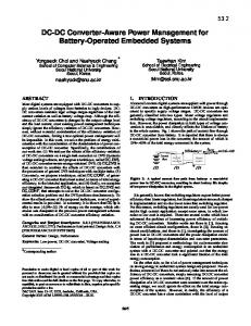
voltage at fixed switching frequency by controlling the conduction time of the auxiliary switch in the rectifier stage connected at the secondary side of the transformer. Based on this concept, in this paper we analyze the extension of this topology to the multiple output power supply, Fig. 2. Each rectifier at the transformer's secondary side has its own controller, therefore all of the output voltages can be regulated for the entire load range variations and the input line voltage variations. -TTfY\
I. INTRODUCTION Using high switching frequencies leads to a significant reduction of size of passive components. However, very fast voltage and current transitions mean increasing influence of the layout, the interconnections and packaging on the circuit behavior. Semiconductor devices are exposed to very high di/dt during commutations because of the energy stored in their parasitics which increase switching losses and electromagnetic interference and may cause breakdown of the device. Parasitic inductances and capacitances cause significant problems as the frequency of the circuit is increased. To address these problems in the design of highfrequency operating dc-dc converters topologies that incorporates these parasitics into circuit elements are a good alternative. The class-E resonant inverter topology, [l]-[5], addresses these problems which allow its operation in the megahertz order frequencies with zero-voltage switching and zerovoltage slope at turn-on if the switching conditions are met. The class-E topology also absorbs the power MOSFET's parasitic capacitance into the circuit elements and can be implemented with few components. These characteristics, in theory, allow achieving high power densities and high efficiency and reducing the size and weight of the converter. Since class-E inverter can operate at very high frequency with very high conversion efficiency it can be used in designing resonant dc-dc converters [6]-[10]. The isolated dcdc converter shown in Fig. 1, [11], [12], regulates the output This work has been supported by EADS Astrium CRISA
1|.
Fig. 1. The class-E isolated dc-dc converter
RFC
Lr
a
A8t
V..,
Cmlt'iJer
1
f.._
S4=tc
' • ' - • •
Fig. 2. Multiple output class-E isolated dc-dc converter
The analysis and evaluation of the impact that very high switching frequency has in multiple output power supplies is of special interest in the satellite applications. The launch cost is very high and there is a permanent interest in efficiency improvement and in the reduction of the mass and volume of the satellite's equipment. Switching at such a high frequency reduces significantly the size of the converter but can
increase the switching losses to an unacceptable level. In this sense, it is important to analyze topologies different to those ones used for lower frequencies (hundreds of kHz), [13]-[16], and to evaluate the reduction of converter's size when switching at high frequency. In this paper, the circuit operation is reviewed and the two output class E converter is designed and validated with PSpice simulation results. Basic circuit operation is also tested on a preliminary prototype. II.
deteriorating the converter's efficiency at low load.
D
-
CIRCIUT OPERATION
The multiple output class-E dc-dc converter shown in Fig. 2 consists of a class-E series resonant inverter at the primary side of a high frequency transformer and the controllable synchronous rectifiers at its secondary sides. The class-E inverter consists of a RF choke that injects a dc current into transistor's drain node, the switching transistor with a shunt capacitor and a series resonant tank with a high quality factor, Q, that makes the resonant tank current approximately sinusoidal. The transistor is driven with the signal at fixed switching frequency and fixed duty cycle. Zero voltage switching conditions, ZVS, are satisfied in both turn-on and turn-off and in the entire range of operation, from-full load to open-circuit. All the synchronous rectifier stages consist of one secondary winding of the transformer, the switching transistor with its parallel capacitor and the filter formed by the output capacitor and the load. Fig. 3 shows the rectifier model where the secondary winding is replaced with two current sources which represent the dc output current, that is magnetizing current IM, and the rectifier driving current, iAC. The principle of operation of the rectifier can be explained from the Fig. 4. The duty cycle D of the controlled switch is changing in the range of D^n < D < Dmax in order to regulate the output power at the desired level. When the transistor is off, the negative secondary current charges the parallel capacitor and the voltage VDS increases. The positive current discharges this capacitor, its voltage decreases, and at the time when its voltage crosses through zero the transistor is turned on. The averaged value of the voltage VDS is the output voltage since the averaged value of the transformer's secondary winding is zero. A change in the load resistance means changes in the currents IM and iAC and that leads to different negative peak of the transformer's secondary current and change the phase shift between the inverter's and synchronous rectifier's driving signal. Hence, the duty cycle D has to be changed to maintain the desired output power. The minimum value Dmin corresponds to the maximum output power when all the negative current is charging the shunt capacitor. In case of the short circuit at the output the duty cycle of the driving signal sets to the maximal value, Dmax, which is equal to 100 %. In this way the output current IM is equal to zero. The drawbacks of the topology are high circulating currents that increase as the load decreases
+
© '*•
/
A
Vnirr