NaNet: a Low-Latency, Real-Time, Multi-Standard Network Interface Card with GPUDirect Features
arXiv:1406.3568v1 [physics.ins-det] 13 Jun 2014
A. Lonardo∗ , F. Ameli∗ , R. Ammendola† , A. Biagioni∗ , O. Frezza∗ , G. Lamanna‡§ , F. Lo Cicero∗ , M. Martinelli∗ , C. Nicolau∗ , P. S. Paolucci∗ , E. Pastorelli∗ , L. Pontisso¶ , D. Rossettik , F. Simeone∗ , F. Simula∗ , M. Sozzi‡§ , L. Tosoratto∗ , and P. Vicini∗
Abstract—While the GPGPU paradigm is widely recognized as an effective approach to high performance computing, its adoption in low-latency, real-time systems is still in its early stages. Although GPUs typically show deterministic behaviour in terms of latency in executing computational kernels as soon as data is available in their internal memories, assessment of real-time features of a standard GPGPU system needs careful characterization of all subsystems along data stream path. The networking subsystem results in being the most critical one in terms of absolute value and fluctuations of its response latency. Our envisioned solution to this issue is NaNet, an FPGA-based PCIe Network Interface Card (NIC) design featuring a configurable and extensible set of network channels with direct access through GPUDirect to NVIDIA Fermi/Kepler GPU memories. NaNet design currently supports both standard - GbE (1000BASE-T) and 10-GbE (10Base-R) - and custom - 34 Gbps APElink and 2.5 Gbps deterministic latency KM3link - channels, but its modularity allows for a straightforward inclusion of other link technologies. To avoid host OS intervention on data stream and remove a possible source of jitter, the design includes a network/transport layer offload module with cycle-accurate, upper-bound latency, supporting UDP, KM3link Time Division Multiplexing and APElink protocols. After NaNet architecture description and its latency/bandwidth characterization for all supported links, two real world use cases will be presented: the GPU-based low level trigger for the RICH detector in NA62 experiment at CERN and the on-/off-shore data link for KM3 underwater neutrino telescope. Results of NaNet performances in both experiments will be reported and discussed.
I. NA N ET DESIGN OVERVIEW
N
ANET is a modular design of a low-latency PCIe RDMA NIC supporting different network links, namely standard GbE (1000BASE-T) and 10-GbE (10Base-R), besides custom 34 Gbps APElink [1] and 2.5 Gbps deterministic latency optical KM3link [2]. The design includes a network stack protocol offload engine yielding a very stable communication ∗ INFN Sezione di Roma, Italy. † INFN Sezione di Tor Vergata, Italy. ‡ INFN Sezione di Pisa, Italy. § CERN, Switzerland. ¶ Universit`a di Roma Sapienza, Dipartimento di Fisica, Italy. k NVIDIA Corporation, U.S.A. A. Lonardo is the corresponding author (
[email protected].) This work was supported in part by the EU Framework Programme 7 EURETILE project, grant number 247846; R. Ammendola was supported by MIUR (Italy) through the INFN SUMA project; G. Lamanna and M. Sozzi thank the GAP project, partially supported by MIUR under grant RBFR12JF2Z “Futuro in ricerca 2012”. Manuscript received May 22, 2014.
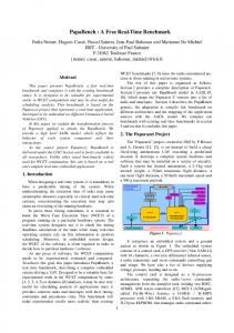
latency, a feature making NaNet suitable for use in real-time contexts; NaNet GPUDirect RDMA capability, inherited from the APEnet+ 3D torus NIC dedicated to HPC systems [3], extends its realtime-ness into the world of GPGPU heterogeneous computing. NaNet design is partitioned into 4 main modules: I/O Interface, Router, Network Interface and PCIe Core (see Fig. 1). I/O Interface module performs a 4-stages processing on the data stream: following the OSI Model, the Physical Link Coding stage implements, as the name suggests, the channel physical layer (e.g. 1000BASE-T) while the Protocol Manager stage handles, depending on the kind of channel, data/network/transport layers (e.g. Time Division Multiplexing or UDP); the Data Processing stage implements application dependent transformations on data streams (e.g. performing compression/decompression) while the APEnet Protocol Encoder performs protocol adaptation, encapsulating inbound payload data in APElink packet protocol, used in the inner NaNet logic, and decapsulating outbound APElink packets before re-encapsulating their payload in output channel transport protocol (e.g. UDP). The Router module supports a configurable number of ports implementing a full crossbar switch responsible for data routing and dispatch. Number and bit-width of the switch ports and the routing algorithm can each be defined by the user to automatically achieve a desired configuration. The Router block dynamically interconnects the ports and comprises a fully connected switch, plus routing and arbitration blocks managing multiple data flows @2.8 GB/s The Network Interface block acts on the trasmitting side by gathering data coming in from the PCIe port and forwarding them to the Router destination ports while on the receiving side it provides support for RDMA in communications involving both the host and the GPU (via the dedicated GPU I/O Accelerator module). A Nios II µcontroller in included to support configuration and runtime operations. Finally, the PCIe Core module is built upon a powerful commercial core from PLDA that sports a simplified but efficient backend interface and multiple DMA engines. As will be shown in the following, this general architecture has been specialized to be employed in several contexts, and implemented on several devices: Altera Stratix IV and V FPGA development kit and Terasic DE5-net board.
N/A
APEnet Proto Encoder
Link Ctrl
Decom pressor
NaNet Ctrl
BASE-R
TDM
UDP
N/A NaNet Ctrl
Decom pressor
NaNet Ctrl
NaNet-10 (10GbE)
Data Processing
UDP
10G
Det. Latency
KM3link
Word Stuff
NaNet-1 (GbE)
Protocol Manager
APElink
I/O Interface
TSE MAC
Physical Link APElink I/O IF Coding
Router TX/RX Block
32bit Micro Controller
Custom Logic
GPU I/O accelerator
memory controller
On Board Memory
Network Interface
PCIe X8 Gen2 core
Fig. 1.
NaNet architecture schematic.
II. NA N ET-1: A NIC FOR THE NA62 GPU- BASED LOW LEVEL TRIGGER
The NA62 experiment at CERN [4] aims at measuring the Branching Ratio of the ultra-rare decay of the charged Kaon into a pion and a neutrino-antineutrino pair. The NA62 goal is to collect ∼ 100 events with a signal to background ratio 10:1, using a novel technique with a high-energy (75 GeV) unseparated hadron beam decaying in flight. In order to manage the high-rate data stream due to a ∼ 10 MHz rate of particle decays illuminating the detectors, a set of trigger levels will have to reduce this rate by three orders of magnitude. The entire trigger chain works on the main digitized data stream [5]. The low-level trigger (L0), implemented in hardware by means of FPGAs on the readout boards, reduces the data stream by a factor 10 to meet the maximum design rate for event readout of 1 MHz. The upper trigger levels (L1 and L2) are software-implemented on a commodity PC farm for further reconstruction and event building. In the standard implementation, the FPGAs on the readout boards compute simple trigger primitives on the fly, such as hit multiplicities and rough hit patterns, which are then time-stamped and sent to a central processor for matching and trigger decision. Thus the maximum latency allowed for the synchronous L0 trigger is related to the maximum data storage time available on the data acquisition boards. For NA62 this value is up to 1 ms, in principle allowing use of more compute demanding implementations at this level, i.e. the GPUs. As a first example of GPU application in the NA62 trigger system we studied the possibility to reconstruct rings in the RICH. The RICH L0 trigger processor is a low-latency synchronous level and the possibility to use the GPU must be verified. In order to test feasibility and performances, as a
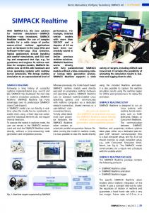
starting point 5 algorithms for single ring finding in a sparse matrix of 1000 points (centered on the PMs in the RICH spot) with 20 firing PMs (“hits”) on average have been implemented. Results of this study are available in [6] and show that GPU processing latency is stable and reproducible once data are available in the device internal memory. In order to fully characterize latency and throughput of the GPU-based RICH L0 trigger processor (GRL0TP), data communication between the detector readout boards (TEL62) and the L0 trigger processor (L0TP) need to be kept under control. The requisite on bandwidth is 400÷700 MB/s, depending on the final choice of the primitives data protocol which in turn depends on the amount of preprocessing actually to be implemented in the TEL62 FPGA. Therefore, in the final system 4÷6 GbE links will be used to extract primitives data from the readout board towards the L0TP. The NaNet-1 NIC was integrated in the GRL0TP prototype, using the “system loopback” setup described in section II-B. A. NaNet-1 implementation The NaNet-1 is a PCIe Gen2 x8 NIC featuring a standard GbE interface implemented on Altera Stratix IV FPGA Development Kit (see Fig. 2). A custom mezzanine mounting 3 QSFP+ connectors, was designed to be optionally mounted on top of the Altera board and makes NaNet-1 able to manage 3 bi-directional APElink channels with switching capabilities up to 34 Gbps. APElink adopts a proprietary data transmission word stuffing protocol; this is pulled for free into NaNet-1.
Fig. 2. NaNet-1 on Altera Stratix IV dev. board EP4SGX230KF40C2 with custom mezzanine card + 3 APElink channels.
The GbE transmission system follows the general I/O interface architecture description of Fig. 1. The Altera Triple Speed Ethernet Megacore (TSE MAC) is the Physical Link Coding, providing complete 10/100/1000 Mbps Ethernet IP modules. The UDP Offloader analyzes and interprets the data protocol. It deals with UDP packets payload extraction and provides a 32-bit wide channel achieving 6.4 Gbps which is a 6 times greater bandwidth than what the standard GbE requires. The data coming from TSE MAC are collected by the UDP Offloader through the Altera Avalon Streaming Interface and redirected into the NaNet hardware processing data
NaNet-1 APElink Communication + Kernel Latencies (M2070)
path, avoiding the use of the the FPGA on-board µcontroller (Nios II) from UDP traffic management. The NaNet Controller translates the UDP-encapsulated data packets into APEnet+ encapsulated ones, then hands them over to the Network Interface that takes care of moving them to their GPU memory buffer destination.
NaNet-1 performances were assessed on a Supermicro SuperServer 6016GT-TF. The setup comprised a X8DTG-DF (Tylersburg chipset — Intel 5520) dual socket motherboard, 2 Intel 82576 GbE ports and NVIDIA M2070 GPU; sockets were populated with Intel Xeon X5570 @2.93 GHz. The host simulates the RO board by sending UDP packets containing primitives data from the host system GbE port to the GbE port hosted by NaNet-1, which in turn streams data directly towards CLOPS in GPU memory that are sequentially consumed by the CUDA kernel implementing the ring reconstruction algorithm. This measurement setup is called “system loopback”. Exploiting the x86 Time Stamp Counter (TSC) register as a common time reference, it was possible in a single process test application to measure latency as time difference between when a received buffer is signalled to the application and the moment before the first UDP packet of a bunch (needed to fill the receive buffer) is sent through the host GbE port. Communication and kernel processing tasks were serialized in order to perform the measure; This represents a worst-case situation: given NaNet-1 RDMA capabilities, during normal operation this serialization does not occur and kernel processing seamlessly overlaps with data transfer. Similarly, we closed in a loopback configuration two of the three available APElink ports and performed the same measurement. NaNet-1 GbE Communication + Kernel Latencies (M2070)
2K 3000
Receive Buffer Size [Bytes] 8K 16K 32K 64K
128K
256K
Kernel Processing Latency (M2070) Total Latency NaNet-1 Communication Latency
2500
Latency [us]
4K
4K
8K
Receive Buffer Size [Bytes] 16K 32K 64K 128K 256K 512K
2000
1500
1000
500
0 16
32
64
128 256 512 1K 2K 4K Receive Buffer Size [Number of Events]
8K
compatibly with link bandwidth, low-latency on data transfers; for a more detailed performance analysis, see [7]. Bandwidth and latency performances for NaNet-1 APElink channel are in Fig. 4. It is clear that the system remains within the 1 ms time budget with GPU receive buffer sizes in the 128 ÷ 1024 events range. Although real system physical link and data protocol were used to show the real-time behaviour on NaNet-1, we measured on a reduced bandwidth single GbE port system that could not match the 10 MEvents/s experiment requirement for the GRL0TP. To demonstrate the suitability of NaNet-1 design for the full-fledged RICH L0TP, we decided to perform equivalent benchmarks using one of its APElink ports instead of the GbE one. Current implementation of APElink is able to sustain a data flow up to ∼ 20 Gbps. Results for latency of the APElink-fed RICH L0TP are shown in Fig. 4: a single NaNet-1 APElink data channel between RICH RO and GRL0TP systems roughly matches trigger throughput and latency requirements for receiving buffer size in the 4 ÷ 5 Kevents range. III. NA N ET3 : THE ON - SHORE READOUT AND SLOW- CONTROL BOARD FOR THE KM3N E T-IT
1500
UNDERWATER NEUTRINO TELESCOPE
500 0 16
32
64
128
256
512
1024
2048
4096
Receive Buffer Size [Number of Events]
Fig. 3. Latency of NaNet-1 GbE data transfer and of ring reconstruction CUDA kernel processing.
In Fig. 3 latencies for varying size buffer transfers in GPU memory using the GbE link are represented. Besides the smooth behaviour increasing receive buffer sizes, fluctuations are minimal, matching both constraints for real-time and,
16K
Fig. 4. Latency of NaNet-1 APElink data transfer and of ring reconstruction CUDA kernel processing.
2000
1000
1M
Kernel Processing Latency (M2070) Total Latency NaNet-1 APElink Communication Latency
2500
Latency [µs]
B. Results
2K
KM3NeT-IT is an underwater experimental apparatus for the detection of high energy neutrinos in the TeV÷PeV range ˇ based on the Cerenkov technique. ˇ The detector measures the visible Cerenkov photons induced by charged particles propagating in sea water at speed larger than that of light in the medium, and consists of an array of photomultipliers (PMT). The charged particle track can be reconstructed measuring ˇ the time of arrival of the Cerenkov photons on the PMTs, whose positions must be known. The KM3NeT-IT detection unit is called tower and consists of 14 floors vertically spaced 20 meters apart. The floor arms are about 8 m long and support 6 glass spheres called Optical Modules (OM): 2 OMs are located at each floor end and
2 OMs in the middle of the floor; each OM contains one 10 inches PMT and the front-end electronics needed to digitize the PMT signal, format and transmit the data. Each floor hosts also two hydrophones, used to reconstruct in real-time the OM position, and, where needed, oceanographic instrumentation to monitor site conditions relevant for the detector. All data produced by OMs, hydrophones, and instruments, are collected by an electronic board contained in a vessel at the centre of the floor; this board, called Floor Control Module (FCM) manages the communication between the on-shore laboratory and the underwater devices, also distributing the timing information and signals. Timing resolution is fundamental in track reconstruction, i.e. pointing accuracy in reconstructing the source position in the sky. An overall time resolution of about 3 ns yields an angular resolution of 0.1 degrees for neutrino energies greater than 1 TeV. Such resolution depends on electronics but also on position measurement of the OMs, which is, in fact, continuously tracked. The spatial accuracy required should be better than 40 cm. A. The KM3NeT-IT DAQ and data transport architecture The DAQ architecture is heavily influenced by the need of a common timing distributed all over the system in order to correlate signals from different parts of the apparatus with the required nanosecond resolution. The aim of the data acquisition and transport electronics is to label each signal with a “time stamp”, i.e. the hit arrival time, in order to reconstruct tracks. This need implies that the readout electronics, which is spatially distributed, require common timing and a known delay with respect to a fixed reference. The described constraints hinted to the choice of a synchronous link protocol which embeds clock and data with a deterministic latency; due to the distance between the apparatus and shoreland, the transmission medium is forced to be an optical fiber. All floor data produced by the OMs, the hydrophones and other devices used to monitor the apparatus status and the environmental conditions, are collected by the Floor Control Module (FCM) board, packed together and transmitted through the optical link. Each floor is independent from the others and is connected by an optical bidirectional virtual point-to-point connection to the on-shore laboratory. The data stream that a single floor delivers to shore has a rate of ∼300 Mbps, while the shore-to-underwater communication data rate is much lower, consisting only of slow-control data for the apparatus. To preserve optical power budget, the link speed is operated at 800 Mbps, which, using an 8B10B encoding, accounts for a 640 Mbps of user payload, well beyond experimental requirement. Each FCM needs an on-shore communication endpoint counterpart. The limited data rate per FCM compared with state-of-the-art link technologies led us to designing NaNet3 , an on-shore readout board able to manage multiple FCM data channels. This design represents a NaNet customization for the KM3NeT-IT experiment, adding support in its I/O interface for a synchronous link protocol with deterministic latency at physical level and for a Time Division Multiplexing protocol at data level (see Fig. 1).
B. NaNet3 implementation The first stage design for NaNet3 was implemented on an evaluation board from Terasic, the DE5-net board, which is based on Altera Stratix-V GX FPGA, supports up to 4 SFP+ channels and a PCIe x8 edge connector. The first constraint to be satisfied requires having a time delta with nanosecond precision between the wavefronts of three clocks: • the first clock is an on-shore reference one (typically coming from a GPS and redistributed by custom fanout boards) and is used for the optical link transmission from NaNet3 towards the underwater FCM; • the second clock is recovered from the incoming data stream by a CDR module at the receiving end of the FCM which uses it for sending its data payload from the apparatus back on-shore; 3 • a third clock is again recovered by NaNet while decoding this payload at the end of the loop. The link established in this way is fully synchronous. The second fundamental constraint is the deterministic latency that the Altera Stratix device must enforce — as the FCM does — on both forward and backward path to allow correct time stamping of events on the PMT. In this way, the NaNet3 board plays the role of a bridge between the 4 FCMs and the FCMServer — i.e. the hosting PC — through the PCIe bus. Control data en route to the underwater apparatus are correctly sent over the PCIe bus to the NaNet3 board, which then routes the data to the required optical link. On the opposite direction, both control and hydrophones data plus signals from the front-end boards are extracted from the optical link and re-routed on the PCIe bus towards an application managing all the data. Since the data rate supported by the PCIe bus is much higher than the data produced by the off-shore electronics, we foresee to develop a custom board supporting more than 4 optical links. On the other hand, the GPUDirect RDMA features of NaNet, fully imported in NaNet3 design, will allow us, at a later stage, to build an effective, real-time, GPU-based platform, in order to investigate improved trigger and data reconstruction algorithms. At a higher level, two systems handle the data that come from and go to off-shore: the Trigger System, which is in charge of analysing the data from PMTs extracting meaningful data from noise, and the so-called Data Manager, which controls the apparatus. The FCMServer communicates with these two systems using standard 10-GbE network links. C. The NaNet3 preliminary results Preliminary results show that the interoperability between different vendors FPGA devices can be achieved and the timing resolution complies with physics requirements. We develop a test setup to explore the fixed latency capabilities of a complete links chain. We leverage on the fixed latency native mode of the Altera transceivers and on the hardware fixed latency implementation for Xilinx device [8]. The testbed is composed by the NaNet3 board and the FCM Xilinx-based board respectively emulating
the on-shore and off-shore boards connected by optical fibers (see Fig. 5). The external GPS-equivalent clock has been input to the
Fig. 6. Deterministic latency feature of NaNet3 SerDes: the plot scope shows the phase alignment of the transmitting (purple) and receiving (yellow) parallel clocks after 12 h test of periodic reset and initialisation sequence.
IV. C ONCLUSIONS AND FUTURE WORK
Fig. 5.
NaNet3 testbed.
NaNet3 to clock the transmitting side of the device. A sequence of dummy parallel data are serialised, 8b/10b encoded and transmitted, together with the embedded serial clock, at a data rate of 800 Mbps along the fiber towards the receiver side of the FCM system. The FCM system recovers from the received clock and transmits the received data and recovered clock back to the NaNet3 boards. Lastly, the received side of NaNet3 deserializes data and produces the received clock. The way to test the fixed latency features of the SerDes hardware implementation is quite easy taking into account that every time a new initialisation sequence, following an hardware reset or a powerup of the SerDes hardware, has been done, we should be able to measure the same phase shift between transmitted and received clock, equal to the fixed number of serial clock cycles shift used to correctly align the deserialised data stream. Fig. 6 is a picture taken from scope acquisition in Infinity Persistence showing the results of a preliminary 12 h test where every 10 s a new reset and align procedure has been issued. The NaNet3 transmitter parallel clock (the purple signal) maintains exactly the same phase difference with the receiver parallel clock (the yellow signal) and with the FCM recovered clock (the green signal).
Our NaNet design proved to be efficient in performing real-time data communication between the NA62 RICH readout system and the GPU-based L0 trigger processor over a single GbE link. Preliminary results of its customization for the data transport system of the KM3NeT-IT experiment shows that the fundamental requirement of a deterministic latency link can be implemented using NaNet, paving the way to the use of hybrid trigger and data reconstruction systems. NaNet-10 10 GbE board, currently under development, will allow for a full integration of our architecture in the NA62 experiment and smooth the path to NaNet usage in other contexts. R EFERENCES [1] R. Ammendola, A. Biagioni, O. Frezza, A. Lonardo, F. L. Cicero, P. S. Paolucci, D. Rossetti, F. Simula, L. Tosoratto, and P. Vicini, APEnet+ 34 Gbps data transmission system and custom transmission logic, Journal of Instrumentation 8 (2013), no. 12 C12022. [2] A. Aloisio, F. Ameli, A. D’Amico, R. Giordano, V. Izzo, and F. Simeone, “The NEMO experiment data acquisition and timing distribution systems,” in Nuclear Science Symposium and Medical Imaging Conference (NSS/MIC), 2011 IEEE, Oct 2011, pp. 147–152. [3] R. Ammendola, A. Biagioni, O. Frezza, F. L. Cicero, A. Lonardo, P. S. Paolucci, D. Rossetti, F. Simula, L. Tosoratto, and P. Vicini, “APEnet+: a 3D Torus network optimized for GPU-based HPC systems,” Journal of Physics: Conference Series, vol. 396, no. 4, p. 042059, 2012. [Online]. Available: http://stacks.iop.org/1742-6596/396/i=4/a=042059 [4] G. Lamanna, “The NA62 experiment at CERN,” Journal of Physics: Conference Series, vol. 335, no. 1, p. 012071, 2011. [Online]. Available: http://stacks.iop.org/1742-6596/335/i=1/a=012071 [5] C. Avanzini et al., “The trigger and DAQ system for the NA62 experiment,” Nucl. Instrum. Methods Phys. Res., A, vol. 623, pp. 543– 545, 2010. [6] G. Collazuol, G. Lamanna, J. Pinzino, and M. S. Sozzi, “Fast online triggering in high-energy physics experiments using GPUs,” Nuclear Instruments and Methods in Physics Research A, vol. 662, pp. 49–54, Jan. 2012. [7] R. Ammendola, A. Biagioni, O. Frezza, G. Lamanna, A. Lonardo, F. L. Cicero, P. S. Paolucci, F. Pantaleo, D. Rossetti, F. Simula, M. Sozzi, L. Tosoratto, and P. Vicini, “Nanet: a flexible and configurable lowlatency nic for real-time trigger systems based on gpus,” Journal of Instrumentation, vol. 9, no. 02, p. C02023, 2014. [Online]. Available: http://stacks.iop.org/1748-0221/9/i=02/a=C02023
[8] R. Giordano and A. Aloisio, “Fixed latency multi-gigabit serial links with Xilinx FPGA,” IEEE Transaction On Nuclear Science, vol. 58, no. 1, pp. 194–201, 2011.