From July 2005 High Frequency Electronics Copyright © 2005 Summit Technical Media
High Frequency Design
OSCILLATOR DESIGN
Noise Reduction in Transistor Oscillators: Part 3—Noise Shifting Techniques By Andrei Grebennikov M/A-COM Eurotec
I
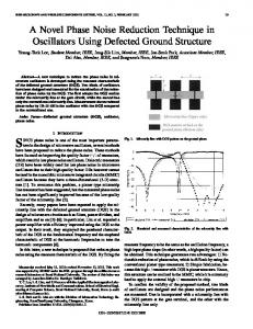
n modern wireless communication systems, cross-coupled oscillators have been preferred over other topologies for monolithic integrated circuit implementation because they are easily realized using CMOS technology and differential circuitry. However, because the current-source transistor is top or tail located, to improve the phase noise performance, it is necessary to use the special filtering techniques for second harmonic suppression. Therefore, the new oscillator topologies based on classical types of oscillators can overcome this problem when one of the active device ports is grounded [28]. In addition, these topologies provide larger oscillation amplitude for a given bias current because there is no voltage drop of the DC current across the current-source transistor, similar to the differential voltage-biased VCO shown in Figure 23. Figure 27(a) shows a single-ended common base bipolar Colpitts oscillator configuration. The required regeneration factor for the startup oscillation conditions can be chosen using a proper ratio of the feedback capacitances C1 and C2. To maximize the loaded quality factor of the resonant circuit, the choke inductance can be connected between the bias resistor Rbias and emitter. In CMOS implementation, the single-ended bipolar common base oscillator can be replaced by the schematic using nMOS device shown in Figure 27(b) with RF grounded gate and current source instead of bias resistor. Connecting two identical singleended oscillators, as shown in Figure 27(c), can provide the differential output. In a per-
This series concludes with discussions of additional noise reduction methods using circuit topology, matching and feedback.
28
High Frequency Electronics
Figure 27 · Single-ended and differential oscillator topologies.
fectly balanced circuit, identical sides carry 180° (out of phase) signals of equal magnitude. Consequently, there is a midpoint (the center node between C2 capacitances) where the signal magnitude is zero. For absolutely identical circuits in each balanced side, the difference between signal magnitudes becomes equal to zero in each midpoint (dotted line) referring as a virtual ground. Because of a push-pull operation, the DC current flows through each current-source
High Frequency Design
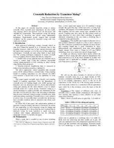
OSCILLATOR DESIGN transistors. In addition, the loaded quality factor of such an oscillator can be increased by connecting series inductances with a high reactance at the fundamental frequency between the main and cross-coupled transistors. The differential noiseshifting common gate VCO being fabricated using 0.35 µm BiCMOS process technology operates from 1.8 to 2.45 GHz [28]. The tank inductors have Q of 6. To maximize the oscillation voltage amplitude and Figure 29 · Bipolar cross-coupled dif- regeneration factor, the ferential VCO schematic. capacitance C2 was chosen to be four times capacitance C1. The oscillator shows a phase noise of –139 dBc/Hz at 3 MHz offset from the carrier of 1.8 GHz drawing DC current of 4 mA from a supply voltage of 2.5 V. The application of LC filtering technique to this oscillator when the added LC network was designed to resonate at second harmonic shows a negligible effect on the phase noise performance. To minimize the phase Figure 28 · Noise-shifting differential Figure 30. Bipolar balanced Colpitts noise of the cross-coupled common gate oscillator topologies. VCO schematic. differential VCO, it is necessary to optimize the capacitive feedback ratio as well. transistor during half a period. Therefore, these current Figure 29 shows the circuit schematic of the cross-coupled sources can be replaced by a pair of cross-coupled nMOS differential bipolar VCO designed for wireless application, transistors providing a synchronized current switching where L1 and L2 represent the parasitic bondwire inducfrom one side to another, as shown in Figure 28(a). To add tances, resistors R1 and R2 are used to damp the spurious frequency-tuning capability to the new oscillator topology, oscillations, capacitors C1, C2 and C3, C4 provide positive it is possible to include two varactors connected in paral- feedback [29]. The optimum feedback ratio for this design lel with the tank inductor. Finally, the two-shared C2 is C2/C1 = C4/C3 = 3.5. For a maximum varactor frequency capacitors connected in series can be replaced by an tuning bandwidth, the values of feedback capacitances equivalent capacitor with half of their value. The final dif- should be as small as possible. The optimization of the ferential noise-shifting common gate oscillator schematic feedback ratio is important to set operation conditions is shown in Figure 28(b) [28]. It should be noted that C2 with an optimum regeneration factor and symmetrical capacitances with virtual ground node serve as shunt waveforms of the collector current of each half-circuit as a capacitances used in the filtering technique. These capac- dominant noise contributor. For bipolar devices with fT = itances have small reactances at higher-order harmonics 25 GHz, its contribution at 100 kHz offset from the carriminimizing their magnitude through the current-source er of 800 MHz was of 68% of total noise, while the contri30
High Frequency Electronics
bution of the base resistance thermal noise was simulated to be less than 5%. Due to the loaded QL of the resonant circuit of about 16, the noise contribution from the resonator is 21%. Although the noise contribution from the tail current was sufficiently small, of about 7%, it becomes the major noise source at offset frequencies less than 3 kHz. The sum of all noise contributors results in the noiseto-signal ratio of –106.2 dBc/Hz. The VCO consumes 1.6 mA DC current from a 2.7 V supply. Figure 30 shows a balanced common gate Colpitts VCO fabricated using an InGaP/GaAs HBT process with fT = 60 GHz and fmax = 110 GHz [30]. By varying base bias voltage Vb from 2 to 3.5 V, it was found that there is an optimum value of approximately 3 V resulting in a minimum level of the phase noise and close to maximum tank voltage amplitude just before the onset of the transistor saturation. Such a critical operation mode corresponding to the border between the active and saturation regions provides a compromise conditions when the output power is high enough to minimize the phase noise level, but the collector-base junction has not been forward-biased yet to resistively shunt the oscillator resonant circuit making significantly worse its loaded quality factor. By varying varactor bias voltage Vv from 0 to 4 V, the frequency tuning of 150 MHz with output power of about 6 dBm with small variations within 1 dB was achieved. A minimum phase noise was less than –112 dBc/Hz at 100 kHz offset from the carrier of 6.4 GHz with the slope of 20 dB/decade at higher offsets.
Impedance Noise Matching It is known that to achieve maximum signal-to-noise ratio in oscillator, the optimum relationships between the active device, resonant circuit and feedback parameters should be established. For example, the minimum noise figure is obtained when the load conductance, also including the real part of the device output admittance, is transformed via feedback circuit into the optimum source admittance at the input of the active device. Therefore, generally for low-noise oscillator design, it is necessary to consider the following aspects [31]: • Proper choice of the active device with: · low noise figure combined with a small correlation coefficient · higher output power · low output conductance · reasonably high input impedance • Meeting an impedance condition at the input of the active device, which can be achieved by optimization of the feedback factor and which leads to optimum impedance noise matching • High quality factor of the resonant circuit • Optimum coupling coefficient of the feedback transformer
For example, by choosing the optimum value of the voltage transformation ratio of the transformer in a transformer-coupled oscillator, it is possible to improve the signal-to-noise ratio by 30 dB [31]. In a common case, it is difficult to satisfy all requirements simultaneously. In this case, the best signal-noise ratio can be achieved by optimization of the interdependent parameters. Considering the criteria for the choice of an optimum active element, sometimes it is much more promising to combine several active devices rather than using a single one. A low-noise input stage with sufficiently high input impedance is required, and a final stage with high output power capability and high output impedance. Figure 31 shows the simplified equivalent circuit of the transformer-coupled oscillator with dual-stage active element based on a tandem connection of the common source MESFET device with high input impedance and low noise figure and common base bipolar transistor with high output power capability. Compared with other transistor configurations, the common base connection shows the highest output impedance for the same output power. The minimum noise figure of the MESFET device is provided by optimum choice of the biasing conditions: drain supply voltage and DC current. To minimize the up-conversion of the 1/f noise, it is necessary to provide a nearly linear operation of the MESFET device. In addition, by appropriate partial coupling of the active element to the resonant circuit, the signal-to-noise ratio can be significantly improved. As an example, for a 150 MHz oscillator with the output power of –8 dBm, supply voltage of 35 V, DC current of 60 mA, coupling coefficient of 0.1 and quality factor of the resonant circuit of 300, the noise-to-carrier ratio (including both amplitude and phase noises) of –166 dBc measured in 1 Hz bandwidth at 10 kHz offset can be obtained with a 50 ohm load [31]. The cascode configuration of two bipolar devices, one with a common emitter and the other with a common base, gives a possibility to increase the output resistance of the active element resulting in higher loaded quality factor of the oscillator resonant circuit without degradation of the noise performance providing by the common emitter transistor. Figure 32 shows the circuit schematic of the cascode bipolar oscillator where the negative power supply is con-
Figure 31 · Equivalent circuit of optimally designed transformer-coupled oscillator. July 2005
31
High Frequency Design
OSCILLATOR DESIGN
Figure 32 · Bipolar cascode low-noise oscillator [32].
Figure 33 · Cascode VCO with optimum phase noise.
nected to the emitter of the first transistor, while the collector of the second transistor is DC grounded [32]. By using a low power bipolar device with fT = 3 GHz and a resonant circuit with quality factor Q0 = 200, an output power of 10 dBm at the oscillation frequency of 230 MHz with DC current of 6 mA and phase noise of less than –120 dBc/Hz at 10 kHz offset was obtained. In order to achieve a low level of the phase noise, it is very important to properly isolate the oscillator circuit from buffer amplifier using electric shielding. In addition, to minimize the effect of the board parasitics, the grounding of the circuit elements must be as close to each other as possible. Figure 33 shows a cascode bipolar VCO where the first transistor is connected in a common collector configuration, with the second transistor configured for common emitter operation [33]. The common collector device is used as a gain element and biased to operate in the active region by maximizing its quiescent current, preventing from going into saturation. If it were to saturate, it would load the tank circuit connected to its base terminal thus affecting the VCO phase noise performance. The common emitter transistor is used as limiting element providing the maximum VCO output power. Its partial connection to the tank circuit through the feedback capacitances C1, C2 and C3 is necessary to minimize the VCO phase noise. By optimizing the DC bias and RF feedback conditions, an improvement in 10 dB phase noise can be achieved without degrading the frequency tuning bandwidth. In the differential VCO, due to capacitive cross-coupling between the transistors, the resonant circuit is fully loaded on the equivalent input device impedance. However, if the gain capability of the active device is sufficiently high at the operating frequency, an optimum partial connection of the device into the resonant circuit can improve the noise performance and also gives a possibility to achieve higher signal amplitude while avoiding breakdown and keeping approximately the same tuning
range. Figure 34 shows the circuit schematic of the differential VCO with tapped resonant circuit inductor. As it can be expected, the phase noise will be reduced by 6 dB using a taping ratio 1:1. Being fabricated in a SiGe process, such a differential VCO using a tapped inductor, and the varactors represented by collector-base junctions with a hyperabrupt collector doping profile, provides a frequency tuning range of 23% around 2.4 GHz at a supply voltage of 2.5 V with current consumption of 16.5 mA and phase noise of –128 dBc/Hz at 1 MHz offset [34]. An additional active device can be used to compensate for the loss in the oscillation system. For example, by using the inverted common collector transistor configuration, a stable negative resistance is generated extracting the additional energy into the resonant circuit compensating for the loss due to the load resistance. This results in a significant increase in the loaded quality factor of the resonant circuit. Figure 35 shows the schematic diagrams of the oscillators (a) without compensation circuit and (b) with compensation circuit [35]. The soft start-up and steady-state oscillation conditions are realized by using the capacitive feedback reactance in the base and inductive reactances in the emitter and collector circuits. Both circuits have the same terminal impedances at the emitter and base ports, but different in the collector port. After incorporating the negative resis- Figure 34 · Differential tail-biastance circuit based on ed VCO with tapped inductor.
32
High Frequency Electronics
High Frequency Design
OSCILLATOR DESIGN
Figure 36 · Block diagram of microwave oscillator with nonlinear feedback loop.
monics and DC blocking capacitor. For the sake of the simplicity of an analytical representation, let us consider the only one low noise component. Then, the entire signal entering the nonlinear twoport network can be written by (22) Figure 35 · Schematic diagrams of oscillator (a) without and (b) with compensation circuit [35].
a common collector transistor VT2, the collector of the main transistor VT1 sees the inductive impedance with the resistive part approaching to zero. At the oscillation frequency of 800 MHz with output power of –6.8 dBm, the oscillator with compensation negative resistance circuit provides 6 dB phase noise improvement at 10 kHz offset.
Nonlinear Feedback Loop Noise Suppression [36] There is a real possibility to improve the oscillator phase noise significantly by using a special nonlinear feedback loop. Such a loop can create the proper phase conditions for output noise components, hich contribute to the subtraction of the noise components around the fundamental. Figure 36 shows a block diagram of ae microwave oscillator with an additional nonlinear feedback loop. The resonator can be represented by a filter or any configuration of lumped or distributed LC elements that can provide the proper conditions for the soft startup and steady-state oscillation conditions. An active device is shown as a noise-free nonlinear two-port network with a low noise voltage source connected to its input. A nonlinear feedback path includes diode as a nonlinear element, two matching circuits to match its input and output impedances, phase shifter, low-pass filter to suppress the fundamental, second and higher-order har34
High Frequency Electronics
where V0 is the DC bias voltage, Vin and ω are the voltage amplitude and frequency of the self-oscillations, V1/ƒ and Ω are the voltage amplitude and frequency of the low noise component with initial phase Φ, respectively. The transfer characteristic of the nonlinear two-port network can be represented by the power series of (23) where iout(t) is the output collector or drain current and vin(t) is the voltage at the active device input. For a polynomial representation of the transfer function, it is convenient to apply a power-series analysis, which is relatively easy to use and which gives a good intuitive sense of the nonlinear behavior of the active device. Substituting Eq. (22) into Eq. (23) and using trigonometric identities for the DC (constant), first (linear), second (quadratic) and third (cubic) voltage terms, we can write
(24)
High Frequency Design
OSCILLATOR DESIGN
where Ψ = Ωt + Φ. For the simplicity of numerical calculations, the values of a0 and V0 are considered zero, whereas the second and third orders of low noise voltage components, V21/ƒ and V31/ƒ are assumed to be negligible compared with others. It can be seen from Eq. (24) that the coefficients a1 and a3 have a significant effect on the amplitude of the fundamental component of the output current whereas the amplitudes of sidebands near the fundamental (ω + Ω and ω – Ω) are the functions of coefficient a2. By converting all components including the noise sidebands down to the baseband again through a properly set nonlinearity, we can obtain a signal identical, or very close to identical, to the signal that was produced by the original noise source. To properly design the feedback loop, it is necessary to provide the following experimental verification: • Nonlinear measurements for each coefficient, an • Choosing the elements for the power splitter and feedback LC filter for the particular oscillation frequency • Choosing a type of nonlinearity (proper active element in a nonlinear feedback loop) in accordance with values of the coefficients, an • Phase measurements to determine the proper phase shifter needed to achieve an inverted noise signal to add to the signal at the active device input. It is very important to make a correct choice of the nonlinear element in a nonlinear feedback loop for effective compensation of the noise components. The feedback signal from the nonlinear element can be written by (25) where iout(t) is the output collector or drain current defined by Eq. (24). According to Eq. (24), the new frequency components are produced as the mixing products of the terms appearing in Eq. (24). Consequently, it is necessary to investigate these products to be able to determine the required optimum values for coefficients bn. In this case, it is enough to take those products that contain less than second power of the voltage amplitude V1/ƒ representing low frequencies (since this signal is passed through a low-pass filter before entering the active device again). Figure 37 shows a diagram defining the feedback nonlinear coefficients b2 and b3 through a ratio of the active device transfer function coefficients a2/a3. Here, we can 38
High Frequency Electronics
Figure 37 · Feedback nonlinear coefficients b2 and b3 versus active device nonlinearity.
see that, for an active device with strong third-order nonlinearity when a2 a3 (when sidebands have sufficiently high amplitudes which is not typical), it is necessary to provide an active element with the strong second- and third-order nonlinearities at the same time, which cannot be effectively realized. The experimental verification was performed using a 5 GHz microstrip oscillator based on ATF36077 pHEMT device. For this type of a transistor, the gate-source capacitance and drain current source are the major contributors to the low frequency flicker noise, whereas the main nonlinearity is provided by a nonlinear transconductance. From the measured active device nonlinearity, it was found a value of 0.095 for the ratio of a2/a3. As a result, to provide a third-order nonlinearity in the feedback loop, the two diodes HSMS-8002 were connected in antiparallel position. The measured phase noise shows 5 dB improvement compared with 7 dB improvement obtained by simulation. This difference can be caused by the fact that the only noise source at the active device input was taken into account, and expected conversion loss in the feedback loop is higher. The major feature of this technique can be clearly seen from the simulation and measurement results: noise suppression effect is working over the entire noise bandwidth of interest, since the conversion and phase shift have constant value for all noise components through all over the frequency offset region (from kHz to MHz). Also, it is convenient in circuit implementation, as utilization (or later addition) of the low frequency feedback loop has a negligible effect on the amplitude and frequency of the selfoscillations. In addition, for a transistor configuration with common emitter, there is no need to use a phase shifter in the feedback loop since such a configuration
provides the required 180º phase inversion for the low frequency signal.
References 28. R. Aparicio and A. Hajimiri, “A Noise-Shifting Differential Colpitts VCO,” IEEE J. Solid-State Circuits, vol. SC-37, pp. 1728-1736, Dec. 2002. 29. M. A. Margarit, J. L. Tham, R. G. Meyer, and M. J. Deen, “A Low-Noise, Low-Power VCO with Automatic Amplitude Control for Wireless Applications,” IEEE J. Solid-State Circuits, vol. SC-34, pp. 761-771, June 1999. 30. H. Zirath, R. Kozhuharov, and M. Ferndahl, “A Balanced InGaP-GaAs Colpitts-VCO MMIC with UltraLow Phase Noise,” Proc. 12th Europ. GAAS Symp., pp. 3740, 2004. 31. G. Braun and H. Lindenmeier, “Transistor Oscillators with Impedance Noise Matching,” IEEE Trans. Microwave Theory Tech., vol. MTT-39, pp. 16021610, Sep. 1991. 32. A. S. Luchinin, “Low-Noise Bipolar Oscillator Design” (in Russian), Izvestiya Vuzov USSR, Ser. Radioelektronika, vol. 30, pp. 3-8, Mar. 1987. 33. J. K. McKinney, P. J. Yeh, and B. Avanic, “Cascode Oscillator Having Optimum Phase Noise and Bandwidth Performance,” U.S. Patent 5,621,362, Apr. 1997.
Millimeterwave Amplifiers
34. P. W. Lai, L. Dobos, and S. Long, “A 2.4 GHz SiGe Low Phase-Noise VCO Using On Chip Tapped Inductor,” Proc. 2003 Europ. Solid-State Circuits Conf., pp. 505-508. 35. V. M. T. Lam and P. C. L. Yip, “Microwave Oscillator Phase Noise Reduction Using Negative Resistance Compensation,” Electronics Lett., vol. 29, pp. 379-381, Feb. 1993. 36. T. Banky and T. Berceli, “Investigations on NoiseSuppression Effects of Nonlinear Feedback Loops in Microwave Oscillators,” 2004 IEEE MTT-S Int. Microwave Symp. Dig., pp. 2015-2018.
Author Information Andrei Grebennikov received the MSc degree in electronics from Moscow Institute of Physics and Technology, and the PhD degree in radio engineering from Moscow Technical University of Communications and Informatics, where he became a research assistant in the scientific and research department. From 1998 to 2001, he was a member of the technical staff at the Institute of Microelectronics, Singapore, and is now involved in the design of power amplifer modules and other products at M/A-COM Eurotec in Cork, Ireland. He can be reached by e-mail at: agrebennikov@tycoelectronics. com, or at
[email protected].