May 5, 2016 - achieved in heavily doped semiconductor nanoparticles (NPs) ... KEYWORDS: semiconductor plasmon nanoparticles, upconversion ...
Observation of Considerable Upconversion Enhancement Induced by Cu2−xS Plasmon Nanoparticles Donglei Zhou,† Dali Liu,† Wen Xu,*,†,‡ Ze Yin,† Xu Chen,† Pingwei Zhou,† Shaobo Cui,§ Zhanguo Chen,† and Hongwei Song*,† †
State Key Laboratory on Integrated Optoelectronics, College of Electronic Science and Engineering, Jilin University, 2699 Qianjin Street, Changchun, 130012, People’s Republic of China ‡ School of Chemical and Biomedical Engineering, Nanyang Technological University, 70 Nanyang Drive, Singapore 637457 § College of Physics, Jilin University, 2699 Qianjin Street, Changchun, 130012, People’s Republic of China S Supporting Information *
ABSTRACT: Localized surface plasmon resonances (LSPRs) are achieved in heavily doped semiconductor nanoparticles (NPs) with appreciable free carrier concentrations. In this paper, we present the photonic, electric, and photoelectric properties of plasmonic Cu2−xS NPs/films and the utilization of LSPRs generated from semiconductor NPs as near-infrared antennas to enhance the upconversion luminescence (UCL) of NaYF4:Yb3+,Er3+ NPs. Our results suggest that the LSPRs in Cu2−xS NPs originate from ligand-confined carriers and that a heat treatment resulted in the decomposition of ligands and oxidation of Cu2−xS NPs; these effects led to a decrease of the Cu2+/Cu+ ratio, which in turn resulted in the broadening, decrease in intensity, and red-shift of the LSPRs. In the presence of a MoO3 spacer, the UCL intensity of NaYF4:Yb3+,Er3+ NPs was substantially improved and exhibited extraordinary power-dependent behavior because of the energy band structure of the Cu2−xS semiconductor. These findings provide insights into the nature of LSPR in semiconductors and their interaction with nearby emitters and highlight the possible application of LSPR in photonic and photoelectric devices. KEYWORDS: semiconductor plasmon nanoparticles, upconversion luminescence enhancement, broadening, decrease and red-shift of LSPRs, electron injection
L
realization of LSPR and quantum-confined excitons within the same structure, opening the possibility of strong coupling of photonic to electronic modes, with implications for light harvesting, nonlinear optics, and quantum information processing.9,10 However, the basic features of the relationships between the structures, compositions, electronic structures, and optical properties of semiconductor NPs remain poorly understood. In this regime, Cu2−xE (E = S, Se, or Te) NPs are p-type semiconductors because of their copper deficiency, resulting in a large number of highly mobile hole carriers that support a strong LSPR in the near-infrared.1,11,12 At resonance, the electric field near the surface of a plasmon nanoparticle is strongly enhanced, resulting in molecules in the vicinity exhibiting altered light harvesting and emission.13,14 LSPR-induced luminescence enhancement based on various
ocalized surface plasmon resonance (LSPR) in heavily doped semiconductor nanoparticles (NPs, 5−11 nm) and in quantum dots (QDs, 2−4 nm) has attracted considerable interest since its discovery because of the unique optical properties and application potential of these materials in various photonic devices.1−3 In NPs composed of a noble metal such as gold or silver, LSPR originates from collective oscillations of excess free carriers, resulting in enhanced and tunable absorption and scattering resonances.4,5 The plasmonic behavior of semiconductor NPs is commonly considered to arise from collective oscillations of excess free carriers associated with constitutional vacancies or ionized dopant impurities in the lattice, leading to intense extinction bands at near-infrared (NIR) wavelengths.6,7 The LSPR in a semiconductor NP is unique because the LSPR energy can be tuned via doping or stoichiometry of the NP, providing an additional means of tuning the optical properties that is not as readily available in metals.8 Achievement of LSPR by free carrier doping of semiconductor NPs would enable active on-chip control of LSPR responses. Furthermore, NPs enable the © 2016 American Chemical Society
Received: January 26, 2016 Accepted: May 5, 2016 Published: May 5, 2016 5169
DOI: 10.1021/acsnano.6b00649 ACS Nano 2016, 10, 5169−5179
Article
www.acsnano.org
Article
ACS Nano
Figure 1. Schematic illustration and characterization on structure, morphology, and composition of various Cu2−xS NPs and Cu2−xS-MoO3NaYF4:Yb3+,Er3+ hybrid film. (a) Schematic illustration of the Cu2−xS-MoO3-NaYF4 hybrid structure. (b) XRD patterns of Cu2−xS film and Cu2−xS-MoO3-NaYF4:Yb3+,Er3+ hybrid film. (c−g) TEM images of Cu2−xS NPs with different sizes. Scale bar: 50 nm. (h) HR-TEM image of Cu2−xS NPs. (i) EDX spectra of Cu2−xS NPs with different sizes.
MoO3 spacer (0−16 nm) was deposited onto the Cu2−xS layer using the vacuum vapor deposition method. Finally, a NaYF4 layer with an approximate thickness of 150 nm was deposited on the top of the MoO3 (see Figure S1). Figure 1b−i show the structure, morphology, and composition of various Cu2−xS NPs and Cu2−xS-MoO3-NaYF4:Yb3+,Er3+ hybrid films. Four X-ray diffraction (XRD) peaks were observed in the XRD patterns of the Cu2−xS NPs, located at 27.8°, 32.2°, 46.2°, and 54.7°. These peaks were indexed to the (0,0,15), (1,0,10), (0,1,20), and (1,1,15) planes, respectively, of rhombohedral Cu2−x S (digenite) with space group R3̅m (JCPDS No. 47-1748). In the XRD pattern of the Cu2−xS-MoO3-NaYF4:Yb3+,Er3+ hybrid film, peaks originating from both rhombohedral Cu2−xS and cubic NaYF4 are evident, indicating the formation of a hybrid structure. Note that in the pattern of the hybrid film no peaks attributable to MoO3 were observed because of its low thickness (see Figure 1b). The transmission electron microscope (TEM) images imply that the Cu2−xS NP products are monodispersed, homogeneous, and sphere-like. The average sizes of the NPs are 6.5, 7.8, 8.8, 9.8, and 10.8 nm. The HRTEM image of Cu2−xS NPs in Figure 1h clearly shows that in a given particle the lattice is arranged along a single direction and that the lattice fringes have an interplanar spacing of 0.32 nm, which corresponds to the (0,0,15) spacing of rhombohedralphase Cu2−xS. To obtain the elemental compositions of the resulting samples, we analyzed various Cu2−xS NPs using quantitative energy-dispersive X-ray spectroscopy (EDX). As shown in Figure 1i, the atomic ratio of Cu to S increases linearly in the range from 1.75 to 1.91 with decreasing Cu2−xS particle size. X-ray photoelectron spectroscopy (XPS) spectra were also recorded to confirm the elemental compositions of the resulting samples (see Figure S2). The results indicate the coexistence of Cu+ and Cu2+ in the Cu2−xS NPs. The atomic ratios of Cu to S were determined to be 1.87, 1.83, and 1.71 for
metal nanostructures has been observed in various emitters (including dye molecules, quantum dots, and rare-earth (RE) ions) and has been applied to various photonic and photoelectric devices and to single-molecule detection.15,16 Recently, researchers have exploited the LSPR of some noblemetal nanostructures to enhance the near-infrared-to-visible upconversion luminescence (UCL) of RE-doped upconversion nanoparticles (UCNPs); the results of these studies demonstrate unique nonlinear emission features and considerable potential applications (ranging from bioapplications to photoelectric devices) of these materials.17,18 The challenge of effectively improving the UCL strength/efficiency19 of REdoped UCNPs has been a bottleneck in the implementation of various applications of UCL. The discovery of LSPR in heavily doped semiconductor NPs has opened a new regime in plasmonics1,20−22 and could provide an approach for improving the UCL of RE-doped UCNPs. In this paper, we report our observation of considerably enhanced UCL in a semiconductor-based LSPR device, Cu2−xSMoO3-NaYF4:Yb3+,Er3+, and discuss the physical characteristics of LSPR in Cu2−xS NPs and the nature of the interaction of LSPRs with the NaYF4:Yb3+,Er3+ UCNPs.
RESULTS Characterization of the Structure, Morphology, and Composition. A schematic of the Cu2−xS-MoO3-NaYF4:Yb3+,Er3+ hybrid structure is shown in Figure 1a. To prepare these hybrids, we prepared colloidal p-type Cu2−xS NPs with tunable LSPRs via the hot-injection method.8,23,24 We then spin-coated them onto a glass surface to serve as NIR nanoantennas; the thickness of the NP layer was fixed at approximately 900 nm. In an attempt to prevent the possible energy transfer (ET) from NaYF4:Yb3+,Er3+ UCNPs to Cu2−xS NPs and provide an appropriate interaction distance, a tunable 5170
DOI: 10.1021/acsnano.6b00649 ACS Nano 2016, 10, 5169−5179
Article
ACS Nano
Figure 2. Optical, electric, photothermal, and photoelectronic properties of the Cu2−xS NPs and Cu2−xS-MoO3-NaYF4 hybrids. (a) LSPR absorption spectra of Cu2−xS NPs with different sizes (6.5−10.8 nm) as dispersed in cyclohexane solutions. Dashed lines show trends in changes in LSPR peak values. (b) Temperature-dependent optical properties: LSPR absorption spectra of Cu2−xS film at different temperatures. When the sample was heated for about 2 min to reach the target temperature, the absorption spectrum was measured immediately. (c) LSPR absorption spectra of Cu2−xS film after 2 h thermal treatment under different temperatures. Inset: Calculated density of free carriers with respect to temperature. (d) Electric properties of Cu2−xS film: the temperature-dependent conductance. (e) Powerdependent LSPR absorption: LSPR absorption spectra of Cu2−xS film with 980 nm light irradiation at various power densities. Inset: Schematic of power-dependent LSPR absorption measurement. (f) Dependence of photoconductivity of the annealed Cu2−xS film on the irradiation power density of 980 nm light. The Cu2−xS film was annealed at 400 °C for 2 h. Inset: Schematic of conductivity measurement.
6.5, 8.8, and 10.8 nm Cu2−xS NPs, respectively; these results match well with the EDX analysis results (2% error). Optical, Electric, Photothermal, and Photoelectronic Properties. Before photoluminescence measurements, the optical, electric, photothermal, and photoelectronic properties of the Cu2−xS NPs and Cu2−xS-MoO3-NaYF4 hybrids were systemically studied to deeply understand the essence of LSPRs in semiconductor Cu2−xS NPs and their interaction with NaYF 4 :Yb 3+ ,Er 3+ UCNPs. Figure 2a shows the LSPR absorption spectra of Cu2−xS NPs of different sizes (6.5−10.8 nm) dispersed in cyclohexane solutions. A broad band extending from the visible to the NIR range was observed in the spectra of all the Cu2−xS NPs, and the peak wavelength gradually shifted toward the red with decreasing Cu2−xS particle size; this behavior is attributed to the decrease of the carrier density. In the case of the spectrum of the 10.8 nm Cu2−xS NPs, the LSPR peak is located at approximately 1000 nm, matching well the wavelength of the pumping light of UCL. Note that in the spectra of the Cu2−xS films or Cu2−xS-MoO3NaYF4 films the location of the LSPR peak was shifted approximately 40 nm toward the red (Figure S3), which we attributed to the coupling of different LSPR modes of Cu2−xS NPs. Based on the modified Mie−Drude theory by Luther et al.,1 the LSPR absorption frequency ωsp depends on the density of charge carriers (Nh), which can be expressed as
Nh =
ε0mh (1 + 2εm)(ωsp2 + γ 2) e2
(1)
where εm is the dielectric constant of the environmental medium; e is the elemental charge; ε0 is the free-space permittivity; m h is the hole effective mass, which is approximated to be 0.8m0 where m0 is the electron mass;22 and γ is the full-width at half-maximum of the LSPR-related absorption peak. Nh is the density of the free carriers. On the basis of eq 1, the values of Nh were determined to be 3.1 × 10²¹, 3.8 × 10²¹, 4.1 × 10²¹, 4.7 × 10²¹, and 5.3 × 1021 cm−3 for the 6.5, 7.8, 8.8, 9.8, and 10.8 nm Cu2−xS NPs, respectively. For comparison, Ne in gold is 5.9 × 1022 cm−3. Next, the Cu-to-S ratios for the 6.5, 7.8, 8.8, 9.8, and 10.8 nm Cu2−xS NPs were estimated to be 1.86, 1.83, 1.82, 1.79, and 1.76, respectively (see Note S1), which matched well with the EDX analysis and the XPS measurement (2.7% in error). To determine the free carrier density of Cu2−xS NPs, we performed Hall effect measurements (Figure S4). The results show that the Cu2−xS NPs were p-type semiconductor materials with a free carrier density of 1.55 × 1018 cm−3, which is 3 orders lower than the charge density required for generating LSPR (1021 cm−3). To further investigate this point, the FTIR and Raman spectra of the samples were collected (Figure S5). The results indicate that the as-prepared Cu2−xS NPs were wrapped with extra oleylamine (OAm) as surface ligands, which functioned as a surfactant solvent during the synthesis process. In fact, the insulated OAm ligands on the surface of Cu2−xS NPs confined 5171
DOI: 10.1021/acsnano.6b00649 ACS Nano 2016, 10, 5169−5179
Article
ACS Nano
S7). The XPS and EDX spectra were also collected; the results indicate that after annealing, the proportion of Cu2+/Cu+ decreased. Meanwhile, a peak associated with lattice oxygen was observed in the XPS spectra of annealed Cu2−xS, whereas only adsorbed oxygen was detected in the case of as-prepared Cu2−xS. This appearance of lattice oxygen indicates that oxidation indeed occurred during annealing, resulting in oxygen in the crystal lattice of Cu2−xS (Figure S8). Therefore, we conclude that oxidation occurred during the annealing process, leading to the observed decrease of the Cu2+/Cu+ ratio and to the red-shift of the peaks in the LSPR spectra of the annealed Cu2−xS nanoparticles. Notably, self-purification might also occur in Cu2−xS nanoparticles, which would further contribute to the decrease of the Cu2+/Cu+ ratio.28,29 Figure 2d shows the temperature dependence of the conductivity σ of the Cu2−xS film. In the measurement, the sample temperature was increased quickly; thus, the removal of ligands in the Cu2−xS film could be neglected. As evident in Figure 2d, the conductivity increases dramatically and exponentially with increasing temperature over the studied temperature range. As is well known, σ = neμ, where e is the charge quantity, μ is the charge mobility, and n is the charge density. In the high-temperature region, the variation of carrier mobility with temperature can be ignored in contrast to the exponential increase of charge density with temperature.28 Therefore, the dependence of the conductivity of the Cu2−xS film on temperature can be expressed as follows:
the migration of charge carriers from one Cu2−xS NP to another, leading to the lower carrier mobility. Therefore, the difference between the calculated carrier density and that determined by Hall measurements was mainly caused by the insulated ligands on the surface of the particles, which resulted in a low carrier mobility. The Hall effect measurement indicated that the charge carriers for generating the LSPR were confined inside the Cu2−xS nanocrystals by the OAm ligands, which could not move freely among the particles. Figure 2b shows the temperature-dependent LSPR of the Cu2−xS film consisting of 10.8 nm NPs after the sample was heated for approximately 2 min to reach the target temperature and then measured immediately. The results show that with increasing temperature the LSPR of the Cu2−xS NPs gradually red-shifted and broadened and that the absorption strength gradually decreased. The broadening of the LSPR for Cu2−xS NPs is attributed to the enhancement of electron−phonon coupling. To demonstrate this point, we studied the temporal dynamics of the relative differential transmission (ΔT/T) probed at 900 nm with a pump pulse wavelength of 1200 nm (Figure S6). In the dynamics measurements, the fast decay of the differential transmission that occurs within a few picoseconds is related to the coupling of electrons and phonons. The damping time induced by the coupling of the electrons and phonons decreases with increasing temperature, indicating that the broadening of plasmonic resonance is mainly induced by the coupling of electrons and phonons. A similar result has been reported for Cu2−xSe plasmon NPs.25 The red-shift of the LSPR peak with temperature is attributable to two possible causes: the variation of ε with temperature and the density change of charge carriers. According to the theoretical calculations reported by Scotognella et al.,25 the variation of LSPR induced by the change of ε is negligible in the studied temperature range.25 The density change of charge carriers may originate from two factors: lattice expansion with increasing temperature and a decrease of the number of holes, which is dominated by the Cu2+/Cu+ ratio. The lattice expansion coefficient for Cu2S is approximately 28.6 × 10⁻⁶ K−1.26,27 When the temperature varied from room temperature to 200 °C, the lattice expansion was only approximately 0.5%; lattice expansion therefore only slightly influenced the position of the LSPR peak. It is suggested that the chemical reaction on the surface of NPs is the main mechanism leading to the significant decrease of the hole density with increasing temperature. As previously discussed, the Cu2−xS nanoparticles were packed by oxygen-containing organic groups. When the temperature was increased, the organic groups decomposed, generating O2, which could react with sulfur on the surface of the particles, resulting in the loss of sulfur and a decrease of Cu2+/Cu+. To further investigate the reaction on the surface of the NPs, we subjected the Cu2−xS films to thermal treatments. In the experiments, each Cu2−xS film was heated for 2 h at a certain temperature under the protection of nitrogen and was then cooled to room temperature for its LSPR spectrum to be collected again. The LSPR properties of the Cu2−xS films after the thermal treatment are displayed in Figure 2c. After the annealing process, the LSPR bands gradually shifted to red and decreased substantially in intensity. When the films were annealed at temperatures greater than 200 °C, the LSPR bands disappeared completely. To evaluate the structural change, the XRD patterns of the annealed Cu2−xS NPs were collected; these patterns revealed a shift of 0.3−0.5° toward smaller angles, indicating that slight lattice expansion occurred (Figure
σ(T ) = σ0 exp( −ΔE /kT )
(2)
where σ(T) is the conductivity at any temperature, σ0 is the conductivity at 0 K, ΔE is the energy gap between the valence band and the indirect band gap of Cu2−xS NPs, k is the Boltzmann constant, and T is the absolute temperature. On the basis of eq 2, we deduced the values of ΔE to be 1.31, 1.29, 1.23, 1.18, and 1.14 eV, corresponding to the 6.5, 7.8, 8.8, 9.8, and 10.8 nm Cu2−xS samples, respectively. These deduced values are generally consistent with the indirect band gap of Cu2S estimated by optical measurements, and the gradual increase of ΔE with decreasing particle size is attributable to the quantum confinement effect.29,30 To evaluate the influence of the organic groups on the conductivity of Cu2−xS particles, we annealed the Cu2−xS films at 400 °C for 2 h under a nitrogen atmosphere and then measured the temperature dependence of their conductivity. The results indicated that the conductivity of Cu2−xS films after the thermal treatment increased by approximately 104 times compared to the conductivity of the as-prepared Cu2−xS films, whereas the slopes in the temperature−conductivity plots changed only slightly (Figure S9). Therefore, we concluded that the surface ligands strongly influenced the carrier mobility and σ0, but only slightly affected the temperature dependence of σ. After the annealing process, ΔE was almost independent of the Cu 2−xS NP size, which we attributed to the disappearance of the confinement effect due to the removal of ligands. To further elucidate the relationship between the optical and electric properties of the Cu2−xS plasmon NPs, the 980 nm light-irradiation-induced LSPR spectral change and conductivity change were investigated, as shown in Figure 2e and f, respectively. Figure 2e shows that upon irradiation with 980 nm light, the position of the LSPR absorption band gradually shifted to the red and the absorption intensity decreased. This observation is attributed to the temperature increase of the 5172
DOI: 10.1021/acsnano.6b00649 ACS Nano 2016, 10, 5169−5179
Article
ACS Nano
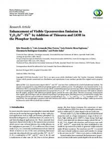
Figure 3. Comparison of the UCL enhancement between Au and semiconductor samples. (a) Schematic illustration of the fluorescence measurement methods. (b) Emission spectra excitated with 0.15 and 1.23 W/mm2 power, respectively. (c) Comparison of the UCL enhancement factors (EFs) of different transitions between Au-MoO3-NaYF4:Yb3+,Er3+ and Cu2−xS-MoO3-NaYF4:Yb3+,Er3+. (d) Power density dependence of integral UCL intensity of NaYF4:Yb3+,Er3+, Au-MoO3-NaYF4:Yb3+,Er3+ and Cu2−xS-MoO3-NaYF4:Yb3+,Er3+ (4S3/2/2H11/2−4I15/2 transitions). (e) Enhancement factors of Cu2−xS-MoO3-NaYF4 and Au-MoO3-NaYF4 film as a function of excitation power density. (f) Enhancement factor for 8 nm size and different thicknesses of MoO3 at 0.15 and 1.23 W/mm2 excitation power, respectively. (g) Dependence of EF on particle size of Cu2−xS NPs as well as the location of the LSPR band.
Cu2−xS films under irradiation with 980 nm light, resulting in oxidation at the surface of Cu2−xS NPs and a decrease of the Cu2+/Cu+ ratio. Figure 2f displays the dependence of photoconductivity of the annealed Cu2−xS films under 30 MPa pressure on the irradiation power density of 980 nm light. Note that after the Cu2−xS NPs were annealed at 400 °C for 2 h the ligands on their surface disappeared completely. As shown in Figure 2f, when the power density was less than 0.6 W/mm2, the conductivity slowly increased with increasing excitation power density (slope = 0.06). When the power density exceeded 0.6 W/mm2, the conductivity increased quickly, with a slope of 2.21 in the ln−ln plot, indicating that the conductivity was approximately proportional to the square of power density. This result provides evidence that at a high excitation power density of 980 nm light (1.26 eV) the electrons within the valence band of a Cu2−xS film can be pumped into the direct conduction band via a two-photon process. The direct band gap of 10.8 nm Cu2−xS NPs determined by optical measurement is approximately 2.4 eV, matching well with twice the energy of a 980 nm photon.31 In the presence of a large amount of ligands, although the band-to-band excitation via the twophoton process could still occur, the carriers would not be allowed to hop freely across the ligand barriers from one particle to the next. However, under irradiation by strong 980 nm light, the temperature of the Cu2−xS film would increase considerably (Figure S10), leading to the removal of some of the ligands on the surface of the Cu2−xS NPs; therefore, the
migration of carriers is likely to occur from one particle to another. UCL Enhancement of Cu2−xS-MoO3-NaYF4:Yb3+,Er3+ Hybrid Films. We were excited to observe that in the presence of a suitable amount of MoO3 the UCL of Er3+ in a Cu2−xS-MoO3-NaYF4:Yb3+,Er3+ hybrid film was greatly improved compared to that in the corresponding NaYF4:Yb3+,Er3+ film on a glass substrate. Moreover, we compared the Cu2−xSinduced UCL enhancement with metal-plasmon-nanostructure (Au-MoO3-NaYF4:Yb3+,Er3+)-induced enhancement; the results show that the interaction of NaYF4:Yb3+,Er3+ UCNPs with Cu2−xS NPs differed dramatically from that with the metal nanostructure. The preparation and characterization of Au nanorods and Au film are shown in Figure S11. Note that the comparison was performed under strict conditions, including the same laser source, the same excitation power density, and the same optical circuit (Figure 3a). In addition, the density of NaYF 4 :Yb 3+ ,Er 3+ UCNPs in the Cu 2−x S-MoO 3 -NaYF4:Yb3+,Er3+ hybrid film and in the NaYF4:Yb3+,Er3+ film are approximately the same, as determined by the optical properties of the NaYF4:Yb3+,Er3+ layer (Figure S1). Figure 3b shows a comparison of the normalized UCL spectra for a NaYF4:Yb3+,Er3+ film, a Cu2−xS-MoO3 (8 nm)NaYF4:Yb3+,Er3+ hybrid film, and a Cu2−xS-MoO3(8 nm)NaYF4:Yb3+,Er3+ hybrid film. In the spectra, blue 2H9/2−4I15/2, green 2H11/2/4S3/2−4I15/2, and red 4F9/2−4I15/2 transitions are observed. The populating of the blue 2H9/2 level is a threephoton ET process, whereas those for the green 2H11/2/4S3/2 and red 4F9/2 levels are both two-photon ET processes.32 In the 5173
DOI: 10.1021/acsnano.6b00649 ACS Nano 2016, 10, 5169−5179
Article
ACS Nano Cu 2 − x S-MoO 3 -NaYF 4 :Yb 3 + ,Er 3 + and Au-MoO 3 -NaYF4:Yb3+,Er3+ hybrids, the intensity ratios of 2H11/2−4I15/2 to 4 S3/2−4I15/2 both increase in comparison to that in the NaYF4:Yb3+,Er3+ nanofilm, indicating an increased temperature in the two samples.19,33,34 This increased temperature is due to the extra LSPR absorption and photothermal effect induced by the Cu2−xS and Au nanofilms. Interestingly, the variation of the intensity ratio of green 2H11/2, 4S3/2−4I15/2 to red 4F9/2−4I15/2 (G/R) in the two hybrid samples is opposite. The G/R in the Au-MoO3-NaYF4:Yb3+,Er3+ hybrid decreases, whereas that in the Cu2−xS-MoO3-NaYF4:Yb3+,Er3+ hybrid increases compared to that in the NaYF4:Yb3+,Er3+ film. In the Cu2−xS-MoO3NaYF4:Yb3+,Er3+ and Au-MoO3-NaYF4:Yb3+,Er3+ hybrids, the overall UCL intensity and the UCL intensities of different transitions all increase in contrast to those in the NaYF4:Yb3+,Er3+ film. Figure 3c shows a comparison of the UCL enhancement factors (EFs) of different transitions between Au-MoO3-NaYF4:Yb3+,Er3+ and Cu2−xS-MoO3-NaYF4:Yb3+,Er3+. Here, EF is defined as the UCL intensity ratio of Cu2−xS-based or Au-based hybrid films to that of the NaYF4:Yb3+,Er3+ film under the same conditions. On the basis of Figure 3b, we concluded that (1) the EF of the red emission is higher than that of the green emission for the Aubased hybrid, whereas the EF of the green is higher than that of the red for the Cu2−xS-based hybrid, and (2) under relatively weak excitation power density, the EF for the Cu2−xS-based hybrid is smaller, whereas at relatively high excitation power density, EF for the Cu2−xS-based hybrid is larger. To further study these phenomena, we compared the UCL intensity as a function of excitation power in different samples, as shown in Figure 3d (green emissions) and Figure S12 (blue and red emissions). As evident in the ln−ln plot (IUCL ∝ Pn), the slope n for the green emission in the NaYF4:Yb3+,Er3+ film is approximately 2; that is, two photons are required to populate the green level. In the case of the Au-based hybrid, in the starting range the slope deviates from 2, which is attributed to the saturation effect and the local thermal effect.35 The saturation effect depends on the competition between linear decay and UC processes for the depletion of the intermediate excited states, resulting in the deviation of n from the required photon number. The local thermal effect originates from the sample absorption of excitation light and the subsequent photothermal conversion, leading to a local temperature increase of the irradiated sample and luminescence quenching. As the excitation exceeds 0.7 W/mm2, the UCL even decreases with increasing excitation power due to temperature quenching. Similar to the Au-based hybrid, the slope n in the case of the Cu2−xS-based hybrid also deviates from 2 in the starting power range. Surprisingly, as the power density exceeds 0.7 W/mm2, the slope dramatically increases to 7.0, similar to the photon avalanche phenomenon.36 This increase in slope results in an unusual power-dependence of EF (Figure 3e). For the Aubased hybrid, similar to the results of previous literature reports, the EF decreases solely with increasing temperature, which is mainly attributed to the influence of the saturation effect and a local thermal effect.35 In the case of the Cu2−xS-based hybrid, the EF initially decreases with increasing temperature and approaches a minimum at approximately 0.6 W/mm2. Beyond this value, the EF gradually increases with increasing excitation power. This result suggests that the enhancement mechanism for the Cu2−xS-based hybrids may differ from that for the Aubased hybrid, as will be further discussed in the following text.
We note that in the aforementioned experiments, an 8 nm MoO3 spacing layer was used in the Au- and Cu2−xS-based hybrids to effectively enhance the UCL of NaYF4:Yb3+,Er3+. In fact, in the case of the Cu2−xS-MoO3-NaYF4:Yb3+,Er3+ hybrids, the EF also depends strongly on the thickness of the MoO3 spacer (Figure 3f). For the sample without an MoO3 layer, a slight decrease in UCL was observed, which might be related to the nonradiative ET from NaYF4:Yb3+,Er3+ to Cu2−xS. An enhancement of the UCL was observed with the assistance of the MoO3 spacer, and the optimal enhancement occurred when the thickness of the MoO3 layer was 8 nm; the enhancements were 82-fold at 1.23 W/mm2 and 8-fold at 0.15 W/mm2 for the Au- and Cu2−xS-based hybrids, respectively. A further increase of the MoO3 thickness led to a decrease of the EF. This result indicates that the effective interaction distance of plasmon Cu2−xS NPs is approximately 8 nm. To further demonstrate the essential interaction between the plasmon Cu2−xS NPs and NaYF4:Yb3+,Er3+ UCNPs, the dependences of EF on the particle size of Cu2−xS NPs and on the position of the LSPR band are shown in Figure 3g. At a power density of 0.15 W/mm2, the EF increases rapidly with increasing size of the Cu2−xS NPs and the LSPR band shifting toward the excitation wavelength. However, at 1.23 W/mm2, the EF exhibits only a slight increase with increasing size of the Cu2−xS NPs and blue-shifting of the LSPR band. This result definitely reveals that at relatively low power density the UCL enhancement originates mainly from the coupling of UCNPs with the LSPR of Cu2−xS NPs. At high excitation power, the UCL enhancement might be independent of the interaction of UCNPs with the LSPR. To demonstrate this point, the UCL enhancement in the annealed Cu2−xS-MoO3-NaYF4:Yb3+,Er3+ hybrid was studied. After the Cu2−xS NPs were annealed at 400 °C for 2 h, the LSPR of Cu2−xS NPs disappeared completely with the removal of the ligands. In this case, the UCL enhancement nearly disappeared at lower excitation power densities, whereas it remained almost unchanged at higher power densities (Figure S13). These results confirm that the UCL enhancement mechanism for the Cu2−xS-MoO3-NaYF4:Yb3+,Er3+ hybrid is power-dependent. UCL Dynamics of Au- and Cu2−xS-Based Hybrid Samples. In general, the LSPR-induced luminescence enhancement in the vicinity of plasmon NPs can be classified into two aspects: (1) the interaction of the LSPR with the emission electromagnetic field, resulting in the improved radiative transition rate of emitters; (2) the interaction of the LSPR with the excitation electromagnetic field, leading to an enhancement of the localized excitation field strength. Figure 4 shows the UCL dynamics of 2H9/2, 4S3/2, and 4F9/2−4I15/2 transitions of different samples. In the Cu2−xS-based and Aubased hybrids, the luminescent lifetimes for these transitions decrease in comparison to those in the NaYF4:Yb3+,Er3+ nanofilm, which implies an improvement of the total spontaneous transition rates for these transitions, including radiative and nonradiative ones. However, although the steadystate UCL for Er3+ increases to several 10’s times, the spontaneous rate for the corresponding transition increases by only up to 15%. This result indicates that in the Cu2−xSbased and Au-based hybrids the UCL enhancement results mainly from the interaction of LSPR with the excitation electromagnetic field, rather than from the interaction of LSPR with the emission electromagnetic field. In the vicinity of metal nanostructures, a significant increase of the radiative rate is frequently observed in dye 5174
DOI: 10.1021/acsnano.6b00649 ACS Nano 2016, 10, 5169−5179
Article
ACS Nano
Figure 4. UCL dynamics of Au and semiconductor samples. (a) Decay time of 2 H 9/2 ,4 S3/2 , and 4 F 9/2 − 4 I 15/2 transitions of NaYF4:Yb3+,Er3+ NCNPs under 980 nm excitation separated from Cu2−xS NPs as a function of MoO3 spacer layer. (b) Decay time of 2 H9/2,4S3/2, and 4F9/2−4I15/2 transitions of NaYF4:Yb3+,Er3+ NCNPs on different substrates.
molecules,37,38 whereas in the RE-doped UCNPs, the variation of the radiative rate was typically unnoticeable. This result is attributable to the following two facts. First, the interaction distance between dye molecules and the plasmon nanostructure is easier to control than that between the UCNPs and the plasmon nanostructure. In the UCNPs, some luminescence centers are located within the effective distance (