On-Chip Lookup Tables for Fast Symmetric-Key Encryption. A. Murat Fiskiran and Ruby ...... Dedicated instructions to accelerate table lookups in symmetric-key ...
On-Chip Lookup Tables for Fast Symmetric-Key Encryption A. Murat Fiskiran and Ruby B. Lee Princeton Architecture Laboratory for Multimedia and Security (PALMS) Department of Electrical Engineering, Princeton University {fiskiran, rblee}@princeton.edu
Abstract On public communication networks such as the Internet, data confidentiality can be provided by symmetric-key ciphers. One of the most common operations used in symmetric-key ciphers are table lookups. These frequently constitute the largest fraction of the execution time when the ciphers are implemented using a typical RISC-like instruction set. To accelerate these table lookups, we describe a new hardware module, called PTLU (for Parallel Table Lookup), which consists of multiple lookup tables that can be accessed in parallel. A novel combinational circuit included in the module can optionally perform simple logic operations on the data read from the tables. On a single-issue 64-bit RISC processor, PTLU provides maximum speedups of 7.7× for AES and 5.4× for DES. With wordsize scaling, PTLU speedups are significantly higher than that available through more conventional architectural techniques such as superscalar or VLIW execution.
1. Introduction Symmetric-key cryptography can be used to provide data confidentiality [18] on public communication networks such as the Internet. This involves encrypting a plaintext message P using a symmetric-key algorithm (cipher) and a secret key K. The encrypted message (ciphertext) is then sent to the receiver, where it is decrypted using the same cipher and secret key. Symmetric-key ciphers usually have an iterated round structure, where a short sequence of operations (called a round) is repeated on the plaintext block to compute the ciphertext [18]. The input of a round consists of the output of the previous round and one or more subkeys, which are derived from the secret key. Common round operations include table lookups, This work is supported in part by NSF CCR-0326372 and by DoD.
modular addition (subtraction), logical operations, shifts, rotates, multiplication, and bit permutations [18][22]. On a programmable processor that implements a RISC-like instruction set, table lookups generally consume the greatest fraction of the execution time [8]. In this paper, we describe how these can be accelerated cost-effectively with a new Parallel Table Lookup (PTLU) Module. The rest of the paper is organized as follows. In Section 2, we study the workload characteristics of six representative symmetric-key ciphers. Section 3 describes the PTLU hardware and Section 4 discusses its area cost and cycle time impact. In Section 5, we discuss the performance of PTLU. Section 6 reviews the related past work and Section 7 is the conclusion.
2. Cipher suite Table 1 lists the symmetric-key ciphers we selected for this study. For each cipher, we show the block size, typical key size, and the number of rounds. Block size is the amount of data that the cipher can encrypt at a time, and key size relates to the strength of the cipher against cryptanalytic attacks [18]. Data Encryption Standard (DES) [18] and its variant 3DES were the NIST standards for block encryption from 1976 to 2001. 3DES continues to be used extensively in many systems. RC4 is a popular stream cipher [18], which is originally used in the IEEE 802.11 wireless standard. Blowfish [18] is used in many protocols and applications, for example GPG, SSH, SSLeay, and JAVA cryptography extensions [19]. Advanced Encryption Standard (AES) [1] is the current NIST standard for block encryption. Its key size can be 128, 192, or 256 bits. We denote these AES-128, AES-192, and AES-256 respectively. Twofish [21] and MARS [5] are two of the five finalist ciphers in the AES selection program [2]. Together with AES, these new ciphers can be said to represent the current thinking in symmetric-key cipher design.
Proc. IEEE 16th Int. Conf. Application-Specific Systems, Architectures, and Processors (ASAP), pp. 356-363, Jul. 2005.
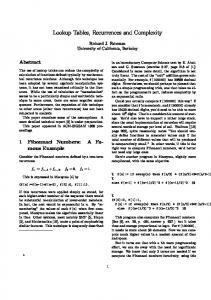
128 bits W3i
W2i b8
TA
TA
TB
64 64 8 64 128 128 128 128 128
56 112 128 128 128 192 256 128 128
16 48 1* 16 10 12 14 16 32
8 8 1 4 4 4 4 4 2
26 × 32 128 26 × 32 384 28 × 8 3 + 2W 28 × 32 64 28 × 32 160 28 × 32 192 28 × 32 224 28 × 32 128 28 × 32 80
b6
W0i
b5
b4
b2
b1
b0
TA
TA TB
TC
TD
TA[b8]
16 Table Lookups
TC
TD
TA[b12]
b3
TB
TC
TD
* RC4 does not have an iterated round structure; hence we show the number of rounds as 1. To generate each byte of keystream, RC4 requires 3 table reads and 2 writes.
b7
TB
TC
DES 3DES RC4 Blowfish AES-128 AES-192 AES-256 Twofish MARS
W1i
b15 b14 b13 b12 b11 b10 b9
Num. Lookups
Table Structure
Num. Tables
Num. Rounds
Key Size (bits)
Cipher
Block Size (bits)
Table 1: Cipher suite
TD
TA[b4]
TA[b0]
TB[b13]
TB[b9]
TB[b5]
TB[b1]
TC[b14]
TC[b10]
TC[b6]
TC[b2]
TD[b15]
TD[b11]
TD[b7]
TD[b3]
k[4i + 3]
k[4i + 2]
k[4i + 1]
k[4i + 0]
Load 4 subkeys XOR TLU results and subkeys
XOR
XOR
XOR
XOR
W3i+1
W2i+1
W1i+1
W0i+1
Figure 1: AES round Table 2: Instruction set
Register File
Class
Instructions add, addi, sub, subi, and, andi, or, ALU ori, xor, xori, not, loadi Shift sra, srai, srl, srli, sll, slli, shrp (shift right pair) Multiply mul.lo, mul.hi Memory load, store (base+displacement addressing) Branch beq, bne, bg, bge, call, return, trap New ISA ptrd.x, ptrd.s, ptw1, ptwn, byte_perm
64
Base ISA
ALU
Shifter
Multiplier
64
Figure 2: Baseline 64-bit single-issue processor
% Execution Cycles Spent in ..
Table 3: Breakdown of cipher execution time Block size (bits) Cycles per block
DES 64 1147
3DES 64 3384
RC4 8 18
Blowfish 64 408
AES-128 128 870
AES-192 128 1056
Table Lookups Arithmetic Logical Multiplication Fixed shift/rotate Variable rotate Bit permutation Other
38 21 8 26 7
44 24 9 15 8
54 14 26 6
36 26 34 4
72 24 4
72 24 4
2.1. Table lookups in symmetric-key ciphers We show the AES round structure in Figure 1 to illustrate how table lookups are typically used in symmetric-key ciphers. In Table 1, we also summarize the number and structure of the lookup tables used by each cipher. The notation 2a × b is used to denote a table with 2a entries, where each entry is b-bits wide.
AES-256 Twofish 128 128 1272 1753 72 24 4
43 15 32 4 6
MARS 128 1677 34 10 18 19 5 8 6
In AES, the input to the ith round is a 128-bit block composed of four 32-bit words. The bytes in these words are labeled b0 to b15. There are four 28×32 tables, labeled TA-TD. The rightmost byte of each word is used as index into TA; the next byte is used as index into TB; and so on, until all tables are accessed four times. The table lookup results and four subkeys are then exclusive-or’ed (XORed) as shown.
Of the remaining ciphers in our suite, Blowfish, MARS, and Twofish are similar to AES in that they use multiple 28×32 tables. DES and 3DES use eight 26 × 32 tables [18], while RC4 uses a single 28×8 table. In the next section, we measure the fraction of the execution cycles that each cipher spends in table lookups.
2.2. Execution time analysis We use the PLX toolset [13][17] to perform workload analysis of each cipher. For baseline performance data, the ciphers are implemented using the RISC-like instruction set shown as the Base ISA in Table 2. Our assembly code follows the optimizations described in [10] and [18]. We configure the simulator to model the 64-bit single-issue processor shown in Figure 2. All instructions execute in a single cycle except multiplication, which has a 3-cycle latency. We also assume a perfect memory with single-cycle load/store instructions. Table 3 shows the simulation results, which includes: (a) the execution cycles used per block of encryption, (b) the round operations in each cipher, and (c) the fraction of the execution time consumed by these. Our data presented so far enable us to make the following observations: • • •
Table lookups consume the greatest fraction of the execution time for all ciphers, varying from 34% for MARS to 72% for AES (Table 3). Tables are few (at most eight) and have constant size. Except in RC4, all table accesses are reads (Table 1). Number of entries per table is small (at most 256) and the data read is either 8 or 32 bits (Table 1).
Furthermore, it is generally possible to perform the table lookups in parallel. For example, all 16 lookups in an AES round (Figure 1) can be fully parallelized, constrained only by hardware resources. Next, we describe how hardware support can be used to exploit these properties to accelerate symmetric-key ciphers.
3. Parallel Table Lookup Module (PTLU) We propose adding an on-chip scratchpad memory to the baseline processor in Figure 2. Among other possible uses, it can be used for fast parallel table lookups, so we call this memory the Parallel Table Lookup (PTLU) module. On a 64-bit processor, this memory has up to 8 read ports, and can be implemented with up to 8 blocks of standard SRAM memory, each with a single read port. The extended datapath is shown in Figure 3 (the shifter and the multiplier are not shown for brevity).
The inputs to the PTLU module are two source registers; the output is one result register. To write to the register file, PTLU can use either the functional unit result bus or the cache memory bus. Figure 3 shows the former option. Figure 4 shows the details of the PTLU module. There are eight tables with 256 entries each, where each entry is 32 bits wide. In co-designed embedded systems, the number and/or the width of the tables can be scaled down to limit cost and power. During a read, each table is accessed by an 8-bit index read from the first source register Rs1. The rightmost byte of Rs1 (B0) accesses T0; the next byte (B1) accesses T1; and so on. All eight tables can be read in parallel. The eight 32-bit lookup results, one from each table, are then routed through a simple network of combinational logic, comprised of six XORMultiplexers (XMUX0 to XMUX6) and an XOR unit. The XOR unit simply XORs the output of XMUX6 with Rs2. The signals that control the XMUXs come from a decoder, which, in turn, is controlled by a subop from the instruction word. The internal structure of the XMUXs is shown in Figure 5a. Each XMUX has two 32-bit inputs labeled L and R, for left and right. Based on the values of two control bits (C1, C0), the XMUX output can be: 0, L, R, or L XOR R. This is summarized in Table 4. XMUX6, which is shown in Figure 5b, is different in that its output is either L XOR R, or, L || R, where || denotes concatenation.
3.1. Instructions for reading the PTLU module We describe three ptrd (parallel table read) instructions to read the PTLU module. These can be added to a base instruction set such as the one shown in Table 2. The first instruction has the following format: ptrd.x1 Rd, Rs1, Rs2 Here, Rd is the destination register; Rs1 is the first source register, which supplies the byte-sized table indices; and Rs2 is the second source register, which is routed to the right input of the XOR unit in Figure 4. The ‘x1’ in the mnemonic indicates that this instruction XORs all 8 lookup results and Rs2 into a single value. This is achieved by setting all XMUX control bits to 1. The second ptrd instruction has the following format: ptrd.x2 Rd, Rs1, Rs2 Here, the table lookup results and Rs2 are XORed into to two parallel values. This is achieved by setting all XMUX control bits to 1 except for XMUX6, which has
L
PTLU Module
R
T0
T1
T2
T3
T4
T5
T7
64
T6
Register File
From off-chip memory
32 64
XOR
0
ALU
C1 C0
4-to-1 MUX
Combinational Logic 64
Figure 3: Processor with PTLU
(a) XMUX0-XMUX5
Rs1 Byte-sized indices
Rs2 64
L
R
32
B7 B6 B5 B4 B3 B2 B1 B0
XOR
T7
T6
T5
T4
T3
T2
T1
T0
0 256 entries
||
||
2-to-1 MUX
C0
XMUX3
XMUX2
XMUX1
XMUX5
XMUX4
T0[B0]
T1[B1]
T2[B2]
T3[B3]
T4[B4]
T5[B5]
T6[B6]
T7[B7]
Decoder
Sub-op from instruction word
32
XMUX0
64 (b) XMUX6
Figure 5: Operation of the XMUXs Table 4: XMUX output
XMUX6
XOR
PTLU Module Rd:
Figure 4: Reading of the PTLU module its C0 bit set to zero. Hence, the output of XMUX6 becomes the concatenation of the outputs of XMUX5 and XMUX4. To select and write a table lookup result to Rd without an XOR, we define the ptrd.s instruction (s signifies select): ptrd.s.tab Rd, Rs1, Rs2 Here, tab is a 2-bit sub-op field that selects one of T0T3 to write to the rightmost 32 bits of Rd. Simultaneously, a second table is selected from T4-T7 to write to the leftmost 32 bits of Rd. For example, if tab = 2, then the output of T2 and T6 are written to the rightmost and leftmost 32 bits of Rd respectively, hence implementing two parallel table lookups.
3.2. Instructions for writing the PTLU module To write the tables in the PTLU module, we define two ptw (parallel table write) instructions: ptw1.table Rs1, Rs2
(1, 1) XMUXs 0 to 5 L ⊕ R L ⊕ R XMUX6
(C1, C0) Value (1, 0) (0, 1) 0 L L || R N/A
(0, 0) R N/A
The ‘1’ in the instruction signifies that a single PTLU table is written, which is selected by the 3-bit sub-op field table. The rightmost byte of Rs1 is used as the table index and the selected table entry is written with the rightmost 32 bits of Rs2. Ptw1 can only write one table at a time, but this does not degrade encryption performance since ciphers do not require parallel table writes. However, fast parallel writes may be desired for rapid initialization of tables at setup time. For this, we define the ptwn instruction (n signifies that multiple tables are written in parallel). Ptwn uses the wide memory bus shown on the right in Figure 3 and has the following format: ptwn Rs, Rb, disp Here Rb is a base address register and disp is the displacement. The 32-byte memory block from address Rb + disp is written to a common row of all eight PTLU tables in parallel. The row is selected by the rightmost byte of Rs. All PTLU entries can be written using 256 ptwn instructions.
Rc:
72443251 24 bits 7 6 5 4 3 2 1 0
Rs:
Source byte indices
Rd: 7 2 4 4 3 2 5 1 (a) byte_perm Rd, Rs, Rc Rs1 23 bits
Rs2 41 bits
Rd: (b) shrp Rd, Rs1, Rs2, 23
Figure 6: Byte_perm and shrp instructions
3.3. Instructions for rearranging index bytes In the ptrd instruction, the source bytes in Rs1 access the PTLU tables in a fixed order. To allow lookups where the source bytes need to access T0-T7 in random order, we propose adding a byte_perm (byte permutation) instruction to the Base ISA: byte_perm Rd, Rs, Rc This can perform any permutation of the bytes in Rs based on the control bits in Rc. By complementing PTLU with byte_perm, a much wider variety of parallel lookups can be realized. An example of byte_perm is given in Figure 6a. The rightmost 3 bits in Rc choose the source byte to be written to the rightmost byte of Rd (B0); the next 3 bits choose the byte to be written to B1; and so on. The leftmost 40 bits of Rc are unused. This is like the permute instruction in MAX-2 [15] and the pperm instruction in [16], but restricted to bytes. Byte_perm can be implemented in hardware using eight 8-to-1 multiplexers (each 8-bit-wide). In this paper, we implement byte_perm by extending the shifter, which we call the Shift-Permute Unit (SPU). To permute more than eight bytes efficiently, byte_perm can be used together with the shift right pair (shrp) instruction, which is shown in Figure 6b. We will give an example of this in Section 5.
4. Area cost and delay analysis To evaluate the cost of new hardware, we first establish baseline results by designing in VHDL the functional units of the processor in Figure 2, which implements the Base ISA in Table 2. We then extend this processor with the new instructions we proposed. For area and delay estimates, we perform gate-level
synthesis of the functional units using Synopsys tools with TSMC 90nm technology library. For the PTLU module, we use CACTI 3.2, which is a tool for estimating the access time, area, and aspect ratio of memory components [6]. Table 5 summarizes our results. For each functional unit, we report absolute area in square-microns, the equivalent number of minimum-sized two-input NAND gates, and relative area normalized to the ALU. Delay is given as absolute delay in nanoseconds, relative delay with respect to ALU, and number of clock cycles assuming that ALU latency is a single cycle. We verify that implementing byte_perm in the modified shifter does not impact cycle time or increase the shifter latency in terms of clock cycles. The access time of the PTLU tables is 67% of the ALU delay. The XMUX tree could be synthesized so that the total delay through the PTLU module is no greater than the ALU delay. Hence ptrd and ptw instructions have single cycle latency. Of the total area of the PTLU module, 90.5% is consumed by the eight lookup tables and 9.5% is consumed by the XMUXs. In today’s high-end embedded processors, for example Intel PXA270 [11], the size of the on-chip data cache is typically about 32 kB. The PXA270 also includes an additional 256 kB SRAM to be used as scratchpad memory. Compared to these, the size of the PTLU module is small (Table 5); about 35% of the 32 kB cache and 5% of the 256 kB cache.
5. Performance 5.1. Optimized AES To illustrate the use of PTLU and byte_perm instructions, Figure 7 shows the optimized assembly code for AES on a 64-bit processor. Figure 8 shows the data flow in the first half of the code. The 128-bit AES state (refer to Figure 1) is supplied in two 64-bit registers (R11, R10). The PTLU tables are initialized to two sets of the four AES tables. The first four byte_perm and shrp instructions permute (R11, R10) such that R14 contains eight indices into tables whose results can be directly XORed. These are the bytes (3,14,9,4) and (15,10,5,0) in Figure 1. The load.8 instruction loads the first two round subkeys into R15. The ptrd.x2 instruction performs eight lookups using the bytes in R14. These results are XORed in pairs by XMUX0–XMUX5. Next, XMUX6 concatenates the output of XMUX5 and XMUX4. The result is then XORed with the subkeys in R15. Destination register R10 then contains (W1i+1,W0i+1). The last four instructions similarly compute (W3i+1,W2i+1). The entire AES round takes only 10 instructions.
Table 5: Area and delay of baseline and enhanced functional units Area NAND Gate Normalized Equivalent (ALU = 1.00)
2
Functional Unit / Component
ns
Delay Normalized (ALU = 1.00)
Cycles
ALU
19122
7904
1.00
0.55
1.00
1
Shifter SPU with byte_perm
6660 7432
2753 3512
0.35 0.44
0.45 0.55
0.82 1.00
1 1
PTLU: 8 Tables PTLU: XMUX Tree PTLU: Total
322464 33972 356436
133296 14043 147336
16.86 1.78 18.64
0.37 0.18 0.55
0.67 0.33 1.00
1 1 1
32 kB 2-way cache w/ 64-byte blocks 256 kB 2-way cache w/ 64-byte blocks
1012722 6913820
418619 2857895
52.96 361.58
0.63 0.88
1.15 1.60
2 2
# R11 contains bytes 15-8 of AES state, R10 contains bytes 7-0 of AES state byte_perm R12, R10, R1 byte_perm R13, R11, R1 shrp R14, R12, R13, 32 byte_perm R14, R14, R2
# # # # # #
Config. reg. R12 receives R13 receives R14 receives Config. reg. R14 receives
R1 contains byte indices (7,6,2,1,5,4,3,0) bytes (7,6,2,1,5,4,3,0) of AES state bytes (15,14,10,9,13,12,11,8) of AES state bytes (5,4,3,0,15,14,10,9) of AES state R2 contains byte indices (5,2,0,6,3,1,7,4) bytes (3,14,9,4,15,10,5,0) of AES state
load.8
R15, R9, 0
# Load 2 subkeys; R9 is base address of subkey array
ptrd.x2
R10, R14, R15
# Lookup 8 tables, XOR results and round subkey; # PTLU tables (T3-T0) and (T7-T4) contain AES tables (TD-TA)
# Now repeat for the remaining 8 lookups shrp R14, R13, R12, 32 # R14 receives bytes (13,12,11,8,7,6,2,1) of AES state byte_perm R14, R14, R2 # R14 receives bytes (11,6,1,12,7,2,13,8) of AES state load.8 R15, R9, 8 # Load next two subkeys ptrd.x2 R11, R14, R15 # R11, R10 contain the new AES state
Figure 7: Optimized AES round with ptrd (64-bit processor) R11: B15 B14 B13 B12 B11 B10 B9 B8
Initial AES state
R10: B7 B6 B5 B4 B3 B2 B1 B0
Table 6: PTLU performance (64-bit single-issue processor)
R14 after first four instructions
TD
TC
TB
TA
TD
TC
TB
TA
TD[B3]
TC[B14]
TB[B9]
TA[B4]
TD[B15]
TC[B10]
TB[B5]
TA[B0]
R14: B3 B14 B9 B4 B15 B10 B5 B0
Cipher ptrd.x2 instruction
32 XMUX3 (XOR)
XMUX2 (XOR)
XMUX1 (XOR)
XMUX5 (XOR)
XMUX4 (XOR)
XMUX0 (XOR)
R15 (supplied via Rs2 of ptrd.x2)
XMUX6 (||)
k[4i + 1]
Concatenated result
k[4i + 0]
XOR R10:
W1i+1
W0i+1
Result of ptrd.x2
Figure 8: Data flow in the optimized AES round
DES 3DES RC4 Blowfish AES-128 AES-192 AES-256 Twofish MARS
Block size (bits) 64 64 8 64 128 128 128 128 128
Cycles with Base ISA 1147 3384 18 408 870 1056 1272 1753 1677
Speedup with PTLU × 5.41 × 5.32 2.00 1.66 6.91 7.23 7.66 2.81 1.23
Table 7: Superscalar performance vs. PTLU Speedup w/ Superscalar Execution (Base ISA)
Speedup w/ PTLU 32- 64- 128Cipher 1/1 2/1 2/2 4/1 4/2 8/1 8/2 bit bit bit 3DES 1.00 1.62 1.85 1.78 2.32 1.88 2.73 3.41 5.32 5.32 AES-128 1.00 1.58 1.71 1.85 2.23 2.02 2.49 2.79 6.91 27.19
5.2. Results and discussion Baseline vs. PTLU: Table 6 summarizes the performance improvement for all ciphers on the 64-bit single-issue processor with PTLU. The speedups are relative to the execution cycles per block of encryption with the Base ISA in Table 2. While all ciphers benefit from the new instructions, some show huge performance gains. The speedups for DES, 3DES, and AES range from 5.3× to 7.7×. The remaining ciphers have speedups varying from 1.2× for MARS to 2.8× for Twofish. Multiple-issue (without PTLU): For 3DES and AES128, Table 7 shows the speedups obtained with superscalar execution on processors with issue widths from 1 to 8. Speedups are relative to a single-issue 32bit processor that implements the 32-bit version of the Base ISA in Table 2. In the notation a/b, a is the issue width and b is the number of memory ports. Superscalar execution provides significant speedups for both ciphers; up to 1.9× for 2-way and 2.3× for 4-way. Further increasing the issue width to 8 provides only minor additional performance (up to 2.7×). Wordsize scaling vs. superscalar: The last 3 columns of Table 7 show the speedups when PTLU is added to single-issue 32-bit, 64-bit, and 128-bit processors. On the 32-bit processor, PTLU is implemented with four 28×32 tables, so it can be compared to a scratchpad memory with four read ports. Similarly, PTLU on the 128-bit processor uses 16 28×32 tables, and works like a memory with 16 read ports. The XMUX tree is scaled accordingly. While comparing single-issue processors with and without PTLU, we assume that the 64-bit and 128-bit processors support subword parallelism [14][15], which involves partitioning the datapath into units smaller than a word, called subwords. Multiple subwords packed in a word can be processed in parallel using subword parallel instructions. For example, four pairs of 32-bit subwords packed in two source registers can be added with a single parallel add (padd) instruction on the 128-bit processor. We assume that parallel versions of all ALU and shift instructions in Table 2 are supported for 32-bit subwords. On a single-issue 32-bit processor, PTLU provides 3.4× and 2.8× speedup for 3DES and AES respectively. Both figures are better than the speedups obtained on an 8-way superscalar processor without PTLU. On the 64-bit processor, PTLU speedup increases to 6.9× for AES. This should be compared to the 1.7× speedup of the 2-way 32-bit processor since both have equivalent degrees of operand parallelism. Similarly, the 27.2× speedup on the single-issue 128-
bit processor can be compared to the 2.2× speedup of the 4-way 32-bit processor. These results clearly indicate that using PTLU with wider processors is far more effective for improving performance than increasing the issue width in superscalar processors. Compared to a multi-issue processor, a wider singleissue processor offers savings in register ports, data buses, bypass paths, and instruction issue logic [14]. Other processors: In Table 8, we compare the AES128 performance of several programmable processors. Compared to the popular ARM9 embedded processors [3], a 32-bit baseline processor with PTLU (PTLU-32) provides 5.6× better performance. A single-issue PTLU-64 easily outperforms more complicated multiway processors like Pentium III, IA-64, and PA-8200 [3][20]. A single-issue PTLU-128 provides 2.8× better performance than CryptoManiac [23], which is 4-way VLIW (Very Long Instruction Word). The 32-cycle latency of PTLU-128 is only 22 cycles more than a hardwired AES chip [12]. Table 8: AES-128 performance Platform ARM9TDMI Pentium III IA-64 HP PA-8200 CryptoManiac AES ASIC 32-bit PTLU 64-bit PTLU 128-bit PTLU
Reference Bertoni [3][10] Gladman [3][10] Schneier [20] Schneier [20] Wu [23] Kuo [12] This paper
Cycles 1764 381 190 280 90 10 315 126 32
6. Past work Dedicated instructions to accelerate table lookups in symmetric-key ciphers have previously been used in [4] and [23]. The sbox instruction in [4] performs fast lookups of tables located in main memory by accelerating the effective address computations. The CryptoManiac processor [23] uses a similar sbox instruction to read its four 1 kB on-chip caches. Both approaches differ from our PTLU proposal because only a single table can be read with each sbox instruction rather than multiple tables in parallel. In contrast, we allow up to eight tables read in parallel on a 64-bit single-issue processor using a single ptrd instruction. In our earlier work on the PAX crypto-processor [9] and more recently in [7], we described how on-chip lookup tables can be used to accelerate symmetric-key encryption. Our work in this paper is different in three important ways, resulting in much higher speedups. First, both the number of tables and table width are
fully scalable in the PTLU module. Furthermore, each PTLU table has a single read port, hence can be implemented with standard SRAM cells. This differs from our proposal in [9], where each lookup table has four read ports (hence larger and slower) and is always as wide as the processor wordsize. Second, the parallel lookup instructions in [7] and [9] use multiple sub-op fields to specify the number of lookups to be performed, data size, and the index bytes to be used. In contrast, the new ptrd instructions provide this information implicitly; hence they are simpler, without any loss of performance or flexibility. Compared to [7] and [9], the most distinctive feature of the new PTLU module in this paper is the novel XMUX tree, which optionally performs simple logic operations on table data. The XMUX tree increases the table area by only 11% compared to [7], but provides much higher performance, for example an additional 4.6× speedup for AES-128 on the 128-bit processor.
[4]
[5] [6] [7]
[8]
[9]
[10]
7. Conclusions
[11]
The first contribution of this paper is the workload characterization of six representative symmetric-key ciphers. We show that all these ciphers spend the largest fraction of their execution time in table lookups (up to 72% for AES). Second, we describe a new PTLU module to accelerate these table lookups. This module is smaller than today’s L1 caches and its latency is a single cycle. We also describe how a byte_perm instruction can complement the PTLU module to allow a greater variety of parallel table lookups. On the 64-bit singleissue processor, the new instructions generate huge speedups for most of the ciphers, up to 7.7× for AES256. An extra benefit of PTLU is the elimination of cache read misses in table lookups. Unlike a load instruction which can take either a single cycle (cache hit) or many cycles (cache miss), a ptrd instruction always takes one cycle. This eliminates the variability in encryption latency, thwarting some cipher attacks. Our third contribution is to show that the effectiveness of PTLU increases significantly as the wordsize of the processor increases. PTLU speedups obtained on wider processors are far higher than those obtained by increasing the number of instructions executed per cycle in superscalar or VLIW processors.
[12]
[13]
[14]
[15] [16]
[17]
[18] [19] [20]
[21]
[22]
10. References [1] [2] [3]
Advanced Encryption Standard (AES), FIPS 197, Nov. 2001, . AES Development Effort, NIST, Jan. 1997 - Nov.2001, . G. Bertoni et al., “Efficient Software Implementation of AES
[23]
on 32-bit Platforms”, Lecture Notes In Computer Science, vol. 2523, Springer-Verlag, pp. 159-171, 2003. J. Burke, J. McDonald, and T. Austin, “Architectural Support for Fast Symmetric-Key Cryptography”, Proc. Int. Conf. Architectural Support for Programming Languages and Operating Systems (ASPLOS), pp. 178-189, Nov. 2000. C. Burwick, et al, “MARS – A Candidate Cipher For AES”, , Sep. 1999. CACTI, Compaq – Western Research Lab, . A.M. Fiskiran and R.B. Lee, “Fast Parallel Table Lookups to Accelerate Symmetric-Key Cryptography”, Proc. ITCC, Embedded Cryptographic Systems, pp. 526-531, Apr. 2005. A.M. Fiskiran and R.B. Lee, “Performance Scaling of Cryptography Algorithms in Servers and Mobile Clients”, Proc. Workshop on Building Block Engine Architectures for Computer Networks (BEACON), Oct. 2004. A.M. Fiskiran and R.B. Lee, “PAX: A Datapath-Scalable Minimalist Cryptographic Processor for Mobile Environments”, Embedded Cryptographic Hardware: Design and Security, Nova Science, NY, Sep. 2004. B. Gladman, AES Second Round Implementation Experience, source code for AES finalists available at . Intel PXA270 Processor for Embedded Computing – Product Brief, Intel, Doc. ID 302302-001, at . H. Kuo and I. Verbauwhede, “Architectural Optimization for a 1.82 Gb/s VLSI Implementation of the AES Rijndael Algoritm”, Lecture Notes in Computer Science, vol. 2162, pp. 51-64, May. 2001. R.B. Lee and A.M. Fiskiran, “PLX: An Instruction Set Architecture and Testbed For Multimedia Information Processing”, Journal of VLSI Signal Processing. vol. 40, no. 1, pp. 85-108, May 2005. R.B. Lee and A.M. Fiskiran, “Multimedia Instructions in Microprocessors for Native Signal Processing”, Programmable Digital Signal Processors, Marcel Dekker, pp. 91-145, Dec. 2001. R.B. Lee, “Subword Parallelism with MAX-2”, IEEE Micro, vol. 16, no. 4, pp. 51-59, Aug. 1996. R.B. Lee, Z. Shi, and X. Yang, “Efficient Permutation Instructions for Fast Software Cryptography”, IEEE Micro, vol. 21, no. 6, pp. 56-69, Dec. 2001. PLX Project, Princeton Architecture Laboratory for Multimedia and Security (PALMS), . B. Schneier, Applied Cryptography: Protocols, Algorithms, and Source Code in C, John Wiley and Sons, 1996. B. Schneier, The Blowfish Encryption Algorithm, . B. Schneier and D. Whiting, “A Performance Comparison of the Five AES Finalists”, Proc. Third AES Conference, pp. 123135, Apr. 2000. B. Schneier, J. Kelsey, D. Whiting, D. Wagner, C. Hall, and N. Ferguson, “Twofish: A 128-bit Block Cipher,” , Jun. 1998. Z. Shi, X. Yang, and R.B. Lee, “Arbitrary Bit Permutations in One or Two Cycles”, Proc. IEEE Int. Conf. ApplicationSpecific Systems, Architectures and Processors (ASAP), pp. 237-247, Jun. 2003. L. Wu, C. Weaver, and T. Austin, “CryptoManiac: A Fast Flexible Architecture for Secure Communication”, Proc. Annual Int. Symposium on Computer Architecture (ISCA), pp. 110-119, Jun. 2001.