998
IEEE PHOTONICS TECHNOLOGY LETTERS, VOL. 14, NO. 7, JULY 2002
Optically Addressable 2 2 Exchange/Bypass Packet Switch G. Theophilopoulos, M. Kalyvas, C. Bintjas, N. Pleros, K. Yiannopoulos, A. Stavdas, H. Avramopoulos, and G. Guekos
Abstract—In this letter, we demonstrate an optically addressable 2 2 exchange-bypass switch operating with 10-Gb/s data packets. Switching is achieved at the bit level using a ultrafast nonlinear interferometer gate with two input data signals and a single control signal. The bit error rate of the switch in static configuration was estimated to be 10 11 using synchronous digital hierarchy synchronous digital hierarchy 64 data frames. Index Terms—Exchange-bypass switch, semiconductor optical amplifier, ultrafast nonlinear interferometer. Fig. 1.
I. INTRODUCTION
O
PTICAL packet switching has been heralded as the means toward the new generation of efficient, ultrahigh capacity, global data networks [1]. The growing Internet bandwidth demand and the need to provide several optical services in an affordable way have been driving toward the implementation of an intelligent optical network, avoiding intermediate layers such as synchronous digital hierarchy (SDH) and asynchronous transfer mode (ATM) [2], [3]. For optical packet switching, the optical layer must possess the ability of changing the connectivity between nodes during the time scale of a packet and possibly to allow for some limited processing at the bit level. To this end switch, matrixes based on semiconductor materials in guided wave structures have been demonstrated as discussed in [4]–[9]. These structures have shown impressive performance in systems experiments, but they are best suited for long packets because of their relatively slow switching speeds compared to the bit period. A variety of all-optical switching devices that use cross-phase modulation in semiconductor interferometers has also been shown, allowing transmission impairment mitigation and logical capability at the bit period [10]. In this letter, we report for the first time to our knowledge an optically addressable, 2 2 exchange-bypass switch based on an ultrafast nonlinear interferometer (UNI) gate [11], [12]. The switch is shown to operate with data packets of arbitrary length at 10-Gb/s line rate. Given the speed potential of the switch [13] and the expertise in integration of similar structures, it is conceivable that these switches could be employed in high-speed optical packet switch matrixes, which will allow the use of arManuscript received December 18, 2001; revised March 14, 2002. G. Theophilopoulos, M. Kalyvas, C. Bintjas, N. Pleros, K. Yiannopoulos, A. Stavdas, and H. Avramopoulos are with the Department of Electrical and Computer Engineering, National Technical University of Athens, Zographou, GR 15773 Athens, Greece (e-mail:
[email protected]). G. Guekos is with the Swiss Federal Institute of Technology Zurich, CH-8093 Zurich, Switzerland (e-mail:
[email protected]). Publisher Item Identifier S 1041-1135(02)05295-3.
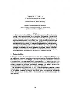
UNI-based 2
2 2 Exchange/Bypass Switch.
bitrarily short packets so as to improve time slot utilization [7], while being capable to withstand future line rate increases. II. EXPERIMENTS AND RESULTS For the operation of an optically addressable 2 2 exchangebypass switch three optical signals are needed, two data signals, and one control signal. Data signals enter the switch from the input ports 1 and 2. If there is no control signal the switch is in the BAR state and both data signals pass straight through to the output ports 1 and 2. If the control signal is present, the switch is in the CROSS state and the two data streams are interchanged at its output. The length of the bit sequence that is interchanged through the switch is determined by the length of the control signal and may be arbitrarily long or short depending on the length of the incoming packet. The 2 2 switch uses a UNI gate, which has been configured to provide two inputs and outputs for counterpropagating signals as shown in Fig. 1. Data signals 1 and 2 enter through the input ports 1 and 2, respectively, via the ports 3 and 4 of the two polarization beam splitters (PBSs). The two data signals enter the SOA after traveling through identical lengths of birefringent fiber that are at the end sections of the UNI and are spliced at 45 with the output fibers of the two PBSs. As a result, each data pulse is separated into two orthogonal polarization components that are relatively delayed by half a bit period or 50 ps. The control signal is launched through a 80:20 fiber splitter so that it cotravels with data signal 2 and so that it is synchronized to the preceding of the two orthogonal polarization components of each data pulse. If there is no control signal, then data signal 1 exits through port 4 of the PBS and finally through output port 1 of the switch, while data signal 2 exits through port 3 of the other PBS, and finally through the output port 2 of the switch. In the presence of a control pulse, the phase of the two synchronized polarization components is changed, so that when the components of each data signal recombine at the PBSs their
1041-1135/02$17.00 © 2002 IEEE
THEOPHILOPOULOS et al.: OPTICALLY ADDRESSABLE 2
Fig. 2.
2 EXCHANGE/BYPASS PACKET SWITCH
999
Signals generator for first experiment.
polarization states rotate by 90 . In this way, data signal 1 exits through port 6 of the PBS and finally appears in output port 2 of the switch, while data signal 2 exits through port 5 of the other PBS and finally appears in output port 1 of the switch. In our implementation, the nonlinear element in the UNI gate was a 1.5-mm bulk InGaAsP–InP ridge waveguide SOA with small signal gain of 30 dB at 1560 nm with 700-mA drive current. The performance of the switch was investigated in two experiments. In the first experiment, the performance of the switch was evaluated at data packet level including different packet lengths. In this instance, the switch was used as a data packet exchanger and the input data signals emulated sequences of packets. In the second experiment, the error performance of the switch was evaluated in static configuration with input data of SDH/STM 64 format. In the first experiment, the signals that powered the switch (Fig. 1) were generated from the configuration of Fig. 2. The two gain-switched DFB diode lasers, LD1 and LD2 provided the data and control signals, respectively. LD1 operates at 1549.2 nm and was gain switched at 1.25 GHz so as to produce 8.1-ps pulses after linear compression. The pulse train was then modulated in a LiNbO modulator driven from a pseudorandom bit maximal length bit sepattern generator to produce a 2 quence at 1.25 Gb/s. The bit rate was optically multiplied by PRBS. Data eight times to 10 Gb/s, but so as to retain the 2 signal 1 was formed from this PRBS after being modulated in a LiNbO modulator driven from a pulse generator to produce variable length and period data packets. Data signal 2 was the full 10-Gb/s PRBS and was also obtained from LD1. The control signal was generated from LD2 driven at 10 GHz so as to produce 8.4-ps pulses after linear compression. This pulse train was then modulated in a LiNbO modulator, which was driven with an electrical pulse of 400-ps rise time resulting in the slow rise time of the control packets shown in Fig. 3(e). This however, did not affect the performance of the switch. For easy visualization in the present demonstration, the control signal packet had duration of 3.2 ns and period of 6.4 ns, while the data packet of signal 1 had duration of 2.5 ns and period of 6.4 ns. In this way, the input data signals can be viewed as sequences of data packets with fixed length of 3.2 ns or 32 bits long, while the control signal as a packet of 32 consecutive 1s with 3.2-ns duration and a period of 6.4 ns. Fig. 3 shows the two output ports of the switch monitored simultaneously on a 30-GHz sampling oscilloscope by using two photodiodes with different sensitivities. Fig. 3(a) and (c) show the input data signals 1 and 2 into the switch. Fig. 3(b) and (d) show the corresponding output signals for the BAR and CROSS
Fig. 3. BAR and CROSS states: (a), (c) input. (b), (d) output data streams. (e) control signal. The time base is 500 ps/div.
Fig. 4. Signals generator of Setup 2.
states, respectively, and Fig. 3(e) shows the control sequence. In the BAR state, the data packets from signals 1 and 2 depicted by the thick-dashed and thin-dotted lines, respectively, cross the switch unchanged. When the optical control signal is present, the switch is in the CROSS state and the packets are interchanged in the output ports. The pulse energies for the data 1, data 2, and control pulses were 2, 2, and 8 fJ, respectively. The crosstalk of the switch in the BAR and CROSS states was 12 and 10 dB, respectively, in the worst case. Crosstalk at port 1 (2) is defined as the power ratio of the leaked signal from port 2 (1) to the transmitted signal at port 1 (2) for both states of operation and it was estimated by bit to bit calculation from patterns like those of Fig. 3. In the presence of the control signal, there was also a 1-dB drop in the switched signals due to additional SOA gain saturation, that may be mitigated using a gain transparent arrangement [14]. It is important to note that if this exchange-bypass unit is used in an optical packet switch matrix it relaxes the requirement for guardbands between the packets, since the switch changes state within the bit period. In avoiding guardbands, the improvement in throughput becomes more pronounced as the packet length decreases. The switch was also evaluated with variable length packets including 43-ns ATM cells and showed similar behavior. In the second experiment, the signals that powered the switch (Fig. 1) were generated from the configuration of Fig. 4. A SDH/STM 64 Network Analyzer by Acterna generated SDH
1000
IEEE PHOTONICS TECHNOLOGY LETTERS, VOL. 14, NO. 7, JULY 2002
switching matrixes. The switch requires low pulse energy to switch and provided that there is active polarization control it will operate error free. Its main advantages are that since a state change may be affected within a bit period of a 10-Gb/s stream, there is no need for packet guardbands even for very short packets, and since the switch is optically addressable, high-speed electrical packaging requirements for the switching elements are relaxed. Given that the UNI switch has been operated to 40 Gb/s with a counterpropagate configuration [11], it is expected that the speed of this exchange-bypass switch is scalable at least up to this rate. Fig. 5. Eye measurements with (a), (b) STM 64 input frames. (c) BAR state. (d) CROSS state. The time base is 20 ps/div.
packets that contained a 2 maximal length bit sequence at 9.953 28 Gb/s. This time the clock output from the network analyzer was used to gain switch directly the diodes LD1 and LD2 at 9.953 28 GHz and generate 10-ps pulses trains after linear compression. Using the data output of the Network Analyzer, a LiNbO modulator was driven at 9.953 28 Gb/s and modulated the pulse train generated from LD1 providing a STM 64 data stream. This data stream was divided into two parts to provide the two data input streams and these were decorrelated in the switch by using different optical delays between them. LD2 provided the control stream and could be turned on or off to assess the switch states. Fig. 5 shows the eye measurements for the input and output signals from the switch. Fig. 5(a) and (b) show the eye diagrams for the two input data streams, which are identical. Fig. 5(c) shows the two streams for the BAR state in the absence of the control signal and Fig. 5(d) is the equivalent diagram for the CROSS state. The degradation of the eye diagrams at the output of the switch is due to cross talk and incomplete polarization extinction in the switch. The error rate was statistically calculated from the network analyzer by checking appropriate control bits for both data sigat each SDH packet and was less than 10 nals in both switch states. The switch is polarization sensitive due to the polarization gain dependence of the SOA, as well as the PM fiber arrangement in the UNI, so that the error rate would gradually increase as the polarization states of the interacting signals drifted. However, simple adjustment of the polarization controllers was sufficient to revert to the initial error free operation. This means that the switch may be operated error free with a closed loop electrical polarization controller. III. CONCLUSION We have demonstrated a 10-Gb/s optically addressable, 2 2 exchange bypass switch that may be used in optical packet
ACKNOWLEDGMENT The authors would like to thank G. Guekos of ETHZ, R. Dall’Ara and S. Hansmann of Opto Speed, S.A. for the SOA, and W. Miller of Acterna for lending the SDH/STM 64 Network Analyzer. REFERENCES [1] M. J. O’Mahony et al., “The application of optical packet switching in future communication networks,” IEEE Commun. Mag., vol. 19, pp. 128–135, 2001. [2] D. Benjamin et al., “Optical services over the intelligent optical network,” IEEE Commun. Mag., vol. 39, pp. 73–78, 2001. [3] G. Hjalmtysson et al., “Smart routers-simple optics: An architecture fot the optical internet,” J. Lightwave Technol., vol. 18, pp. 1880–1891, Dec. 2000. [4] M. Bachmann et al., “Polarization-Insensitive low-voltage optical waveguide switch using InGaAs/InP four-port Mach-Zehnder interferonmeter,” in Proc. Optical Fiber Communications (OFC), 1993, pp. 32–33. [5] D. Chiaroni et al., “Physical and logical validation of a network based on all-optical packet switching systems,” J. Lightwave Technol., vol. 16, pp. 2255–2264, Dec. 1998. [6] C. Guillemot et al., “Transparent optical packet switching: The european acts KEOPS project approach,” J. Lightwave Technol., vol. 16, pp. 2117–2134, Dec. 1998. [7] G. Soulage et al., “4 4 space-switch based on clamped-gain semiconductor optical amplifiers in 16 10 Gbits/s WDM experiment,” in Proc. Eur. Conf. Optical Communications (ECOC), 1996, Paper ThD.2.1. [8] N. Le Sauze et al., “Modular optical packet switching node for future multi-QoS metro networks,” in Proc. Eur. Conf. Optical Communications (ECOC) 2000, vol. 2, pp. 21–22. [9] D. Chiaroni et al., “First demonstration of an asynchronous optical packet switching matrix prototype for MultiTerabit class routers/switches,” in Proc. Eur. Conf. Optical Communications (ECOC) 2001, vol. 6, pp. 60–61. [10] K. E. Stubkjaer, “Semiconductor optical amplifier-based all-optical gates for high-speed optical processing,” IEEE J. Select. Topics Quantum Electron., vol. 6, pp. 1428–1435, Nov.–Dec. 2000. [11] N. S. Patel et al., “40-Gbit/s cascadable all-optical logic with an ultrafast nonlinear interferometer,” in Opt. Lett, vol. 21, 1996, pp. 1466–1468. [12] K. Tajima et al., “Ultrafast polarization—Discriminating Mach-Zehnder all—Optical switch,” Appl. Phys. Lett, vol. 67, pp. 3709–3711, 1995. [13] K. L. Hall et al., “100-Gbit/s bitwise logic,” Opt. Lett, vol. 23, pp. 1271–1273, 1998. [14] S. Diez et al., “Gain-Transparent SOA-switch for high-bitrate OTDM add/drop multiplexing,” IEEE Photon. Technol. Lett., vol. 11, pp. 60–62, Jan. 1999.
2
2