23rd Annual Review of Progress in Applied Computational Electromagnetics
March 19-23, 2007 - Verona, Italy ©2007 ACES
Optimizing Optical Negative Index Materials: Feedback from Fabrication Alexander V. Kildishev*, Uday K. Chettiar, Hsiao-Kuan Yuan, Wenshan Cai, and Vladimir M. Shalaev Birck Nanotechnology Center, Department of Electrical and Computer Engineering Purdue University, West Lafayette, IN 47907, USA
[email protected] Abstract: This work is concerned with challenges in optimizing optical metamaterials with a negative effective permeability and a negative effective permittivity (double-negative metamaterials, DNM). We demonstrate the huge importance of linking the fabrication parameters and the results of optical and structural characterization of fabricated prototypes with a given optimal design environment. Specifically, the role of material deposition rate in the performance of optical plasmonic metamaterials is studied. Initially, simpler prototype samples with a negative effective permeability in the visible range have been optimized and subsequently fabricated using different material deposition rates in an electron beam evaporation system. A lower deposition rate resulted in a better quality metallic surface and consequently a lower loss. To simulate the effect of metallic surface roughness, an adjustment of the complex permittivity for silver is performed in each sample by fitting the transmission and reflection spectra. The adjustment is introduced by a wavelength-dependent ‘lossfactor’ for the imaginary part of bulk metal permittivity. An averaged constant loss-factor is chosen for the best available fabrication technique and is used in the optimal design of DNM prototypes. A fabricated DNM sample is in good agreement with the results of the pre-fabrication optimization. The sample is double-negative for wavelengths between 805 and 815 nm with a real part of refractive index of about -1.0 at 813 nm, while the ratio -Re(n)/Im(n) reaches a maximum value of close to 1.3 at that wavelength. Keywords: double-negative metamaterial, negative index metamaterial, negative refraction.
1. Introduction Optical negative index metamaterials (NIMs) are artificially engineered metal-dielectric composites that exhibit n ′ < 0 within a certain range of wavelengths1. The magnetic resonant behavior should be observed in NIMs at this range, since this is always required to make the real part of the effective refractive index negative, either through the strong (sufficient) condition µ ′ < 0 and ε ′ < 0 , or through a more general necessary condition ε ′µ ′′ + µ ′ε ′′ < 0 . The general condition strictly implies that there is no negative refraction effect in a passive metamaterial with µ = 1 + 0ι . We note that the ratio − n ′ n ′′ is often taken as a figure of merit (FOM) for optimizing NIMs performance, since low-loss NIMs are desired. The FOM can be rewritten as − ( µ ε ′ + ε µ ′ ) ( µ ε ′′ + ε µ ′′ ) , indicating that a double-negative metamaterial (DNM) with µ ′ < 0 and ε ′ < 0 is better than a NIM with the same n ′ < 0 , but with µ ′ > 0 . In recent years, the area of optimal (inverse) designs of optical metamaterials has rapidly grown in importance. In the design of double-negative metamaterials (DNMs), the optimization approaches are mainly focused on the best layouts for sub-wavelength-scale lamellar metal-dielectric structures. The key part of designing DNMs is obtaining the maximum resonant negative magnetic response (negative effective permeability) from the periodic nanoscale elements while simultaneously providing the required negative permittivity.
1
A general notation a = a ′ + ιa ′′ for any complex number a is used in this paper.
943
23rd Annual Review of Progress in Applied Computational Electromagnetics
March 19-23, 2007 - Verona, Italy ©2007 ACES
Interest in the inverse design of optical DNMs has also increased greatly due to recent deterministic fabrication techniques that can create required nanoscale plasmonic elements reproducibly. This interest in the inverse design of optical metamaterials has been strongly influenced by nature-inspired approaches to stochastic optimization. Counter to the genetic algorithm (GA) [1] - [3], which is an established optimization method built on the principles of survival-of-the-fittest in simulated genetic evolution, the swarm intelligence (or the particle swarm optimization, PSO) is a relatively new stochastic optimization technique [4]. In contrast to GA, where the driving force is competition, PSO is driven by cooperation [5], [6]. Details of GA and PSO optimization of NIMs performed in collaboration with Prof. D. Werner’s group (Penn State University, USA) will be discussed elsewhere. This work does not cover a new optimization technique or an application of traditional optimization methods to designing new DNMs. Instead we emphasize the huge importance of feedback data coming from actual fabrication processes. To introduce design-specific and fabrication-specific adjustments to our optimization techniques, we seek to capture the critical manufacturing parameters by monitoring changes in optical properties of actual prototypes produced under differing conditions. Thus, we emphasize the significance of linking the fabrication parameters and the results of optical and structural characterization of DNM prototypes with a given optimal design environment. Along with the challenges of fabricating nanoscale structures using electron beam lithography (EBL), losses in metallic elements also limit the practical applications of DNMs in optics. Although silver has been already selected for the metallic elements in our DNM prototypes because of its low loss, the surface roughness of silver-dielectric interfaces, unfortunately unavoidable in EBL, adds even more difficulties. Similar to losses in bulk silver, the roughness-induced loss enhancement is also wavelength dependent. In contrast to the bulk metal loss, however, this fabrication- and design-specific dependency is normally unknown a priori. Thus, surface roughness substantially complicates optimization by contributing an additional loss that is difficult to predict. There are conflicting views on how to minimize additional diffusive and absorptive losses generated by surface roughness. Some researchers believe that increasing the deposition rate of silver could improve the surface quality, resulting in lower RMS roughness and in lower loss [7]. The rationale behind this thinking is that the high deposition rate counteracts the tendency of the highly mobile silver particles to form islands. With a slower deposition rate the silver would start forming islands resulting in a rough silver film, which may even become semi-continuous if the layer is too thin. But, it could also be argued that a slower deposition rate would allow the silver layer to stabilize itself by minimizing the free energy, thus reducing the number of defects and resulting in a lower loss. It is of prime importance to understand the effect of fabrication on the metal used in optimized plasmonic structures since it could drastically affect the design output and the final performance. Hence, in this paper we specifically address the effect of deposition rate on the optical properties of optimized DNM structures. First, the effect of the deposition rate on the magnetic resonances is analyzed for a simpler system consisting of a periodic array of paired nanostrips. The system is very similar to a grating. In this structure only the effective permeability is negative ( µ ′ < 0 , ε ′ > 0 ) . For this material, ε ′′ for bulk silver is multiplied by a wavelength-dependent “loss-factor” to match the simulated absorption with the experimental data. Then, an average loss-factor (for the best deposition rate) is employed in the design of a bi-periodic DNM prototype which is similar to a crossed grating in appearance. Finally, the experimental transmission and reflection spectra of the fabricated prototype are compared to the simulated data, successfully validating our method of introducing additional loss to the plasmonic elements for the optimal design of DNG in optics. 2. Effect of deposition rates on resonances in paired nanostrips Metal-dielectric composites with a negative effective permeability are essential for further development of low-loss optical DNMs. Recent simulations and experiments [8], [9] have demonstrated that pairs of
944
23rd Annual Review of Progress in Applied Computational Electromagnetics
March 19-23, 2007 - Verona, Italy ©2007 ACES
thin silver strips separated by a dielectric spacer could offer an easy way of achieving negative effective permeability by coupling near-field modes. In addition, the layer of the pairs of silver strips with sub-wavelength periodicity is much simpler to model and fabricate than a layer of bi-periodic DNM. Provided that the magnetic field of the normally-incident and linearlypolarized light is directed parallel to the strip edges, the layer of paired nanostrips is known to have two distinct resonant responses. Relative to the midplane of the layer, the resonances exhibit distinct symmetries of their dominant propagating E-field modes. Thus, in contrast to the dominant symmetric mode of the ‘electric’ resonance at a shorter wavelength giving a negative effective permittivity ( ε ′ < 0 , µ ′ > 0 ) to the layer, the dominant asymmetric mode of the ‘magnetic’ resonance at a longer wavelength results in a negative effective permeability ( µ ′ < 0 , ε ′ > 0 ). It has also been shown that the dominant propagating mode of the scattered field in a periodic array of coupled silver strips is always accompanied by a weaker response with the opposite symmetry and reversed dispersion behavior. For example, the magnetic resonance is always accompanied by an electric anti-resonance. This phenomenon does not occur for the case of an isolated strip pair of the same structural dimensions and materials.
(a)
H E
(b) H E
Figure 1: (a) Field emission scanning electron microscope (FE SEM) image of Sample A (deposited at 0.5 Å/s). (b) FE SEM image of Sample С (deposited at 10.0 Å/s).
We studied the effect of deposition rates on these resonances using actual prototype samples of optimized structures. The samples were fabricated using electron beam lithography techniques. First, the geometry of the periodic, thin silver strips was defined by using an electron beam writer on a glass substrate initially coated with a 15-nm film of indium-tin-oxide (ITO). Then, electron beam evaporation was applied to produce a stack of lamellar films. Finally, a lift-off process was performed to obtain the desired silver strips. The projected serial structure of the films from the ITO-coated glass was: Sample A and C, 10 nm alumina, 35 nm silver, 40 nm alumina, 35 nm silver, 10 nm alumina; Sample B, 10 nm alumina, 30 nm silver, 40 nm alumina, 30 nm silver, 10 nm alumina. The deposition rates were 0.5 Å/s, 2.5 Å/s and 10.0 Å/s for Sample A, B and C respectively. Field emission scanning electron microscope (FE SEM) images of Sample A and Sample С are shown in Figure 1ab. The periodicity of all the samples was 300 nm. Due to limitations in fabrication, the cross section of the nanostrip pair is trapezoidal instead of rectangular. This is a well known problem associated with fabrication methods that rely on positive photoresist, deposition and lift-off. This problem could be alleviated through the use of more sophisticated fabrication methods (dry etching or anisotropic etching). Unfortunately such methods have not yet been implemented for silver. The bottom widths of the nano-strip pairs averaged from representative FE SEM images were as follows, Sample A: 160 nm, Sample B: 174 nm, Sample C: 160 nm. The top widths were as follows, Sample A: 85 nm, Sample B: 94 nm, Sample C: 80 nm. To test the fabricated samples, we measured the transmission and reflection spectra using an ultrastable tungsten lamp (B&W TEK BPS100). The spectral range of the lamp covers the entire visible and near-infrared optical band. A Glan Taylor prism was placed at the output of the broadband lamp to select the light with desired linear polarization (as shown in Figure 1). The signal transmitted (or reflected) from the sample was introduced into a spectrograph (Acton SpectraPro 300i) and eventually collected by a liquid nitrogen cooled CCD-array detector. The transmission and reflection spectra were normalized to a bare substrate and a calibrated silver mirror, respectively. The initial optimal design of the prototypes was performed using a commercial finite element solver with the material properties of bulk silver taken from experimental data [10]. Since the losses in the silver elements of the metamaterial appeared to be invariably larger than that of bulk silver mainly due to surface roughness, we modeled the contribution from this loss enhancement through a wavelength-dependent adjustment factor ( α , loss-factor), such that the permittivity of silver was given by ε = ε ′ + iαε ′′ , where
945
23rd Annual Review of Progress in Applied Computational Electromagnetics
8
1 Sample A Sample B Sample C
14 T (simulation) R (simulation) T (experiment) R (experiment)
(a) 0.8
(b)
12 10
permeability (µ')
loss factor (α)
6
March 19-23, 2007 - Verona, Italy ©2007 ACES
0.6 4 0.4 2
Sample A Sample B Sample C
(с)
8 6 6 2 0
0.2
2 0 500
600
700 wavelength (nm)
800
900
0 400
500
600 700 wavelength (nm)
800
900
650
700
750 wavelength (nm)
800
850
Figure 2: (a) Spectrum of the loss factor (α) for the three Samples. (b) Transmission and Reflection spectrum for Sample A. Dashed line shows the simulated spectrum and continuous line shows the experimental spectrum. (c) The real part of the effective permeability for the three samples.
the real and imaginary parts of the permittivity of bulk silver ( ε ′ and [10]. Our further experimental studies showed that α is in general simulated absorbance was matched to the experimental absorbance length-dependent loss-factor α .
ε ′′ ) have also been taken from Ref.
a function of the wavelength. The by incorporating a suitable wave-
3. Modeling of the roughness-enhanced losses The loss-factor spectrum for the three samples is shown in Figure 2a. For example, the simulation results of Sample A with the adjusted loss-factor are compared to the spectral measurements in Figure 2b. We note that the simulations match the experiment very closely. The corresponding spectra of Samples B and C (not shown) also demonstrate excellent matching between the simulated and experimental data. For Sample A, two valleys in the transmission spectrum indicate the position of the electrical resonance (at a wavelength of 516 nm) and the magnetic resonance (at a wavelength of 727 nm). We note that for all samples the loss-factor is always higher at both resonances. Moreover, the loss-factor is higher at the magnetic resonance as compared to the electrical resonance. Additional evanescent modes at the resonances create stronger fields that are localized near the metal structures and therefore provide an enhanced field interaction with the rough features of nanoscale relief at the metal-dielectric interfaces. This gives a higher loss-factor near the resonance wavelengths. The asymmetric modes of the magnetic resonance appeared to be more sensitive to the surface irregularities. As a result, loss-factor is even higher at the magnetic resonance as compared to the electrical resonance. Figure 2a indicates that the maximum of the loss-factor falls with a decrease in the deposition rate. This leads us to conclude that a slower deposition rate results in better quality and consequently lower loss in the deposited silver. Figure 2c shows the real part of permeability for the three samples, indicating that a lower loss-factor results in a more negative permeability. The results are summarized in Table 1. 4. Double negative materials based on fishnet geometry It has been previously shown that a subwavelength bi-periodic grating (‘fishnet’) consisting of two metal layers separated by a dielectric layer can provide a negative index material [11] - [12]. The incident light is polarized along one of the gratings (see Figure 3a). The grating that is aligned with the incident magnetic field provides negative permeability Table 1: Summary of the results for the three samples through a magnetic resonance as seen in the previous section. In an optimized structure the Sample Deposition rate of silver (Å/s) Min(µ) Max(α) magnetic resonance can be sufficiently strong A 0.5 -1.7+4i 4.2 to yield a negative permeability. The other grating is aligned with the incident electric B 2.5 -0.94+3.4i 6.0 field and shows no resonances or diffraction (since the period is subwavelength). Similar to C 10 -0.85+3i 7.7 the approach shown in [9], this grating be-
946
23rd Annual Review of Progress in Applied Computational Electromagnetics
March 19-23, 2007 - Verona, Italy ©2007 ACES
1
(a)
(b)
T (simulation) R (simulation) T (experiment) R (experiment)
0.8
0.6
H
0.4
0.2
0
2
700
E
750
800 850 wavelength (nm)
900
(c)
FOM n’
950
(d) 2
1 0
0
2
1
2 700
750
800 850 wavelength (nm)
900
4 700
950
ε' µ' 750
800 850 wavelength (nm)
900
950
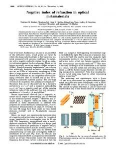
Figure 3: (a) SEM image of DNM sample. (b) Transmission and reflectance spectrum for DNM sample. The dashed line shows the simulated spectrum and the continuous line shows the experimental spectrum. (c) Effective refractive index and FOM of the DNM sample. (d) Effective permeability and permittivity of the DNM sample.
haves like a dilute metal providing a negative permittivity. In a properly designed structure this could lead to simultaneous negative permeability and permittivity, resulting in a DNM. We have already demonstrated that the effective properties of metallic elements in a nanostructured metamaterial depend on the method of fabrication. This presents a difficulty in optimizing such nanostructures using only the properties of bulk metal. Hence, constant feedback from fabrication and measurements is required to find the optimum design. As a simplified approach, an averaged value of loss-factor α can be used for optimization of the prototypes fabricated with a selected deposition rate. For example, a constant value ( α = 3 ) was taken to optimize a DNM prototype. 5. Results and discussions A DNM sample with a period of 300 nm (in both directions) was fabricated and characterized using methods described in the previous sections. The polarization of incident light used for characterizing the sample and its FE SEM image are shown in Figure 3a. The deposition of silver was performed at a rate of 0.5 Å/s. Figure 3b shows the experimental and simulated spectra of the sample. The simulations are in excellent agreement with optical measurements. Figure 3c shows the effective refractive index of the sample. The real part of the refractive index is negative in the 60-nm range from 790 nm to 850 nm. Figure 3d show the effective permeability and permittivity. The permittivity demonstrates ‘metallic behavior’ with the negative real part becoming increasingly negative with increasing wavelength, while the permeability shows a strong resonant behavior; as a result the real part of permeability is negative from 805 nm to 815 nm. The sample is double negative for wavelengths between 805 and 815 nm. Figure 3c shows the FOM of the sample given by the ratio − n ′ n ′′ . The FOM reaches a maximum value of around 1.3 at 813 nm, where n ′ ≈ −1.0 .
947
23rd Annual Review of Progress in Applied Computational Electromagnetics
March 19-23, 2007 - Verona, Italy ©2007 ACES
Acknowledgments We would like to acknowledge valuable help of Dr. Drachev from the Birk Nanotechnology Center, Purdue University, USA. We highly appreciate his kind assistance with all the critical aspects of this work. We also would like to cite productive collaboration with Prof. Werner’s group at Penn State University, USA. This work was supported in part by ARO grant W911NF-04-1-0350, NSF-PREM grant #DMR0611430 and by ARO-MURI award 50342-PH-MUR. References [1] [2] [3] [4] [5] [6] [7] [8] [9] [10] [11] [12] [13]
R. L. Haupt and S. E. Haupt, Practical Genetic Algorithms, Hoboken, New Jersey: WileyInterscience, 2004. Y. Rahmat-Samii and E. Michelssen, eds., Electromagnetic Optimization by Genetic Algorithms, Hoboken, New Jersey: Wiley-Interscience, 1999. S. Chakravarty, R. Mittra, and N. R. Williams, “Application of a micro-genetic algorithm (MGA) to the design of broad-band microwave absorbers using multiple frequency selective surface screens buried in dielectrics,” IEEE Trans. Antennas Propag., vol. 50, no. 3, pp. 284–296, Mar. 2002. J. Kennedy and R. C. Eberhart, Swarm Intelligence, Academic Press, 2001. D. W. Boeringer and D. H. Werner, “Particle swarm optimization versus genetic algorithms for phased array synthesis,” IEEE Trans. Antennas Propag., vol. 52, no. 3, pp. 771–779, Mar. 2004. D. W. Boeringer and D. H. Werner, “Efficiency-constrained particle swarm optimization of a modified Bernstein polynomial for conformal array excitation amplitude synthesis,” IEEE Trans. Antennas Propag., vol. 53, no. 8, pp. 2662–2673, Aug. 2005. N. Fang, H. Lee, C. Sun, and X. Zhang, “Sub-Diffraction-Limited Optical Imaging with a Silver Superlens,” Science, vol. 308, no. 5721, pp. 534–537, Apr. 2005. H.-K. Yuan, U. K. Chettiar, Wenshan Cai, A. V. Kildishev, A. Boltasseva, V. P. Drachev, and V. M. Shalaev, “A negative permeability material at red light,” Opt. Express, to be published. Available: http://arxiv.org/abs/physics/0610118, (2006). U. K. Chettiar, A. V. Kildishev, T. A. Klar, and V. M. Shalaev, “Negative index metamaterial combining magnetic resonators with metal films,” Opt. Express, vol. 14, no. 17, pp. 7872–7877, Aug. 2006. P. B. Johnson and R. W. Christy, “Optical constants of the noble metals,” Phys. Rev. B, vol. 6, no. 12, pp. 4370–4379, Dec. 1972. S. Zhang, W. Fan, N. C. Panoiu, K. J. Malloy, R. M. Osgood, and S. R. J. Brueck, “Experimental demonstration of near-infrared negative-index metamaterial,” Phys. Rev. Lett., vol. 95, pp. 137404 Sept. 2005. G. Dolling, C. Enkrich, M. Wegener, C. M. Soukoulis, and S. Linden, “Simultaneous negative phase and group velocity of light in a metamaterial,” Science, vol. 312, no. 5775, pp. 892–894, May 2006. G. Dolling, M. Wegener, C. M. Soukoulis, and S. Linden, “Negative-index metamaterial at 780 nm wavelength,” Opt. Lett., vol. 32, no. 1, pp. 53–55, Jan. 2006.
948